 Datasheet下载
- 型号: ATSHA204-MAH-DA-T
- 制造商: Atmel
- 库位|库存: xxxx|xxxx
- 要求:
| 数量阶梯 | 香港交货 | 国内含税 |
| +xxxx | $xxxx | ¥xxxx |
查看当月历史价格
查看今年历史价格
ATSHA204-MAH-DA-T产品简介:
ICGOO电子元器件商城为您提供ATSHA204-MAH-DA-T由Atmel设计生产,在icgoo商城现货销售,并且可以通过原厂、代理商等渠道进行代购。 ATSHA204-MAH-DA-T价格参考。AtmelATSHA204-MAH-DA-T封装/规格:专用 IC, Authentication Chip IC Networking and Communications 8-UDFN (2x3)。您可以下载ATSHA204-MAH-DA-T参考资料、Datasheet数据手册功能说明书,资料中有ATSHA204-MAH-DA-T 详细功能的应用电路图电压和使用方法及教程。
Microchip Technology 的 ATSHA204-MAH-DA-T 是一款专用 IC,属于安全认证类芯片,主要用于提供安全密钥存储和身份认证功能。该芯片支持 SHA-256 加密算法,具备硬件级安全防护能力,防止密钥泄露和非法访问。

其典型应用场景包括:

1. 物联网设备认证:用于确保设备的身份真实,防止假冒设备接入系统。
2. 访问控制:在门禁系统或权限管理系统中,作为安全令牌实现高安全级别的身份验证。
3. 消费电子产品防伪:嵌入在高端设备中,验证产品真伪,防止假冒产品进入市场。
4. 工业控制系统:用于保护关键设备的访问权限,确保只有经过认证的组件可以通信或操作。
5. 软件授权与许可管理:作为硬件密钥,用于保护软件许可信息,防止未经授权的使用。

该芯片因其高安全性、低功耗和小封装,广泛适用于对安全性要求较高的嵌入式系统和智能设备中。
| 参数 | 数值 |
| 产品目录 | 集成电路 (IC)半导体 |
| 描述 | IC CRYPTO 4.5KB I2C 8UDFN特定功能逻辑 CryptAuthEE SHA256 I2C |
| 产品分类 | |
| 品牌 | Atmel |
| 产品手册 | |
| 产品图片 |
|
| rohs | 符合RoHS无铅 / 符合限制有害物质指令(RoHS)规范要求 |
| 产品系列 | 逻辑集成电路,特定功能逻辑,Atmel ATSHA204-MAH-DA-TCryptoAuthentication™ |
| 数据手册 | |
| 产品型号 | ATSHA204-MAH-DA-T |
| PCN封装 | |
| PCN设计/规格 | |
| PCN过时产品 | |
| 产品种类 | 特定功能逻辑 |
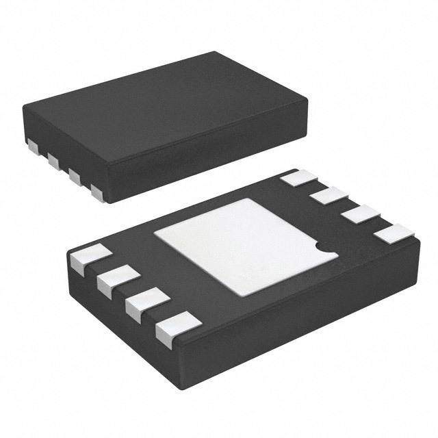
| 供应商器件封装 | 8-UDFN(2x3) |
| 其它名称 | ATSHA204-MAH-DA-T SL901CT |
| 包装 | Digi-Reel® |
| 商标 | Atmel |
| 安装类型 | 表面贴装 |
| 安装风格 | SMD/SMT |
| 封装 | Reel |
| 封装/外壳 | 8-UFDFN 裸露焊盘 |
| 封装/箱体 | UDFN-8 |
| 工作电源电压 | 2 V to 5.5 V |
| 工厂包装数量 | 5000 |
| 应用 | 网络和通信 |
| 标准包装 | 1 |
| 类型 | 验证芯片 |
| 视频文件 | http://www.digikey.cn/classic/video.aspx?PlayerID=1364138032001&width=640&height=505&videoID=2226387988001http://www.digikey.cn/classic/video.aspx?PlayerID=1364138032001&width=640&height=505&videoID=2226387984001http://www.digikey.cn/classic/video.aspx?PlayerID=1364138032001&width=640&height=505&videoID=2226387980001 |
| 配用 | /product-detail/zh/AT88CK9000-8MA/AT88CK9000-8MA-ND/3481155 |


- 商务部:美国ITC正式对集成电路等产品启动337调查
- 曝三星4nm工艺存在良率问题 高通将骁龙8 Gen1或转产台积电
- 太阳诱电将投资9.5亿元在常州建新厂生产MLCC 预计2023年完工
- 英特尔发布欧洲新工厂建设计划 深化IDM 2.0 战略
- 台积电先进制程称霸业界 有大客户加持明年业绩稳了
- 达到5530亿美元!SIA预计今年全球半导体销售额将创下新高
- 英特尔拟将自动驾驶子公司Mobileye上市 估值或超500亿美元
- 三星加码芯片和SET,合并消费电子和移动部门,撤换高东真等 CEO
- 三星电子宣布重大人事变动 还合并消费电子和移动部门
- 海关总署:前11个月进口集成电路产品价值2.52万亿元 增长14.8%


PDF Datasheet 数据手册内容提取
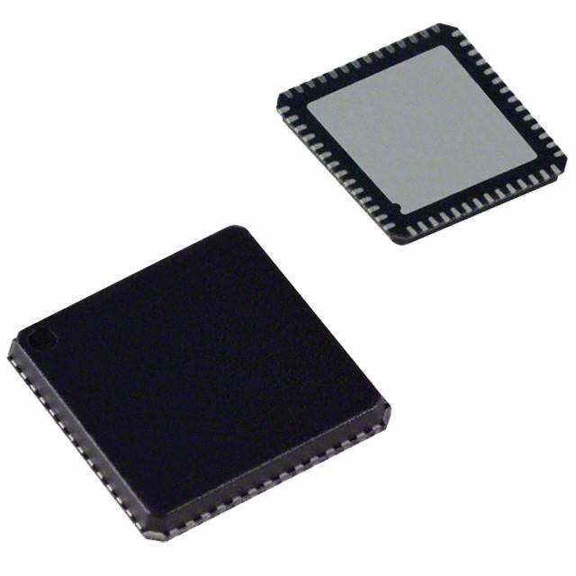
ATSHA204 Atmel CryptoAuthentication NOT RECOMMENDED DATASHEET FOR NEW DESIGNS Replaced by Features ATSHA204A Secure authentication and validation device Integrated capability for both Host and Client operations Superior SHA-256 Hash algorithm with Message Authentication Code (MAC) and Hash-Based Message Authentication Code (HMAC) options Best-in-class, 256-bit key length; storage for up to 16 keys Guaranteed unique 72-bit serial number Internal, high-quality Random Number Generator (RNG) 4.5Kb EEPROM for keys and data 512 OTP (One Time Programmable) bits for fixed information Multiple I/O options High-Speed, Single-Wire Interface 1MHz I2C interface 2.0V to 5.5V supply voltage range 1.8V to 5.5V communications <150nA sleep current Extended, multi-level hardware security 8-lead SOIC, 8-lead TSSOP, 3-lead SOT23, 8-pad UDFN, and 3-lead Contact packages Applications Anti-clone protection for accessories, daughter cards, and consumables Secure boot validation, software anti-piracy Network and computer access control Key exchange for encrypted downloads Authenticated/encrypted communications for control networks Atmel-8740H-CryptoAuth-ATSHA204-Datasheet_072014
Table 1. Pin Configurations Pin Name Function NC No Connect GND Ground SDA Serial Data SCL Serial Clock Input V Power Supply CC Figure 1. Pinouts 8-lead SOIC 8-lead TSSOP NC 1 8 V NC 1 8 V CC CC NC 2 7 NC NC 2 7 NC NC 3 6 SCL NC 3 6 SCL GND 4 5 SDA GND 4 5 SDA Top View Top View 3-lead SOT23 8-pad UDFN V 8 1 NC 2 V CC CC NC 7 2 NC GND 3 SCL 6 3 NC SDA 5 4 GND 1 SDA Bottom View Top View 3-lead Contact 1 SDA 2 GND 3 V CC Bottom View 2 ATSHA204 [DATASHEET] Atmel-8740H-CryptoAuth-ATSHA204-Datasheet_072014
Table of Contents 1. Introduction. . . . . . . . . . . . . . . . . . . . . . . . . . . . . . . . . . . . . . . . . . . . . 6 1.1 Applications . . . . . . . . . . . . . . . . . . . . . . . . . . . . . . . . . . . . . . . . . . . . . . . . . . . 6 1.2 Device Features . . . . . . . . . . . . . . . . . . . . . . . . . . . . . . . . . . . . . . . . . . . . . . . . 6 1.3 Cryptographic Operation . . . . . . . . . . . . . . . . . . . . . . . . . . . . . . . . . . . . . . . . . 7 2. Device Organization . . . . . . . . . . . . . . . . . . . . . . . . . . . . . . . . . . . . . . 8 2.1 EEPROM Organization . . . . . . . . . . . . . . . . . . . . . . . . . . . . . . . . . . . . . . . . . . 8 2.1.1 Data Zone . . . . . . . . . . . . . . . . . . . . . . . . . . . . . . . . . . . . . . . . . . . . . 9 2.1.2 Configuration Zone . . . . . . . . . . . . . . . . . . . . . . . . . . . . . . . . . . . . . 10 2.1.3 One Time Programmable (OTP) Zone . . . . . . . . . . . . . . . . . . . . . . 14 2.1.4 Device Locking . . . . . . . . . . . . . . . . . . . . . . . . . . . . . . . . . . . . . . . . 15 2.2 Static RAM (SRAM) . . . . . . . . . . . . . . . . . . . . . . . . . . . . . . . . . . . . . . . . . . . . 17 2.2.1 TempKey . . . . . . . . . . . . . . . . . . . . . . . . . . . . . . . . . . . . . . . . . . . . . 17 3. Security Features . . . . . . . . . . . . . . . . . . . . . . . . . . . . . . . . . . . . . . . 18 3.1 Physical Security . . . . . . . . . . . . . . . . . . . . . . . . . . . . . . . . . . . . . . . . . . . . . . 18 3.2 Random Number Generator (RNG) . . . . . . . . . . . . . . . . . . . . . . . . . . . . . . . . 18 4. General I/O Information . . . . . . . . . . . . . . . . . . . . . . . . . . . . . . . . . . 19 4.1 Byte and Bit Ordering . . . . . . . . . . . . . . . . . . . . . . . . . . . . . . . . . . . . . . . . . . . 19 4.1.1 Output Example . . . . . . . . . . . . . . . . . . . . . . . . . . . . . . . . . . . . . . . . 19 4.1.2 MAC Message Example . . . . . . . . . . . . . . . . . . . . . . . . . . . . . . . . . 19 5. Single-Wire Interface . . . . . . . . . . . . . . . . . . . . . . . . . . . . . . . . . . . . 20 5.1 I/O Tokens . . . . . . . . . . . . . . . . . . . . . . . . . . . . . . . . . . . . . . . . . . . . . . . . . . . 21 5.2 I/O Flags . . . . . . . . . . . . . . . . . . . . . . . . . . . . . . . . . . . . . . . . . . . . . . . . . . . . . 21 5.2.1 Transmit Flag . . . . . . . . . . . . . . . . . . . . . . . . . . . . . . . . . . . . . . . . . . 21 5.3 Synchronization . . . . . . . . . . . . . . . . . . . . . . . . . . . . . . . . . . . . . . . . . . . . . . . 22 5.3.1 I/O Timeout . . . . . . . . . . . . . . . . . . . . . . . . . . . . . . . . . . . . . . . . . . . 22 5.3.2 Synchronization Procedures . . . . . . . . . . . . . . . . . . . . . . . . . . . . . . 22 5.4 Sharing the Interface . . . . . . . . . . . . . . . . . . . . . . . . . . . . . . . . . . . . . . . . . . . 22 5.5 Transaction Example . . . . . . . . . . . . . . . . . . . . . . . . . . . . . . . . . . . . . . . . . . . 23 5.6 Wiring Configuration for Single-Wire Interface . . . . . . . . . . . . . . . . . . . . . . . . 24 6. I2C Interface . . . . . . . . . . . . . . . . . . . . . . . . . . . . . . . . . . . . . . . . . . . 25 6.1 I/O Conditions . . . . . . . . . . . . . . . . . . . . . . . . . . . . . . . . . . . . . . . . . . . . . . . . 25 6.1.1 Device is Asleep . . . . . . . . . . . . . . . . . . . . . . . . . . . . . . . . . . . . . . . 25 6.1.2 Device is Awake . . . . . . . . . . . . . . . . . . . . . . . . . . . . . . . . . . . . . . . 25 6.2 I2C Transmission to the ATSHA204 Device . . . . . . . . . . . . . . . . . . . . . . . . . . 27 6.2.1 Word Address Values . . . . . . . . . . . . . . . . . . . . . . . . . . . . . . . . . . . 28 6.2.2 Command Completion Polling . . . . . . . . . . . . . . . . . . . . . . . . . . . . . 28 6.3 I2C Transmission from the ATSHA204 Device . . . . . . . . . . . . . . . . . . . . . . . . 28 6.4 Address Counter . . . . . . . . . . . . . . . . . . . . . . . . . . . . . . . . . . . . . . . . . . . . . . 29 6.5 I2C Synchronization . . . . . . . . . . . . . . . . . . . . . . . . . . . . . . . . . . . . . . . . . . . . 29 6.6 Transaction Example . . . . . . . . . . . . . . . . . . . . . . . . . . . . . . . . . . . . . . . . . . . 30 ATSHA204 [DATASHEET] 3 Atmel-8740H-CryptoAuth-ATSHA204-Datasheet_072014
7. Electrical Characteristics. . . . . . . . . . . . . . . . . . . . . . . . . . . . . . . . . . 31 7.1 Absolute Maximum Ratings . . . . . . . . . . . . . . . . . . . . . . . . . . . . . . . . . . . . . . 31 7.2 Reliability . . . . . . . . . . . . . . . . . . . . . . . . . . . . . . . . . . . . . . . . . . . . . . . . . . . . 31 7.3 AC Parameters — All I/O Interfaces . . . . . . . . . . . . . . . . . . . . . . . . . . . . . . . 31 7.3.1 AC Parameters — Single-Wire Interface . . . . . . . . . . . . . . . . . . . . . 32 7.3.2 AC Parameters — I2C Interface . . . . . . . . . . . . . . . . . . . . . . . . . . . . 34 7.4 DC Parameters — All I/O Interfaces . . . . . . . . . . . . . . . . . . . . . . . . . . . . . . . 35 7.4.1 V and V Specifications . . . . . . . . . . . . . . . . . . . . . . . . . . . . . . . . 35 IH IL 8. Control Flags. . . . . . . . . . . . . . . . . . . . . . . . . . . . . . . . . . . . . . . . . . . 37 8.1 I/O Blocks . . . . . . . . . . . . . . . . . . . . . . . . . . . . . . . . . . . . . . . . . . . . . . . . . . . . 37 8.1.1 Status/Error Codes . . . . . . . . . . . . . . . . . . . . . . . . . . . . . . . . . . . . . 38 8.2 Sleep Sequence . . . . . . . . . . . . . . . . . . . . . . . . . . . . . . . . . . . . . . . . . . . . . . . 39 8.3 Idle Sequence . . . . . . . . . . . . . . . . . . . . . . . . . . . . . . . . . . . . . . . . . . . . . . . . 39 8.4 Wake Sequence . . . . . . . . . . . . . . . . . . . . . . . . . . . . . . . . . . . . . . . . . . . . . . . 39 8.5 Watchdog Failsafe . . . . . . . . . . . . . . . . . . . . . . . . . . . . . . . . . . . . . . . . . . . . . 39 8.6 Command Sequence . . . . . . . . . . . . . . . . . . . . . . . . . . . . . . . . . . . . . . . . . . . 40 8.6.1 Command Packets . . . . . . . . . . . . . . . . . . . . . . . . . . . . . . . . . . . . . 40 8.6.2 Command Opcodes, Short Descriptions, and Execution Times . . . 41 8.6.3 Zone Encoding . . . . . . . . . . . . . . . . . . . . . . . . . . . . . . . . . . . . . . . . . 42 8.6.4 Address Encoding . . . . . . . . . . . . . . . . . . . . . . . . . . . . . . . . . . . . . . 43 8.6.5 CheckMac Command . . . . . . . . . . . . . . . . . . . . . . . . . . . . . . . . . . . 44 8.6.6 DeriveKey Command . . . . . . . . . . . . . . . . . . . . . . . . . . . . . . . . . . . . 46 8.6.7 DevRev Command . . . . . . . . . . . . . . . . . . . . . . . . . . . . . . . . . . . . . 48 8.6.8 GenDig Command . . . . . . . . . . . . . . . . . . . . . . . . . . . . . . . . . . . . . . 49 8.6.9 HMAC Command . . . . . . . . . . . . . . . . . . . . . . . . . . . . . . . . . . . . . . . 51 8.6.10 Lock Command . . . . . . . . . . . . . . . . . . . . . . . . . . . . . . . . . . . . . . . . 53 8.6.11 MAC Command . . . . . . . . . . . . . . . . . . . . . . . . . . . . . . . . . . . . . . . . 54 8.6.12 Nonce Command . . . . . . . . . . . . . . . . . . . . . . . . . . . . . . . . . . . . . . . 56 8.6.13 Pause Command . . . . . . . . . . . . . . . . . . . . . . . . . . . . . . . . . . . . . . . 58 8.6.14 Random Command . . . . . . . . . . . . . . . . . . . . . . . . . . . . . . . . . . . . . 59 8.6.15 Read Command . . . . . . . . . . . . . . . . . . . . . . . . . . . . . . . . . . . . . . . . 60 8.6.16 UpdateExtra Command . . . . . . . . . . . . . . . . . . . . . . . . . . . . . . . . . . 62 8.6.17 Write Command . . . . . . . . . . . . . . . . . . . . . . . . . . . . . . . . . . . . . . . . 63 9. Compatibility. . . . . . . . . . . . . . . . . . . . . . . . . . . . . . . . . . . . . . . . . . . 65 10.Mechanical . . . . . . . . . . . . . . . . . . . . . . . . . . . . . . . . . . . . . . . . . . . . 66 10.1 Pinout . . . . . . . . . . . . . . . . . . . . . . . . . . . . . . . . . . . . . . . . . . . . . . . . . . . . . . . 66 11.Package Drawings . . . . . . . . . . . . . . . . . . . . . . . . . . . . . . . . . . . . . . 67 11.1 8-lead SOIC . . . . . . . . . . . . . . . . . . . . . . . . . . . . . . . . . . . . . . . . . . . . . . . . . . 67 11.2 8-lead TSSOP . . . . . . . . . . . . . . . . . . . . . . . . . . . . . . . . . . . . . . . . . . . . . . . . 68 11.3 3-lead SOT23 . . . . . . . . . . . . . . . . . . . . . . . . . . . . . . . . . . . . . . . . . . . . . . . . . 69 11.4 8-pad UDFN . . . . . . . . . . . . . . . . . . . . . . . . . . . . . . . . . . . . . . . . . . . . . . . . . . 70 11.5 3-lead Contact . . . . . . . . . . . . . . . . . . . . . . . . . . . . . . . . . . . . . . . . . . . . . . . . 71 12.Ordering Information. . . . . . . . . . . . . . . . . . . . . . . . . . . . . . . . . . . . . 72 13.Errata . . . . . . . . . . . . . . . . . . . . . . . . . . . . . . . . . . . . . . . . . . . . . . . . 73 4 ATSHA204 [DATASHEET] Atmel-8740H-CryptoAuth-ATSHA204-Datasheet_072014
14.Reference and Application Notes. . . . . . . . . . . . . . . . . . . . . . . . . . . 74 14.1 SHA-256 . . . . . . . . . . . . . . . . . . . . . . . . . . . . . . . . . . . . . . . . . . . . . . . . . . . . . 74 14.2 HMAC/SHA-256 . . . . . . . . . . . . . . . . . . . . . . . . . . . . . . . . . . . . . . . . . . . . . . . 74 14.3 Key Values . . . . . . . . . . . . . . . . . . . . . . . . . . . . . . . . . . . . . . . . . . . . . . . . . . . 74 14.3.1 Diversified Keys . . . . . . . . . . . . . . . . . . . . . . . . . . . . . . . . . . . . . . . . 75 14.3.2 Rolled Keys . . . . . . . . . . . . . . . . . . . . . . . . . . . . . . . . . . . . . . . . . . . 75 14.3.3 Created Keys . . . . . . . . . . . . . . . . . . . . . . . . . . . . . . . . . . . . . . . . . . 75 14.3.4 Single-use Keys . . . . . . . . . . . . . . . . . . . . . . . . . . . . . . . . . . . . . . . . 75 14.3.5 Limited-use Key . . . . . . . . . . . . . . . . . . . . . . . . . . . . . . . . . . . . . . . . 76 14.3.6 Password Checking . . . . . . . . . . . . . . . . . . . . . . . . . . . . . . . . . . . . . 77 14.3.7 Transport Keys . . . . . . . . . . . . . . . . . . . . . . . . . . . . . . . . . . . . . . . . 78 15.Revision History . . . . . . . . . . . . . . . . . . . . . . . . . . . . . . . . . . . . . . . . 79 ATSHA204 [DATASHEET] 5 Atmel-8740H-CryptoAuth-ATSHA204-Datasheet_072014
1. Introduction The following sections introduce the features and functions of the Atmel® ATSHA204 authentication device. 1.1 Applications The ATSHA204 is a member of the Atmel CryptoAuthentication™ family of high-security hardware authentication devices. It has a flexible command set that allows use for many applications, including the following: Anti-counterfeiting Validate that a removable, replaceable, or consumable Client is authentic. Example Clients could be printer ink tanks, electronic daughter cards, or other spare parts. It can also be used to validate a software/firmware module or memory storage element. Protection for Firmware or Media Validate code stored in flash memory at boot to prevent unauthorized modifications (also known as secure boot), encrypt downloaded media files, and uniquely encrypt code images to be usable on a single system only. Session Key Exchange Securely and easily exchange stream encryption keys for use by an encryption/decryption engine in the system microprocessor to manage such things as a confidential communications channel or an encrypted download. Secure Data Storage Store secret keys for use by crypto accelerators in standard microprocessors. It can also be used to store small quantities of data necessary for configuration, calibration, ePurse value, consumption data, or other secrets. Programmable protection up through encrypted/authenticated reads and writes. User Password Checking Validate user entered passwords without letting the expected value become known, map simple passwords to complex ones, and securely exchange password values with remote system. 1.2 Device Features The ATSHA204 device includes an Electrically Erasable Programmable Read-Only Memory (EEPROM) array that can be used for storage of keys, miscellaneous read/write, read-only or secret data, consumption logging, and security configuration. Access to the various sections of memory can be restricted in a variety of ways and the configuration then locked to prevent changes. See Section 2.1, “EEPROM Organization” for more details. The ATSHA204 features a wide array of defensive mechanisms specifically designed to prevent physical attacks on the device itself or logical attacks on the data transmitted between the device and the system see Section 3., “Security Features” for more details. Hardware restrictions on the ways in which keys are used or generated provide further defense against certain styles of attack. Access to the device is through a standard I2C interface at speeds up to 1Mb/s. see Section 6., “I2C Interface” for more details. It is compatible with the I2C interface specifications. The device also supports a Single-Wire Interface that can reduce the number of GPIOs required on the system processor and/or reduce the number of pins on connectors. See Section 5., “Single-Wire Interface” for more details. Using the Single-Wire Interface, multiple ATSHA204 devices can share the same bus, which saves processor GPIO usage in systems with multiple Clients such as different color ink tanks or multiple spare parts. See Section 5.4, “Sharing the Interface” and Section 8.6.13, “Pause Command” for more details on the way in which this is implemented. Each ATSHA204 ships with a guaranteed unique 9-byte (72-bit) serial number. Using the cryptographic protocols supported by the device, a Host system or remote server can prove that the serial number is both authentic and is not a copy. Serial numbers are often stored in a standard Serial EEPROM, but these can be easily copied, and there is no way for the Host to know if the serial number is authentic or a clone. The entire serial number must be utilized to guarantee uniqueness. The ATSHA204 can generate high-quality random numbers and employ them for any purpose, including as part of the crypto protocols of this device. Because each 32-byte (256-bit) random number is not dependent on passed numbers generated on this or any other device, their inclusion in the protocol calculation ensures that replay attacks 6 ATSHA204 [DATASHEET] Atmel-8740H-CryptoAuth-ATSHA204-Datasheet_072014
(re-transmitting a previously successful transaction) always fail. See Section 3.2, “Random Number Generator (RNG)” and Section 8.6.14, “Random Command”. System integration is eased with a wide supply voltage range (2.0V through 5.5V) and an ultra-low sleep current of <150nA. Complete DC parameters are found in Section 7., “Electrical Characteristics”, which describes multiple package options, including a tiny SOT23 package with a footprint of only 2.5mm x 3mm. See Section 11., “Package Drawings” for more details and for ordering codes. See Section 9., “Compatibility” for information regarding compatibility with the Atmel AT88SA102S and the Atmel AT88SA10HS (previous members of the Atmel CryptoAuthentication family). 1.3 Cryptographic Operation The ATSHA204 supports a standard challenge-response protocol to simplify programming. At its most basic, the Host system sends a challenge to the device in the Client, which combines that challenge with a secret key via the Message Authentication Code (MAC) command from the system, described in Section 8.6.11, “MAC Command” and sends the response back to the system. The device uses a cryptographic hash algorithm for the combination, which prevents an observer on the bus from deriving the value of the secret key, but allows the recipient to verify that the response is correct by performing the same calculation (combining the challenge with the secret) with a stored copy of the secret. This basic operation can be expanded in many ways with the flexible command set of the ATSHA204. Using the GenDig command (Section 8.6.8, “GenDig Command”), the values in other slots can be included in the response digest which provides an effective way of proving that a data read really did come from the device, as opposed to being inserted by a man-in-the-middle attacker. This same command can be used to combine two keys with the challenge, which is useful when there are multiple layers of authentication to be performed. The DeriveKey command (Section 8.6.6, “DeriveKey Command”) implements a key rolling scheme. Depending on the command mode parameter, the resulting operation can be similar to that implemented in a remote-controlled garage door opener. Each time the key is used, the current value of the key is cryptographically combined with a value specific to that system, and the result forms the key for the next cryptographic operation. Even if an attacker gets the value of one key, that key will be gone forever with the next use. DeriveKey can also be used to generate new random keys that might be valid only for a particular Host ID, for a particular time period, or for some other restricted environment. Each generated key is different from any other key ever generated on any device. By “activating” a Host-Client pair in the field in this manner, a clone of a single Client would not work on any other Host. In a Host-Client configuration where the Host (e.g. a mobile phone) needs to verify a Client (e.g. an OEM battery), there is a need to store the secret in the Host in order to validate the response from the Client. The CheckMac command (Section 8.6.5, “CheckMac Command”) allows the Host device to securely store the Client secret and hide the correct response value from the pins, returning only a yes/no answer to the system. Where a user-entered password is a requirement, the CheckMac command also provides a way to both verify the password without exposing it on the communications bus as well as map the password to a stored value that can have much higher entropy. See Section 14.3.6, “Password Checking” for more details. Finally, the hash combination of a challenge and secret key can be kept on the device and XORed with the contents of a slot to implement an encrypted read (Section 8.6.15, “Read Command”), or it can be XORed with encrypted input data to implement an encrypted write (Section 8.6.17, “Write Command”). Each of these operations can be protected against replay attacks by including a random nonce (Section 8.6.12, “Nonce Command”) in the calculation. All security functions are implemented using the industry-standard SHA-256 secure hash algorithm, which is part of the latest set of high-security cryptographic algorithms recommended by various governments and cryptographic experts. Section 14.1, “SHA-256” includes a reference to the algorithm details. If desired, the SHA-256 algorithm can also be included in an HMAC sequence (See Section 8.6.9, “HMAC Command”). The ATSHA204 employs full-sized, 256-bit secret keys to prevent any kind of exhaustive attack. ATSHA204 [DATASHEET] 7 Atmel-8740H-CryptoAuth-ATSHA204-Datasheet_072014
2. Device Organization The device contains the following memory blocks: EEPROM SRAM 2.1 EEPROM Organization The EEPROM contains a total of 664-bytes (5312-bits), and is divided into the following zones: Data A 512-byte (4Kb) zone split into 16 general-purpose, read-only, or read/write memory slots of 32 bytes (256 bits) each that can be used to store keys, calibration data, model number, or other information related to the item to which the ATSHA204 device is attached. Each slot may have different access restrictions based on the values stored in the Configuration zone. Within this document the nomenclature slot[yy] indicates the 32-byte value stored in slot yy of the Data zone. Configuration An 88-byte (704-bit) zone that contains serial number and other ID information as well as access permission information for each slot of the data memory. Within this document the nomenclature SN[a:b] indicates a range of bytes within a field of the configuration section. The 88-bytes are accessible from within a three-block address space. OTP (One Time Programmable) A 64-byte (512-bit) zone which can be used to store read-only data. Prior to locking the OTP zone, the bits may be freely written using the standard Write command. The OTP zone is accessible from within a two-block address space. Within this document the nomenclature OTP[bb] indicates a byte within the OTP zone, while OTP[aa:bb] indicates a range of bytes. Within this document, the terms “slot” and “block” are used interchangeably to mean a single, 256-bit (32-byte) area of a particular memory zone. The industry SHA-256 documentation uses the term “block” to indicate a 512-bit section of the message input. In addition, the I/O section of this document uses the term “block” to indicate a variable-length aggregate element transferred between the system and the device. In this specification, the nomenclature mode:b indicates bit b of the parameter mode. On shipment from Atmel, the EEPROM contains factory test data that can be used for fixed-value board testing. This data must be overwritten with the desired contents prior to locking the configuration and/or data sections of the device. See the Atmel website for the document containing the specific shipment values. 8 ATSHA204 [DATASHEET] Atmel-8740H-CryptoAuth-ATSHA204-Datasheet_072014
2.1.1 Data Zone This zone of 512-bytes (4Kb) is part of the EEPROM array, and can be used for secure storage purposes. Prior to locking the configuration section (using lockConfig), the Data zone is inaccessible and can be neither read nor written. After configuration locking, the entire Data zone can be written using the Write command. If desired, the data to be written can be encrypted. In Table 2-1, “Byte Address” is the byte address within the Data zone for the first byte in the respective slot. Because all Reads and Writes with the ATSHA204 are performed on a word (4-byte or 32-byte) basis, the word address in the table below should be used for the address parameter passed to the Read and Write commands. Table 2-1. Data Zone Slots Byte Address Word Address Byte Address Word Address Slot (Hex) (Hex) Slot (Hex) (Hex) 0 0x0000 0x0000 8 0x0100 0x0040 1 0x0020 0x0008 9 0x0120 0x0048 2 0x0040 0x0010 10 0x0140 0x0050 3 0x0060 0x0018 11 0x0160 0x0058 4 0x0080 0x0020 12 0x0180 0x0060 5 0x00A0 0x0028 13 0x01A0 0x0068 6 0x00C0 0x0030 14 0x01C0 0x0070 7 0x00E0 0x0038 15 0x01E0 0x0078 ATSHA204 [DATASHEET] 9 Atmel-8740H-CryptoAuth-ATSHA204-Datasheet_072014
2.1.2 Configuration Zone The 88-bytes (704-bits) in the Configuration zone contain manufacturing identification data, general device, and system configuration, and access restriction control values for the slots within the data zone. The values of these bytes can always be obtained using the Read command. The bytes of this zone are arranged as shown in Table 2-2. Table 2-2. Configuration Zone Read Word Byte 0 Byte 1 Byte 2 Byte 3 Default Write Access Access 0x00 Serial Number[0:3] 01 23 xx xx Never Always 0x01 Revision Number xx xx xx xx Never Always 0x02 Serial Number[4:7] xx xx xx xx Never Always 0x03 SN[8] Reserved I2C Enable Reserved EE 55 xx 00 Never Always 0x04 I2C Address Must be 0 OTP Mode Selector Mode C8 00 55 00 If Config Is unlocked Always 0x05 Slot Configuration 0 Slot Configuration 1 8F 80 80 A1 If Config Is unlocked Always 0x06 Slot Configuration 2 Slot Configuration 3 82 E0 A3 60 If Config Is unlocked Always 0x07 Slot Configuration 4 Slot Configuration 5 94 40 A0 85 If Config Is unlocked Always 0x08 Slot Configuration 6 Slot Configuration 7 86 40 87 07 If Config Is unlocked Always 0x09 Slot Configuration 8 Slot Configuration 9 0F 00 89 F2 If Config Is unlocked Always 0x0A Slot Configuration 10 Slot Configuration 11 8A 7A 0B 8B If Config Is unlocked Always 0x0B Slot Configuration 12 Slot Configuration 13 0C 4C DD 4D If Config Is unlocked Always 0x0C Slot Configuration 14 Slot Configuration 15 C2 42 AF 8F If Config Is unlocked Always 0x0D Use Flag 0 Update Count 0 Use Flag 1 Update Count 1 FF 00 FF 00 If Config Is unlocked Always 0x0E Use Flag 2 Update Count 2 Use Flag 3 Update Count 3 FF 00 FF 00 If Config Is unlocked Always 0x0F Use Flag 4 Update Count 4 Use Flag 5 Update Count 5 FF 00 FF 00 If Config Is unlocked Always 0x10 Use Flag 6 Update Count 6 Use Flag 7 Update Count 7 FF 00 FF 00 If Config Is unlocked Always 0x11 Last Key Use 0 Last Key Use 1 Last Key Use 2 Last Key Use 3 FF FF FF FF If Config Is unlocked Always 0x12 Last Key Use 4 Last Key Use 5 Last Key Use 6 Last Key Use 7 FF FF FF FF If Config Is unlocked Always 0x13 Last Key Use 8 Last Key Use 9 Last Key Use 10 Last Key Use 11 FF FF FF FF If Config Is unlocked Always 0x14 Last Key Use 12 Last Key Use 13 Last Key Use 14 Last Key Use 15 FF FF FF FF If Config Is unlocked Always Via Update Extra 0x15 User Extra Selector Lock Data Lock Config 00 00 55 55 Always Command Only 2.1.2.1 I2C Enable Bit 0: 0 = Single-Wire Interface 1 = I2C interface Bit 1–7: Ignored and set by Atmel. 10 ATSHA204 [DATASHEET] Atmel-8740H-CryptoAuth-ATSHA204-Datasheet_072014
2.1.2.2 I2C Address I2C Bit 0 = Ignored Bits 1 – 7 = I2C device address Single-Wire: Bits 0 – 2 = Ignored Bit 3 = TTL Enable 0 = Input level uses a fixed reference. 1 = Input level uses V reference CC Bits 4 – 7 = Ignored 2.1.2.3 OTP Mode 0xAA (Read-only mode) = When OTP zone is locked, writes are disabled. 0x55 (Consumption mode) = Not supported at this time. Please contact Atmel for more information. 0x00 (Legacy mode) = When OTP zone is locked, writes are disabled, reads to Words 0 and 1, and 32-byte reads are disabled. All other modes are reserved. 2.1.2.4 Selector Mode 0 = Selector can be updated with UpdateExtra. All other values only allow Selector to be updated if it's value is zero. 2.1.2.5 Slot Config See Table 2-3, SlotConfig Bits (Per Slot). 2.1.2.6 Use Flag For uses with “single-use slots”. The quantity of “1” bits represents the number of times slots 0 – 7 may be used before being disabled. 2.1.2.7 Update Count Indicates how many times slots 0 – 7 have been updated with DeriveKey. 2.1.2.8 Last Key Use Used to control limited use for Slot 15. Each “1” bit represents a remaining use for Slot 15. 2.1.2.9 UserExtra Can be modified via the UpdateExtra command. 2.1.2.10Selector Selects which device will remain in active mode after the execution of the Pause command. ATSHA204 [DATASHEET] 11 Atmel-8740H-CryptoAuth-ATSHA204-Datasheet_072014
2.1.2.11 Lock Data Controls the Data and OTP zone access. 0x55 = The Data and OTP zone is unlocked and has write access. 0x00 = The Data and OTP zone can only be updated with the Write command. Slots in the Data zone can only be modified based on the corresponding WriteConfig fields. The OTP zone can only be modified based on the OTP mode. 2.1.2.12 Lock Config Configuration zone access. 0x55 = The Configuration zone has write access (unlocked). 0x00 = The Configuration zone does not have write access (locked). 2.1.2.13 SlotConfig (Bytes 20 – 51) The 16 SlotConfig elements are used to configure the access protections for each of the 16 slots within the ATSHA204. Each configuration element consists of 16 bits, which control the usage and access for that particular slot/key. The SlotConfig field is interpreted according to Table 2-3 when the Data zone is locked. When the Data zone is unlocked, these restrictions do not apply — all slots may be freely written and none may be read. Table 2-3. SlotConfig Bits (Per Slot) Bit Name Description Slot of the key to be used for encrypted reads. 0 – 3 ReadKey If 0x0, then this slot can be used as the source slot for the CheckMac Copy Command. 0 = This slot can be used for all crypto commands. 4 CheckOnly 1 = This slot can only be used for CheckMac and GenDig followed by CheckMac Commands. 0 = No limit on the number of time the key can be used. 5 SingleUse 1 = Limit on the number of time the key can be used based on the UseFlag (or last key used) for the slot. 0 = Clear reads are permitted. 6 EncryptRead 1 = Requires the slot to be Secret and encrypted read to access. 0 = The slot is not secret and requires clear read, clear write, no MAC check, and no Derivekey 7 IsSecret Command. 1 = The slot is secret and requires encrypted reads and/or writes. 8 – 11 WriteKey Slot of the key to be used to validate encrypted writes. 12 – 15 Write Config See detailed function definition for use. 12 ATSHA204 [DATASHEET] Atmel-8740H-CryptoAuth-ATSHA204-Datasheet_072014
Table 2-4. Write Configuration Bits — Derivekey Command Source Bit 15 Bit 14 Bit 13 Bit 12 Key(1) Description 0 X 1 0 Target DeriveKey command can be run without authorizing MAC (Roll). 1 X 1 0 Target Authorizing MAC required for DeriveKey command (Roll). 0 X 1 1 Parent DeriveKey command can be run without authorizing MAC (Create). 1 X 1 1 Parent Authorizing MAC required for DeriveKey command (Create). Slots with this value in the WriteConfig field may not be used as the X X 0 X — target of the DeriveKey command. Note: 1. The source key for the computation performed by the DeriveKey command can either be the key directly specified in Param2 (the “Target”) or the key at slotConfig[Param2].WriteKey (the “Parent”). See Section 14.3, “Key Values” for more details. Table 2-5. Write Configuration Bits — Write Command Bit 15 Bit 14 Bit 13 Mode Name Description Clear text writes are always permitted on this slot. Slots set to “always” should 0 0 0 Always never be used as key storage. Either 4 or 32 bytes may be written to this slot. Writes are never permitted on this slot using the Write command X 0 1 Never Slots set to “never” can still be used as key storage. Writes are never permitted on this slot using the Write command 1 0 X Never Slots set to “never” can still be used as key storage. Writes to this slot require a properly computed MAC, and the input data must be encrypted by the system with WriteKey using the encryption algorithm X 1 X Encrypt documented in the Write command description (Section 8.6.16, “UpdateExtra Command”). 4-byte writes to this slot are prohibited. The 4-bit WriteConfig field is interpreted by the DeriveKey command as shown in Table 2-4, where X means don’t care. Note: The tables overlap. For example, a code of 0110 indicates a slot that can be written in encrypted form using the Write command and also can be the target of an unauthorized DeriveKey command with the target as the source. The 4-bit WriteConfig field is interpreted by the Write command as shown in Table 2-5, where X means don’t care. Note: The tables overlaps with the DeriveKey Command. For example, a code of 0110 indicates a slot can be written in encrypted form using the Write command, and can be the target of an unauthorized DeriveKey command with the target as the source. The IsSecret bit controls internal circuitry necessary for proper security for slots in which reads and/or writes must be encrypted or are prohibited altogether. It must also be set for all slots that are to be used as keys, including those created or modified with DeriveKey. Specifically, to enable proper device operation, this bit must be set unless WriteConfig is “Always”. 4-byte accesses are prohibited to/from slots in which this bit is set. Slots used to store key values should always have IsSecret set to one and EncryptRead set to zero (reads prohibited) for maximum security. For fixed key values, WriteConfig should be set to “Never”. When configured in this way, there is no way to read or write the key after the Data zone is locked; it may only be used for crypto operations. ATSHA204 [DATASHEET] 13 Atmel-8740H-CryptoAuth-ATSHA204-Datasheet_072014
Some security policies require that secrets be updated from time to time. The ATSHA204 supports this capability in the following way: WriteConfig for the particular slot should be set to “Encrypt”, and SlotConfig.WriteKey should point back to the same slot by setting WriteKey to the slot ID. A standard Write command can be then used to write a new value to this slot provided that the authentication MAC is computed using the old (current) key value. 2.1.2.14 Special Memory Values in the Configuration Zone (Bytes 0 – 12) Various fixed information is included in the ATSHA204 that can never be written under any circumstances and can always be read, regardless of the state of the lock bits. SerialNum Nine bytes (SN[0:8]) which together form a unique value that is never repeated for any device in the CryptoAuthentication family. The serial number is divided into two groups: 1. SN[0:1] and SN[8] The values of these bits are fixed at manufacturing time in most versions of the ATSHA204. Their default value is (0x01 0x23 0xEE). These 24 bits are always included in the SHA-256 computations made by the ATSHA204. 2. SN[2:7] The values of these bits are programmed by Atmel during the manufacturing process and are different for every die. These 6-bytes (48-bits) are optionally included in some SHA-256 computations made by the ATSHA204. RevNum 4-bytes of information that are used by Atmel to provide manufacturing revision information. These bytes can be freely read as RevNum[0:3], but should never be used by system software, as they may vary from time to time. 2.1.3 One Time Programmable (OTP) Zone The OTP zone of 64 bytes (512 bits) is part of the EEPROM array, and can be used for read-only storage. Prior to locking the configuration section (using lockConfig), the OTP zone is inaccessible and can be neither read nor written. After configuration locking, but prior to locking of the OTP zone (using lockData), the entire OTP zone can be written using the Write command. If desired, the data to be written can be encrypted. When unlocked the OTP zone cannot be read. Once the OTP zone is locked, the OTPmode byte in the Configuration zone controls the permissions of this zone, as follows: Read-only Mode In this mode, the data cannot be modified, and would be used to store fixed model numbers, calibration information, manufacturing history, or other data that should never change. The Write command will always return an error and leave the memory unmodified. All 64-bytes within the OTP section are always available for reading using either 4-byte or 32-byte reads. Consumption Mode This mode is not currently supported. Contact Atmel for further information. Legacy Mode In the Legacy mode, the operation of the OTP zone is consistent the fuse array on the Atmel ATSA102S. Reads of words zero and one are always prohibited, while reads of the remaining 14 words are always permitted. Only 4-byte (32-bit) reads are permitted, and any attempt to execute a 32-byte (256-bit) read will result in an error return code. All Write operations to the OTP zone are prohibited. See Section 9., “Compatibility” for more of the Atmel ATSA102S compatibility details. All OTP zone bits have a value of one on shipment from the Atmel factory. 14 ATSHA204 [DATASHEET] Atmel-8740H-CryptoAuth-ATSHA204-Datasheet_072014
Table 2-6. OTP Zone Word (HEX) Address (HEX) Default 0x00 0x00 0xFFFFFFFF 0x01 0x04 0xFFFFFFFF 0x02 0x08 0xFFFFFFFF 0x03 0x0C 0xFFFFFFFF 0x04 0x10 0xFFFFFFFF 0x05 0x14 0xFFFFFFFF 0x06 0x18 0xFFFFFFFF 0x07 0x1C 0xFFFFFFFF 0x08 0x20 0xFFFFFFFF 0x09 0x24 0xFFFFFFFF 0x0A 0x28 0xFFFFFFFF 0x0B 0x2C 0xFFFFFFFF 0x0C 0x30 0xFFFFFFFF 0x0D 0x34 0xFFFFFFFF 0x0E 0x38 0xFFFFFFFF 0x0F 0x3C 0xFFFFFFFF 2.1.4 Device Locking There are two separate lock bytes for the device: Lock the Configuration zone (controlled by LockConfig, byte 87). Lock both the Data and OTP zones (controlled by LockData, byte 86). These locks are stored within separate bytes in the Configuration zone, and can be modified only through the Lock command. After a memory zone is locked, there is no way to unlock it. The device should be personalized at the system manufacturer with the desired configuration information, and the Configuration zone should be locked. When this lock is complete, all necessary writes of public and secret information into the EEPROM slots should be performed using encrypted writes if appropriate. Upon completion of writes to the data and OTP zones, the Data and OTP zones should be locked. It is vital that the Data and OTP zones be locked prior to release of the system containing the device into the field. Failure to lock these zones may permit modification of any secret keys and may lead to other security problems. Any attempt to read or write the Data or OTP sections prior to locking the configuration section causes the device to return an error. Contact Atmel for optional secure personalization services. ATSHA204 [DATASHEET] 15 Atmel-8740H-CryptoAuth-ATSHA204-Datasheet_072014
2.1.4.1 Configuration Zone Locking Certain bytes within the Configuration zone cannot be modified, regardless of the state of LockConfig. Access to the remainder of the bytes within the zone is controlled using the LockConfig byte in the Configuration zone, as shown in Table 2-7. Throughout this document, if LockConfig is 0x55, the Configuration zone is said to be unlocked; otherwise it is locked. Table 2-7. Configuration Zone Locking Read Access Write Access LockConfig == 0x55 (unlocked) Read Write LockConfig != 0x55 (locked) Read <never> 2.1.4.2 Data and OTP Zone Locking Throughout this document, if LockData is 0x55, then both the Data and OTP zones are said to be unlocked; otherwise they are locked. Note: There is neither read nor write access to the Data and OTP zones prior to locking of the Configuration zone. Table 2-8. Data and OTP Zone Access Restrictions Read Access Write Access LockData == 0x55 (unlocked) <never> Write LockData!= 0x55 (locked) Read(1) Write(1) Note: 1. Based on Slot Configuration for a given slot. 2.1.4.3 OTP Zone Locking Reads and writes of the OTP zone depend on the state of the LockConfig, LockData, and OTP mode bytes in the Configuration zone. 16 ATSHA204 [DATASHEET] Atmel-8740H-CryptoAuth-ATSHA204-Datasheet_072014
2.2 Static RAM (SRAM) The device includes an SRAM Array that is used to store the input command or output result, intermediate computation values, and/or an ephemeral key. The entire contents of this memory are always invalidated whenever the device goes into sleep mode or the power is removed. The ephemeral key is named TempKey, and can be used as an input to the MAC, HMAC, CheckMac, GenDig, and DeriveKey commands. It is also used as the Data protection (encryption or decryption) key by the Read and Write commands. See the below, Section 2.2.1, “TempKey”. 2.2.1 TempKey TempKey is a storage register in the SRAM array that can be used to store an ephemeral result value from the Nonce or GenDig commands. The contents of this register can never be read from the device (although the device itself can read and use the contents internally). This register contains the elements shown in Table 2-9. Table 2-9. TempKey Storage Register Name Bit Length Description 256 TempKey Nonce (from Nonce command) or Digest (from GenDig command). (32-bytes) If TempKey was generated by GenDig (see the GenData and CheckFlag bits), these bits SlotID 4 indicate which key was used in its computation. The four bits represent one of the slots of the Data zone. The source of the randomness in TempKey: SourceFlag 1 0 = Internally generated random number (Rand). 1 = Input seed only, no internal random generation (Input). 0 = TempKey.SlotID is not meaningful, and is ignored. GenData 1 1 = The contents of TempKey were generated by GenDig using one of the slots in the Data zone (and TempKey.SlotID will be meaningful). If one, the contents of TempKey were generated by the GenDig command and at least one CheckFlag 1 of the keys used in that generation is restricted to the CheckMac command (SlotConfig.CheckOnly is 1); otherwise, this bit will be zero. 0 = The information in TempKey is invalid. Valid 1 1 = The information in TempKey is valid. In this specification, the name “TempKey” refers to the contents of the 32-byte (256-bit) Data register. The remaining bit fields are referred to as TempKey.SourceFlag, TempKey.GenData, and so on. The TempKey.Valid bit is cleared to zero under any of the following circumstances: Power-up, sleep, brown-out, watchdog expiration, or tamper detection. The contents of TempKey are however retained when the device enters idle mode. After the execution of any command other than Nonce or GenDig, regardless of whether or not the command execution succeeds. It may be cleared by the CheckMac command unless a successful copy takes place. It is not cleared if there is a communications problem, as evidenced by a cyclic redundancy check (CRC) error. An error during the parsing or execution of GenDig and/or Nonce. Execution of GenDig replaces any previous output of the Nonce command with the output of the GenDig command. Execution of the Nonce command likewise replaces any previous output of the GenDig command. ATSHA204 [DATASHEET] 17 Atmel-8740H-CryptoAuth-ATSHA204-Datasheet_072014
3. Security Features 3.1 Physical Security The ATSHA204 incorporates a number of physical security features designed to protect the EEPROM contents from unauthorized exposure. The security measures include: An Active Shield over the part Internal Memory Encryption Secure Test Modes Glitch Protection Voltage Tamper Detection Pre-programmed transport keys stored on the ATSHA204 are encrypted in such a way as to make retrieval of their values using outside analysis very difficult. Both the logic clock and logic supply voltage are internally generated, preventing any direct attack on these two signals using the pins of the device. 3.2 Random Number Generator (RNG) The ATSHA204 includes a high-quality random number generator that returns a 32-byte random number to the system. The device combines this generated number with a separate input number to form a nonce that is stored within the device in TempKey and may be used by subsequent commands. The system may use this random number generator for any purpose. One common purpose would be as the input challenge to the MAC command on a separate CryptoAuthentication device. The device provides a special Random command for such purposes, which does do not affect the internally stored nonce. To simplify system testing, prior to locking the Configuration zone the random number generator always returns the following value: ff ff 00 00 ff ff 00 00 … where ff is the first byte read from the device and is used for the SHA message. To prevent replay attacks on encrypted data that is passed to or from the ATSHA204, the device requires that a new, internally generated nonce be included as part of the encryption sequence used to protect the data being read or written. To implement this requirement, the data protection key generated by GenDig and used by the Read or Write command must use the internal random number generator during the creation of the nonce. Random numbers are generated from a combination of the output of a hardware random number generator and an internal seed value, which is not externally accessible. The internal seed is stored in the EEPROM, and is normally updated once after every power-up or sleep/wake cycle. After the update, this seed value is retained in registers within the device that are invalidated if the device enters sleep mode or the power is removed. Because there is an EEPROM endurance specification that limits the number of times the EEPROM seed can be updated, the Host system should manage power cycles to minimize the number of required updates. In certain circumstances, the system may choose to suppress the EEPROM seed update using the mode parameter to the Nonce and Random commands. Because this may affect the security of the system, it should be used with caution. See Section 8.6.12, “Nonce Command” and Section 8.6.14, “Random Command” for more information about how the EEPROM seed update is controlled. 18 ATSHA204 [DATASHEET] Atmel-8740H-CryptoAuth-ATSHA204-Datasheet_072014
4. General I/O Information Communication with the ATSHA204 is achieved through one of two different protocols (I2C or Single-Wire) and is selected based on the device ordered: Single-Wire Interface This mode uses a single GPIO connection on the system microprocessor connected to the SDA pin on the device. It permits the fewest number of connector pins to any removable/replaceable entity. The bit rate is up to 26Kb/s and is compatible with standard UART signaling. I2C Interface This mode is compatible with the Atmel AT24C16B Serial EEPROM interface. Two pins are required, Serial Data (SDA) and Serial Clock (SCL). The I2C interface supports a bit rate of up to 1Mb/s. The lowest levels of the I/O protocols are described in Section 5., “Single-Wire Interface” and Section 6., “I2C Interface”. On top of the I/O protocol level, both interfaces transmit exactly the same bytes to and from the device to implement the cryptographic commands and error codes documented in Section 8., “Control Flags”. Note: The device implements a failsafe internal watchdog timer that forces it into a very low-power mode after a certain time interval, regardless of any current activity. System programming must take this into consideration. See Section 8.5, “Watchdog Failsafe” for more details. 4.1 Byte and Bit Ordering CryptoAuthentication uses a common ordering scheme for bytes and also for the way in which numbers and arrays are represented in this datasheet: All multi-byte aggregate elements are treated as arrays of bytes and are processed in the order received or transmitted with index #0 first. 2-byte (16-bit) integers, typically Param2 appear on the bus least-significant byte first. The bit order is different depending on the I/O channel used: On the Single-Wire Interface, data is transferred to/from the ATSHA204 least-significant bit first on the bus. On the I2C interface, data is transferred to/from the ATSHA204 most-significant bit first on the bus. 4.1.1 Output Example The following bytes will be returned in this order on the bus by a 32-byte read of the configuration section with an input address of 0x0000: SN[0], SN[1], SN[2], SN[3], RevNum[0], RevNum[1], RevNum[2], RevNum[3], SN[4], SN[5], SN[6], SN[7], SN[8], reserved, I2C Enable, reserved, I2C_Address, TempOffset, OTPmode, SelectorMode, SlotConfig[0].Read, SlotConfig[0].Write, SlotConfig[1].Read, SlotConfig[1].Write, SlotConfig[2].Read, SlotConfig[2].Write, SlotConfig[3].Read, SlotConfig[3].Write, SlotConfig[4].Read, SlotConfig[4].Write, SlotConfig[5].Read, SlotConfig[5].Write 4.1.2 MAC Message Example The following bytes will be passed to the SHA engine for a MAC command using a mode value of 0x71 and a SlotID of slot x. In the example below, K[x] indicates the SlotID of slot x in the Data zone, with K[0] being the first byte on the bus for a read from or write to that slot. OTP[0] indicates the first byte on the bus for a read of the OTP zone at address zero, and so on. K[0], K[1], K[2], K[3] … K[31], TempKey[0], TempKey[1], TempKey[2], TempKey[3] … TempKey[31], Opcode (=0x08), Mode (=0x71), Param2(LSB = x), Param2(MSB = 0), OTP[0], OTP[1], OTP[2], OTP[3], OTP[4], OTP[5], OTP[6], OTP[7], OTP[8], OTP[9], OTP[10], SN[8], SN[4], SN[5], SN[6], SN[7], SN[0], SN[1], SN[2], SN[3]. For more details regarding MAC messages, see Section 8.6.11, “MAC Command”. ATSHA204 [DATASHEET] 19 Atmel-8740H-CryptoAuth-ATSHA204-Datasheet_072014
5. Single-Wire Interface In the Single-Wire Interface mode, communications to and from the ATSHA204 take place over the SDA pin, a single, asynchronously timed wire, and the SCL pin is ignored. Note: The sleep current specification values are guaranteed only if the SCL pin is held low or left unconnected. The overall communications structure is a hierarchy: Wake Tokens 0x00 Start 0 0 0 0 0 0 0 Stop Wake I/O Tokens I/O tokens implement a single data bit transmitted on the bus, or the wake-up event. The figure below shows how to uses the Single-Wire Interface with a standard RS-232 port. The port should be set to 7-bit addressing. 0x7D Start 1 0 1 1 1 1 1 Stop Logic 0 0x7F Start 1 1 1 1 1 1 1 Stop Logic 1 I/O Flags Flags consist of eight tokens (bits) that convey the direction and meaning of the next group of bits (if any) that may be transmitted. Flags are always transmitted LSB first. Blocks Blocks of data follow the command and transmit flags. They incorporate both a byte count and a checksum to ensure proper data transmission. Packets Packets of bytes form the core of the block (minus the byte count and CRC). They are either the input or output parameters of a CryptoAuthentication command or status information from the ATSHA204. 20 ATSHA204 [DATASHEET] Atmel-8740H-CryptoAuth-ATSHA204-Datasheet_072014
5.1 I/O Tokens There are a number of I/O tokens that may be transmitted over the Single-Wire Interface: Input: (to the ATSHA204) Wake Wake the device up from either sleep or idle states. Zero Send a single bit from the system to the device with a value of zero. One Send a single bit from the system to the device with a value of one. Output: (from the ATSHA204) ZeroOut Send a single bit from the device to the system with a value of zero. OneOut Send a single bit from the device to the system with a value of one. The waveforms are the same in either direction. There are some differences in timing; however, based on the expectation that the Host has a very accurate and consistent clock, while the ATSHA204 has significant part-to-part variability in its internal clock generator, due to normal manufacturing and environmental fluctuations. The bit timing is designed to permit a standard UART running at 230.4Kbaud to transmit and receive the tokens efficiently. Each byte transmitted or received by the UART corresponds to a single bit received or transmitted by the device. The UART needs to be configured with 7-bits of data having 0x7F corresponding to a Logic 1 and 0x7D corresponding to a Logic 0. The Wake token is special in that it requires an extra long low pulse of 8μs on the SDA pin (see Table 7-3), which cannot be confused with the shorter low pulses that occur during a Data token (Zero, One, ZeroOut, OneOut). Devices that are in either the idle or sleep state ignore all data tokens until they receive a legal Wake token. Do not send a Wake token to devices that are awake, as they will lose synchronization because the waveform can be resolved to neither a legal one nor zero. See Section 5.3.2, “Synchronization Procedures” for the procedure to regain synchronization. 5.2 I/O Flags The system is always the bus master; so before any I/O transaction, the system must send an 8-bit flag to the device to indicate the I/O operation to be subsequently performed, as shown in Table 5-1. Table 5-1. I/O Flags Value Name Meaning Communicates to the device to wait for a bus turnaround time and then start transmitting 0x88 Transmit its response to the previously transmitted command block. 5.2.1 Transmit Flag The transmit flag is used to turn the bus around so that the ATSHA204 can send data back to the system. The bytes that the device returns to the system depend on the current state of the device, and may include either status, error code, or command results. When the device is busy executing a command, it ignores the SDA pin and any flags sent by the system. See Section 8.6.2, “Command Opcodes, Short Descriptions, and Execution Times” for execution delays in the device for each command type. The system must observe these delays before trying to communicate with the device after sending a command. ATSHA204 [DATASHEET] 21 Atmel-8740H-CryptoAuth-ATSHA204-Datasheet_072014
5.3 Synchronization Because the communications protocol is half-duplex, there is the possibility that the system and the ATSHA204 will fall out of synchronization with each other. In order to speed recovery, the device implements a timeout that forces it to sleep under certain circumstances. 5.3.1 I/O Timeout After a leading transition for any data token has been received, the ATSHA204 will expect the remaining bits of the token to be properly received by the device within the t interval. Failure to send enough bits or the transmission of an TIMEOUT illegal token (a low pulse exceeding t ) will cause the device to enter the sleep state after the t interval. ZLO TIMEOUT The same timeout applies during the transmission of the command block. After the transmission of a legal command flag, the I/O timeout circuitry is enabled until the last expected data bit is received. Note: The timeout counter is reset after every legal token, and the total time to transmit the command may exceed the t interval while the time between bits may not. TIMEOUT The I/O timeout circuitry is disabled when the device is busy executing a command. 5.3.2 Synchronization Procedures If the device is not busy when the system sends a transmit flag, the device should respond within t . If t TURNAROUND EXEC time has not already passed, the device may be busy, and the system should poll or wait until the maximum t time EXEC has elapsed. If the device still does not respond to a second transmit flag within t , it may be out of TURNAROUND synchronization. At this point, the system may take the following steps to reestablish communication: 1. Wait t TIMEOUT. 2. Send the transmit flag. 3. If the device responds within t , then the system may proceed with more commands. TURNAROUND 4. Send a Wake token. 5. Wait t WHI. 6. Send the transmit flag. 7. The device should respond with a 0x11 status within t , at which time system may proceed with TURNAROUND commands. Any command results in the I/O buffer may be lost when the system and device lose synchronization. 5.4 Sharing the Interface Multiple CryptoAuthentication devices may share the same interface, as follows: 1. System issues a Wake token (Section 8.4, “Wake Sequence”) to wake-up all devices. 2. The system issues the Pause command to put all but one of the devices into idle mode. Only the remaining device then sees any commands the system sends. When the system has completed talking to the one active device, it sends an idle flag, which the idle devices ignore but puts the single remaining active device into the idle mode. See Section 8.6.13, “Pause Command” for more details. Steps 1 and 2 are repeated for each device on the wire. If the system has completed communications with the final device, it should wake all the devices up and then put all the devices to sleep to reduce total power consumption. The device uses the selector byte within the configuration zone to determine which device stays awake – only that device with a selector value that matches the input parameter of the Pause command stays awake. In order to facilitate late configuration of systems that use the multi-device sharing mode, the following three update capabilities for the selector byte are supported: 22 ATSHA204 [DATASHEET] Atmel-8740H-CryptoAuth-ATSHA204-Datasheet_072014
1. Unlimited Updates At any time, the UpdateExtra command can be executed to write the value in the selector field of the Configuration zone. To enable this mode, set the SelectorMode byte in the Configuration zone to zero. 2. One-time Field Update If the SelectorMode byte is set to a non-zero value and the selector byte is set to a zero value prior to locking the Configuration zone. Then, at any time after the Configuration zone is locked the UpdateExtra command can be used one time to set Selector to a non-zero value. The UpdateExtra command is not affected by the LockData byte. 3. Fixed Selector Value The selector byte can never be modified after the Configuration zone is locked if both SelectorMode and Selector are set to non-zero values. The UpdateExtra command will always return an error code. 5.5 Transaction Example Figure 5-1. Wake (Single-Wire) Figure 5-2. Example (Single-Wire) Host Device Host Device Wake → Wake → Transmit → Transmit → ← Data ← Data Command → Data → Transmit → ← Data Idle/Sleep → Figure 5-3. Example (Single-Wire) Wake Token 0x00 Transmit 0x88 Count 0x04 Status 0x11 Host 0 0 0 1 0 0 0 1 Device 0 0 1 0 0 0 0 0 1 0 0 0 1 0 0 0 CRC-16 0x33 CRC-16 0x43 Command 0x77 Count Host 1 1 1 0 1 1 1 0 Device 1 1 0 0 1 1 0 0 1 1 0 0 0 0 1 0 Opcode Param1 Param2 Param2 Host Device Data (0 – N) Transmit 0x88 Count Data (1 – N) Host 0 0 0 1 0 0 0 1 Device X X X X X X X X X X X X X X X X CRC-16 CRC-16 Idle Host 1 1 0 1 1 1 0 1 Device X X X X X X X X X X X X X X X X ATSHA204 [DATASHEET] 23 Atmel-8740H-CryptoAuth-ATSHA204-Datasheet_072014
5.6 Wiring Configuration for Single-Wire Interface Using the Single-Wire Interface allows the connection of the ATSHA204 to a Host using only a single SDA pin to transfer data in both directions. This interface does not use the SCL pin. In this configuration, no bypass capacitor is required to connect the device to the system (bypass capacitor is recommended). To prevent forward biasing the internal diode and drawing current across power planes in the system, the resistor pull-up on the SDA pin should either be connected to the same supply that is connected to the V pin or to a lower voltage rail. CC If the signal levels for SDA are different from the V voltage, consult the parametric specifications section of this CC document to ensure that the signal levels are such that excessive leakage current will be minimized when in sleep modes. This situation might occur if the ATSHA204 device is physically distant from the bus master device, or the supply voltage for the bus master is different from the supply voltage for the ATSHA204. Figure 5-4. 3-wire Configuration for Single-Wire Interface 24 ATSHA204 [DATASHEET] Atmel-8740H-CryptoAuth-ATSHA204-Datasheet_072014
6. I2C Interface The I2C interface uses the SDA and SCL pins to indicate various I/O states to the ATSHA204. This interface is designed to be compatible at the protocol level with other I2C devices operating up to 1MHz. The SDA pin is normally pulled high with an external pull-up resistor, as the ATSHA204 includes only an open-drain driver on its output pin. The bus master may be either open–drain or totem pole, and if the latter, then it should be tri-stated when the ATSHA204 is driving results on the bus. The SCL pin is an input, and must be driven both high and low at all times by an external device or pull-up. 6.1 I/O Conditions The device responds to the following I/O conditions: 6.1.1 Device is Asleep When the device is asleep, it ignores all but the wake condition Wake: If SDA is held low for a period greater than t , the device exits low-power mode and, after a delay WLO of t , is ready to receive I2C commands. The device ignores any levels or transitions on the SCL WHI pin when the device is idle or asleep and during t . At some point during t , the SCL pin is WLO WHI enabled and the conditions listed in Section Section 6.1.2, “Device is Awake”, are honored. The Wake condition requires either that the system processor manually drive the SDA pin low for t , or that a data byte WLO of 0x00 is transmitted at a clock rate sufficiently slow that SDA is low for a minimum period of t . When the device is WLO awake, the normal processor I2C hardware and/or software can be used for device communications up to and including the I/O sequence required to put the device back into low-power (sleep) mode. When there are multiple ATSHA204 devices on the bus and the I2C interface is run at 133KHz or slower, the transmission of certain data patterns (such as 0x00) will cause all the ATSHA204 devices on the bus to wake-up. Because subsequent device addresses transmitted along the bus will only match the desired devices, the unused devices will remain inactive and not cause any bus conflicts. In I2C mode, the device will ignore a wake sequence sent when the device is already awake. 6.1.2 Device is Awake When the device is awake, it honors the conditions listed below. Data Zero: If SDA is low and stable while SCL goes from low to high to low, then a zero bit is being transferred on the bus. SDA can change while SCL is low. Data One: If SDA is high and stable while SCL goes from low to high to low, then a one bit is being transferred on the bus. SDA can change while SCL is low. Figure 6-1. Data Bit Transfer on I2C Interface SDA SCL Data line stable; Change of Data valid data allowed ATSHA204 [DATASHEET] 25 Atmel-8740H-CryptoAuth-ATSHA204-Datasheet_072014
Start: A high-to-low transition of SDA with SCL high is a Start condition, which must precede all commands. Stop: A low-to-high transition of SDA with SCL high is a Stop condition. After this condition is received by the device, the current I/O transaction ends. On input, if the device has sufficient bytes to execute a command, the device transitions to the busy state and begins execution. The Stop condition should always be sent after any packet is sent to the device although not required. The device will start when the correct number of bytes is received. In the case of an error on the bus, the device will reset on the watchdog timer. Figure 6-2. Start and Stop Conditions on I2C Interface SDA SCL S P Start Stop Condition Condition Acknowledge (ACK): On the ninth clock cycle after every address or data byte is transferred, the receiver will pull the SDA pin low to acknowledge proper reception of the byte. Not Acknowledge (NACK): Alternatively, on the ninth clock cycle after every address or data byte is transferred, the receiver can leave the SDA pin high to indicate that there was a problem with the reception of the byte or that this byte completes the block transfer. Figure 6-3. NACK and ACK Conditions on I2C Interface Data Output by Transmitter Data Output Not Acknowledge by Receiver Acknowledge SCL from Master 1 2 8 9 S Clock Pulse for Acknowledgement Start Condition Multiple ATSHA204 devices can easily share the same I2C interface if the I2C address byte is programmed differently for each device on the bus. Because six of the bits of the device address are programmable, the ATSHA204 can also share the I2C interface with any standard I2C device, including any serial EEPROM. Bit 3 (also known as TTL Enable) must be programmed according the input thresholds desired, and is fixed in a particular application. 26 ATSHA204 [DATASHEET] Atmel-8740H-CryptoAuth-ATSHA204-Datasheet_072014
6.2 I2C Transmission to the ATSHA204 Device The transmission of data from the system to the AT88SA102S is summarized in Figure 6-4. The order of transmission is: 1. Start Condition 2. Device Address Byte 3. Word Address Byte 4. Optional Data Bytes (1 through N) 5. Stop Condition Figure 6-4. Normal I2C Transmission to an ATSHA204 SDA SCL 1-7 8 9 1-7 8 9 1-7 8 9 1-7 8 9 1-7 8 9 S P Start Device R/W ACK1 Word ACK1 Data 1 ACK1 Data 2 ACK1 Data N ACK1 Stop Condition Address Address Condition Note: SDA is driven low by the ATSHA204 during the ACK periods The tables below label the bytes of the I/O transaction. The I2C name column provides the names of the bytes as described in the AT24C16B datasheet. Table 6-1. I2C Transmission to ATSHA204 ATSHA204 I2C Name Direction Description This byte selects a particular device on the I2C interface. The ATSHA204 is selected if bits 1 – 7 of this byte match bits 1 – 7 of the I2C_Address byte in the Device Device To Slave Configuration zone. Bit 0 of this byte is the standard I2C R/W bit, and should be Address Address zero to indicate a Write operation (the bytes following the device address travel from the master to the slave). Data Data To Slave The input block. 1,N Because the device treats the command input buffer as a FIFO, the input block can be sent to the device in one or many I2C command blocks. The first byte sent to the device is the count, and so after the device receives that number of bytes, it will ignore any subsequently received bytes until execution is finished. The system must send a Stop condition after the last command byte to ensure that the ATSHA204 will start the computation of the command. Failure to send a Stop condition may eventually result in a loss of synchronization (See Section 6.5, “I2C Synchronization” for recovery procedures). ATSHA204 [DATASHEET] 27 Atmel-8740H-CryptoAuth-ATSHA204-Datasheet_072014
6.2.1 Word Address Values During a I2C write packet, the ATSHA204 interprets the second byte sent as the word address, which indicates the packet function, as described in Table 6-2. Table 6-2. Word Address Values Name Value Description Reset the address counter. The next read or write transaction will start with the beginning Reset 0x00 of the I/O buffer. Sleep The ATSHA204 goes into the low-power sleep mode and ignores all subsequent I/O 0x01 (Low Power) transitions until the next Wake flag. The entire volatile state of the device is reset. The ATSHA204 goes into the idle state and ignores all subsequent I/O transitions until Idle 0x02 the next Wake flag. The contents of TempKey and RNG Seed registers are retained. Write subsequent bytes to sequential addresses in the input command buffer that follow Command 0x03 previous writes. This is the normal operation. Reserved 0x04 – 0xFF These addresses should not be sent to the device. 6.2.2 Command Completion Polling After a complete command has been sent to the ATSHA204, the device will be busy until the command computation completes. The system has two options for this delay: Polling The system should wait t (typical) and then send a read sequence (See Section Section 6.3, “I2C EXEC Transmission from the ATSHA204 Device”). If the device NACKs the device address, then it is still busy. The system may delay for some time or immediately send another read sequence, again looping on NACK. After a total delay of t (max), the device will have completed the computation and return the results. EXEC Single Delay The system should wait t (max), after which the device will have completed execution and the result can be EXEC read from the device using a normal read sequence. 6.3 I2C Transmission from the ATSHA204 Device When the ATSHA204 is awake and not busy, the bus master can retrieve the current buffer contents from the device using an I2C read. If valid command results are available, the size of the block returned is determined by the particular command that has been run (See Section 8., “Control Flags”); otherwise, the size of the block (and the first byte returned) will always be four: count, status/error, and 2-byte CRC. The bus timing is shown in Figure 7-3. Table 6-3. I2C transmission from ATSHA204 I2C ATSHA204 Name Direction Description This byte selects a particular device on the I2C interface, and the ATSHA204 will be selected if bits 1-7 of this byte match bits 1-7 of the I2C_Address byte in Device Device To slave the configuration zone. Bit 0 of this byte is the standard I2C R/W pin, and Address Address should be one to indicate that the bytes following the device address travel from the slave to the master (read). The output block, consisting of the count and status/error byte or the output Data Data To master 1,N packet followed by the two-byte CRC per Section 8.2. 28 ATSHA204 [DATASHEET] Atmel-8740H-CryptoAuth-ATSHA204-Datasheet_072014
The status, error, or command outputs can be read repeatedly by the master. Each time a read command is sent to the ATSHA204 along the I2C interface, the device transmits the next sequential byte in the output buffer. See the following section for details on how the device handles the address counter. If the ATSHA204 is busy, idle, or asleep, it will NACK the device address on a read sequence. If a partial command has been sent to the device, then it will NACK the device address, but float the bus during the data intervals. 6.4 Address Counter Writes to and/or reads from the ATSHA204 I/O buffer over the I2C interface are treated as if the device were a FIFO. Either the I2C byte or block write/read protocols can be used. The number of bytes transferred with each block sequence does not affect the operation of the device. The first byte transmitted to the device is treated as the count byte. Any attempt to send more than this number of bytes or any attempts to write beyond the end of the I/O buffer (84 bytes) will cause the ATSHA204 to NACK those bytes. After the Host writes a single command byte to the input buffer, reads from the Host are prohibited until after the device completes command execution. Attempts to read from the device prior to the last command byte being sent will result in an ACK of the device address but all ones (0xFF) on the bus. If the master attempts to send a read byte to the device during command execution, the device will NACK the device address. Data may be read from the device under the following three conditions: On power-up, the single byte, 0x11 (See Section 8.6.2, “Command Opcodes, Short Descriptions, and Execution Times”), can be read inside a four byte block. If a complete block has been received by the device, but there are any errors in parsing or executing the command, a single byte of error code is available, also inside a four byte block. Upon completion of command execution, from 1-32 bytes of command result are available to be read inside a block of 4-35 bytes. Any attempt to read beyond the end of the valid output buffer returns 0xFF to the system — the address counter does not wrap around to the beginning of the buffer. There may be situations where the system may wish to re-read the output buffer; for example, when the CRC check reveals an error. In this case, the master should send a two-byte sequence to the ATSHA204 consisting of the correct device address and a word address of 0x00 (Reset, per Table 8-1), followed by a Stop condition. This causes the address counter to be reset to zero, and permits the data to be re-written (re-read) to (from) the device. This address reset sequence does not prohibit subsequent read operations if data was available for reading in the I/O buffer prior to the sequence execution. After one or more Read operations to retrieve the results of a command execution, the first Write operation resets the address counter to the beginning of the I/O buffer. 6.5 I2C Synchronization It is possible for the system to lose synchronization with the I/O port on the ATSHA204, perhaps due a system reset, I/O noise, or other condition. Under this circumstance, the ATSHA204 may not respond as expected, may be asleep, or may be transmitting data during an interval when the system is expecting to send data. Any command results in the I/O buffer may be lost when the system and device lose synchronization. ATSHA204 [DATASHEET] 29 Atmel-8740H-CryptoAuth-ATSHA204-Datasheet_072014
To re-synchronize, the following procedure should be followed: 1. To ensure an I/O channel reset, the system should send the standard I2C software reset sequence, as follows: A Start condition Nine cycles of SCL with SDA held high Another Start condition A Stop condition It should then be possible to send a read sequence, and, if synchronization has completed properly, the ATSHA204 will ACK the device address. The device may return data or may leave the bus floating (which the system will interpret as a data value of 0xFF) during the data periods. If the device does ACK the device address, the system should reset the internal address counter to force the ATSHA204 to ignore any partial input command that may have been sent. This can be accomplished by sending a write sequence to word address 0x00 (Reset), followed by a Stop condition. 2. If the device does not respond to the device address with an ACK, then it may be asleep. In this case, the system should send a complete wake token and wait t after the rising edge. The system may then send another read WHI sequence, and, if synchronization has completed, the device will ACK the device address. 3. If the device still does not respond to the device address with an ACK, then it may be busy executing a command. The system should wait the longest t (max) and then send the read sequence, which will be acknowledged by EXEC the device. 6.6 Transaction Example Figure 6-5. Wake (I2C) Figure 6-6. Example (I2C) Host Device Host Device Start → Start → Wake → Wake → Stop → Stop → Start → Start → Slave Address / R → Slave Address / R → ← Data ← Data Stop → Stop → Start → Slave Address / W → Command → Data → Stop → Start → Slave Address / R → ← Data Stop → Start → Slave Address / W → Idle / Sleep → Stop → 30 ATSHA204 [DATASHEET] Atmel-8740H-CryptoAuth-ATSHA204-Datasheet_072014
7. Electrical Characteristics 7.1 Absolute Maximum Ratings* *Notice: Stresses beyond those listed under “Absolute Operating Temperature. . . . . . . . . . . .−40°C to +85°C Maximum Ratings” may cause permanent damage Storage Temperature . . . . . . . . . . . −65°C to + 150°C to the device. This is a stress rating only, and functional operation of the device at these or any Maximum Operating Voltage. . . . . . . . . . . . . . . . 6.0V other condition beyond those indicated in the operational sections of this specification is not DC Output Current. . . . . . . . . . . . . . . . . . . . . . .5.0mA implied. Exposure to absolute maximum rating conditions for extended periods may affect device Voltage on any pin. . . . . . . . . . . .-0.5V to (V + 0.5V) CC reliability. 7.2 Reliability The ATSHA204 is fabricated with the high reliability of the Atmel CMOS EEPROM manufacturing technology. Table 7-1. EEPROM reliability Parameter Min Typical Max Units Write Endurance (each byte at 25°C) 100,000 Write Cycles Data Retention (at 55°C) 10 Years Data Retention (at 35°C) 30 50 Years Read Endurance Unlimited Read Cycles 7.3 AC Parameters — All I/O Interfaces Figure 7-1. AC Timing Diagram — All I/O Interfaces Wake Data Comm t t WLO WHI Noise Suppresion t t LIGNORE HIGNORE ATSHA204 [DATASHEET] 31 Atmel-8740H-CryptoAuth-ATSHA204-Datasheet_072014
Table 7-2. AC Parameters — All I/O Interfaces Parameter Symbol Direction Min Typ Max Unit Notes Wake Low To Crypto SDA can be stable in either high or low t 60 — μs Duration WLO Authentication levels during extended sleep intervals. Power-Up To Crypto Minimum time between V > V min t (1) 100 μs CC CC Delay PU Authentication prior to measurement of t . WLO Wake High To Crypto SDA should be stable high for this entire Delay to t 2.5 ms WHI Authentication duration. Data Comm. High Side Pulses shorter than this in width will be To Crypto Glitch Filter t 45 ns ignored by the device, regardless of its HIGNORE_A Authentication @ Active state when active. Low Side Pulses shorter than this in width will be To Crypto Glitch Filter t 45 ns ignored by the device, regardless of its LIGNORE_A Authentication @ Active state when active. High Side Pulses shorter than this in width will be To Crypto Glitch Filter t 15 μs ignored by the device when in sleep HIGNORE_S Authentication @ Sleep mode. Low Side Pulses shorter than this in width will be To Crypto Glitch Filter t 15 μs ignored by the device when in sleep LIGNORE_S Authentication @ Sleep mode. Max. time from wake until device is Watchdog To Crypto t (1) 0.7 1.3 1.7 s forced into sleep mode (See Section 8.5, Reset WATCHDOG Authentication “Watchdog Failsafe”). Note: 1. These parameters are guaranteed through characterization, but not tested. 7.3.1 AC Parameters — Single-Wire Interface Figure 7-2. AC Timing Diagram — Single-Wire Interface Logic Ø t t t START ZHI ZLO t BIT Logic 1 t START t TURNAROUND SDA t t START START 32 ATSHA204 [DATASHEET] Atmel-8740H-CryptoAuth-ATSHA204-Datasheet_072014
Table 7-3. AC Parameters — Single-Wire Interface Applicable from T = −40°C to +85°C, V = +2.0V to +5.5V, CL =100pF (unless otherwise noted). A CC Parameter Symbol Direction Min Typ Max Unit Notes To Crypto 4.10 4.34 4.56 μs Authentication Start Pulse t Duration START From Crypto 4.60 6.00 8.60 μs Authentication To Crypto 4.10 4.34 4.56 μs Zero Authentication Transmission t ZHI High Pulse From Crypto 4.60 6.00 8.60 μs Authentication To Crypto 4.10 4.34 4.56 μs Zero Authentication Transmission t ZLO Low Pulse From Crypto 4.60 6.00 8.60 μs Authentication If the bit time exceeds t , then the TIMEOUT To Crypto ATSHA204 may enter the sleep state. See 37 39 — μs Authentication Section 5.3.1, “I/O Timeout” for specific Bit Time(1) tBIT details. From Crypto 41 54 78 μs Authentication The ATSHA204 will initiate the first low-going From Crypto 64 80 131 μs transition after this time interval following the Authentication start of the last bit (t ) of the Transmit flag. Turnaround BIT t Delay TURNAROUND After the ATSHA204 transmits the last bit of To Crypto 93 μs a block, the system must wait this interval Authentication before sending the first bit of a flag. The ATSHA204 may transition to the sleep To Crypto state if the bus is inactive longer than this I/O Timeout t 45 65 85 ms TIMEOUT Authentication duration. See Section 5.3.1, “I/O Timeout” for specific details. Note: 1. t , t , t , and t are designed to be compatible with a standard UART running at 230.4Kbaud for START ZLO ZHI BIT both transmit and receive. The UART should be set to seven data bits, no parity, and one stop bit. ATSHA204 [DATASHEET] 33 Atmel-8740H-CryptoAuth-ATSHA204-Datasheet_072014
7.3.2 AC Parameters — I2C Interface Figure 7-3. I2C Synchronous Data Timing t t HIGH t F R t t LOW LOW SCL t t t t t SU.STA HD.STA HD.DAT SU.DAT SU.STO SDA IN t t t AA DH BUF SDA OUT Table 7-4. AC Characteristics of I2C Interface Applicable over recommended operating range from T = −40°C to + 85°C, V = +2.0V to +5.5V, A CC CL = 1 TTL gate and 100pF (unless otherwise noted). Symbol Parameter Min Max Units f SCK Clock Frequency 1000 kHz SCK SCK Clock Duty Cycle 30 70 percent t SCK High Time 400 ns HIGH t SCK Low Time 400 ns LOW t Start Setup Time 250 ns SU.STA t Start Hold Time 250 ns HD.STA t Stop Setup Time 250 ns SU.STO t Data in Setup Time 100 ns SU.DAT t Data in Hold Time 0 ns HD.DAT t Input rise time(1) 300 ns R t Input Fall Time(1) 100 ns F t Clock Low to Data Out Valid 50 550 ns AA t Data Out Hold Time 50 ns DH t Time bus must be free before a new transmission can start.(1) 500 ns BUF Notes: 1. Values are based on characterization, but are not tested. 2. AC measurement conditions: RL (connects between SDA and V ): 1.2k (for V +2.0V to +5.0V) CC CC Input pulse voltages: 0.3V to 0.7V CC CC Input rise and fall times: ≤ 50ns Input and output timing reference voltage: 0.5V CC 34 ATSHA204 [DATASHEET] Atmel-8740H-CryptoAuth-ATSHA204-Datasheet_072014
7.4 DC Parameters — All I/O Interfaces Table 7-5. DC Parameters — All I/O Interfaces Parameter Symbol Min Typ Max Unit Notes Ambient Operating T -40 85 °C Temperature A Power Supply V 2.0 5.5 V Voltage CC 1 mA 0C +70C, V = 3.3V. Active Power CC I Supply Current CC — 3 mA -40C +85C, V = 5.5V. CC Idle Power Supply I 700 μA When device is in idle mode, VCC = 3.3V, Current IDLE V and V < 0.3V or > > V -0.3. SDA SCL CC When device is in sleep mode, V 3.6V, CC 30 150 nA Sleep Current I SLEEP VSDA and VSCL < 0.3V or > VCC-0.3, TA 55°C 2 μA When device is in sleep mode. Output Low Voltage V 0.4 V When device is in active mode, V = 2.5 – 5.5V. OL CC When device is in active mode, V = 2.5 – 5.5V, Output Low Current I 4 mA CC OL V = 0.4V. OL 7.4.1 V and V Specifications IH IL The input voltage thresholds when in sleep or idle mode are dependent on the V level as follows: CC Figure 7-4. V and V When in Sleep or Idle Mode IH IL V , V When in Sleep or Idle Mode IH IL 1.60 1.40 1.20 Vin 1.00 VVIIHL 0.80 0.60 0.40 2.0 3.0 4.0 5.0 6.0 V CC ATSHA204 [DATASHEET] 35 Atmel-8740H-CryptoAuth-ATSHA204-Datasheet_072014
When the device is active (not in sleep or idle mode), the input voltage thresholds are different, depending on the state of TTLenable (bit 3) within the I2C_Address byte stored in the Configuration zone of the EEPROM. When a common voltage is used for the ATSHA204 V pin and the input pull-up resistor, then this bit should be set to a one, which CC permits the input thresholds to track the supply as follows: Figure 7-5. V and V (Device Active, TTLenable = 1) — All I/O Interfaces IH IL V , V when TTLenable is 1 IH IL 3.20 3.00 2.80 2.60 2.40 2.20 2.00 Vin 1.80 VVIIHL 1.60 1.40 1.20 1.00 0.80 0.60 0.40 2.0 3.0 4.0 5.0 6.0 V CC If the voltage supplied to the V pin of the ATSHA204 is different from the system voltage to which the input pull-up CC resistor is connected, then the system designer may chose to set TTLenable to zero, which enables a fixed input threshold according to the following table. Table 7-6. V and V (Device Active, TTLenable = 0) — All I/O Interfaces IL IH Parameter Symbol Min Typ Max Unit Notes When device is active and TTLenable bit in Input Low Voltage V GND- 0.5 0.5 V configuration memory is zero; otherwise, see IL above. When device is active and TTLenable bit in Input High Voltage V 1.5 V + 0.5 V configuration memory is zero; otherwise, see IH CC above. 36 ATSHA204 [DATASHEET] Atmel-8740H-CryptoAuth-ATSHA204-Datasheet_072014
8. Control Flags Table 8-1. Flag Values Value Name Value (I2C) (Single-Wire) Description Reset the address counter. The next read or write transaction will start with Reset 0x00 N/A the beginning of the I/O buffer. The ATSHA204 goes into the low-power sleep mode and ignores all Sleep 0x01 0xCC subsequent I/O transitions until the next Wake flag. The entire volatile state (low-power) of the device is reset. The ATSHA204 goes into the idle state and ignores all subsequent I/O Idle 0x02 0xBB transitions until the next Wake flag. The contents of TempKey and RNG seed registers are retained. Write subsequent bytes to sequential addresses in the input command Command 0x03 0x77 buffer that follow previous writes. This is the normal operation. All Other All Other Reserved These addresses should not be sent to the device. Values Values Wake See Interface See Interface Wake the device from low-power mode and reset the watchdog counter. 8.1 I/O Blocks Regardless of the I/O protocol being used (Single-Wire or I2C), commands are sent to the device, and responses received from the device, within a block that is constructed in the following way: Table 8-2. Input Blocks Byte Name Meaning 0 Flag Instruction for the ATSHA204. Data Only used with the Command Flag. Table 8-3. Output Blocks Byte Name Meaning 0 Count Packet size. Includes Count, Data, and Checksum. 1 to N-2 Data Response from the device based on the Command being called. N-1 to N Checksum CRC-16. The CRC polynomial is 0x8005. The ATSHA204 is designed in such a way that the count value in the input block should be consistent with the size requirements specified in the command parameters. If the count value is inconsistent with the command opcode and/or parameters within the packet, the ATSHA204 will respond in different ways, depending on the specific command. Either the response may include an error indication or some input bytes may be silently ignored. ATSHA204 [DATASHEET] 37 Atmel-8740H-CryptoAuth-ATSHA204-Datasheet_072014
8.1.1 Status/Error Codes The device does not have a dedicated status register, and so the output FIFO is shared among status, error, and command results. All output from the device is returned to the system as complete blocks, which are formatted identically to input blocks: Count Packet 2-byte CRC After the device receives the first byte of an input command block, the system cannot read anything from the device until the system has sent all the bytes to the device. After wake and after execution of a command, there will be error, status, or result bytes in the device’s output register that can be retrieved by the system. When the length of that block is four bytes, the codes returned are detailed below in Table 8-4. Some commands return more than four bytes when they execute successfully: the resulting packet description is listed in the command section below. CRC errors are always returned before any other type of error. They indicate that some sort of I/O error occurred and that the command may be resent to the device. If a command includes both parse and execution errors, there is no particular precedence enforced — an execution error may occur before a parse error and/or the reverse. Table 8-4. Status/Error Codes in 4-byte Blocks State Description Error/Status Description Successful 0x00 Command executed successfully. Command Execution Checkmac The CheckMac command was properly sent to the device, but the input Client 0x01 Miscompare response did not match the expected value. Command was properly received, but the length, command opcode, or parameters are illegal, regardless of the state (volatile and/or EEPROM configuration) of the Parse Error 0x03 ATSHA204. Changes in the value of the command bits must be made before it is re-attempted. Command was properly received, but could not be executed by the device in its current state. Execution Error 0x0F Changes in the device state or the value of the command bits must be made before it is re-attempted. After Wake, Prior to 0x11 Indication that the ATSHA204 has received a proper Wake token. First Command CRC or other Command was not properly received by the ATSHA204, and should be Communications 0xFF re-transmitted by the I/O driver in the system. Error No attempt was made to parse or execute the command. 38 ATSHA204 [DATASHEET] Atmel-8740H-CryptoAuth-ATSHA204-Datasheet_072014
8.2 Sleep Sequence Upon completion of system use of the ATSHA204, the system should issue a sleep sequence to put the device into low-power mode. This sequence consists of the proper device address followed by the sleep flag followed by a Stop condition. This transition to the low-power state causes a complete reset of the device internal command engine and input/output buffer. It can be sent to the device at any time when it is awake and not busy. 8.3 Idle Sequence If the total sequence of required commands exceeds t , then the device will automatically go to sleep and lose WATCHDOG any information stored in the volatile registers. This action can be prevented by putting the device into the idle state prior to completion of the watchdog interval. When the device receives the Wake token, it will then restart the watchdog timer, and execution can be continued. The idle sequence consists of the proper device address followed by the value of 0x02 as the word address followed by a Stop condition. It can be sent to the device at any time when it is awake and not busy. If TempKey was created as a result of the copy mode of the CheckMac command, it will not be retained when the part goes into an idle state. 8.4 Wake Sequence The Wake Sequence is triggered by holding SDA low for a period greater then t The Wake Sequence will cause all WLO. devices on the bus to exit low-power mode, and after a delay of t , be ready to receive commands. WHI 8.5 Watchdog Failsafe A watchdog counter starts within the device after the ATSHA204 receives a Wake token. After t , the device WATCHDOG enters sleep mode regardless of whether some I/O transmission or command execution is in progress. There is no way to reset the counter other than to put the device into sleep or idle mode and then wake it up again. The watchdog timer is implemented as a failsafe mechanism so that no matter what happens on either the system side or inside the device, including any I/O synchronization issue, power consumption will fall to the ultra-low sleep level automatically. The device resets the values stored in the SRAM and internal status registers when it transitions to the sleep state; however, if the device is explicitly put into the idle mode through the appropriate I/O sequence, the device retains the contents of the two SRAM registers (TempKey and RNG seed). Normally, all command sequences must complete within t if they require state that is stored in the SRAM WATCHDOG registers. The system software can use this idle mode mechanism to implement a longer command sequence than can be completed during a single watchdog interval. ATSHA204 [DATASHEET] 39 Atmel-8740H-CryptoAuth-ATSHA204-Datasheet_072014
8.6 Command Sequence 8.6.1 Command Packets The command packet is broken down as shown in Table 8-5. Table 8-5. Command Packets Byte # Name Meaning 0 Command Command Flag. Not included in Count or CRC field. Packet size. Includes Count, Opcode, Param1, Param2, Data, and CRC. Does not include 1 Count Command. 2 Opcode ATSHA204 operation being called. 3 Param1 First Parameter. One byte always present. 4 – 5 Param2 Second Parameter. Two bytes always present. Data Optional Data based on Command being called. CRC-16. The CRC polynomial is 0x8005. Includes Count, Opcode, Param1, Param2, and N-1to N Checksum Data. Does not include Command. After the ATSHA204 receives all the bytes in a block, the device transitions to the busy state and attempts to execute the command. Neither status nor results can be read from the device when it is busy. During this time, the device’s I/O interface ignores all SDA transitions regardless of the I/O interface selected. The command execution delays are listed in Section 8.6.15.1, “Read operations depend on the state of IsSecret and EncryptRead according to the following table:”. If insufficient bytes are sent to the device when it is in one-wire mode, the device automatically transitions to the low-power sleep state after the t interval. In I2C mode, the device continues to wait for the remaining bytes until TIMEOUT the watchdog timer limit, t , is reached or a Start/Stop condition is received by the device. WATCHDOG In the individual command description in Table 8-10 through Table 8-39, the size column describes the number of bytes in the parameter documented in each particular row. If the input block size for a particular command is incorrect, the device does not attempt to execute the command; instead, the device returns an error (see Section 8.1.1, “Status/Error Codes”). 40 ATSHA204 [DATASHEET] Atmel-8740H-CryptoAuth-ATSHA204-Datasheet_072014
8.6.2 Command Opcodes, Short Descriptions, and Execution Times During parsing of the parameters and subsequent execution of a properly received command, the device will be busy and will not respond to transitions on the pins. The interval during which the device will be busy varies depending on the command and its parameter values, the state of the device, the environmental conditions, and other factors per Table 8-6. Table 8-6. Command Opcodes, Short Descriptions, and Execution Times Typ. Exec. Max. Exec. Command Opcode Description Time(1), ms Time(2), ms DeriveKey 0x1C Derive a target key value from the target or parent key. 14 62 DevRev 0x30 Return device revision information. 0.4 2 Generate a data protection digest from a random or input seed and GenDig 0x15 11 43 a key. Calculate response from key and other internal data using HMAC 0x11 27 69 HMAC/SHA-256. Verify a MAC calculated on another Atmel CryptoAuthentication CheckMac 0x28 12 38 device. Lock 0x17 Prevent further modifications to a zone of the device. 5 24 MAC 0x08 Calculate response from key and other internal data using SHA-256. 12 35 Nonce 0x16 Generate a 32-byte random number and an internally stored nonce. 22 60 Pause 0x01 Selectively put just one device on a shared bus into the idle state. 0.4 2 Random 0x1B Generate a random number. 11 50 Read four bytes from the device, with or without authentication and Read 0x02 0.4 4 encryption. Update bytes 84 or 85 within the configuration zone after the UpdateExtra 0x20 8 12 configuration zone is locked. Write 4 or 32 bytes to the device, with or without authentication and Write 0x12 4 42 encryption. Notes: 1. Typical execution times are representative of the duration to execute the command assuming no error conditions, fastest mode setting, no optional internal actions such as limited use keys, and favorable environmental conditions. For best performance, delay for this interval and then start polling to determine actual command completion. 2. Maximum execution times are representative of the longest duration of a successful command execution with all mode and internal actions enabled under extended statistical and environmental conditions. Execution time may extend beyond these values in extreme situations. In most but not all cases, failing commands will return relatively quickly, often well before the typical execution time. ATSHA204 [DATASHEET] 41 Atmel-8740H-CryptoAuth-ATSHA204-Datasheet_072014
8.6.3 Zone Encoding The value in Param1 for both the Read command and the Write command controls which zone the command accesses. See Section 2.1.4.1, “Configuration Zone Locking” to obtain more information on what controls the “locked” and “unlocked” states for each zone. All other zone values are reserved, and should not be used. Table 8-7. Zone Encoding (Param1) Zone Param1 Name Value Size Read Write 704 bits Partially, when unlocked. Config 0 88 bytes Always available. Never when locked. 3 slots Never encrypted. Never when unlocked. Always Not allowed when LockConfig is unlocked. 512 bits when locked, except in legacy All writeable when LockConfig is locked and OTP 1 64 bytes mode. See Section 2.1.3, “One LockValue is unlocked. 2 slots Time Programmable (OTP) Controlled by OTPmode when LockValue is locked. Zone ”. See Section 2.1.3. Not allowed when LockConfig is unlocked. 4096 bits Never when unlocked; All writeable when LockConfig is locked and Data 2 512 bytes otherwise, controlled by IsSecret LockValue is unlocked. 16 slots and EncryptRead. Controlled by WriteConfig when LockValue is locked. See Section 2.1.4. 42 ATSHA204 [DATASHEET] Atmel-8740H-CryptoAuth-ATSHA204-Datasheet_072014
8.6.4 Address Encoding Param2 includes a single address that indicates the memory to be accessed. All Reads and Writes are in units of Words (4-byte). The most-significant byte of a legal ATSHA204 address is always zero. All unused address bits should always be set to zero. The least-significant bits in the address describe the offset to the first word to be accessed within the Block/Slot, while the upper bits specify the Slot number per the table below: Table 8-8. Address Encoding (Param2) Zone Byte 0 (First Byte on the Bus) Byte 1 7 6 5 4 3 2 1 0 7 6 5 4 3 2 1 0 Data 0 Block Offset 0 0 0 0 0 0 0 0 Config 0 0 0 Block Offset 0 0 0 0 0 0 0 0 OTP 0 0 0 0 Block Offset 0 0 0 0 0 0 0 0 Within each zone, there are various access restrictions per the table below: Table 8-9. Legal Block/slot Values Legal Block/Slot Zone (Inclusive) Notes All offsets in all slots available for both read and write. Data 0 – 15 4-byte access permitted on a particular slot only if SlotConfig.IsSecret is zero. Words above 16 (block 2, offset 6) can never be read. Config 0 – 2 Words above 10 (block 2, offset 0) read and write must be in Word (4-byte) mode. Words below 04 (block 0, offset 4) and above 15 (block 2, offset 5) can never be written. When OTPmode is read-only, all offsets in both blocks are available to use with 4 and 32-byte reads. OTP 0 – 1 If OTPmode is consumption, then writes are also permitted to all offsets. See Section 2.1.3, “One Time Programmable (OTP) Zone ” if OTPmode is Legacy. ATSHA204 [DATASHEET] 43 Atmel-8740H-CryptoAuth-ATSHA204-Datasheet_072014
8.6.5 CheckMac Command The CheckMac command calculates a MAC response that would have been generated on a CryptoAuthentication device and compares that with an input value. It returns a Boolean to indicate the success or failure of the comparison. Prior to running this command, the Nonce and/or GenDig commands may have been optionally run to create a key or nonce value in TempKey. The mode parameter determines the source of the “key” (the first 32-bytes of the SHA message) and “challenge/nonce” (the second-32 bytes of the SHA message). If the comparison matches, then the target slot value may be copied into TempKey. If SlotID is even, then the target slot is SlotD+1, else the target slot is SlotID. For the copy to take place, the mode parameter to CheckMac must have a value of 0x01 and SlotConfig.ReadKey for the target key must be zero. When TempKey is loaded in this manner, it will not be retained when the device enters the idle or sleep state. Table 8-10. Input parameters Name Size Notes Opcode CHECKMAC 1 0x28 Bit 0: Source of the second 32-bytes of the SHA message. 0: ClientChal parameter 1: TempKey Bit 1: Source of the first 32-bytes of the SHA message. 0: Slot[SlotID] 1: TempKey Param1 Mode 1 Bit 2: If TempKey is used it must match the value of TempKey.SourceFlag. Bit 3-4:Must be zero. Bit 5: 8-bytes of SHA message. 0: zeros 1: OTP zone Bits 6-7: Must be zero. Param2 SlotID 2 Which internal slot is to be used to generate the response. Only bits 0:3 are used. Data1 ClientChal 32 Challenge sent to Client. (Must appear in the input stream). Data2 ClientResp 32 Response generated by the Client. Data3 OtherData 13 Remaining constant data needed for response calculation. Table 8-11. Output parameter Name Size Notes Returns a 1-byte value of zero if ClientResp matches the internally computed digest, one if there is a Result 1 mismatch. 44 ATSHA204 [DATASHEET] Atmel-8740H-CryptoAuth-ATSHA204-Datasheet_072014
The message that will be hashed with the SHA-256 algorithm consists of the following information: 32 bytes key[SlotID] or TempKey (depending on mode) 32 bytes ClientChal or TempKey (depending on mode) 4 bytes OtherData[0:3] 8 bytes OTP[0:7] or 0s (depending on mode) 3 bytes OtherData[4:6] 1 byte SN[8] 4 bytes OtherData[7:10] 2 bytes SN[0:1] 2 bytes OtherData[11:12] The purpose of OtherData is to construct a SHA-256 message that will match identically to the MAC message that was used to produce ClientResp. By comparing the message used for the SHA-256 of the MAC command, OtherData is parsed as follows: Table 8-12. OtherData Size CheckMac MAC Notes 1 OtherData[0] OpCode MAC OpCode = 08 1 OtherData[1] Mode Mode used for MAC command. 2 OtherData[2:3] SlotID SlotID used for MAC command. 3 OtherData[4:6] OTP[8:10] OTP[8:10] used for MAC command. (Useful for Legacy) 4 OtherData[7:10] SN[4:7] SN[4:7] used for MAC command. (Unique per Client) 2 OtherData[11:12] SN[2:3] SN[2:3] used for MAC command. (Unique per Client) Figure 8-1. Data Flow for CheckMAC Command Slot[SlotID] TempKey Challenge Mode Mode SHA (AUTH) Response Match 0X01 0x00 ATSHA204 [DATASHEET] 45 Atmel-8740H-CryptoAuth-ATSHA204-Datasheet_072014
8.6.6 DeriveKey Command The device combines the current value of a key with the Nonce stored in TempKey using SHA-256, and places the result into the target key slot. SlotConfig[TargetKey]. Bit13 must be set or DeriveKey will return an error. If SlotConfig[TargetKey].Bit12 is zero, the source key that will be combined with TempKey is the target key specified in the command line (Roll Key operation). If SlotConfig[TargetKey].Bit12 is one, the source key is the parent key of the target key, which is found in SlotConfig[TargetKey].WriteKey (Create Key operation). Prior to execution of this command, the Nonce command must have been run to create a valid nonce in TempKey. Depending on the state of bit two of the input mode, this nonce must have been created with the internal random number generator, or it must have been fixed. If SlotConfig[TargetKey].Bit15 is set, an input MAC must be present and have been computed as: SHA-256(ParentKey, Opcode, Param1, Param2, SN[8], SN[0:1]) where the ParentKey ID is always SlotConfig[TargetKey].WriteKey. If SlotConfig[TargetKey].Bit12 or SlotConfig[TargetKey].Bit15 is set and SlotConfig[ParentKey].SingleUse is also set, DeriveKey returns an error if UseFlag[ParentKey] is 0x00. DeriveKey ignores SingleUse and UseFlag for the target key if SlotConfig[TargetKey].Bit12 and SlotConfig[TargetKey].Bit15 are both zero. For slots 0 – 7 only, if input parsing and the optional MAC check succeed, UseFlag[TargetKey] gets set to 0xFF and UpdateCount[TargetKey] is incremented. If UpdateCount currently has a value of 255, it wraps to zero. If the command fails for any reason, these bytes are not updated. The value of UpdateCount may be corrupted if power is interrupted during the execution of DeriveKey. Note: If the source and target key are the same, there is a risk of permanent loss of the key value if power is interrupted during the write operation. If the configuration bits permit it, the key slot may be recovered using an authenticated and encrypted write based on the parent key. Table 8-13. Input Parameters Name Size Notes Opcode DERIVEKEY 1 0x1C Bit 2: The value of this bit must match the value in TempKey.SourceFlag or Param1 Random 1 the command will return an error. Bits 0:1, 3:7: Must be zero. Param2 TargetKey 2 Key slot to be written. Data Mac 0 or 32 Optional MAC used to validate operation. Table 8-14. Output parameter Name Size Notes Success 1 Upon successful completion, the ATSHA204 returns a value of zero. 46 ATSHA204 [DATASHEET] Atmel-8740H-CryptoAuth-ATSHA204-Datasheet_072014
The key written to the target slot is the result of a SHA-256 of the following message: 32 bytes Target or parent key (depending on SlotConfig Bit12) 1 byte Opcode 1 byte Param1 2 bytes Param2 1 byte SN[8] 2 bytes SN[0:1] 25 bytes Zeros 32 bytes TempKey.value The data flow for this command is shown graphically in the figure below: Figure 8-2. Data Flow for DeriveKey Command Parent Target Key Key Mode Source Nonce SHA Key (AUTH) SHA (Derive) Input MAC Match ATSHA204 [DATASHEET] 47 Atmel-8740H-CryptoAuth-ATSHA204-Datasheet_072014
8.6.7 DevRev Command DevRev command returns a single four-byte word representing the revision number of the device. Software should not depend on this value as it may change from time to time. Table 8-15. Input Parameters Name Size Notes Opcode DEVREV 1 0x30 Param1 Mode 1 Must be zero. Param2 — 2 Must be zero. Data — 0 — Table 8-16. Output Parameters Name Size Notes Success 4 The current device revision number. 48 ATSHA204 [DATASHEET] Atmel-8740H-CryptoAuth-ATSHA204-Datasheet_072014
8.6.8 GenDig Command The GenDig command uses SHA-256 to combine a stored value with the contents of TempKey, which must have been valid prior to the execution of this command. The stored value can come from one of the data slots, either of the OTP pages, either of the first two pages of the Configuration zone, or retrieved from the hardware transport key array. The resulting digest is retained in TempKey, and can be used in one of three ways: 1. It can be included as part of the message used by the MAC, CheckMac, or HMAC commands. Because the MAC response output incorporates both the data used in the GenDig calculation and the secret key from the MAC command, it serves to authenticate the data stored in the Data and/or OTP zones. 2. A subsequent Read or Write command can use the digest to provide authentication and/or confidentiality for the data, in which case it is known as a data protection digest. 3. This command can be used for secure personalization by using a value from the transport key array. The resulting data protection digest would then be used by the Write Command. If zone is two (Data) and SlotID is 15, the GenDig command sets TempKey.GenData to one and TempKey.SlotID to the input SlotID; otherwise, TempKey.GenData is set to zero. Regardless of how the resulting digest is computed, it can never be read from the device. If TempKey.Valid is invalid, this command returns an error. Upon command completion, the TempKey.Valid bit is set, indicating that a digest has been loaded and is ready for use. The TempKey.Valid bit is cleared when the next command is executed. See Section 2.2, “Static RAM (SRAM)” for more details. For all SlotID values less than 0x8000, the device uses the least-significant four bits of SlotID to determine the slot number from which to retrieve the key value from the data zone of the EEPROM. SlotID values above 0x8000 reference keys stored in the masks of the design. In any event, all 16 bits of SlotID as input to the device are used as Param2 in the SHA-256 calculation. If the zone parameter points to the Configuration zone, then this command returns an error if the Configuration zone is unlocked. When the key specified on input to GenDig has the CheckOnly bit set, GenDig can be used to generate ephemeral keys matching those generated on Client CryptoAuthentication devices using the DeriveKey command. Keys that have the CheckOnly bit set represent situations in which the device is acting as a Host. In this case, the opcode and parameter bytes that would normally be included in the SHA calculation are replaced with bytes from the input stream. Table 8-17. Input Parameters Name Size Notes Opcode GENDIG 1 0x15 If 0x00 (Config): Use SlotID to specify either the first (SlotID=0) or second (SlotID = 1) 256-bit block of the configuration zone. If 0x01 (OTP): Use SlotID to specify either the first or second 256-bit block of Param1 Zone 1 the OTP zone. If 0x02 (Data): SlotID specifies a slot in the data zone or a transport key in the hardware array. All other values are reserved and must not be used. Param2 SlotID 2 Identification number of the key to be used, or selection of which OTP block. Four bytes of data for SHA calculation when using a CheckOnly key; otherwise Data OtherData 4 or 0 ignored. ATSHA204 [DATASHEET] 49 Atmel-8740H-CryptoAuth-ATSHA204-Datasheet_072014
Table 8-18. Output Parameter Name Size Notes Success 1 Upon successful execution, the ATSHA204 returns a value of zero. If zone is Data and SlotConfig[SlotID].CheckOnly is one, the SHA-256 message body used to create the resulting new TempKey consists of the following bytes: 32 bytes Data.slot[SlotID] 4 bytes OtherData 1 byte SN[8] 2 bytes SN[0:1] 25 bytes Zeros 32 bytes TempKey.value In all other cases, the message use to create TempKey is as follows: 32 bytes Config[SlotID] or OTP[SlotID] or Data.slot[SlotID] or TransportKey[SlotID] 1 byte Opcode 1 byte Param1 2 bytes Param2 1 byte SN[8] 2 bytes SN[0:1] 25 bytes Zeros 32 bytes TempKey.value 50 ATSHA204 [DATASHEET] Atmel-8740H-CryptoAuth-ATSHA204-Datasheet_072014
8.6.9 HMAC Command Computes a HMAC/SHA-256 digest of a key stored in the device, a challenge, and other information on the device. The output of this command is the output of the HMAC algorithm computed over this key and message. If the message includes the serial number of the device, the response is said to be diversified. The normal command flow to use this command is as follows: 1. Run Nonce command to load input challenge and optionally combine it with a generated random number. The result of this operation is a nonce stored internally on the device. 2. Optionally run GenDig command to combine one or more stored EEPROM locations in the device with the nonce. The result is stored internally in the device. 3. Run this HMAC command to combine the output of steps one (and step two if desired) with an EEPROM key to generate an output response. Step 2. addresses multiple use models. If the data in the EEPROM is a key, GenDig has the effect of authenticating the challenge with multiple secret keys. Alternatively, if the contents of the slot are data (which does not have to necessarily even be secret), GenDig has the effect of authenticating the value stored in that location. Table 8-19. Input parameters Name Size Notes Opcode HMAC 1 0x11 Param1 Mode 1 Controls which fields within the device are used in the message. Which key is to be used to generate the response. Param2 SlotID 2 Bits 0:3 only are used to select a slot but all 16 bits are used in the HMAC message. Data — 0 — Table 8-20. Output parameter Name Size Notes Response 32 HMAC digest The HMAC digest is computed using the key at SlotID as the HMAC key over a message consisting of the following information: 32 bytes Zeros 32 bytes TempKey 1 byte Opcode (always 0x11) 1 byte Mode 2 bytes SlotID 8 bytes OTP[0:7] or zeros (see Table 8-21) 3 bytes OTP[8:10] or zeros (see Table 8-21) 1 byte SN[8] 4 bytes SN[4:7] or zeros (see Table 8-21) 2 bytes SN[0:1] 2 bytes SN[2:3] or zeros (see Table 8-21) ATSHA204 [DATASHEET] 51 Atmel-8740H-CryptoAuth-ATSHA204-Datasheet_072014
See the NIST HMAC specification for a complete description of how the various digests are calculated using SHA-256, the HMAC key, and appropriate padding. See http://csrc.nist.gov/publications/fips/fips198/fips-198a.pdf. The padding is part of the SHA-256 message (see Section 14.1, “SHA-256”). HMAC is a construct that sits on top of SHA-256. Table 8-21. Mode Encoding Bits Meaning 7 Must be zero. If set, include the 48 bits SN[2:3] and SN[4:7] in the message.; otherwise, the corresponding message bits are set 6 to zero. Include the first 64 OTP bits (OTP[0] through OTP[7]) in the message.; otherwise, the corresponding message 5 bits are set to zero. If Mode[4] is set, the value of this mode bit is ignored. Include the first 88 OTP bits (OTP[0] through OTP[10]) in the message.; otherwise, the corresponding message 4 bits are set to zero. 3 Must be zero. 2 The value of this bit must match the value in TempKey.SourceFlag or the command will return an error. 0 – 1 Must be zero. 52 ATSHA204 [DATASHEET] Atmel-8740H-CryptoAuth-ATSHA204-Datasheet_072014
8.6.10 Lock Command Write either LockConfig or LockData to 0x00, thereby changing the permissions in the designated zone. This command fails if the designated zone is already locked. Prior to locking the device, the ATSHA204 uses the CRC-16 algorithm to generate a summary digest of the designated zone(s). The calculation is made identically to the CRC computed over the input and output blocks. For the Configuration zone, the CRC is calculated over all 88 bytes. For the Data and OTP zones, their contents are concatenated in that order to create the input to the CRC algorithm. If the input summary does not match that computed on the device, an error is returned and the personalization process should be repeated. Table 8-22. Input Parameters Name Size Notes Opcode LOCK 1 0x17 Bit 0: Zero for Configuration zone, one for Data and OTP zones. Bits 1-6: Must be zero. Param1 Zone 1 Bit 7: If one, the check of the zone CRC is ignored and the zone is locked, regardless of the state of the memory. Atmel does not recommend using this mode. Param2 Summary 2 Summary of the designated zones, or should be 0x0000 if Zone[7] is set. Data — 0 — Table 8-23. Output Parameter Name Size Notes Success 1 Upon successful execution, the ATSHA204 returns a value of zero. ATSHA204 [DATASHEET] 53 Atmel-8740H-CryptoAuth-ATSHA204-Datasheet_072014
8.6.11 MAC Command Computes a SHA-256 digest of a key stored in the device, a challenge, and other information on the device. The output of this command is the digest of this message. If the message includes the serial number of the device, the response is said to be diversified. The normal command flow to use this command is as follows: 1. Run Nonce command to load input challenge and optionally combine it with a generated random number. The result of this operation is a nonce stored internally on the device within tempkey. 2. Optionally run GenDig command to combine one or more stored EEPROM locations in the device with the nonce. The result is stored internally in the device within tempkey. This capability permits two or more keys to be used as part of the response generation. 3. Run this MAC command to combine the output of Step 1. (and Step 2. if desired) with an EEPROM key to generate an output response (or digest). Table 8-24. Input Parameters Name Size Notes Opcode MAC 1 0x08 Param1 Mode 1 Controls which fields within the device are used in the message. Which internal key is to be used to generate the response. Param2 SlotID 2 Bits 0:3 only are used to select a slot but all 16 bits are used in the SHA-256 message. Data Challenge 0 or 32 Input portion of message to be digested, ignored if Mode:0 is one. Table 8-25. Output Parameter Name Size Notes Response 32 SHA-256 digest. The message that will be hashed with the SHA-256 algorithm consists of the following information: 32 byteskey[SlotID] or TempKey (See Table 8-26) 32 bytesChallenge or TempKey (See Table 8-26) 1 byte Opcode (always 0x08) 1 byte Mode 2 bytes Param2 8 bytes OTP[0:7] or zeros (see Table 8-26) 3 bytes OTP[8:10] or zeros (see Table 8-26) 1 byte SN[8] 4 bytes SN[4:7] or zeros (see Table 8-26) 2 bytes SN[0:1] 2 bytes SN[2:3] or zeros (see Table 8-26) 54 ATSHA204 [DATASHEET] Atmel-8740H-CryptoAuth-ATSHA204-Datasheet_072014
Table 8-26. Mode Encoding Bits Meaning 7 Must be zero. If set, include the 48 bits SN[2:3] and SN[4:7] in the message.: otherwise, the corresponding message bits are set to 6 zero. Include the first 64 OTP bits (OTP[0] through OTP[7]) in the message; otherwise, the corresponding message bits 5 are set to zero. If Mode[4] is set, the value of this mode bit is ignored. Include the first 88 OTP bits (OTP[0] through OTP[10]) in the message; otherwise, the corresponding message bits 4 are set to zero. 3 Must be zero. If either Mode:0 or Mode:1 are set, Mode:2 must match the value in TempKey.SourceFlag or the command will return 2 an error. If zero, the first 32 bytes of the SHA message are loaded from one of the data slots. 1 If one, the first 32 bytes are filled with TempKey. If zero, the second 32 bytes of the SHA message are taken from the input Challenge parameter. 0 If one, the second 32 bytes are filled with the value in TempKey. This mode is recommended for all use. ATSHA204 [DATASHEET] 55 Atmel-8740H-CryptoAuth-ATSHA204-Datasheet_072014
8.6.12 Nonce Command This command generates a nonce for use by a subsequent GenDig, MAC, HMAC, Read, or Write command by combining an internally generated random number with an input value from the system. The resulting Nonce is stored internally in TempKey and the generated random number is returned to the system. The input value is designed to prevent replay attacks against the Host — it must be externally generated by the system and passed into the device using this command. It may be any value that changes consistently, such as a nonvolatile counter, current real time of day, and so on, or it can be an externally generated random number. To provide a Nonce value for subsequent crypto commands, the input number and output random number are hashed together per the information listed below. The resulting digest (nonce) is always stored in the TempKey register, TempKey.Valid is set, and TempKey.SourceFlag is set to “Rand.” The Nonce can be used by a subsequent GenDig, Read, Write, HMAC, or MAC command — thus, the system must externally compute this digest value and store it externally to complete the execution of those commands. Alternatively, this command can also be run in a pass-through mode if a fixed nonce is required for subsequent commands. In this case, the input value must be 32 bytes long, and it is passed directly to TempKey without modification. No SHA-256 calculation is performed, and TempKey.SourceFlag is set to “Input.” The nonce value in TempKey may not be used with Read or Write commands. If operated in this mode and with a repeated input number value, the device provides no protection against replay attacks. Prior to the configuration section being locked, the random number generator produces a value of 0xFF FF 00 00 FF FF 00 00 to facilitate testing. This test value is combined with the input value in the manner described above. Table 8-27. Input Parameters Name Size Notes Opcode Nonce 1 0x16 Param1 Mode 1 Controls the mechanism of the internal random number generator and seed update. Param2 Zero 2 Must be 0x0000. Data NumIn 20,32 Input value from system. Table 8-28. Output Parameter Name Size Notes The output of the random number generator or a single byte with a value of zero if Mode[0:1] RandOut 1 or 32 is three. If Mode[0:1] is zero or one, the input NumIn parameter must be 20 bytes long, and the SHA-256 message body used to create the nonce stored internally in TempKey consists of the following: 32 bytes RandOut 20 bytes NumIn from input stream 1 byte Opcode (always 0x16) 1 byte Mode 1 byte LSB of Param2 (should always be 0x00) 56 ATSHA204 [DATASHEET] Atmel-8740H-CryptoAuth-ATSHA204-Datasheet_072014
Upon completion of the command, TempKey.SourceFlag is set to “Rand.” If Mode[0:1] is three, this command operates in pass-through mode, the input parameter (NumIn) must be 32 bytes long, and TempKey is loaded with NumIn. No SHA-256 calculation is performed, no data is returned to the system, and TempKey.SourceFlag is set to “Input.” If Mode[0:1] is one, the automatic seed update is suppressed. See Section 3.2, “Random Number Generator (RNG)” for more details. Table 8-29. Mode Encoding Bits Meaning 2 – 7 Must be zero. 0: Combine new random number with NumIn, store in TempKey. Automatically update EEPROM seed only if necessary prior to random number generation. Recommended for highest security. 1: Combine new random number with NumIn, store in TempKey. Generate random number using existing 0 – 1 EEPROM seed, do not update EEPROM seed. 2: Invalid 3: Operate in pass-through mode and write TempKey with NumIn. ATSHA204 [DATASHEET] 57 Atmel-8740H-CryptoAuth-ATSHA204-Datasheet_072014
8.6.13 Pause Command All devices on the bus for which the configuration Selector byte does not match the input selector parameter will go into the idle state. This command is used to prevent bus conflicts in a system that includes multiple ATSHA204 devices sharing the same bus. This command differs from the idle flag/sequence in that individual devices on the single pin bus may be selected to go into the idle state, as opposed to the idle flag which causes all the CryptoAuthentication devices on the bus into the idle state. If the EEPROM Selector byte does not match the input selector parameter, the device will immediately go to the idle state and no result information will be available. If the input selector parameter does match the configuration selector byte, the device returns a success code of 0x00. The pause command cannot be used to put the devices into the sleep state. Table 8-30. Input Parameters Name Size Notes Opcode PAUSE 1 0x01 Param1 Selector 1 All devices that do not match this value go to idle state. Param2 Zero 2 Must be 0x0000 Data — 0 — Table 8-31. Output Parameter Name Size Notes If the command indicates that some other device should idle, the ATSHA204 returns a value Success 1 of 0x00. If this device goes to idle, no value is returned. 58 ATSHA204 [DATASHEET] Atmel-8740H-CryptoAuth-ATSHA204-Datasheet_072014
8.6.14 Random Command This command generates a random number for use by the system. Random numbers are generated through a combination of the output of a hardware random number generator and an internal seed value stored in the EEPROM or SRAM. The external system may choose to update the internally stored EEPROM seed value prior to the generation of the random number as part of the execution of the nonce or random command, though the endurance limitations of the EEPROM limit the number of times that this update can be performed. After the endurance limit has been reached, attempts to update the EEPROM seed return an error. The random command does not provide a mechanism to integrate an input number with the internal stored seed. If this functionality is desired, the system should use the Nonce command and ignore the generated nonce. Prior to the configuration section being locked, the random number generator produces a value of 0xFF, 0xFF, 0x00, 0x00, 0xFF, 0xFF, 0x00, 0x00 to facilitate testing. Note: The same internally stored seeds are used for both the Nonce and Random commands. Use of Mode=0 ensures that the EEPROM is updated, if necessary. Table 8-32. Input Parameters Name Size Notes Opcode RANDOM 1 0x1B Param1 Mode 1 Controls the mechanism of the internal random number generator and seed update. Param2 Zero 2 Must be 0x0000 Data — 0 — Table 8-33. Output Parameter Name Size Notes RandOut 32 The output of the random number generator. Table 8-34. Mode Encoding Bits Meaning 1 – 7 Must be zero. 0: Automatically update EEPROM seed only if necessary prior to random number generation 0 Recommended for highest security. 1: Generate random number using existing EEPROM seed; do not update EEPROM seed. ATSHA204 [DATASHEET] 59 Atmel-8740H-CryptoAuth-ATSHA204-Datasheet_072014
8.6.15 Read Command Reads words (one 4-byte word or an 8-word block of 32 bytes) from one of the memory zones of the device. The data may optionally be encrypted before being returned to the system. See Section , “” and Section , “” for Data zone byte and word addressing information. If reading from a slot in which SlotConfig.EncryptRead is set, the GenDig command must have been run prior to the execution of this command to generate the key that will be used for encryption. The input nonce to GenDig must have been a random number, and the key specified in SlotConfig.ReadKey must have been used in the GenDig calculation. The device encrypts data to be read by XORing each byte read from the EEPROM with the corresponding byte from TempKey. Encrypted reads of the Configuration and/or OTP zones are not permitted. The byte addresses to be read should be divided by four (drop the least-significant two bits) before being passed to the device. If 32 bytes are being read, the least-significant three bits of the input address are ignored. Addresses beyond the end of the specified zone result in an error. The following restrictions apply to the three zones: Data If the Data zone is unlocked, this command returns an error; otherwise, the values within the corresponding SlotConfig word control access to the data slot. If SlotConfig.IsSecret is set and a four byte read is attempted, the device returns an error. If EncryptRead is set, this command encrypts the data as specified above. If IsSecret is set and EncryptRead is clear, this command returns an error. If IsSecret is clear and EncryptRead is clear, this command returns the desired slot in the clear. Config The words within this zone are always readable using this command, regardless of the value of LockConfig. See Section 2.1.1, “Data Zone”, as some bytes are unreadable under any circumstances, and any attempt to read these bytes result in an error. OTP If the OTP zone is unlocked, this command returns an error. Once locked, if OTPmode is set to a non-zero value and the address points to either word zero or one, then the command also returns an error; otherwise, the corresponding word within the OTP zone is returned in the clear. If OTPmode is Legacy, then only four byte reads are permitted. Table 8-35. Input Parameters Name Size Notes Opcode READ 1 0x02 Bits 0 and 1: Select among config, OTP, or data. See Section 8.6.3, “Zone Encoding”. Param1 Zone 1 Bits 2-6: Must be zero. Bit 7: If one, 32 bytes are read; otherwise four bytes are read. Must be zero if reading from OTP zone. Address of first word to be read within the zone. See Section 8.6.4, “Address Param2 Address 2 Encoding”. Data — 0 — 60 ATSHA204 [DATASHEET] Atmel-8740H-CryptoAuth-ATSHA204-Datasheet_072014
Table 8-36. Output Parameter Name Size Notes Contents 4 or 32 The contents of the specified memory location. 8.6.15.1Read operations depend on the state of IsSecret and EncryptRead according to the following table: Table 8-37. Read Operation Permission IsSecret EncryptRead Description Clear text reads are always permitted from this slot. 0 0 Slots set to this state should never be used as key storage. Either 4 or 32 bytes may be read at a time. 0 1 Prohibited. No security is guaranteed for slots using this code. Reads are never permitted from this slot. 1 0 Slots set to this state can still be used for key storage. Reads from this slot are encrypted using the encryption algorithm documented in the Read command description (See Section 8.6.15, “Read Command”). 1 1 The encryption key is in the slot specified by ReadKey. 4-byte reads and writes are prohibited. If reading the Data zone and the EncryptRead bit is set in the corresponding SlotConfig word, the following actions are taken to encrypt the data: All of the TempKey register bits must be properly set as follows, or this command returns an error: TempKey.Valid == 1 TempKey.GenData == 1 TempKey.SlotID == SlotConfig.ReadKey TempKey.SourceFlag == “Rand” XOR the data from the memory zone with TempKey. Return as “Contents.” ATSHA204 [DATASHEET] 61 Atmel-8740H-CryptoAuth-ATSHA204-Datasheet_072014
8.6.16 UpdateExtra Command This command is used to update the values of the two “extra” bytes within the Configuration zone (location 84 and 85) after the Configuration zone has been locked. If the mode parameter indicates UserExtra at address 84: If the current value in UserExtra (byte 84 of Configuration zone) is zero, then UpdateExtra writes this byte with the LS byte of NewValue and returns success. If the current value in UserExtra is non-zero, the command returns an execution error. If the mode parameter indicates selector at address 85: If SelectorMode (byte 19 of the Configuration zone) is non-zero and Selector (byte 85 of the Configuration zone) is zero, this command will write Selector with the LS byte of NewValue and return success. Once written to a non-zero value, it is then locked against further updating. If SelectorMode has a value of zero, indicating that no check of the current Selector should be made, this command always updates Selector and always succeeds. Table 8-38. Input Parameters Name Size Notes Opcode UPDATEEXTRA 1 0x20 Bit 0: If zero, update config byte 84. Param1 Mode 1 If one, update config byte 85. Bits1 – 7: Must be zero. LSB: Value to optionally be written to location 84 or 85 in Configuration zone. Param2 NewValue 2 MSB: Must be 0x00. Data — 0 — Table 8-39. Output Parameter Name Size Notes If the memory byte was updated, this command returns a value of 0x00; otherwise, it returns an Success 1 Execution error. 62 ATSHA204 [DATASHEET] Atmel-8740H-CryptoAuth-ATSHA204-Datasheet_072014
8.6.17 Write Command Writes either a one 4-byte word or an 8-word block of 32 bytes to one of the EEPROM zones on the device. Depending on the value of the WriteConfig byte for this slot the data may be required to be encrypted by the system prior to being sent to the device. The following restrictions apply to writes within zones using this command: Data If the Data zone is unlocked, all bytes in all zones can be written with either plain text or encrypted data. After the Data zone is locked, the values within the WriteConfig bytes control access to the data slots. If the WriteConfig bits for this slot are set to “always”, the input data should be passed to the device in the clear. If Bit:14 of SlotConfig is set to one, the input data should be encrypted and an input MAC calculated. Configuration If the Configuration zone is locked or Zone:6 is set, this command returns an error; otherwise the bytes are written as requested. Any attempt to write any byte for which Writes are permanently prohibited (per Section 2.1.1, “Data Zone”) results in a command error with no modifications to the EEPROM. OTP If the OTP zone is unlocked, all bytes can be written with this command. If the OTP zone is locked and the OTPmode byte is read-only or legacy, then this command returns an error; otherwise, OTP mode should be consumption and this command sets to zero those bits in the OTP zone that correspond to the zero bits in the input parameter value. When the OTP zone is locked, encrypted writes to it are never permitted regardless of OTPmode. Four byte writes are only permitted in the Data and OTP zones if all four of the following conditions are met: SlotConfig.IsSecret must be zero. SlotConfig.WriteConfig must be “always.” The input data must not encrypted. The Data/OTP zones must be locked. Four byte writes will return an error under all other circumstances. The least significant three bits of Param2, Address[0:2], indicate the word within the block, or are ignored if an entire 32 byte block is being written. Address[3:6] contains the slot number for writes to the Data zone, or the block number for the Configuration and OTP zones. Address values beyond the size of the specified zone result in the command returning an error. Any attempt to write the OTP and/or Data zones prior to the configuration section being locked results in the device returning an error code. 8.6.17.1 Input Data Encryption The input data may be encrypted to prevent snooping on the bus during personalization or system operation. The system should encrypt the data by XORing the plain text with the current value in TempKey. Upon receipt the device will XOR the input data with TempKey to restore the plain text prior to writing to the EEPROM. Whenever the input data is encrypted an authorizing input MAC is always required when writing the Data zone. This MAC is computed as: SHA-256(TempKey, Opcode, Param1, Param2, SN[8], SN[0:1], <25 bytes of 0’s>, PlainTextData) Prior to locking of the OTP/Data zones, Zone:6 is used to indicate to the device whether or not the input data is encrypted. After locking of the OTP/Data zones, Zone:6 is ignored and only bit 14 of the slotConfig corresponding to the slot being written is used to determine whether or not the input data is encrypted. If data encryption is indicated, TempKey must be valid prior to this command being called, it must be the result of GenDig. Specifically, this means that TempKey.Valid and TempKey.GenDig must both be set to one. Prior to data locking, any key can be used to generate TempKey. After locking, the last slot used by GenDig for TempKey creation and stored in TempKey.SlotID must match that in SlotConfig.WriteKey and the random number generator must have been used to originally generate TempKey prior to GenDig. ATSHA204 [DATASHEET] 63 Atmel-8740H-CryptoAuth-ATSHA204-Datasheet_072014
Table 8-40. Input Parameters Name Size Notes Opcode Write 1 0x12 Bits 0 and 1: Select among config, OTP or data. See Section 8.6.3, “Zone Encoding”. Bits 2-5: Must be zero. Param1 Zone 1 Bit 6: If one, the input data must be encrypted. Must be zero if Data/OTP zones are locked. Bit 7: If one, 32 bytes will be written; otherwise, four bytes are written. Address of first word to be written within the zone. See Section 8.6.4, “Address Param2 Address 2 Encoding”. Data_1 Value 4 or 32 Information to be written to the zone; may be encrypted. Message authentication code to validate address and data. Data_2 Mac 0 or 32 Ignored if zone is unlocked. Table 8-41. Output Parameter Name Size Notes Success 1 Upon successful completion, the ATSHA204 returns a value of zero. 64 ATSHA204 [DATASHEET] Atmel-8740H-CryptoAuth-ATSHA204-Datasheet_072014
9. Compatibility The ATSHA204 is designed to be upwards compatible with the AT88SA102S for field operation. Most systems designed to use the AT88SA102S in Client devices will work perfectly with the ATSHA204 in the Client devices without any modification to the Host system software or hardware. Host systems that utilize the AT88SA10HS Host device will also interoperate properly with the ATSHA204 Client device in place of a previously used AT88SA102S Client; however, the AT88SA10HS itself cannot be replaced with the ATSHA204 without software modifications. With the appropriate software updates, the ATSHA204 can implement all the functions of an AT8810HS Host device and continue to properly communicate with Client AT88SA102S devices. For compatibility with the AT88SA102S, the following values should be written to the memory of the ATSHA204: 1. During configuration, OTPmode should be set to Legacy to hide the values of the first 64 bits of the OTP section, which contain a secret in the Atmel AT88SA102S. 2. The same secret and status information that would have been written to the first 88 fuse bits of the Atmel AT88SA102S should be written to the first 88 bits of the OTP section on the Atmel ATSHA204. 3. OTP bits 88 through 95 should be written with the value stored in SN[8] within the Configuration zone of the ATSHA204 device. The Read command on legacy systems will always use the values in the OTP zone while ATSHA204 always uses the values in the Configuration zone during the computation of cryptographic results. 4. OTP bits 96 through 127 should be written with copies of the values stored in SN[4:7] within the Configuration zone of the ATSHA204 device. 5. The key slot identified by the least significant four bits of the Atmel AT88SA102S SlotID assigned to a particular customer should be loaded with the Atmel provided value for that key. 6. The SlotConfig bits for the key slot identified in Step 5. should be set to: CheckOnly=0, SingleUse=0, EncryptRead=0, IsSecret=1, WriteConfig=1000. The following compatibility exceptions apply: Those Atmel AT88SA102S systems using the BurnFuse command on the Client device cannot be replaced with the Atmel ATSHA204, as the corresponding command is not available on the ATSHA204. The same capability is implemented with the Write command, but system software modifications are necessary. Those Atmel AT88SA102S systems in which the system software reads and depends on a fixed value for the device revision number (RevNum at ROM address one) will find a different value in the ATSHA204. Note: This value is not guaranteed to be identical for all Atmel AT88SA102S devices. Systems including multiple Atmel AT88SA102S and/or Atmel AT88SA10HS devices on a shared single-wire bus cannot be replaced with the ATSHA204, as the Pause command operates differently. The key diversification strategy implemented by the ATSHA204 (when operating as a Host) is different from the similar strategy used by the Atmel AT88SA10HS. The ATSHA204 can be used as a Host authentication device for ATSHA204 Clients that include diversified keys, but those Clients will not work interchangeably with Atmel AT88SA102S Clients. Because of the difference in the nonvolatile memory technology and size, the secure personalization mechanism is different on the ATSHA204 as compared to the Atmel AT88SA10HS and Atmel AT88SA102S. Users will need to modify their manufacturing processes and procedures accordingly. The ATSHA204 cannot replace a Client Atmel AT88SA100S device used for batteries and other self-powered systems. ATSHA204 [DATASHEET] 65 Atmel-8740H-CryptoAuth-ATSHA204-Datasheet_072014
10. Mechanical 10.1 Pinout The device is offered in multiple packages: 3-lead SOT23 8-lead SOIC 8-lead TSSOP 8-pad UDFN 3-lead Contact intended for mechanical, not soldered, connection. The pinouts are as follows: Table 10-1. Package Pinouts Name 3-lead SOT23 8-lead SOIC, 8-lead TSSOP, 8-pad UDFN 3-lead Contact SDA 1 5 1 SCL — 6 — V 2 8 3 CC GND 3 4 2 NC — 1, 2, 3, 7 — 66 ATSHA204 [DATASHEET] Atmel-8740H-CryptoAuth-ATSHA204-Datasheet_072014
11. Package Drawings 11.1 8-lead SOIC C 1 E E1 L N Ø TOP VIEW END VIEW e b A COMMON DIMENSIONS (Unit of Measure = mm) SYMBOL MIN NOM MAX NOTE A1 A 1.35 – 1.75 A1 0.10 – 0.25 b 0.31 – 0.51 C 0.17 – 0.25 D 4.80 – 5.05 D E1 3.81 – 3.99 E 5.79 – 6.20 SIDE VIEW e 1.27 BSC Notes: This drawing is for general information only. L 0.40 – 1.27 Refer to JEDEC Drawing MS-012, Variation AA ØØ 0° – 8° for proper dimensions, tolerances, datums, etc. 6/22/11 TITLE GPC DRAWING NO. REV. 8S1, 8-lead (0.150” Wide Body), Plastic Gull Wing SWB 8S1 G Package Drawing Contact: Small Outline (JEDEC SOIC) packagedrawings@atmel.com ATSHA204 [DATASHEET] 67 Atmel-8740H-CryptoAuth-ATSHA204-Datasheet_072014
11.2 8-lead TSSOP C 1 Pin 1 indicator this corner E1 E L1 H N L Top View End View A b A1 COMMON DIMENSIONS (Unit of Measure = mm) e A2 SYMBOL MIN NOM MAX NOTE D A - - 1.20 Side View A1 0.05 - 0.15 Notes: 1. This drawing is for general information only. Refer to JEDEC A2 0.80 1.00 1.05 Drawing MO-153, Variation AA, for proper dimensions, tolerances, datums, etc. D 2.90 3.00 3.10 2, 5 2. Dimension D does not include mold Flash, protrusions or gate E 6.40 BSC burrs. Mold Flash, protrusions and gate burrs shall not exceed 0.15mm (0.006in) per side. E1 4.30 4.40 4.50 3, 5 3. Dimension E1 does not include inter-lead Flash or protrusions. Inter-lead Flash and protrusions shall not exceed 0.25mm b 0.19 – 0.30 4 (0.010in) per side. e 0.65 BSC 4. Dimension b does not include Dambar protrusion. Allowable Dambar protrusion shall be 0.08mm total in excess of the b L 0.45 0.60 0.75 dimension at maximum material condition. Dambar cannot be L1 1.00 REF located on the lower radius of the foot. Minimum space between protrusion and adjacent lead is 0.07mm. C 0.09 - 0.20 5. Dimension D and E1 to be determined at Datum Plane H. 12/8/11 TITLE GPC DRAWING NO. REV. 8X, 8-lead 4.4mm Body, Plastic Thin Package Drawing Contact: Shrink Small Outline Package (TSSOP) TNR 8X E packagedrawings@atmel.com 68 ATSHA204 [DATASHEET] Atmel-8740H-CryptoAuth-ATSHA204-Datasheet_072014
11.3 3-lead SOT23 3 GND E1 E CL SDA V CC L1 1 2 e1 Top View End View b A2 A SEATING PLANE e A1 D Side View Notes: 1. Dimension D does not include mold flash, protrusions or gate burrs. COMMON DIMENSIONS (Unit of Measure = mm) Mold flash, protrusions or gate burrs shall not exceed 0.25mm per end. Dimension E1 does not include interlead flash or protrusion. SYMBOL MIN NOM MAX NOTE Interlead flash or protrusion shall not exceed 0.25mm per side. A 0.89 - 1.12 2. The package top may be smaller than the package bottom. Dimensions D and E1 are determined at the outermost extremes of A1 0.01 - 0.10 the plastic body exclusive of mold flash, tie bar burrs, gate burrs and A2 0.88 - 1.02 interlead flash, but including any mismatch between the top and bottom of the plastic body. D 2.80 2.90 3.04 1,2 3. These dimensions apply to the flat section of the lead between 0.08 E 2.10 - 2.64 mm and 0.15mm from the lead tip. E1 1.20 1.30 1.40 1,2 L1 0.54 REF e1 1.90 BSC This drawing is for general information only. Refer to JEDEC Drawing b 0.30 - 0.50 3 TO-236, Variation AB for additional information. 12/11/09 TITLE GPC DRAWING NO. REV. 3TS1, 3-lead, 1.30mm Body, Plastic Thin TBG 3TS1 B Shrink Small Outline Package (Shrink SOT) Package Drawing Contact: packagedrawings@atmel.com ATSHA204 [DATASHEET] 69 Atmel-8740H-CryptoAuth-ATSHA204-Datasheet_072014
11.4 8-pad UDFN E 1 8 Pin 1 ID 2 7 D 3 6 4 5 C A2 A A1 E2 COMMON DIMENSIONS b (8x) (Unit of Measure = mm) SYMBOL MIN NOM MAX NOTE 8 1 D 1.90 2.00 2.10 E 2.90 3.00 3.10 7 2 D2 1.40 1.50 1.60 Pin#1 ID D2 E2 1.20 1.30 1.40 6 3 A 0.50 0.55 0.60 5 4 A1 0.0 0.02 0.05 A2 – – 0.55 e (6x) C 0.152 REF L (8x) K L 0.30 0.35 0.40 e 0.50 BSC b 0.18 0.25 0.30 3 K 0.20 – – 9/6/12 TITLE GPC DRAWING NO. REV. 8MA2, 8-pad, 2 x 3 x 0.6 mm Body, Thermally Package Drawing Contact: Enhanced Plastic Ultra Thin Dual Flat No YNZ 8MA2 C packagedrawings@atmel.com Lead Package (UDFN) 70 ATSHA204 [DATASHEET] Atmel-8740H-CryptoAuth-ATSHA204-Datasheet_072014
11.5 3-lead Contact D PPiinn 11 f PPiinn 11 h E j b ee ((33xx)) LL ((33xx)) A g TTOOPP VVIIEEWW SSIIDDEE VVIIEEWW BBOOTTTTOOMM VVIIEEWW COMMON DIMENSIONS (Unit of Measure = mm) SYMBOL MIN NOM MAX NOTE D 2.40 2.50 2.60 E 6.40 6.50 6.60 A 0.45 0.50 0.55 e 1.60 1.70 1.80 b 1.90 2.00 2.10 L 2.10 2.20 2.30 f 0.30 0.40 0.50 g 0.05 0.15 0.25 h 2.30 2.40 2.50 j 4.30 4.40 4.50 1/31/11 TITLE GPC DRAWING NO. REV. Package Drawing Contact: 3RB, 3-lead 2.5x6.5mm Body, 2.0 mm pitch, packagedrawings@atmel.com CONTACT PACKAGE. (Sawn) RHB 3RB 01 ATSHA204 [DATASHEET] 71 Atmel-8740H-CryptoAuth-ATSHA204-Datasheet_072014
12. Ordering Information Atmel Ordering Code(1) Package Type Interface Configuration ATSHA204-SH-CZ-T 8-lead SOIC, Tape and Reel Single-Wire ATSHA204-SH-DA-T 8-lead SOIC, Tape and Reel I2C ATSHA204-SH-DA-B 8-lead SOIC, Bulk in Tubes I2C ATSHA204-TH-CZ-T 8-lead TSSOP, Tape and Reel Single-Wire ATSHA204-TH-DA-T 8-lead TSSOP, Tape and Reel I2C ATSHA204-TSU-T(2) 3-lead SOT23, Tape and Reel Single-Wire ATSHA204-MAH-CZ-T(2) 8-pad UDFN, Tape and Reel Single-Wire ATSHA204-MAH-DA-T(2) 8-pad UDFN, Tape and Reel I2C ATSHA204-RBH-T(2) 3-lead Contact, Tape and Reel Single-Wire Notes: 1. The part number (Atmel ordering code) does NOT appear on the package. These packages are marked only with a manufacturing lot number which will likely change from shipment to shipment. Do not use the package marking for any incoming inspection process. 2. The SOT23, UDFN, and Contact Package Options are obsolete. 72 ATSHA204 [DATASHEET] Atmel-8740H-CryptoAuth-ATSHA204-Datasheet_072014
13. Errata Issue: I/O pin level limits Workaround: The design should ensure that all I/O pin levels are within the datasheet limits of V -0.5V and SS V +0.5V. The same power supply signal net should be used for both the I/O driver, the V pin CC CC on the SHA204 and any pull-up resistor on the SDA pin. Warning: Failure to adhere to these requirements may result in increased susceptibility to latchup. Issue: The DeriveKey command only allows a maximum of 120 uses of key 15 when used as a limited-use parent instead of the expected 128 uses. Workaround: As usual, LastKeyUse should still be initialized with least significant bits containing ones and most significant bits containing zeros; however, key usage will be prohibited when there are eight ‘1’ bits remaining in the counter. Issue: Under certain circumstances for part numbers that support the I2C interface, the Idle command using the Idle word address (0x20) will not put the device into the idle state. When this occurs, the watchdog timer will not be reset but continue to count and the device will not consume reduced power. This errata does not apply to those parts using the Single-Wire Interface. There are three recommended workarounds: Workaround: Do not use the I2C Idle command. This requires that all commands using a particular TempKey value be executed within 0.7 seconds of a wake from sleep. Workaround: Send the I2C Idle command at a minimum frequency of 800kHz. The system must also ensure that the SDA pin is high for at least 100μs between the falling edge of the ACK bit of the device address and the rising edge of the first bit of the Idle word address. Workaround: Resend the I2C Idle command every 0.5 seconds whenever the value of TempKey must be preserved. The TWI Idle command resets the watchdog timer even when the part does not enter the idle state. It is not necessary to send a Wake token. ATSHA204 [DATASHEET] 73 Atmel-8740H-CryptoAuth-ATSHA204-Datasheet_072014
14. Reference and Application Notes The ATSHA204 implements a challenge-response protocol using either SHA-256 or HMAC/SHA-256, details are below. The response is always a 256-bit digest. The Nonce command (see Section 8.6.12, “Nonce Command”) accepts an input challenge from the system and optionally combines it with an internally generated random number to generate a nonce (number used once) for the calculation. This seed is then combined with a secret key as part of the authentication calculation for any of the crypto commands (MAC, HMAC, Read, Write, or GenDig). The input challenge can also be passed directly to the MAC command. The device can guarantee the uniqueness of the Nonce only if the device has included the output of its random number generator in the calculation, because the system input may or may not be unique. Every random Nonce is guaranteed to be unique when compared to all previous nonces, ensuring that each transaction is unique over all time. 14.1 SHA-256 The ATSHA204 MAC command calculates the digest of a secret key concatenated with the challenge or nonce. It optionally includes various other pieces of information stored on the device within the digested message. The ATSHA204 computes the SHA-256 digest based on the algorithm documented here: http://csrc.nist.gov/publications/fips/fips180-2/fips180-2.pdf The complete SHA-256 message processed by the ATSHA204 is listed in Section 8.6.8, “GenDig Command” and Section 8.6.12, “Nonce Command” for each of the particular commands (GenDig and Nonce) that use the algorithm. Most standard software implementations of the algorithm automatically add the appropriate number of pad and length bits to this message to match the operation the device performs internally. The SHA-256 algorithm is also used for encryption by taking the output digest of the hash algorithm and XORing it with the plain text data to produce the ciphertext. Decryption is the reverse — the ciphertext is XORed with the digest, and the result is the plain text. 14.2 HMAC/SHA-256 The response to the challenge can also be computed using the HMAC algorithm based on SHA-256 documented here: http://csrc.nist.gov/publications/fips/fips198/fips-198a.pdf Because of the increased computation complexity, the HMAC command is not as flexible as the MAC command and the computation time for HMAC is extended. While the HMAC sequence is not necessary to ensure the security of the digest, it is included for compatibility with various software packages. 14.3 Key Values All keys within the CryptoAuthentication family are 256 bits long. The ATSHA204 uses these keys as part of the messages hashed with the MAC, CheckMac, HMAC, and GenDig commands. Any slot in the data zone of the EEPROM can be used to store a key, though the value will be secret only if the read and write permissions are properly set within SlotConfig (including the IsSecret bit). Except for the GenDig command, all but the least-significant four bits of the SlotID parameter are ignored in determining the source of key data. Only the least-significant four bits are used to select one of the slots of the Data zone. See Section 14.3.7, “Transport Keys”, for information on how GenDig uses other SlotID values. In all cases for which a SHA-256 calculation is performed using Param2, the entire 16-bit SlotID as input is included in the message. 74 ATSHA204 [DATASHEET] Atmel-8740H-CryptoAuth-ATSHA204-Datasheet_072014
14.3.1 Diversified Keys If the Host or validating entity has a place to securely store secrets, the key values stored in the EEPROM slot(s) can be diversified with the serial number embedded in the device (SN[0:8]). In this manner, every Client device can have a unique key, which can provide extra protection against known plaintext attacks and permit compromised serial numbers to be identified and blacklisted. To implement this, a root secret is externally combined with the device serial number during personalization using some cryptographic algorithm and the result written to the ATSHA204 key slot. The ATSHA204 CheckMac command provides a mechanism of securely generating and comparing diversified keys, eliminating this requirement from the Host system. Consult the following application note for more details: http://www.atmel.com/dyn/resources/prod_documents/doc8666.pdf 14.3.2 Rolled Keys In order to prevent repeated use of the same key value, the ATSHA204 supports key rolling. Normally, after a certain number of uses (perhaps as few as one), the current key value is replaced with the SHA-256 digest of its current value combined with some offset, which may either be a constant, something related to the current system (for example, a serial number or model number), or a random number. This capability is implemented using the DeriveKey command. Prior to execution of the DeriveKey command, the Nonce command must be run to load the offset into TempKey. Each time the roll operation is performed on slots 0 – 7, the UpdateCount field for that slot is incremented. One use for this capability is to permanently remove the original key from the device, replacing it with a key that is only useful in a particular environment. After the key is rolled, there is no possible way to retrieve the old value, which improves the security of the system. Note: Any power interruption during the execution of the DeriveKey command in Roll mode may cause either the key or the UpdateCount to have an unknown value. If writing to a slot is enabled using bit number 14 of SlotConfig, such keys can be written in encrypted and authenticated form using the Write command. Alternatively, multiple copies of the key can be stored in multiple slots so that failure of a single slot does not incapacitate the system. 14.3.3 Created Keys In order to support unique ephemeral keys for every Client, the ATSHA204 also supports key creation. In this mechanism, a “parent” key (specified by slotConfig.writeKey) is combined with a fixed or random nonce to create a unique key, which is then used for any cryptographic purpose. The ability to create unique keys is especially useful if the parent key has usage restrictions (see Section 14.3.4, “Single- use Keys” and Section 14.3.5, “Limited-use Key” in the following sections). In this mode, the limited use parent key can be employed to create an unlimited use child key. Because the child key is useful only for this particular Host-Client pair, attacks on its value are less valuable. This capability is also implemented using the DeriveKey command. Prior to execution of the DeriveKey command, the Nonce command must be run to load the Nonce value into TempKey. Each time the create operation is performed on slots 0 – 7; the UpdateCount field for that slot is incremented. 14.3.4 Single-use Keys For the SlotID values corresponding to slots 0 – 7 in the data section of the EEPROM, repeated usage of the key stored in the slot can be strictly limited. This feature is enabled if the SingleUse bit is set in the SlotConfig field. The SingleUse bit is ignored for slots 8 – 14. The number of remaining uses is stored as a bit map in the UseFlag byte corresponding to the slot in question. Prior to execution of any cryptographic command that uses this slot as a key, the following takes place: If SlotConfig[SlotID].SingleUse is set and UseFlag[SlotID] is 0x00, the device returns an error. Starting at bit seven of UseFlag[SlotID], clear to zero the first bit that is currently a one. ATSHA204 [DATASHEET] 75 Atmel-8740H-CryptoAuth-ATSHA204-Datasheet_072014
In practice, this procedure permits SingleUse keys to be used eight times between “refreshes” using the DeriveKey command. If power is lost during the execution of any command referencing a key that has this feature enabled, one of the use bits in UseFlag may still be cleared even though the command did not complete. For this reason, Atmel recommends that the key be used a single time only, with the other bits providing a safety margin for errors. Under normal circumstances, all eight UseFlag bytes should be initialized to 0xFF. If it is the intention to permit fewer than eight uses of a particular key, these bytes should be initialized to 0x7F (seven uses), 0x3F (six uses), 0x1F (five uses), 0x0F (four uses), 0x07 (three uses), 0x03 (two uses), or 0x01 (one use). Initialization to any other value besides these values or 0xFF is prohibited. The Read, Write, and DeriveKey commands operate slightly differently: Read and Write These commands ignore the state of the SingleUse bit and the UseFlag byte does not change as a result of their execution. SingleUse slots in which the UseFlag is exhausted (value of 0x00) can still be read or written (subject to the appropriate SlotConfig limitations) although the value in the slot cannot ever be used as a key for cryptographic commands. If SlotConfig.WriteKey for slot X points back to X, but UseFlag[X] is exhausted, encrypted writes to the slot will never succeed because the prior GenDig command will have returned an error due to the usage limitation. A similar situation occurs with reads and ReadKey. Slots used as keys should never have IsSecret set to zero or WriteConfig set to always. DeriveKey If the parent key is used for either authentication or as the source, then if SingleUse (for the parent) is set and UseFlag (also for the parent) is 0x00, the DeriveKey command returns an error. The SingleUse and UseFlag bits are ignored for the target key. When successfully executed, DeriveKey always resets the UseFlag to 0xFF for the target key — this is the only mechanism to reset the UseFlag bits. Use of the DeriveKey command is optional. It is legal to be run only if WriteConfig: 13 is set for this slot. In some situations, it may be advantageous to simply have a key that can be used eight times, in which case the other crypto commands will clear the bits in UseFlag one at a time until all are cleared, and at which time the key is disabled. 14.3.5 Limited-use Key If Slot[15].SingleUse is set, usage of key number 15 is limited through a different mechanism than the single-use limitation described above, which applies only to slots 0 – 7. Prior to any use of key 15 by a cryptographic command, the following takes place: If all bytes in LastKeyUse are 0x00, return error. Starting at bit 7 of the first byte of LastKeyUse (byte 68 in config zone), clear to zero the first bit that is currently an one. If byte 68 is 0x00, check bit seven of byte 69, and so on up through byte 83. Only a single bit is cleared each time prior to using key 15. There is no reset mechanism for this limitation — after 128 uses (or the number of one bits set in LastKeyUse on personalization), key 15 is permanently disabled. This capability is not susceptible to power interruptions. Even if the power is interrupted during execution of the command, only a single bit in LastKeyUse will be unknown; all other bits in LastKeyUse will be unchanged and the key will remain unchanged. If fewer than 128 uses are desired for key 15, then some of the bytes within this array should not be initialized to 0xFF. As with UseFlag, the only legal values for bytes within this field (besides 0xFF) are 0x7F, 0x3F, 0x1F, 0x0F, 0x07, 0x03, 0x01, or 0x00. The total number of bits set to one indicates the number of uses. Example: How to set 16 uses is as follows: 0xFF, 0xFF, 0x00, 0x00, 0x00, 0x00, 0x00, 0x00, 0x00, 0x00, 0x00, 0x00, 0x00, 0x00, 0x00, 0x00. The SingleUse bit is ignored by the Read and Write commands, and lastKeyUse does not change as a result of their execution. The SingleUse bit is ignored by the copy function of the CheckMac command. The SingleUse bit is honored for the parent key in the DeriveKey command, but is ignored for the target key. 76 ATSHA204 [DATASHEET] Atmel-8740H-CryptoAuth-ATSHA204-Datasheet_072014
14.3.6 Password Checking Many applications require a user to enter a password to enable features, decrypt stored data, or some other purpose. Typically, the expected password has to be stored somewhere in memory and is, therefore, subject to discovery. The ATSHA204 can securely store the expected password and perform a number of useful operations on it. The password is never passed in the clear to the device, nor can it be read from the device. It is hashed with a random number in the system software before being passed to the device. The copy capability of the CheckMac command enables the following types of password checking options: 1. CheckMac does an internal comparison with the expected password and returns a Boolean to the system to indicate whether the password was correctly entered or not. 2. If the device determines that the correct password has been entered, then the value of the password can optionally be combined with a stored or ephemeral value to create a key that can be used by the system for data protection purposes. 3. If the device determines that the correct password has been entered, the device can use this fact to optionally release a secondary, high entropy secret, which can be used for data protection without risk of any exhaustive dictionary attack. 4. If the password has been lost, an entity with knowledge of a parent key value can optionally write a new password into the slot. Also optionally, the current value can be encrypted with a parent key and read from the device. Passwords should be stored in even-numbered slots. If the password is to be mapped to a secondary value (use #3. above), then the target slot containing this value is located in the next higher slot number (the password slot number plus one); otherwise, the target slot is the same as the password slot. ReadKey for the target slot must be set to zero to enable this capability. In order to prevent fraudulent or unintended usage of this capability, do not set ReadKey for any slot to zero unless this CheckMac/copy capability is specifically required. In particular, do not assume that other bits in the configuration word for a particular slot override the enablement of this capability specified by ReadKey = 0. This capability is enabled only if the mode parameter to CheckMac has a value of 0x01, indicating: a. The first 32 bytes of the SHA-256 message are stored in a data slot in the EEPROM (the password). b. The second 32 bytes of the SHA-256 message must be a randomly generated nonce in the TempKey register. If the above conditions are met and the input response matches the internally generated digest, then the contents of the target key are copied to TempKey. The other TempKey register bits are set as follows: SourceFlag is set to one (not random). GenData is set to zero (not generate by the GenData command). CheckFlag is set to zero (TempKey is not restricted to the CheckMac command). Valid is set to one. ATSHA204 [DATASHEET] 77 Atmel-8740H-CryptoAuth-ATSHA204-Datasheet_072014
14.3.7 Transport Keys The ATSHA204 device includes an internal hardware array of keys (transport keys) that are intended for secure personalization prior to locking of the data section. The values of the hardware keys are kept secret, and are made available to qualified customers upon request to Atmel. These keys can be used with the GenDig command only, and are indicated by a SlotID value 0x8000. This is the intended personalization command flow: 1. Write intended values to the Configuration zone, and then lock the Configuration zone. 2. Write non-secret slots and OTP zone, data should be passed to the device in the clear. 3. Generate a random personalization key in any one of the secret slots with the following sequence: a. Nonce command to generate a random nonce in TempKey. b. GenDig specifying a transport key 0x8000. c. GenDig using the compliance (default) value stored in the slot to be used for personalization. d. Encrypted Write to that same slot (overwrites the compliance value). 4. Use that personalization key to write all the secret slots, ending with the final value of the personalization key slot itself, using the following sequence repeated as necessary: a. Nonce command to generate a random nonce in TempKey. b. GenDig specifying the personalization key. c. Encrypted write to the target slot. 5. Lock the Data zone. For GenDig and all other commands, SlotID values less than 0x8000 always reference keys that are stored in the Data zone of the EEPROM. In these cases, only the four least-significant bits of SlotID are used to determine the slot number, while the entire 16-bit SlotID as input is used in any SHA-256 message calculation. 78 ATSHA204 [DATASHEET] Atmel-8740H-CryptoAuth-ATSHA204-Datasheet_072014
15. Revision History Doc. Rev. Date Comments Clarify Section, “Reference and Application Notes.” 8740H 07/2014 UDFN, SOT, and RBH package options are obsolete. Upgate Configuration zone 0x04, Byte 1 to “Must be 0”. Add Sleep Token. Update UDFN pinout drawing and figure, AC Timing Diagram — SWI. 8740G 01/2014 Update t from CryptoAuthentication min/typ/max from 28μs/60μs/95μs to TURNAROUND 64μs/80μs/131μs and to CryptoAuthentication min from 15μs to 93μs. Decrease AC measurement RL condition from 2.0K to 1.2K. Correct Lock command value from 0xFF to 0X00. Add CRC to Count parameter in the Command Packets table. Combine Read and Write commands’s Zone Encoding sections and Address Encoding 8740F 05/2013 sections. Add OtherData in the CheckMac Command section. Revised Compatibilty section. Update disclaimer page. Correct byte 15 default Word 0x03 from 55 to 00. Reorder and reword datasheet. 8740E 02/2013 Change “Cryptographic Information” section title to “Reference and Application Notes”. Add additional errata information. Update footers and disclaimer page. 8740D 03/2012 Added RBH – 3-lead contact package. Section Command Opcodes, Short Descriptions, and Execution Times. – Change Update Extra command for Typ from 4 to 8 and Max from 6 to 12. 8740C 07/2011 Change Mode:6 to Zone:6. Edit/update Write Command section. Update template. 8740B 04/2011 Document update. 8740A 03/2011 Initial document release. ATSHA204 [DATASHEET] 79 Atmel-8740H-CryptoAuth-ATSHA204-Datasheet_072014
X X X X X X Atmel Corporation 1600 Technology Drive, San Jose, CA 95110 USA T: (+1)(408) 441.0311 F: (+1)(408) 436.4200 | www.atmel.com © 2014 Atmel Corporation. / Rev.: Atmel-8740H-CryptoAuth-ATSHA204-Datasheet_072014. Atmel®, Atmel logo and combinations thereof, Enabling Unlimited Possibilities, CryptoAuthentication®, and others are registered trademarks or trademarks of Atmel Corporation in U.S. and other countries. Other terms and product names may be trademarks of others. DISCLAIMER: The information in this document is provided in connection with Atmel products. No license, express or implied, by estoppel or otherwise, to any intellectual property right is granted by this document or in connection with the sale of Atmel products. EXCEPT AS SET FORTH IN THE ATMEL TERMS AND CONDITIONS OF SALES LOCATED ON THE ATMEL WEBSITE, ATMEL ASSUMES NO LIABILITY WHATSOEVER AND DISCLAIMS ANY EXPRESS, IMPLIED OR STATUTORY WARRANTY RELATING TO ITS PRODUCTS INCLUDING, BUT NOT LIMITED TO, THE IMPLIED WARRANTY OF MERCHANTABILITY, FITNESS FOR A PARTICULAR PURPOSE, OR NON-INFRINGEMENT. IN NO EVENT SHALL ATMEL BE LIABLE FOR ANY DIRECT, INDIRECT, CONSEQUENTIAL, PUNITIVE, SPECIAL OR INCIDENTAL DAMAGES (INCLUDING, WITHOUT LIMITATION, DAMAGES FOR LOSS AND PROFITS, BUSINESS INTERRUPTION, OR LOSS OF INFORMATION) ARISING OUT OF THE USE OR INABILITY TO USE THIS DOCUMENT, EVEN IF ATMEL HAS BEEN ADVISED OF THE POSSIBILITY OF SUCH DAMAGES. Atmel makes no representations or warranties with respect to the accuracy or completeness of the contents of this document and reserves the right to make changes to specifications and products descriptions at any time without notice. Atmel does not make any commitment to update the information contained herein. Unless specifically provided otherwise, Atmel products are not suitable for, and shall not be used in, automotive applications. Atmel products are not intended, authorized, or warranted for use as components in applications intended to support or sustain life. SAFETY-CRITICAL, MILITARY, AND AUTOMOTIVE APPLICATIONS DISCLAIMER: Atmel products are not designed for and will not be used in connection with any applications where the failure of such products would reasonably be expected to result in significant personal injury or death (“Safety-Critical Applications”) without an Atmel officer's specific written consent. Safety-Critical Applications include, without limitation, life support devices and systems, equipment or systems for the operation of nuclear facilities and weapons systems. Atmel products are not designed nor intended for use in military or aerospace applications or environments unless specifically designated by Atmel as military-grade. Atmel products are not designed nor intended for use in automotive applications unless specifically designated by Atmel as automotive-grade.