
 Datasheet下载
- 型号: DS34T108GN+
- 制造商: Maxim
- 库位|库存: xxxx|xxxx
- 要求:
| 数量阶梯 | 香港交货 | 国内含税 |
| +xxxx | $xxxx | ¥xxxx |
查看当月历史价格
查看今年历史价格
DS34T108GN+产品简介:
ICGOO电子元器件商城为您提供DS34T108GN+由Maxim设计生产,在icgoo商城现货销售,并且可以通过原厂、代理商等渠道进行代购。 DS34T108GN+价格参考。MaximDS34T108GN+封装/规格:专用 IC, TDM (Time Division Multiplexing) IC Data Transport 484-HSBGA (23x23)。您可以下载DS34T108GN+参考资料、Datasheet数据手册功能说明书,资料中有DS34T108GN+ 详细功能的应用电路图电压和使用方法及教程。
DS34T108GN+ 是 Maxim Integrated 公司生产的专用 IC,属于热插拔控制器系列。其主要应用场景包括:

1. 服务器和数据中心:该器件可用于保护服务器主板上的电源系统,防止因热插拔操作导致的电压浪涌或电流冲击。它能够精确控制电源的上电和下电过程,确保系统的稳定性和可靠性。

2. 通信设备:在路由器、交换机和其他网络设备中,DS34T108GN+ 可以实现对板卡的热插拔管理,避免因模块插入或拔出引起的电路损坏或系统重启。

3. 存储设备:在 RAID 控制器、硬盘阵列等存储系统中,这款 IC 能够保障数据传输的安全性,同时减少因热插拔操作引发的电磁干扰(EMI)问题。

4. 工业自动化:适用于需要频繁更换模块的工业控制系统,例如 PLC 或 I/O 模块,提供过流保护和限流功能,延长设备寿命。

5. 医疗设备:用于支持热插拔功能的医疗仪器,如监护仪或超声设备,确保在更换组件时不会影响整体运行。

DS34T108GN+ 的关键特性使其非常适合上述场景,例如高精度电流限制、可编程软启动时间、故障检测与报告功能以及低导通电阻的外部 MOSFET 驱动能力。这些特点共同保证了系统在动态环境下的安全性和高效性。
| 参数 | 数值 |
| 产品目录 | 集成电路 (IC)半导体 |
| 描述 | IC TDM OVER PACKET 484HSBGA以太网 IC Octal TDM Over Packet Chip |
| 产品分类 | |
| 品牌 | Maxim Integrated |
| 产品手册 | |
| 产品图片 |
|
| rohs | 符合RoHS无铅 / 符合限制有害物质指令(RoHS)规范要求 |
| 产品系列 | 通信及网络 IC,以太网 IC,Maxim Integrated DS34T108GN+- |
| 数据手册 | |
| 产品型号 | DS34T108GN+ |
| 产品 | Ethernet Switches |
| 产品培训模块 | http://www.digikey.cn/PTM/IndividualPTM.page?site=cn&lang=zhs&ptm=25703http://www.digikey.cn/PTM/IndividualPTM.page?site=cn&lang=zhs&ptm=25705 |
| 产品目录页面 | |
| 产品种类 | 以太网 IC |
| 供应商器件封装 | 484-HSBGA(23x23) |
| 包装 | 托盘 |
| 商标 | Maxim Integrated |
| 安装类型 | 表面贴装 |
| 安装风格 | SMD/SMT |
| 封装 | Tube |
| 封装/外壳 | 484-BGA 裸露焊盘 |
| 封装/箱体 | HSBGA-484 |
| 工厂包装数量 | 30 |
| 应用 | 数据传输 |
| 支持标准 | 802.3 |
| 收发器数量 | 8 Transceiver |
| 数据速率 | 10 Mbps, 100 Mbps |
| 最大工作温度 | + 85 C |
| 最大电源电流 | 550 mA |
| 最小工作温度 | - 40 C |
| 标准包装 | 1 |
| 电源电压-最大 | 3.465 V |
| 电源电压-最小 | 3.135 V |
| 类型 | Chipset |
| 系列 | DS34T108GN |
| 零件号别名 | 90-34T10+8N0 |


- 商务部:美国ITC正式对集成电路等产品启动337调查
- 曝三星4nm工艺存在良率问题 高通将骁龙8 Gen1或转产台积电
- 太阳诱电将投资9.5亿元在常州建新厂生产MLCC 预计2023年完工
- 英特尔发布欧洲新工厂建设计划 深化IDM 2.0 战略
- 台积电先进制程称霸业界 有大客户加持明年业绩稳了
- 达到5530亿美元!SIA预计今年全球半导体销售额将创下新高
- 英特尔拟将自动驾驶子公司Mobileye上市 估值或超500亿美元
- 三星加码芯片和SET,合并消费电子和移动部门,撤换高东真等 CEO
- 三星电子宣布重大人事变动 还合并消费电子和移动部门
- 海关总署:前11个月进口集成电路产品价值2.52万亿元 增长14.8%


PDF Datasheet 数据手册内容提取
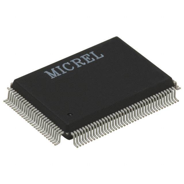
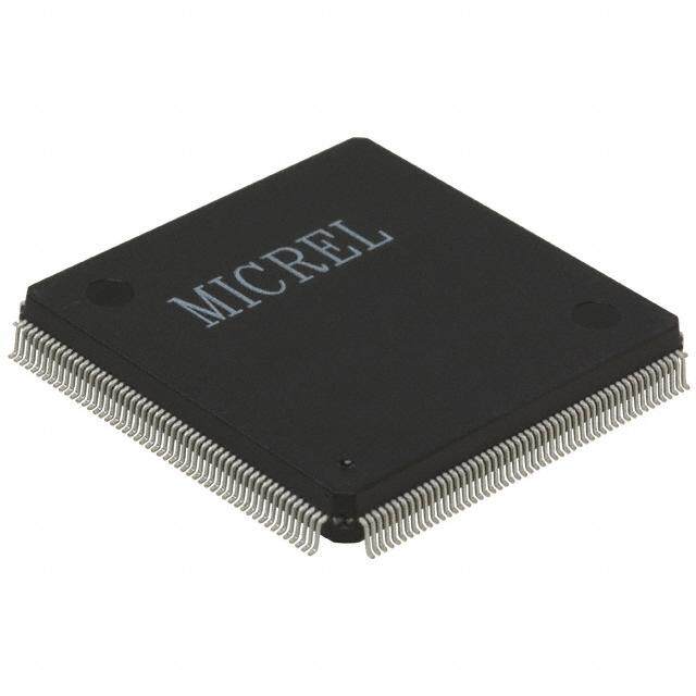
19-4835; 8/09 DS34T101, DS34T102, DS34T104, DS34T108 Single/Dual/Quad/Octal TDM-over-Packet Chip General Description Features These IETF PWE3 SAToP/CESoPSN/TDMoIP/HDLC Full-Featured IC Includes E1/T1 LIUs and compliant devices allow up to eight E1, T1 or serial Framers, TDMoP Engine, and 10/100 MAC streams or one high-speed E3, T3, STS-1 or serial Transport of E1, T1, E3, T3 or STS-1 TDM or stream to be transported transparently over IP, MPLS Other CBR Signals Over Packet Networks or Ethernet networks. Jitter and wander of recovered Full Support for These Mapping Methods: clocks conform to G.823/G.824, G.8261, and TDM SAToP, CESoPSN, TDMoIP AAL1, HDLC, specifications. TDM data is transported in up to 64 Unstructured, Structured, Structured with CAS individually configurable bundles. All standards- Adaptive Clock Recovery, Common Clock, based TDM-over-packet mapping methods are External Clock and Loopback Timing Modes supported except AAL2. Frame-based serial HDLC data flows are also supported. With built-in full- On-Chip TDM Clock Recovery Machines, One featured E1/T1 framers and LIUs. These ICs Per Port, Independently Configurable encapsulate the TDM-over-packet solution from Clock Recovery Algorithm Handles Network analog E1/T1 signal to Ethernet MII while preserving PDV, Packet Loss, Constant Delay Changes, options to make use of TDM streams at key Frequency Changes and Other Impairments intermediate points. The high level of integration 64 Independent Bundles/Connections available with the DS34T10x devices minimizes cost, Multiprotocol Encapsulation Supports IPv4, board space, and time to market. IPv6, UDP, RTP, L2TPv3, MPLS, Metro Ethernet VLAN Support According to 802.1p and 802.1Q Applications 10/100 Ethernet MAC Supports MII/RMII/SSMII TDM Circuit Extension Over PSN Selectable 32-Bit, 16-Bit or SPI Processor Bus o Leased-Line Services Over PSN Operates from Only Two Clock Signals, One for o TDM Over GPON/EPON Clock Recovery and One for Packet Processing o TDM Over Cable Glueless SDRAM Buffer Management o TDM Over Wireless Cellular Backhaul Over PSN Low-Power 1.8V Core, 3.3V I/O Multiservice Over Unified PSN See detailed feature list in Section 7. HDLC-Based Traffic Transport Over PSN Functional Diagram Ordering Information PART PORTS TEMP RANGE PIN-PACKAGE CPU B us DS34T101GN 1 -40C to +85C 484 TEBGA DS34T108 DS34T101GN+ 1 -40C to +85C 484 TEBGA Octal T rE a1n/sTc1e/Jiv1e r E mECnuirglcaiuntiieot n E1 t0h/e1r0n0 et xMII DDSS3344TT110022GGNN+ 22 --4400CC ttoo ++8855CC 448844 TTEEBBGGAA Framers MAC DS34T104GN 4 -40C to +85C 484 TEBGA IntEe1rf/aTc1e s B&LE ICURAsTS Buffer Clock DS34T104GN+ 4 -40C to +85C 484 TEBGA Manager Adapters DS34T108GN 8 -40C to +85C 484 HSBGA DS34T108GN+ 8 -40C to +85C 484 HSBGA TDM SDRAM Clock Inputs Access Interface +Denotes lead(Pb)-free/RoHS-compliant package (explanation). ________________________________________________________Maxim Integrated Products 1 Some revisions of this device may incorporate deviations from published specifications known as errata. Multiple revisions of any device may be simultaneously available through various sales channels. For information about device errata, go to: www.maxim-ic.com/errata. For pricing, delivery, and ordering information, please contact Maxim Direct at 1-888-629-4642, or visit Maxim’s website at www.maxim-ic.com.
____________________________________________________DS34T101, DS34T102, DS34T104, DS34T108 Table of Contents 1 INTRODUCTION...................................................................................................................................10 2 ACRONYMS AND GLOSSARY............................................................................................................10 3 APPLICABLE STANDARDS................................................................................................................13 4 DETAILED DESCRIPTION...................................................................................................................14 5 APPLICATION EXAMPLES .................................................................................................................16 6 BLOCK DIAGRAM................................................................................................................................18 7 FEATURES...........................................................................................................................................20 8 OVERVIEW OF MAJOR OPERATIONAL MODES..............................................................................25 8.1 INTERNAL MODE................................................................................................................................25 8.1.1 Internal One-Clock Mode...........................................................................................................................26 8.1.2 Internal Two-Clock Mode...........................................................................................................................26 8.2 EXTERNAL MODE..............................................................................................................................27 9 PIN DESCRIPTIONS.............................................................................................................................28 9.1 SHORT PIN DESCRIPTIONS................................................................................................................28 9.2 DETAILED PIN DESCRIPTIONS............................................................................................................30 10 FUNCTIONAL DESCRIPTION............................................................................................................44 10.1 POWER-SUPPLY CONSIDERATIONS..................................................................................................44 10.2 CPU INTERFACE.............................................................................................................................44 10.3 SPI INTERFACE...............................................................................................................................47 10.3.1 SPI Operation..........................................................................................................................................47 10.3.2 SPI Modes...............................................................................................................................................48 10.3.3 SPI Signals..............................................................................................................................................49 10.3.4 SPI Protocol.............................................................................................................................................49 10.4 CLOCK STRUCTURE.........................................................................................................................52 10.5 RESET AND POWER-DOWN..............................................................................................................53 10.6 TDM-OVER-PACKET BLOCK.............................................................................................................54 10.6.1 Packet Formats.......................................................................................................................................54 10.6.2 Typical Application...................................................................................................................................63 10.6.3 Clock Recovery.......................................................................................................................................65 10.6.4 Timeslot Assigner (TSA)..........................................................................................................................66 10.6.5 CAS Handler............................................................................................................................................67 10.6.6 AAL1 Payload Type Machine..................................................................................................................71 10.6.7 HDLC Payload Type Machine.................................................................................................................74 10.6.8 RAW Payload Type Machine..................................................................................................................75 10.6.9 SDRAM and SDRAM Controller..............................................................................................................79 10.6.10 Jitter Buffer Control (JBC).....................................................................................................................80 10.6.11 Queue Manager.....................................................................................................................................83 10.6.12 Ethernet MAC........................................................................................................................................95 10.6.13 Packet Classifier....................................................................................................................................98 10.6.14 Packet Trailer Support.........................................................................................................................101 10.6.15 Counters and Status Registers...........................................................................................................102 10.6.16 Connection Level Redundancy...........................................................................................................102 10.6.17 OAM Signaling.....................................................................................................................................103 10.7 GLOBAL RESOURCES....................................................................................................................104 10.8 PER-PORT RESOURCES................................................................................................................104 10.9 DEVICE INTERRUPTS.....................................................................................................................104 2 of 366
____________________________________________________DS34T101, DS34T102, DS34T104, DS34T108 10.9.1 TDMoP Interrupts..................................................................................................................................104 10.9.2 LIU, Framer and BERT Interrupts.........................................................................................................106 10.10 ELASTIC STORES AND FRAMER SYSTEM INTERFACE.....................................................................108 10.10.1 Elastic Store Initialization.....................................................................................................................108 10.10.2 Minimum Delay Mode..........................................................................................................................109 10.10.3 Additional Elastic Store Information....................................................................................................109 10.11 FRAMERS....................................................................................................................................111 10.11.1 T1 and E1 Framing Formats...............................................................................................................111 10.11.2 T1 Transmit Frame Synchronizer........................................................................................................115 10.11.3 Signaling..............................................................................................................................................115 10.11.4 T1 Datalink..........................................................................................................................................118 10.11.5 E1 Datalink..........................................................................................................................................120 10.11.6 Maintenance and Alarms.....................................................................................................................121 10.11.7 E1 Automatic Alarm Generation..........................................................................................................123 10.11.8 Error Count Registers..........................................................................................................................124 10.11.9 DS0 Monitoring Function.....................................................................................................................125 10.11.10 Framer and Payload Loopbacks.......................................................................................................126 10.11.11 Per-Channel Loopback......................................................................................................................126 10.11.12 Per-Channel Idle Code Insertion.......................................................................................................126 10.11.13 Digital Milliwatt Code Generation......................................................................................................127 10.11.14 In-Band Loop Code Generation and Detection (T1 Only).................................................................127 10.11.15 G.706 Intermediate CRC-4 Recalculation (E1 Only).........................................................................128 10.11.16 SLC–96 Operation (T1 Only).............................................................................................................128 10.12 HDLC CONTROLLERS.................................................................................................................129 10.12.1 Receive HDLC Controller....................................................................................................................130 10.12.2 Transmit HDLC Controller...................................................................................................................132 10.13 LINE INTERFACE UNITS (LIU).......................................................................................................134 10.13.1 LIU Operation......................................................................................................................................135 10.13.2 LIU Transmitter....................................................................................................................................136 10.13.3 LIU Receiver........................................................................................................................................138 10.13.4 Jitter Attenuator...................................................................................................................................140 10.13.5 LIU Loopbacks.....................................................................................................................................141 10.14 BIT ERROR RATE TEST FUNCTIONS (BERTS)...............................................................................144 10.14.1 BERT General Description..................................................................................................................144 10.14.2 BERT Features....................................................................................................................................144 10.14.3 BERT Configuration and Monitoring....................................................................................................144 10.14.4 BERT Receive Pattern Detection........................................................................................................145 10.14.5 BERT Transmit Pattern Generation....................................................................................................147 10.15 LIU - FRAMER CONNECTIONS......................................................................................................148 11 DEVICE REGISTERS.......................................................................................................................149 11.1 ADDRESSING.................................................................................................................................149 11.2 TOP-LEVEL MEMORY MAP.............................................................................................................150 11.3 GLOBAL REGISTERS......................................................................................................................151 11.4 TDM-OVER-PACKET REGISTERS....................................................................................................159 11.4.1 Configuration and Status Registers.......................................................................................................160 11.4.2 Bundle Configuration Tables.................................................................................................................174 11.4.3 Counters................................................................................................................................................184 11.4.4 Status Tables.........................................................................................................................................187 11.4.5 Timeslot Assignment Tables.................................................................................................................189 11.4.6 CPU Queues.........................................................................................................................................191 11.4.7 Transmit Buffers Pool............................................................................................................................196 11.4.8 Jitter Buffer Control................................................................................................................................197 11.4.9 Transmit Software CAS.........................................................................................................................201 11.4.10 Receive Line CAS...............................................................................................................................203 11.4.11 Clock Recovery...................................................................................................................................204 11.4.12 Receive SW Conditioning Octet Select...............................................................................................205 3 of 366
____________________________________________________DS34T101, DS34T102, DS34T104, DS34T108 11.4.13 Receive SW CAS................................................................................................................................206 11.4.14 Interrupt Controller...............................................................................................................................207 11.4.15 Packet Classifier..................................................................................................................................213 11.4.16 Ethernet MAC......................................................................................................................................214 11.5 FRAMER, LIU AND BERT REGISTERS.............................................................................................224 11.5.1 Receive Framer Registers.....................................................................................................................224 11.5.2 Transmit Formatter Registers................................................................................................................272 11.5.3 LIU Registers.........................................................................................................................................303 11.5.4 BERT Registers.....................................................................................................................................312 12 JTAG INFORMATION.......................................................................................................................320 13 DC ELECTRICAL CHARACTERISTICS..........................................................................................325 14 AC TIMING CHARACTERISTICS.....................................................................................................326 14.1 LIU CHARACTERISTICS..................................................................................................................326 14.2 LIU AND FRAMER TDM INTERFACE TIMING.....................................................................................327 14.3 CPU INTERFACE TIMING................................................................................................................330 14.4 SPI INTERFACE TIMING..................................................................................................................331 14.5 SDRAM INTERFACE TIMING..........................................................................................................332 14.6 TDM-OVER-PACKET TDM INTERFACE TIMING................................................................................335 14.7 ETHERNET MII/RMII/SSMII INTERFACE TIMING..............................................................................338 14.8 CLAD AND SYSTEM CLOCK TIMING................................................................................................340 14.9 JTAG INTERFACE TIMING..............................................................................................................341 15 APPLICATIONS................................................................................................................................342 15.1 CONNECTING A SERIAL INTERFACE TRANSCEIVER..........................................................................342 15.2 CONNECTING AN ETHERNET PHY OR MAC....................................................................................343 15.3 IMPLEMENTING CLOCK RECOVERY IN HIGH SPEED APPLICATIONS..................................................345 15.4 CONNECTING A MOTOROLA MPC860 PROCESSOR........................................................................345 15.4.1 Connecting the Bus Signals..................................................................................................................345 15.4.2 Connecting the H_READY_N Signal.....................................................................................................348 15.5 WORKING IN SPI MODE.................................................................................................................349 15.6 CONNECTING SDRAM DEVICES....................................................................................................349 16 PIN ASSIGNMENT............................................................................................................................350 16.1 BOARD DESIGN FOR MULTIPLE DS34T10X DEVICES......................................................................350 16.2 DS34T101 PIN ASSIGNMENT ........................................................................................................361 16.3 DS34T102 PIN ASSIGNMENT ........................................................................................................362 16.4 DS34T104 PIN ASSIGNMENT ........................................................................................................363 16.5 DS34T108 PIN ASSIGNMENT ........................................................................................................364 17 PACKAGE INFORMATION..............................................................................................................365 18 THERMAL INFORMATION...............................................................................................................365 19 DATA SHEET REVISION HISTORY.................................................................................................366 4 of 366
____________________________________________________DS34T101, DS34T102, DS34T104, DS34T108 List of Figures Figure 5-1. TDMoP in a Metropolitan Packet Switched Network..............................................................................16 Figure 5-2. TDMoP in Cellular Backhaul...................................................................................................................17 Figure 6-1. Top-Level Block Diagram........................................................................................................................18 Figure 6-2. TDM Cross-Connection Block Diagram..................................................................................................19 Figure 8-1. Internal Mode Block Diagram.................................................................................................................25 Figure 8-2. Internal One-Clock Mode.......................................................................................................................26 Figure 8-3. Internal Two Clock Mode (Framed)........................................................................................................27 Figure 8-4. Internal Two Clock Mode (Unframed)....................................................................................................27 Figure 10-1. CPU Interface Functional Diagram......................................................................................................44 Figure 10-2. Write Access, 32-Bit Bus......................................................................................................................45 Figure 10-3. Read Access, 32-Bit Bus......................................................................................................................46 Figure 10-4. Read/Write Access, 16-Bit Bus............................................................................................................46 Figure 10-5. Write Access to the SDRAM, 16-Bit Bus..............................................................................................47 Figure 10-6. Read Access to the SDRAM, 16-Bit Bus.............................................................................................47 Figure 10-7. SPI Interface with One Slave...............................................................................................................48 Figure 10-8. SPI Interface Timing, SPI_CP=0..........................................................................................................48 Figure 10-9. SPI Interface Timing, SPI_CP=1..........................................................................................................48 Figure 10-10. TDM-over-Packet Encapsulation Formats.........................................................................................55 Figure 10-11. Single VLAN Tag Format...................................................................................................................56 Figure 10-12. Stacked VLAN Tag Format................................................................................................................56 Figure 10-13. UDP/IPv4 Header Format..................................................................................................................56 Figure 10-14. UDP/IPv6 Header Format..................................................................................................................57 Figure 10-15. MPLS Header Format........................................................................................................................58 Figure 10-16. MEF Header Format...........................................................................................................................58 Figure 10-17. L2TPv3/IPv4 Header Format.............................................................................................................59 Figure 10-18. L2TPv3/IPv6 Header Format.............................................................................................................60 Figure 10-19. Control Word Format..........................................................................................................................60 Figure 10-20. RTP Header Format...........................................................................................................................61 Figure 10-21. VCCV OAM Packet Format................................................................................................................62 Figure 10-22. UDP/IP-Specific OAM Packet Format................................................................................................63 Figure 10-23. TDM Connectivity over a PSN...........................................................................................................64 Figure 10-24. TDMoP Packet Format in a Typical Application.................................................................................64 Figure 10-25. TDMoMPLS Packet Format in a Typical Application.........................................................................64 Figure 10-26. CAS Transmitted in the TDM-to-Ethernet Direction...........................................................................67 Figure 10-27. Transmit SW CAS Table Format for E1 and T1-ESF Interfaces........................................................68 Figure 10-28. Transmit SW CAS Table Format for T1-SF Interfaces......................................................................68 Figure 10-29. E1 MF Interface RSIG Timing Diagram (two_clocks=1)....................................................................68 Figure 10-30. T1 ESF Interface RSIG Timing Diagram (two_clocks=0)..................................................................69 Figure 10-31. T1 SF Interface RSIG (two_clocks=0) – Timing Diagram..................................................................69 Figure 10-32. CAS Transmitted in the Ethernet-to-TDM Direction...........................................................................70 Figure 10-33. E1 MF Interface TSIG Timing Diagram..............................................................................................71 Figure 10-34. T1 ESF Interface TSIG Timing Diagram............................................................................................71 Figure 10-35. T1 SF Interface TSIG Timing Diagram...............................................................................................71 Figure 10-36. AAL1 Mapping, General.....................................................................................................................72 Figure 10-37. AAL1 Mapping, Structured-Without-CAS Bundles.............................................................................73 Figure 10-38. HDLC Mapping...................................................................................................................................74 Figure 10-39. SAToP Unstructured Packet Mapping...............................................................................................75 Figure 10-40. CESoPSN Structured-Without-CAS Mapping....................................................................................76 Figure 10-41. CESoPSN Structured-With-CAS Mapping (No Frag, E1 Example)...................................................76 Figure 10-42. CESoPSN Structured-With-CAS Mapping (No Frag, T1-ESF Example)...........................................77 Figure 10-43. CESoPSN Structured-With-CAS Mapping (No Frag, T1-SF Example).............................................77 Figure 10-44. CESoPSN Structured-With-CAS Mapping (Frag, E1 Example)........................................................78 Figure 10-45. SDRAM Access through the SDRAM Controller................................................................................80 Figure 10-46. Loop Timing in TDM Networks...........................................................................................................80 Figure 10-47. Timing in TDM-over-Packet...............................................................................................................81 5 of 366
____________________________________________________DS34T101, DS34T102, DS34T104, DS34T108 Figure 10-48. Jitter Buffer Parameters.....................................................................................................................82 Figure 10-49. TDM-over-Packet Data Flow Diagram...............................................................................................84 Figure 10-50. Free Buffer Pool Operation................................................................................................................88 Figure 10-51. TDM-to-Ethernet Flow........................................................................................................................89 Figure 10-52. Ethernet-to-TDM Flow........................................................................................................................90 Figure 10-53. TDM-to-TDM Flow..............................................................................................................................91 Figure 10-54. TDM-to-CPU Flow..............................................................................................................................92 Figure 10-55. CPU-to-TDM Flow..............................................................................................................................93 Figure 10-56. CPU-to-Ethernet Flow........................................................................................................................94 Figure 10-57. Ethernet-to-CPU Flow........................................................................................................................95 Figure 10-58. Ethernet MAC.....................................................................................................................................96 Figure 10-59. Format of TDMoIP Packet with VLAN Tag.........................................................................................99 Figure 10-60. Format of TDMoMPLS Packet with VLAN Tag..................................................................................99 Figure 10-61. Format of TDMoMEF Packet with VLAN Tag....................................................................................99 Figure 10-62. Structure of Packets with Trailer......................................................................................................102 Figure 10-63. Interrupt Pin Logic............................................................................................................................105 Figure 10-64. LIU, Framer and BERT Interrupt Information Flow Diagram............................................................107 Figure 10-65. CRC-4 Recalculate Method.............................................................................................................128 Figure 10-66. Receive HDLC Servicing Example...................................................................................................131 Figure 10-67. Transmit HDLC Servicing Example..................................................................................................133 Figure 10-68. LIU External Components, Longitudinal Protection.........................................................................134 Figure 10-69. T1/J1 Transmit Pulse Templates.....................................................................................................137 Figure 10-70. E1 Transmit Pulse Templates..........................................................................................................137 Figure 10-71. Typical Rx Monitor Application.........................................................................................................138 Figure 10-72. Jitter Tolerance, T1 Mode................................................................................................................139 Figure 10-73. Jitter Tolerance, E1 and 2048kHz Modes........................................................................................139 Figure 10-74. Jitter Attenuation..............................................................................................................................141 Figure 10-75. Analog Loopback..............................................................................................................................141 Figure 10-76. Local Loopback................................................................................................................................142 Figure 10-77. Remote Loopback............................................................................................................................142 Figure 10-78. Dual Loopback.................................................................................................................................143 Figure 10-79. PRBS Synchronization State Diagram.............................................................................................146 Figure 10-80. Repetitive Pattern Synchronization State Diagram..........................................................................147 Figure 10-81. LIU + Framer Connections...............................................................................................................148 Figure 11-1. 16-Bit Addressing...............................................................................................................................149 Figure 11-2. 32-Bit Addressing...............................................................................................................................149 Figure 11-3. Partial Data Elements (shorter than 16 bits)......................................................................................149 Figure 11-4. Partial Data Elements (16 to 32 bits long)..........................................................................................150 Figure 12-1. JTAG Block Diagram..........................................................................................................................320 Figure 12-2. JTAG TAP Controller State Machine.................................................................................................321 Figure 14-1. Receive Framer Timing Using the RCLKF Pin...................................................................................327 Figure 14-2. Receive Framer Timing Using the RCLK Pin.....................................................................................328 Figure 14-3. Receive Framer Timing, Elastic Store Enabled.................................................................................328 Figure 14-4. Receive Framer Timing, Line Side with LIU Not Used.......................................................................328 Figure 14-5. Transmit Formatter Timing Using the TCLKF Pin..............................................................................329 Figure 14-6. Transmit Formatter Timing, Elastic Store Enabled............................................................................330 Figure 14-7. Transmit Formatter Timing, Line Side with LIU Not Used..................................................................330 Figure 14-8. RST_SYS_N Timing...........................................................................................................................330 Figure 14-9. CPU Interface Write Cycle Timing.....................................................................................................331 Figure 14-10. CPU Interface Read Cycle Timing...................................................................................................331 Figure 14-11. SPI interface Timing (SPI_CP = 0)...................................................................................................332 Figure 14-12. SPI interface Timing (SPI_CP = 1)...................................................................................................332 Figure 14-13. SDRAM Interface Write Cycle Timing..............................................................................................333 Figure 14-14. SDRAM Interface Read Cycle Timing..............................................................................................334 Figure 14-15. TDMoP TDM Timing, One-Clock Mode (Two_clocks=0, Tx_sample=1).........................................335 Figure 14-16. TDMoP TDM Timing, One Clock Mode (Two_clocks=0, Tx_sample=0).........................................336 Figure 14-17. TDMoP TDM Timing, Two Clock Mode (Two_clocks=1, Tx_sample=1, Rx_sample=1).................336 Figure 14-18. TDMoP TDM Timing, Two Clocks Mode (Two_clocks=1, Tx_sample=0, Rx_sample=0)...............336 6 of 366
____________________________________________________DS34T101, DS34T102, DS34T104, DS34T108 Figure 14-19. TDMoP TDM Timing, Two Clocks Mode (Two_clocks=1, Tx_sample=0, Rx_sample=1)...............337 Figure 14-20. TDMoP TDM Timing, Two Clocks Mode (Two_clocks=1, Tx_sample=1, Rx_sample=0)...............337 Figure 14-21. MII Management Interface Timing...................................................................................................338 Figure 14-22. MII Interface Output Signal Timing...................................................................................................338 Figure 14-23. MII Interface Input Signal Timing.....................................................................................................339 Figure 14-24. RMII Interface Output Signal Timing................................................................................................339 Figure 14-25. RMII Interface Input Signal Timing...................................................................................................339 Figure 14-26. SSMII Interface Output Signal Timing..............................................................................................340 Figure 14-27. SSMII Interface Input Signal Timing.................................................................................................340 Figure 14-28. JTAG Interface Timing Diagram.......................................................................................................341 Figure 15-1. Connecting Port 1 to a Serial Transceiver.........................................................................................342 Figure 15-2. Connecting the Ethernet Port to a PHY in MII Mode.........................................................................343 Figure 15-3. Connecting the Ethernet Port to a MAC in MII Mode.........................................................................343 Figure 15-4. Connecting the Ethernet Port to a PHY in RMII Mode.......................................................................343 Figure 15-5. Connecting the Ethernet Port to a MAC in RMII Mode......................................................................344 Figure 15-6. Connecting the Ethernet Port to a PHY in SSMII Mode.....................................................................344 Figure 15-7. Connecting the Ethernet Port to a MAC in SSMII Mode....................................................................344 Figure 15-8. External Clock Multiplier for High Speed Applications.......................................................................345 Figure 15-9. 32-Bit CPU Bus Connections.............................................................................................................346 Figure 15-10. 16-Bit CPU Bus Connections...........................................................................................................347 Figure 15-11. Connecting the H_READY_N Signal to the MPC860 TA Pin.........................................................348 Figure 15-12. Internal CPLD Logic to Synchronize H_READY_N to the MPC860 Clock......................................348 Figure 16-1. DS34T101 Pin Assignment (TE-CSBGA Package)...........................................................................361 Figure 16-2. DS34T102 Pin Assignment (TE-CSBGA Package)...........................................................................362 Figure 16-3. DS34T104 Pin Assignment (TE-CSBGA Package)...........................................................................363 Figure 16-4. DS34T108 Pin Assignment (HSBGA Package).................................................................................364 List of Tables Table 3-1. Applicable Standards...............................................................................................................................13 Table 9-1. Short Pin Descriptions.............................................................................................................................28 Table 9-2. Internal E1/T1 LIU Line Interface Pins....................................................................................................30 Table 9-3. External E1/T1 LIU Line Interface Pins...................................................................................................31 Table 9-4. Framer TDM Interface Pins.....................................................................................................................32 Table 9-5. TDM-over-Packet Engine TDM Interface Pins........................................................................................34 Table 9-6. SDRAM Interface Pins.............................................................................................................................36 Table 9-7. Ethernet PHY Interface Pins (MII/RMII/SSMII)........................................................................................37 Table 9-8. Global Clock Pins....................................................................................................................................39 Table 9-9. CPU Interface Pins..................................................................................................................................40 Table 9-10. JTAG Interface Pins..............................................................................................................................42 Table 9-11. Reset and Factory Test Pins.................................................................................................................42 Table 9-12. Power and Ground Pins........................................................................................................................43 Table 10-1. CPU Data Bus Widths...........................................................................................................................45 Table 10-2. SPI Write Command Sequence............................................................................................................50 Table 10-3. SPI_ Read Command Sequence..........................................................................................................51 Table 10-4. SPI Status Command Sequence...........................................................................................................52 Table 10-5. Reset Functions.....................................................................................................................................53 Table 10-6. Ethernet Frame Fields...........................................................................................................................55 Table 10-7. IPv4 Header Fields (UDP).....................................................................................................................57 Table 10-8. UDP Header Fields................................................................................................................................57 Table 10-9. IPv6 Header Fields (UDP).....................................................................................................................58 Table 10-10. MPLS Header Fields...........................................................................................................................58 Table 10-11. MEF Header Fields..............................................................................................................................58 Table 10-12. IPv4 Header Fields (L2TPv3)..............................................................................................................59 Table 10-13. L2TPv3 Header Fields.........................................................................................................................59 7 of 366
____________________________________________________DS34T101, DS34T102, DS34T104, DS34T108 Table 10-14. IPv6 Header Fields (L2TPv3)..............................................................................................................60 Table 10-15. Control Word Fields.............................................................................................................................60 Table 10-16. RTP Header Fields..............................................................................................................................61 Table 10-17. VCCV OAM Payload Fields.................................................................................................................62 Table 10-18. UDP/IP-Specific OAM Payload Fields.................................................................................................63 Table 10-19. CAS – Supported Interface Connections for AAL1 and CESoPSN....................................................68 Table 10-20. CAS Handler Selector Decision Logic.................................................................................................69 Table 10-21. AAL1 Header Fields............................................................................................................................72 Table 10-22. SDRAM Access Resolution.................................................................................................................79 Table 10-23. SDRAM CAS Latency vs. Frequency..................................................................................................79 Table 10-24. Buffer Descriptor First Dword Fields (Used for all Paths)...................................................................85 Table 10-25. Buffer Descriptor Second Dword Fields (TDM ETH and CPU ETH)..........................................86 Table 10-26. Buffer Descriptor Second Dword Fields (ETH CPU)......................................................................86 Table 10-27. Buffer Descriptor Third Dword Fields (ETH CPU)..........................................................................87 Table 10-28. Start of an 802.3 Pause Packet...........................................................................................................97 Table 10-29. Handling IPv4 and IPv6 Packets.........................................................................................................98 Table 10-30. TDMoIP Port Number Comparison for TDMoIP Packet Classification.............................................100 Table 10-31. Bundle Identifier Location and Width.................................................................................................100 Table 10-32. Registers Related to the Elastic Store...............................................................................................108 Table 10-33. Elastic Store Delay After Initialization................................................................................................109 Table 10-34. T1-SF Framing Pattern and Signaling Bits........................................................................................111 Table 10-35. T1-ESF Framing Pattern and Signaling Bits.....................................................................................112 Table 10-36. SLC-96 Framing Pattern and Signaling Bits.....................................................................................112 Table 10-37. E1 CRC-4 Multiframe Framing Pattern.............................................................................................114 Table 10-38. Registers Related to Setting Up the Framer and Formatter..............................................................114 Table 10-39. Registers Related to the Transmit Synchronizer...............................................................................115 Table 10-40. Registers Related to Signaling..........................................................................................................116 Table 10-41. Timeslot Number Schemes...............................................................................................................116 Table 10-42. Registers Related to T1 Transmit BOC.............................................................................................118 Table 10-43. Registers Related to T1 Receive BOC..............................................................................................119 Table 10-44. Registers Related to Legacy T1 Transmit FDL.................................................................................119 Table 10-45. Registers Related to Legacy T1 Receive FDL..................................................................................119 Table 10-46. Registers Related to Maintenance and Alarms.................................................................................121 Table 10-47. T1 Alarm Criteria...............................................................................................................................122 Table 10-48. E1 Alarm Criteria...............................................................................................................................123 Table 10-49. E1 LOF Sync and Resync Criteria....................................................................................................123 Table 10-50. T1 Line Code Violation Counting Options.........................................................................................124 Table 10-51. E1 Line Code Violation Counting Options.........................................................................................124 Table 10-52. T1 Path Code Violation Counting Options.........................................................................................125 Table 10-53. T1 Frames Out Of Sync Counting Options........................................................................................125 Table 10-54. Registers Related to DS0 Monitoring................................................................................................125 Table 10-55. Registers Related to Framer and Payload Loopbacks......................................................................126 Table 10-56. Registers Related to T1 In-Band Loop Code Generator...................................................................127 Table 10-57. Registers Related to T1 In-Band Loop Code Detection....................................................................128 Table 10-58. Registers Related to SLC96..............................................................................................................128 Table 10-59. LIU External Components.................................................................................................................134 Table 10-60. Transformer Specifications................................................................................................................135 Table 10-61. Pseudorandom Pattern Generation...................................................................................................145 Table 10-62. Repetitive Pattern Generation...........................................................................................................145 Table 11-1. Top-Level Memory Map.......................................................................................................................150 Table 11-2. Global Registers..................................................................................................................................151 Table 11-3. TDMoP Memory Map..........................................................................................................................159 Table 11-4. TDMoP Configuration Registers..........................................................................................................160 Table 11-5. TDMoP Status Registers.....................................................................................................................160 Table 11-6. Counters Types...................................................................................................................................184 Table 11-7. CPU Queues.......................................................................................................................................191 Table 11-8. Jitter Buffer Status Table.....................................................................................................................197 Table 11-9. Bundle Timeslot Table.........................................................................................................................197 8 of 366
____________________________________________________DS34T101, DS34T102, DS34T104, DS34T108 Table 11-10. Transmit Software CAS Registers.....................................................................................................201 Table 11-11. Receive Line CAS Registers.............................................................................................................203 Table 11-12. Clock Recovery Registers.................................................................................................................204 Table 11-13. Receive SW Conditioning Octet Select Registers.............................................................................205 Table 11-14. Receive SW CAS Registers..............................................................................................................206 Table 11-15. Interrupt Controller Registers............................................................................................................207 Table 11-16. Packet Classifier OAM Identification Registers.................................................................................213 Table 11-17. Ethernet MAC Registers....................................................................................................................214 Table 11-18. Ethernet MAC Counters....................................................................................................................219 Table 11-19. Framer, LIU, BERT Memory Map......................................................................................................224 Table 11-20. Receive Framer Registers.................................................................................................................224 Table 11-21. Transmit Formatter Registers............................................................................................................272 Table 11-22. LIU Registers.....................................................................................................................................303 Table 11-23. BERT Registers.................................................................................................................................312 Table 12-1. JTAG Instruction Codes......................................................................................................................323 Table 12-2. JTAG ID Code.....................................................................................................................................323 Table 13-1. Recommended DC Operating Conditions...........................................................................................325 Table 13-2. DC Electrical Characteristics...............................................................................................................325 Table 14-1. Input Pin Transition Time Requirements.............................................................................................326 Table 14-2. Transmitter Characteristics.................................................................................................................326 Table 14-3. Receiver AC Characteristics...............................................................................................................327 Table 14-4. Transmit AC Characteristics................................................................................................................329 Table 14-5. CPU Interface AC characteristics........................................................................................................330 Table 14-6. SPI Interface AC Characteristics.........................................................................................................331 Table 14-7. SDRAM Interface AC Characteristics..................................................................................................332 Table 14-8. TDMoP TDM Interface AC Characteristics..........................................................................................335 Table 14-9. TDMoP TDM Clock AC Characteristics...............................................................................................335 Table 14-10. MII Management Interface AC Characteristics.................................................................................338 Table 14-11. MII Interface AC Characteristics........................................................................................................338 Table 14-12. MII Clock Timing................................................................................................................................338 Table 14-13. RMII Interface AC Characteristics.....................................................................................................339 Table 14-14. RMII Clock Timing.............................................................................................................................339 Table 14-15. SSMII Interface AC Characteristics...................................................................................................339 Table 14-16. SSMII Clock Timing...........................................................................................................................339 Table 14-17. CLAD1 and CLAD2 Input Clock Specifications.................................................................................340 Table 14-18. JTAG Interface Timing.......................................................................................................................341 Table 15-1. SPI Mode I/O Connections..................................................................................................................349 Table 15-2. List of Suggested SDRAM Devices.....................................................................................................349 Table 16-1. Common Board Design Connections..................................................................................................350 9 of 366
____________________________________________________DS34T101, DS34T102, DS34T104, DS34T108 1 Introduction The DS34T101/2/4/8 family of products combine E1/T1 LIUs and framers and TDM-over-packet circuit emulation circuitry into one die. Dedicated payload-type engines are included for TDMoIP (AAL1), CESoPSN, SAToP, and HDLC. Products in the DS34T10x family provide the mapping/demapping capability to enable the transport of TDM data (Nx64kbps, E1, T1, J1, E3, T3, STS-1) or other constant bit-rate data over IP, MPLS or Ethernet networks. These products enable service providers to migrate to next generation networks while continuing to provide legacy voice, data and leased-line services. They allow enterprises to transport voice and video over the same IP/Ethernet network that is currently used only for LAN traffic, thereby minimizing network maintenance and operating costs. Packet-switched networks, such as IP networks, were not designed to transport TDM data and have no inherent clock distribution mechanism. Therefore, when transporting TDM data over packet switched networks, the TDM demapping function needs to accurately reconstruct the TDM service clock(s). The DS34T10x devices perform this important clock recovery task, creating recovered clocks with jitter and wander levels that conform to ITU-T G.823/824 and G.8261, even for networks which introduce significant packet delay variation and packet loss. The circuit emulation technology in the DS34T10x products that makes this possible is called TDM-over-Packet (TDMoP) and complements VoIP in those cases where VoIP is not applicable or where VoIP price/performance is not sufficient. Most importantly, TDMoP technology provides higher voice quality with lower latency than VoIP. Unlike VoIP, TDMoP can support all applications that run over E1/T1 circuits, not just voice. TDMoP can also provide traditional leased-line services over IP and is transparent to protocols and signaling. Because TDMoP provides an evolutionary, as opposed to revolutionary approach, investment protection is maximized. 2 Acronyms and Glossary Acronyms AAL1 ATM Adaptation Layer Type 1 AAL2 ATM Adaptation Layer Type 2 ATM Asynchronous Transfer Mode BGA Ball Grid Array BW Bandwidth CAS Channel Associated Signaling CBR Constant Bit-Rate CCS Common channel signaling CE Customer Edge CESoP Circuit Emulation Service over Packet CESoPSN Circuit Emulation Services over Packet Switched Network CLAD Clock Rate Adapter CPE Customer Premises Equipment CSMA Carrier Sense Multiple Access CSMA/CD Carrier Sense Multiple Access with Collision Detection DS0 Digital Signal Level 0 DS1 Digital Signal Level 1 DS3 Digital Signal Level 3 HDLC High-Level data Link Control IEEE Institute of Electrical and Electronics Engineers IETF Internet Engineering Task Force IP Internet Protocol JBC Jitter Buffer Control IWF Interworking Function LAN Local Area Network 10 of 366
____________________________________________________DS34T101, DS34T102, DS34T104, DS34T108 LIU Line Interface Unit LOF Loss of Frame (i.e. loss of frame alignment) LOS Loss of Signal MAC Media Access Control MEF Metro Ethernet Forum MFA MPLS / Frame Relay Alliance (Now called IP/MPLS Forum) MII Medium Independent Interface MPLS MULTI PROTOCOL LABEL SWITCHING OC-3 Optical Carrier Level 3 OCXO Oven Controlled Crystal Oscillator OFE Optical Front End OSI Open Systems Interconnection OSI-RM Open Systems Interconnection—Reference Model PDU Protocol Data Unit PDV Packet Delay Variation PE Provider Edge PRBS Pseudo-Random Bit Sequence PSN Packet Switched Network PSTN Public Switched Telephone Network PWE3 Pseudo-Wire Emulation Edge-to-Edge QoS Quality of Service RMII Reduced Medium Independent Interface Rx or RX Receive SAR Segmentation and Reassembly SAToP Structure-Agnostic TDM over Packet SDH Synchronous Digital Hierarchy SMII Serial Media Independent Interface SN Sequence Number SONET Synchronous Optical Network SS7 Signaling System 7 SSMII Source Synchronous Serial Media Independent Interface STM-1 Synchronous Transport Module Level 1 TDM Time Division Multiplexing TDMoIP TDM over Internet Protocol TDMoP TDM over Packet TSA Timeslot Assigner Tx or TX Transmit UDP User Datagram Protocol VoIP Voice over IP VPLS Virtual Private LAN Services WAN Wide Area Network 11 of 366
____________________________________________________DS34T101, DS34T102, DS34T104, DS34T108 Glossary BERT – Bit Error Rate Tester, a function used to test the integrity of a data link. A two-block set consisting of a Tx BERT that generates pseudo-random or repetitive patterns and optionally inserts bit errors into the sequence, and an Rx BERT that synchronizes to an incoming pattern and count bit errors. bundle – a virtual path configured at two endpoint TDMoP gateways to carry TDM or constant bit-rate data over a PSN. CLAD – Clock Rate Adapter, an analog PLL that creates an output clock signal that is phase/frequency locked to an input clock signal of a different frequency. A CLAD is said to “convert” one frequency to another or “adapt” (change) a clock’s rate to be a frequency that is useful to some other block on the chip. dword – a 32-bit (4-byte) unit of information (also known as a doubleword) framer – (1) a digital block that finds E1/T1 frame alignment in an incoming serial data stream and provides various types of status and alarm information about the signaling including loss-of-signal, loss-of-frame, frame bit errors, etc. Also known as a receive framer. (2) The word framer is also used generically to stand for the bidirectional block composed of a receive framer and a transmit formatter. formatter – a digital block that generates a serial data stream composed of successive E1/T1 frames (and optionally multiframes) filled with TDM data provided by the system. Also known as a transmit formatter. transceiver – a transmitter/receiver, which for E1/T1 typically means a block containing a receive framer, a transmit formatter, an LIU receiver and an LIU transmitter. E.g., DS34T108 has eight built-in E1/T1 transceivers. 12 of 366
____________________________________________________DS34T101, DS34T102, DS34T104, DS34T108 3 Applicable Standards Table 3-1. Applicable Standards SPECIFICATION SPECIFICATION TITLE ANSI T1.102 Digital Hierarchy—Electrical Interfaces, 1993 T1.107 Digital Hierarchy—Formats Specification, 1995 T1.231.02 Digital Hierarchy—Layer 1 In-Service Digital Transmission Performance Monitoring, 2003 T1.403 Network and Customer Installation Interfaces—DS1 Electrical Interface, 1999 AT&T Requirements for Interfacing Digital Terminal Equipment to Services Employing the Extended TR54016 Superframe Format (9/1989) TR62411 ACCUNET® T1.5 Service Description and Interface Specification (12/1990) ETSI Integrated Services Digital Network (ISDN); Primary rate User Network Interface (UNI); Part ETS 300 011 1: Layer 1 Specification V1.2.2 (2000-05) Transmission and Multiplexing (TM); Physical and Electrical Characteristics of Hierarchical ETS 300 166 Digital Interfaces for Equipment Using the 2 048 kbit/s - Based Plesiochronous or Synchronous Digital Hierarchies V1.2.1 (2001-09) Integrated Services Digital Network (ISDN);Access Digital Section for ISDN Primary Rate, ETS 300 233 ed.1 (1994-05) IEEE Carrier Sense Multiple Access with Collision Detection (CSMA/CD) Access Method and IEEE 802.3 Physical Layer Specifications (2005) IEEE 1149.1 Standard Test Access Port and Boundary-Scan Architecture, 1990 IETF RFC 4553 Structure-Agnostic Time Division Multiplexing (TDM) over Packet (SAToP) (06/2006) Encapsulation Methods for Transport of PPP/High-Level Data Link Control (HDLC) over RFC 4618 MPLS Networks (09/2006) Structure-Aware Time Division Multiplexed (TDM) Circuit Emulation Service over Packet RFC 5086 Switched Network (CESoPSN) (12/2007) RFC 5087 Time Division Multiplexing over IP (TDMoIP) (12/2007) ITU-T G.703 Physical/Electrical Characteristics of Hierarchical Digital Interfaces (11/2001) Synchronous Frame Structures Used at 1544, 6312, 2048, 8448 and 44736 kbit/s G.704 Hierarchical Levels (10/1998) Frame Alignment and Cyclic Redundancy Check (CRC) Procedures Relating to Basic Frame G.706 Structures Defined in Recommendation G.704 (1991) G.732 Characteristics of Primary PCM Multiplex Equipment Operating at 2048Kbit/s (11/1988) Characteristics of Synchronous Digital Multiplex Equipment Operating at 2048Kbit/s G.736 (03/1993) Loss of Signal (LOS) and Alarm Indication Signal (AIS) and Remote Defect Indication (RD) G.775 Defect Detection and Clearance Criteria for PDH Signals (10/1998) The Control of Jitter and Wander within Digital Networks which are Based on the 2048kbps G.823 Hierarchy (03/2000) The Control of Jitter and Wander within Digital Networks which are Based on the 1544kbps G.824 Hierarchy (03/2000) G.8261/Y.1361 Timing and Synchronization Aspects in Packet Networks (05/2006) I.363.1 B-ISDN ATM Adaptation Layer Specification: Type 1 AAL (08/1996) I.363.2 B-ISDN ATM Adaptation Layer Specification: Type 2 AAL (11/2000) I.366.2 AAL Type 2 Service Specific Convergence Sublayer for Narrow-Band Services (11/2000) I.431 Primary Rate User-Network Interface - Layer 1 Specification (03/1993) I.432 B-ISDN User-Network Interface – Physical Layer Specification (03/1993) O.151 Error Performance Measuring Equipment Operating at the Primary Rate and Above (1992) 13 of 366
____________________________________________________DS34T101, DS34T102, DS34T104, DS34T108 SPECIFICATION SPECIFICATION TITLE O.161 In-Service Code Violation Monitors for Digital Systems (1993) Y.1413 TDM-MPLS Network Interworking – User Plane Interworking (03/2004) Y.1414 Voice Services–MPLS Network Interworking (07/2004) Y.1452 Voice Trunking over IP Networks (03/2006) Y.1453 TDM-IP Interworking – User Plane Networking (03/2006) MEF Implementation Agreement for the Emulation of PDH Circuits over Metro Ethernet Networks MEF 8 (10/2004) MFA MFA 4.0 TDM Transport over MPLS Using AAL1 (06/2003) MFA 5.0.0 I.366.2 Voice Trunking Format over MPLS Implementation Agreement (08/2003) Emulation of TDM Circuits over MPLS Using Raw Encapsulation – Implementation MFA 8.0.0 Agreement (11/2004) 4 Detailed Description The DS34T108 is an 8-port device integrating a sophisticated multiport TDM-over-Packet (TDMoP) core and eight full-featured, independent, software-configurable E1/T1 transceivers. The DS34T104, DS34T102 and DS34T101 have the same functionality as the DS34T108, except they have only 4, 2 or 1 ports and transceivers, respectively. Each E1/T1 transceiver is composed of a line interface unit (LIU), a framer, an elastic store, an HDLC controller and a bit error rate tester (BERT) block. These transceivers connect seamlessly to the TDMoP block to form a complete solution for mapping and demapping E1/T1 to and from IP, MPLS or Ethernet networks. A MAC built into the TDMoP block supports connectivity to a single 10/100 Mbps PHY over an MII, RMII or SSMII interface. The DS34T10x devices are controlled through a 16 or 32-bit parallel bus interface or a high-speed SPI serial interface. TDM-over-Packet Core The TDM-over-Packet (TDMoP) core is the enabling block for circuit emulation and other network applications. It performs transparent transport of legacy TDM traffic over Packet Switched-Networks (PSN). The TDMoP core implements payload mapping methods such as AAL1 for circuit emulation, HDLC method, structure-agnostic SAToP method, and the structure-aware CESoPSN method. The AAL1 payload-type machine maps and demaps E1, T1, E3, T3, STS-1 and other serial data flows into and out of IP, MPLS or Ethernet packets, according to the methods described in ITU-T Y.1413, Y.1453, MEF 8, MFA 4.1 and IETF RFC 5087 (TDMoIP). It supports E1/T1 structured mode with or without CAS, using a timeslot size of 8 bits, or unstructured mode (carrying serial interfaces, unframed E1/T1 or E3/T3/STS-1 traffic). The HDLC payload-type machine maps and demaps HDLC dataflows into and out of IP/MPLS packets according to IETF RFC 4618 (excluding clause 5.3 – PPP) and IETF RFC 5087 (TDMoIP). It supports 2-, 7- and 8-bit timeslot resolution (i.e. 16, 56, and 64 kbps respectively), as well as N × 64 kbps bundles (n=1 to 32). Supported applications of this machine include trunking of HDLC-based traffic (such as Frame Relay) implementing Dynamic Bandwidth Allocation over IP/MPLS networks and HDLC-based signaling interpretation (such as ISDN D-channel signaling termination – BRI or PRI, V5.1/2, or GR-303). The SAToP payload-type machine maps and demaps unframed E1, T1, E3 or T3 data flows into and out of IP, MPLS or Ethernet packets according to ITU-T Y.1413, Y.1453, MEF 8, MFA 8.0.0 and IETF RFC 4553. It supports E1/T1/E3/T3 with no regard for the TDM structure. If TDM structure exists it is ignored, allowing this to be the simplest mapping/demapping method. The size of the payload is programmable for different services. This emulation suits applications where the provider edges have no need to interpret TDM data or to participate in the TDM signaling. The PSN network must have almost no packet loss and very low packet delay variation (PDV) for this method. The CESoPSN payload-type machine maps and demaps structured E1, T1, E3 or T3 data flows into and out of IP, MPLS or Ethernet packets with static assignment of timeslots inside a bundle according to ITU-T Y.1413, Y.1453, 14 of 366
____________________________________________________DS34T101, DS34T102, DS34T104, DS34T108 MEF 8, MFA 8.0.0 and the IETF RFC 5086 (CESoPSN). It supports E1/T1/E3/T3 while taking into account the TDM structure. The level of structure must be chosen for proper payload conversion such as the framing type (i.e. frame or multiframe). This method is less sensitive to PSN impairments but lost packets could still cause service interruption. E1/T1 Transceivers The LIU in each transceiver is composed of a transmitter, a receiver and a jitter attenuator. Internal software configurable impedance matching is provided for both transmit and receive paths, reducing external component count. The transmit interface is responsible for generating the necessary waveshapes for driving the E1/T1 twisted pair or coax cable and providing the correct source impedance depending on the type of cable used. T1 waveform generation includes DSX–1 line build-outs as well as CSU line build-outs of 0dB, -7.5dB, -15dB, and -22.5dB. E1 waveform generation includes G.703 waveshapes for both 75 coax and 120 twisted cables. The receive interface provides the correct line termination and recovers clock and data from the incoming line. The receive sensitivity adjusts automatically to the incoming signal level and can be programmed for 0dB to -43dB or 0dB to -12dB for E1 applications and 0dB to -15dB or 0dB to -36dB for T1 applications. The jitter attenuator removes phase jitter from the transmitted or received signal. The crystal-less jitter attenuator can be placed in either the transmit or receive path and requires only a T1- or E1-rate reference clock, which is typically synthesized by the CLAD1 block from a common reference frequency of 10MHz, 19.44MHz, 38.88MHz or 77.76MHz. In the framer block, the transmit formatter takes data from the TDMoP core, inserts the appropriate framing patterns and alarm information, calculates and inserts CRC codes, and provides the HDB3 or B8ZS encoding (zero code suppression) and AMI line coding. The receive framer decodes AMI, HDB3 and B8ZS line coding, finds frame and multiframe alignment in the incoming data stream, reports alarm information, counts framing/coding/CRC errors, and provides clock, data, and frame-sync signals to the TDMoP core. Both transmit and receive paths have built-in HDLC controller and BERT blocks. The HDLC blocks can be assigned to any timeslot, a portion of a timeslot or to the FDL (T1) or Sa bits (E1). Each controller has 64-byte FIFOs, reducing the amount of processor overhead required to manage the flow of data. The BERT blocks can generate and synchronize with pseudo-random and repetitive patterns, insert errors (singly or at a constant error rate) and detect and count errors to calculate bit error rates. 15 of 366
____________________________________________________DS34T101, DS34T102, DS34T104, DS34T108 5 Application Examples In Figure 5-1, a DS34T10x device is used in each TDMoP gateway to map TDM services into a packet-switched metropolitan network. TDMoP data is carried over various media: fiber, wireless, G/EPON, coax, etc. Figure 5-1. TDMoP in a Metropolitan Packet Switched Network 16 of 366
____________________________________________________DS34T101, DS34T102, DS34T104, DS34T108 Figure 5-2. TDMoP in Cellular Backhaul Other Possible Applications Point-to-Multipoint TDM Connectivity over IP/Ethernet The DS34T10x devices support NxDS0 TDMoP connections (known as bundles) with or without CAS (Channel Associated Signaling). There is no need for an external TDM cross-connect, since the packet domain can be used as a virtual cross-connect. Any bundle of timeslots can be directed to another remote location on the packet domain. HDLC Transport over IP/MPLS TDM traffic streams often contain HDLC-based control channels and data traffic. These data streams, when transported over a packet domain, should be treated differently than the time-sensitive TDM payload. DS34T10x devices can terminate HDLC channels in the TDM streams and optionally map them into IP/MPLS/Ethernet for transport. All HDLC-based control protocols (ISDN BRI and PRI, SS7 etc.) and all HDLC data traffic can be managed and transported. Using a Packet Backplane for Multiservice Concentrators A communications device with all the above-mentioned capabilities can use a packet-based backplane instead of the more expensive TDM bus option. This enables a cost-effective and future-proof design of communication platforms with full support for both legacy and next-generation services. 17 of 366
____________________________________________________DS34T101, DS34T102, DS34T104, DS34T108 6 Block Diagram Figure 6-1. Top-Level Block Diagram T X RXTSEL RRINGn RTIPn TRINGn TTIPn ENABLE L RESREF LIUDn ET11CCLLKK RecoveryneClock and Datag Receiverpos/JdaLIUitttcelkr AttenuaLine DrivertnoeWaveshape, gr Transmitterpos/daLIUt clk ET11CCLLKK IU & Framer (1 of 8 neg pos/dat clk ) neg pos/dat clk TCLKOn RCLKn (out)/RCLRKDFAnT (Finn) LIUDn TDATFn 1 0 1 0 LIUDn RCLK BER B8DZeSc/oHdDeBr3 B8EZnSc/oHdDeBr3 BET RTx R F Tx RTx HDLCRx x Framer SYSCLK Formatte HDLCTx RLOFn/RLOSn r RFSYNCn/RMSRYSNERCnn 1 of 8 ports RSYSCLKRxRSIG ElaRF/MSYNCstic(data) SRSER torRCLKe RSYNC outRSYNC in TSYSCLKTxTSIG ElasT(S)SYNC intic STSER (data)torTCLKe TSYNC out all 8 ports 8 8 8 8 8 8 8 8 8 8 8 8 8 8 RSYSCLKn TCLKFn RSYNCn TSYSCLKn/ECLKn TDM Cross-Connection TSERn TDMn_RCLK and External Interfaces TSYNCn/TSSYNCn TDMn_RX TDMn_TCLK TDMn_RX_SYNC Figure 6-2 TDMn_TX_SYNC TDMn_RSIG_RTS TDMn_TX_MF_CD RSIG_RTS8 RX_SYNC8 RX (data)8 RCLK8 E1CLKT1CLK TSIG_CTS8 TX_SYNC8 TX (data)8 TCLK8 8 TTTDDDMMMnnn___TATXSCILGK_CTS H_CPU_SPI_N HH_HW_W_HRWR__WRB_B_ERHBE[2_E_[]B1_D[D]0EN_[A]0[N_ 3T/]N ]SA//_H HSSNP/_H_ S3PP_I HA__/1RP IIDD_SS___I_CMM[[E_P123WSCL6IIO41_S____L::CS11ONNNNK]II] InterfaceCPU RegistersHandler& StatusCASCounters HDLC AssignerAAL1Timeslot CESoPSN SAToPRAWMachinesRecoveryMachinesClock Payload Type all 8 portsTDMoP Blo FSYSCLK2.048/1.544MHz38.88MHzE1CLKCLAD1T1CLK MCCLLCKKL__KCHMIGNH H_READY_N ck H_INT[1:0] Data JJJTJTTCTMDLDOSKI JTAG ManagerQueue ClassifierPacket ControlBuffer Jitter ControllerSDRAM ByBtea AEnCdkno daSnrbteerlesloes lcMtask SSSSSSDDDDDD______ADCDBC[A[LSQ13K[_M111N:::0[003]]]:0] JTRST_N SD_WE_N SD_RAS_N MMBIMBSIBTSHI_TSDISS_ZTOTCF__MAENEEINDNNEL MBISTSCAN 10/100MACEthernet 50 or 75MHzCLAD2 SD_CAS_N RST_SYS_N MM CMMMMMCCMMM C C DCDIO LK_MII_RXII_RXD[3:0]II_RX_DVII_RX_ERRII_COLII_CRSLK_MII_TXLK_SSMII_TII_TXD[3:0]II_TX_ENII_TX_ERR LK_SYS LK_SYS_S X 18 of 366
____________________________________________________DS34T101, DS34T102, DS34T104, DS34T108 Figure 6-2. TDM Cross-Connection Block Diagram 1 per Port CLKCNTLn[4:0] Port n shown 8 TSYSCLKn/ECLKn pins Framer TX 8 RCLKn TDMoPacket ref_clk[n] 8 TDMn_ACLK pins Interface E1CLK TX Interface T1CLK FRMRn[2:0] MODE MODE Clock ref_clk[1] Framer n TCLK 10 TCLKFn pin TDMn_TreCf_LcKlk p[nin] 10 TDMn_TCLK Clock ref_clk[8] MODE Framer n TSYSCLK 1 TSYSCLKn/ECLKn pin 0 Data FRMRn[2:0] Data MODE TDM1_TX (Data) Framer n TSER (Data) 1 TSERn pin 0 SYNCNTLn[2:0] TDM8_TX (Data) Framer 1 TSYNC out tsync_ref[n] MODE TDMn_TX_SYNC pin 1 TDMn_TX_SYNC Framer 8 TSYNC out tsync_ref[n] 0 F/MSYNC F/MSYNC MODE Framer n TSYNC out TSYNCn/TSSYNCn pin TDMn_TX_MF_CD pin 1 TDMn_TX_MF MODE FRMRn[2:0] tsync_ref[n] 0 tsync_ref[1] TDMn_CD 1 Framer n T(S)SYNC in 0 Signaling Signaling MODE tsync_ref[8] FRMRn[2:0] TDM1_TSIG_CTS Framer n TSIG 1 0 TDM8_TSIG_CTS Framer RX TDMoPacket Interface RX Interface MODE TDMIn[2:0] Framer n RSYSCLK 1 RSYSCLKn pin ref_clk[1] TDMn_RCLK pin 0 ref_clk[n] Clock Clock TDMIn[2:0] ref_clk[8] CLKMODE MODE Framer 1 RCLK 0 1 TDMn_RCLK 0 0 TCLKOn pin 1 1 Framer 8 RCLK TDMRCLKSn TDMIn[2:0] MODE Data Framer 1 RSER (Data) Data TDMn_RX pin 10 TDMn_RX (Data) Framer 8 RSER (Data) TDMIn[2:0] TDMn_RX_SYNC pin tsync_ref[1] UNFRMMODE MODE F/MSYNC TDMIn[2:0] CLKMODE Framer 1 RF/MSYNCn 1 TDMn_RX_SYNC tsync_ref[8] 0 0 1 Framer 8 RF/MSYNCn F/MSYNC Note: All named control signals in this diagram come from global registers Framer n RSYNC out RSYNCn pin GCR1, GCR2, and FMRTOPISM1-4. MODE=GCR1.MODE & !GCR1.INTMODEn. MODE=0: Internal Mode MODE MODE=1: External Mode Framer n RSYNC in 1 CLOCKMODE=0: 1 Clock Mode 0 CLKMODE CLOCKMODE=1: 2 Clock Mode tsync_ref[n] Signaling MODE TDMIn[2:0] Framer 1 RSIG TDMn_RSIG_RTS pin 1 TDMn_RSIG_RTS Signaling UNFRMMODE 0 Framer 8 RSIG 19 of 366
____________________________________________________DS34T101, DS34T102, DS34T104, DS34T108 7 FEATURES Global Features TDMoP Interfaces o DS34T101: 1 E1/T1 LIU/Framer/TDMoP interface o DS34T102: 2 E1/T1 LIUs/Framers/TDMoP interfaces o DS34T104: 4 E1/T1 LIUs/Framers/TDMoP interfaces o DS34T108: 8 E1/T1 LIUs/Framers/TDMoP interfaces o All four devices: optionally 1 high-speed E3/DS3/STS-1 TDMoP interface o All four devices: each interface optionally configurable for serial operation for V.35 and RS530 Ethernet Interface o One 10/100 Mbps port configurable for MII, RMII or SSMII interface format o Half or full duplex operation o VLAN support according to 802.1p and 802.1Q including stacked tags o Fully compatible with IEEE 802.3 standard End-to-end TDM synchronization through the IP/MPLS domain by on-chip, per-port TDM clock recovery 64 independent bundles/connections, each with its own: o Transmit and receive queues o Configurable jitter-buffer depth o Connection-level redundancy, with traffic duplication option Flexible on-chip cross-connection capability o Internal bundle cross-connect capability, with DS0 resolution o Any framer receiver port to any TDMoP block receive interface to maintain bundle connectivity o Any TDMoP block transmit interface to any framer transmit port to maintain bundle connectivity Packet loss compensation and handling of misordered packets Glueless SDRAM interface Complies with MPLS-Frame Relay Alliance Implementation Agreements 4.1, 5.1 and 8.0 Complies with ITU-T standards Y.1413 and Y.1414. Complies with Metro Ethernet Forum 3 and 8 Complies with IETF RFC 4553 (SAToP), RFC 5086 (CESoPSN) and RFC 5087 (TDMoIP) IEEE 1146.1 JTAG boundary scan 1.8V and 3.3V Operation with 5.0V tolerant I/O Clock Synthesizers Clocks to operate LIUs, jitter attenuators, framers, BERTs and HDLC controllers can be synthesized from a single clock input for both E1 and T1 operation (10MHz, 19.44MHz, 38.88MHz or 77.76MHz on the CLK_HIGH pin or 1.544MHz or 2.048MHz on the MCLK pin) Clocks to operate the TDMoP clock recovery machines can synthesized from a single clock input (10MHz, 19.44MHz, 38.88MHz or 77.76MHz on the CLK_HIGH pin) Clock to operate TDMoP logic and SDRAM interface (50MHz or 75MHz) can be synthesized from a single 25MHz clock on the CLK_SYS pin Line Interface Units (LIUs) Receives E1, T1 and G.703 2048kHz synchronization signal Fully software configurable including software-selectable internal Tx and Rx termination Suitable for both short-haul and long-haul applications Receive sensitivity options from (0dB to -12dB) to (0dB to -43dB) for E1 and to (0dB to -36dB) for T1 Receive signal level indication: 0dB to -37.5dB Internal receive termination options for 75, 100, 110, and 120 lines Receive monitor-mode gain settings of 14dB, 20dB, 26dB, and 32dB Flexible transmit waveform generation 20 of 366
____________________________________________________DS34T101, DS34T102, DS34T104, DS34T108 T1 DSX-1 line build-outs T1 CSU line build-outs of 0dB, -7.5dB, -15dB, and -22.5dB E1 waveforms include G.703 waveshapes for both 75 coax and 120 twisted-pair cables Several local and remote loopback options including simultaneous local and remote Analog loss of signal detection AIS generation independent of loopbacks Alternating ones and zeros generation Receiver power-down Transmitter power-down Transmitter short-circuit limiter with current limit exceeded indication Transmit open-circuit-detected indication Jitter Attenuator Crystal-less jitter attenuator with programmable buffer depth (16, 32, 64 or 128 bits) Can be placed in either the receive path or the transmit path or disabled Limit trip indication Framer/Formatter Fully independent transmit and receive functionality Full receive and transmit path transparency T1 SF and ESF framing formats per T1.403, and expanded SLC-96 support (TR-TSY-008). E1 FAS framing, CRC-4 multiframe per G.704/G.706, and G.732 CAS multiframe Transmit-side synchronizer Transmit midpath CRC recalculate (E1) Detailed alarm and status reporting with optional interrupt support Large path and line error counters T1: BPV, CV, CRC-6, and framing bit errors E1: BPV, CV, CRC-4, E-bit, and frame alignment errors Timed or manual counter update modes T1 Idle Code Generation on a per-channel basis in both transmit and receive paths User defined code generation Digital Milliwatt code generation ANSI T1.403-1999 support G.965 V5.2 link detect Ability to monitor one DS0 channel in both the transmit and receive paths In-band repeating pattern generators and detectors for loop-up and loop-down codes Bit Oriented Code (BOC) support Software and hardware signaling support Interrupt generation on change of signaling data Optional receive signaling freeze on loss-of-frame, loss-of-signal, or frame slip Hardware pins provided to indicate loss-of-frame (LOF) or loss-of-signal (LOS) Automatic RAI generation to ETS 300 011 specifications RAI-CI and AIS-CI support Expanded access to Sa and Si bits Option to extend carrier loss criteria to a 1ms period as per ETS 300 233 Japanese J1 support Ability to calculate and check CRC-6 according to the Japanese standard 21 of 366
____________________________________________________DS34T101, DS34T102, DS34T104, DS34T108 Ability to generate RAI (yellow alarm) according to the Japanese standard T1 to E1 conversion Framer/Formatter TDM Interface Independent two-frame receive and transmit elastic stores Independent control and clocking Controlled slip capability with status Support for T1-to-E1 conversion Ability to pass the T1 F-bit position through the elastic stores in the 2.048MHz TDM mode Hardware signaling capability Receive signaling reinsertion Availability of signaling in a separate signal BERT testing to the system interface TDM-over-Packet Block Enables transport of TDM services (E1, T1, E3, T3, STS-1) or serial data over packet-switched networks SAToP payload-type machine maps/demaps unframed E1/T1/E3/T3/STS-1 or serial data flows to/from IP, MPLS or Ethernet packets according to ITU-T Y.1413, Y.1453, MEF 8, MFA 8.0.0 and IETF RFC 4553. CESoPSN payload-type machine maps/demaps structured E1/T1 data flows to/from IP, MPLS or Ethernet packets with static assignment of timeslots inside a bundle according to ITU-T Y.1413, Y.1453, MEF 8, MFA 8.0.0 and IETF RFC 5086. AAL1 payload-type machine maps/demaps E1/T1/E3/T3/STS-1 or serial data flows to/from IP, MPLS or Ethernet packets according to ITU-T Y.1413, MEF 8, MFA 4.1 and IETF RFC 5087. For E1/T1 it supports structured mode with/without CAS using 8-bit timeslot resolution, while implementing static timeslot allocation. For E1/T1, E3/T3/STS-1 or serial interface it supports unstructured mode. HDLC payload-type machine maps/demaps HDLC-based E1/T1/serial flow to/from IP, MPLS or Ethernet packets. It supports 2-, 7- and 8-bit timeslot resolution (i.e. 16, 56, and 64 kbps respectively), as well as N x 64 kbps bundles. This is useful in applications where HDLC-based signaling interpretation is required (such as ISDN D channel signaling termination, V.51/2, or GR-303), or for trunking packet-based applications (such as Frame Relay), according to IETF RFC 4618. TDMoP TDM Interfaces Supports single high-speed E3, T3 or STS-1 interface on port 1 or one (DS34T101), two (DS34T102), four (DS34T104) or eight (DS34T108) E1, T1 or serial interfaces For single high-speed E3, T3 or STS-1 interface, AAL1 or SAToP payload type is used For E1 or T1 interfaces, the following modes are available: o Unframed – E1/T1 pass-through mode (AAL1, SAToP or HDLC payload type) o Structured – fractional E1/T1 support (all payloads) o Structured with CAS – fractional E1/T1 with CAS support (CESoPSN or AAL1 payload type) For serial interfaces, the following modes are available: o Arbitrary continuous bit stream (using AAL1 or SAToP payload type) o Single-interface high-speed mode on port 1 up to STS-1 rate (51.84 Mbps) using a single bundle/connection. o Low-speed mode with each interface operating at N x 64 kbps (N = 1 to 63) with an aggregate rate of 18.6Mbps o HDLC-based traffic (such as Frame Relay) at N x 64 kbps (N = 1 to 63) with an aggregate rate of 18.6Mbps). All serial interface modes are capable of working with a gapped clock. TDMoP Bundles 64 independent bundles, each can be assigned to any TDM interface 22 of 366
____________________________________________________DS34T101, DS34T102, DS34T104, DS34T108 Each bundle carries a data stream from one TDM interface over IP/MPLS/Ethernet PSN from TDMoP source device to TDMoP destination device Each bundle may be for N x 64kbps, an entire E1, T1, E3, T3 or STS-1, or an arbitrary serial data stream Each bundle is unidirectional (but frequently coupled with opposite-direction bundle for bidirectional communication) Multiple bundles can be transported between TDMoP devices Multiple bundles can be assigned to the same TDM interface Each bundle is independently configured with its own: o Transmit and receive queues o Configurable receive-buffer depth o Optional connection-level redundancy (SAToP, AAL1, CESoPSN only). Each bundle can be assigned to one of the payload-type machines or to the CPU For E1/T1 the device provides internal bundle cross-connect functionality, with DS0 resolution TDMoP Clock Recovery Sophisticated TDM clock recovery machines, one for each TDM interface, allow end-to-end TDM clock synchronization, despite the packet delay variation of the IP/MPLS/Ethernet network The following clock recovery modes are supported: o Adaptive clock recovery o Common clock (using RTP) o External clock o Loopback clock The clock recovery machines provide both fast frequency acquisition and highly accurate phase tracking: o Jitter and wander of the recovered clock are maintained at levels that conform to G.823/G.824 traffic or synchronization interfaces. (For adaptive clock recovery, the recovered clock performance depends on packet network characteristics.) o Short-term frequency accuracy (1 second) is better than 16 ppb (using OCXO reference), or 100 ppb (using TCXO reference) o Capture range is ±90 ppm o Internal synthesizer frequency resolution of 0.5 ppb o High resilience to packet loss and misordering, up to 2% without degradation of clock recovery performance o Robust to sudden significant constant delay changes o Automatic transition to holdover when link break is detected TDMoP Delay Variation Compensation Configurable jitter buffers compensate for delay variation introduce by the IP/MPLS/Ethernet network Large maximum jitter buffer depths: o E1: up to 256 ms o T1 unframed: up to 340 ms o T1 framed: up to 256 ms o T1 framed with CAS: up to 192 ms o E3: up to 60 ms o T3: up to 45 ms o STS-1: up to 40 ms. Packet reordering is performed for SAToP and CESoPSN bundles within the range of the jitter buffer Packet loss is compensated by inserting either a pre-configured conditioning value or the last received value. TDMoP CAS Support On-chip CAS handler terminates E1/T1 CAS when using AAL1or CESoPSN in structured-with-CAS mode. CPU intervention is not required for CAS handling. 23 of 366
____________________________________________________DS34T101, DS34T102, DS34T104, DS34T108 Test and Diagnostics IEEE 1149.1 JTAG support Per-channel programmable on-chip bit error-rate testing (BERT) Pseudorandom patterns including QRSS User-defined repetitive patterns Error insertion single and continuous Total-bit and errored-bit counts Payload error insertion Error insertion in the payload portion of the T1 and E1 frame in the transmit path Errors can be inserted over the entire frame or selected channels Insertion options include continuous and absolute number with selectable insertion rates F-bit corruption for line testing Loopbacks (remote, local, analog, and per-channel loopback) MBIST (memory built-in self test) CPU Interface 32 or 16-bit parallel interface or optional SPI serial interface Byte write enable pins for single-byte write resolution Hardware reset pin Software reset supported Software access to device ID and silicon revision On-chip SDRAM controller provides access to SDRAM for both the chip and the CPU CPU can access transmit and receive buffers in SDRAM used for packets to/from the CPU (ARP, SNMP, etc.) 24 of 366
____________________________________________________DS34T101, DS34T102, DS34T104, DS34T108 8 Overview of Major Operational Modes 8.1 Internal Mode The default mode of the device is internal one-clock mode. Internal mode is used to internally connect the framers to the TDMoP block. Internal mode additionally configures many unused TDM interface output pins to drive low. Unused TDM interface input pins are ignored. Figure 8-1 shows an internal mode version of the Figure 6-1 block diagram with wires to unused inputs and outputs shown in a grey color. All ports of the device are configured in internal mode when GCR1.MODE=0. When GCR1.MODE=1, all ports are configured in external mode by default, but (DS34T108 only) individual ports can be configured for internal mode using the GCR1.INTMODEn bits. Figure 6-2 shows how the device is internally connected inside the TDM cross-connect block in internal mode. Figure 8-1. Internal Mode Block Diagram RXTSEL RRINGn RTIPn TRINGn TTIPn TXENABLE L RESREF LIUDn ET11CCLLKK RecoverynneeClock and Datagg Receiverpopso/Jdsa/LIUidttattcelkcrlk AttenuaLine DrivertnoeWaveshape, gr Transmitterpos/daLIUt clk ET11CCLLKK IU & Framer (1 of 8) RCLKn (out)/RCLRKDFAnT (Finn) neg pos/dat clk LIUDn TTDCALKTOFnn 1 0 1 0 LIUDn RCLK BER B8DZeSc/oHdDeBr3 B8EZnSc/oHdDeBr3 BET RTHDLCxRx Rx Framer FSYSCLK Tx Formatte RTHDLCxTx RLOFn/RLOSn r 1 of 8 ports RSYSCLKRxRSIG ElasRF/MSYNCtic(data) SRSER torRCLKe RSYNC outRSYNC in TSYSCLKTxTSIG ElasT(S)SYNC intic STSER (data)torTCLKe TSYNC out all 8 ports 8 8 8 8 8 8 8 8 8 8 8 8 8 8 TDM Cross-Connection and External Interfaces RSIG_RTS8 RX_SYNC8 RX (data)8 RCLK8 E1CLKT1CLK TSIG_CTS8 TX_SYNC8 TX (data)8 TCLK8 8 H_CPU_SPI_N HH_HW_W_HRWR__WRB_BE_RBHE[_2E[_B]1_D[D]E0N_[A][0N_ 3/T]N ] S_/A/H HNSS/P_H_ SP3P_ IHA_/_1RP IIDD_SS___I_CMM[[P_E123WCSI6LOI41_S____L::CS11ONNNNKII]] InterfaceCPU RegistersHandler& StatusCASCounters HDLC AssignerAAL1Timeslot CESoPSN SAToPRAWMachinesRecoveryMachinesClock Payload Type all 8 portsTDMoP Blo FSYSCLK2.048/1.544MHz38.88MHzE1CLKCLAD1T1CLK MCCLLCKKL__KCHMIGNH H_HR_EIANJDJJTTJTTY[C1TMD_L:D0ONKS]I JTAG ManagerQueue ClassifierPacket ControlBuffer Jitter ControllerSDRAM ck ByBtea AEnCdknDo daSanrbtetearlelsoes lcMtask SSSSSSDDDDDD______ABDDCC[A[QLS13K[_1M11N:::0[003]]]:0] JTRST_EN SD_WE_N SD_RAS_N MMBIMBSIBTSHI_TSDISS_ZTOTFC__MAEENEINNDNEL MBISTSCAN 10/100MACEthernet 50 or 75MHzCLAD2 SD_CAS_N RST_SYS_N MDCMDIO CLK_MII_RXMII_RXD[3:0]MII_RX_DVMII_RX_ERRMII_COLMII_CRSCLK_MII_TXCLK_SSMII_TXMII_TXD[3:0]MII_TX_ENMII_TX_ERR CLK_SYS CLK_SYS_S 25 of 366
____________________________________________________DS34T101, DS34T102, DS34T104, DS34T108 8.1.1 Internal One-Clock Mode In internal one-clock mode (GCR1.CLKMODE=0) the receive direction of each TDM port uses the same clock as the transmit direction of that port. The transmit formatter and the receive framer are therefore synchronized together. Since the data received from the LIU receiver or the RDATFn pin is clocked by a different clock (either the clock recovered by the LIU or the RCLKFn pin) the framer’s receive elastic store must be enabled so that the difference between clock frequencies is handled by control slips in the elastic store. Figure 8-2 is a simplified diagram of internal one-clock mode. The CLKCNTLn fields in the FMRTOPISM registers specify the clock to be used for each port. Choices include any of the TSYSCLKn/ECLKn input pins, any of the LIU recovered clocks on the RCLKn pins, any of the TDMoP recovered clocks on the TDMn_ACLK pins, or the E1CLK or T1CLK master clocks from the CLAD1 block. See the ref_clk[n] signal in Figure 6-2. In addition, the SYNCNTLn fields in the FMRTOPISM registers specify the frame-sync pulse to be used for each port. Each port can be configured to use any TSYNC out from any active transmit formatter. See the tsync_ref[n] signal in Figure 6-2. Figure 8-2. Internal One-Clock Mode RCLK[8..1] ECLK[8..1] pin ACLK[8..1] TSYNC[8..1] E1CLK T1CLK Framer port n CLKbCitsNTL SYNbCitsNTL TDMoP Block port n Connected to LIU ACLKn TDMn_ACLK TCLKOn TCLKn TDMn_TCLK TPOSn TSERn TDMn_TX TNEGn TSYNCn TSYNC TDMn_TX_SYNC TDMn_TX_MF* TSIGn TDMn_TSIG RCLKn RCLKn RSYSCLKn TDMn_RCLK RPOSn RSERn TDMn_RX RNEGn RSYNCn TDMn_RX_SYNC RSIGn TDMn_RSIG *Note: The internal signal input "TDMn_TX_MF" is a don't care when configured in framed mode. 8.1.2 Internal Two-Clock Mode In internal two-clock mode (GCR1.CLKMODE=1) the receive direction and the transmit direction of each TDM port have separate clocks. In this mode data is clocked all the way through the receive framer by the LIU’s recovered clock or the RCLKFn signal and therefore the framer’s receive elastic store does not need to be enabled. Figure 8-3 is a simplified diagram of internal two-clock mode for framed and multiframed applications. The CLKCNTLn fields in the FMRTOPISM registers specify the clock to be used for the transmit side of each port. Choices include any of the TSYSCLKn/ECLKn input pins, any of the LIU recovered clocks on the RCLKn pins, any of the TDMoP recovered clocks on the TDMn_ACLK pins, or the E1CLK or T1CLK master clocks from the CLAD1 block. See the ref_clk[n] signal in Figure 6-2. In addition, the SYNCNTLn fields in the FMRTOPISM registers specify the frame-sync pulse to used for the transmit side of each port. Each port can be configured to use any TSYNC out from any active transmit formatter. See the tsync_ref[n] signal in Figure 6-2. On the receive side, the clock is typically the RCLKn signal for the port as shown in Figure 8-3 while the frame sync signal is the RF/MSYNCn signal. If framing is not needed for a particular application, the device can be configured for unframed mode by setting GCR1.UNFRMMODE=1. In this mode receive frame sync and signaling are squelched between the framer and the TDMoP block. See Figure 6-2 and the simplified diagram of unframed mode in Figure 8-4 for details. 26 of 366
____________________________________________________DS34T101, DS34T102, DS34T104, DS34T108 Figure 8-3. Internal Two Clock Mode (Framed) RCLK[8..1] ECLK[8..1] pin ACLK[8..1] TSYNC[8..1] E1CLK T1CLK Framer port n CLKbCitsNTL SYNbCitsNTL TDMoP Block port n Connected to LIU ACLKn TDMn_ACLK TCLKOn TCLKn TDMn_TCLK TPOSn TSERn TDMn_TX TNEGn TSYNCn TSYNC TDMn_TX_SYNC TDMn_TX_MF* TSIGn TDMn_TSIG RCLKn RCLKn RCLKn TDMn_RCLK RPOSn RSERn TDMn_RX RNEGn RF/MSYNCn TDMn_RX_SYNC RSIGn TDMn_RSIG *Note: The internal signal input "TDMn_TX_MF" is a don't care when configured in framed mode. Figure 8-4. Internal Two Clock Mode (Unframed) RCLK[8..1] ECLK[8..1] pin ACLK[8..1] E1CLK T1CLK Framer port n CLKbCitsNTL TDMoP Block port n Connected to LIU ACLKn TDMn_ACLK TCLKOn TCLKn TDMn_TCLK TPOSn TSERn TDMn_TX TNEGn RCLKn RCLKn RCLKn TDMn_RCLK RPOSn RSERn TDMn_RX RNEGn 8.2 External Mode External mode activates all the port interface pins for applications where the connections between the framer and the TDMoP block must be custom-wired externally. Some applications that require a network processor would need wiring like this to be applied between these two points. When GCR1.MODE=1, all ports are configured in external mode by default, but individual ports can be configured for internal mode using the GCR1.INTMODEn configuration bits. Figure 6-2 shows which pins are enabled in external mode. 27 of 366
____________________________________________________DS34T101, DS34T102, DS34T104, DS34T108 9 PIN DESCRIPTIONS 9.1 Short Pin Descriptions Table 9-1. Short Pin Descriptions PIN NAME(1) TYPE(2) PIN DESCRIPTION Internal E1/T1 LIU Line Interface TXENABLE I LIU Transmit Enable Input (for all LIUs) TTIPn, TRINGn Oa LIU Transmitter Analog Outputs RTIPn, RRINGn Ia LIU Receiver Analog Inputs RXTSEL I Receive Termination Selection Input (for All LIUs) RESREF I Reference Resistor for LIU Analog Circuits (precision 10k to ARVSS) External E1/T1 LIU Interface TCLKOn O Transmit Clock Output TDATFn O Transmit Data Output RCLKFn / RCLKn IO Receive Clock Input to Framer (RCLKFn) or Recovered Clock Output from LIU Receiver (RCLKn) RDATFn I Receive Data Input to Framer Framer TDM Interface TCLKFn I Transmit Clock Input to Formatter TSYSCLKn / ECLKn I Transmit System Clock Input (clock for cross-connect side of elastic store) or External Reference Clock Input TSERn I Transmit Serial Data Input TSYNCn / TSSYNCn IO Transmit Frame/Multiframe Sync Input/Output or Transmit System Frame/Multiframe Sync Input (sync for cross-connect side of elastic store) RSYSCLKn I Receive System Clock Input (clock for cross-connect side of elastic store) RSERn O Receive Serial Data Output RSYNCn IO Receive Frame/Multiframe Sync Input/Output RFSYNCn/ RMSYNCn O Receive Frame Sync or Receive Multiframe Sync Output RLOFn/ RLOSn O Receive Loss of Frame Output or Receive Loss of Signal Output TDM-over-Packet Engine TDM Interface TDMn_ACLK O TDMoP Recovered Clock Output TDMn_TCLK Ipu TDMoP Transmit Clock Input (here transmit means “toward LIU”) TDMn_TX O TDMoP Transmit Data Output TDMn_TX_SYNC Ipd TDMoP Transmit Frame Sync Input TDMn_TX_MF_CD IOpd TDMoP Transmit Multiframe Sync Input or Carrier Detect Output TDMn_TSIG_CTS O TDMoP Transmit Signaling Output or Clear to Send Output TDMn_RCLK Ipu TDMoP Receive Clock Input (here receive means “toward Ethernet MII”) TDMn_RX Ipu TDMoP Receive Data Input TDMn_RX_SYNC Ipd TDMoP Receive Frame/Multiframe Sync Input TDMn_RSIG_RTS Ipu TDMoP Receive Signaling Input or Request To Send Input SDRAM Interface SD_CLK O SDRAM Clock SD_D[31:0] IO SDRAM Data Bus SD_DQM[3:0] O SDRAM Byte Enable Mask SD_A[11:0] O SDRAM Address Bus SD_BA[1:0] O SDRAM Bank Select Outputs SD_CS_N O SDRAM Chip Select (Active Low) SD_WE_N O SDRAM Write Enable (Active Low) SD_RAS_N O SDRAM Row Address Strobe (Active Low) SD_CAS_N O SDRAM Column Address Strobe (Active Low) Ethernet PHY Interface (MII/RMII/SSMII) CLK_MII_TX I MII Transmit Clock Input CLK_SSMII_TX O SSMII Transmit Clock Output MII_TXD[3:0] O MII Transmit Data Outputs MII_TX_EN O MII Transmit Enable Output MII_TX_ERR O MII Transmit Error Output 28 of 366
____________________________________________________DS34T101, DS34T102, DS34T104, DS34T108 PIN NAME(1) TYPE(2) PIN DESCRIPTION CLK_MII_RX I MII Receive Clock Input MII_RXD[3:0] I MII Receive Data Inputs MII_RX_DV I MII Receive Data Valid Input MII_RX_ERR I MII Receive Error Input MII_COL I MII Collision Input MII_CRS I MII Carrier Sense Input MDC O PHY Management Clock Output MDIO IOpu PHY Management Data Input/Output Global Clocks CLK_SYS_S I System Clock Selection Input CLK_SYS I System Clock Input: 25, 50 or 75MHz CLK_CMN I Common Clock Input (for common clock mode also known as differential mode) CLK_HIGH I Clock High Input (for adaptive clock recovery machines and E1/T1 master clocks) MCLK I Master Clock Input (for E1/T1 master clocks) CPU Interface H_CPU_SPI_N Ipu Host Bus Interface (1=Parallel Bus, 0=SPI Bus) DAT_32_16_N Ipu Data Bus Width (1=32-bit , 0=16-bit) H_D[31:1] IO Host Data Bus H_D[0] / SPI_MISO IO Host Data LSb or SPI Data Output H_AD[24:1] I Host Address Bus H_CS_N I Host Chip Select (Active Low) H_R_W_N / SPI_CP I Host Read/Write Control or SPI Clock Phase H_WR_BE0_N / SPI_CLK I Host Write Enable Byte 0 (Active Low) or SPI Clock H_WR_BE1_N / SPI_MOSI I Host Write Enable Byte 1 (Active Low) or SPI Data Input H_WR_BE2_N / SPI_SEL_N I Host Write Enable Byte 2 or SPI Chip Select (Active Low) H_WR_BE3_N / SPI_CI I Host Write Enable Byte 3 (Active Low) or SPI Clock Invert H_READY_N Oz Host Ready Output (Active Low) H_INT[1:0] O Host Interrupt Outputs. H_INT[0] for TDMoP. H_INT[1] for LIU and Framer JTAG Interface JTRST_N Ipu JTAG Test Reset JTCLK Ipd JTAG Test Clock JTMS Ipu JTAG Test Mode Select JTDI Ipu JTAG Test Data Input JTDO Oz JTAG Test Data Output Reset and Factory Test Pins RST_SYS_N Ipu System Reset (Active Low) HIZ_N I High Impedance Enable (Active Low) SCEN Ipd Used for factory tests. STMD Ipd Used for factory tests. MBIST_EN I Used for factory tests. MBIST_DONE O Used for factory tests. MBIST_FAIL O Used for factory tests TEST_CLK O Used for factory tests. TST_CLD I Used for factory tests. TST_Tm, TST_Rm O m = A , B or C. Used for factory tests. DS34T104 only. Power and Ground DVDDC P 1.8V Core Voltage for Framers and TDM-over-Packet Digital Logic (17 pins) DVDDIO P 3.3V for I/O Pins (16 pins) DVSS P Ground for Framers, TDM-over-Packet and I/O Pins (31 pins) DVDDLIU P 3.3V for LIU Digital Logic (2 pins) DVSSLIU P Ground for LIU Digital Logic (2 pins) ATVDDn P 3.3 V for LIU Transmitter Analog Circuits (8pins) ATVSSn P Ground for LIU Transmitter Analog Circuits (8 pins) ARVDDn P 3.3 V for LIU Receiver Analog Circuits (8 pins) ARVSSn P Ground for LIU Receiver Analog Circuits (8 pins) ACVDD1, ACVDD2 P 1.8V for CLAD Analog Circuits ACVSS1, ACVSS2 P Ground for CLAD Analog Circuits 29 of 366
____________________________________________________DS34T101, DS34T102, DS34T104, DS34T108 Note 1: In pin names, the suffix “n” stands for port number: n=1 to 8 for DS34T108; n=1 to 4 for DS34T104; n=2 for DS34T102; n=1 for DS34T101. All pin names ending in “_N” are active low. Note 2: All pins, except power and analog pins, are CMOS/TTL unless otherwise specified in the pin description. PIN TYPES I = input pin I = analog input pin A I = input pin with internal 50k pulldown to DVSS PD I = input pin with internal 50k pullup to DVDDIO PU IO = input/output pin IO = input/output pin with internal 50k pulldown to DVSS PD IO = input/output pin with internal 50k pullup to DVDDIO PU O = output pin O = analog output pin A O = output pin that can be placed in a high-impedance state Z P = power-supply or ground pin 9.2 Detailed Pin Descriptions Table 9-2. Internal E1/T1 LIU Line Interface Pins PIN NAME(1) TYPE(2) PIN DESCRIPTION TXENABLE I LIU Transmit Enable Input (for All LIUs) 0 = All LIU transmitter outputs TTIPn and TRINGn are disabled (high-impedance) 1 = LIU transmitter outputs TTIPn and TRINGn are enabled/disabled by register fields Registers fields LMCR:TXEN (transmit enable) and LMCR:TPDE (transmit power down) affect the state of TTIPn and TRINGn on a per-port basis when TXENABLE=1. TTIPn, TRINGn Oa LIU Transmitter Analog Outputs The LIU transmitter drives outgoing T1, E1 and J1 physical layer signals on TTIP/TRING differential pairs. The LIU transmitter can provide internal impedance matching for E1 75 ohms, E1 120 ohms, T1 100 ohms or J1 110 ohms. All LIU TTIP/TRING pairs are disabled (high-impedance) when the TXENABLE pin is low. Registers fields LMCR:TXEN (transmit enable) and LMCR:TPDE (transmit power down enable) affect the state of TTIP/TRING on a per-port basis when TXENABLE=1. RTIPn, RRINGn Ia LIU Receiver Analog Inputs The LIU receiver accepts incoming T1, E1 and J1 physical layer signals on the RTIP/RRING differential pair. The LIU receiver can provide internal impedance matching for E1 75 ohms, E1 120 ohms, T1 100 ohms or J1 110 ohms or can work with external termination resistors. See the RXTSEL pin description and section 10.13.3.1. Register field LMCR.RPDE can be used to power down LIU receivers on a per-port basis. When RPDE=1, RTIP and RRING become high-impedance. RXTSEL I Receive Termination Selection Input (for All LIUs) This pin configures LIU receivers for internal or external line termination (impedance matching). This pin only affects those LIUs where LTRCR:RHPM=1. In receivers where RHPM=0, LRISMR.RIMPON controls internal vs. external impedance matching on a per-port basis. 0= External termination 1 = Internal termination RESREF I Reference Resistor for LIU Analog Circuits This pin must be tied to ARVSS through a 10k 1% resistor. The LIU transmitter and receiver use this reference resistor to tune internal termination impedance and other analog circuits. The resistor should be placed as close as possible to the device, and capacitance on the RESREF node must be < 10pF. 30 of 366
____________________________________________________DS34T101, DS34T102, DS34T104, DS34T108 Table 9-3. External E1/T1 LIU Line Interface Pins PIN NAME(1) TYPE(2) PIN DESCRIPTION TCLKOn O Transmit Clock Output 8mA TCLKOn: This signal is normally synchronous with TCLKFn. However, when framer loopback or payload loopback is enabled (RCR3.FLB=1, PLB=1) it becomes synchronous with RCLKFn/RCLKn. When the internal LIU is disabled (GCR2.LIUD=1), this pin and TDATFn are the clock/data interface to an external LIU (or other component such as an M13 mux or SONET/SDH mapper). TDATFn O Transmit Data Output 8mA When the internal LIU is enabled (GCR2.LIUD=0), this pin is disabled (drives low). When the internal LIU is disabled (LIUD=1), this pin and TCLKOn are the transmit clock/data interface to an external LIU (or other component such as an M13 mux or SONET/SDH mapper). TCR3.ODF must be set to 1 to configure the formatter to output NRZ on TDATFn. TDATFn is updated on the rising edge of TCLKOn. See the timing diagram in Figure 14-7. RCLKFn/RCLKn IO RCLKFn: Receive Framer Clock Input to Framer 8mA This pin has the RCLKFn function when the internal LIU is disabled (GCR2.LIUD=1). In this mode, this pin and RDATFn are the receive clock/data interface to an external LIU (or other component such as an M13 mux or SONET/SDH mapper). RCLKFn must be 1.544MHz for T1 or 2.048MHz for E1. RCLKFn is internally inverted when RIOCR.RCLKINV=1. RCLKn: Recovered Clock Output from LIU Receiver This pin has the RCLKn function when the internal LIU is enabled (GCR2.LIUD=0). In this mode, the T1 or E1 clock recovered by the LIU receiver from the signal on RTIPn/RRINGn is available on this pin. In both modes, when the receive elastic store is disabled (RESCR.RESE=0), RSERn (serial data), RSYNCn and RFSYNCn/ RMSYNCn are updated on the cross-connect side of the framer on the rising edge of RCLKFn/RCLKn. (When the elastic store is enabled, data is clocked into the elastic store on the rising edge of RCLKFn/RCLKn, and data and frame/multiframe sync are clocked out of the elastic store on the rising edge of RSYSCLKn.) See timing diagrams in Figure 14-1 through Figure 14-4. RDATFn I Receive Framer Data Input to Framer When the internal LIU is enabled (GCR2.LIUD=0), this pin is ignored. When the internal LIU is disabled (LIUD=1), this pin and RCLKFn are the receive clock/data interface to an external LIU (or other component such as an M13 mux or SONET/SDH mapper). RCR3.IDF must be set to 1 to configure the framer to accept NRZ data on RDATFn. RDATFn is latched on the falling edge of RCLKFn. See the timing diagram in Figure 14-4. 31 of 366
____________________________________________________DS34T101, DS34T102, DS34T104, DS34T108 Table 9-4. Framer TDM Interface Pins PIN NAME(1) TYPE(2) PIN DESCRIPTION TCLKFn I Transmit Clock Input to Formatter This pin is only active in external mode (GCR1.MODE=1). In this mode, TCLKFn is the 1.544MHz or 2.048MHz clock that clocks the transmit formatter. When the transmit elastic store is disabled (TESCR.TESE=0), TSERn and TSYNCn/TSSYNCn are latched on the falling edge of TCLKFn. (When the elastic store is enabled, these signals are clocked into the elastic store on the falling edge of TSYSCLKn and out of the elastic store on the falling edge of TCLKFn.) See the timing diagram in Figure 14-5. TCLKFn is internally inverted when TIOCR.TCLKINV=1. TSYSCLKn/ I TSYSCLKn: Transmit System Clock Input ECLKn This pin is only active in external mode (GCR1.MODE=1). When the transmit elastic store is enabled (TESCR.TESE=1), TSERn and TSYNCn/TSSYNCn are clocked into system side (i.e. the cross-connect side) of the transmit elastic store on the falling edge of TSYSCLKn. (Data is clocked out of the transmit elastic store on the falling edge of TCLKFn.) See the timing diagram in Figure 14-6. TSYSCLK is configured for 1.544MHz or 2.048MHz mode using TIOCR.TSCLKM. When the transmit elastic store is disabled, this pin should be tied low. ECLKn: External Reference Clock Input This pin provides an external reference clock that can be used to clock the transmit direction of port n. In one-clock mode (GCR1.CLKMODE=0) it can also be used to clock the receive direction of port n. TSERn I Transmit Serial Data Input This pin is only active in external mode (GCR1.MODE=1). When the transmit elastic store is disabled (TESCR.TESE=0), serial data on TSERn is clocked into the transmit formatter on the falling edge of TCLKFn . When the transmit elastic store is enabled (TESCR.TESE=1), data on TSERn is clocked into the transmit elastic store on the falling edge of TSYSCLKn. See the timing diagrams in Figure 14-5 and Figure 14-6. TSYNCn/ IO This pin is only active in external mode (GCR1.MODE=1). GCR1.TSSYNCPE[n]=0 TSSYNCn 8mA configures this pin to be TSYNCn while TSSYNCPE[n]=1 configures it to be TSSYNCn. TSYNCn: Transmit Frame/Multiframe Sync Input/Output TSYNCn is only used when the transmit elastic store is disabled (TESCR.TESE= 0). It is internally inverted when TIOCR.TSYNCINV=1. When TIOCR.TSIO=0, TSYNC is an input, and a pulse at this pin establishes either frame or multiframe boundaries for the transmit formatter. TIOCR.TSM specifies frame (0) or multiframe (1) mode for TSYNCn. The TSYNCn input is latched on the falling edge of TCLKFn . See the timing diagram in Figure 14-5. When TIOCR.TSIO=1, TSYNC is an output that pulses at either frame or multiframe boundaries. TIOCR.TSM specifies frame (0) or multiframe (1) mode for TSYNCn. If TSYNCn is configured to output pulses at frame boundaries, it also can be set to output doublewide pulses at signaling frames when the formatter is in T1 mode by setting TIOCR.TSDW=1. The TSYNCn output is updated on the rising edge of TCLKFn . See the timing diagram in Figure 14-5. TSSYNCn: Transmit System Frame/Multiframe Sync Input TSSYNCn is only used when the transmit elastic store is enabled (TESCR.TESE=1). It is internally inverted when TIOCR.TSSYNCINV=1 and is always an input. A pulse at this pin establishes either frame or multiframe boundaries for the system side (i.e. cross-connect side) of the transmit elastic store. TIOCR.TSSM specifies frame (0) or multiframe (1) mode for TSSYNCn. TSSYNCn is latched on the falling edge of TSYSCLKn. See the timing diagram in Figure 14-6. 32 of 366
____________________________________________________DS34T101, DS34T102, DS34T104, DS34T108 PIN NAME(1) TYPE(2) PIN DESCRIPTION RSYSCLKn I Receive System Clock Input This pin is only active in external mode (GCR1.MODE=1). When the receive elastic store is enabled (RESCR.RESE=1), RSERn, RFSYNCn/ RMSYNCn and RSYNCn (configured as an output) are clocked out of the system side (i.e. the cross-connect side) of the receive elastic store on the rising edge of RSYSCLKn. (Data is clocked into the receive elastic store on the rising edge of RCLKFn.) See the timing diagram in Figure 14-3. TSYSCLK is set for 1.544MHz or 2.048MHz mode using RIOCR.RSCLKM. When the receive elastic store is disabled, this pin should be tied low. RSERn O Receive Serial Data Output 8mA This pin is only active in external mode (GCR1.MODE=1). In internal mode RSERn is internally held low. When the receive elastic store is disabled RESCR.RESE=0), serial data on RSERn is clocked out of the receive framer on the rising edge of RCLKFn/RCLKn. When the receive elastic store is enabled (RESCR.RESE=1), data on RSERn is clocked out of the receive elastic store on the rising edge of RSYSCLKn. See the timing diagrams in Figure 14-1 through Figure 14-3. RSYNCn IO Receive Frame/Multiframe Sync Input/Output 8mA This pin is only active in external mode (GCR1.MODE=1). It is internally inverted when RIOCR.RSYNCINV=1. When RIOCR.RSIO=1, RSYNC is an input, but is only valid when the receive elastic store is enabled (RESCR.RESE=1). A pulse at this pin establishes either frame or multiframe boundaries for the system side (i.e. the cross-connect side) of the receive elastic store. RIOCR.RSMS1 specifies frame (0) or multiframe (1) mode. RSYNCn is latched on the falling edge of RSYSCLKn. See the timing diagram in Figure 14-3. When RIOCR.RSIO=0, RSYNC is an output that pulses at either frame or multiframe boundaries. RIOCR.RSMS1 specifies frame (0) or multiframe (1) mode. If RSYNCn is configured to output pulses at frame boundaries, it also can be set to output doublewide pulses at signaling frames when the formatter is in T1 mode by setting RIOCR.RSMS2=1. In E1 mode, RSMS2 specifies whether RSYNCn pulses on CAS (0) or CRC-4 (1) multiframe boundaries. RSYNCn is updated on the rising edge of RCLKFn/RCLKn when the receive elastic store is disabled (RESCR.RESE=1) or the rising edge of RSYSCLKn when the receive elastic store is enabled. See the timing diagrams in Figure 14-1 through Figure 14-3. RFSYNCn/ O This pin is only active in external mode (GCR1.MODE=1). GCR1.RFMSS=0 RMSYNCn 8mA configures this pin to be RFSYNCn while RMFSS=1 configures it to be RMSYNCn. RFSYNCn: Receive Frame Sync Output The signal on RFSYNCn is a pulse one RCLKFn/RCLKn period wide every 8kHz. This pulse happens on the same clock cycle that the first bit of the frame is present on the RSERn pin. RFSYNCn is updated on the rising edge of RCLKFn/RCLKn whether or not the receive elastic store is enabled and therefore is only an indicator of the start-of-frame of the recovered data from the receive LIU, not the retimed data from the receive elastic store. See the timing diagrams in Figure 14-1 and Figure 14-2. RMSYNCn: Receive Multiframe Sync Output The signal on RMSYNCn is a pulse one clock period wide every multiframe. This pulse happens on the same clock cycle that the first bit of the multiframe is present on the RSERn pin. When the receive elastic store is disabled (RESCR.RESE=0), RMSYNCn is updated on the rising edge of RCLKFn/RCLKn. When the receive elastic store is enabled (RESCR.RESE=1) RMSYNCn is updated on the rising edge of RSYSCLKn and indicates the multiframe boundary on the system side (i.e. 33 of 366
____________________________________________________DS34T101, DS34T102, DS34T104, DS34T108 PIN NAME(1) TYPE(2) PIN DESCRIPTION the cross-connect side) side of the elastic store. In E1 mode, RIOCR.RSMS2 specifies whether RMSYNCn pulses on CAS (0) or CRC-4 (1) multiframe boundaries. RLOFn/RLOSn O GCR1.LOSS=0 configures this pin to be RLOFn while LOSS=1 configures it to be 8mA RLOSn. RLOFn: Receive Loss of Frame Output RLOFn indicates when the receive framer is searching for frame and multiframe alignment in the incoming data stream. See section 10.11.6. RLOSn: Receive Loss of Signal Output RLOSn indicates when the receive framer detects a loss-of-signal condition. See section 10.11.6. Table 9-5. TDM-over-Packet Engine TDM Interface Pins In this table, the transmit direction is the packet-to-TDM direction while the receive direction is the TDM-to-packet direction. See Figure 6-1, Figure 6-2, Figure 8-2 and Figure 8-3. PIN NAME(1) TYPE(2) PIN DESCRIPTION TDMn_ACLK O TDMoP Recovered Clock Output 8mA The clock recovered by the TDMoP clock recovery machine is output on this pin. TDM1_ACLK (port 1) is used in high speed E3/T3/STS1 mode. TDMn_TCLK Ipu TDMoP Transmit Clock Input This signal clocks the transmit TDM interface of the TDMoP engine. Depending on the value of Port[n]_cfg_reg.tx_sample, outputs TDMn_TX and TDMn_TSIG_CTS are updated on the either the rising edge (0) or falling edge (1) of TDMn_TCLK. Inputs TDMn_TX_SYNC and TDMn_TX_MF_CD are latched on the opposite edge. See the timing diagrams in Figure 14-15 and Figure 14-16. In one-clock mode, TDMn_TCLK also clocks the receive TDM interface of the TDMoP engine. Depending on the value of Port[n]_cfg_reg.tx_sample, outputs TDMn_RX, TDMn_RX_SYNC and TDMn_RSIG_RTS are updated on the either the rising edge (0) or falling edge (1) of TDMn_TCLK. Port[n]_cfg_reg.Two_clocks specifies two-clock mode (1) or one-clock mode (0). This pin is only active in external mode (GCR1.MODE=1). Only TDM1_TCLK (port 1) is used in high speed E3/T3/STS1 mode (General_cfg_reg0.High_speed=1). See the timing diagrams in Figure 14-15 through Figure 14-20. TDMn_TX O TDMoP Transmit Data Output 8mA Serial data from the TDMoP engine is output on this pin. This signal is clocked by TDMn_TCLK. Only TDM1_TX (port 1) is used in high speed E3/T3/STS1 mode (i.e. when General_cfg_reg0.High_speed=1). This pin is only active in external mode (GCR1.MODE=1). See the timing diagrams in Figure 14-15 through Figure 14-20. TDMn_TX_SYNC Ipd TDMoP Transmit Frame Sync Input Frame sync information is provided to the TDMoP engine from this pin. In two- clock mode, this signal specifies only transmit frame sync. In one-clock mode, this signal specifies frame sync for both the transmit and receive directions. The signal on this pin must pulse high for one TDMn_TCLK cycle when the first bit of a frame is expected to present on the TDMn_TX pin (and the TDMn_RX pin in one-clock mode). This pulse must be repeated every N*125s where N is a 34 of 366
____________________________________________________DS34T101, DS34T102, DS34T104, DS34T108 PIN NAME(1) TYPE(2) PIN DESCRIPTION positive integer (example: if N=16, it pulses every 2ms). Port[n]_cfg_reg.Two_clocks specifies two-clock mode (1) or one-clock mode (0). This pin is only active in external mode (GCR1.MODE=1). See the timing diagrams in Figure 14-15 through Figure 14-20. TDMn_TX_MF_CD IOpd TDMoP Transmit Multiframe Sync Input When the interface type is configured for E1 or T1, multiframe sync is provided to the TDMoP engine from this pin. The signal on this pin must pulse high for one TDMn_TCLK cycle when the first bit the multiframe is expected to be present on the TDMn_TX pin. TDMoP Transmit Carrier Detect Output When the interface type is configured for serial, the carrier detect function of this pin is active. When Port[n]_cfg_reg.CD_en=1, the state of this pin is controlled by the value stored in Port[n]_cfg_reg.CD. Port[n]_cfg_reg.Int_type=specifies serial (00), E1 (01) or T1 (10). Port[n]_cfg_reg.Int_type=specifies serial (00), E1 (01) or T1 (10) interface type. This pin is only active in external mode (GCR1.MODE=1). See the timing diagrams in Figure 14-15 through Figure 14-20. TDMn_TSIG_CTS O TDMoP Transmit Signaling Output 8mA When the interface type is configured for E1 or T1, the transmit signaling function of this pin is active. Functional timing is shown in Figure 10-33 and Figure 10-34. TDMoP Clear to Send Output When the interface type is configured for serial, the clear-to-send function of this pin is active. In this mode, the state of this pin is controlled by the value stored in Port[n]_cfg_reg.CTS. Port[n]_cfg_reg.Int_type specifies serial (00), E1 (01) or T1 (10) interface type. This pin is only active in external mode (GCR1.MODE=1). See the timing diagrams in Figure 14-15 through Figure 14-20. TDMn_RCLK Ipu TDMoP Receive Clock Input In two-clock mode, this signal clocks the receive TDM interface of the TDMoP engine: TDMn_RX, TDMn_RX_SYNC and TDMn_RSIG_RTS. In one-clock mode, this signal is ignored, and the TDMn_TCLK signal clocks both the transmit and receive interfaces of the TDMoP engine. Port[n]_cfg_reg.Two_clocks specifies two-clock mode (1) or one-clock mode (0). Port[n]_cfg_reg.Rx_sample specifies latching on the rising (1) or falling (0) edge. TDM1_RCLK (port 1) is used in high speed E3/T3/STS1 mode. This pin is only active in external mode (GCR1.MODE=1). See the timing diagrams in Figure 14-15 through Figure 14-20. TDMn_RX Ipu TDMoP Receive Data Input Serial data to the TDMoP engine is input on this pin. In two-clock mode, this signal is clocked by TDMn_RCLK. In one-clock mode, this signal, is clocked by TDMn_TCLK. Port[n]_cfg_reg.Two_clocks specifies two-clock mode (1) or one-clock mode (0). TDM1_RX (port 1) is used in high speed E3/T3/STS1 mode. This pin is only active in external mode (GCR1.MODE=1). See the timing diagrams in Figure 14-15 through Figure 14-20. TDMn_RX_SYNC Ipd TDMoP Receive Frame/Multiframe Sync Input In two-clock mode, this signal is clocked by TDMn_RCLK and specifies frame or multiframe alignment for the receive interface of the TDMoP engine. The signal on this pin must pulse high for one TDMn_RCLK cycle when the first bit of a frame is 35 of 366
____________________________________________________DS34T101, DS34T102, DS34T104, DS34T108 PIN NAME(1) TYPE(2) PIN DESCRIPTION present on the TDMn_RX pin. This pulse must be repeated every N*125s where N is a positive integer (example: if N=16, it pulses every 2ms). In one-clock mode, this signal is ignored and TDMn_TX_SYNC specifies frame alignment for both the transmit and receive interfaces of the TDMoP engine. Port[n]_cfg_reg.Two_clocks specifies two-clock mode (1) or one-clock mode (0). This pin is only active in external mode (GCR1.MODE=1). See the timing diagrams in Figure 14-15 through Figure 14-20. TDMn_RSIG_RTS Ipu TDMoP Receive Signaling Input When the interface type is configured for E1 or T1, the transmit signaling function of this pin is active. In two-clock mode, this signal is clocked by TDMn_RCLK. In one-clock mode, this signal, is clocked by TDMn_TCLK. TDMoP Request To Send Input When the interface type is configured for serial, the request-to-send function of this pin is active. In this mode, the real-time status of this pin can be read from Port[n]_stat_reg1.RTS_P. Port[n]_cfg_reg.Two_clocks specifies two-clock mode (1) or one-clock mode (0). Port[n]_cfg_reg.Int_type specifies serial (00), E1 (01) or T1 (10) interface type. This pin is only active in external mode (GCR1.MODE=1). See the timing diagrams in Figure 14-15 through Figure 14-20. Table 9-6. SDRAM Interface Pins PIN NAME(1) TYPE(2) PIN DESCRIPTION SD_CLK O SDRAM Clock 8mA All SDRAM interface pins are updated or latched on the rising edge of SD_CLK. See the timing diagrams in Figure 14-13 and Figure 14-14. SD_D[31:0] IO SDRAM Data 8mA MSB is SD_D[31]. SD_DQM[3:0] O SDRAM Byte Enable Mask 8mA SD_DQM[0] is associated with the least significant byte. SD_DQM[3] is associated with the most significant byte. When a SD_DQM pin is high during a write cycle, the associated byte is not written to SDRAM. When a SD_DQM pin is high during a read cycle, the associated byte is not driven out of the SDRAM (the SD_D pins remain high-Z). SD_A[11:0] O SDRAM Address Bus 8mA MSB is SD_A[11]. SD_BA[1:0] O SDRAM Bank Select Outputs 8mA The external SDRAMs used by the device have their memory organized into four banks. These pins specify the bank to be accessed. The bank must be specified on the same SD_CLK edge that the row information is specified on SD_A[11:0]. SD_CS_N O SDRAM Chip Select (Active Low) 8mA Driven low by the device to initiate a memory access (read or write) to the external SDRAM. SD_WE_N O SDRAM Write Enable (Active Low) 8mA Driven low by the device when data is to be written to the external SDRAM. Left high when data is to be read from the external SDRAM. SD_RAS_N O SDRAM Row Address Strobe (Active Low) 8mA Driven low by the device during SD_CLK cycles in which SD_A[11:0] indicates the SDRAM row address. SD_CAS_N O SDRAM Column Address Strobe (Active Low) 8mA Driven low by the device during SD_CLK cycles in which SD_A[11:0] indicates the SDRAM column address. 36 of 366
____________________________________________________DS34T101, DS34T102, DS34T104, DS34T108 Table 9-7. Ethernet PHY Interface Pins (MII/RMII/SSMII) The PHY interface type is configured by General_cfg_reg0.MII_mode_select[1:0]. 00=MII, 01=Reduced MII (RMII), 11=Source Synchronous Serial MII (SSMII). The MII interface is described in IEEE 802.3-2005 Section 22. The RMII interface is described in this document: http://www.national.com/appinfo/networks/files/rmii_1_2.pdf. The Source Synchronous Serial MII is described in this document: ftp://ftp-eng.cisco.com/smii/smii.pdf. PIN NAME(1) TYPE(2) PIN DESCRIPTION CLK_MII_TX I MII Transmit Clock Input In MII mode a 25MHz clock must be applied to this pin to clock the transmit side of the interface. MII_TXD[3:0], MII_TX_EN and MII_TX_ERR are clocked out of the device on the rising edge of CLK_MII_TX. See the timing diagram in Figure 14-22. In RMII mode a 50MHz clock must be applied to this pin to clock the transmit side of the interface. MII_TXD[3:2] and MII_TX_EN are clocked out of the device on the rising edge of CLK_MII_TX. See the timing diagram in Figure 14-24. In SSMII mode, a 125MHz clock must be applied to this pin. This clock is the reference for the CLK_SSMII_TX output. CLK_SSMII_TX O SSMII Transmit Clock Output 12ma In SSMII mode, the device provides a 125MHz clock on this pin to clock the transmit side of the interface. MII_TXD[0] (SSMII_TXD) and MII_TXD[1] (SSMII_TX_SYNC) are clocked out of the device on the rising edge of CLK_MII_TX. See the timing diagram in Figure 14-26. This pin is not used in MII and RMII modes. MII_TXD[3:0] O MII Transmit Data Outputs 8mA In MII mode, transmit data is passed to the PHY four bits at a time on MII_TXD[3:0] on the rising edge of CLK_MII_TX. See the timing diagram in Figure 14-22. In RMII mode, transmit data is passed to the PHY two bits at a time on MII_TXD[3:2] on the rising edge of CLK_MII_TX while MII_TXD[1:0] are not used. See the timing diagram in Figure 14-24. In SSMII mode, transmit data is passed to the PHY one bit at a time on MII_TXD[0] (SSMII_TXD) on the rising edge of CLK_SSMII_TX. MII_TXD[1] (SSMII_TX_SYNC) indicates 10-bit segment alignment of the serial data stream. MII_TX_EN O MII Transmit Enable Output 8mA In MII mode and RMII, this pin serves as the transmit enable output. In SSMII mode this pin is not used. MII_TX_ERR O MI Transmit Error Output 8mA In MII mode this pin serves as the transmit error output. In RMII and SSMII modes this pin is not used. CLK_MII_RX I MII Receive Clock Input In MII mode a 25MHz clock must be applied to this pin. MII_RXD[3:0], MII_RX_DV, and MII_RX_ERR are clocked into the device on the rising edge of CLK_MII_RX. See the timing diagram in Figure 14-23. In RMII mode this pin is not used, and a 50MHz clock applied to CLK_MII_TX provides timing for both transmit and receive sides of the interface. MII_RXD[3:2], MII_RX_DV and MII_RX_ERR are clocked into the device on the rising edge of CLK_MII_TX. See the timing diagram in Figure 14-25. In SSMII mode a 125MHz clock from the PHY must be applied to this pin. MII_RXD[0] (SSMII_RXD) and MII_RXD[1] (SSMII_RX_SYNC) are clocked into the device on the rising edge of CLK_MII_RX. See the timing diagram in Figure 14-27. 37 of 366
____________________________________________________DS34T101, DS34T102, DS34T104, DS34T108 PIN NAME(1) TYPE(2) PIN DESCRIPTION MII_RXD[3:0] I MII Receive Data Inputs In MII mode, receive data comes from the PHY four bits at a time on MII_RXD[3:0], on the rising edge of CLK_MII_RX. See the timing diagram in Figure 14-23. In RMII mode, receive data comes from the PHY two bits at a time on MII_RXD[3:2] and is latched on the rising edge of CLK_MII_TX. MII_RXD[1:0] are not used. See the timing diagram in Figure 14-25. In SSMII mode, received data comes from the PHY one bit at a time on MII_RXD[0] (SSMII_RXD) on the rising edge of CLK_MII_RX. MII_RXD[1] (SSMII_RX_SYNC) indicates 10-bit segment alignment of the serial data stream. MII_RX_DV I MII Receive Data Valid Input In MII mode, this pin serves as the receive data valid input. In RMII mode, carrier sense and receive data valid alternate on this pin. See the RMII spec for details. In SSMII mode this pin is not used and should be pulled low or high. MII_RX_ERR I MII Receive Error Input In MII mode and RMII mode, this pin serves as the receive error input. In SSMII mode this pin is not used and should be pulled low or high. MII_COL I MII Collision Input In MII mode this pin serves as the collision detection input. In RMII mode and SSMII mode this pin is not used and should be pulled low or high. MII_CRS I MII Carrier Sense Input In MII mode this pin serves as the carrier sense input. In RMII mode and SMII mode this pin is not used and should be pulled low or high. MDC O PHY Management Clock Output 8mA This signal is the clock for the Ethernet PHY management interface, which consists of MDC and MDIO. See the timing diagram in Figure 14-21. MDIO IOpu PHY Management Data Input/Output 8mA This signal is the serial data signal for the Ethernet PHY management interface, which consists of MDC and MDIO. When MDIO is an output, it is updated on the rising edge of MDC. When MDIO is an input, it is latched into the device on the rising edge of MDC. See the timing diagram in Figure 14-21. 38 of 366
____________________________________________________DS34T101, DS34T102, DS34T104, DS34T108 Table 9-8. Global Clock Pins PIN NAME(1) TYPE(2) PIN DESCRIPTION CLK_SYS_S Ipd System Clock Selection Input This pin specifies the frequency of the clock applied to the CLK_SYS pin. See section 10.4. 0 = 50 or 75 MHz 1 = 25 MHz CLK_SYS I System Clock Input A 25 MHz, 50 MHz or 75 MHz clock (50 ppm or better) must be applied to this pin to clock TDM-over-Packet internal circuitry and the SDRAM interface (SD_CLK). When a 25MHz clock is applied, it is internally multiplied by the CLAD2 block to 50MHz or 75MHz as specified by GCR1.SYSCLKS. The CLK_SYS_S pin specifies whether the CLK_SYS signal is 25MHz (and therefore needs to multiplied up) or 50/75MHz (and therefore is used as-is). See section 10.4. CLK_CMN I Common Clock Input When the TDMoP engine is configured for common clock mode (also known as differential mode), the common clock is applied to this pin. This clock signal has to be a multiple of 8kHz and in the range of 1MHz to 25MHz. The frequency should not be too close to an integer multiple of the service clock frequency. Based on these criteria, the following frequencies are suggested: For systems with access to a common SONET/SDH network, a frequency of 19.44 MHz (2430*8 kHz). For systems with access to a common ATM network, 9.72 MHz (1215*8 kHz) or 19.44 MHz (2430*8 kHz). For systems using GPS, 8.184 MHz (1023*8 kHz). For systems connected by a single hop of 100 Mbit/s Ethernet where it is possible to lock the physical layer clock, 25 MHz (3125*8 kHz). For systems connected by a single hop of Gigabit Ethernet where it is possible to lock to the physical layer clock, 10MHz (1250*8 kHz). When a clock is not needed on this pin, pull it high or low. See section 10.4. CLK_HIGH I Clock High Input A 10, 19.44, 38.88 or 77.76MHz clock can be applied to this pin. From the CLK_HIGH signal, an on-chip frequency converter block (called a clock adapter or CLAD, in this case CLAD1) produces the 38.88MHz reference clock required by the clock recovery machines in the TDMoP block. In addition, CLAD1 also produces from the CLK_HIGH signal the 1.544MHz master clock (T1CLK) and the 2.048MHz master clock (E1CLK) required by the LIUs and framers. GCR1.FREQSEL specifies the frequency of the clock applied to CLK_HIGH. When GCR1.CLK_HIGHD=1, the CLAD disables the 38.88MHz reference clock to the clock recovery machines. When clock recovery is not required (i.e. when none of the recovered clock outputs TDMn_ACLK are used), CLK_HIGH can be held low. When a clock is not applied to CLK_HIGH, GCR1.MCLKE must be set to 1 and a clock must be applied to the MCLK pin to give the CLAD a reference clock from which to produce T1CLK and E1CLK for the LIUs and framers. See section 10.4. The required quality of the CLK_HIGH signal is discussed in section 10.6.3. MCLK I Master Clock Input When the CLK_HIGH pin is not used, a 2.048MHz ±50ppm or 1.544MHz ±32ppm clock must be applied to the MCLK pin, and GCR1.MCLKE must be set to 1. From the MCLK signal, an on-chip frequency converter block (called a clock adapter or CLAD) produces the 1.544MHz master clock (T1CLK) and the 2.048MHz master clock (E1CLK) required by the LIUs and framers. When a clock is present on the CLK_HIGH pin, the CLAD can synthesize T1CLK and E1CLK from the CLK_HIGH signal, and therefore MCLK can be disabled by setting GCR1.MCLKE=0. GCR1.MCLKS specifies whether the signal on MCLK is 1.544MHz or 2.048MHz. See section 10.4. 39 of 366
____________________________________________________DS34T101, DS34T102, DS34T104, DS34T108 Table 9-9. CPU Interface Pins See the parallel interface timing diagrams in Figure 14-9 and Figure 14-10 and the SPI timing diagrams in Figure 14-11 and Figure 14-12. PIN NAME(1) TYPE(2) PIN DESCRIPTION H_CPU_SPI_N Ipu Host Bus Interface 0 = SPI serial interface 1 = Parallel interface DAT_32_16_N Ipu Data Bus Width 0 = 16-bit 1 = 32-bit In SPI bus mode this pin is ignored. H_D[31:1] IO Host Data Bus 8mA When the device is configured for a 32-bit parallel interface, H_D[31:0] are the data I/O pins (HD[31] is the MSb). When the device is configured for a 16-bit parallel interface, H_D[15:0] are the data I/O pins (HD[15] is the MSb) and H_D[31:16] are ignored and should be pulled low or high. The DAT_32_16_N pin specifies bus width. In SPI bus mode these pins are ignored. H_D[0] / IO H_D[0]: Host Data LSb SPI_MISO 8mA In parallel interface mode this pin is H_D[0], LSb of the data bus. SPI_MISO: SPI Data Output (Master In Slave Out) In SPI bus mode this pin is the SPI data output. H_AD[24:1] I Host Address Bus H_AD[24] is the MSb. When the host data bus is 32 bits (DAT_32_16_N=1), H_AD[1] should be held low. In SPI bus mode these pins are ignored. H_CS_N I Host Chip Select (Active Low) In parallel interface mode this pin must be asserted (low) to read or write internal registers. In SPI bus mode this pin is ignored. H_R_W_N / I H_R_W_N: Host Read/Write Control SPI_CP In parallel interface mode this pin controls whether an access to internal registers is a read or a write. SPI_CP: SPI Clock Phase In SPI interface mode this pin specifies SPI clock phase. See the timing diagrams in Figure 14-11 and Figure 14-12 for details. 0 = input data is latched on the leading edge of the SCLK pulse; output data is updated on the trailing edge 1 = input data is latched on the trailing edge of the SCLK pulse; output data is updated on the leading edge H_WR_BE0_N / I H_WR_BE0_N: Host Write Enable Byte 0 (Active Low) SPI_CLK In parallel interface mode during a write access this pin specifies whether or not byte 0 (H_D[7:0]) should be written to the device. This pin is active in both 32-bit and 16-bit modes. 0 = write byte 0 1 = don’t write byte 0 SPI_CLK: SPI Clock In SPI interface mode this pin is the clock for the interface. H_WR_BE1_N / I H_WR_BE1_N: Host Write Enable Byte 1 (Active Low) SPI_MOSI In parallel interface mode during a write access this pin specifies whether or not byte 1 (H_D[15:8]) should be written to the device. This pin is active in both 32-bit and 16-bit modes. 0 = write byte 1 1 = don’t write byte 1 SPI_MOSI: SPI Data Input (Master Out Slave In) In SPI interface mode this pin is the data input pin for the interface. 40 of 366
____________________________________________________DS34T101, DS34T102, DS34T104, DS34T108 PIN NAME(1) TYPE(2) PIN DESCRIPTION H_WR_BE2_N / I H_WR_BE2_N: Host Write Enable Byte 2 (Active Low) SPI_SEL_N In 32-bit parallel interface mode during a write access this pin specifies whether or not byte 2 (H_D[15:8]) should be written to the device. In 16-bit parallel interface mode this pin is ignored and should be pulled high or low. 0 = write byte 2 1 = don’t write byte 2 SPI_SEL: SPI Chip Select (Active Low) In SPI interface mode this pin must be asserted (low) to read or write internal registers. H_WR_BE3_N / I H_WR_BE3_N: Host Write Enable Byte 3 (Active Low) SPI_CI In 32-bit parallel interface mode during a write access this pin specifies whether or not byte 3 (H_D[15:8]) should be written to the device. In 16-bit parallel interface mode this pin is ignored and should be pulled high or low. 0 = write byte 3 1 = don’t write byte 3 SPI_CI: SPI Clock Invert In SPI interface mode this pin specifies the polarity of the SPI_CLK pin. See the timing diagrams in Figure 14-11 and Figure 14-12 for details. 0 = SPI_CLK is normally low and pulses high (leading edge is rising edge) 1 = SPI_CLK is normally high and pulses low (leading edge is falling edge) H_READY_N O Host Ready Output (Active Low) 8mA In parallel interface mode the device pulls this pin low during a read or write access to signal that the device is ready for the access to be completed. The host processor should not pull H_CS_N high (inactive) to complete the access until the device has pulled H_READY_N low. This pin requires the use of an external pull-up resistor. The device actively drives this pin high before allowing it to go high-impedance. See Figure 14-9. H_INT[1:0] O Host Interrupt Outputs (Active Low) 8mA H_INT[0] indicates interrupt requests from the TDMoP block. H_INT[1] indicates interrupt requests from the LIU, framer and BERT. Optionally, the H_INT[1] signal can be forced inactive at the H_INT[1] pin and internally ORed into the H_INT[0] signal by setting GCR1.IPOR=1. This allows H_INT[0] to indicate interrupt requests from any and all sources in the device. When GCR1.IPI0=1, H_INT[0] is forced high (inactive). When GCR1.IPI1=1, H_INT[1] is forced high (inactive). See section 10.9. 41 of 366
____________________________________________________DS34T101, DS34T102, DS34T104, DS34T108 Table 9-10. JTAG Interface Pins See the JTAG interface timing diagram in Figure 14-28. PIN NAME(1) TYPE(2) PIN DESCRIPTION JTRST_N Ipu JTAG Test Reset (Active Low) This signal is used to asynchronously reset the test access port controller. After power up, JTRST_N must be toggled from low to high. This action sets the device into the JTAG DEVICE ID mode. Pulling JTRST_N low restores normal device operation. If boundary scan is not used, this pin should be held low. JTCLK I JTAG Test Clock This signal is used to shift data into JTDI on the rising edge and out of JTDO on the falling edge. JTMS Ipu JTAG Test Mode Select This pin is sampled on the rising edge of JTCLK and is used to place the test access port into the various defined IEEE 1149.1 states. If not used, JTMS should be held high. JTDI Ipu JTAG Test Data Input Test instructions and data are clocked into this pin on the rising edge of JTCLK. If not used, JTDI can be held low or high (DVDDIO). JTDO Oz JTAG Test Data Output 8mA Test instructions and data are clocked out of this pin on the falling edge of JTCLK. If not used, this pin should be left unconnected. Table 9-11. Reset and Factory Test Pins PIN NAME(1) TYPE(2) PIN DESCRIPTION RST_SYS_N Ipu System Reset (Active Low) When this pin is held low the entire device is reset. This pin should be held low (active) for at least 200 s before going inactive. CLK_SYS and CLK_HIGH should be stable for at least 200 s before RST_SYS_N goes inactive. See section 10.5 for more information on system resets and block-level resets. HIZ_N I High Impedance Enable (Active Low) When this signal is low while JTRST_N is low, all of the digital output and bi- directional pins are placed in the high impedance state. For normal operation this signal is high. This is an asynchronous input. SCEN I Used during factory test. This pin should be tied to DVSS. STMD I Used during factory test. This pin should be tied to DVSS. MBIST_EN I Used during factory test. This pin should be tied to DVSS. MBIST_DONE O Used during factory test. This pin should be left floating. MBIST_FAIL O Used during factory test. This pin should be left floating. TEST_CLK O Used during factory test. This pin should be left floating. TST_CLD I Used during factory test. This pin should be tied to DVSS. TST_TA, O Test Transmit Probe A/B/C, Test Receive Probe A/B/C TST_TB, Used during factory test. These pins should be left floating. TST_TC, TST_RA, TST_RB, TST_RC 42 of 366
____________________________________________________DS34T101, DS34T102, DS34T104, DS34T108 Table 9-12. Power and Ground Pins PIN NAME(1) TYPE(2) PIN DESCRIPTION DVDDC P 1.8V Core Voltage for Framers and TDM-over-Packet Digital Logic (17 pins) DVDDIO P 3.3V for I/O Pins (16 pins) DVSS P Ground for Framers, TDM-over-Packet and I/O Pins (31 pins) DVDDLIU P 3.3V for LIU Digital Logic (2 pins) DVSSLIU P Ground for LIU Digital Logic (2 pins) ATVDDn P 3.3 V for LIU Transmitter Analog Circuits (8pins) ATVSSn P Ground for LIU Transmitter Analog Circuits (8 pins) ARVDDn P 3.3 V for LIU Receiver Analog Circuits (8 pins) ARVSSn P Ground for LIU Receiver Analog Circuits (8 pins) ACVDD1 P 1.8V for CLAD Analog Circuits ACVDD2 P 1.8V for CLAD Analog Circuits ACVSS1 P Ground for CLAD Analog Circuits ACVSS2 P Ground for CLAD Analog Circuits 43 of 366
____________________________________________________DS34T101, DS34T102, DS34T104, DS34T108 10 Functional Description 10.1 Power-Supply Considerations Due to the dual-power-supply nature of the device, some I/Os have parasitic diodes between a 1.8V supply and a 3.3V supply. When ramping power supplies up or down, care must be taken to avoid forward-biasing these diodes because it could cause latchup. Two methods are available to prevent this. The first method is to place a Schottky diode external to the device between the 1.8V supply and the 3.3V supply to force the 3.3V supply to be within one parasitic diode drop below the 1.8V supply (i.e. VDD3.3 > VDD1.8 – 0.4V). The second method is to ramp up the 3.3V supply first and then ramp up the 1.8V supply. 10.2 CPU Interface The CPU interface enables an external CPU to configure and control the device and collect statistics from the device. The CPU interface block identifies accesses (read or write) to on-chip registers and to external SDRAM, forwards accesses to the proper place, and replies to the CPU with the requested data during read accesses. See Figure 10-1. AC timing for the CPU interface is specified in section 14.3. Figure 10-1. CPU Interface Functional Diagram SDRAM DS34T10x SDRAM CONTROLLER ACCESS WITHIN CHIP CPU INTERFACE NT[1:0] DRESS DATA NTROL _I D O H A C CPU BUS CPU To configure the device for CPU interface mode, the H_CPU_SPI_N pin must be high when the RST_SYS_N (system reset) pin is deasserted. The chip can be configured for 16-bit or 32-bit data bus width by wiring the DAT_32_16_N pin as shown in Table 10-1: 44 of 366
____________________________________________________DS34T101, DS34T102, DS34T104, DS34T108 Table 10-1. CPU Data Bus Widths Access to DAT_32_16_N Data Bus Access to Data Bus H_WR_BE Chip Internal MSB Value Width SDRAM Bits Pins Used Resources 1 32 bits 32 bit only 8, 16, 32 bit H_D[31:0] H_D[31] 3:0 0 16 bits 16 bit only 8, 16 bit H_D[15:0] H_D[15] 1:0 Burst accesses are not supported. The device uses the big-endian byte order, as explained in section 11.1. The CPU starts an access to the device by asserting the H_CS_N signal (active low), accompanied by the desired read/write state on H_R_W_N, address on H_AD[24:1], write byte enables on the H_WR_BE pins and valid data (for a write access) on the H_D[31:0] pins. In response, the device asserts H_READY_N to indicate that the access has been carried out. The ready assertion indicates that data from the CPU has been written into the device register or external SDRAM (for write access) or that valid data from register/SDRAM is present on the data bus (for read access). In response to H_READY_N assertion, the CPU de-asserts H_CS_N. This causes the chip to de-assert H_READY_N, and thereby finish the CPU access. In order to make CPU operation more efficient, the device immediately asserts H_READY_N during a write access. On successive accesses (write or read) H_READY_N is asserted only after the previous write has been completed. In 32-bit bus mode, H_WR_BE0_N through H_WR_BE3_N serve as write byte enable signals, replacing the functionality of H_AD[1:0] in the address bus. In 16-bit bus mode, H_WR_BE0_N and H_WR_BE1_N serve as write byte enables, replacing the functionality of H_AD[0] in the address bus. These signals enable byte-resolution write access to the external SDRAM. When performing a write access to internal chip resources, all H_WR_BE pins should be asserted since write access to device registers must be done at the full bus width only. Examples of read and write accesses on 32- and 16-bit buses are shown in the figures below. Figure 10-2. Write Access, 32-Bit Bus DAT_32_16_N[0] 32 bit data bus H_CS_N[0] H_AD[24:1] cpu_addr[[1]='don't care' cpu_addr[1]='don't care' cpu_addr[1]='don't care' H_R_W_N[0] H_READY_N[0] [0] SDRAM WRITE ACCESS SDRAM WRITE ACCESS INTERNAL H_D[31:24] data ignored valid valid H_D[23:16] data ignored valid valid H_D[15:8] valid data ignored valid H_D[7:0] data_ignored data ignored valid H_WR_BE3_N[0] H_WR_BE2_N[0] H_WR_BE1_N[0] H_WR_BE0_N[0] Figure 10-2 shows two write accesses to the SDRAM, one to a byte (at address 2) and the other to a word (at addresses 0 and 1), followed by a write access to the internal chip resources. 45 of 366
____________________________________________________DS34T101, DS34T102, DS34T104, DS34T108 The write access to the SDRAM is different than the write access to the chip. The SDRAM can be written with byte resolution using the four byte write enables. In contrast, internal chip resources are always written at full CPU data bus width (32 bits in Figure 10-2). The write byte enable signals should always be asserted when writing to internal device registers. For 32-bit CPU bus width, H_AD[1] is ignored, since accesses are always on an even 4-byte boundary. Figure 10-3 shows a read access to the SDRAM followed by a read access to the internal chip resources. Read accesses always occur at CPU data bus width and the H_WR_BE pins are not used (and must be held high). Bytes that are not needed by the CPU can be ignored. Figure 10-3. Read Access, 32-Bit Bus DAT_32_16_N[0] 32bit cpu data bus H_CS_N[0] H_AD[24:1] cpu_addr[1]='don't care' cpu_addr[1]='don't care' H_R_W_N[0] H_READY_N[0] [0] SDRAM READ ACCESS H_D[31:0] valid valid H_WR_BE3_N[0] H_WR_BE2_N[0] H_WR_BE1_N[0] H_WR_BE0_N[0] Figure 10-4 shows a write access to the chip followed by a read access in 16-bit bus mode. In this mode the H_AD[1] signal is used because accesses are on an even 2-byte boundary. Write access to the SDRAM can still be at byte resolution, as illustrated in Figure 10-5. Figure 10-4. Read/Write Access, 16-Bit Bus DAT_32_16_N[0] 16 bit cpu data bus H_CS_N[0] H_AD[24:1] H_R_W_N[0] [0] INTERNAL INTERNAL H_D[15:0] valid valid H_READY_N[0] H_WR_BE1_N[0] H_WR_BE0_N[0] 46 of 366
____________________________________________________DS34T101, DS34T102, DS34T104, DS34T108 Figure 10-5. Write Access to the SDRAM, 16-Bit Bus DAT_32_16_N[0] 16 bit data bus H_CS_N[0] H_AD[24:1] H_R_W_N[0] H_READY_N[0] [0] SDRAM WRITE ACCESS H_D[15:8] valid H_D[7:0] data ignored H_WR_BE1_N[0] H_WR_BE0_N[0] In 16-bit bus mode, read accesses to SDRAM are always 16 bits, as in Figure 10-6. Figure 10-6. Read Access to the SDRAM, 16-Bit Bus DAT_32_16_N[0] 16 bit data bus H_CS_N[0] H_AD[24:1] H_R_W_N[0] H_READY_N[0] [0] SDRAM READ ACCESS H_D[15:8] valid H_D[7:0] valid H_WR_BE1_N[0] H_WR_BE0_N[0] 10.3 SPI Interface The device optionally can be accessed by an external CPU through a Serial Peripheral Interface (SPI). To configure the device for SPI interface mode, the H_CPU_SPI_N pin must be low when the RST_SYS_N (system reset) pin is deasserted. In SPI mode, some of the parallel CPU bus pins take on an SPI-related function while the rest are disabled. See the CPU interface section of Table 9-1 for details. The device functions as an SPI slave. 10.3.1 SPI Operation The SPI is a 4-wire, full-duplex, synchronous interface. The SPI connects an SPI master (which initiates the data transfer) and an SPI slave. The SPI signal wires are as follows: SPI_CLK is the clock for the serial data (gated clock). SPI_MOSI is master data output, slave data input. 47 of 366
____________________________________________________DS34T101, DS34T102, DS34T104, DS34T108 SPI_MISO is master data input, slave data output. SPI_SEL_N is the slave chip select. The master initiates a data transfer by asserting SPI_SEL_N (low) and generating a sequence of SPI_CLK cycles accompanied by serial data on SPI_MOSI. During read cycles the slave outputs data on SPI_MISO. Each additional slave requires an additional slave chip-select wire. Figure 10-7 illustrates a typical connection between an SPI master and a single SPI slave. Figure 10-7. SPI Interface with One Slave SPI_CLK SPI_MOSI SPI SPI Master SPI_MISO Slave SPI_SEL_N 10.3.2 SPI Modes Two configuration pins define the SPI mode of operation. The polarity of SPI_CLK is specified by the SPI_CI (clock invert) input pin. The SPI_CP (clock phase) input pin determines whether the first SPI_CLK transition is used to sample the data on SPI_MISO/SPI_MOSI (which requires the first bit to be ready beforehand on these lines) or to updated the data on the SPI_MISO/SPI_MOSI lines. See Figure 10-8 and Figure 10-9. Figure 10-8. SPI Interface Timing, SPI_CP=0 SPI_SEL_N SPI_CLK(CI=0) SPI_CLK(CI=1) SPI_MOSI(input) msb lsb SPI_MISO(output) msb lsb Figure 10-9. SPI Interface Timing, SPI_CP=1 SPI_SEL_N SPI_CLK(CI=0) SPI_CLK(CI=1) SPI_MOSI(input) msb lsb SPI_MISO(output) msb lsb 48 of 366
____________________________________________________DS34T101, DS34T102, DS34T104, DS34T108 10.3.3 SPI Signals In SPI mode, the following CPU bus pins change their functionality and operate as SPI signals. Inputs o SPI_CLK is shared with H_WR_BE0_N o SPI_MOSI is shared with H_WR_BE1_N o SPI_SEL_N is shared with H_WR_BE2_N. Outputs o SPI_MISO is shared with H_D[0]. The SPI configuration is supplied on two external pins as follows: SPI_CI (clock invert) is shared with H_WR_BE3_N SPI_CP (clock phase) is shared with H_R_W_N. In the SPI mode the device operates internally in 32-bit mode. 10.3.4 SPI Protocol The external CPU communicates with the device over SPI by issuing commands. There are three command types: 1. Write – performs 32-bit write access 2. Read – performs 32-bit read access 3. Status – verifies that previous access has been finished The SPI_SEL_N signal must be de-asserted between accesses to the device. 10.3.4.1 Write Command The SPI write command proceeds as follows: The SPI master (CPU) starts a write access by asserting SPI_SEL_N (low). Then, during each SPI_CLK cycle a SPI_MOSI data bit is transmitted by the master (CPU), while a SPI_MISO bit is transmitted by the slave (the device). The first bit on SPI_MOSI and SPI_MISO is reserved (don’t care). The master then transmits two opcode bits on SPI_MOSI. These bits specify a read, write or status command. The value 01b represents a write command. At the same time, the slave transmits the opcode bits of the previous command on SPI_MISO. The next four bits the master transmits on SPI_MOSI are byte-enable values: byte_en_3, byte_en_2, byte_en_1, and byte_en_0 which are equivalent to the function of the H_WR_BE3_N to H_WR_BE0_N 49 of 366
____________________________________________________DS34T101, DS34T102, DS34T104, DS34T108 signals in CPU bus mode (including being active low). At the same time, the slave transmits the byte enable values of the previous access on SPI_MISO. The next bit on SPI_MOSI and SPI_MISO is reserved (don’t care). The next 24 bits the master transmits on SPI_MOSI are address bits, starting from A24 (MSB) and ending with A1 (LSB). At the same time, the slave transmits the address bits of the previous access on SPI_MISO. The next 32 bits the master transmits on SPI_MOSI are 32 bits of data, starting from D31 (MSB) and ending with D0 (LSB). At the same time, the slave transmits 32 don’t-care bits on SPI_MISO. Finally the master transmits 8 don’t care bits on SPI_MOSI. During these clock periods the slave transmits 8 bits on SPI_MISO. The first 7 SPI_MISO bits are don’t-care. The 8th bit is a status bit that indicates whether the last access was completed successfully (1) or is still in progress (0). The 0 value indicates that the current operation has not yet completed and that the status command must follow (see section 10.3.4.3). The master ends the write access by deasserting SPI_SEL_N. The total number of SPI_CLK cycles for a write command is 72. This is summarized in Table 10-2. Table 10-2. SPI Write Command Sequence Bit Number SPI_MOSI SPI_MISO 1 Reserved Reserved 2–3 opcode 01 (write) Previous access opcode 4 H_WR_BE3_N value Previous access H_WR_BE3_N value 5 H_WR_BE2_N value Previous access H_WR_BE2_N value 6 H_WR_BE1_N value Previous access H_WR_BE1_N value 7 H_WR_BE0_N value Previous access H_WR_BE0_N value 8 Reserved Reserved 9–32 Address [24 to 1] Previous access address [24 to 1] 33–64 Data (32 bits) Don’t care (32 bits) 65–71 Don’t care (7 bits) Idle (7 bits) 72 Don’t care (1 bit) Status bit: 1=access has finished, 0=access has not finished 10.3.4.2 Read Command The SPI read command proceeds as follows: The SPI master (CPU) starts a write access by asserting SPI_SEL_N (low). Then, during each SPI_CLK cycle a SPI_MOSI data bit is transmitted by the master (CPU), while a SPI_MISO bit is transmitted by the slave (the device). The first bit on SPI_MOSI and SPI_MISO is reserved (don’t care). The master then transmits two opcode bits on SPI_MOSI. These bits specify a read, write or status command. The value 10b represents a read command. At the same time, the slave transmits the opcode bits of the previous command on SPI_MISO. The next four bits the master transmits on SPI_MOSI are byte-enable values: byte_en_3, byte_en_2, byte_en_1, and byte_en_0 which are equivalent to the function of the H_WR_BE3_N to H_WR_BE0_N 50 of 366
____________________________________________________DS34T101, DS34T102, DS34T104, DS34T108 signals in CPU bus mode (including being active low). For a read access, all four of these bits should be 1. At the same time, the slave transmits the byte enable values of the previous access on SPI_MISO. The next bit on SPI_MOSI and SPI_MISO is reserved (don’t care). The next 24 bits the master transmits on SPI_MOSI are address bits, starting from A24 (MSB) and ending with A1 (LSB). At the same time, the slave transmits the address bits of the previous access on SPI_MISO. Next the master transmits 8 don’t care bits on SPI_MOSI. During these clock periods the slave transmits 8 bits on SPI_MISO. The first 7 SPI_MISO bits are don’t-care. The 8th bit is a status bit that indicates whether the current read access was completed successfully (1) or is still in progress (0). Status=0 indicates that the current operation has not yet completed and that the status command must follow (see section 10.3.4.3). Status=1 indicates that the current read was completed successfully and 32 bits of data follow on SPI_MISO, starting from D31 (MSB) and ending with D0 (LSB). During these 32 clock cycles, the master transmits 32 don’t-care bits on SPI_MOSI. Status=0 indicates that the current read was not completed and that the status command must follow (see section 10.3.4.3). During the next 32 clock cycles both the master and the slave must transmit don’t-care bits to complete the read command. These 32 bits should be ignored. The master ends the write access by deasserting SPI_SEL_N. The total number of SPI_CLK cycles for a read command is 72. Table 10-3. SPI_ Read Command Sequence Bit Number SPI_MOSI SPI_MISO 1 Reserved Reserved 2–3 opcode 10 (read) Previous access opcode 4 1 Previous access H_WR_BE3_N value 5 1 Previous access H_WR_BE2_N value 6 1 Previous access H_WR_BE1_N value 7 1 Previous access H_WR_BE0_N value 8 Reserved Reserved 9–32 Address [24 to 1] Previous access Address [24 to 1] 33–39 Don’t care Idle (7 bits) 40 Don’t care Status bit: 1=access has finished, 0=access has not finished 41–72 Don’t care Data (32 bits) 10.3.4.3 Status Command The status command differs from read or write commands, since it does not initiate an internal access. Usually a status command follows a read or write command that was not completed as described above. The SPI status command proceeds as follows: The SPI master (CPU) starts a status command by asserting SPI_SEL_N (low). Then, during each SPI_CLK cycle a SPI_MOSI data bit is transmitted by the master (CPU), while a SPI_MISO bit is transmitted by the slave (the device). 51 of 366
____________________________________________________DS34T101, DS34T102, DS34T104, DS34T108 The first bit on SPI_MOSI and SPI_MISO is reserved (don’t care). The master then transmits two opcode bits on SPI_MOSI. These bits specify a read, write or status command. The value 00b represents a status command. At the same time, the slave transmits the opcode bits of the previous command on SPI_MISO. The master then transmits 4 don’t care bits on SPI_MOSI. During these clock periods the slave transmits 4 bits on SPI_MISO. The first 3 SPI_MISO bits are don’t-care. The 4th bit is a status bit that indicates whether the last access was completed successfully (1) or is still in progress (0). The 0 value indicates that the last access has not yet completed and that another status command must follow (see section 10.3.4.3). Status=1 indicates that the last access was completed successfully. If the last access was a read then 32 bits of data follow on SPI_MISO, starting from D31 (MSB) and ending with D0 (LSB). During these 32 clock cycles, the master transmits 32 don’t-care bits on SPI_MOSI. If the last access was a write the during the next 32 clock cycles both the master and the slave must transmit don’t-care bits to complete the status command. These 32 bits should be ignored. Status=0 indicates that the last access was not completed and that another status command must follow. During the next 32 clock cycles both the master and the slave must transmit don’t-care bits to complete the status command. These 32 bits should be ignored. The master ends the write access by deasserting SPI_SEL_N. The total number of SPI_CLK cycles for a status command is 40. Table 10-4. SPI Status Command Sequence Bit Number SPI_MOSI SPI_MISO 1 Don’t care Don’t care 2–3 opcode 00 (status) Previous access opcode 4 Don’t care Don’t care 5 Don’t care Don’t care 6 Don’t care Don’t care 7 Don’t care Don’t care 8 Don’t care Status bit: 1=access has finished, 0=access has not finished 9–40* Don’t care* Data* * only if previous access was a read (previous access opcode = 10b). 10.4 Clock Structure When clock recovery is enabled (Clock_recovery_en=1 in General_cfg_reg0), the clock recovery machines of the 1 TDM-over-packet block require a 38.88MHz clock. This clock can come directly from the CLK_HIGH pin, or the CLAD1 block (see Figure 6-1) can convert a 10MHz, 19.44MHz or 77.76MHz clock on CLK_HIGH to 38.88MHz using an analog PLL. The frequency of CLK_HIGH must be specified in GCR1.FREQSEL. When common clock (differential) mode is enabled (RTP_timestamp_generation_mode=1 in General_cfg_reg1), the clock recovery block requires a clock on the CLK_CMN pin in addition to the clock on the CLK_HIGH pin. See the CLK_CMN pin description for recommendations for the frequency of this clock. Often the same clock signal can be applied to both CLK_CMN and CLK_HIGH, for example 19.44MHz. When clock recovery is disabled (Clock_recovery_en=0 in General_cfg_reg0), CPU software can disable the 1 38.88MHz clock output from CLAD1 to save power by setting GCR1.CLK_HIGHD. Clock recovery must be enabled whenever the TDMoP block must recover one or more service clocks from received packets using either adaptive mode or common clock (differential) mode. 52 of 366
____________________________________________________DS34T101, DS34T102, DS34T104, DS34T108 In addition to producing 38.88 MHz for the adaptive clock recovery machines, CLAD1 also make E1 and T1 master clocks for the LIUs and Framers. CLAD1 can make these E1 and T1 master clocks from the CLK_HIGH signal if available. This is not affected by the state of the GCR1.CLK_HIGHD bit. If a clock is not applied to the CLK_HIGH pin because clock recovery is disabled, CLAD1 must have a 2.048MHz or 1.544MHz signal on the MCLK pin from which to make the E1 and T1 master clocks. In this case, MCLK must be enabled by setting GCR1.MCLKE, and the frequency of the MCLK signal must be specified by GCR1.MCLKS. The signal on MCLK should have ±50ppm or better accuracy for E1 or ±32ppm or better for T1 to meet the line rate frequency accuracy requirements of various telecom standards documents. The TDM-over-packet block also requires a 50 MHz or 75 MHz clock (50 ppm or better) to clock its internal circuitry and the SDRAM interface (SD_CLK). When the CLK_SYS_S pin is low, a 50 MHz or 75 MHz clock applied to the CLK_SYS pin is passed directly to the TDMoP block. When the CLK_SYS_S pin is high, a 25 MHz clock on the CLK_SYS pin is internally multiplied by an analog PLL in the CLAD2 block to either 50 MHz or 75 MHz as specified by GCR1.SYSCLKS. 10.5 Reset and Power-Down A hardware reset is issued by forcing the RST_SYS_N pin low. This pin resets the TDM-over-Packet block, the MAC, and all framers, LIUs and BERTs. Note that not all registers are cleared to 0x00 on a reset condition. The register space must be reinitialized to appropriate values after hardware or software reset has occurred. This includes setting reserved locations to 0. A variety of block-specific resets are also available, as shown in Table 10-5. Table 10-5. Reset Functions RESET FUNCTION LOCATION COMMENTS Transition to a 200us or more logic 0 level resets the device. CLK_SYS and CLK_HIGH/MCLK are Hardware Device Reset RST_SYS_N Pin recommended to be stable 200us before transitioning out of reset. Hardware JTAG Reset JTRST_N Pin Resets the JTAG test port. Used to reset the transmit (TX) and receive (RX) paths Resets TDMoP TX, RX paths Rst_reg of the TDM-over-Packet block. Resets the SDRAM controller General_cfg_reg0 The Rst_SDRAM_n bit resets the SDRAM controller. This bit resets the Bit Error Rate Testers (BERTs) for all Resets the BERTs GTRR.BSRST ports. This bit resets the Framers (transmit and receive) for all Global Framer and Resets GTRR.FSRST ports. These bits reset the clock recovery state machine and LIU Interface Reset GTRR.LIRST[8:1] re-center the jitter attenuator FIFO pointers for the corresponding LIUs. These bits reset the logic and registers for the LIU Software Resets GTRR.LSRST[7:0] corresponding LIUs. Framer Receive Reset RMMR.SFTRST This bit resets the Receive Framer. Framer Transmit Reset TMMR.SFTRST This bit resets the Transmit Framer. 53 of 366
____________________________________________________DS34T101, DS34T102, DS34T104, DS34T108 RESET FUNCTION LOCATION COMMENTS HDLC Receive Reset RHC.RHR This bit resets the Receive HDLC controller. HDLC Transmit Reset THC1.THR This resets the Transmit HDLC controller. Elastic Store Receive Reset RESCR.RESR This bit resets the Receive Elastic Store. Elastic Store Transmit Reset TESCR.TESR This bit resets the Transmit Elastic Store. Bit Oriented Code Receive RBOCC.RBR This bit resets the Receive BOC controller. Reset Writing to these registers resets the programmable in- Loop Code Integration Reset RDNCD1, RUPCD1 band code integration period. Writing to this register resets the programmable in-band Spare Code Integration Reset RSCD1 code integration period. The device has several features included to reduce power consumption. The individual LIU transmitters can be powered down by setting the TPDE bit in the LIU maintenance control register (LMCR). Note that powering down the transmit LIU results in a High-Z state for the corresponding TTIP and TRING pins, and reduced operating current. The RPDE in the LMCR register can be used to power down the LIU receiver. The LMCR.TXEN (Transmit Enable) bit (per-port) or the TXENABLE pin (all ports) can be used to disable the TTIP and TRING outputs and place them in a high-impedance mode while keeping the LIU transmitter(s) in an active state (powered up). The TXENABLE pin has priority over the TXEN bit. These controls are useful for equipment protection switching applications. 10.6 TDM-over-Packet Block 10.6.1 Packet Formats To transport TDM data through packet switched networks, the TDM-over-Packet block encapsulates the TDM data into Ethernet frames as depicted in Figure 10-10. 54 of 366
____________________________________________________DS34T101, DS34T102, DS34T104, DS34T108 Figure 10-10. TDM-over-Packet Encapsulation Formats Table 10-6. Ethernet Frame Fields Field Description Preamble A sequence of 56 bits (alternating 1 and 0 values) Gives components in the network time to detect the presence of a signal and synchronize to the incoming bit stream. Start of Frame A sequence of 8 bits (10101011) that indicates the start of the frame. Delimiter (SFD) Destination The Destination Address field identifies the station or stations that are to receive the frame. The Source Address and Address identifies the station that originated the frame. A Destination Address may specify either an Source Address individual address destined for a single station, or a multicast address destined for a group of stations. A Destination Address of all 1s refers to all stations on the LAN and is called the broadcast address. Type Ethertype. The type of payload contained in the Ethernet frame. Data and Padding This field contains the payload data transferred from the source station to the destination station(s). The maximum size of this field is 1500 bytes. If the payload to be transported is less than 46 bytes, then padding is used to bring the frame size up to the minimum length. A minimum-length Ethernet frame is 64 bytes from the Destination Address field through the Frame Check Sequence. Frame Check This field contains a 4-byte cyclical redundancy check (CRC) value used for error checking. When a Sequence (FCS) source station assembles a frame, it performs a CRC calculation on all the bits in the frame from the Destination Address through the Pad fields (that is, all fields except the preamble, start frame delimiter, and frame check sequence). The source station stores the calculated value in the FCS field and transmits it as part of the frame. When the frame is received by the destination station, it performs an identical check. If the calculated value does not match the value in the FCS field, the destination station assumes an error has occurred during transmission and discards the frame. 55 of 366
____________________________________________________DS34T101, DS34T102, DS34T104, DS34T108 10.6.1.1 VLAN Tag As specified in IEEE Standard 802.1q, the twelve-bit VLAN identifiers enable the construction of a maximum of 4,096 distinct VLANs. For cases where this VLAN limit is inadequate VLAN stacking provides a two-level VLAN tag structure, which extends the VLAN ID space to over 16 million VLANs. Each packet may be sent without VLAN tags, with a single VLAN tag or with two VLAN tags (VLAN stacking). Figure 10-11. Single VLAN Tag Format 0 1 0 1 2 3 4 5 6 7 8 9 0 1 2 3 4 5 VLAN Tag Protocol ID (TPID) User CFI VLAN ID Priority Figure 10-12. Stacked VLAN Tag Format The VLAN tag’s Protocol ID (TPID) can be either the typical value of 0x8100 or a value configured in the vlan_2nd_tag_identifier field in Packet_classifier_cfg_reg7. The User Priority field is used to assign a priority level to the Ethernet packet. The CFI (Canonical Format Indicator) fields indicate the presence of a Router Information Field. The VLAN ID, uniquely identifies the VLAN to which the Ethernet packet belongs. 10.6.1.2 UDP/IPv4 Header Figure 10-13. UDP/IPv4 Header Format 56 of 366
____________________________________________________DS34T101, DS34T102, DS34T104, DS34T108 Table 10-7. IPv4 Header Fields (UDP) Field Description IPVER IP version number. IPv4 IPVER=4 IHL Length in 32-bit words of the IP header, IHL=5 IP TOS IP type of service Total Length Length in octets of IP header and data Identification IP fragmentation identification Flags IP control flags; must be set to 010 to avoid fragmentation Fragment Offset Indicates where in the datagram the fragment belongs; not used for TDM-over-Packet Time To Live IP time-to-live field; datagrams with zero in this field are to be discarded Protocol Must be set to 0x11 to signify UDP IP Header Checksum Checksum for the IP header Source IP Address IP address of the source Destination IP Address IP address of the destination Table 10-8. UDP Header Fields Field Description Source Port Number, Either the source or the destination port number holds the bundle identifier. The unused field can Destination Port Number be set to 0x85E (2142), which is the user port number assigned to TDM-over-Packet by the Internet Assigned Numbers Authority (IANA). For UDP/IP-specific OAM packets, the bundle identifier is all ones. UDP length Length in octets of UDP header and data UDP checksum Checksum of UDP/IP header and data. If not computed it must be set to zero. 10.6.1.3 UDP/IPv6 Header Figure 10-14. UDP/IPv6 Header Format R E PD IA E H R DPDE UEA H 57 of 366
____________________________________________________DS34T101, DS34T102, DS34T104, DS34T108 Table 10-9. IPv6 Header Fields (UDP) Field Description IPVER IP version number, for IPv6 IPVER = 6 Traffic Class An 8-bit field similar to the type of service (ToS) field in IPv4. Flow Label The 20-bit Flow Label field can be used to tag packets of a specific flow to differentiate the packets at the network layer. Payload Length Similar to the Total Length field in IPv4. This field indicates the total length of the IP header and data in octets. Next Header Similar to the Protocol field in IPv4. It determines the type of information following the basic IPv6 header. Must be set to 0x11 to signify UDP. Hop Limit Similar to the Time to Live field in IPv4. Source IP Address Similar to the Source Address field in IPv4, except that the field contains a 128-bit source address for IPv6 instead of a 32-bit source address for IPv4. Destination Address Similar to the Destination Address field in IPv4, except that the field contains a 128-bit destination address for IPv6 instead of a 32-bit destination address for IPv4. 10.6.1.4 MPLS Header Figure 10-15. MPLS Header Format Table 10-10. MPLS Header Fields Field Description Outer Labels MPLS labels, which identify the MPLS LSP, used to tunnel the TDMoMPLS packets through the MPLS network. Also known as tunnel label(s) or transport label(s). The label number can be assigned either manually or using the MPLS control protocol. There can be zero, one or two outer labels. EXP Experimental field S Stacking bit: S=1 indicates stack bottom (i.e. the inner label). S=0 for all outer labels. TTL MPLS time to live Inner Label MPLS inner label (also known as the PW label or the interworking label) contains the bundle identifier used to multiplex multiple bundles within the same tunnel. It is always be at the bottom of the MPLS label stack, and hence its stacking bit is set (S=1). 10.6.1.5 MEF Header Figure 10-16. MEF Header Format 0 1 2 3 0 1 2 3 4 5 6 7 8 9 0 1 2 3 4 5 6 7 8 9 0 1 2 3 4 5 6 7 8 9 0 1 ECID = BUNDLE IDENTIFIER EXP 0x102 Table 10-11. MEF Header Fields Field Description ECID The Emulated Circuit Identifier (ECID) field. Contains the bundle identifier. 58 of 366
____________________________________________________DS34T101, DS34T102, DS34T104, DS34T108 10.6.1.6 L2TPv3/IPv4 Header Figure 10-17. L2TPv3/IPv4 Header Format R E PD IA E H v3ER PD TA 2E LH Table 10-12. IPv4 Header Fields (L2TPv3) Field Description IPVER IHL IP TOS Total Length See Table 10-7. Identification Flags Fragment Offset Time To Live Protocol Must be set to 0x73 to signify L2TPv3 IP Header Checksum Source IP Address See Table 10-7. Destination IP Address Table 10-13. L2TPv3 Header Fields Field Description Session ID (32 bits) Locally significant L2TP session identifier, Contains the bundle identifier. All bundle identifiers are available for use except 0, which is reserved. Cookie (32 or 64 bits) Optional field that contains a randomly selected value used to validate association of the packet with the expected bundle identifier 59 of 366
____________________________________________________DS34T101, DS34T102, DS34T104, DS34T108 10.6.1.7 L2TPv3/IPv6 Header Figure 10-18. L2TPv3/IPv6 Header Format R E PD IA E H v3ER PD TA 2E LH Table 10-14. IPv6 Header Fields (L2TPv3) Field Description IPVER Traffic Class See Table 10-9. Flow Label Payload Length Next Header Must be set to 0x73 to signify LTPv3 Hop Limit Source Address See Table 10-9. Destination Address 10.6.1.8 Control Word Figure 10-19. Control Word Format Table 10-15. Control Word Fields Field Description RES Reserved bits. Must be set to zero. L Local loss of sync failure. This bit is set by CPU software (Port[n]_cfg_reg.Loss) for packets transmitted out the Ethernet port. A set L bit indicates that the source has detected or has been informed of a TDM physical layer fault impacting the data to be transmitted. This bit can be used to indicate physical layer LOS that should trigger AIS generation at the far end. Once set, if the TDM fault is rectified, the L bit must be cleared. R Remote receive failure. This bit is set by CPU software (Tx_R_bit field in bundle configuration) for packets transmitted out the Ethernet port.. A set R bit indicates that the source is not receiving packets at the Ethernet port, i.e., 60 of 366
____________________________________________________DS34T101, DS34T102, DS34T104, DS34T108 Field Description there is a failure of that direction of the bi-directional connection. This indication can be used to signal congestion or other network related faults. Receiving remote failure indication may trigger fall-back mechanisms for congestion avoidance. The R bit must be set after a preconfigured number of consecutive packets are not received, and must be cleared once packets are once again received. M Defect Modifier failure. These bits are set by CPU software (Port[n]_cfg_reg.Tx_defect_modifier) for packets transmitted out the Ethernet port.. This field is optional. When used it supplements the L-bit meaning. FRG Fragmentation field This field is used for fragmenting multiframe structures into multiple packets in case of CESoPSN structured with CAS bundles. The field is used as follows: 00 = Indicates that the entire (unfragmented) multiframe structure is carried in a single packet. 01 = Indicates the packet carrying the first fragment. 10 = Indicates the packet carrying the last fragment. 11 = Indicates a packet carrying an intermediate fragment. Length Length field Includes control word, payload and RTP header (if present) unless it is a UDP/IP packet. It is only used when the total length of these fields is less than 64 bytes. Otherwise, it must be set to zero. Sequence Number TDM-over-Packet sequence number, defined separately for each bundle and incremented by one for each TDMoP packet sent for that bundle. The initial value of the sequence number is random (unpredictable) for security purposes, and the value is incremented in wrap-around manner separately for each bundle. Used by the receiver to detect packet loss and restore packet sequence. The HDLC payload type machine supports three different modes for this field: always zero, incremented in wrap-around manner or incremented in wrap-around manner, but skips zero value. For OAM packets, it uniquely identifies the message. Its value is unrelated to the sequence number of the TDMoP data packets for the bundle in question. It is incremented in query messages, and replicated without change in replies. 10.6.1.9 RTP Header Figure 10-20. RTP Header Format Table 10-16. RTP Header Fields Field Description V RTP version. Must be set to 2. P Padding bit. Must be set to 0. X Extension bit. Must be set to 0. CC CSRC Count. Must be set to 0. M Marker bit. Must be set to 0. PT Payload Type. One PT value MUST be allocated from the range of dynamic values for each direction of the bundle. The same PT value MAY be reused for both directions of the bundle, and also reused between different bundles. SN Sequence number. Identical to the sequence number in the control word. TS Timestamp. The RTP header can be used in conjunction with the following modes of timestamp generation: Absolute mode: the chip sets timestamps using the clock from the incoming TDM circuit. As a consequence, the timestamps are closely correlated with the sequence numbers. The timestamp is incremented by one every 125 s. Differential (common clock) mode: The two chips at bundle edges have access to the same high-quality network clock, and this clock source is used for timestamp generation. 61 of 366
____________________________________________________DS34T101, DS34T102, DS34T104, DS34T108 Field Description SSRC Identifies the synchronization source. This identifier should be chosen randomly, with the intent that no two synchronization sources within the same RTP session have the same SSRC identifier. 10.6.1.10 TDM-over-Packet Payload This field can contain the following payload types: AAL1 HDLC RAW (SAToP or CESoPSN formats) OAM (VCCV or UDP/IP-specific). The AAL1, HDLC and RAW payload type details are provided in sections 10.6.6, 10.6.7 and 10.6.8, respectively. The formats of the OAM payload types are described below. 10.6.1.10.1 VCCV OAM When using inband performance monitoring, additional OAM packets are sent using the same bundle identifier as the TDM data packets. The OAM packets are identified by having their first nibble (after the PSN specific layers) equal to 0001 and must be separated from TDM data packets before further processing of the control word. The PSN-specific layers are identical to those used to carry the TDM data. Figure 10-21. VCCV OAM Packet Format 0 1 2 3 0 1 2 3 4 5 6 7 8 9 0 1 2 3 4 5 6 7 8 9 0 1 2 3 4 5 6 7 8 9 0 1 PSN-Specific Layers (with same Bundle Identifier as TDM Data Packets) 0001 FMTID RES Channel Type OAM MSG Type OAM MSG Code Service Specific Information Source Transmit Timestamp Destination Receive Timestamp Destination Transmit Timestamp Table 10-17. VCCV OAM Payload Fields Field Description FMTID Must be set to zero RES Reserved and must be set to zero Channel Type Must be set to the value allocated by IANA for TDM-over-Packet VCCV OAM OAM Msg Type OAM Msg Code Source Transmit Timestamp See Table 10-18. Destination Receive Timestamp Destination Transmit Timestamp 10.6.1.10.2 UDP/IP-Specific OAM When using a UDP/IP-Specific OAM, all OAM packet MUST use one of the bundle identifiers preconfigured to indicate OAM (using OAM ID Table). The PSN-specific layers are identical for OAM packets (except for the bundle identifier) to those used to carry the TDM data. 62 of 366
____________________________________________________DS34T101, DS34T102, DS34T104, DS34T108 Figure 10-22. UDP/IP-Specific OAM Packet Format Table 10-18. UDP/IP-Specific OAM Payload Fields Field Description L, R, M Identical to those of the bundle being tested Length OAM message packet length (in bytes) OAM Sequence Number Uniquely identifies the message. Its value is unrelated to the sequence number of the TDM data packets for the bundle in question. It is incremented in query messages, and replicated without change in replies. OAM Msg Type Indicates the function of the message. At present, the following are defined: 0: one way connectivity query message 8: one way connectivity reply message OAM Msg Code Information related to the message; its interpretation depends on the message type. For OAM Msg Type=0 (connectivity query) messages, the following codes are defined: 0: Validate connection 1: Do not validate connection For OAM Msg Type=8 (connectivity reply) messages, the available codes are: 0: Acknowledge valid query 1: Invalid query (configuration mismatch) Service Specific Can be used to exchange configuration information between gateways. If not used, it must Information contain zero. Its interpretation depends on the payload type. At present, the following is defined for AAL1 payloads: Bits 16–23: Number of timeslots being transported, e.g. 24 for full T1 Bits 24–31: Number of 48-byte AAL1 SAR PDUs per packet, e.g. 8 when packing 8 AAL1 SAR PDUs per packet Source Bundle Identifier The bundle identifier used for TDM-over-Packet traffic from the source to the destination. Destination Bundle The bundle identifier used for TDM-over-Packet traffic from the destination to source. Identifier Source Transmit The time the PSN-bound gateway transmitted the query message. This field and the following Timestamp fields only appear if delay is being measured. The resolution is configurable to 100 s or 1 s. Destination Receive The time the destination gateway received the query message. Timestamp Destination Transmit The time the destination gateway transmitted the reply message. Timestamp For more details about OAM Signaling, see Section 10.6.17. 10.6.2 Typical Application In the application below (Figure 10-23), the device is embedded in a TDMoIP gateway to achieve TDM connectivity over a PSN. The TDM-over-Packet packet formats for both IP and MPLS are shown in Figure 10-24 and Figure 10-25, respectively. 63 of 366
____________________________________________________DS34T101, DS34T102, DS34T104, DS34T108 Figure 10-23. TDM Connectivity over a PSN Figure 10-24. TDMoP Packet Format in a Typical Application DA SA VLAN Tag Ethertype IP Header UDP or Control Payload Type CRC-32 1 Optional IP Src. IP=X L2TPv3 Word AAL1/ Dst. IP=Y Header HDLC/SAToP/ Bundle ID=A CESoPSN/ OAM DA SA VLAN Tag Ethertype IP Header UDP or Control Payload Type CRC-32 2 Optional IP Src. IP=Y L2TPv3 Word AAL1/ Dst. IP=X Header HDLC/SAToP/ Bundle ID=A CESoPSN/OAM DA SA VLAN Tag Ethertype IP Header UDP or Control Payload Type CRC-32 3 Optional IP Src. IP=X L2TPv3 Word AAL1/ Dst. IP=Z Header HDLC/SAToP/ Bundle ID=B CESoPSN/OAM DA SA VLAN Tag Ethertype IP Header UDP or Control Payload Type CRC-32 4 Optional IP Src. IP=Z L2TPv3 Word AAL1/ Dst. IP=X Header HDLC/SAToP/ Bundle ID=B CESoPSN/OAM Figure 10-25. TDMoMPLS Packet Format in a Typical Application DA SA VLAN Tag Ethertype Outer MPLS Inner MPLS Control Payload Type CRC-32 1 Optional MPLS Label(s) Label Word AAL1/ Optional Bundle ID=A HDLC/SAToP/ 2 CESoPSN/OAM DA SA VLAN Tag Ethertype Outer MPLS Inner MPLS Control Payload Type CRC-32 3 Optional MPLS Label(s) Label Word AAL1/ Optional Bundle ID=B HDLC/SAToP/ 4 CESoPSN/OAM 64 of 366
____________________________________________________DS34T101, DS34T102, DS34T104, DS34T108 10.6.3 Clock Recovery The TDM-over-Packet block’s innovative clock recovery process is divided into two successive phases. In the acquisition phase, rapid frequency lock is attained. In the tracking phase, frequency lock is sustained and phase is also tracked. During the tracking phase, jitter is attenuated to comply with the relevant telecom standards even for packet-switched networks with relatively large packet delay variation. Packet loss immunity is also significantly improved. During the acquisition phase, a direct estimation of the frequency discrepancy between the far-end and near-end service clocks continuously drives an internal frequency synthesis device through a band-limited control loop. As a result, frequency acquisition is achieved rapidly (typically less than 10 seconds). The clock recovery capture range is 90 ppm around the nominal service clock for any supported clock rate. Once the frequency-monitoring unit has detected a steady frequency lock, the system switches to its tracking phase. During the tracking phase the fill level of the received-packet jitter buffer drives the internal frequency synthesizer through a similar band-limited control loop. While in the tracking phase, two tasks are performed. First, the far-end service clock frequency is slowly and accurately tracked, while compelling the regenerated near-end service clock to have jitter and wander levels that conform to ITU-T G.823/G.824 requirements, even for networks that introduce high packet delay variation and packet loss. This performance can be attained due to a very efficient jitter attenuation mechanism, combined with a high resolution internal digital PLL (∆ƒ=0.4 ppb). Second, the received-packet jitter buffer is maintained at its fill level, regardless of the initial frequency discrepancy between the clocks. As a result, the latency added by the mechanism is minimized, while immunity against overflow/underflow events (caused by extreme packet delay variation events) is substantially enhanced. The TDM-over-Packet block supports two clock recovery modes: common clock (differential) mode and adaptive mode. The common clock mode is used for applications where the TDMoP gateways at both ends of the PSN path have access to the same high-quality reference clock. This mode makes use of RTP differential mode time-stamps and therefore the RTP header must be present in TDMoP packets when this mode is used. The common reference clock is provided to the chip on the CLK_CMN input pin. The device is configured for common clock mode when Clock_recovery_en=1 in General_cfg_reg0 and RTP_timestamp_generation_mode=1 in General_cfg_reg1. 1 The adaptive clock mode is based solely on packet inter-arrival time and therefore can be used for applications where a common reference clock is not available to both TDMoP gateways. This mode does not make use of time- stamps and therefore the RTP header is not needed in the TDMoP packets when this mode is used. The device is configured for adaptive clock mode when Clock_recovery_en=1 in General_cfg_reg0 and 1 RTP_timestamp_generation_mode=0 in General_cfg_reg1. In adaptive mode, for low-speed interfaces (up to 4.6 MHz), an on-chip digital PLL, clocked by a 38.88MHz clock derived from the CLK_HIGH pin, synthesizes the recovered clock frequency. The frequency stability characteristics of the CLK_HIGH signal depend on the wander requirements of the recovered TDM clock. For applications where the recovered TDM clock must comply with G.823/G.824 requirements for traffic interfaces, typically a TCXO can be use as the source for the CLK_HIGH signal. For applications where the recovered clock must comply with G.823/G.824 requirements for synchronization interfaces, the CLK_HIGH signal typically must come from an OCXO. In addition to performing clock recovery for up to eight low-speed (typically E1/T1) signals, the device can also be configured in a high-speed mode in which it supports one E3, T3 or STS-1 signal in and out of port 1. In high-speed mode, the on-chip digital PLL synthesizes the recovered clock frequency divided by 10 (for STS-1) or 12 (for E3 or T3). This clock is available on the TDM1_ACLK output pin and can be multiplied by an external PLL to get the recovered clock of the high-speed signal (see section 15.3). High-speed mode is enabled when High_speed=1 in General_cfg_reg0. 2 For applications where the chip is used only for clock recovery purposes (i.e. data is not forwarded through the chip) the external SDRAM is not needed. 65 of 366
____________________________________________________DS34T101, DS34T102, DS34T104, DS34T108 10.6.4 Timeslot Assigner (TSA) The TDM-over-Packet block contains one Timeslot Assigner for each E1/T1 port (framed or multiframed) using a PCM interface. The TSA is bypassed in high-speed mode (i.e. when High_speed=1 in General_cfg_reg0.) The 2 TSA tables are described in section 11.4.5. The TSA assigns 2-, 7- or 8-bit wide timeslots to a specific bundle and a specific receive queue. 2-bit timeslots are used for delivering 16K HDLC channels. The 2 bits are located at the first 2 bits (PCM MSbits, HDLC LSbits) of the timeslot. The next 6 bits of the timeslot cannot be assigned. 7-bit timeslots are used for delivering 56kbps HDLC channels. The 7 bits are located at the first 7 bits (PCM MSbits, HDLC LSbits) of the timeslot. The last bit of the timeslot cannot be assigned. The 2-bit and 7-bit timeslots may be assigned only to the HDLC payload type machine. The AAL1 and RAW payload type machines support only 8-bit timeslots. For unframed/Nx64 interfaces all entries must be configured as 8-bit timeslots. Each port has two TSA tables (banks): one active and the other one shadow. The TSA_int_act_blk status bit in Port[n]_stat_reg1 indicates which bank is currently active. The CPU can only write to the shadow table. After TSA entries are changed in the shadow table the TSA tables should be swapped by changing the TSA_act_blk bit in Port[n]_cfg_reg so that the active table becomes the shadow table and the shadow table becomes the active table. Changes take effect at the next frame sync signal. For an unframed interface the changes take effect up to 256 TDM clock cycles after the TSA_act_blk is changed. After the change occurs, the TSA_int_act_blk bit is updated by the device. Each table consists of 32 entries, one entry per timeslot. The first entry refers to the first timeslot, i.e. the first 8 bits of the frame (where the frame sync signal indicates start-of-frame). The second entry refers to the second timeslot, i.e. the 8 bits after the first 8 bits, and so on. The format of a table entry is shown in section 11.4.5. If a port is configured for an unframed signal format, all 32 entries for that port must have the same settings for all fields. A bundle can only be composed of timeslots from a single TDM port, but timeslots from a TDM port can be assigned to multiple bundles. 66 of 366
____________________________________________________DS34T101, DS34T102, DS34T104, DS34T108 10.6.5 CAS Handler 10.6.5.1 CAS Handler, TDM-to-Ethernet Direction In the TDM-to-Ethernet direction, the CAS handler receives the CAS bits (for structured-with-CAS AAL1 or CESoPSN bundles) on the TDMn_RSIG_RTS signal. Depending on the value of the per-bundle Tx_CAS_source configuration bit in the Bundle Configuration Tables, the CAS handler inserts either the CAS bits from the corresponding TDMn_RSIG_RTS signal or the values from the transmit SW CAS tables (section 11.4.9) into the AAL1 or CESoPSN packets, in order to deliver the signaling as part of the AAL1 or CESoPSN payload packets. See Figure 10-26. The transmit SW CAS tables may contain conditioning bits set by CPU software during configuration (per timeslot). If CAS bits received on the TDMn_RSIG_RTS signal change, a per-timeslot maskable interrupt is asserted. The Tx_CAS_change registers in the Error! Reference source not found. indicate which timeslots have changed CAS bits. The Tx_CAS_change_mask registers are available to selectively mask these interrupts. Upon notification that CAS bits have changed, the CPU can read the CAS bits directly from the framer’s receive signaling registers (RS1 to RS16), alter them if needed, and write them into the TDMoP block’s transmit SW CAS tables. Figure 10-26. CAS Transmitted in the TDM-to-Ethernet Direction AAL1/CESoPSN PACKETS IN SDRAM FRAMER TDMoP TDM1_RSIG_RTS CAS HANDLER TDM2_RSIG_RTS TDM3_RSIG_RTS TDM4_RSIG_RTS RECEIVE CAS TDM5_RSIG_RTS TRANSMIT SW BITS INTERNAL TDM6_RSIG_RTS CAS TABLES REGISTER TDM7_RSIG_RTS TDM8_RSIG_RTS MANIPULATED CONDITIONING CAS BITS BITS (PER TIMESLOT) CPU There is a transmit SW CAS table for each TDM port. Each table consists of 4 rows, and each row contains the CAS bits of eight timeslots. For ports configured for E1, timeslots 1–15 and 17–31 are used and timeslots 0 and 16 are meaningless. For ports configured for T1, timeslots 0–23 are used and timeslots 24–31 are meaningless. Ports configured for T1 SF have two copies of A and B CAS bits arranged A, B, A, B. Other port types have one copy of bits A, B, C and D. These cases are illustrated in Figure 10-27 and Figure 10-28. 67 of 366
____________________________________________________DS34T101, DS34T102, DS34T104, DS34T108 Figure 10-27. Transmit SW CAS Table Format for E1 and T1-ESF Interfaces 31 0 ABCD ABCD ABCD ABCD ABCD ABCD ABCD ABCD (TS7) (TS6) (TS5) (TS4) (TS3) (TS2) (TS1) (TS0) ABCD .. .. .. .. .. .. ABCD (TS15) (TS8) ABCD .. .. .. .. .. .. ABCD (TS23) (TS16) ABCD .. .. .. .. .. .. ABCD (TS31) (TS24) Figure 10-28. Transmit SW CAS Table Format for T1-SF Interfaces 31 0 ABAB ABAB ABAB ABAB ABAB ABAB ABAB ABAB (TS7) (TS6) (TS5) (TS4) (TS3) (TS2) (TS1) (TS0) ABAB .. .. .. .. .. .. ABAB (TS15) (TS8) ABAB .. .. .. .. .. .. ABAB (TS23) (TS16) Table 10-19. CAS – Supported Interface Connections for AAL1 and CESoPSN TDM-to-Packet Packet-to-TDM Transmitted Bits Interface Format Interface Format E1 MF E1 MF CAS bits are transferred as-is. T1 SF T1 SF T1 ESF T1 ESF T1 ESF T1 SF Only A and B bits transferred. T1 SF T1 ESF A and B bits transferred. C and D bits sourced from the SF_to_ESF_low_CAS_bits field in Port[n]_cfg_reg. For structured-with-CAS bundles connecting two T1 SF/ESF interfaces, the per-bundle Tx_dest_framing bit in the Bundle Configuration Tables indicates the destination interface framing type (SF or ESF). The figures below shows the location of the CAS bits in the TDMn_RSIG_RTS data stream for each framing mode. Figure 10-29. E1 MF Interface RSIG Timing Diagram (two_clocks=1) TDMn_RCLK TDMn_RX_SYNC once in 2 milliseconds TDMn_RSIG A B C D A B C D Timeslot 30 Timeslot 31 Timeslot 0 68 of 366
____________________________________________________DS34T101, DS34T102, DS34T104, DS34T108 Figure 10-30. T1 ESF Interface RSIG Timing Diagram (two_clocks=0) TDMn_TCLK TDMn_RX_SYNC Once in 3milliseconds TDMn_RSIG A B C D A B C D A B C D Timeslot 22 Timeslot 23 Timeslot 0 Figure 10-31. T1 SF Interface RSIG (two_clocks=0) – Timing Diagram TDMn_TCLK TDMn_RX_SYNC Once in 1.5 milliseconds TDMn_RSIG A B A B A B A B A B A B Timeslot 22 Timeslot 23 Timeslot 0 TDMn_RX_SYNC can be left unconnected or connected to ground if the framer cannot drive it. The TDMoP block has an internal free running counter that generates this signal internally when not driven by an external source. This internally generated multiframe sync signal is synchronized to the TDMn_RX_SYNC input pulse when present. 10.6.5.2 CAS Handler, Ethernet-to-TDM Direction In the Ethernet-to-TDM direction, the CAS is received from the incoming packets. The AAL1/RAW payload type machine extracts the CAS bits from the TDM-over-packet payload and writes them into the CAS jitter buffers in the SDRAM (for structured-with-CAS AAL1/CESoPSN bundles only). The CAS jitter buffers store the CAS information of up to 128 timeslots of the eight ports. Selectors in the CAS handler send the CAS bits either from the CAS jitter buffers or from the Receive SW CAS tables to the line (next MF) CAS tables (see Figure 10-32). The selectors’ decision logic is shown in Table 10-20. Table 10-20. CAS Handler Selector Decision Logic Source of CAS bits Driven on Condition TDMn_TSIG_CTS for this Timeslot Timeslot not assigned or assigned to a bundle which is not an AAL1/CESoPSN structured bundle (Rx_assigned=0 or Structured_type=0 for its TSA entry) Receive SW CAS tables AAL1 bundle jitter buffer is in underrun state and Rx_CAS_src=1 Timeslot assigned to an AAL1/CESoPSN structured bundle (Rx_assigned=1 and Structured_type=1 for its TSA entry) Corresponding CAS jitter buffer in SDRAM (CAS value is AAL1/CESoPSN bundle jitter buffer is in underrun state and the latest received) Rx_CAS_src=0 69 of 366
____________________________________________________DS34T101, DS34T102, DS34T104, DS34T108 Figure 10-32. CAS Transmitted in the Ethernet-to-TDM Direction CASJITTERBUFFERSINSDRAM TDMoP Framer TDM1_TSIG_CTS PORTn PORTn TDM2_TSIG_CTS RECEIVE RECEIVE TDM3_TSIG_CTS LINE (NEXT SELECTOR LINECAS MF) CAS TRANSMIT TDM4_TSIG_CTS TABLES TABLES CAS BITS TDM5_TSIG_CTS INTERNAL REGISTE TDM6_TSIG_CTS R TDM7_TSIG_CTS INT E TDM8_TSIG_CTS R RU PORTn PT RECEIVE (PERTIMES CASBITMANIPULA CAS ONCHANG CASBITS TACSBAWLSES LO STE HANDLER E T D ) CP U The Receive SW CAS tables contain CAS bits written by CPU software. Each port’s Receive Line CAS table (section 11.4.10) is updated with the CAS bits stored in the Receive Line (Next MF) CAS table when the TDMn_TX_MF_CD signal is asserted to indicate the multiframe boundary. For E1 ports, CAS bits are updated every 2 milliseconds. For T1 SF ports, CAS bits are updated every 1.5 milliseconds. For T1 ESF ports, CAS bits are updated every 3 milliseconds. There is a Receive Line CAS table for each TDM port. These tables hold the CAS information extracted from received packets and subsequently transmitted on TDMn_TSIG signals toward the framers. Each table contains 32 rows, and each row holds the CAS bits of one timeslot. Only the first 24 rows are used for T1 interfaces. For E1 and T1 ESF interfaces, each row holds the A, B, C and D bits. For T1 SF interface where only the A and B bits exist, each row holds the A and B bits duplicated i.e. A, B, A, B. If CAS bits change in the Receive Line CAS table, a per-timeslot interrupt is asserted. The Rx_CAS_change registers in the Error! Reference source not found. indicate which timeslots have changed CAS bits. Upon notification that CAS bits have changed, CPU software can read the CAS bits from the Receive Line (Next MF) CAS table, manipulate them and then write them directly into the framer’s internal transmit signaling registers (TS1 to TS16). In this case, the framer should be configured to use the CAS information from its CAS registers and not from its TSIG inputs. The bits in each Receive Line CAS table are sent to the Framer on the TDMn_TSIG signal, as shown in the figures below. 70 of 366
____________________________________________________DS34T101, DS34T102, DS34T104, DS34T108 Figure 10-33. E1 MF Interface TSIG Timing Diagram TDMn_TCLK TDMn_TX_MF_CD once in 2 milliseconds TDMn_TSIG A B C D A B C D Timeslot 30 Timeslot 31 Timeslot 0 Figure 10-34. T1 ESF Interface TSIG Timing Diagram TDMn_TCLK TDMn_TX_MF_CD Once in 3 milliseconds TDMn_TSIG A B C D A B C D A B C D Timeslot 22 Timeslot 23 Timeslot 0 Figure 10-35. T1 SF Interface TSIG Timing Diagram TDMn_TCLK TDMn_TX_MF_CD Once in 1.5 milliseconds TDMn_TSIG A B A B A B A B A B A B Timeslot 22 Timeslot 23 Timeslot 0 TDMn_TX_MF_CD can be left unconnected or connected to ground if the framer cannot drive it. The TDMoP block has an internal free running counter that generates this signal internally when not driven by external source. This internally generated multiframe sync signal is synchronized to the TDMn_TX_SYNC input pulse when present. 10.6.6 AAL1 Payload Type Machine For the prevalent case for which the timeslot allocation is static and no activity detection is performed, the payload can be efficiently encoded using constant bit rate AAL1 adaptation. The AAL1 payload type machine maps E1, T1, E3, T3, STS-1 or serial data flows into IP, MPLS or Ethernet packets, and vice versa, according to ITU-T Y.1413, Y.1453, MEF 8, MFA 4.1 and IETF RFC 5087 TDMoIP. In this mapping method, data is actually mapped into 48-byte AAL1 SAR PDUs as described in I.361.1 section 2.4.2 rather than full 53-byte ATM cells. 10.6.6.1 TDM-to-Ethernet Direction In the TDM-to-Ethernet direction, the AAL1 payload type machine concatenates the bundle’s timeslots into structures and then slices and maps the structures into 46- or 47-octet AAL1 SAR PDU payloads. After adding the AAL1 SAR PDU header and pointer as needed, the AAL1 SAR PDUs are concatenated and inserted into the payload of the layer 2/layer 3 packet. 71 of 366
____________________________________________________DS34T101, DS34T102, DS34T104, DS34T108 Figure 10-36. AAL1 Mapping, General The structure of the AAL1 header is shown in Table 10-21 below. Table 10-21. AAL1 Header Fields Length Field Description (bits) C 1 Indicates if there is a pointer in the second octet of the AAL1 SAR PDU. When set, a pointer exists. SN 3 AAL1 SAR PDU sequence number CRC 3 Cyclic redundancy code on C and SN P 1 Even parity bit on C, SN and CRC or the even byte parity LSB for the sequence number octet (P format AAL1 SAR PDUs only) E 1 (P format AAL1 SAR PDUs only) Even byte parity MSB for pointer octet Pointer 7 (P format AAL1 SAR PDUs only) Indicates the next structure boundary. It is always located at the first possible position in the sequence number cycle in which a structure boundary occurs. The pointer indicates one of 93 octets (46 octets of the current AAL1 SAR PDU + 47 octets of the next AAL1 SAR PDU). P=0 indicates that the first octet of the current AAL1 SAR PDU’s payload is the first octet of the structure. P=93 indicates that the last octet of the next AAL1 SAR PDU is the final octet of the structure. The AAL1 block supports the following bundle types: Unstructured Structured-without-CAS Structured-with-CAS. Unstructured bundles, for E1/T1 interfaces, support rates of N 64 kbps, where N is the number of timeslots configured to be assigned to a bundle. Unstructured bundles may also carry traffic of the whole low-speed interface (up to 4.6 Mbps), E1/T1 interface (2.048Mbps/1.544 Mbps) or high-speed interface (up to 51.84 Mbps). The AAL1 72 of 366
____________________________________________________DS34T101, DS34T102, DS34T104, DS34T108 SAR PDU payload contains 47 octets (376 bits) of TDM data without regard to frame alignment or timeslot byte alignment. All AAL1 SAR PDUs are non-P format for unstructured bundles. Structured-without-CAS bundles, for E1/T1 interfaces, support rates of N 64 kbps, where N is the number of timeslots configured to be assigned to a bundle. For this format, the N timeslots from one E1/T1 frame are sequentially mapped into an N-octet structure. This N-octet structure is then mapped into the AAL1 SAR PDU payloads, octet-aligned. This process is repeated until all octets of the AAL1 SAR PDU payload are filled. The last octet of the payload may contain a timeslot other than the last timeslot of the structure. The remaining timeslots of the structure are mapped into the next AAL1 SAR PDU payload in the same manner and the process continues. This is illustrated in Figure 10-37. Figure 10-37. AAL1 Mapping, Structured-Without-CAS Bundles With this mapping each AAL1 SAR PDU can start with a different timeslot. To enable the far end TDMoP function to identify the start of a structure, a pointer to it is sent periodically in one of the even-numbered AAL1 SAR PDUs of every SN cycle. When this pointer is sent, a P-format AAL1 SAR PDU is used. In a P-format AAL1 SAR PDU the first byte of the AAL1 SAR PDU payload contains the pointer, and the last 46 bytes contain payload. Structured-with-CAS bundles, for E1/T1 interfaces, support rates of N 64 kbps, where N is the number of timeslots configured to be assigned to a bundle. This mapping is similar to the structured-without-CAS mapping described above except that the structure is an entire E1/T1 multiframe of the N timeslots assigned to the bundle, and a CAS signaling substructure is appended to the end of the structure. The addition of CAS only affects the structure arrangement and contents. CAS data from one timeslot is 4 bits long, meaning one octet can contain CAS data of 2 timeslots. Bundles containing an odd number of timeslots need a padding of 4 zeroes in the last CAS octet. For example, a 3-timeslot bundle of an E1 frame with CAS yields the following structure octet sequence: TS1, TS2, TS3 repeated 16 times (a whole E1 multiframe) and then CAS1+CAS2, CAS3+padding. 10.6.6.2 Ethernet-to-TDM Direction In the Ethernet-to-TDM direction, AAL1 SAR PDUs of a bundle are being received only after the synchronization process. The synchronization process includes packet SN synchronization, AAL1 SAR PDU SN synchronization, and pointer synchronization. AAL1 SAR PDUs with CRC or parity errors in their header are discarded. Pointer mismatch imposes jitter buffer under-run and bundle resynchronization. AAL1 SAR PDU header errors or pointer errors may be ignored depending on per-bundle configuration. Missing AAL1 SAR PDUs are detected and restored in the jitter buffer. 73 of 366
____________________________________________________DS34T101, DS34T102, DS34T104, DS34T108 10.6.7 HDLC Payload Type Machine Handling HDLC in TDM-over-Packet ensures efficient transport of CCS (common channel signaling, such as SS7), embedded in the TDM stream or other HDLC-based traffic, such as Frame Relay, according to IETF RFC 4618 (excluding clause 5.3 – PPP) and RFC 5087 (TDMoIP). For the E1 interface, each bundle supports the rates of 16 kbps or N 64 kbps, where N is the number of timeslots configured to be assigned to a bundle (between 1 to 32). For the T1 interface, each bundle supports the rates of 16 kbps, 56 kbps (not supported for T1 SF interface), full T1 (1.544 Mbps) or N 64 kbps, where N varies from 1 to 24. In the TDM-to-Ethernet direction, the HDLC block monitors flags until a frame is detected. It removes bit stuffing, collects the contents of the frame and checks the correctness of the CRC, alignment and frame length. Valid frame length is a nything greater than 2 bytes and less than Tx_max_frame_size in HDLC_Bundle[n]_cfg[95:64]. Erroneous frames are discarded. Good frames are mapped as-is into the payload of the configured layer 2/3 packet type (without the CRC, flags or transparency zero-insertions). In the Ethernet-to-TDM direction, when a packet is received, its CRC is calculated, and the original HDLC frame reconstituted (flags are added, bit stuffing is performed, and CRC is added). Figure 10-38. HDLC Mapping 74 of 366
____________________________________________________DS34T101, DS34T102, DS34T104, DS34T108 10.6.8 RAW Payload Type Machine The RAW payload type machine support the following bundle types: Unstructured According to ITU-T Y.1413, Y.1453, MEF 8, MFA 8.0.0 and IETF RFC 4553 (SAToP). Structured without CAS According to ITU-T Y.1413, Y.1453, MEF 8, MFA 8.0.0 and IETF RFC 5086 (CESoPSN). Structured with CAS According to ITU-T Y.1413, Y.1453, MEF 8, MFA 8.0.0 and IETF RFC 5086 (CESoPSN). 10.6.8.1 Unstructured Unstructured bundles usually carry the data of a whole TDM port. This port may be low-speed such as an E1, T1 or Nx64k bit stream or high-speed such as an E3, T3 or STS1 signal. In an unstructured bundle, the packet payload is comprised of N bytes of the TDM stream without regard for byte or frame alignment. In the receiving device, the TDM data is extracted from the packet payload and inserted as a bit stream into the jitter buffer, from which it is then extracted and sent to the TDM port. Figure 10-39. SAToP Unstructured Packet Mapping The packetization delay of an unstructured (SAToP) bundle is: T = N x 8 x the bit time of the TDM interface. The minimum packetization time of an Ethernet packet for an unstructured (SAToP) bundle is as follows: 60 s for high speed mode 125 s for low speed mode 10.6.8.2 Structured without CAS In a structured-without-CAS bundle, the packet payload is comprised of the assigned timeslots from N TDM frames as illustrated in Figure 10-40. 75 of 366
____________________________________________________DS34T101, DS34T102, DS34T104, DS34T108 Figure 10-40. CESoPSN Structured-Without-CAS Mapping The packetization delay of a CESoPSN structured-without-CAS bundle is: T = N x 125 s (i.e. N x the frame rate) The minimum packetization time of an Ethernet packet for a structured (with or without CAS) bundle is 125 s. 10.6.8.3 Structured with CAS (without Fragmentation) In a structured-with-CAS bundle, the packet payload is comprised of the assigned timeslots from all the TDM frames in a multiframe (e.g. 16 frames for E1) followed by the CAS signaling substructure, which contains the CAS info for the assigned timeslots. Figure 10-41. CESoPSN Structured-With-CAS Mapping (No Frag, E1 Example) The minimum packetization time of an Ethernet packet for a structured (with or without CAS) bundle is 125 s. The minimum TDM payload of an Ethernet packet for a structured (with or without CAS) bundle is 8 bytes. 76 of 366
____________________________________________________DS34T101, DS34T102, DS34T104, DS34T108 Figure 10-42. CESoPSN Structured-With-CAS Mapping (No Frag, T1-ESF Example) In T1 SF, the multiframe structure is composed of 2 superframes resulting total of 24 TDM frames. The CAS info at the end of the structure contains the CAS info of the 2 corresponding superframes as well. Figure 10-43. CESoPSN Structured-With-CAS Mapping (No Frag, T1-SF Example) TDM payload HLe2a/Ld3er CWonotrrdol 1 4 24 1 4 24 1 4 24 1 4 24 ABAB1122 ABAB1122 BABA1122 CRC TS 1 TS 4 TS 24 FRG bits = 00 Frame Frame Frame Frame 1 byte 1 byte 4 bit (no fragmentation) 1 12 1 12 pading 1 1 2 2 1 4 24 1 4 24 1 4 24 1 4 24 Frame 1 Frame 12 Frame 1 Frame 12 Super-Frame 1 Super-Frame 2 The packetization delay of a CESoPSN structured-with-CAS bundle (not fragmented) is as follows: Multiframed E1: T = 2 ms T1 SF, ESF: T = 3 ms 10.6.8.4 Structured-with-CAS (with Fragmentation) In order to reduce the packetization delay of structured-with-CAS bundle, the CESoPSN standard supports the option of fragmentation. In this mode, the multiframe data structure is fragmented among several packets. Each packet contains M TDM frames of the assigned timeslots. The last packet also contains the entire multiframe CAS substructure. Because of that, there is limited number of allowed “M” values: For multiframed E1: M = 1, 2, 4, 8, 16 (16 means single packet with no fragmentation) For T1 SF: M = 1, 2, 3, 4, 6, 8, 12, 24 (24 means single packet with no fragmentation) For T1 ESF: M = 1, 2, 3, 4, 6, 8, 12, 24 (24 means single packet with no fragmentation) The packetization delay of a CESoPSN structured-with-CAS bundle (with fragmentation) is: T = M x 125 s. 77 of 366
____________________________________________________DS34T101, DS34T102, DS34T104, DS34T108 Figure 10-44. CESoPSN Structured-With-CAS Mapping (Frag, E1 Example) TDM payload L2/L3 Control First Ethernet 2 4 25 2 4 25 2 4 25 CRC Header Word packet FRG bits = 01 Frame Frame Frame (first fragment) 1 2 M TDM payload L2/L3 Control Intermediate 2 4 25 2 4 25 2 4 25 CRC Header Word Ethernet packet FRG bits = 11 Frame Frame Frame (intermediate fragment) M + 1 M + 2 2M TDM payload A A A Last L2/L3 Control B B B 2 4 25 2 4 25 2 4 25 C C C CRC Ethernet Header Word D D D TS 2 TS 4 TS 25 packet FRG bits = 10 Frame Frame Frame 1 byte 1 byte 4 bit 16 pading (last fragment) 2 4 25 2 4 25 2 4 25 Frame 1 Frame 2 Frame 16 Multi-frame boundary 78 of 366
____________________________________________________DS34T101, DS34T102, DS34T104, DS34T108 10.6.9 SDRAM and SDRAM Controller The device requires an external SDRAM for its operation. The following describes how the TDMoP block and the CPU use the SDRAM: The TDMoP block accesses these sections of the SDRAM: Transmit buffers section This area stores outgoing packets created by the payload-type machines. It is a 1-Mbyte area with base address specified by the Tx_buf_base_add field in General_cfg_reg1. The actual amount of SDRAM used in the transmit buffers section depends on the number of open bundles and the number of buffers assigned to each bundle. Jitter buffer data section This area stores incoming TDM data after it has been extracted from received packets by the payload- type machines. It is a 2-Mbyte area with base address specified by the JBC_data_base_add field in General_cfg_reg1. The actual amount of the SDRAM used in the jitter buffer data section depends on the configuration (most applications allocate only 0.5 Mbyte). Jitter buffer signaling section: This area stores incoming TDM signaling information after it has been extracted from received packets by the payload-type machines. It is a 32-kbyte area, with base address specified by the JBC_sig_base_add field in General_cfg_reg1. This section is used only when structured-with-CAS bundles have been opened. The CPU uses the SDRAM as follows: The CPU may utilize the sections of SDRAM not used by the TDMoP block in order to send/receive packets through the CPU queues/pools. The CPU accesses the transmit buffers section in order to initialize the buffer headers before opening a bundle. The built-in SDRAM controller allows glueless connection to an external SDRAM (the TDMoP block supplies the SDRAM clock). Supported SDRAM devices are listed in section 15.6. The TDMoP block typically uses from 1.5 to 3 MB of SDRAM space, depending on configuration. The CPU may use the rest of the memory. The supported resolutions of CPU access to the SDRAM are shown below. Table 10-22. SDRAM Access Resolution Data Bus Width Access to SDRAM 32 bits 8, 16, 32 bit 16 bits 8, 16 bit Prior to operation, the SDRAM controller configuration bits (see the General_cfg_reg0 register) must be configured. First, the CPU must set the configuration bits while maintaining the Rst_SDRAM_n bit low (0). Then, it should deassert the Rst_SDRAM_n bit. The Rst_SDRAM_n bit must not be changed during operation. The SDRAM Controller operates at either 50 or 75 MHz with the following CAS latency options: Table 10-23. SDRAM CAS Latency vs. Frequency Frequency CAS Latency [MHz] [clock cycles] 50 2 75 2 or 3 During operation, the controller’s arbiter receives access requests from various internal hardware blocks and the CPU and grants access permissions based on predefined priorities. The controller automatically refreshes the external SDRAM approximately once every 15 s. 79 of 366
____________________________________________________DS34T101, DS34T102, DS34T104, DS34T108 Figure 10-45. SDRAM Access through the SDRAM Controller SDRAM CLOCK SDRAM CONTROLLER ARBITER OTHER PORTS CPU PORT N O TI N ACCESS FROM A _ RS T HW BLOCKS UT E GBI S FI RE N O C CONFIGURATION REGISTER TDMoPacket CPU 10.6.10 Jitter Buffer Control (JBC) 10.6.10.1 Jitter Buffer Application Routinely in TDM networks, destination TDM devices derive a clock from the incoming TDM signal and use it for transmitting data as depicted in Figure 10-46. This is called loopback timing. Figure 10-46. Loop Timing in TDM Networks When replacing the physical TDM connection with an IP/MPLS network and two TDM-over-Packet devices as shown in Figure 10-47 below, the receiving TDM-over-Packet device (slave) receives packets with variable delays (packet delay variation). After processing, the slave TDMoP device should send TDM data to the destination TDM device at the same clock rate at which the TDM data was originally sent by the source TDM device. To achieve this, the device works in clock recovery mode to reconstruct the source TDM clock to allow the destination TDM device to still work in loopback timing mode. 80 of 366
____________________________________________________DS34T101, DS34T102, DS34T104, DS34T108 Figure 10-47. Timing in TDM-over-Packet The jitter buffer, located in the SDRAM, has two main roles: Compensate for packet delay variation Provide fill level information as the independent variable used by the clock recovery machines to reconstruct the TDM clock on a slave TDMoP device. The data enters the buffer at a variable rate determined by packet arrival times and leaves it at a constant TDM rate. In clock recovery mode, the amount of data in the jitter buffer (the “fill level”) steers the clock recovery mechanism. 10.6.10.2 Jitter Buffer Configuration Separate areas are allocated in the external SDRAM for TDM data and for signaling, as described in section 10.6.9. In low-speed mode (High_speed=0 in General_cfg_reg0) both data and signaling areas are divided into eight identical sections, one for each E1/T1/Nx64 interface. These section are further divided as follows: In E1/T1 structured mode, each per-port data section contains the data of 32 timeslots for E1 or 24 timeslots for T1 (a total of 32*8=256 timeslots for all eight interfaces). Each E1/T1 timeslot is allocated a maximum of 4 kB of space (128kB per interface and a total of 1024 kB for all eight interfaces). Each signaling section is divided into multiframe sectors, with each sector containing the signaling nibbles of up to 32 timeslots (total of 64 kB for all 8 interfaces). In serial interface mode or E1/T1 unstructured mode, there is no per-timeslot allocation. The jitter buffer is divided into eight identical sections, one for each interface (each section is 512 kB for HDLC bundles or 128 kB for other bundle types). In high-speed mode (E3, T3, STS-1), the jitter buffer is arranged as one large buffer without division into sections (total of 512 kB). The Jitter Buffer maximum depth in time units (seconds) is calculated according to the following formula: 8 ½ x Buffer area per interface x Rate where: ½ = Two halves of the buffer Buffer area per interface = 512 kB for a single high-speed interface or 128 kB for a low-speed interface 8 = Number of bits per byte Rate = Transmission rate (e.g., 2.048 Mbps) 81 of 366
____________________________________________________DS34T101, DS34T102, DS34T104, DS34T108 For T1 structured-with-CAS, multiply the above formula by 0.75. The jitter buffer depth is defined by the Rx_max_buff_size parameter found in the Bundle Configuration Tables. When the jitter buffer level reaches the value of Rx_max_buff_size, an overrun situation is declared. The Rx_PDVT parameter (also found in the Bundle Configuration Tables) defines the amount of data to be stored in the jitter buffer to compensate for network delay variation. This parameter has two implications: Rx_PDVT defines the chip’s immunity to the Ethernet network delay variation. The data arriving from the network is delayed by Rx_PDVT before it is read out of the jitter buffer and forwarded to the framer.. Rx_PDVT must be smaller than Rx_max_buff_size. Also, the difference between Rx_max_buff_size and Rx_PDVT must be larger than the time that it takes to create a packet (otherwise an overrun may occur when the packet arrives). Typically, the recommended value for Rx_max_buff_size is 2* Rx_PDVT + PCT (packet creation time). This provides equal immunity for both delayed and bursty packets. Configuring the jitter buffer parameters correctly avoids underrun and overrun situations. Underrun occurs when the jitter buffer becomes empty (the rate data is entering the buffer is slower than the rate data is leaving). When an underrun occurs the TDMoP block transmits conditioning data instead of actual data towards the TDM interface. The conditioning data is specified by the Receive SW Conditioning Octet Select table for TDM data and the location specified by Rx_CAS_src (SDRAM or Receive SW CAS) for signaling. Overrun occurs when the jitter buffer is full and there is no room for new data to enter (the rate data is leaving the buffer is slower than the rate data is entering). Underrun and overrun require special treatment from the TDMoP hardware, depending on the bundle type. Figure 10-48. Jitter Buffer Parameters The JBC uses a 64 by 32 bit Bundle Timeslot Table to identify the assigned timeslots of each active bundle. The index to the table is the bundle number. The CPU must configure each active bundle entry (setting a bit means that the corresponding timeslot is assigned to this bundle). For unstructured bundles, the whole bundle entry (all 32 bits) must be set. Jitter buffer statistics are stored in a 256-entry table called the Jitter Buffer Status Table. Each TDM port has 32 dedicated entries, one per timeslot. This table stores the statistics of the active jitter buffer for each active bundle. A configurable parameter called Jitter_buffer_index located in the timeslot assignment tables (section 11.4.5) points to the entry in the Jitter Buffer Status Table where the associated jitter buffer statistics are stored. The value of the Jitter_buffer_index should be set as follows: 82 of 366
____________________________________________________DS34T101, DS34T102, DS34T104, DS34T108 For AAL1/HDLC/RAW structured bundles: the Jitter_buffer_index value is the number of the lowest timeslot in the bundle. For example, if the bundle consists of timeslots 2, 4, 17 on port 3, Jitter_buffer_index=0x2. For unstructured bundles the Jitter_buffer_index value is 0x0. 10.6.10.3 Jitter Buffer Status and Statistics The CPU accesses the Jitter Buffer Status Table using the Jitter_buffer_index as described above. The status table contains the current jitter buffer status (such as, the current jitter buffer level and its current state (OK, underrun or overrun). The status table also contains two variables, Minimal_level and Maximal_level, which report the minimum and maximum fill levels of the jitter buffer since the last time the two fields were read (available for AAL1 and RAW bundles only). These variables provide information about network packet delay variation. For example, using these values, the CPU can calculate the margins from the top (Rx_max_buff_size) and the bottom of the jitter buffer. If there is margin, CPU software may want to reduce Rx_PDVT to reduce the latency added by the jitter buffer to the incoming TDM data. 10.6.10.4 Jitter Buffer Response to Packet Loss and Misordering The payload-type machines detect that a packet was lost by sequence number error. If a packet is lost, conditioning data (specified by the receive software conditioning registers in section 11.4.12) is inserted into the jitter buffer in place of the lost data to maintain bit integrity (i.e. the number of bits that are inserted into the jitter buffer must equal the number of bits that were transmitted by the far end). If a packet is misordered in a RAW bundle (for example, the packet with the sequence number N arrives after the packet with sequence number N+1) it is reordered by the RAW payload-type machine, and its data is inserted into the appropriate location in the jitter buffer, assuming that the data in this location has not been transmitted to the TDM port yet. 10.6.11 Queue Manager Data flows through the TDMoP block in the following directions: TDM to Ethernet (implemented in HW) Ethernet to TDM (implemented in HW) TDM to TDM (cross-connect, implemented in HW) TDM to CPU CPU to TDM CPU to Ethernet Ethernet to CPU. These data flows are illustrated in Figure 10-49. Each data flow is described in a subsection below. 83 of 366
____________________________________________________DS34T101, DS34T102, DS34T104, DS34T108 Figure 10-49. TDM-over-Packet Data Flow Diagram 10.6.11.1 Buffer Descriptor Data is transferred between the Ethernet MAC, internal payload-type machines and the external CPU by means of buffers in the SDRAM. Payload data is stored in 2 kB SDRAM buffers along with a buffer descriptor located in the buffer’s first dwords. The buffer pointers are managed inside the TDMoP block and are stored in queues, pools, and other internal blocks. Queues store pointers to SDRAM buffers containing packet data to be processed, while pools store pointers to empty buffers. The pointers are passed from one block to another. Only the block owning the pointer can access the associated buffer. The size of the buffer descriptor size depends on the internal path it is used for: TDM TDM, TDM CPU and CPU TDM: One dword TDM ETH, CPU ETH and ETH TDM: Two dwords ETH CPU: Three dwords The fields of the buffer descriptor dwords are described in the sections below. 84 of 366
____________________________________________________DS34T101, DS34T102, DS34T104, DS34T108 10.6.11.2 Buffer Descriptor First Dword Used for all paths. Located at offset 0x0 from the start of the buffer. Table 10-24. Buffer Descriptor First Dword Fields (Used for all Paths) Bits Data Element Description [31] MPLS/MEF/L2TIPV3 For ETH TDM and for CPU TDM indicates that the buffer holds a packet with or UDP/IP-specific MPLS / MEF / L2TPv3 Ethertype. For ETH CPU indicates that the buffer holds a OAM UDP/IP-specific OAM packet. [30] RST RX Reset command (the bundle is in reset process). For ETHTDM and for CPUTDM: used by the Packet Classifier or by the CPU to inform the next blocks in flow that the bundle was reset. The buffer contains no real data. [29:27] Buffer contents 000: Backwards-compatible (experimental) format packet going to the AAL1 payload- type machine 001: Standard format packet going to the AAL1 payload-type machine 010: Reserved 011: Non-TDMoP/MPLS packet (this buffer isn’t assigned to any bundle) 100: Standard format packet going to the HDLC payload-type machine 101: Reserved 110: Standard format packet going to the RAW payload-type machine 111: Backwards-compatible (experimental) format packet going to the HDLC payload- type machine [26:16] Length/Rst_Ts Packet Length or Payload Length For TDMCPU, TDMTDM, CPUTDM and ETHTDM: payload length in bytes (received bytes + control word if present + RTP header bytes in case of MPLS/MEF packet using RTP and control word) For TDMETH, ETHCPU and CPUETH: packet length in bytes, without CRC For Buffer Contents =101: total length of packets concatenated in the buffer, in bytes For RST packets: the reset timeslot number Note: Length must be less than 1951 bytes. Note: Offset and Length sum must be less than 2000 bytes. [15] Reserved Must be set to zero. [14:8] Offset For ETHCPU, TDMETH and CPUETH: offset in bytes from start of buffer to start of packet For ETHTDM, TDMCPU, CPUTDM: offset in bytes from start of buffer to start of payload or to the control word if present For TDMTDM: bits 13-8 hold the internal bundle number from which the buffer has been transmitted For CPUETH, when Buffer Content (above) is different than 011, must be calculated as follows: tx_payload_offset – header_length Note: Offset and Length sum must be less than 2000 bytes. Note: header_length is the number of bytes from start of packet to the control word (or to start of the payload if control word is not used). [7] HW/SW Type The pool the buffer has been extracted from and should be returned to. 0: HW buffers pool 1: SW buffers pool For packets coming from Ethernet: 0: destination = payload-type machines 1: destination = CPU [6] RTP For ETHTDM, ETHCPU, TDMTDM and CPU TDM indicates whether the packet includes an RTP header. [5:0] Bundle number For TDM TDM: destination internal bundle number. For any other bundle: packet internal bundle number 85 of 366
____________________________________________________DS34T101, DS34T102, DS34T104, DS34T108 10.6.11.3 Buffer Descriptor Second Dword Located at offset 0x4 from the start of the buffer. 10.6.11.3.1 TDM ETH and CPU ETH Packets Table 10-25. Buffer Descriptor Second Dword Fields (TDM ETH and CPU ETH) Bits Data Element Description 31:15 Reserved Must be set to zero. 14 Stamp Indicates whether the packet should be time-stamped. Valid only for OAM and for non- TDMoP packets. Otherwise ignored. 13:7 Ts_offset Indicates the number of dwords from start of buffer to timestamp location. Valid only for OAM and for non-TDMoP packets where Stamp bit is set above. 6:0 Hdr2_length The second header length in bytes not including control word or RTP header (The offset to the second header from start of the buffer is 0x782). Limited to 122 bytes and valid only for AAL1, CESoPSN and SAToP bundles where the Protection_mode setting of the bundle equals to “11” or “10”. 10.6.11.3.2 ETH CPU Packets Table 10-26. Buffer Descriptor Second Dword Fields (ETH CPU) Bits Data Element Description 31:30 Reserved Must be set to zero. 29 Ipv6 IP packet with IP VER = 6 28 Ipv4 IP packet with IP VER = 4 27 MEF_OAM MEF OAM packet, i.e. Ethertype equal to Mef_oam_ether_type setting 26 VCCV_OAM VCCV OAM packet 25:24 No. of MPLS labels Number of MPLS labels. Equal to “11” for packet with more than 3 labels. 23 802.3 802.3 packet 22 Ethernet Ethernet packet 21 Reserved Must be set to zero. 20 L2TPv3/IP L2TPv3/IP packet 19 Two_Vlan tag Packet with two VLAN tags 18 VLAN tag Packet with one/two VLAN tags 17 UDP/IP UDP/IP packet 16 IP IP packet (with any IP VER) 15 MEF MEF packet, i.e. Ethertype equal to Mef_ ether_type setting 14 MPLS MPLS packet, i.e. packet’s Ethertype equal to 0x8847 or 0x8848 13:11 Reserved 10 Mpls_over_3_lbls MPLS packet with more than 3 labels 9 Unicast_not_mine Unicast packet with destination address different than MAC addresses 8 cpu_dst_eth_type Packet with Ethertype equal to CPU_dest_ether_type setting 7 OAM OAM packet 6 bndl_num_not_exist A TDM-over-Packet/MPLS/MEF packet destined to the chip but with a bundle identifier that does not match any of one of the chip’s OAM bundle numbers or one of the bundle identifiers assigned to the chip’s internal bundles. 5 not_tdmoip UDP/IP packet with destination/source UDP port number different than TDMoIP_port_num1 and TDMoIP_port_num2 4 ip_not_udp_l2tpv3 IP packet with protocol different than UDP or L2TPv3 3 arp_chip_ip ARP packet with destination IP address equal to one of the chip’s IPv4 addresses 2 unknown_eth_type A packet with Ethertype different than IP, MPLS, ARP, MEF, MEF OAM or CPU Ethertypes. 1 not_chip_ip IP packet with destination IP address different than the chip’s IP addresses 0 arp_not_chip_ip ARP packet with destination IP address different than the chip’s IP addresses 86 of 366
____________________________________________________DS34T101, DS34T102, DS34T104, DS34T108 10.6.11.4 Buffer Descriptor Third Dword Used for ETH CPU packets. Located at offset 0x8 from start of the buffer. Table 10-27. Buffer Descriptor Third Dword Fields (ETH CPU) Bits Data Element Description 31:0 Timestamp 32 bits timestamp latched by the packet classifier upon packet reception. Timestamp resolution is 100 s or 1 s as specified by the OAM_timestamp_resolution field in General_cfg_reg0. 10.6.11.5 RX Arbiter The RX arbiter constantly checks for available packets in the Rx FIFO, the CPU-to-TDM queue and the cross- connect queue. It can do one of the following: Pass a packet from the Rx FIFO to the payload-type machines Pass a packet from the Rx FIFO to the external SDRAM and insert its pointer into the ETH-to-CPU queue Extract a pointer from the cross-connect queue and pass a packet from the external SDRAM into the payload-type machines Extract a pointer from the CPU-to-TDM queue and pass a packet from the external SDRAM into the payload-type machines. In general, the Rx arbiter handles packets according to the following priorities: 1. Cross-connect queue 2. Rx FIFO (i.e., packets that arrive from the Ethernet port) 3. CPU-to-TDM queue. The Rx_fifo_priority_lvl field in General_cfg_reg0 specifies a priority level for the Rx FIFO. Whenever the fill level of the Rx FIFO is above this threshold, the Rx FIFO becomes the highest priority for the Rx arbiter rather than the Cross-connect queue until the fill level of the Rx FIFO drops below the threshold. 10.6.11.6 TX Ethernet Interface The TX Ethernet interface first checks the Ethernet TX queue. If the queue is not empty, it extracts a pointer, passes the buffer data from the SDRAM to the Ethernet MAC, and returns the pointer to the free buffer pool. If the TX Ethernet queue is empty, the TX Ethernet Interface checks the status of the CPU-to-Ethernet queue. If the queue is not empty, it extracts a pointer, transfers buffer data to the Ethernet MAC, and returns the buffer to the CPU TX Return queue. 10.6.11.7 Free Buffer Pool The free buffer pool mechanism explained below is used for the TDM-to-Ethernet and TDM-to-TDM flows. Before the payload-type machines can process any data, the CPU must initialize the free buffer pool. The free buffer pool contains pointers to SDRAM buffers that are used by the payload-type machines to store packets. There are a total of 512 SDRAM buffers. The CPU needs to pre-assign (statically) these SDRAM buffers to each bundle. The number of buffers allocated per specific bundle depends on the number of timeslots in the bundle. It is recommended to assign 4 buffers per timeslot. The buffers are located in a continuous area in the SDRAM. The buffer address consists of the base address, the buffer number and the displacement within the buffer. The base address is specified by the Tx_buf_base_add field in General_cfg_reg1. Free buffer numbers are contained in linked lists, with a head pointing to the first buffer, each buffer pointing to the next buffer and the last buffer pointing to itself. There are 64 heads (one per bundle), each one containing a validity indication bit (MSB) and another 9 bits pointing to the first free buffer in the linked list. The register descriptions for the Per-Bundle Head Pointers and Per-Buffer Next-Buffer Pointers are in section 11.4.7. 87 of 366
____________________________________________________DS34T101, DS34T102, DS34T104, DS34T108 The CPU must define the number of buffers for each bundle by initializing the linked list for the bundle. Software prepares these buffers by writing the Ethernet, IP/MPLS/L2TPv3/MEF headers in advance, so that the payload- type machines need only to write the packet payload. Since the headers contain bundle-specific data (e.g., destination address), the same buffers are used for the same bundle until the bundle is closed by CPU software. When closing a bundle, the CPU should check that all buffers have been returned, by following the linked list from the head to the last buffer. The buffers of a closed bundle may be used for a different new bundle. The linked list operation is depicted below. Figure 10-50. Free Buffer Pool Operation 88 of 366
____________________________________________________DS34T101, DS34T102, DS34T104, DS34T108 10.6.11.8 TDM to Ethernet Flow Each payload-type machine receives the data of specific bundle timeslots and maps it into packets. To store a new packet in preparation, the machine extracts a pointer from the free buffer pool (section 10.6.11.7) and fills the associated buffer with TDM timeslot data, one by one. When a packet is completed in a buffer, the payload-type machine places the buffer pointer in the Ethernet Tx queue. The Tx Ethernet interface polls the queue, extracts the pointer, and transfers the packets from the buffer to the Ethernet MAC block, to be sent over the Ethernet network. Then, it returns the pointer to the free buffer pool. The buffer can then be used again by the payload-type machine to store subsequent TDM data for the bundle. Figure 10-51. TDM-to-Ethernet Flow 89 of 366
____________________________________________________DS34T101, DS34T102, DS34T104, DS34T108 10.6.11.9 Ethernet to TDM Flow A packet arriving from the Ethernet port passes through the Ethernet MAC block. The MAC block does not store the packet, but it does calculate the CRC to verify packet data integrity. If the packet is bad, the MAC signals this to the packet classifier on the last word of the packet, and the packet classifier discards it. The packet classifier examines the packet header and decides to either discard the packet or transfer it into the chip based on the settings of the packet classifier configuration registers (see Table 11-4). The packet classifier tags the buffer descriptor for one of the following destinations: ETH-to-CPU queue or payload-type machines. The packet classifier stores the packet payload preceded by the buffer descriptor in the Rx FIFO and notifies the Rx arbiter. The Rx arbiter then passes it to one of the payload-type machines. The payload-type machine extracts the TDM data and inserts it into the jitter buffer in the SDRAM. From there, the data is transmitted serially out the TDM port. Figure 10-52. Ethernet-to-TDM Flow 90 of 366
____________________________________________________DS34T101, DS34T102, DS34T104, DS34T108 10.6.11.10 TDM to TDM (Cross-Connect) Flow Each payload-type machine receives the data of bundle-specific TDM timeslots and maps the data into Ethernet packets. To store a packet, the payload-type machine needs an SDRAM buffer which it gets by extracting a buffer pointer from the free buffer pool. It then fills the buffer as it processes the TDM timeslots. When a packet is completed in a buffer, the machine places the buffer pointer in the cross-connect queue. The RX arbiter polls the cross-connect queue, extracts the pointer, transfers the buffer data to the appropriate payload-type machine, and then returns the pointer to the free buffer pool. The payload-type machine then extracts the TDM data and inserts it into the jitter buffer in the SDRAM. From there, the data is transmitted serially out the TDM port. Figure 10-53. TDM-to-TDM Flow 91 of 366
____________________________________________________DS34T101, DS34T102, DS34T104, DS34T108 10.6.11.11 TDM to CPU Flow The payload-type machines identify the destination of their packets according to the per-bundle configuration. Upon getting the first byte of a packet in a bundle destined to the CPU, the machine needs a buffer to store the packet. It therefore checks whether a buffer is available in the TDM-to-CPU pool. If the pool is empty, the machine discards the current data. If a buffer is available, the machine stores the packet payload in the buffer and then adds the buffer pointer to the TDM-to-CPU queue. The CPU polls this queue to look for packets that need to be processed, gets the buffer pointer, and reads the packet from the SDRAM. After processing the packet, the CPU closes the loop by returning the pointer to the TDM-to-CPU pool. The TDM-to-CPU pool and queue can contain up to 128 pointers each. Section 11.4.6 describes the pool and queue registers. Figure 10-54. TDM-to-CPU Flow 92 of 366
____________________________________________________DS34T101, DS34T102, DS34T104, DS34T108 10.6.11.12 CPU to TDM Flow The Rx arbiter polls the CPU-to-TDM queue for new packets waiting in the SDRAM to be processed. If the queue level is greater than zero and there are no buffers pending in the Rx FIFO or the cross-connect queue, the Rx arbiter extracts the pointer and copies the relevant data from the SDRAM buffer to the appropriate payload-type machine. The arbiter then checks whether the CPU Rx return queue is not full to return the pointer. If the return queue is full, the arbiter keeps the pointer and does not poll the CPU-to-TDM queue until it succeeds in returning the pointer. After returning the pointer to the CPU Rx return queue for reuse, the arbiter is ready to take another pointer from the CPU-to-TDM queue. The CPU-to-TDM queue and the CPU Rx return queue can contain up to 32 pointers each. Section 11.4.6 describes the pool and queue registers. Figure 10-55. CPU-to-TDM Flow 93 of 366
____________________________________________________DS34T101, DS34T102, DS34T104, DS34T108 10.6.11.13 CPU to Ethernet Flow The Tx Ethernet interface polls the CPU-to-Ethernet queue for new packets waiting in the SDRAM to be processed. If the queue level is greater than zero and no buffers from the payload-type machines are waiting in the Ethernet Tx queue, the Tx Ethernet interface extracts the pointer and copies the relevant data from the SDRAM buffer to the Ethernet MAC block. It then checks whether the CPU TX return queue is not full to return the pointer. If the return queue is full, it keeps the pointer and does not poll the CPU-to-ETH queue until it succeeds in returning the pointer. After returning the pointer to the CPU TX return queue for reuse, the Tx Ethernet interface is ready to take another pointer from the CPU-to-ETH queue. The CPU-to-Ethernet queue and the CPU Tx return queue can contain up to 32 pointers each. Section 11.4.6 describes the pool and queue registers. Figure 10-56. CPU-to-Ethernet Flow SDRAM CPU TX CPU TO ETH TX ETH RETURN QUEUE INTERFACE QUEUE ETH MAC TDMoP Block LOOP CLOSED BY THE CPU 94 of 366
____________________________________________________DS34T101, DS34T102, DS34T104, DS34T108 10.6.11.14 Ethernet to CPU Flow Ethernet packets enter the chip via the Ethernet MAC block and the packet classifier into the Rx arbiter. When the Rx arbiter identifies that a packet is destined to the CPU, it extracts a pointer from the Ethernet-to-CPU pool (if the pool is empty, the Rx arbiter discards the packet) and stores the packet data into the SDRAM in the buffer indicated by the pointer. Then, it sends the pointer to the Ethernet-to-CPU queue (processed by the CPU). If the queue is full, the Rx arbiter keeps the pointer for itself for future use. The Ethernet-to-CPU queue and pool contain up to 128 pointers each. Section 11.4.6 describes the pool and queue registers. Figure 10-57. Ethernet-to-CPU Flow 10.6.12 Ethernet MAC 10.6.12.1 Introduction The Ethernet MAC can operate at 10 or 100 Mbps. It supports MII, RMII (Reduced pin-count MII), and SSMII (source-synchronous serial MII). The MAC interface to the physical layer must be configured by the CPU. The UNH-tested Ethernet MAC complies with IEEE 802.3. Its counters enable the software to generate network management statistics compatible with IEEE 802.3 Clause 5. The Ethernet MAC supports physical layer management through an MDIO interface. The control registers drive the MDIO interface and select modes of operation, such as full or half duplex. Half-duplex flow control is achieved by forcing collisions on incoming packets. Full-duplex flow control supports recognition of incoming pause packets. In the receive path, the MAC checks the incoming packets for valid preamble, FCS, alignment and length, and presents received packets to the packet classifier. Although packets with physical errors are discarded by default, the MAC can be configured to ignore errors and keep such packets. In the transmit path, the MAC takes data from the Tx Ethernet interface, adds preamble and, if necessary, pad and FCS, then transmits data according to the CSMA/CD (carrier sense multiple access with collision detect) protocol. 95 of 366
____________________________________________________DS34T101, DS34T102, DS34T104, DS34T108 In half-duplex mode the start of transmission is deferred if MII_CRS (carrier sense) is active. If MII_COL (collision) becomes active during transmission, a jam sequence is asserted and the transmission is retried after a random back off. MII_CRS and MII_COL have no effect in full-duplex mode. Figure 10-58. Ethernet MAC TDMoPacket TX ETHERNET TX MII INTERFACE ETHERNET MAC PACKET RX MII CLASSIFIER CPU RX FIFO INTERFACE CONFIGURATION, STATISTICS CPU 96 of 366
____________________________________________________DS34T101, DS34T102, DS34T104, DS34T108 10.6.12.2 Pause Packet Support Ethernet transmission pause in response to a received pause packet is enabled when Pause_enable=1 in the MAC_network_configuration register. 2 When a valid pause packet is received, the MAC_pause_time register is updated with the packet’s pause time regardless of its current contents and regardless of the state of Pause_enable bit. In addition, the Pause_packet_ Rxd interrupt in the MAC_interrupt_status is triggered if it is enabled in the MAC_interrupt_mask register. If Pause_enable=1 and the value of the MAC_pause_time register is non-zero, no new packet is transmitted. A valid pause packet is defined as having a destination address that matches 0x0180C2000001, an Ethertype of 0x8808, and the pause opcode of 0x0001 as shown in Table 10-28. Table 10-28. Start of an 802.3 Pause Packet Destination Source Ethertype (MAC Control Pause opcode Pause Time Address Address Frame) 0x0180C2000001 6 bytes 0x8808 0x0001 2 bytes Pause packets that have FCS or other errors are treated as invalid and discarded. Valid received pause packets increment the Pause_packets_Rxd_OK counter. 2 The MAC_pause_time register decrements every 512 bit times after transmission has stopped. For test purposes, the register decrements every MII receive clock cycle instead if Retry_test=1 in the MAC_network_configuration 2 register. If the Pause_enable bit is not set, the decrementing happens regardless of whether transmission has stopped or not. The Pause_time_zero interrupt in the MAC_interrupt_status register is asserted whenever the MAC_pause_time register decrements to zero (assuming it is enabled in the MAC_interrupt_mask). Automatic transmission of pause packets is supported through the transmit pause packet bits of the MAC_network_control register. If either Transmit_pause_packet or Transmit_zero_quantum_pause_ packet is set, 2 a pause packet is transmitted only if Full_duplex=1 in the MAC_network_configuration register and 2 Transmit_enable=1 in the MAC_network_control register. Pause packet transmission takes place immediately if 2 transmit is inactive or if transmit is active between the current packet and the next packet due to be transmitted. The transmitted pause packet comprises the items in the following list: Destination address of 01-80-C2-00-00-01 Source address taken from the MAC_specific_address registers Ethertype of 0x8808 (MAC control frame) Pause opcode of 0x0001 Pause quantum Fill of 0x00 to take the frame to minimum frame length Valid FCS. The pause quantum used in the generated packet depends on the trigger source for the packet as follows: If Transmit_pause_packet=1, the pause quantum comes from the MAC_transmit_paulse_quantum 2 register. The Transmit Pause Quantum register resets to a value of 0xFFFF giving a maximum pause quantum as a default. If Transmit_zero_quantum_pause_ packet=1, the pause quantum is zero. After transmission, no interrupts are generated and the only counter incremented is the Transmitted_pause_packets. 2 Pause packets can also be transmitted by the MAC using normal packet transmission methods. It is possible to transmit a pause packet while the transmitter is paused by resetting the Pause_enable bit. 97 of 366
____________________________________________________DS34T101, DS34T102, DS34T104, DS34T108 10.6.13 Packet Classifier The Packet Classifier is part of the receive path, immediately following the Ethernet MAC block. It analyzes the header of each incoming packet, by comparing the header fields to the chip’s configured parameters, and then decides whether to discard the packet or add a buffer descriptor and forward the packet to the CPU or one of the payload-type machines. Section 11.4.1 has register descriptions for the packet classifier configuration registers. IP version: Packets with IP version different than 4 or 6 are always discarded. The chip has three IPv4 addresses and two IPv6 addresses (all software configurable) The chip works in one of four modes defined by two bits in General_cfg_reg1, as described in Table 10-29. Table 10-29. Handling IPv4 and IPv6 Packets Transmitted IP_version Dual_stack Received Packets IP Version Packets IP Version Receive only IPv4 packets (other IP 0 0 IPv4 versions are discarded) Receive only IPv6 packets (other IP 1 0 IPv6 versions are discarded) Receive both IPv4 and IPv6 packets (dual 0 1 IPv4 stack mode) Receive both IPv4 and IPv6 packets (dual 1 1 IPv6 stack mode) Although the chip has more than one IP address, in most cases all three IPv4 addresses should have the same value and both IPv6 addresses should have the same value. The chip also has two configurable MAC addresses. Packets with CRC errors are discarded regardless to their contents, unless the Ethernet MAC has been configured to ignore them (in which case they are treated as correct packets). IP Packets with IP checksum error are discarded, unless the Discard_ip_checksum_err configuration bit is cleared in General_cfg_reg0. Packets other than TDM-over-IP or TDM-over-MPLS or TDM-over-MEF packets destined to the chip are not transferred to the payload-type machines. Instead, they are either discarded or transferred to the CPU according to the nine Discard_switch configuration bits in Packet_classifier_cfg_reg3: Discard_Switch_0: An ARP packet whose Ipv4 destination address is not identical to any of the chip’s Ipv4 addresses is discarded if Discard_Switch_0 is set. Otherwise it is transferred to the CPU. Discard_Switch_1: An IP (both Ipv4 or Ipv6) packet whose IP destination address is not identical to any of the chip’s IP addresses is discarded if Discard_Switch_1 is set. Otherwise it is transferred to the CPU. Discard_Switch_2: A packet whose Ethertype is not known by the block is discarded if Discard_Switch_2 is set. Otherwise it is transferred to the CPU. Discard_Switch_3: An ARP packet whose Ipv4 destination address is identical to one of the chip’s Ipv4 addresses is discarded if Discard_Switch_3 is set. Otherwise it is transferred to the CPU. Discard_Switch_4: An IP packet destined to the chip whose protocol is different than UDP and L2TPv3 is discarded if Discard_Switch_4 is set. Otherwise it is transferred to the CPU. Discard_Switch_5: An IP/UDP packet destined to the chip whose UDP destination/source port number is not identical to one of the chip’s TDM-over-Packet port numbers (according to TDMoIP_port_num_loc in Packet_classifier_cfg_reg3) is discarded if Discard_Switch_5 is set. Otherwise it is transferred to the CPU. Discard_Switch_6: A TDMoP/MPLS/MEF packet destined to the chip whose bundle identifier is not identical to one of the chip’s OAM Bundle Numbers or one of the bundle identifiers 98 of 366
____________________________________________________DS34T101, DS34T102, DS34T104, DS34T108 assigned to the chip’s internal bundles, is discarded if Discard_Switch_6 is set. Otherwise it is transferred to the CPU. Discard_Switch_7: A packet recognized as OAM packet (see section 10.6.13.3) is discarded if Discard_Switch_7 is set. Otherwise it is transferred to the CPU. Discard_Switch_8: A packet with Ethertype equal to CPU_dest_ether_type configuration is discarded when Discard_Switch_8 is set. Otherwise it is transferred to the CPU. A packet is identified as a TDM-over-Packet packet destined to the chip if it meets the following conditions: It is unicast with its destination address identical to the chip’s MAC addresses, multicast or broadcast It has either no VLAN tags, one VLAN tag or two VLAN tags (supports VLAN stacking). See section 10.6.13.4. Its protocol is UDP/IP or L2TPv3 Its IP address is identical to one of the IP addresses of the chip Its UDP destination port number is identical to one of the chip’s TDM-over-Packet port numbers (optional). See section 10.6.13.1. Its bundle identifier is identical to one of the bundle identifiers assigned to the chip’s internal bundles or the packet is identified as an OAM packet. See section 10.6.13.2. A packet is identified as a TDMoMPLS or TDMoMEF packet destined to the chip if it meets the following conditions: It is unicast with its destination address identical to the chip’s MAC addresses, multicast or broadcast It has either no VLAN tags, one VLAN tag or two VLAN tags (VLAN stacking) Its Ethertype is MPLS unicast, MPLS multicast, or MEF (see section 10.6.13.5) The bundle identifier located at the inner label is identical to one of the bundle identifiers assigned to the chip’s internal bundles or the packet is identified as an OAM packet. The structure of packets identified as TDM-over-Packet packets destined to a specific bundle of the chip or as OAM packets destined to the chip is shown below. Figure 10-59. Format of TDMoIP Packet with VLAN Tag VLAN UDP or L2TPv3 DA IP Header Tag Header Control Payload Type MAC_add/ Eth Type Dst. IP = SA up to 2 Bundle no. = Word AAL1/HDLC/ CRC-32 Broadcast/ IP IP_Add1/ tags Bundle_Identifier/ Optional OAM/RAW Multicast IP_Add2 OAM_bundle_num Figure 10-60. Format of TDMoMPLS Packet with VLAN Tag DA VLAN Up to 2 MPLS Label Payload Type MAC_add/ Tag Eth Type MPLS Bundle no. = Control SA AAL1/HDLC/ CRC-32 Broadcast/ up to 2 MPLS Labels Bundle_Identifier/ Word OAM/RAW Multicast tags Optional OAM_bundle_num Figure 10-61. Format of TDMoMEF Packet with VLAN Tag DA VLAN Payload Type MAC_add/ Tag Eth Type Control SA ECID = Bundle_Identifier AAL1/HDLC/ CRC-32 Broadcast/ up to 2 MEF Word OAM/RAW Multicast tags Packets that pass the classification process are temporarily stored in the Rx FIFO. This FIFO is used to buffer momentary bursts from the network if the internal hardware is busy. The Rx arbiter transfers the packets from the Rx FIFO to the payload-types machines or to external SDRAM. 99 of 366
____________________________________________________DS34T101, DS34T102, DS34T104, DS34T108 10.6.13.1 TDMoIP Port Number The TDMoIP_port_num1 and TDMoIP_port_num2 configuration fields are used by the block to identify UDP/IP TDMoIP packets. Although the chip has two of these fields, in most cases both fields should have the default value (0x085E) as assigned by IANA for TDM-over-Packet. The UDP source Both values are compared against the UDP_SRC_PORT_NUM or the UDP_DST_PORT_NUM of incoming packets as specified by the TDMoIP_port_num_loc field in Packet_classifier_cfg_reg3 (see Table 10-30). Table 10-30. TDMoIP Port Number Comparison for TDMoIP Packet Classification TDMoIP_port_num_loc Value Comparison 00 TDMoIP_port_num1/2 are ignored (no checking is performed) 01 TDMoIP_port_num1/2 are compared to source UDP port # of incoming packets 10 TDMoIP_port_num1/2 are compared to destination UDP port # of incoming packets 11 Reserved 10.6.13.2 Bundle Identifier Location and Width The block determines the packet bundle identifier and its width after determining the packet type. Table 10-31. Bundle Identifier Location and Width Packet Type Bundle Identifier Location Bundle Identifier Width MPLS Inner label 20 bits MEF Inner label 20 bits L2TPv3/IP Session ID 32 bits UDP/IP Source UDP port number or destination UDP 1-16 bits as specified by Ip_udp_bn_mask_n port number, as specified by Ip_udp_bn_loc in Packet_classifier_cfg_reg6. in Packet_classifier_cfg_reg3 10.6.13.3 OAM Packet Identification The block identifies OAM packets according to one of the following criteria: UDP/IP-specific OAM packets: Match between the packet’s bundle identifier and one of the values (up to 8 different) configured in the OAM_Identification registers. VCCV OAM packets: Match between the packet’s control word bits 31:16 and a 1 to 16 bit value specified by the combination of VCCV_oam_mask_n and VCCV_oam_value fields in Packet_classifier_cfg_reg18. Such a match is taken into account only when OAM_ID_in_CW=1 in the Bundle Configuration Tables. MEF OAM packets: Match between packet Ethertype and Mef_oam_ether_type in register Packet_classifier_cfg_reg9. 10.6.13.4 VLAN Tag Identification A VLAN tag is identified according to one of the following criteria: Tag protocol identifier = 0x8100 Tag protocol identifier = vlan_2nd_tag_identifier in Packet_classifier_cfg_reg7 (Created to support 0x9100 as a tag identifier) 100 of 366
____________________________________________________DS34T101, DS34T102, DS34T104, DS34T108 10.6.13.5 Known Ethertypes The block considers the following Ethertypes as known Ethertypes: IPv4 (0x800) IPv6 (0x86DD) MPLS unicast (0x8847) MPLS multicast (0x8848) ARP (0x806) MEF Ethertype as configured in Mef_ ether_type in Packet_classifier_cfg_reg9 MEF OAM Ethertype as configured in Mef_oam_ether_type in Packet_classifier_cfg_reg9 Specific Ethertype as configured in CPU_dest_ether_type in Packet_classifier_cfg_reg7 10.6.13.6 Received OAM Time-Stamping For any received packet forwarded to the CPU (ETH CPU path) the third dword of the buffer descriptor holds the timestamp as latched by the block as the packet was received. This timestamp can be used by the CPU for network delays measurements. The timestamp is 1 s or 100 s as specified by the OAM_timestamp_resolution field in General_cfg_reg0. 10.6.13.7 Neighbor Discovery (RFC 2461) Where IPv4 has ARP, IPv6 has NDP, the neighbor discovery protocol. For the purposes of this discussion, NDP and ARP are very similar: one node sends out a request packet (called a neighbor solicitation in NDP), and the node it was looking for sends back a reply (neighbor advertisement) giving its link-layer address. NDP is part of ICMPv6, unlike ARP, which doesn't run over IP. NDP also uses multicast rather than broadcast packets. For NDP (ICMPv6) packets to be forwarded to the CPU, Discard_switch_4 must be cleared. 10.6.13.8 Packet Payload Length Sanity Check The packet classifier performs a sanity check between the payload length of the received packet and the AAL1/SAToP/CESoPSN bundle’s configuration. Discarding packets that fail the sanity check can be disabled per bundle by setting Rx_ discard_sanity_fail=1 in the Bundle Configuration Tables. 10.6.14 Packet Trailer Support There are Ethernet switch chips that in some of their modes transmit packets with a trailer and expect the incoming packets to have a trailer. A trailer is an addition of several bytes at the end of the packet that helps the switch to decide about the incoming packet destination and to tag out-going packets. When the device operates opposite such a switch, the trailer is supported in the following manner: Transmitted packets: A 1 to 12 byte trailer is added to all transmitted packets. The trailer contents that are stored in the packet buffer (immediately after the buffer descriptor starting from offset 0x8) may be varied per packet. Received packets: The trailer content is ignored. It is removed from packets destined to the payload-type machines and not transferred with packets destined to CPU. Trailer size is set for all transmitted/received packets in the Packet_trailer_length field in General_cfg_reg0. The structure of packets with trailer is illustrated in Figure 10-62. 101 of 366
____________________________________________________DS34T101, DS34T102, DS34T104, DS34T108 Figure 10-62. Structure of Packets with Trailer The CRC is calculated over all packet bytes including over the trailer bytes. The transmitted bytes counter and the received bytes counter (section 11.4.3.3) do not count the trailer bytes. 10.6.15 Counters and Status Registers For information about counters and registers in the TDMoP block, see section 11.4. 10.6.16 Connection Level Redundancy The TDMoP block provides optional connection level redundancy for AAL1, SAToP and CESoPSN bundles. In the TDM-to-Ethernet direction, on a bundle basis, each packet may be transmitted once with certain headers, or twice, each time with different headers. When transmitted twice, the packets have the same payload, same control word and same RTP header (if used) but may have different packet headers (including layer 2, 3 and 4 headers). For example, the chip can duplicate a bundle’s packets on transmission where the only difference between the duplicated packets is their bundle number or their VLAN ID. On the receive side, when two redundant streams use different bundle numbers, the chip can be configured to receive only the packets with the first bundle number or the packets with the second bundle number. To enable this feature, CPU software must initialize the transmit buffers of a bundle with both headers. The second header must be located at offset 0x782 from start of the buffer and its length (in bytes) is indicated by the buffer descriptor Hdr2_length field (not including the RTP header length neither the control word length). By changing the Protection_mode configuration field of the bundle, the user can choose (per bundle) whether to transmit each of the packets once with the first or the second header, or twice, each time with a different header. On the receive side, only the packets with their bundle number configured in the Rx_bundle_identifier field of a specific bundle, are forwarded. The CPU may change this value dynamically, in order to switch to the redundant connection at any time. On the receive side, when both streams use the same bundle number, switching from one stream to another is almost seamless. No software intervention is needed as the payload-type machine discards the duplicated packets. During this process the end-to-end delay may change because of different route delays and 1–2 packet of packet loss may occur. 102 of 366
____________________________________________________DS34T101, DS34T102, DS34T104, DS34T108 The destination MAC/IP (and/or VLAN) of the duplicated packets can be different as the chip supports more than one MAC/IP address in the packet classifier. 10.6.17 OAM Signaling TDMoP bundles require a signaling mechanism to provide feedback regarding problems in the communications environment. In addition, such signaling can be used to collect statistics related to the performance of the underlying PSN. The OAM procedures detailed below are ICMP-like. 10.6.17.1 Connectivity Check Messages In most conventional IP applications, a server sends some finite amount of information over the network after an explicit request from a client. With TDM-over-Packet, the source sends a continuous stream of packets towards the destination, without knowing whether the destination device is ready to accept them, leading to flooding of the PSN. The problem may occur when a TDM-over-Packet gateway fails or is disconnected from the PSN, or the bundle is broken. After an aging time, the destination gateway disappears from the routing tables, and intermediate routers may flood the network with the TDM-over-Packet traffic in an attempt to find a new path. The solution to this problem is to significantly reduce the number of TDM-over-Packet packets transmitted per second when bundle failure is detected, and to return to full rate only when the bundle is restored. The detection of failure and restoration is made possible by the periodic exchange of one-way connectivity check messages. Connectivity is tested by periodically sending OAM messages from the source gateway to the destination gateway, and having the destination reply to each message. The connectivity check mechanism can also be useful during setup and configuration. Without OAM signaling, one must ensure that the destination gateway is ready to receive packets before starting to send them. Since TDM- over-Packet gateways operate full duplex, both must be set up and properly configured simultaneously to avoid flooding. By using the connectivity mechanism, a configured gateway waits until it can detect its destination before transmitting at full rate. In addition, errors in configuration can be readily discovered by using the service-specific field. 10.6.17.2 Performance Measurements In addition to one-way connectivity, the OAM signaling mechanism can be used to request and report on various PSN metrics, such as one-way delay, round trip delay, packet delay variation, etc. It can also be used for remote diagnostics, and for unsolicited reporting of potential problems (e.g. dying gasp messages). 10.6.17.3 Processing OAM Packets In the Ethernet-to-CPU direction, the device identifies OAM packets as described in section 10.6.13.3. In the CPU-to-Ethernet direction the chip timestamps packets when the Stamp field of the buffer descriptor field is set. The timestamp location in the packet is specified by the Ts_offset buffer descriptor field. When the CPU transmits an OAM packet, the buffer descriptor must identify the packet as a non-TDMoP/MPLS packet (i.e. is not assigned to any bundle), as other packet types are not time-stamped in any case. 103 of 366
____________________________________________________DS34T101, DS34T102, DS34T104, DS34T108 10.7 Global Resources See the top-level block diagram in Figure 6-1. Global resources in the device include CLAD1, CLAD2, the CPU Interface block, and the TDM Cross-Connection and External Interfaces block. These resources are configured in the global registers described in section 11.3. These registers also handle device identification, top-level mode configuration, I/O pin configuration, global resets, and top-level interrupts. 10.8 Per-Port Resources See the top-level block diagram in Figure 6-1. Each port consists of the transmit and receive paths of an E1/T1/J1 LIU, an E1/T1/J1 framer, an HDLC controller, a BERT block, and one port of the TDM Cross-Connection and External Interfaces block, and one port of the TDMoP block. These blocks are described in the following sections: LIUs: section 10.13 Framers: section 10.11 HDLC: section 10.12 BERT: section 10.14 TDMoP: section 10.6 Cross-Connect: section 8 In addition, when using the TDMoP block in external mode (see section 8.2) the port can be configured as a serial data port that can connect to a serial interface transceiver for V.35 or RS-530 support. This would usually be in a DCE application of some kind. The port can be configured for this mode by setting Port[n]_cfg_reg:Int_type=00. The device also features one 10/100 Ethernet port that can be configured to have an MII, RMII or SSMII interface. The Ethernet port can work in half or full duplex mode and supports VLAN tagging and priority labeling according to 802.1p 802.1Q, including VLAN stacking. Section 11.4.16 describes the Ethernet port. 10.9 Device Interrupts H_INT[0] indicates interrupt requests from the TDMoP block. H_INT[1] indicates interrupt requests from the LIU, framer and BERT. Optionally, the H_INT[1] signal can be forced inactive at the pin and internally ORed into the H_INT[0] signal by setting GCR1.IPOR=1. This allows H_INT[0] to indicate interrupt requests from any and all sources in the device. When GCR1.IPI0=1, H_INT[0] is forced high (inactive). When GCR1.IPI1=1, H_INT[1] is forced high (inactive). See Figure 10-63. 10.9.1 TDMoP Interrupts The Intpend register indicates the source(s) of interrupt(s) from the TDMoP block. If one of the Intpend bits is set, it can be cleared only by writing 1 to it. At reset, all Intpend interrupts are disabled due to the Intmask register default values. Writing 0 to an Intmask bit enables the corresponding Intpend interrupt. 104 of 366
____________________________________________________DS34T101, DS34T102, DS34T104, DS34T108 Figure 10-63. Interrupt Pin Logic The TDMoP interrupts indicated in the Intpend register are of two types. The first type consists of interrupts generated by a single source. The second type consists of interrupts that can originate from any of several possible interrupt sources including the ETH_MAC, CW_bits_change, Rx_CAS_change, Tx_CAS_Change, and JB_underrun interrupts. The JBC_underrun interrupts can be masked per timeslot by setting the appropriate bits in the JBC_underrun_mask registers. The Tx_CAS_change interrupts can be masked per timeslot by setting the appropriate bits in the Tx_CAS_change_mask registers. The CW_bits_change interrupts can be masked per bundle by setting the appropriate bits in the CW_bits_mask registers. In addition, the fields of the control word that cause an interrupt when changed (L, R, M, FRG) can be configured in the CW_bits_change_mask register. When an interrupt is indicated on H_INT[0], the CPU should read the Intpend register to identify the interrupt source and then proceed as follows: Interrupt Type Interrupt Procedure Single-source Interrupts 1. Clear the pending interrupt(s) by writing 1 to the corresponding Intpend bit(s). 2. Service the source of the interrupt. Rx_CAS_change 1. Read the Rx_CAS_change bits in the Intpend register to determine which port(s) are indicating Rx CAS change. 2. Clear the set Rx_CAS_change bits in the Intpend register by writing 1 to them. 3. Read the corresponding Rx_CAS_change register(s) to determine which timeslot(s) have been changed. 4. Clear the set bits in the Rx_CAS_change register(s) by writing 1 to them. 5. Read the corresponding Rx CAS information from the Rx Line CAS registers (section 11.4.10). Tx_CAS_change 1. Read the Tx_CAS_change bits in the Intpend register to determine which port(s) are indicating Tx CAS change. 2. Clear the set Tx_CAS_change bits in the Intpend register by writing 1 to them. 3. Read the corresponding Tx_CAS_change register(s) to determine which timeslot(s) have been changed. 4. Clear the set bits in the Tx_CAS_change register(s) by writing 1 to them. 5. Read the appropriate Tx CAS information from the framers (registers TS1 to TS16). 105 of 366
____________________________________________________DS34T101, DS34T102, DS34T104, DS34T108 Interrupt Type Interrupt Procedure CW_bits_change 1. Clear the CW_bits_change bit in the Intpend register by writing 1 to it. 2. Read the CW_bits_change_low_bundles and CW_bits_change_high_bundles registers to determine which 2 bundles(s) have control bits that have changed. 3. Clear the set bits in the CW_bits_change_low_bundles and CW_bits_change_high_bundles registers by writing 1 to them. 2 4. Read the state of the control word fields from the Packet Classifier Status register in the per-bundle status tables (section 11.4.4.1). JB_underrun_Pn 1. Read the JBC_underrun bits in the Intpend register to determine which port(s) are indicating jitter buffer underrun. 2. Clear the set JBC_underrun bits in the Intpend register by writing 1 to them. 3. Read the corresponding JBC_underrun register(s) to determine which buffers had underruns. 4. Clear the set bits in the JBC_underrun register(s) by writing 1 to them. 5. Service the underrun(s) as needed. ETH_MAC 1. Clear the ETH_MAC bit in the Intpend register by writing 1 to it. 2. Read the MAC_interrupt_status register to determine the source(s) of interrupts in the MAC (all bits are reset to 0 upon read). 3. Service the source(s) of the interrupt(s). If a bit in the Intpend register is set and that interrupt is then masked, the device generates an interrupt immediately after the CPU clears the corresponding mask bit. To avoid this behavior, the CPU should clear the interrupt from the Intpend register before clearing the mask bit. 10.9.2 LIU, Framer and BERT Interrupts Figure 10-64 is a flow diagram that shows how to deal with an interrupt on the H_INT[1] pin (or the H_INT[0] pin when GCR1.IPOR=1). The CPU first reads the GTISR register to identify which LIU(s), Framer(s) or BERT(s) are generating the interrupt request(s). For LIU interrupts, the CPU then reads the corresponding LLSR register(s) to identify the source of the interrupt(s). For BERT interrupts, the CPU reads the corresponding BSRL register(s). For framer interrupts, the CPU reads the framer’s interrupt information registers (TIIR, RIIR) to further identify the source of the interrupt(s). If TIIR indicates interrupt(s), the CPU then reads the corresponding transmit latched status register(s) to determine the source(s) of the interrupts. If RIIR indicates interrupt(s), the CPU then reads the corresponding receive latched status register(s) to determine the source(s) of the interrupts. The TIIR and RIIR bits are real-time bits that clear after the corresponding interrupt(s) have been cleared, as long as no additional, un- masked interrupt conditions are present in the associated latched status registers. All latched status bits in the LIUs, framers and BERTs are cleared by the CPU writing 1 to the bit. Latched status bits that have been masked via interrupt mask registers do not affect the bits in the framer interrupt information registers. The Interrupt mask bits prevent individual latched status conditions from generating interrupts, but they do not prevent the latched status bits from being set. Therefore, when servicing interrupts, the CPU should consider the interrupt mask bits in order to exclude latched status bits for which interrupts are masked. This architecture allows the CPU to periodically poll the latched status bits for non-interrupt conditions, while using only one set of registers. 106 of 366
____________________________________________________DS34T101, DS34T102, DS34T104, DS34T108 Figure 10-64. LIU, Framer and BERT Interrupt Information Flow Diagram Interrupts Allowed No Interrupt Condition Exists? Yes Read GTISR status register. What FRAMER, LIU or BERT set an interrupt condition? LIUn BERTn FRAMERn Read corresponding RIIR & TIIR Framer Read corresponding LLSR register. Read corresponding BLSR register. status register. Read Corresponding Framer status register. Service the interrupt by the host and Clear the offending bit by writing a '1' to the bit . 107 of 366
____________________________________________________DS34T101, DS34T102, DS34T104, DS34T108 10.10 Elastic Stores and Framer System Interface The framer and formatter provide versatile system interfaces with the following capabilities: Elastic stores can be enabled in the Tx path, the Rx path or both to support controlled slips T1 channels can be mapped/demapped to/from a 2.048MHz TDM data stream E1 channels can be mapped/demapped to/from a 1.544MHz TDM data stream Optional support for signaling in/out of the device on device pins Various options for frame/multiframe sync to be supplied by the framer/formatter or externally supplied System interface TDM signals can be connected internally to the TDMoP core System interface TDM signals can be connected to external components through device pins Each E1/T1 transceiver has a two-frame elastic store for the receive framer and a two-frame elastic store for the transmit formatter. The two elastics stores are fully independent and can be enabled/disabled independently. An elastic store has two main purposes. First, it can be used to absorb small differences in frequency and phase between the clock driving the framer or formatter and an asynchronous (i.e., not frequency locked) system TDM clock. In this mode, the elastic store manages the frequency difference by performing controlled slips, i.e. deleting or repeating entire E1 or T1 frames as needed match the incoming data rate with the outgoing data rate. Second, an elastic store can be used for E1/T1 rate conversion. When the framer or formatter is in T1 mode, the elastic store can rate-convert the T1 data stream to a 2.048MHz TDM data stream by mapping or demapping the DS0s in the T1 to/from some of the DS0s of the 2.048MHz TDM stream. In E1 mode the elastic store can rate- convert the E1 data stream to a 1.544MHz TDM stream by mapping or demapping some of the DS0s in the E1 to/from the DS0s of the 1.544MHz TDM stream. If the elastic store is enabled while in E1 mode, then either CAS or CRC-4 multiframe boundaries are be indicated via the framer’s RMSYNC output as controlled by (RIOCR.RSMS2). If the framer’s RSYSCLK is 1.544MHz, then the RBCS registers specify which channels of the received E1 data stream are be deleted. In this mode, an F-bit location is inserted into the RSER data and set to one. If the two-frame elastic store either fills or empties, a controlled slip occurs. If the buffer empties, then a full frame of data is repeated at RSER and the RLS4.RSLIP and RLS4.RESEM bits are set to a one. If the buffer fills, then a full frame of data is deleted and the RLS4.RSLIP and RLS4.RESF bits are set to a one. Table 10-32. Registers Related to the Elastic Store Register Name Description Functions Page RIOCR Receive I/O Configuration Register RSYNC config, RSYSCLK frequency 227 RESCR Receive Elastic Store Control Register Rx enable, align, reset, min delay, etc. 250 RLS4 Receive Latched Status Register 4 Rx full, empty, slip latched status bits 256 RIM4 Receive Interrupt Mask Register 4 Rx interrupt mask bits 263 TIOCR Transmit I/O Configuration Register TSSYNC config, TSYSCLK frequency 291 TESCR Transmit Elastic Store Control Register Tx enable, align, reset, min delay, etc. 292 TLS1 Transmit Latched Status Register 1 Tx full, empty, slip latched status bits 296 TIM1 Transmit Interrupt Mask Register 1 Tx interrupt mask bits 298 GCR1.TSSYNCPE Transmit System Sync Pin Enable configures pin as TSSYNC vs. SYNC 151 10.10.1 Elastic Store Initialization Two elastic store initializations may be used to improve performance: elastic store reset and elastic store align. Both of these involve the manipulation of the elastic store’s read and write pointers. This is useful primarily in synchronous applications (where RSYSCLK/TSYSCLK are locked to RCLK/TCLK respectively). Elastic store reset is used to minimize the delay through the elastic store. Elastic store align is used to 'center' the read/write pointers to the extent possible. These initializations are accomplished as shown in Table 10-33. 108 of 366
____________________________________________________DS34T101, DS34T102, DS34T104, DS34T108 Table 10-33. Elastic Store Delay After Initialization INITIALIZATION REGISTER BIT DELAY Receive Elastic Store Reset RESCR.RESR N bytes < Delay < 1 Frame + N bytes Transmit Elastic Store Reset TESCR.TESR N bytes < Delay < 1 Frame + N bytes Receive Elastic Store Align RESCR.RESALGN ½ Frame < Delay < 1 ½ Frames Transmit Elastic Store Align TESCR.TESALGN ½ Frame < Delay < 1 ½ Frames Note: N = 9 for RSZS = 0 N = 2 for RSZS = 1 10.10.2 Minimum Delay Mode Elastic store minimum delay mode may be used when the elastic store’s system clock is frequency locked to its line clock (i.e., RCLK locked to RSYSCLK on the receive side and TCLK locked to TSYSCLK on the transmit side). RESCR. RESMDM=1 enables receive elastic store minimum delay mode. TESCR.TESMDM=1 enables transmit elastic store minimum delay mode. When minimum delay mode is enabled, the elastic store is forced to a maximum depth of 32 bits rather than its normal two-frame depth. This feature is useful primarily in applications that interface to a 2.048MHz bus. Several restrictions apply when minimum delay mode is used. In addition to the restriction mentioned above that the read and write clocks must be frequency locked, another restriction is that RSYNC must be configured as an output when the receive elastic store is in minimum delay mode. In this mode, the SYNC outputs are always in frame mode (multiframe outputs are not allowed). In a typical application, RSYSCLK and TSYSCLK are locked to RCLK, and RSYNC (frame output mode) is connected to TSSYNC. (Enable TSSYNC by setting GCR1.TSSYNCPE=1 for the appropriate port). The slip zone select bit (RESCR. RSZS) must be set to 1. All of the slip contention logic in the framer is disabled (since slips cannot occur). On power-up, after the RSYSCLK and TSYSCLK signals have locked to their respective line clock signals, the elastic store reset bit (RESCR.RESR) should be toggled to insure proper operation 10.10.3 Additional Elastic Store Information If the receive side elastic store is enabled, then a 1.544MHz or 2.048MHz clock must be provided at the RSYSCLK input to the framer. Frame/multiframe sync can be input on the framer’s RSYNC input or the framer can output frame or multiframe sync on RSYNC configured as an output. See the fields in the RIOCR register for details. If signaling reinsertion is enabled, the robbed-bit signaling data is realigned to the multiframe sync input on RSYNC. Otherwise, a multiframe sync input on RSYNC is treated as a simple frame boundary by the elastic store. The framer always indicates frame boundaries on the line side of the elastic store via the RFSYNC output whether the elastic store is enabled or not. Multiframe boundaries are always indicated via the RMSYNC output. If the elastic store is enabled, then RMSYNC outputs the multiframe boundary on the system side of the elastic store. When the device is receiving T1 and the system TDM interface (RSER et al) is enabled for 2.048MHz operation, the RMSYNC signal outputs the T1 multiframe boundaries as delayed through the elastic store. When the device is receiving E1 and the system TDM interface is enabled for 1.544MHz operation, the RMSYNC signal outputs the E1 multiframe boundaries as delayed through the elastic store. If a 2.048MHz clock is applied to the RSYSCLK input, then the receive blank channel select registers (RBCS) can be used to specify which channels are forced to all ones on the RSER output. 10.10.3.1 Sourcing T1 Channels from a 2.048MHz TDM Stream The transmit elastic store operates with a 2.048MHz system-side data rate (32 timeslots per frame) when the TIOCR.TSCLKM bit is set to 1. In this mode CPU software can specify which of the channels on TSER are mapped into the T1 data stream by programming the transmit blank channel select registers (TBCS). When a bit in these registers is set to one, the elastic store ignores TSER data for that channel. Typically, CPU software configures eight channels to be ignored, leaving 24 channels to fill the T1 signal being generated by the transmit formatter. The default (power-up) configuration is to ignore channels 25 to 32, so that the first 24 TSER channels are mapped into the 24 channels of the T1 data stream. 109 of 366
____________________________________________________DS34T101, DS34T102, DS34T104, DS34T108 For example, if the desired configuration is to transmit channels 2-16 and 18-26 from the 2.048MHz TSER data stream, the TBCS registers should be programmed as follows: TBCS1 = 0x01 :: ignore TSER channel 1 :: TBCS2 = 0x00 TBCS3 = 0x01 :: ignore TSER channel 17 :: TBCS4 = 0xFC :: ignore TSER channels 27-32 :: 10.10.3.2 Mapping T1 Channels Into a 2.048MHz TDM Stream The receive elastic store operates with a 2.048MHz system-side data rate (32 timeslots/frame) when the RIOCR.RSCLKM bit is set to 1. In this mode, CPU software can specify which of the channels of the received T1 signal come out of the framer on RSER by programming the receive blank channel select registers (RBCS). When a bit in these registers is set to one, RSER is forced high during the bits of that channel. Typically, CPU software configures eight channels to be blanked (i.e. filled with all-ones) with the other 24 channels carrying the data from the received T1 signal. The default (power-up) configuration blanks channels 25 to 32, so that the 24 T1 channels are mapped into the first 24 channels of the 2.048MHz RSER signal. If the system blanks channel 1 (timeslot 0) by setting RBCS1.CH1 = 1, then the F-bit from the framer is passed into the MSb of channel 1 of the RSER signal. For example, if: RBCS1 = 0x01 RBCS2 = 0x00 RBCS3 = 0x01 RBCS4 = 0xFC Then on RSER: channel 1 (MSb) = F-bit channel 1 (bits 1-7) = all ones channels 2-16 = T1 channels 1-15 channel 17 = all ones channels 18-26 = T1 channels 16-24 channels 27-32 = all ones Note that when two or more sequential channels are chosen to be blanked, the receive slip zone select bit (RESCR.RSZS) should be set to zero. If the blank channels are distributed (such as 1, 5, 9, 13, 17, 21, 25, 29) then the RSZS bit can be set to one, which may provide a lower occurrence of slips in certain applications. 10.10.3.3 Sourcing E1 Channels from a 1.544MHz TDM Stream The transmit elastic store operates with a 1.544MHz system-side data rate (24 channels / frame + F-bit) when the TIOCR.TSCLKM bit is set to 0. In this mode CPU software can specify which of the channels of the E1 signal are sourced from TSER and which are blanked (i.e. filled with all-ones) by programming the transmit blank channel select registers (TBCS). When a bit in these registers is set to one, the elastic store ignores TSER data for that channel. Typically, out of 32 total channels in the E1 signal being generated by the transmit formatter, CPU software configures eight channels to be blanked, and 24 channels to receive the 24 channels in the TSER signal. The default (power-up) configuration is to blank channels 25 to 32, so that so that the 24 TSER channels are mapped into the first 24 channels of the E1 data stream. 10.10.3.4 Mapping E1 Channels Into a 1.544MHz TDM Stream The receive elastic store operates with a 1.544MHz system-side data rate (24 channels / frame + F-bit) when the RIOCR.RSCLKM bit is set to 0. In this mode, CPU software can specify which of the channels of the received E1 signal come out of the framer on RSER by programming the receive blank channel select registers (RBCS). When a bit in these registers is set to one, RSER is forced high during the bits of that channel. Typically, CPU software configures eight channels to be ignored and 24 channels to come out in the RSER signal. The default (power-up) configuration ignores channels 25 to 32, so that the first 24 E1 channels are mapped into the 24 channels of the 1.544MHz RSER signal. In this mode, the F-bit location at RSER is always set to 1. 110 of 366
____________________________________________________DS34T101, DS34T102, DS34T104, DS34T108 For example, if the desired configuration is to ignore E1 timeslot 0 (channel 1) and timeslot 16 (channel 17), the RBCS registers should be programmed as follows: RBCS1 = 0x01 :: ignore E1 channel 1 :: RBCS2 = 0x00 :: ignore E1 channel 17 :: RBCS3 = 0x01 RBCS4 = 0xFC :: ignore E1 channels 27-32 :: 10.11 Framers The framer cores are software selectable for E1, T1 or J1. (J1 is a variant of T1 used in Japan.) A framer, as used the term is commonly used the telecom industry and in this document, consists of two separate pieces: the receive framer and the transmit formatter. The receive side framer decodes AMI, HDB3 and B8ZS line coding; locates the frame and multiframe boundaries in a received data stream; reports alarm information; counts framing, coding and CRC errors; and provides clock, data, frame sync and optionally signaling signals to the system interface. It is also used for extracting signaling data, T1 FDL data, and E1 Si and Sa bit information. Diagnostic capabilities include loopbacks, and 16-bit loop-up and loop-down code detection. On the transmit side, clock data, frame sync and optionally signaling signals are connected between the transmit formatter and the rest of the system. The formatter inserts the appropriate framing patterns and alarm information, calculates and inserts the CRC codes, and provides the AMI, HDB3 and B8ZS line coding. The transmit formatter is also used for inserting signaling data, T1 FDL data, E1 Si and Sa bit information, and loop-up and loop-down codes. Both the receive framer and the transmit formatter have dedicated HDLC controller blocks. These may be assigned to any timeslot or portion of a timeslot, or to the T1 ESF facilities data link (FDL). The HDLC controller has separate 64-byte Tx and Rx FIFOs to reduce the processor overhead required to manage the flow of HDLC data. The TDM interfaces of the receive frame and transmit formatter provide flexibility in how data is sent to and received from the host system. Elastic stores, the key element in the TDM interfaces, provide a method for performing controlled slips when line clocks are asynchronous vs. system clocks. Elastic stores also enable DS0 mapping from an E1/T1 line to a 2.048MHz or 1.544MHz system-internal TDM data stream. 10.11.1 T1 and E1 Framing Formats 10.11.1.1 T1 Framing Formats T1 frames contain 24 8-bit DS0 channels for voice or data plus an overhead bit called the F-bit. Over a sequence of frames called a multiframe the F-bit values follow a fixed pattern that a receive framer can detect and use to locate the frame and multiframe boundaries in an incoming T1 signal. The F-bit occurs once per frame at the beginning of the frame. In most applications T1 frames are grouped into one of two types of multiframes: 12-frame superframes (SF, also known as D4 framing) or 24-frame extended superframes (ESF). The SF and ESF framing patterns are shown in Table 10-34 and Table 10-35. In the SF mode, the framing bit for frame 12 is ignored if the framer is configured for Japanese yellow alarms (RCR2-T1.RD4RM=1). Table 10-36 shows the framing pattern for another multiframe format known as SLC-96. Table 10-34. T1-SF Framing Pattern and Signaling Bits FRAME Ft Fs SIGNALING NUMBER 1 1 2 0 3 0 4 0 5 1 6 1 A 7 0 111 of 366
____________________________________________________DS34T101, DS34T102, DS34T104, DS34T108 FRAME Ft Fs SIGNALING NUMBER 8 1 9 1 10 1 11 0 12 0 B Table 10-35. T1-ESF Framing Pattern and Signaling Bits FRAME FRAMING FDL CRC SIGNALING NUMBER 1 2 CRC1 3 4 0 5 6 CRC2 7 8 0 9 10 CRC3 11 12 13 14 CRC4 15 16 0 17 18 CRC5 19 20 1 21 22 CRC6 23 24 1 Table 10-36. SLC-96 Framing Pattern and Signaling Bits FRAME Ft Fs SIGNALING NUMBER 1 1 2 0 3 0 4 0 5 1 6 1 A 7 0 8 1 9 1 10 1 11 0 12 0 B 13 1 14 0 15 0 16 0 112 of 366
____________________________________________________DS34T101, DS34T102, DS34T104, DS34T108 FRAME Ft Fs SIGNALING NUMBER 17 1 18 1 C 19 0 20 1 21 1 22 1 23 0 24 C1 (concentrator bit) D 25 1 26 C2 (concentrator bit) 27 0 28 C3 (concentrator bit) 29 1 30 C4 (concentrator bit) A 31 0 32 C5 (concentrator bit) 33 1 34 C6 (concentrator bit) 35 0 36 C7 (concentrator bit) B 37 1 38 C8 (concentrator bit) 39 0 40 C9 (concentrator bit) 41 1 42 C10 (concentrator bit) C 43 0 44 C11 (concentrator bit) 45 1 46 0 (spoiler Bit) 47 0 D 48 1 (Spoiler Bit) 49 1 50 0 (Spoiler Bit) 51 0 52 M1 (Maintenance Bit) 53 1 54 M2 (Maintenance Bit) A 55 0 56 M3 (Maintenance Bit) 57 1 58 A1 (Alarm Bit) 59 0 60 A2 (Alarm Bit) B 61 1 62 S1 (Switch Bit) 63 0 64 S2 (Switch Bit) 65 1 C 66 S3 (Switch Bit) 67 0 68 S4 (Switch Bit) 69 1 70 1(Spoiler Bit) 71 0 72 0 D 113 of 366
____________________________________________________DS34T101, DS34T102, DS34T104, DS34T108 10.11.1.2 E1 Framing Formats E1 frames contain 32 8-bit channels. The first DS0 of each frame is used to carry overhead bits for frame alignment, alarm indication and node-to-node communication. The other 31 DS0 channels are available to carry voice and data. In many applications the 17th channel of each frame carries voice-channel signaling information and other overhead. Successive frames in an E1 signal alternate between FAS frames (i.e. frames containing the Frame Alignment Signal in the first DS0) and NFAS frames (i.e. frames that don’t contain the FAS). In FAS frames, the lower seven bits of the first DS0 contain the FAS sequence 0011011. Receive framers can detect the FAS and use it to find frame boundaries in an incoming E1 signal. In most applications E1 frames are grouped into 16-frame CRC-4 multiframes each composed of two sub- multiframes (SMF). The CRC-4 multiframe framing pattern is shown in Table 10-37. As shown in that table, the MSb of the first DS0 in frames 1, 3, 5, 7, 9 and 11 contains a fixed multiframe alignment pattern of 001011. Receive frames can detect this pattern and use it to find CRC-4 multiframe boundaries in an incoming E1 signal. The C1-C4 bits each sub-multiframe convey a cyclic redundancy check 4 (CRC-4) computed over that SMF in the previous multiframe. The register E1 and E2 bits in SMF II allow a node to indicate CRC-4 errors detected in the received E1 signal. The A bits in NFAS frames are alarm bits and are also known as RAI (remote alarm indication). The SaX bits in NFAS frames are data channels. Collectively all of the Sa4 bits are one data channel. Similarly, Sa5, Sa6, Sa7 and Sa8 bits form four other data channels. These channels can be used in various application- specific ways. ITU-T G.704 specifies one use for synchronization status messaging. See ITU-T G.704 for full details of E1 frame and multiframe formats. Table 10-37. E1 CRC-4 Multiframe Framing Pattern Sub- Bits 1 to 8 of the Frame CRC-4 Multi- Type Frame # 1 2 3 4 5 6 7 8 Frame 0 FAS C1 0 0 1 1 0 1 1 1 NFAS 0 1 A Sa4 Sa5 Sa6 Sa7 Sa8 2 FAS C2 0 0 1 1 0 1 1 3 NFAS 0 1 A Sa4 Sa5 Sa6 Sa7 Sa8 I 4 FAS C3 0 0 1 1 0 1 1 5 NFAS 1 1 A Sa4 Sa5 Sa6 Sa7 Sa8 6 FAS C4 0 0 1 1 0 1 1 7 NFAS 0 1 A Sa4 Sa5 Sa6 Sa7 Sa8 8 FAS C1 0 0 1 1 0 1 1 9 NFAS 1 1 A Sa4 Sa5 Sa6 Sa7 Sa8 10 FAS C2 0 0 1 1 0 1 1 11 NFAS 1 1 A Sa4 Sa5 Sa6 Sa7 Sa8 II 12 FAS C3 0 0 1 1 0 1 1 13 NFAS E1 1 A Sa4 Sa5 Sa6 Sa7 Sa8 14 FAS C4 0 0 1 1 0 1 1 15 NFAS E2 1 A Sa4 Sa5 Sa6 Sa7 Sa8 10.11.1.3 Framer/Formatter Configuration Registers that are related to setting up the framer and formatter are shown in the following table. Table 10-38. Registers Related to Setting Up the Framer and Formatter Register Name Description Functions Page TMMR Transmit Master Mode Register Tx E1/T1 mode, reset, initialization 286 TCR1-T1 Transmit Control Register 1 (T1 Mode) Tx source of the F-Bit 286 TCR1-E1 Transmit Control Register 1 (E1 Mode) Tx source of FAS and Si bits 287 TCR2-T1 Transmit Control Register 2 (T1 Mode) Tx F-Bit corruption, SLC-96 enable 288 114 of 366
____________________________________________________DS34T101, DS34T102, DS34T104, DS34T108 Register Name Description Functions Page TCR2-E1 Transmit Control Register 2 (E1 Mode) Tx enable for auto-E bit setting 289 TCR3 Transmit Control Register 3 Tx or D4 mode, CRC-4 recalc 290 TSLC Transmit SLC96 Control Register 1,2,3 Tx SLC-96 Bits 280 TAF Transmit Align Frame Tx possible source of Si, FAS bits 281 TNAF Transmit Non-Align Frame Tx possible source of Si, A, Sa bits 281 RMMR Receive Master Mode Register Rx E1/T1 mode, reset, initialization 244 RCR1-T1 Receive Control Register 1 (T1 Mode) Rx ESF or D4 mode, Japanese CRC-4 245 RCR1-E1 Receive Control Register 1 (E1 Mode) Rx CRC-4 enable/disable 246 RCR2-T1 Receive Control Register 2 (T1 Mode) Rx SLC-96 enable, LOF Criteria 229 RCR2-E1 Receive Control Register 2 (E1 Mode) Rx Loss of Signal Criteria Selection 247 RAF E1 Receive Align Frame Register Received Si, FAS bits 238 RNAF E1 Receive Non-Align Frame Register Received Si, A, Sa bits 239 RSLC Receive SLC96 Control Register 1,2,3 Receive SLC-96 Bits 238 10.11.2 T1 Transmit Frame Synchronizer The transmitter has the ability to identify the T1 SF or ESF frame boundary, as well as the E1 CRC-4 multiframe boundary within the incoming data stream at TSER. The TCR3.TFM control bit determines whether the transmit synchronizer searches for the SF or ESF multiframe. Additional control signals for the transmit synchronizer are located in the TSYNCC Register. The latched status bit TLS3.LOFD indicates that a loss of frame synchronization has occurred, and the real-time bit LOF is set high when the synchronizer is searching for frame/multiframe alignment. The LOFD bit can be enabled to cause an interrupt request if enabled. Note that when the transmit synchronizer is used, the TSYNC signal should be configured as an output (TIOCR.TSIO=1). When TIOCR.TSM=0, the recovered frame sync pulse is output on TSYNC. When TIOCR.TSM=0, the recovered CRC-4 multiframe pulse is output on TSYNC. Other key points concerning the transmit synchronizer: 1. The Tx synchronizer is not operational when the transmit elastic store is enabled. 2. The Tx synchronizer does not perform CRC-6 alignment verification (ESF mode) and does not verify CRC-4 codewords. 3. The Tx synchronizer does not have the ability to search for the CAS multiframe. The registers related to the transmit synchronizer are shown in the following table: Table 10-39. Registers Related to the Transmit Synchronizer Register Name Description Functions Page TCR3 Transmit Control Register 3 TFM Bit Selects Between D4 and ESF 290 TIOCR Transmit I/O Configuration Register TSYNC Should Be Set as an Output 291 TSYNCC Transmit Synchronizer Control Register Resynchronization Control for the 295 TLS3 Transmit Latched Status Register 3 Provides Latched Status for the 297 TIM3 Transmit Interrupt Mask Register 3 Provides Mask Bits for the TLS3 299 10.11.3 Signaling The receive framer and transmit formatter support both software- and hardware-based signaling. Interrupts can be generated on changes of signaling data. The framers are additionally equipped with a feature that freezes receive signaling when any of these events occur: loss of signal, loss of frame, or change of frame alignment. The following table lists register related to signaling. 115 of 366
____________________________________________________DS34T101, DS34T102, DS34T104, DS34T108 Table 10-40. Registers Related to Signaling Register Name Description Functions Page TS1 - TS16 Tx Signaling Registers 1 to 16 Tx ABCD signaling to be inserted 279 TSSIE1 - TSSIE4 Tx Signaling Insertion Enable Registers 1 to 4 Tx per-channel SW sig. insert controls 278 THSCS1 - THSCS4 Tx Hardware Signaling Channel Select 1 to 4 Tx per-channel HW sig. insert controls 302 RSIGC Rx Signaling Control Register Rx auto and manual signaling freeze 229 RSAOI1 - RSAOI3 Rx Signaling All-Ones Insertion Registers 1 to 3 Rx per-channel sig. all-1s insertion 232 RS1 - RS16 Rx Signaling Registers 1 to 16 Rx ABCD signaling bits received 233 RSS1 - RSS4 Rx Signaling Status Registers 1 to 4 Rx per-channel sig. change status 259 RSCSE1 - RSCSE4 Rx Signaling Change of State Enable 1 to 4 Rx per-channel sig. interrupt enables 265 RLS4 Rx Latched Status Register 4 Rx top-level sig. change latched status 257 RIM4 Rx Interrupt Mask Register 4 Rx top-level sig. change interrupt mask 263 RSI1 – RSI4 Rx Signaling Reinsertion Registers 1 to 4 Rx per-channel reinsertion control 270 10.11.3.1 Transmit Signaling Operation There are two methods to provide transmit signaling data: software (i.e. from the TS registers) and hardware (i.e. from the formatter’s TSIG input). Both methods may be used simultaneously. The methods are described in the subsections below. 10.11.3.1.1 Software Signaling In the software signaling method, signaling data is loaded into the transmit signaling registers (TS1 - TS16) by the CPU. Each transmit signaling register contains the signaling bits for two DS0 timeslots. On multiframe boundaries, the signaling bits stored in these registers are loaded into a shift register for placement in the appropriate bit position in the outgoing data stream. The CPU can watch for the setting of the TLS1.TMF latched status bit on multiframe boundaries to know when to update any Tx signaling bits that may need to be changed. Signaling data can be sourced from the TS registers on a per-channel basis by using the TSSIE registers. In T1 ESF framing mode, there are four signaling bits per channel (A, B, C, and D). TS1 - TS12 contain a full multiframe of signaling data. In T1 D4 framing mode, there are only two signaling bits per channel (A and B), and the C and D bit positions in the TS registers are ignored. In T1 mode, software signaling is enabled by setting TCR1-T1.TSSE=1. When software signaling is enabled, signaling bits are sourced from the TS registers for each channel where the appropriate bit is set to 1 in the TSSIE registers. In E1 mode, timeslot 16 carries the signaling information. This information can be in either CCS (Common Channel Signaling) or CAS (Channel Associated Signaling) format. Only CAS is supported by the signaling logic described in this section. In E1 mode the TCR1-E1.T16S bit specifies how Tx signaling is sourced. When T16S=1, CAS signaling bits for all timeslots is unconditionally sourced from the TS registers. When T16S=0, signaling bits are sourced from the TS registers for each channel where the appropriate bit is set to 1 in the TSSIE registers. This latter mode allows some signaling data for some channels to be sourced from the TS registers while signaling data for other channels can be sourced from the formatters TSIG input (hardware-based signaling). Note that in E1 the 32 timeslots are referenced by two different channel number schemes in E1. In “channel” numbering, TS0 through TS31 are labeled channels 1 through 32. In “phone channel” numbering, TS1 through TS15 are labeled channels 1 through 15, and TS17 through TS31 are labeled channels 16 through channel 30. This is illustrated below. Table 10-41. Timeslot Number Schemes TS 0 1 2 3 4 5 6 7 8 9 10 11 12 13 14 15 16 17 18 19 20 21 22 23 24 25 26 27 28 29 30 31 Channel 1 2 3 4 5 6 7 8 9 10 11 12 13 14 15 16 17 18 19 20 21 22 23 24 25 26 27 28 29 30 31 32 Phone 1 2 3 4 5 6 7 8 9 10 11 12 13 14 15 16 17 18 19 20 21 22 23 24 25 26 27 28 29 30 Channel 116 of 366
____________________________________________________DS34T101, DS34T102, DS34T104, DS34T108 10.11.3.1.2 Hardware Signaling In the hardware signaling method, signaling data is provided to the transmit formatter using the TSIG input. The signaling information on TSIG is buffered and inserted into the outgoing framed T1 or E1 signal. In both T1 and E1 modes, signaling data can be sourced from TSIG on a per-channel basis by using the THSCS registers. Note that in E1 mode the THSCS control bits are ignored unless TCR1-E1.T16S=0. The signaling insertion capabilities of the transmit formatter are available whether the transmit side elastic store is enabled or disabled. If the elastic store is enabled, the system TDM interface clock (TSYSCLK) can be either 1.544MHz or 2.048MHz. See Figure 10-33 to Figure 10-35 for functional timing of TSIG. 10.11.3.2 Receive Signaling Operation There are two methods for the receive framer to present received signaling data to the system: software (i.e. through the RS registers) and hardware (i.e. on the framer’s RSIG output). Both methods may be used simultaneously. The methods are described in the subsections below. 10.11.3.2.1 Software Signaling In the software signaling method, the framer extracts signaling information from the receive data stream and copies it into the receive signaling registers (RS1 through RS16) where it can be read by the CPU. The signaling information in these registers is always updated on multiframe boundaries. The CPU can watch for the setting of the RLS4.RMF latched status bit on multiframe boundaries to know when to read the signaling information. This function is always enabled. 10.11.3.2.2 Change Of State Indication To free the CPU from the task of continually monitoring the receive signaling registers, the framer can be programmed to alert the system when any channel(s) have a change of signaling state. When a channel’s signaling data changes state, the latched status bit for that channel is set to 1 in the RSS registers. If the corresponding bit in the RSCSE registers is set, then the setting of an RSS register bit causes RLS4.RSCOS to also be set. RSCOS can cause an interrupt request if enabled by the corresponding interrupt enable bit in RIM4. Note that signaling changes are always indicated in the RSS registers regardless of the state of the RSCSE registers. If signaling integration is enabled (RSIGC.RSIE=1) then any new signaling state must be constant for 3 consecutive multiframes before a change of state is indicated in the RSS registers. The signaling integration mode affects all channels in the T1 or E1 signal; it cannot be enabled/disabled on a per-channel basis. With the functionality described above, the CPU can poll RLS4.RSCOS or respond to an interrupt request driven by RSCOS. When RSCOS is found to be high, software can identity which channels have undergone a signaling change of state by reading the RSS registers. Software can then read the corresponding RS1 through RS16 registers to get the new signaling state(s). 10.11.3.2.3 Hardware-Based Receive Signaling In the hardware signaling method, the framer provides signaling data in two places: on the dedicated RSIG output and at the normal position in the receive data stream on the RSER output. A signaling buffer in the framer provides signaling data to RSIG and additionally allows signaling data to be reinserted into the original data stream in a different alignment that is determined by a multiframe signal from the RSYNC input. In this mode, the receive elastic store may be enabled or disabled. If the receive elastic store is enabled, then the system TDM interface clock (RSYSCLK) can be either 1.544MHz or 2.048MHz. In the ESF framing mode, the ABCD signaling bits are output on RSIG in the RCLK cycles when the lower nibble of each channel is output on RSER. The RSIG data is updated once a multiframe (3ms for T1 ESF, 1.5ms for T1 SF, 2ms for E1 CAS) unless a signaling freeze is in effect (see section 10.11.3.2.6). In the SF framing mode, the AB signaling bits are output twice on RSIG in the in the RCLK cycles when the lower nibble of each channel is output on RSER. Hence, bits 5 and 6 contain the same data as bits 7 and 8, respectively, in each channel. These function are always enabled. 117 of 366
____________________________________________________DS34T101, DS34T102, DS34T104, DS34T108 10.11.3.2.4 Receive Signaling Reinsertion at RSER In this mode, the system provides a multiframe sync at the framer’s RSYNC input, and the signaling data is reinserted based on this alignment. In T1 mode, this results in two versions of the signaling data: the original signaling data based on the Fs/ESF frame positions, and the realigned data based on the system-supplied multiframe sync applied at RSYNC. In voice channels this extra copy of signaling data is of little consequence. Reinsertion can be avoided in data channels since this feature is activated on a per-channel basis. For reinsertion, the elastic store must be enabled, and for T1, the system TDM interface clock (RSYSCLK) can be either 1.544MHz or 2.048MHz. E1 signaling information cannot be reinserted into a 1.544MHz system TDM interface. Signaling reinsertion mode is enabled on a per-channel basis by setting the appropriate bits in the RSI1 - RSI4 registers. In E1 mode, the CPU would generally select all channels or none for reinsertion. 10.11.3.2.5 Force Receive Signaling All Ones In T1 mode only, when RSIGC.RFSA1=1, the CPU can, on a per-channel basis, force the robbed bit signaling bit positions to one by setting the appropriate bit(s) in the RSAOI registers. 10.11.3.2.6 Receive Signaling Freeze When RSIGC.RSFE=1 the signaling data in the four-multiframe signaling buffers is automatically frozen when any of these events occurs: loss of signal (receive carrier loss), loss of frame (OOF event) or change of frame alignment). In T1 mode, this action meets the requirements of Bellcore TR-TSY-000170 for signaling freezing. In addition to automatic signaling freeze, the CPU can force a signaling freeze by setting the RSIGC.RSFF control bit high. The RSIG output provides a hardware indication that a freeze is in effect. The four-multiframe buffer provides a three multiframe delay in the signaling information provided at the RSIG signal (and at RSER if receive signaling reinsertion is enabled). When freezing is enabled, the signaling data is held in the last known good state until the corrupting error condition subsides. When the error condition subsides, the signaling data is held in the old state for at least an additional 9ms (4.5ms in SF framing mode, 6ms for E1 mode) before being updated with new signaling data. 10.11.4 T1 Datalink 10.11.4.1 T1 ESF Transmit Bit-Oriented Code (BOC) Controller The transmit formatter contains a BOC generator that can insert codes into the facilities data link (FDL) of the T1 ESF. This function is only available in T1 ESF mode. The registers related to transmitting bit oriented codes are shown in the following table. Table 10-42. Registers Related to T1 Transmit BOC Register Name Description Functions Page TBOC Transmit Bit-Oriented Code Register BOC message to be transmitted 280 THC2 Transmit HDLC Control Register 2 SBOC bit enables Tx of BOC 277 TCR1-T1 Transmit Control Register TFPT bit specifies F-bit source 286 The lower six bits of TBOC specify the BOC message to be transmitted. Setting THC2.SBOC=1 causes the transmit BOC controller to immediately begin inserting the BOC sequence into the FDL bit positions. The transmit BOC controller automatically provides the abort sequence. BOC messages are transmitted as long as SBOC is set. Note that the TCR1-T1.TFPT must be set to zero for the BOC message to overwrite F-bit information being sampled on TSER. 10.11.4.2 T1 ESF Receive Bit-Oriented Code (BOC) Controller The receive framer contains a BOC detector that can detects and reports codes in the facilities data link (FDL) of the T1 ESF. This function is only available in T1 ESF mode. The registers related to receiving bit oriented codes are shown in the following table. 118 of 366
____________________________________________________DS34T101, DS34T102, DS34T104, DS34T108 Table 10-43. Registers Related to T1 Receive BOC Register Name Description Functions Page RBOCC Receive BOC Control Register reset and filter/disintegration settings 231 RBOC Receive Bit Oriented Code Register received BOC message 238 RLS7-T1 Receive Latched Status Register 7 BOC detected, cleared latched status 258 RIM7-T1 Receive Interrupt Mask Register 7 interrupt mask bits 264 In T1 ESF mode, the receive framer continuously monitors the FDL bits for a valid BOC message. The BOC detect status bit RLS7-T1.BD is set after a valid message has been detected for a time specified by the receive BOC filter bits RBOCC.RBF[1:0]. The 6-bit BOC message is then available to be read from the RBOC register. After the CPU clears the BD bit, it remain clears until a new BOC is detected (or the same BOC is detected following a BOC clear event). The BOC clear status bit RLS7-T1.BC is set when a valid BOC is no longer being detected for a time specified by the receive BOC disintegration bits RBOCC.RBD[1:0]. The BD and BC status bits can cause an interrupt request if enabled by the associated interrupt mask bits in the RIM7-T1 register. 10.11.4.3 Legacy T1 Transmit FDL Note: For most applications, BOC controllers or HDLC controllers in the framer and formatter are better tools for communication over the FDL than the TFDL and RFDL registers. The registers related to transmitting over the FDL using the TFDL register are listed in the table below. Table 10-44. Registers Related to Legacy T1 Transmit FDL Register Name Description Functions Page TFDL Transmit FDL Register 8 bits of FDL data to transmit 280 TCR2-T1 Transmit Control Register 2 source of Tx FDL bits 288 TLS2 Transmit Latched Status Register 2 transmit FDL empty bit (TFDLE) 297 TIM2 Transmit Interrupt Mask Register 2 interrupt mask bit for TFDLE bit 299 When enabled with TCR2-T1.TFDLS=0, the transmit formatter sources the FDL (in the ESF framing mode) or the Fs bits (in the SF framing mode) from the transmit FDL register (TFDL). The LSb is transmitted first. After all eight bits have been shifted out of TFDL, the formatter sets TLS2.TFDLE=1 to inform the CPU that the buffer is empty and that more data is needed. TFDLE can cause an interrupt request if enabled by the corresponding interrupt mask bit in TIM2. The CPU has 2ms (8 * 2 * 125s) to update TFDL with a new value. If it is not updated, the old value is transmitted again. Note that in this mode, no zero stuffing is applied to the FDL data. It is strongly suggested that the HDLC controller be used for FDL messaging applications. In the SF framing mode, the formatter sources the Fs framing pattern from the lower six bits of the TFDL register, and TLS2.TFDLE is set every 1.5ms (12 * 125s). For the standard framing pattern, TFDL must be set to 0x1C and TCR2-T1.TFDLS should be set to zero. 10.11.4.4 Legacy T1 Receive FDL Note: For most applications, BOC controllers or HDLC controllers in the framer and formatter are better tools for communication over the FDL than the TFDL and RFDL registers. The registers related to receiving data from the FDL using the RFDL register are listed in the table below. Table 10-45. Registers Related to Legacy T1 Receive FDL Register Name Description Functions Page RFDL Receive FDL Register 8 bits of received FDL data 237 RLS7-T1 Receive Latched Status Register 7 receive FDL full bit (TFDLF) 258 RIM7-T1 Receive Interrupt Mask Register 7 interrupt mask bit for RFDLF bit 264 In the receive section, the recovered FDL bits or Fs bits are always shifted one-by-one into the receive FDL register (RFDL). The LSb is the first bit received. Since RFDL is 8 bits in length, it fills up every 2ms (8 * 2 * 125s). After all eight bits have been shifted into RFDL, the framer sets RLS7-T1.RFDLF=1 to inform the CPU that the buffer is full and needs to be read. RFDLF can cause an interrupt request if enabled by the corresponding interrupt mask bit 119 of 366
____________________________________________________DS34T101, DS34T102, DS34T104, DS34T108 in RIM7-T1. The CPU has 2ms (8 * 2 * 125s) to read the data from RFDL before it is lost. Note that in this mode, no zero stuffing is applied to the FDL data. It is strongly suggested that the HDLC controller be used for FDL messaging applications. In the SF framing mode, the framer writes the received Fs framing pattern into the lower six bits of the RFDL register, and RLS7-T1.RFDLF is set every 1.5ms (12 * 125s). 10.11.5 E1 Datalink The registers related to E1 datalink are shown in the following table: Register Name Description Functions Page RAF Receive Align Frame Register Rx first byte of the align frame: Si, FAS 238 RNAF Receive Non-Align Frame Register Rx first byte of the non-align frame 239 RSiAF Receive Si Bits of the Align Frames Rx align-frame Si bits 239 RSiNAF Receive Si Bits of the Non-Align Frames Rx non-align-frame Si bits 240 RSa4 to RSa8 Receive Sa Bits Rx Sa4-Sa8 bits 241 RSAIMR Sa Bit Interrupt Mask Register interrupt masks for Sa bit changes 230 2 SaBITS Received Sa Bits last received Sa bit values 243 Sa6CODE Received Sa6 Codeword last validated Sa6 codeword 244 TAF Transmit Align Frame Register Tx first byte of the align frame: Si, FAS 281 TNAF Transmit Non-Align Frame Register Tx first byte of the non-align frame 281 TSiAF Transmit Si Bits of the Align Frame Tx align-frame Si bits 282 TSiNAF Transmit Si Bits of the Non-Align Frames Tx non-align-frame Si bits 282 TSa4 to TSa8 Transmit Sa4 to Sa8 Tx Sa4-Sa8 bits 283 TSACR Transmit Sa Bit Control Register Tx source control bits for Si, RA, SaX 277 The framer, when operated in the E1 mode, provides two methods for accessing the Sa and the Si bits, which are the two common channels over which a datalink can be run. The first method involves writing/reading data every E1 double-frame (250s) while the second one involves writing/reading data every CRC-4 multiframe (2ms). 10.11.5.1 Per Double-Frame Access (Method 1) On the receive side, the RAF and RNAF registers always report the contents of the first eight bits of the align frame and the non-align frame, respectively, which includes the Si and Sa bits Both registers are updated at the start of the align frame, which is indicated by the RLS2-E1.RAF status bit. After RAF is set to 1, software has 250s to read the registers before they are overwritten by the bits from the next double-frame. On the transmit side, the TAF and TNAF registers can source the first eight bits of the align frame and the non- align frame, respectively. Data is sampled from these registers at the start of the align frame, which is indicated by the TLS1.TAF status bit. After TAF is set to 1, software has 250s to update the registers with new values (if needed) before they are sampled again for the next double-frame. TAF and TNAF are the default sources for the FAS, Si, RAI and Sa bits. However, various control fields can cause some of these bits to be sourced from elsewhere. 10.11.5.2 Per CRC-4 Multiframe Access (Method 2) On the receive side, the eight registers RSiAF, RSiNAF, RRA, and RSa4 through RSa8 report the corresponding overhead bits of the CRC-4 multiframe as they are received. These registers are updated at the start of the next CRC-4 multiframe, which is indicated by the RLS2-E1.RCMF status bit. After RCMF is set to 1, software has 2ms to read the registers before they are overwritten by the bits from the next multiframe. On the transmit side, the eight registers TSiAF, TSiNAF, TRA, and TSa4 through TSa8 can source the corresponding overhead bits of the multiframe. The control bits in the TSACR register enable the sourcing of Si/RAI/Sa bits from these registers. Data is sampled from these registers at the start of the multiframe, which is indicated by the TLS1.TMF status bit. After TMF is set to 1, software has 2ms to update the registers (if needed) before they are sampled again for the next multiframe. 120 of 366
____________________________________________________DS34T101, DS34T102, DS34T104, DS34T108 10.11.5.3 Sa Bit Monitoring and Reporting In addition to the registers outlined above, the framer provides status and interrupt capability in order to detect changes in the state of selected Sa bits. The RSAIMR register can be used to select which Sa bits are monitored for a change of state. When a change of state is detected in one of the enabled Sa bit positions, the RLS7- 2 E1.SaXCD status bit is set. If multiple Sa bits have been enabled, the user can read the SaBITS register to determine the current value of each Sa bit. For the Sa6 bits, additional support is available to detect specific codewords per ETSI ETS 300 233. The Sa6CODE register reports the received Sa6 codeword. The codeword must be stable for a period of 3 sub- multiframes and different from the previous stored value in order to be stored in the Sa6CODE register. Latched status bit RLS7-E1.Sa6CD indicates if the received Sa6 codeword has changed. 2 10.11.6 Maintenance and Alarms The receive framer and transmit formatter provides extensive functions for alarm detection and generation, performance monitoring, and transmission of diagnostic information, including: Real-time status bits, latched status bits and interrupt mask bits LOS detection RAI detection and generation AIS detection and generation Pulse density violation detection Error counters DS0 monitoring Milliwatt code generation and detection Rx and Tx Slip buffer status Some of the registers related to maintenance and alarms are as follows: Table 10-46. Registers Related to Maintenance and Alarms Register Name Description Functions Page RRTS1 Rx Real-Time Status Register 1 Rx real-time RAI, AIS, LOS, LOF 267 RRTS3-T1 Rx Real-Time Status Register 3 (T1 Mode) Rx up/down/spare code detect 268 RRTS3-E1 Rx Real-Time Status Register 3 (E1 Mode) Rx V5.2 link, remote MF alarm 268 RLS1 Rx Latched Status Register 1 Rx latched RAI, AIS, LOF, LOF set/clr 253 RLS2-T1 Rx Latched Status Register 2 (T1 Mode) Rx pulse density, COFA, F-bit error etc 254 RLS2-E1 Rx Latched Status Register 2 (E1 Mode) Rx FAS/CAS/CRC-4 out of sync 254 RLS3-T1 Rx Latched Status Register 3 (T1 Mode) Rx code detect, loss of Rx clock 255 RLS3-E1 Rx Latched Status Register 3 (E1 Mode) Rx V5.2 link, remote MF alarm 256 RLS4 Rx Latched Status Register 4 Rx signaling change, 1-sec timer, etc. 257 RLS7-T1 Rx Latched Status Register 7 (T1 Mode) Rx RAI-CI, AIS-CI, etc. 258 RLS7-E1 Rx Latched Status Register 7 (E1 Mode) Rx Sa6 code, Sa-bit change 258 RIM1 Rx Interrupt Mask Register 1 interrupt mask bits for RLS1 260 RIM3-T1 Rx Interrupt Mask Register 3 (T1 Mode) interrupt mask bits for RLS3-T1 261 RIM3-E1 Rx Interrupt Mask Register 3 (E1 Mode) interrupt mask bits for RLS3-E1 262 RIM4 Rx Interrupt Mask Register 4 interrupt mask bits for RLS4 263 RIM7-T1 Rx Interrupt Mask Register 7 (T1 Mode) interrupt mask bits for RLS7-T1 264 RIM7-E1 Rx Interrupt Mask Register 7 (E1 Mode) interrupt mask bits for RLS7-E1 265 ERCNT Rx Error Count Configuration Register Configuration of the Error Counters 250 LCVCR1, LCVCR2 Rx Line Code Violation Count Registers 16-bit Rx line code violation counter 234 PCVCR1, PCVCR2 Rx Path Code Violation Count Registers 16-bit Rx path code violation counter 234 FOSCR1, FOSCR2 Rx Frames Out-of-Sync Count Registers 16-bit frame out-of-sync counter 235 EBCR1, EBCR2 Rx E-Bit Count Registers 16-bit E-bit count register 235 TLS1 Tx Latched Status Register 1 loss of Tx clock, Tx pulse density 296 TLS3 Tx Latched Status Register 3 loss of frame alignment 297 TIM1 Tx Interrupt Mask Register 1 interrupt mask bits for TLS1 296 TIM3 Tx Interrupt Mask Register 3 interrupt mask bits for TLS3 297 121 of 366
____________________________________________________DS34T101, DS34T102, DS34T104, DS34T108 10.11.6.1 Real-Time Status, Latched Status, and Interrupt Mask Bits The device has two types of status bits. Real-time status bits are read-only and indicate the state of a signal at the time it is read. Latched status bits are set when a signal changes state (low-to-high, high-to-low, or both, depending on the bit) and cleared when written with a logic 1 value. Writing a 0 has no effect. When set, some latched status bits can cause an interrupt request if enabled to do so by corresponding interrupt enable bits. Often, but not always, an event-detect latched status bit has a corresponding real-time status bit and a corresponding interrupt mask bit. For example, RRTS1.RLOF is the real-time loss-of-frame bit, RLS1.RLOFD is the loss-of-frame detect latched status bit, and RIM1.RLOFD is the interrupt mask. 10.11.6.2 T1 Alarm Criteria T1 signals have four key alarms: loss-of-signal (LOS), loss of frame (LOF), alarm indication signal (AIS), and remote alarm indication (RAI). Table 10-47 lists the set and clear criteria for these conditions. Table 10-47. T1 Alarm Criteria ALARM SET CRITERIA CLEAR CRITERIA 14 or more ones received out of 112 possible LOS 192 consecutive zeroes received bit positions, starting with the first 1 received. Two or more errored-frame bits out of Fewer than two errored-frame bits out of every LOF every four, five, or six frame bits. four, five, or six frame bits. (Configured by (Configured by RCR2-T1.OOF[2:1].) RCR2-T1.OOF[2:1].) Four or fewer 0s are received during a Five or more 0s are received during a 3 ms AIS (Notes 1, 3) 3ms window. window. SF Bit-2 Mode Bit 2 is set to zero in at least 254 of 256 Bit 2 is set to zero in less than 254 of 256 (Note 2) consecutive channel timeslots. consecutive channel timeslots. SF 12th F-Bit Mode The 12th framing bit is set to 1 for two The 12th framing bit is set to 0 for two RAI (Note 2) consecutive occurrences. consecutive occurrences. 16 consecutive patterns of 0x00FF 14 or fewer patterns of 0x00FF appear in 16 ESF Mode appear in the FDL. consecutive opportunities in the FDL. AIS is an unframed all-ones signal. AIS detectors should be able to operate properly in the presence of a 10-3 error rate and must Note 1: not declare AIS in the presence of a framed all-ones signal. The BITS transceiver block has been designed to achieve this performance. Note 2: In SF framing mode, the RAI type is configured by the RSFRAI bit in the RCR2-T1.RD4RM register. The method of indicating RAI using the 12th F-Bit in SF mode is also known as Japanese Yellow Alarm. The following terms are equivalent: AIS = Blue Alarm, RAI = Yellow Alarm, LOS = RCL (receive carrier loss), LOF = Loss of Frame Note 3: (previously called RLOS (Rx loss of frame sync) in data sheets for earlier Maxim E1/T1 devices) 10.11.6.3 E1 Alarm Criteria E1 signals have four key alarms: loss-of-signal (LOS), loss of frame (LOF), alarm indication signal (AIS), and remote alarm indication (RAI). Table 10-48 lists the set and clear criteria for these. 122 of 366
____________________________________________________DS34T101, DS34T102, DS34T104, DS34T108 Table 10-48. E1 Alarm Criteria ALARM SET CRITERIA CLEAR CRITERIA ITU SPEC 255 or 2048 consecutive zeros At least 32 ones received in 255 bit LOS received (determined by G.775 4.2 times RLS1.RLOSC) LOF See Table 10-49. Fewer than three zeros in two Three or more zeros in two frames AIS O.162 1.6.1.2 frames (512 bits) (512 bits) Bit 3 of non-FAS frame set to one Bit 3 of non-FAS frame set to zero for RAI O.162 2.1.4 three consecutive occasions three consecutive occasions Table 10-49. E1 LOF Sync and Resync Criteria FRAME OR MULTIFRAME SYNC CRITERIA RESYNC CRITERIA ITU SPEC TYPE If RCR1-E1:FRC=0, three consecutive incorrect FAS present in frames N FAS. G.706 FAS and N+2 and FAS not If RCR1-E1:FRC=1, three consecutive incorrect 4.1.1 present in frame N+1. FAS or three consecutive incorrect bit 2 of non-FAS 4.1.2 frame Two valid multiframe G.706 4.2 CRC-4 alignment words found 915 or more errored CRC-4 blocks out of 1000. and 4.3.2 within 8ms. Two consecutive multiframe alignment words Valid multiframe alignment CAS received in error or, for a period of one multiframe, G.732 5.2 word found. all the bits in timeslot 16 are zero. 10.11.6.4 T1 AIS-CI and RAI-CI Detection AIS-CI is a repetitive pattern with a 1.26 second period. It consists of 1.11 seconds of unframed all ones pattern followed by 0.15 seconds of all ones modified by the AIS-CI signature. The AIS-CI signature is a repetitive pattern 6176 bits in length in which, if the first bit is numbered bit 0, bits 3088, 3474 and 5790 are logical zeros and all other bits in the pattern are logical ones (see ANSI T1.403). AIS-CI is an unframed pattern, and therefore is defined for all T1 framing formats. The RLS7-T1.RAIS-CI status bit is set when the AIS-CI pattern has been detected while RRTS1.RAIS is set. RAIS-CI is a latched bit that should be cleared by the CPU after it is read. RAIS-CI is set again approximately every 1.26 seconds as long as the AIS-CI condition is present. RAI-CI is a repetitive pattern within the ESF data link with a period of 1.08 seconds. It consists of 0.99 seconds of “00000000 11111111” (right-to-left) followed by 90 ms of “00111110 11111111”. The RLS7-T1.RRAI-CI status bit is set when a bit oriented code of “00111110 11111111” is detected while RRTS1.RRAI is set. The RRAI-CI detector uses the Rx BOC filter bits (RBOCC.RBF[1:0]) to determine the integration time for RAI-CI detection. Like RAIS-CI, the RRAI-CI bit is latched and should be cleared by the CPU after it is read. RRAI-CI is set again approximately every 1.1 seconds as long as the RAI-CI condition is present. It may be useful to enable the 200ms ESF RAI integration time by setting RCR2-T1.RAIIE=1 in networks that utilize RAI-CI. 10.11.7 E1 Automatic Alarm Generation In E1 mode the transmit formatter can be programmed to automatically transmit AIS or RAI in response to events detected by the receive framer. When automatic AIS generation is enabled (TCR2-E1.AAIS=1), if the receive framer detects any of the following conditions then the transmit formatter automatically transmits AIS: Rx loss of signal, Rx loss of frame synchronization, or Rx AIS alarm. 123 of 366
____________________________________________________DS34T101, DS34T102, DS34T104, DS34T108 When automatic remote alarm (RAI) generation is enabled (TCR2-E1.ARA=1), if the receive framer detects any of the following conditions then the transmit formatter automatically transmits RAI: Rx loss of signal, Rx loss of frame synchronization, Rx AIS alarm or CRC-4 multiframe synchronization cannot be found within 128ms of FAS synchronization (if CRC-4 is enabled). RAI generation conforms to ETS 300 011 and ITU G.706 specifications. Note: It is an illegal state to have both automatic AIS generation and automatic remote alarm generation enabled at the same time. 10.11.8 Error Count Registers The receive framer has four internal 16-bit counters that are used to accumulate line coding errors, path errors, and frames out of sync, and far end block errors (FEBE). The values of these counters can be latched into corresponding counter registers to be read by the CPU. Update options for the counter registers include one second boundaries, 42ms (T1 mode only), 62.5ms (E1 mode only) or manually. When ERCNT.EAMS=0, updates are automatic, and ERCNT.ECUS specifies the update period. When ERCNT.EAMS=0, updates are manual. If ERCNT.MCUS=0, updates are triggered manually by a low-to-high transition on ERCNT.MECU. If ERCNT.MCUS=1, updates are triggered manually by a low-to-high transition global configuration bit GCR1.GFCLE. The GFCLE bit can be used to simultaneously trigger updates in multiple framers at the same time. The four counters and their associated count registers are described in the subsections that follow. 10.11.8.1 Line Code Violation Counter and Count Registers Either bipolar violations or code violations can be counted and reported in the LCVCR registers. Bipolar violations are defined as consecutive marks of the same polarity. In T1 mode, if the B8ZS decoding is enabled in framer, then BPVs in B8ZS codewords are not counted. In E1 mode, if HDB3 decoding is enabled in the framer then BPVs in HDB3 codewords are not counted. If ERCNT.LCVCRF=1, then code violations are counted as defined in ITU O.161. Code violations are defined as consecutive bipolar violations of the same polarity. In most applications, the framer should be configured to count BPVs when receiving AMI code and to count CVs when receiving B8ZS- or HDB3-encoded data. This counter increments at all times and is not disabled by loss of frame conditions. The counter saturates at 65,535 and does not rollover. The bit error rate on an E1 line would have to be greater than 10E-2 before this counter would saturate. See the following tables for details of exactly what this register counts in different modes. Table 10-50. T1 Line Code Violation Counting Options COUNT EXCESSIVE B8ZS ENABLED? ZEROS? (ERCNT.LCVCRF) (RCR1-T1.RB8ZS) WHAT IS COUNTED IN THE LCVCR REGISTERS 0 0 BPVs 1 0 BPVs + occurrences of 16 consecutive zeroes 0 1 BPVs (but BPVs in B8ZS codewords not counted) 1 1 BPVs + occurrences of 8 consecutive zeros Table 10-51. E1 Line Code Violation Counting Options E1 CODE VIOLATION HDB3 ENABLED? SELECT (ERCNT.LCVCRF) (RCR1-E1.RHDB3) WHAT IS COUNTED IN THE LCVCR REGISTERS 0 0 BPVs 0 1 BPVs (but BPVs in HDB3 codewords not counted) 1 don’t care CVs 10.11.8.2 Path Code Violation Counter and Count Registers In T1 mode, Ft, Fs, or CRC-6 errors can be counted and reported in the PCVCR registers. In T1 SF mode, if ERCNT.FSBE=0, only errors in the Ft bit positions are counted. If ERCNT.FSBE=1, errors in both the Ft and Fs bit positions are counted. In T1 ESF mode, only errors in the CRC-6 codewords are counted. The counter stops counting during loss of frame conditions (RRTS1.RLOF=1). Table 10-52 summarizes which errors are counted in each T1 mode of operation. 124 of 366
____________________________________________________DS34T101, DS34T102, DS34T104, DS34T108 In E1 operation, CRC-4 errors are counted and reported in the PCVCR registers.. Since the maximum CRC-4 count in a one second period is 1000, this counter cannot saturate in that length of time. The counter stops counting during loss of frame at either the FAS or CRC-4 level, but it continues to count if only CAS multiframe sync is lost. Table 10-52. T1 Path Code Violation Counting Options FRAMING MODE COUNT Fs ERRORS? WHAT IS COUNTED IN THE PCVCR REGISTERS SF no errors in the Ft pattern SF yes errors in both the Ft and Fs patterns ESF don’t care errors in the CRC-6 codewords 10.11.8.3 Frames Out Of Sync Counter and Count Registers In T1 mode, when ERCNT.MOSCR=1 the number of multiframes that the framer’s synchronizer is out of sync is counted and reported in the FOSCR registers. This number is useful in ESF applications where there is a need to measure the parameters loss of frame count (LOFC) and ESF Error Events as described in AT&T publication TR 54016. When the counter is operated in this mode, it does not stop counting during loss of frame (conditions (RRTS1.RLOF=1). When ERCNT.MOSCR=0, the counter has an alternate operating mode in which it counts either errors in the Ft framing pattern (in T1 SF mode) or errors in the FPS framing pattern (in T1 ESF mode). When the FOSCR is operated in this mode, it stops counting during loss of frame conditions (RRTS1.RLOF=1). Table 10-53 summarizes which errors are counted in each T1 mode of operation. In E1 mode, word errors in the Frame Alignment Signal (FAS) in timeslot 0 are counted. The counter stops counting during loss of frame conditions (RRTS1.RLOF=1). FAS errors are not counted when the framer is searching for FAS alignment and/or CAS or CRC-4 multiframe alignment. Since the maximum FAS word error count in a one second period is 4000, this counter cannot saturate. Table 10-53. T1 Frames Out Of Sync Counting Options FRAMING MODE COUNT MOS OR F–BIT WHAT IS COUNTED IN THE FOSCR REGISTERS (RCR1-T1.RFM) ERRORS (ERCNT.MOSCRF) D4 MOS number of multiframes out of sync D4 F–Bit errors in the Ft pattern ESF MOS number of multiframes out of sync ESF F–Bit errors in the FPS pattern 10.11.8.4 E–Bit Counter and Count Registers This counter is only available in E1 mode. Far End Block Errors (FEBE) are counted and reported in the EBCR registers. These errors are indicated by the far-end system in the E bits, i.e. the first bit of frames 13 and the first bit of frame 15 in the E1 CRC-4 multiframe. See Table 10-37. The counter increments once for each E-bit that is set to 0. Since the maximum E–bit count in a one second period is 1000, this counter cannot saturate. The counter stops counting during loss of frame at either the FAS or CRC-4 level, but it continues to count if only CAS multiframe sync is lost. 10.11.9 DS0 Monitoring Function The transmit formatter can monitor one DS0 (64kbps) channel in the transmit direction, and the Rx framer can separately monitor one DS0 channel in the Rx direction at the same time. The registers related to the control of DS0 monitoring are shown in the following table. Table 10-54. Registers Related to DS0 Monitoring Register Name Description Functions Page TDS0SEL Transmit DS0 Monitor Select Register Tx channel to be monitored 294 125 of 366
____________________________________________________DS34T101, DS34T102, DS34T104, DS34T108 Register Name Description Functions Page TDS0M Transmit DS0 Monitor Register Tx channel data 301 RDS0SEL Rx DS0 Monitor Select Register Rx channel to be monitored 228 RDS0M Rx DS0 Monitor Register Rx monitored data 237 In the transmit direction TCM[4:0] field in TDS0SEL specifies the channel to be monitored. In the Rx direction, the RCM[4:0] field in RDS0SEL specifies the channel to be monitored. Data from the specified channel is available to be read from the TDS0M or RDS0M register respectively. 10.11.10 Framer and Payload Loopbacks Framer loopback (enabled when RCR3.FLB=1) is useful in testing and debugging applications. In FLB, the full E1 or T1 data stream is looped from the line (LIU) side of the transmit formatter to line side of the Rx framer. When FLB is enabled, the following occur: 1. (T1 mode) an unframed all-ones code is output from the transmit formatter toward the LIU (E1 mode) normal data is output from the transmit formatter toward the LIU 2. Data from the LIU or RDATF pin is ignored by the Rx framer 3. All Rx framer signals have timing synchronous with TCLK instead of RCLK. In payload loopback (enabled when RCR3.PLB=1), the 192 bits of payload in each T1 frame or the 248 bits of payload in each E1 frame are looped back (with BPVs corrected) from the Rx framer to transmit formatter. In this mode the Rx frame alignment is automatically provided to the transmit formatter, such that the transmit frame alignment is locked to the Rx frame alignment (i.e., TSYNC is sourced from RSYNC). The T1 F-bits and E1 FAS and NFAS bytes are not looped back. Instead they are reinserted by the formatter (i.e., the formatter modifies the payload as if it were input at TSER). When PLB is enabled, the following occurs: 1. Data from the transmit formatter toward the LIU is synchronous with RCLK instead of TCLK 2. All of the Rx framer signals continue to operate normally 3. Data at the TSER and TSIG inputs to the transmit formatter is ignored Table 10-55. Registers Related to Framer and Payload Loopbacks Register Field Description Functions Page RCR3.FLB Framer Loopback Tx formatter output looped back to Rx framer input 248 RCR3.PLB Payload Loopback Rx framer payload looped back to Tx formatter input 248 10.11.11 Per-Channel Loopback The per-channel loopback registers (PCL) determine, in the transmit formatter, which channels (if any) from TSER should be replaced with data from the same channel of the data stream being received by the Rx framer. For this loopback to work correctly, the transmit and Rx clocks and frame syncs must be synchronized. One method to accomplish this would be to tie RCLK to TCLK and RFSYNC to TSYNC with TSYNC configured as an input (TIOCR.TSIO=0). There are no restrictions on which channels can be looped back or how many channels can be looped back. Each bit in the PCL registers represents a DS0 channel transmit formatter’s data stream. When a bit is set to one, data from the corresponding Rx channel replaces the data from TSER for that channel. 10.11.12 Per-Channel Idle Code Insertion Channel data can be replaced by an idle code on a per-channel basis in both the transmit and Rx directions. The 32 Rx idle definition registers (RIDR) specify the 8-bit idle code for each channel. The Rx channel idle code enable registers (RCICE) are used to enable idle code insertion on a per-channel basis. Similarly the 32 TIDR registers 126 of 366
____________________________________________________DS34T101, DS34T102, DS34T104, DS34T108 specify the 8-bit idle code for each channel and the TCICE registers enable idle code insertion on a per-channel basis. 10.11.13 Digital Milliwatt Code Generation The Rx digital milliwatt registers (RDMWE) specify which of the Rx E1/T1 channels should be overwritten with a digital milliwatt code. The digital milliwatt code is an 8-byte repeating pattern that represents a 1kHz sine wave (1E/0B/0B/1E/9E/8B/8B/9E). Each bit in the RDMWE registers represents one channel. If a bit is set to a one, then the Rx data in that channel is replaced with the digital milliwatt code. The TDMWE registers perform the same function in the transmit formatter. 10.11.14 In-Band Loop Code Generation and Detection (T1 Only) 10.11.14.1 Loop Code Generation The transmit formatter can generate a repeating bit pattern from one to eight bits or 16 bits in length. This function is available only in T1 mode. To transmit a pattern, load the pattern to be sent into the transmit code definition registers (TCD1 and TCD2) and specify the length of the pattern in TCR4.TC. When generating a 1-, 2-, 4-, 8-, or 16-bit pattern, both transmit code definition registers must be filled with the proper code. Generation of a 3-, 5-, 6-, or 7-bit pattern only requires TCD1 to be filled. After these register fields are loaded, the pattern is transmitted as long as TCR3.TLOOP=1. Normally (unless the formatter is programmed to not insert the F-bit position) the formatter overwrites the repeating pattern once every 193 bits to insert the F-bit. As an example, to transmit the standard “loop up” code for channel service units (CSUs), which is a repeating pattern of ...10000100001..., set TCD1 = 0x80, TCR4.TC=00, and TCR3.TLOOP=1. Table 10-56. Registers Related to T1 In-Band Loop Code Generator Register Field Description Functions Page TCD1 Transmit Code Definition Register 1 pattern to be sent 300 TCD2 Transmit Code Definition Register 2 pattern to be sent 300 TCR3.TLOOP Transmit Control Register 3 enable loop code transmission 290 TCR4.TC Transmit Control Register 4 code length 293 10.11.14.2 Loop Code Detection The Rx framer can detect a repeating bit pattern from one to eight bits or 16 bits in length. This function is available only in T1 mode. The framer has three programmable pattern detectors. Typically, two of the detectors are used for “loop up” and “loop down” code detection. The CPU writes the codes to be detected into the Rx up code definition registers (RUPCD1 and RUPCD2) and the Rx down code definition registers (RDNCD1 and RDNCD2) and the length of each pattern into the RIBCC register. The third detector is considered “spare” (i.e. extra). and is configured and controlled by the RSCD1/RSCD2 and RSCC registers. When detecting a 16-bit pattern, both Rx code definition registers are used together to form a 16-bit word. For 8-bit patterns both Rx code definition registers are loaded with the same value. Detection of a 1-, 2-, 3-, 4-, 5-, 6-, and 7-bit pattern only requires the first Rx code definition register to be filled. The framer detects repeating pattern codes in both framed and unframed data streams with bit error rates as high as 10E–2. The detectors are capable of handling both F-bit inserted and F-bit overwrite patterns. Writing the least significant byte of a Rx code definition register pair resets the integration period for that detector. The code detector has a nominal integration period of 48ms. This means that after about 48ms of receiving a valid code, the associated status bit (LUP, LDN, and LSP) is set to a one. Note that both real-time status bits and latched status bit are available for LUP, LDN and LSP (RRTS3-T1 and RLS3-T1). Normally codes are sent for a period of 5 seconds. It is recommend that the CPU poll the framer every 50ms to 100ms until 5 seconds has elapsed to ensure that the code is continuously present. 127 of 366
____________________________________________________DS34T101, DS34T102, DS34T104, DS34T108 Table 10-57. Registers Related to T1 In-Band Loop Code Detection Register Field Description Functions Page RIBCC Rx In-Band Code Control Register Rx up code and down code length 247 RUPCD1 Rx Up Code Definition Register 1 Rx up code definition 265 RUPCD2 Rx Up Code Definition Register 1 Rx up code definition 266 RDNCD1 Rx Down Code Definition Register 1 Rx down code definition 266 RDNCD2 Rx Down Code Definition Register 2 Rx down code definition 267 RSCC Rx In-Band Spare Control Register Rx spare code length 252 RSCD1 Rx Spare Code Register 1 Rx spare code register 259 RSCD2 Rx Spare Code Register 1 Rx spare code register 259 RRTS3-T1 Rx Real-Time Status Register 3 real-time loop/spare code detect bits 268 RLS3-T1 Rx Latched Status Register 3 latched loop/spare code detect bits 255 RIM3-T1 Rx Interrupt Mask Register 3 interrupt mask bits 261 10.11.15 G.706 Intermediate CRC-4 Recalculation (E1 Only) The framer can implement the G.706 CRC-4 recalculation at intermediate path points. When this mode is enabled, the data stream presented at TSER already has the FAS/NFAS, CRC-4 multiframe alignment word and CRC-4 checksum in timeslot 0. The CPU can modify the Sa bit positions and this change in data content can then be used to modify the CRC-4 checksum. This modification, however, does not corrupt any error information the original CRC-4 checksum may contain. In this mode of operation, TSYNC must be configured to multiframe mode (TIOCR.TSM=1). The data at TSER must be aligned to the TSYNC signal. If TSYNC is an input then the system must assert TSYNC aligned at the beginning of the multiframe relative to TSER. If TSYNC is an output, the system must multiframe-align the data presented to TSER. This mode is enabled when TCR3.CRC4R=1. Note that the E1 transmitter must already be configured for CRC insertion with TCR1-E1.TCRC4=1. Figure 10-65. CRC-4 Recalculate Method POS/NEG INSERT EXTRACT NEW CRC-4 OLD CRC-4 TO LIU CODE CODE TSER + CRC-4 XOR MODIFY CALCULATOR Sa BIT POSITIONS NEW Sa BIT DATA 10.11.16 SLC–96 Operation (T1 Only) In a SLC-96 transmission scheme, the standard Fs bit pattern is robbed to make room for a set of message fields. The SLC-96 multiframe is made up of six D4 superframes and is therefore 72 frames long. In the 72-frame SLC–96 multiframe, 36 of the framing bits are the normal Ft pattern and the other 36 bits are divided into alarm, maintenance, spoiler, and concentrator bits as well as 12 bits of the normal Fs pattern. Additional SLC-96 information can be found in Bellcore document TR-TSY-000008. Registers related to SLC-96 functionality are shown in the following table. Table 10-58. Registers Related to SLC96 Register Name Description Functions Page TFDL Transmit FDL Register Tx SLC-96 messages in Ft/Fs bits 280 TSLC Receive SLC 96 Data Link Registers 1 to 3 Tx SLC-96 overhead values 280 TCR2-T1 Transmit Control Register 2 Tx SLC-96 enable control bit 288 128 of 366
____________________________________________________DS34T101, DS34T102, DS34T104, DS34T108 Register Name Description Functions Page TLS1 Transmit Latched Status Register 1 Tx SLC-96 multiframe alignment event 296 RCR2-T1 Receive Control Register 2 Rx SLC-96 enable control bit 229 RSLC Receive SLC-96 Data Link Registers 1 to 3 Rx SLC-96 overhead values 238 RLS7 Receive Latched Status Register 7 Rx SLC-96 multiframe alignment event 258 10.11.16.1 Transmit SLC–96 The TFDL register is used to insert the SLC-96 message fields. To insert the SLC-96 message using the TFDL register, the system should configure the transmit formatter as follows: TCR2-T1.TSLC96 = 1 Enable Transmit SLC-96 TCR2-T1.TFDLS = 0 Source Fs bits via TFDL or SLC-96 formatter TCR3.TFM = 1 SF (D4) framing Mode TCR1-T1.TFPT = 0 Do not pass through TSER F-bits. With these settings, the transmit formatter automatically inserts the 12-bit alignment pattern in the Fs bits for the SLC-96 data link frame. Data from the TSLC registers is inserted into the remaining Fs bit locations of the SLC-96 multiframe. The status bit TLS1.TSLC96 is set to indicate that the SLC-96 data link buffer has been transmitted and that the user should write new message data into the TSLC registers. The CPU has 9ms after the assertion of TLS1.TSLC96 to write the TSLC registers as needed. If no new data is provided in these registers, the previous values are retransmitted. 10.11.16.2 Receive SLC–96 To enable the receive framer to synchronize onto a SLC–96 pattern, the system should configure the receive framer as follows: RCR1-T1.RFM = 1 SF (D4) framing mode RCR1-T1.SYNCC = 1 Set to cross-couple Ft and Fs bits RCR2-T1RSLC96 = 1 Enable SLC-96 synchronizer RCR1-T1.SYNCT = 0 Set to minimum sync time The received SLC–96 message bits can be read from the RSLC registers. The RLS7-T1.RSLC96 status bit is useful for retrieving SLC-96 message data. The RSLC96 bit indicates when the framer has updated the RSLC registers with the latest message data from the incoming data stream. After the RSLC96 bit is set, the CPU has 9ms (i.e. until the next RSLC96 interrupt) to retrieve the most recent message data from the RSLC registers. Note that RSLC96 is not set if the framer is unable to detect the 12-bit SLC-96 alignment pattern. 10.12 HDLC Controllers This device has an enhanced HDLC controller that can be mapped into a single timeslot, or the T1 FDL or one of the E1 Sa4 to Sa8 bits. When mapped to a timeslot, the HDLC controller can be configured to use all or only a subset of the bits of the timeslot. The HDLC controller performs all the necessary overhead for generating and receiving Performance Report Messages (PRM) as described in ANSI T1.403 and the messages as described in AT&T TR54016. The HDLC controller automatically generates and detects flags, generates and checks the CRC checksum, generates and detects abort sequences, stuffs and de-stuffs zeros, and byte aligns to the data stream. The 64-byte buffers in the HDLC controller are large enough to allow a full PRM to be received or transmitted without host intervention. The registers related to the HDLC are displayed in the following table. Register Name Description Functions Page RHC Rx HDLC Control Register Rx HDLC mapping to DS0 or FDL 227 RHBSE Rx HDLC Bit Suppress Register Rx bit suppress within the channel 228 RHFC Rx HDLC FIFO Control Rx FIFO high water mark 251 129 of 366
____________________________________________________DS34T101, DS34T102, DS34T104, DS34T108 Register Name Description Functions Page RHPBA Rx HDLC Packet Bytes Available Register Rx real-time byte in FIFO status 269 RHF Rx HDLC FIFO Register Rx FIFO read register 270 RRTS5 Rx Real-Time Status Register 5 Rx FIFO fill and packet status 269 RLS5 Rx Latched Status Register 5 Rx FIFO and packet latched status 257 RIM5 Rx Interrupt Mask 5 Rx interrupt mask bits 263 THC1 Transmit HDLC Control 1 Tx HDLC configuration bits 275 THBSE Transmit HDLC Bit Suppress Tx bit suppress within the channel 276 THC2 Transmit HDLC Control 2 Tx HDLC mapping to DS0, etc. 277 THFC Transmit HDLC FIFO Control Tx FIFO low water mark 294 TRTS2 Transmit HDLC Status Tx FIFO fill and packet status 300 TLS2 Transmit HDLC Latched Status Tx FIFO and packet latched status 297 TIM2 Transmit Interrupt Mask Register 2 Tx interrupt mask bits 299 TFBA Transmit HDLC FIFO Buffer Available Tx real-time buffer available status 301 THF Transmit HDLC FIFO Tx FIFO write register 301 10.12.1 Receive HDLC Controller The receive HDLC controller is always enabled. A low-to-high transition on RHC.RHR resets the receive HDLC controller and flushes the receive HDLC FIFO. In T1 ESF mode, the receive HDLC controller can be connected to the FDL (RHC.RHMS=1) or to any DS0 channel (RHMS=0). In E1 mode, it can be connected to an Sa bit channel (RHMS=1) or to any DS0 channel (RHMS=0). The RHC.RHCS field specifies the DS0 channel when RHMS=0. When RHC.RCRCD=1, the received CRC-16 (the frame check sequence or FCS) is written to the FIFO after the last byte of the packet. When RCRCD=0, the CRC-16 is not written to the FIFO. When the receive HDLC controller is connected to a DS0 channel, it can be configured to look at or ignore individual bit positions of the DS0 channel by setting the bit fields of the RHBSE register appropriately. The CPU can read the receive HDLC FIFO one byte at a time by reading the RHF register. When the receive FIFO’s fill status transitions from empty to not-empty, RLS5.RNES is set to one to inform the CPU that something is available to be read from the receive FIFO. The lower seven bits of the RHPBA register (RPBA[6:0]) are a real-time field that indicates the number of bytes available to be read from the receive FIFO. The MSb of RHPBA (the message status bit, MS) indicates whether the bytes indicated by the RPBA field are the end of a message or not. The CPU must take into account the value of the RHPBA.RPBA field when reading the FIFO to prevent FIFO underrun. There is no underrun indication available from the Rx HDLC controller. If software reads the FIFO more slowly than the Rx HDLC controller writes it, the fill level of the FIFO rises. When the HDLC fills above the receive high watermark set in RHFC.RFHWM, the RLS5.RHWMS latched status bit is set. If the FIFO overruns, the current packet being processed is dropped, the FIFO is emptied, and the latched status bit RLS5.ROVR is set to indicate the overrun. The real-time status bits in RRTS5 and the latched status bits in RLS5 plus the message status bit (MS) in RHPBA provide message delineation information to the system. In RRTS5 the packet status field PS[2:0] indicates the real- time status of the packet currently being received: in-progress, OK (i.e. ended without error), CRC error, aborted, terminated because of overrun. In RLS5, the RHOBT latched status bit indicates when the next byte available in the FIFO is the first byte of a message, while the RPS and RPE bits indicate that the Rx HDLC controller has detected the start of packet or the end of a packet, respectively. The latched status bits in RLS5 cause interrupt requests if enabled by the associated interrupt enable bits in RIM5. 10.12.1.1 Receive HDLC Controller Example The receive HDLC controller status and control fields provide flexibility to support various software implementations for receive HDLC servicing. Polling, interrupt-driven or combination approaches are all feasible. A flowchart of an example receive HDLC servicing routine is shown in Figure 10-66 below. 130 of 366
____________________________________________________DS34T101, DS34T102, DS34T104, DS34T108 Figure 10-66. Receive HDLC Servicing Example Configure Receive HDLC Controller (RHC, RHBSE, RHFC) Reset Receive HDLC Controller (RHC.RHR) SSttaarrtt NNeeww MMeessssaaggee BBuuffffeerr Enable Interrupts RPE and RHWM NO No Action Required Interrupt? Work Another Process. YES Read Register RHPBA SSttaarrtt NNeeww NO YES MMeessssaaggee BBuuffffeerr RHPBA.MS = 1? Read N Bytes From Read N Bytes From Rx HDLC FIFO (RHF) Rx HDLC FIFO (RHF) (N = RHPBA[5:0]) N = RHPBA[5:0] Read RRTS5 for Packet Status, PS[2:0] Take appropriate action 131 of 366
____________________________________________________DS34T101, DS34T102, DS34T104, DS34T108 10.12.2 Transmit HDLC Controller The transmit HDLC controller is enabled when THC2.THCE=1. A low-to-high transition on THC1.THR resets the transmit HDLC controller and flushes the transmit HDLC FIFO. In T1 ESF mode, the transmit HDLC controller can be connected to the FDL (THC1.THMS=1) or to any DS0 channel (THMS=0). In E1 mode, it can be connected to an Sa bit channel (THMS=1) or to any DS0 channel (THMS=0). The THC2.THCS field specifies the DS0 channel when THMS=0. When THC1.TCRCD=0, the transmit HDLC controller automatically generates the CRC-16 (the frame check sequence or FCS) and transmits it after the last byte of the packet. When TCRCD=1, this automatic CRC generation is disabled. When the transmit HDLC controller is connected to a DS0 channel, it can be configured to fill or ignore individual bit positions of the DS0 channel by setting the bit fields of the THBSE register appropriately. The CPU can write the transmit HDLC FIFO one byte at a time by writing the THF register. When the transmit FIFO’s fill status transitions from full to not-full, TLS2.TNFS is set to one to inform the CPU that space is available in the transmit FIFO for additional data. The lower seven bits of the TFBA register (TFBA[6:0]) are a real-time field that indicates the number of bytes of space available transmit FIFO for additional data. The CPU must take into account the value of the TFBA.TFBA field when writing the FIFO to prevent FIFO overrun. There is no overrun indication available from the Tx HDLC controller. Just before writing the last byte of a message to the Tx HDLC FIFO, the CPU must set THC1.TEOM to delineate the message. If software writes the FIFO more slowly than the Tx HDLC controller reads it, the fill level of the FIFO falls. When the HDLC empties below the transmit low watermark set in THFC.TFLWM, the TLS2.TLWMS latched status bit is set. If the FIFO underruns, the Tx HDLC controller automatically transmits an abort, and the latched status bit TLS2.TUDR is set to indicate the underrun. The real-time status bits in TRTS2 and the latched status bits in TLS2 provide plus the message status bit (MS) in RHPBA provide FIFO empty/full status and message progress status to the system. In TLS2, the TMEND latched status bit indicates when the Tx HDLC controller has finished sending a message. The latched status bits in TLS2 cause interrupt requests if enabled by the associated interrupt enable bits in TIM2. A variety of configuration settings are available using the bits in THC1 and THC2. THC1.NOFS specifies whether one or two flags (0x7E) are sent between consecutive messages. THC1.TFS specifies whether the inter-message fill character between closing flags and opening flags is 0x7E or 0xFF. THC1.TZSD=1 disables the Tx bit stuffer logic. This logic normally inserts a zero into the message bit stream after 5 consecutive ones to prevent the emulation of a flag or abort sequence by the data pattern. When THC1.TEOML=1, the last message written into the Tx FIFO is send repeatedly until the Tx HDLC controller is told to stop. Finally the CPU can abort the message currently being sent by setting THC2.TABT=1. 10.12.2.1 Transmit HDLC Controller Example The transmit HDLC controller status and control fields provide flexibility to support various software implementations for transmit HDLC servicing. Polling, interrupt-driven or combination approaches are all feasible. A flowchart of an example receive HDLC servicing routine is shown in Figure 10-66 above. 132 of 366
____________________________________________________DS34T101, DS34T102, DS34T104, DS34T108 Figure 10-67. Transmit HDLC Servicing Example Configure Transmit HDLC Controller (THC1,THC2,THBSE,THFC) Reset Transmit HDLC Controller (THC1.THR) Enable TLWM Interrupt and Set THC1.TEOM Verify TLWM Clear Push Last Byte Read TFBA into Tx FIFO N = TFBA[6:0] (THF) Push Message Byte Enable TMEND into Tx HDLC FIFO Interrupt (THF) Loop N Last Byte of YES TMEND NO A Message? Interrupt? NO YES Read TUDR TLWM NO A Status Bit Interrupt? YES NO TUDR = 1 A YES No Action Required Disable TMEND Interrupt Disable TMEND Interrupt Work Another Process Prepare New Resend Message Message 133 of 366
____________________________________________________DS34T101, DS34T102, DS34T104, DS34T108 10.13 Line Interface Units (LIU) Each TDM port of the device has an on-chip line interface unit (LIU). The LIU contains three sections: the transmitter, which drives pulses with standards-compliant waveshapes onto the outbound cable; the receiver, which recovers clock and data from the inbound cable; and the jitter attenuator. The LIU can switch between T1 and E1 operation without changing any external components on either the transmit or Rx side. Figure 10-68 shows a recommended circuitry for software-selectable termination with protection. In this configuration the device can connect to 100 T1 twisted pair, 110 J1 twisted pair, 120 E1 twisted pair or 75 E1 coax without component changes. Table 10-59 lists recommended values and part numbers for the components in Figure 10-68. Table 10-60 lists the performance requirements for the transmit and Rx transformers. Figure 10-68. LIU External Components, Longitudinal Protection F1 T1 1 uF TX T3 TTIPn TIP S3 S1 S7 560 pF S4 TX TRINGn RING F2 2:1 DS34T10x RX F3 T2 T4 RTIPn TIP S5 S2 S8 R T S6 RX RING RRINGn F4 1:1 Table 10-59. LIU External Components NAME DESCRIPTION PART MANUFACTURER NOTES 1.25A Slow Blow Fuse SMP 1.25 Bel Fuse 5 F1 to F4 1.25A Slow Blow Fuse F1250T Teccor Electronics 5 S1, S2 25V (max) Transient Suppressor P0080SA MC Teccor Electronics 1, 5 S3, S4, 180V (max) Transient Suppressor P1800SC MC Teccor Electronics 1, 4, 5 S5, S6 S7, S8 40V (max) Transient Suppressor P0300SC MC Teccor Electronics 1, 5 T1 and T2 Transformer 1:1CT and 1:2CT (3.3V, SMT) PE-68678 Pulse Engineering 2, 3, 5 T3 and T4 Dual Common-Mode Choke (SMT) PE-65857 Pulse Engineering 5 R Termination Resistor (120, 110, 100, or 75) — — 8 T Note 1: Changing S7 and S8 to P1800SC devices provides symmetrical voltage suppression between tip, ring, and ground. Note 2: The layout from the transformers to the network interface is critical. Traces should be at least 25 mils wide and separated from other circuit lines by at least 150 mils. The area under this portion of the circuit should not contain power planes. Note 3: Some T1 (never in E1) applications source or sink power from the network-side center taps of the Rx/Tx transformers. Note 4: The ground trace connected to the S3/S4 pair and the S5/S6 pair should be at least 50 mils wide to conduct the extra current from a longitudinal power-cross event. Note 5: Alternative component recommendations and line interface circuits can be found in Application Note 324, which is available at www.maxim-ic.com/AN324 or by contacting tech support at www.maxim-ic.com/support. 134 of 366
____________________________________________________DS34T101, DS34T102, DS34T104, DS34T108 Note 6: The 1F capacitor in series with TTIPn is only necessary in G.703 2048kHz mode (LTISR.TXG703=1). Note 7: The 560pF on TTIPn/TRINGn must be tuned for your application. Note 8: Resistor R is not necessary if receiver termination is internal. See LRISMR.RIMPM[2:0]. T Table 10-60. Transformer Specifications Specification Recommended Value Turns Ratio, 3.3V Applications 1:1 (Rx) and 1:2 (transmit) ±2% Primary Inductance 600H minimum Leakage Inductance 1.0H maximum Intertwining Capacitance 40pF maximum Transmit Transformer DC Resistance Primary (Device Side) 1.0 maximum Secondary 2.0 maximum Rx Transformer DC Resistance Primary (Device Side) 1.2 maximum Secondary 1.2 maximum 10.13.1 LIU Operation The incoming analog AMI/HDB3 waveform (E1) or analog AMI/B8ZS waveform (T1) is transformer coupled into the RTIP/RRING pins of the LIU receiver. The LIU can be configured for internal termination (software selectable for 75, 100, 110 or 120 applications) or external termination. The LIU receiver recovers clock and data from the incoming analog signal and passes it through the jitter attenuation mux. The receiver contains an active filter that reconstructs the analog received signal for the nonlinear losses that occur in transmission. The receiver circuitry is configurable for various monitor applications. The device has a usable Rx sensitivity of 0dB to -43dB for E1 and 0dB to -36dB for T1, which allows the device to operate on 0.63mm (22AWG) cables up to 2.5km (E1) and 6k feet (T1) in length. Data input to the LIU transmitter is sent via the jitter attenuation mux to the waveshaping circuitry and line driver. The transmitter drives the E1 or T1 line from the TTIP/TRING pins through a coupling transformer. The line driver can handle both CEPT 30/ISDN-PRI lines for E1 and long-haul (CSU) or short-haul (DSX-1) lines for T1. The configuration and status registers related to the LIU block are shown in the following table: Register Name Description Functions Page Global Registers GCR1 Global Control Register 1 various 151 GTRR Global Transceiver Reset Register LIU reset and soft reset bits 153 GTISR Global Transceiver Interrupt Status Register LIU interrupt status bits (one per port) 154 GTIMR Global Transceiver Interrupt Mask Register LIU interrupt mask bits (one per port) 155 LIU Registers LTRCR LIU Transmit Rx Control Register E1/T1 mode, LOS criteria, etc. 304 LTISR LIU Transmit Impedance Selection Register Transmit impedance, LBO, 2048kHz 305 LMCR LIU Maintenance Control Register Loopbacks, Tx/Rx power-down, Tx AIS 306 LRSR LIU Real-Time Status Register Rx EQ status, Tx short/open, JA status 307 LSIMR LIU Status Interrupt Mask Register mask bits for bits in LLSR 308 LLSR LIU Latched Status Register Rx EQ status, Tx short/open, JA status 309 LRSL LIU Rx Signal Level Rx signal level in dB 310 LIU Rx Impedance and Sensitivity Monitor LRISMR Rx impedance, sensitivity, monitor 311 Register 135 of 366
____________________________________________________DS34T101, DS34T102, DS34T104, DS34T108 10.13.2 LIU Transmitter The LIU is configured for E1 or T1/J1 mode by setting the LTRCR.T1J1E1S bit appropriately. 10.13.2.1 Waveshaping The LIU transmitter uses a sequencer and a precision digital-to-analog converter (DAC) to create the waveforms that are transmitted onto the outbound cable. The waveforms meet the latest ANSI, ETSI, ITU and Telcordia specifications (see Figure 10-69 and Figure 10-70). The LTRCR.T1J1E1S field specifies the waveform to be generated, along with the line build out field in LTISR.L[2:0], if applicable. Due to the nature of its design, the transmitter adds very little jitter (less than 0.005UI broadband from 10Hz to 100kHz) to the transmit signal. Also, P-P the waveforms created are independent of the duty cycle of TCLK. 10.13.2.2 Line Build-Out The transmitter line driver can handle both CEPT 30/ISDN-PRI lines for E1 and long-haul (CSU) or short-haul (DSX-1) lines for T1. The L[2:0] field in LTISR specifies the line build-out for E1 and T1. 10.13.2.3 Line Driver Enable/Disable When the TXENABLE pin is low or when LMCR.TXEN=0, the transmitter line driver is disabled, and TTIP/TRING are put in a high-impedance state. When the TXENABLE pin is high and LMCR.TXEN=1, the line driver is enabled. 10.13.2.4 Interfacing to the Line The transmitter is transformer-coupled to the line. Typically, the transmitter interfaces to the outgoing coaxial cable or twisted-pair wiring through a 1:2 step-up transformer. Figure 10-68 shows the arrangement of the transformer with respect to the TTIP and TRING pins. The transmitter termination is always internal. Set LTISR.TIMPOFF=0 and set LTISR.TIMPL[1:0] to specify the termination impedance. Table 10-60 specifies the required characteristics of the transformer. 10.13.2.5 AIS Generation When LMCR.TAIS = 1, the LIU transmitter generates AIS (unframed all ones) using E1CLK or T1CLK from CLAD1 as the timing reference. In addition, when LMCR.ATAIS = 1, the transmitter generates AIS when the LIU receiver indicates loss of signal (LOS). 10.13.2.6 Short-Circuit Detector The LIU transmitter has an automatic short-circuit detector that activates when the short-circuit resistance is approximately 25 or less. LRSR.SCS provides a real-time indication of when the short-circuit limit has been exceeded. Latched status bits LLSR.SCD and SCC are set when LRSR.SCS changes state from low-to-high and high-to-low, respectively. These latched status bits can cause an interrupt request if enabled by the corresponding bits in LSIMR. The short-circuit detector is disabled for CSU modes (i.e., when LTISR.L[2:0] = 101, 110, or 111). 10.13.2.7 Open-Circuit Detector The LIU transmitter can also detect when TTIP and TRING are open circuited. LRSR.OCS provides a real-time indication of when the open-circuit limit has been exceeded. Latched status bits LLSR.OCD and OCC are set when LRSR.OCS changes state from low-to-high and high-to-low, respectively. These latched status bits can cause an interrupt request if enabled by the corresponding bits in LSIMR. The open-circuit detector is disabled for CSU modes (i.e., when LTISR.L[2:0] = 101, 110, or 111). 10.13.2.8 Transmitter Power-Down The transmitter can be powered down to reduce power consumption by setting LMCR.TPDE=1. When the transmitter is powered down, TTIP and TRING are high impedance. 136 of 366
____________________________________________________DS34T101, DS34T102, DS34T104, DS34T108 Figure 10-69. T1/J1 Transmit Pulse Templates 1.2 1.1 MAXIMUM CURVE MINIMUM CURVE UI Time Amp. UI Time Amp. 1.0 -0.77 -500 0.05 -0.77 -500 -0.05 -0.39 -255 0.05 -0.23 -150 -0.05 0.9 -0.27 -175 0.80 -0.23 -150 0.50 -0.27 -175 1.15 -0.15 -100 0.95 0.8 -0.12 -75 1.15 0.00 0 0.95 0.00 0 1.05 0.15 100 0.90 0.7 0.27 175 1.05 0.23 150 0.50 0.35 225 -0.07 0.23 150 -0.45 0.93 600 0.05 0.46 300 -0.45 E 0.6 1.16 750 0.05 0.66 430 -0.20 TUD 0.5 01..9136 670500 --00..0055 LI P 0.4 M D A 0.3 LIZE 0.2 A M 0.1 R O N 0 -0.1 T1.102/87, T1.403, -0.2 CB 119 (Oct. 79), & I.431 Template -0.3 -0.4 -0.5 -500 -400 -300 -200 -100 0 10 0 200 300 400 500 600 700 TIM E (ns) Figure 10-70. E1 Transmit Pulse Templates 1.2 1.1 269ns 1.0 peakpeak) 0.9 VV 0.8 ALED AMPLITUDE ms, 1.0 on the scale = 2.37ms, 1.0 on the scale = 3.00 00000.....34567 129149nnss TeGm.7p0la3te SC (in 75 ohm syste in 120 ohm syste-000.0..112 -0.2 -250 -200 -150 -100 -50 0 50 100 150 200 250 TIME (ns) 137 of 366
____________________________________________________DS34T101, DS34T102, DS34T104, DS34T108 10.13.3 LIU Receiver The LIU is configured for E1 or T1/J1 mode by setting the LTRCR.T1J1E1S bit appropriately. 10.13.3.1 Interfacing to the Line The LIU receiver accepts incoming T1, E1 and J1 physical layer signals on the RTIP/RRING differential pair. The receiver is designed to be fully software-selectable for E1, T1 or J1 without changing any external components. The receiver can be transformer-coupled or capacitor-coupled to the line. Typically, the receiver interfaces to the incoming coaxial or twisted-pair cable through a 1:1 isolation transformer. Table 10-60 specifies the required characteristics of the transformer. Rx line termination (also known as impedance matching) can be internal or external and is configurable for 75, 100, 110, or 120. For internal impedance matching, set LRISMR.RIMPON=1 and set LRISMR.RIMPM[2:0] to specify the impedance. For external impedance matching, set LRISMR.RIMPON=0, set LRISMR.RIMPM[2:0] to specify the impedance, and use external termination resistors Rt as shown in Figure 10-68. Optionally a 2:1 transformer can be used when LTRCR.RTR=1, but this mode is only compatible with external termination. 10.13.3.2 Rx Sensitivity Rx sensitivity can be adjusted for various application using LRISMR.RSMS[1:0]. 10.13.3.3 Rx Signal Level Indicator The signal strength at RTIP/RRING is reported in 2.5dB increments in LRSL.RSL[3:0]. This feature is helpful when troubleshooting line performance problems. 10.13.3.4 Optional Monitor Mode The LIU receiver can be used in monitoring applications, which typically have flat losses from the use of series resistors. See Figure 10-71. In these applications a pre-amp stage in the receiver can be configured to apply 14dB, 20dB, 26dB, or 32dB of flat gain to compensate for the resistive losses. The monitor mode preamp is enabled by setting LRISMR.RMONEN=1 and configured by LRISMR.RSMS[1:0]. Figure 10-71. Typical Rx Monitor Application PRIMARY T1/E1 LINE T1/E1 TERMINATING DEVICE Rm Rm X F Rt DS34T108 M MONITOR R PORT JACK SECONDARY T1/E1 TERMINATING DEVICE 10.13.3.5 Clock and Data Recovery The LIU receiver has an active filter that reconstructs the received analog signal for the nonlinear losses that occur in transmission. The E1CLK or T1CLK from the CLAD1 block is multiplied by 16 and used to oversample the 138 of 366
____________________________________________________DS34T101, DS34T102, DS34T104, DS34T108 incoming signal to recover clock and data. The receiver has excellent jitter tolerance as shown in Figure 10-72 and Figure 10-73. Figure 10-72. Jitter Tolerance, T1 Mode 1K DS3100 Jitter Tolerance p) 100 p TR 62411 (Dec. 90) UI ( S AL 10 V R TE ITU-T G.823 N NIT I 1 U 0.1 1 10 100 1k 10k 100k FREQUENCY (Hz) Figure 10-73. Jitter Tolerance, E1 and 2048kHz Modes 1k DS3100 Jitter pp) 100 Tolerance UI 40 ( S L A V R 10 E T N T I 1.5 NI U 1 Minimum Tolerance Level as per ITU G.823 0.2 0.1 1 10 20 100 1k 2.4k 10k 18k 100k FREQUENCY (Hz) Normally, the clock that is output at the RCLK pin is the recovered clock from the E1 or T1 signal on the RTIP/RRING inputs. If the jitter attenuator is placed in the Rx path (LTRCR.JAPS=01), the jitter attenuator restores the RCLK to approximately 50% duty cycle. If the jitter attenuator is placed in the transmit path or is disabled, the RCLK output can exhibit slightly less than 50% duty cycle. This is due to the highly over-sampled digital clock recovery circuitry. When no signal is present at RTIP/RRING, a Rx loss of signal condition occurs (LRSR.LOS=1) and the RCLK signal is derived from either the E1CLK or T1CLK signal. 139 of 366
____________________________________________________DS34T101, DS34T102, DS34T104, DS34T108 10.13.3.6 Loss-of-Signal Detection In T1 mode, LOS is declared when no pulses are detected (i.e., when the signal level is 3dB below the Rx sensitivity level set by LRISMR.RSMS[1:0]) in a window of 192 consecutive pulse intervals. When LOS occurs, the receiver sets the real-time LOS status bit in LRSR and the latched LOS status bit in LLSR. LLSR.LOS in turn can cause and interrupt request if enabled by LSIMR.LOS. LOS is cleared when 24 or more pulses are detected (amplitude greater than Rx sensitivity threshold) in a 192-bit period (pulse density above 12.5%) and there are no occurrences of 100 or more consecutive zeroes during that period. This algorithm meets the requirements of ANSI T1.231. For example, if Rx sensitivity is set at 18dB below nominal (LRISMR.RSMS[1:0], the LOS set threshold is 24dB below nominal, and the LOS clear threshold is 22dB below nominal. In E1 and 2048kHz modes, if LTRCR:LCS=0 the receiver is configured for ITU G.775 LOS detection. When configured in this manner, LOS is declared when no pulses are detected (i.e., when the signal level is 3dB below the Rx sensitivity level set by LRISMR.RSMS[1:0]) in a window of 255 consecutive pulse intervals. When LOS occurs, the receiver sets the real-time LOS status bit in LRSR and the latched LOS status bit in LLSR. LLSR.LOS in turn can cause and interrupt request if enabled by LSIMR.LOS. LOS is cleared when at least 32 pulses are detected (amplitude greater than Rx sensitivity threshold) in a window of 255 consecutive pulse intervals. In E1 and 2048kHz modes, if LTRCR:LCS=1 the receiver is configured for ETSI 300 233 LOS detection. When configured in this manner, LOS is declared when no pulses are detected (i.e., when the signal level is 3dB below the Rx sensitivity level set by LRISMR.RSMS[1:0]) in a window of 2048 consecutive pulse intervals. When LOS occurs, the receiver sets the real-time LOS status bit in LRSR and the latched LOS status bit in LLSR. LLSR.LOS in turn can cause and interrupt request if enabled by LSIMR.LOS. LOS is cleared when at least one pulse is detected (amplitude greater than Rx sensitivity threshold) in a window of 255 consecutive pulse intervals. 10.13.3.7 Receiver Power-Down The LIU receiver can be powered down to reduce power consumption by setting LMCR.RPDE=1. When the receiver is powered down, all digital outputs from the receiver are held low, and RTIP and RRING become high impedance. 10.13.4 Jitter Attenuator The LIU block contains a jitter attenuator (JA) that can be inserted into the transmit path, inserted into the Rx path or disabled as specified by LTRCR.JAPS[1:0]. The depth of the jitter attenuator’s buffer can be set to 16, 32, 64 or 128 bits using the LTRCR.JADS[1:0] field. Larger buffer depths are used in applications where high-amplitude phase noise is expected. Smaller buffer depths are used in delay sensitive applications. The jitter attenuator’s jitter transfer is shown in Figure 10-74. In E1 mode, the JA’s corner frequency is approximately 0.6Hz. In T1/J1 mode, it is approximately 3.75Hz. The JA is compliant with the specification listed in Table 3-1. The jitter attenuator does it’s job by writing data into a FIFO (the jitter buffer) using the jittered clock and reading data out of the FIFO using a low-noise clock. The read clock comes from a PLL inside the jitter attenuator. This PLL seeks to produce a read-clock frequency that is exactly the same as the long-term-average frequency of the write clock. It does this by looking at FIFO fill level. If the current fill level of the FIFO is less than half full, then FIFO reads must be happening more frequently than FIFO writes and therefore the PLL decreases the read clock frequency. Likewise, if the current fill level of the FIFO is more than half full, then FIFO reads must be happening less frequently than FIFO writes and therefore the PLL increases the read clock frequency. FIFO overflows and underflows (which both result in data errors) are reported in real-time status bits LRSR.JAO and JAU and latched status bit LLSR.JALTS. The jitter attenuator makes use of a clock derived from the E1CLK or T1CLK signal from the CLAD1 block. The clock from which CLAD1 makes E1CLK and T1CLK (either the CLK_HIGH pin or the MCLK pin, see section 10.4) must have very low jitter since jitter on this clock source is passed through to the output of the jitter attenuator. This clock must also have a frequency accuracy better than ±50ppm for E1 applications and ±32ppm for T1/J1 interfaces. 140 of 366
____________________________________________________DS34T101, DS34T102, DS34T104, DS34T108 It is acceptable to provide a gapped/bursty clock at the TCLKFn pin if the jitter attenuator is placed in the transmit side. If the incoming jitter exceeds 120UI (when buffer depth is 128 bits) or 28UI (when buffer depth is 32 bits), P-P P-P then the device sets the jitter attenuator limit trip (LLSR.JALTS). Figure 10-74. Jitter Attenuation 0dB ITU G.7XX TBR12 Prohibited Area B) Prohibited d N ( Area O -20dB TI C UA urve N A E T E1 T1 T TR 62411 (Dec. 90) A Prohibited Area R -40dB E T C T ur JI ve B -60dB 1 10 100 1K 10K 100K FREQUENCY (Hz) Note: Curve B applies only in T1 mode. 10.13.5 LIU Loopbacks The LIU block provides four loopback paths for diagnostic purposes: analog loopback, local loopback, remote loopback and dual loopback. The loopbacks are enabled by setting LMCR.LB[2:0] to a non-zero value. 10.13.5.1 Analog Loopback In analog loopback, the transmitter’s analog output on TTIP/TRING is looped back to the receiver’s analog input. The signal on RTIP/RRING is ignored during analog loopback. This loopback is shown in Figure 10-75. Figure 10-75. Analog Loopback TCLK Optional TSER TFraranmsmerit Jitter TDraignistamlit TArannaslomgit LDirniveer Attenuator RTIP RCLK Optional Receive Receive Receive RSER Framer AttJeinttueartor Digital Analog RRING 141 of 366
____________________________________________________DS34T101, DS34T102, DS34T104, DS34T108 10.13.5.2 Local Loopback In local loopback the AMI-, HDB3- or B8ZS-encoded transmit signal from the transmit formatter is looped back toward the Rx framer. The data is transmitted normally on TTIP/TRING if the line driver is enabled, but the recovered clock and data from the LIU receiver is ignored. This loopback is shown in Figure 10-76. Figure 10-76. Local Loopback TTIP TCLK Optional Transmit Transmit Transmit Line TSER Framer AttJeinttueartor Digital Analog Driver TRING RTIP RCLK Optional Receive Receive Receive RSER Framer AttJeinttueartor Digital Analog RRING 10.13.5.3 Remote Loopback In remote loopback the recovered clock and data from the LIU receiver are looped back to the LIU transmitter. The recovered clock and data are passed to the Rx framer, but the data stream from the transmit formatter is ignored. This loopback is shown in Figure 10-77. Figure 10-77. Remote Loopback TTIP TCLK Optional Transmit Transmit Transmit Line TSER Framer AttJeinttueartor Digital Analog Driver TRING RTIP RCLK Optional Receive Receive Receive RSER Framer AttJeinttueartor Digital Analog RRING 10.13.5.4 Dual Loopback Dual loopback is local loopback and remote loopback at the same time. This loopback is shown in Figure 10-78. 142 of 366
____________________________________________________DS34T101, DS34T102, DS34T104, DS34T108 Figure 10-78. Dual Loopback TTIP TCLK Optional Transmit Transmit Transmit Line TSER Framer AttJeinttueartor Digital Analog Driver TRING RTIP RCLK Optional Receive Receive Receive RSER Framer AttJeinttueartor Digital Analog RRING 143 of 366
____________________________________________________DS34T101, DS34T102, DS34T104, DS34T108 10.14 Bit Error Rate Test Functions (BERTs) 10.14.1 BERT General Description The BERT (Bit Error Rate Tester) is a software-programmable test-pattern generator and monitor capable of meeting most error performance monitoring requirements for digital transmission equipment. It is used to test and stress communication links. Each E1/T1 transceiver has its own dedicated BERT circuitry. The BERT can generate and synchronize to pseudo-random patterns with a generation polynomial of the form xn + xy + 1 and to repetitive patterns of any length up to 32 bits. The pattern generator (Tx BERT) generates the programmable test pattern, and inserts the test pattern into the data stream. The pattern detector (Rx BERT) extracts the test pattern from the Rx data stream and monitors it. Figure 6-1 shows the location of the BERT blocks in E1/T1 transceiver circuitry. 10.14.2 BERT Features Programmable PRBS pattern – The Pseudo Random Bit Sequence (PRBS) polynomial (xn + xy + 1) and seed are programmable (length n = 1 to 32, tap y = 1 to n - 1, and seed = 0 to 2n - 1). Programmable repetitive pattern – The repetitive pattern length and pattern are programmable (length n = 1 to 32 and pattern = 0 to 2n - 1). 24-bit error count and 32-bit bit count registers Programmable bit error insertion – Errors can be inserted individually or at a specific rate. The rate 1/10n is programmable (n = 1 to 7). Pattern synchronization at a 10-3 BER – The Rx BERT can synchronization with the pattern in the incoming data stream even in the presence of a bit error rate (BER) as high as 10-3. 10.14.3 BERT Configuration and Monitoring The configuration and status registers related to the BERT block are shown in the following table: Register Name Description Functions Page Global Registers GCR2 Global Control Register 2 global counter update (BRPMU) 153 GTISR Global Transceiver Interrupt Status Register Per-BERT interrupt status bits (BISn) 154 GTIMR Global Transceiver Interrupt Mask Register Per-BERT interrupt mask bits (BIMn) 155 Framer Registers RXPC Rx Expansion Port Control Register Rx BERT enable, direction, un/framed 252 RBPBS Rx BERT Port Bit Suppress Register Rx bit suppression within the DS0 253 RBPCS1-4 Rx BERT Port Channel Select Registers Rx DS0 channel selection 271 TXPC Transmit Expansion Port Control Register Tx BERT enable, direction, un/framed 294 TBPBS Transmit BERT Port Bit Suppress Register Tx bit suppression within the DS0 295 TBPCS1-4 Transmit BERT Port Channel Select Registers Tx DS0 channel selection 303 BERT Registers BCR BERT Control Register pattern load, invert, counter update 313 BPCR BERT Pattern Configuration Register pattern type, length, feedback, QRSS 314 BSPR1 BERT Seed/Pattern Register 1 32-bit pattern seed value 315 BSPR2 BERT Seed/Pattern Register 2 32-bit pattern seed value 315 TEICR Transmit Error Insertion Control Register error insertion, single or specified rate 316 BSR BERT Status Register bit error detected, out of sync 316 BSRL BERT Status Register Latched latched status, can cause interrupts 317 BSRIE BERT Status Register Interrupt Enable interrupt mask bits 317 RBECR1 Rx Bit Error Count Register 1 24-bit error count 318 RBECR2 Rx Bit Error Count Register 2 24-bit error count 318 RBCR1 Rx Bit Count Register 1 32-bit total bit count 319 RBCR2 Rx Bit Count Register 2 32-bit total bit count 319 144 of 366
____________________________________________________DS34T101, DS34T102, DS34T104, DS34T108 The BERT function must be enabled and configured for each port (see the TXPC and RXPC registers). The BERT can be assigned to any combination of 64kbps channels within the E1/T1 signal using the bits in the TBPCS and RBPCS registers. Individual bit positions within the channels can be suppressed (i.e. not used for patterns) using the bits in the TBPBS and RBPBS registers. The following tables show how to configure the BERT to send and Rx common telecom patterns. Table 10-61. Pseudorandom Pattern Generation BPCR REGISTER BCR PATTERN TYPE PTF[4:0] PLF[4:0] BPCR BSPR2 BSPR1 TPIC, PTS QRSS (hex) (hex) RPIC 29-1 O.153 (511 type) 04 08 0 0 0x0408 0xFFFF 0xFFFF 0 211-1 O.152 and O.153 08 0A 0 0 0x080A 0xFFFF 0xFFFF 0 (2047 type) 215-1 O.151 0D 0E 0 0 0x0D0E 0xFFFF 0xFFFF 1 220-1 O.153 10 13 0 0 0x1013 0xFFFF 0xFFFF 0 220-1 O.151 QRSS 02 13 0 1 0x0253 0xFFFF 0xFFFF 0 223-1 O.151 11 16 0 0 0x1116 0xFFFF 0xFFFF 1 Table 10-62. Repetitive Pattern Generation BPCR REGISTER PATTERN TYPE PTF[4:0] PLF[4:0] BPCR BSPR2 BSPR1 PTS QRSS (hex) (hex) all 1s NA 00 1 0 0x0020 0xFFFF 0xFFFF all 0s NA 00 1 0 0x0020 0xFFFF 0xFFFE alternating 1s and 0s NA 01 1 0 0x0021 0xFFFF 0xFFFE double alternating and 0s NA 03 1 0 0x0023 0xFFFF 0xFFFC 3 in 24 NA 17 1 0 0x0037 0xFF20 0x0022 1 in 16 NA 0F 1 0 0x002F 0xFFFF 0x0001 1 in 8 NA 07 1 0 0x0027 0xFFFF 0xFF01 1 in 4 NA 03 1 0 0x0023 0xFFFF 0xFFF1 After configuring these bits, the pattern must be loaded into the BERT. This is accomplished via a zero-to-one transition on BCR.TNPL and BCR.RNPL. Monitoring the BERT requires reading the BSR Register which contains the Bit Error Count (BEC) bit and the Out of Synchronization (OOS) bit. The BEC bit is set when the bit error counter is one or more. The OOS is set when the Rx pattern generator is not synchronized to the incoming pattern, which occurs when it receives a minimum of 6 bit errors within a 64-bit window. The Rx BERT Bit Count Registers (RBCR) and the Rx BERT Bit Error Count Registers (RBECR) are updated upon the zero-to-one transition of a performance monitor update signal (either BCR.LPMU or GCR2.BRPMU as specified by BCR.PMUM). This signal updates the registers with the values of the counters since the last update and resets the counters. 10.14.4 BERT Receive Pattern Detection The Rx BERT synchronizes the Rx pattern generator to the incoming pattern. The Rx pattern generator is a 32-bit shift register that shifts data from the least significant bit (LSB, bit 1) to the most significant bit (MSB, bit 32). The input to bit 1 is the feedback. For a PRBS pattern (generating polynomial xn + xy + 1), the feedback is an XOR of bit n and bit y. For a repetitive pattern (length n), the feedback is bit n. The values for n and y are individually 145 of 366
____________________________________________________DS34T101, DS34T102, DS34T104, DS34T108 programmable (1 to 32, y < n) in the BPCR register. The output of the Rx pattern generator is the feedback. If QRSS is enabled (BPCR.QRSS=1) is enabled, the feedback is an XOR of bits 17 and 20, and the output is forced to one if the next 14 bits are all zeros. For PRBS and QRSS patterns, the feedback is forced to one if bits 1 through 31 are all zeros. Depending on the type of pattern programmed, pattern detection performs either PRBS synchronization or repetitive pattern synchronization. 10.14.4.1 Rx PRBS Synchronization PRBS synchronization synchronizes the Rx pattern generator to the incoming PRBS or QRSS pattern. The Rx pattern generator is synchronized by loading 32 data stream bits into the Rx pattern generator, and then checking the next 32 data stream bits. Synchronization is achieved if all 32 bits match the incoming pattern. If at least six incoming bits in the current 64-bit window do not match the Rx pattern generator, automatic pattern re- synchronization is initiated. Automatic pattern resynchronization can be disabled by setting BCR:APRD=1. Pattern resynchronization can also be initiated manually by a zero-to-one transition of the Manual Pattern Resynchronization bit (BCR:MPR). The incoming data stream can be inverted before comparison with the Rx pattern generator by setting BCR:RPIC. See Figure 10-79 for the PRBS synchronization state diagram. Figure 10-79. PRBS Synchronization State Diagram Sync 32 bits without errors 6 of 64 bits with errors 1 bit error Verify Load 32 bits loaded 10.14.4.2 Rx Repetitive Pattern Synchronization Repetitive pattern synchronization synchronizes the Rx pattern generator to the incoming repetitive pattern. The Rx pattern generator is synchronized by searching each incoming data stream bit position for the repetitive pattern, and then checking the next 32 data stream bits. Synchronization is achieved if all 32 bits match the incoming pattern. If at least six incoming bits in the current 64-bit window do not match the Rx PRBS pattern generator, automatic pattern re-synchronization is initiated. Automatic pattern resynchronization can be disabled by setting BCR:APRD=1. Pattern resynchronization can also be initiated manually by a zero-to-one transition of the Manual Pattern Resynchronization bit (BCR:MPR). The incoming data stream can be inverted before comparison with the Rx pattern generator by setting BCR:RPIC. See Figure 10-80 for the repetitive pattern synchronization state diagram. 146 of 366
____________________________________________________DS34T101, DS34T102, DS34T104, DS34T108 Figure 10-80. Repetitive Pattern Synchronization State Diagram Sync 32 bits without errors 6 of 64 bits with errors 1 bit error Verify Match Pattern Matches 10.14.4.3 Rx Pattern Monitoring Rx pattern monitoring monitors the incoming data stream for both an OOS condition and bit errors and counts the incoming bits. An Out Of Synchronization (BSR.OOS=1) condition is declared when the synchronization state machine is not in the Sync state. An OOS condition is terminated when the synchronization state machine is in the Sync state. A change of state of the OOS status bit sets the BSRL:OOSL latched status bit and can cause an interrupt if enabled by BSRIE.OOSIE. Bit errors are determined by comparing the incoming data stream bit to the Rx pattern generator output. If they do not match, a bit error is declared (BSRL:BEL=1), and the bit error and bit counts are incremented. If they match, only the bit count is incremented. The bit count and bit error count are not incremented when an OOS condition exists. The setting of the BEL status bit can cause an interrupt if enabled by BSRIE.BEIE. 10.14.5 BERT Transmit Pattern Generation The pattern generator generates the outgoing test pattern. The transmit pattern generator is a 32-bit shift register that shifts data from the least significant bit (LSB, bit 1) to the most significant bit (MSB, bit 32). The input to bit 1 is the feedback. For a PRBS pattern (generating polynomial xn + xy + 1), the feedback is an XOR of bit n and bit y. For a repetitive pattern (length n), the feedback is bit n. The values for n and y are individually programmable (1 to 32, y < n) in the BPCR.PLF and PTF fields. The output of the Rx pattern generator is the feedback. If QRSS is enabled (BPCR:QRSS=1), the feedback is an XOR of bits 17 and 20, and the output is forced to one if the next 14 bits are all zeros. For PRBS and QRSS patterns, the feedback is forced to one if bits 1 through 31 are all zeros. When a new pattern is loaded, the pattern generator is loaded with a seed/pattern value before pattern generation starts. The seed/pattern value is programmable (0 – 2n - 1). in the BSPR registers. The generated pattern can be inverted by setting BCR:TPIC. 147 of 366
____________________________________________________DS34T101, DS34T102, DS34T104, DS34T108 10.14.5.1 Transmit Error Insertion Errors can be inserted into the generated pattern one at a time or at a rate of one out of every 10n bits. The value of n is programmable (1 to 7 or off) in the TEICR.TEIR[2:0] configuration field.. Single bit error insertion is enabled by setting TEICR.BEI and can be initiated by a zero-to-one transition of TEICR.TSEI. 10.15 LIU - Framer Connections By default each TDM port of the device has its framer connected to the internal LIU for that port. See Figure 6-1. As a configuration option, the internal LIU for any port can be disabled and the framer for that port can be connected to an external LIU or other component, such as an M13 mux or a SONET/SDH mapper. See Figure 10-81 below. When GCR2.LIUDn=0, the internal LIU is enabled, and the framer is connected to the internal LIU. When GCR2.LIUDn=1, the internal LIU is disabled, and the corresponding RCLKFn and TDATFn pins are enabled to allow the framer to connect to an external component. When GCR2.LIUDn=1, the CPU must also set RCR3.IDF=1 and TCR3.ODF=1 to configure the framer’s LIU interface for NRZ mode. The external component must also be configured for NRZ mode. If the external component is an E1/T1 LIU, it must also have HDB3 or B8ZS encoder and decoder enabled for proper operation. Figure 10-81. LIU + Framer Connections Normal Operation LIU Framer TPOS TPOS TPOS TNEG TNEG TNEG TCLK TCLK TCLK RPOS RPOS RPOS RNEG RNEG RNEG RCLK RCLK RCLK External NRZ Operation To TDATF pinTo TCLKO pin Framer TPOS TPOS TNEG TNEG TCLK TCLK RPOS RPOS RNEG RNEG RCLK RCLK To RDATF pinTo RCLKF pin 148 of 366
____________________________________________________DS34T101, DS34T102, DS34T104, DS34T108 11 Device Registers 11.1 Addressing Device registers and memory can be accessed either 2 or 4 bytes at a time, as specified by configuration pin DAT_32_16_N. In the 16-bit addressing mode, addresses are multiples of 2, while in 32-bit addressing, addresses are multiples of 4. The prefix “0x” indicates hexadecimal (base 16) numbering, as does the suffix “h” (Example: 2FFh). Addresses are always indicated in hexadecimal format. The byte order for both addressing modes is “big-endian” meaning the most significant byte has the lowest address. See byte order numbers in grey in Figure 11-1 and Figure 11-2. Figure 11-1. 16-Bit Addressing Figure 11-2. 32-Bit Addressing ADD 31 H_WR_BE3_N 24 23 H_WR_BE2_N 16 15 H_WR_BE1_N 8 7 H_WR_BE0_N 0 C 8 4 0 Partial data elements (shorter than 16 or 32 bits) are always positioned from LSb to MSb with the rest of the bits left unused. Thus, the bit numbers of data elements shorter than 16 bits are identical for both addressing modes (see bits [12:0] in Figure 11-3) and the CPU can access all bits by a single read/write. Figure 11-3. Partial Data Elements (shorter than 16 bits) Data elements 17 to 32 bits long need one read/write access in 32-bit addressing and two in 16-bit addressing. In Figure 11-4, the 20-bit data element needs one 32-bit CPU access (bits [19:0]) and two 16-bit accesses (bits [15:0] and then [3:0]). 149 of 366
____________________________________________________DS34T101, DS34T102, DS34T104, DS34T108 Figure 11-4. Partial Data Elements (16 to 32 bits long) SPI interface mode (H_CPU_SPI_N=0) always uses 32-bit addressing. See section 10.3. 11.2 Top-Level Memory Map Table 11-1. Top-Level Memory Map Address Range Contents Page 0 – 7F,FFF TDM-over-Packet Registers 159 80,000 – 9F,FFF Reserved --- 100,000 – 107,FFF Framer, LIU and BERT Registers 224 108,000 – 108,FFF Global Registers 151 109,000 – FFF,FFF Reserved --- 1,000,000 – 1,FFF,FFF External SDRAM --- 150 of 366
____________________________________________________DS34T101, DS34T102, DS34T104, DS34T108 11.3 Global Registers Functions contained in the global registers include device ID, CLAD configuration, TDMoP to framer connections, block resets, and block interrupt status. The global register base address is 0x108,000. Table 11-2. Global Registers Addr Register Name R/W Description Page Offset 0x00 GCR1 R/W Global Control Register 1 151 04 GCR2 R/W Global Control Register 2 153 08 GTRR R/W Global Transceiver Reset Register 153 0C IDR RO Identification Device Register 154 10 GTISR RO Global Transceiver Interrupt Status Register 154 14 GTIMR R/W Global Transceiver Interrupt Mask Register 155 18 FMRTOPISM1 R/W Framer and TDM-over-Packet Internal Signal Manager 1 155 1C FMRTOPISM2 R/W Framer and TDM-over-Packet Internal Signal Manager 2 156 20 FMRTOPISM3 R/W Framer and TDM-over-Packet Internal Signal Manager 3 157 24 FMRTOPISM4 R/W Framer and TDM-over-Packet Internal Signal Manager 4 158 GCR1 (Global Control Register) 0x00 Bits Data Element Name R/W Default Description [31:24] TSSYNCPEn R/W 0 Transmit System Frame/Multiframe Sync Pin Enable Bit 31 is TSSYNCPE8; bit 24 is TSSYNCPE1. These bits enable the TSYNCn/TSSYNCn pin to be TSSYNCn when set. The TSSYNCn pin should be enabled for any framer where the transmit elastic store is enabled. 0 = Pin is TSYNCn 1 = Pin is TSSYNCn [23:15] INTMODEn - 0 When GCR1.MODE=0, all ports are configured for internal mode and these bits are ignored. When GCR1.MODE=1, INTMODEn configures port n as follows: 0 = External Mode 1 = Internal Mode These bits are only available on the DS34T108. See section 8 for details. [14] SYSCLKS R/W 0 TDMoP System Clock Frequency Select When a 25MHz clock is applied to the CLK_SYS pin (i.e. when the CLK_SYS_S pin is high), this bit configures the CLAD2 block to provide either a 50MHz clock or a 75MHz clock to the TDMoP block. When CLK_SYS_S=0 this bit is a don’t care. See section 10.4. 0 = 50MHz 1 = 75MHz [13:12] FREQSEL R/W 00 Frequency Select Specifies the frequency of the signal applied to the CLK_HIGH pin. 00 = 38.88MHz (CLAD bypass; 38.88MHz in and out). 01 = 19.44MHz 10 = 10.000MHz 11 = 77.76MHz [11] UNFRMMODE R/W 0 Unframed Mode Specifies framed or unframed connection between the framers and the TDMoP block. Affects all ports. Only valid in internal mode (GCR1.MODE=0). Ignored in external mode. See section 8.1. 0 = Framed mode 1 = Unframed mode Note: When framing is not needed, the framer still has to be setup to bypass the framer to work properly in Unframed mode. 151 of 366
____________________________________________________DS34T101, DS34T102, DS34T104, DS34T108 GCR1 (Global Control Register) 0x00 Bits Data Element Name R/W Default Description [10] MODE R/W 0 Mode Select Specifies internal mode or external mode connections for the cross-connect side of the framers and the TDMoP block. In external mode several input and output pins are enabled per port. See section 8. 0 = Internal mode (all ports) 1 = External mode (unless overridden by per-port configuration bits GCR1.INTMODE[8:1]). [9] CLKMODE R/W 0 Clock Mode Selects between one-clock mode and two-clock mode. In two- clock mode transmit and Rx paths have independent clocks. In one-clock mode, transmit and Rx paths are clocked by the transmit clock. Affects all ports. Only valid in internal mode (GCR1.MODE=0). Ignored in external mode. See section 8.1. 0 = One-clock mode 1 = Two-clock mode Note: In “one clock mode” the user must enable the Rx elastic store of all the framers. See RESCR.RESE. [8] CLK_HIGHD R/W 0 CLK_HIGH Disable Disables the 38.88MHz master clock to the clock recovery machines of the TDMoP block to save power. This bit should be set only when not using any of the TDMn_ACLK signals. See section 10.4. 0 = Enabled 1 = Disabled [7] MCLKS R/W 0 Master Clock Selection When MCLKE=1 (bit 6 below), this bit specifies the frequency of the signal applied to the MCLK pin. See section 10.4. 0 = 1.544MHz (32ppm) 1 = 2.048MHz (50ppm) [6] MCLKE R/W 0 Master Clock Enable Specifies the input clock from which the 1.544MHz T1CLK and 2.048MHz E1CLK are produced for use by the framers and LIUs. When MCLKE=1, the frequency of the signal on the MCLK pin must be specified by MCLKS (bit 7 above). See the CLAD1 block in Figure 6-1. See section 10.4. 0 = CLK_HIGH 1 = MCLK [5] GFCLE R/W 0 Global Framer Counter Latch Enable A low-to-high transition on this bit latches the framer error counter values in the corresponding error counter registers (see section 10.11.8). Each framer can be independently enabled to accept this input by setting ERCNT.EAMS=1 and ERCNT.MCUS=1. GFCLE must be cleared and set again to perform another counter register update. [4] LOSS R/W 0 Loss of Signal Select This bit controls the function of all RLOSn/RLOFn pins. 0 = RLOF (Rx loss of frame) 1 = RLOS (Rx loss of signal) [3] RFMSS R/W 0 Rx Frame/Multiframe Sync Select This bit controls the function of all RFSYNCn / RMSYNCn pins. 0 = RFSYNC (Rx frame sync) 1 = RMSYNC (Rx multiframe sync) [2] IPOR R/W 0 Interrupt Pin ‘OR’ This bit internally ORs the H_INT[1] signal with the H_INT[0] signal and outputs the result on the H_INT[0] pin. See Figure 10-63. 0 = Normal operation 1 = (H_INT[1] OR H_INT[0]) is output on H_INT[0] [1] IPI1 R/W 0 Interrupt Pin Inhibit 1 0 = H_INT[1] normal interrupt output behavior 152 of 366
____________________________________________________DS34T101, DS34T102, DS34T104, DS34T108 GCR1 (Global Control Register) 0x00 Bits Data Element Name R/W Default Description 1 = H_INT[1] forced inactive (high) See Figure 10-63. [0] IPI0 R/W 0 Interrupt Pin Inhibit 0 0 = H_INT[0] normal interrupt output behavior 1 = H_INT[0] forced inactive (high) See Figure 10-63. GCR2 (Global Control Register 2) 0x04 Bits Data Element Name R/W Default Description [31:24] Not Used - 0 Must be set to zero. [23:9] Not Used - 0 Must be set to zero. [8] BRPMU R/W 0 BERT Rx Performance Monitor Update This bit causes the Rx BERT performance monitoring registers to be updated for all ports where local performance monitoring update is disabled (BCR.PMUM =1). A 0 to 1 transition causes the performance monitoring registers to be updated with the latest data, and the counters reset. If BRPMU goes low before the local BERT BSR.PMS bit goes high, an update might not be performed. This bit has no for ports where BCR.PMUM=0. This is an asynchronous signal. [7:0] LIUDn R/W 0 Line Interface Unit Disable n Bit 7 is LIUD8; bit 0 is LIUD1. When set, each of these bits disables the corresponding internal LIU and enables the corresponding RCLKFn and TDATFn pins for connection to an external LIU (or other component such as an M13 mux or SONET/SDH mapper). 0 = Internal LIU enabled 1 = Internal LIU disabled Note: When LIUD=1, RCR3.IDF and TCR3.ODF must be set to 1 to configure the framer and formatter for NRZ data on RDATFn and TDATFn. Also, unused LIUs can be powered down by setting LMCR.TPDE and LMCR.RPDE. GTRR (Global Transceiver Reset Register) 0x08 Bits Data Element Name R/W Default Description [31:19] Not Used - 0 Must be set to zero. [18] TOPRST R/W 0 TDMoP Core Software Reset When set, this bit resets all of the TDMoP configuration registers to their default value. 0 = Normal operation 1 = Reset the TDMoP core [17] BSRST R/W 0 BERT Software Reset All BERT logic and registers are reset on a 0-to-1 transition of this bit. The reset is released when a zero is written to this bit. 0 = Normal operation 1 = Reset all BERTs [16] FSRST R/W 0 Framer Software Reset All framer logic and registers are reset on a 0-to-1 transition of this bit. The reset is released when a zero is written to this bit. 0 = Normal operation 1 = Reset all framers 153 of 366
____________________________________________________DS34T101, DS34T102, DS34T104, DS34T108 GTRR (Global Transceiver Reset Register) 0x08 Bits Data Element Name R/W Default Description [15:8] LIRSTn R/W 0 LIU Line Interface Reset n Bit 15 is LIRST8; bit 8 is LIRST1. A zero-to-one transition resets the receiver’s clock recovery state machine and re-centers the jitter attenuator (JA) FIFO pointers for the corresponding LIU. This is an asynchronous reset. See section 10.5. 0 = Normal operation 1 = Reset receiver and JA of LIU n [7:0] LSRSTn R/W 0 LIU Software Reset n Bit 7 is LSRST8; bit 0 is LSRST1. A zero-to-one transition resets LIU logic and registers for the corresponding LIU. The reset is released when a zero is written to this bit. See section 10.5. 0 = Normal Operation 1 = Reset LIU n IDR (Identification Device Register) 0x0C Bits Data Element Name R/W Default Description [31:16] ID[31:16] RO 0 These bits are always zero. [15:4] ID[15:4] RO See Device ID JTAG ID. These bits have the same information as the lower 12 bits of the Device ID portion of the JTAG ID register. See Table 12-2. [3:0] ID[3:0] RO See Device Revision JTAG ID. These bits have the same information as the four REV bits of the JTAG ID register. See Table 12-2. GTISR (Global Transceiver Interrupt Status Register) 0x10 Bits Data Element Name R/W Default Description [31:25] Not used. - 0 Must be set to zero. [24] TDMoPIS RO 0 TDM-over-Packet Interrupt Status This status bit indicates when the TDM-over-Packet block is signaling an interrupt request. This bit is typically used when H_INT[0] and H_INT[1] are ORed together (i.e. when GCR1.IPOR=1). Interrupt mask is GTIMR.TDMoPIM. 0 = TDM-over-Packet has not issued an interrupt. 1 = TDM-over-Packet has issued an interrupt. [23:16] LISn RO 0 LIU Interrupt Status n Bit 23 is LIS8; bit 16 is LIS1. LISn reports the interrupt status for LIU n. Each LISn bit is only cleared when the LLSR register is cleared for the corresponding LIU. Interrupt mask is GTIMR.LIMn. 0 = LIU n has not issued an interrupt. 1 = LIU n has issued an interrupt. [15:8] BISn RO 0 BERT Interrupt Status n Bit 15 is BIS8; bit 8 is BIS1. BISn reports the interrupt status for BERT n. Each BISn bit is only cleared when the BSRL register is cleared for the corresponding BERT. Interrupt mask is GTIMR.BIMn. 0 = BERT n has not issued an interrupt. 1 = BERT n has issued an interrupt. [7:0] FISn RO 0 Framer Interrupt Status n Bit 7 is FIS8; bit 0 is FIS1. FISn reports the interrupt status for framer n. Each FISn bit is only cleared when the latched status register causing the interrupt is cleared for the corresponding framer. Interrupt mask is GTIMR.FIMn. 0 = Framer n has not issued an interrupt. 1 = Framer n has issued an interrupt. 154 of 366
____________________________________________________DS34T101, DS34T102, DS34T104, DS34T108 GTIMR (Global Transceiver Interrupt Mask Register) 0x14 Bits Data Element Name R/W Default Description [31:25] Not used. - 0 Must be set to zero. [24] TDMoPIM R/W 0 TDM-over-Packet Interrupt Mask This bit is the interrupt mask for GTISR.TDMoPIS. 0 = Interrupt masked. 1 = Interrupt enabled. [23:16] LIMn R/W 0 LIU Interrupt Mask n Bit 23 is LIM8; bit 16 is LIM1. LIMn is the interrupt mask for GTISR.LISn. 0 = Interrupt masked. 1 = Interrupt enabled. [15:8] BIMn R/W 0 BERT Interrupt Mask (8-1). Bit 15 is BIM8; bit 8 is BIM1. BIMn is the interrupt mask for GTISR.BISn. 0 = Interrupt masked. 1 = Interrupt enabled. [7:0] FIMn R/W 0 Framer Interrupt Mask (8-1). Bit 7 is FIM8; bit 0 is FIM1. FIMn is the interrupt mask for GTISR.FISn. 0 = Interrupt masked. 1 = Interrupt enabled. FMRTOPISM1 (Framer and TDM-over-Packet Internal Signal Manager 1) 0x18 Bits Data Element Name R/W Default Description [31:29] SYNCNTL4 R/W 0x3 Synchronization Control, Port 4 See SYNCNTL1 below. [28:24] CLKCNTL4 R/W 0x3 Clock Control, Port 4 See CLKCNTL1 below. [23:21] SYNCNTL3 R/W 0x2 Synchronization Control, Port 3 See SYNCNTL1 below. [20:16] CLKCNTL3 R/W 0x2 Clock Control, Port 3 See CLKCNTL1 below. [15:13] SYNCNTL2 R/W 0x1 Synchronization Control, Port 2 See SYNCNTL1 below. [12:8] CLKCNTL2 R/W 0x1 Clock Control, Port 2 See CLKCNTL1 below. [7:5] SYNCNTL1 R/W 0x0 Synchronization Control, Port 1 In external mode (GCR1.MODE=1) this field is ignored. In internal mode (MODE=0), this field specifies the port 1 frame/multiframe sync signal, tsync_ref[1]. See the tsync_ref[n] signal in Figure 6-2. See also Figure 8-2 and Figure 8-3. 000 = TSYNC1 (i.e. TSYNC from the port 1 formatter) 001 = TSYNC2 010 = TSYNC3 011 = TSYNC4 100 = TSYNC5 101 = TSYNC6 110 = TSYNC7 111 = TSYNC8 155 of 366
____________________________________________________DS34T101, DS34T102, DS34T104, DS34T108 FMRTOPISM1 (Framer and TDM-over-Packet Internal Signal Manager 1) 0x18 Bits Data Element Name R/W Default Description [4:0] CLKCNTL1 R/W 0x0 Clock Control, Port 1 In external mode (GCR1.MODE=1) this field is ignored. In internal mode (MODE=0), this field specifies the port 1 clock signal, ref_clk[1]. See the ref_clk[n] signal in Figure 6-2. See also Figure 8-2 and Figure 8-3. 00000 = RCLK1 (Recovered clock from LIU receiver 1) 00001 = RCLK2 00010 = RCLK3 00011 = RCLK4 00100 = RCLK5 00101 = RCLK6 00110 = RCLK7 00111 = RCLK8 01000 = TDM1_ACLK (Adaptive mode recovered clock 01001 = TDM2_ACLK from TDMoP block port 1) 01010 = TDM3_ACLK 01011 =TDM4_ACLK 01100 = TDM5_ACLK 01101 = TDM6_ACLK 01110 = TDM7_ACLK 01111 = TDM8_ACLK 10000 ECLK1 pin 10001 ECLK2 pin 10010 ECLK3 pin 10011 ECLK4 pin 10100 ECLK5 pin 10101 ECLK6 pin 10110 ECLK7 pin 10111 ECLK8 pin 11XX0 E1CLK from CLAD1 11XX1 T1CLK from CLAD2 FMRTOPISM2 (Framer and TDM-over-Packet Internal Signal Manager 2) 0x1C Bits Data Element Name R/W Default Description [31:29] SYNCNTL8 R/W 0x7 Synchronization Control, Port 8 See SYNCNTL1 above. [28:24] CLKCNTL8 R/W 0x7 Clock Control, Port 8 See CLKCNTL1 above. [23:21] SYNCNTL7 R/W 0x6 Synchronization Control, Port 7 See SYNCNTL1 above. [20:16] CLKCNTL7 R/W 0x6 Clock Control, Port 7 See CLKCNTL1 above. [15:13] SYNCNTL6 R/W 0x5 Synchronization Control, Port 6 See SYNCNTL1 above. [12:8] CLKCNTL6 R/W 0x5 Clock Control, Port 6 See CLKCNTL1 above. [7:5] SYNCNTL5 R/W 0x4 Synchronization Control, Port 5 See SYNCNTL1 below. [4:0] CLKCNTL5 R/W 0x4 Clock Control, Port 5 See CLKCNTL1 above. 156 of 366
____________________________________________________DS34T101, DS34T102, DS34T104, DS34T108 FMRTOPISM3 (Framer and TDM-over-Packet Internal Signal Manager 3) 0x20 Bits Data Element Name R/W Default Description [31] TDMRCLKS8 R/W 0x0 TDMoP Rx Clock Select 8 See TDMRCLKS1 below. [30:28] TDMI8 R/W 0x7 TDMoP Interface 8 See TDMI1 below. [27] TDMRCLKS7 R/W 0x0 TDMoP Rx Clock Select 7 See TDMRCLKS1 below. [26:24] TDMI7 R/W 0x6 TDMoP Interface 7 See TDMI1 below. [23] TDMRCLKS6 R/W 0x0 TDMoP Rx Clock Select 6 See TDMRCLKS1 below. [22:20] TDMI6 R/W 0x5 TDMoP Interface 6 See TDMI1 below. [19] TDMRCLKS5 R/W 0x0 TDMoP Rx Clock Select 5 See TDMRCLKS1 below. [18:16] TDMI5 R/W 0x4 TDMoP Interface 5 See TDMI1 below. [15] TDMRCLKS4 R/W 0x0 TDMoP Rx Clock Select 4 See TDMRCLKS1 below. [14:12] TDMI4 R/W 0x3 TDMoP Interface 4 See TDMI1 below. [11] TDMRCLKS3 R/W 0x0 TDMoP Rx Clock Select 3 See TDMRCLKS1 below. [10:8] TDMI3 R/W 0x2 TDMoP Interface 3 See TDMI1 below. [7] TDMRCLKS2 R/W 0x0 TDMoP Rx Clock Select 2 See TDMRCLKS1 below. [6:4] TDMI2 R/W 0x1 TDMoP Interface 2 See TDMI1 below. [3] TDMRCLKS1 R/W 0x0 TDMoP Rx Clock Select 1 This bit is only used in internal, two-clock mode (GCR1.MODE=0, GCR1.CLKMODE=1). When used, this bit and the TDMI1 field below specify the clock source for the TDM1_RCLK signal going into the TDMoP block. See Figure 6-2. 0 = TDM1_RCLK is the signal specified by TDMI1 below 1 = TDM1_RCLK is the TCLKO1 signal [2:0] TDMI1 R/W 0x0 TDMoP Interface 1 This field specifies which of the Rx framers is connected to the Rx side of port 1 of the TDMoP block. The TDMIn fields in this register and the FRMRn fields in FMRTOPISM4 control clock/data/sync/signaling cross-connection between the framers and the ports of the TDMoP block. See Figure 6-2 for more details. 000 = Framer 1 001 = Framer 2 010 = Framer 3 011 = Framer 4 100 = Framer 5 101 = Framer 6 110 = Framer 7 111 = Framer 8 157 of 366
____________________________________________________DS34T101, DS34T102, DS34T104, DS34T108 FMRTOPISM4 (Framer and TDM-over-Packet Internal Signal Manager 4) 0x24 Bits Data Element Name R/W Default Description [31] Reserved - 0x0 Must be set to zero. [30:28] FRMR8 R/W 0x7 Framer Interface 8 See FRMR1 below. [27] Reserved - 0x0 Must be set to zero. [27:24] FRMR7 R/W 0x6 Framer Interface 7 See FRMR1 below. [23] Reserved - 0x0 Must be set to zero. [22:20] FRMR6 R/W 0x5 Framer Interface 6 See FRMR1 below. [19] Reserved - 0x0 Must be set to zero. [18:16] FRMR5 R/W 0x4 Framer Interface 5 See FRMR1 below. [15] Reserved - 0x0 Must be set to zero. [14:12] FRMR4 R/W 0x3 Framer Interface 4 See FRMR1 below. [11] Reserved - 0x0 Must be set to zero. [10:8] FRMR3 R/W 0x2 Framer Interface 3 See FRMR1 below. [7] Reserved - 0x0 Must be set to zero. [6:4] FRMR2 R/W 0x1 Framer Interface 2 See FRMR1 below. [3] Reserved - 0x0 Must be set to zero. [2:0] FRMR1 R/W 0x0 Framer Interface 1 This field specifies which of the TDMoP ports is connected to the transmit side (i.e. to the transmit formatter) of framer 1. The FRMRn fields in this register and the TDMIn fields in FMRTOPISM3 control clock/data/sync/signaling cross-connection between the framers and the ports of the TDMoP block. See Figure 6-2 for more details. 000 = TDMoP port 1 001 = TDMoP port 2 010 = TDMoP port 3 011 = TDMoP port 4 100 = TDMoP port 5 101 = TDMoP port 6 110 = TDMoP port 7 111 = TDMoP port 8 158 of 366
____________________________________________________DS34T101, DS34T102, DS34T104, DS34T108 11.4 TDM-over-Packet Registers The base address for the TDMoP registers is 0x0. Table 11-3. TDMoP Memory Map Address Offset Contents Page 0x0,000 Configuration and Status Registers 160 3 8,000 Bundle Configuration Tables 174 3 10,000 Counters 184 3 12,000 Status Tables 187 3 18,000 Timeslot Assignment Tables 187 3 20,000 CPU Queues 189 3 28,000 Transmit Buffers Pool 191 3 30,000 Jitter Buffer Control 197 3 38,000 Transmit Software CAS 201 3 40,000 Receive Line CAS 203 3 48,000 Clock Recovery 204 3 50,000 Receive SW Conditioning Octet Select 205 3 58,000 Receive SW CAS 206 3 60,000 Error! Reference source not found. Error! Bookmark not defined. 68,000 Error! Reference source not found. Error! Bookmark not defined. 70,000 Packet Classifier 213 72,000 Ethernet MAC 214 3 159 of 366
____________________________________________________DS34T101, DS34T102, DS34T104, DS34T108 11.4.1 Configuration and Status Registers The base address for the TDMoP configuration and status registers is 0x0,000. Table 11-4. TDMoP Configuration Registers Addr Register Name Description Page Offset 0x00 General_cfg_reg0 General configuration register0 161 3 04 General_cfg_reg1 General configuration register1 162 3 08 General_cfg_reg2 General configuration register2 163 3 0C Port1_cfg_reg Port 1 configuration register 163 10 Port2_cfg_reg Port 2 configuration register 163 14 Port3_cfg_reg Port 3 configuration register 163 18 Port4_cfg_reg Port 4 configuration register 163 1C Port5_cfg_reg Port 5 configuration register 163 20 Port6_cfg_reg Port 6 configuration register 163 24 Port7_cfg_reg Port 7 configuration register 163 28 Port8_cfg_reg Port 8 configuration register 163 2C Rst_reg Reset register 166 3 30 TDM_cond_data_reg TDM AAL1/SAToP conditioning data register 167 34 ETH_cond_data_reg Ethernet AAL1/SAToP conditioning data register 167 38 Packet_classifier_cfg_reg0 Packet classifier configuration register0 167 3 3 3C Packet_classifier_cfg_reg1 Packet classifier configuration register1 167 3 40 Packet_classifier_cfg_reg2 Packet classifier configuration register2 167 3 44 Packet_classifier_cfg_reg3 Packet classifier configuration register3 168 3 48 Packet_classifier_cfg_reg4 Packet classifier configuration register4 169 3 4C Packet_classifier_cfg_reg5 Packet classifier configuration register5 169 3 50 Packet_classifier_cfg_reg6 Packet classifier configuration register6 169 54 Packet_classifier_cfg_reg7 Packet classifier configuration register7 169 3 58 Packet_classifier_cfg_reg8 Packet classifier configuration register8 170 3 5C Packet_classifier_cfg_reg9 Packet classifier configuration register9 170 3 60 Packet_classifier_cfg_reg10 Packet classifier configuration register10 170 3 64 Packet_classifier_cfg_reg11 Packet classifier configuration register11 170 3 68 Packet_classifier_cfg_reg12 Packet classifier configuration register12 170 3 6C Packet_classifier_cfg_reg13 Packet classifier configuration register13 171 3 70 Packet_classifier_cfg_reg14 Packet classifier configuration register14 171 3 74 Packet_classifier_cfg_reg15 Packet classifier configuration register15 171 3 78 Packet_classifier_cfg_reg16 Packet classifier configuration register16 171 3 7C Packet_classifier_cfg_reg17 Packet classifier configuration register17 171 3 80 Packet_classifier_cfg_reg18 Packet classifier configuration register18 171 D4 CPU_rx_arb_max_fifo_level_reg Rx arbiter maximum FIFO level register 172 3 Table 11-5. TDMoP Status Registers Addr Register Name Description Page Offset 0xE0 General_stat_reg General latched status register 173 E4 Version_reg TDMoP version register 173 3 E8 Port1_sticky_reg1 Port 1 latched status register 173 EC Port1_sticky_reg2 Port 2 latched status register 173 F0 Port1_sticky_reg3 Port 3 latched status register 173 F4 Port1_sticky_reg4 Port 4 latched status register 173 F8 Port1_sticky_reg5 Port 5 latched status register 173 FC Port1_sticky_reg6 Port 6 latched status register 173 100 Port1_sticky_reg7 Port 7 latched status register 173 104 Port1_sticky_reg8 Port 8 latched status register 173 108 Port1_status_reg1 Port 1 status bit register 1 174 10C Port1_status_reg2 Port 1 status bit register 2 174 160 of 366
____________________________________________________DS34T101, DS34T102, DS34T104, DS34T108 Addr Register Name Description Page Offset 110 Port2_status_reg1 Port 2 status bit register 1 174 114 Port2_status_reg2 Port 2 status bit register 2 174 118 Port3_status_reg1 Port 3 status bit register 1 174 11C Port3_status_reg2 Port 3 status bit register 2 174 120 Port4_status_reg1 Port 4 status bit register 1 174 124 Port4_status_reg2 Port 4 status bit register 2 174 128 Port5_status_reg1 Port 5 status bit register 1 174 12C Port6_status_reg2 Port 5 status bit register 2 174 130 Port6_status_reg1 Port 6 status bit register 1 174 134 Port6_status_reg2 Port 7 status bit register 2 174 138 Port7_status_reg1 Port 7 status bit register 1 174 13C Port7_status_reg2 Port 7 status bit register 2 174 140 Port8_status_reg1 Port 8 status bit register 1 174 144 Port8_status_reg2 Port 8 status bit register 2 174 11.4.1.1 TDMoP Configuration Registers General_cfg_reg0 0x00 Reset Bits Data Element Name R/W Description Value Indicates to discard packets received with a wrong IP [31] Discard_ip_checksum_err R/W 0x0 checksum. See section 10.6.13. The length of the trailer attached to all received and transmitted packets. Allowed values: 0–12 (decimal). [30:27] Packet_trailer_length R/W 0x0 When set to zero no trailer is attached. See section 10.6.14. 0 = Clock recovery block is disabled (power saving mode) 1 = Normal operation Should be cleared to reduce the chip power consumption [26] Clock_recovery_en R/W 0x0 when adaptive clock recovery is not used. When cleared, the clock recovery registers (offset 0x48,000) must not be accessed by the CPU because the clock recovery block does not assert H_READY_N. See section 10.4. Rx FIFO threshold level in dwords. If the Rx FIFO level is higher than this threshold, then the Rx_fifo receives the higher priority instead of the cross-connect queue. [25:16] Rx_fifo_priority_lvl R/W 0x100 This parameter is relevant only when there are bundles configured as cross-connect. The recommended value is 0x3FF (maximal value). See section 10.6.11.5. 00 = MII 01 = RMII [15:14] MII_mode_select R/W 0x0 10 = Reserved 11 = Source sync SMII (SSMII) [13:12] Reserved R/W 0x0 Must be set to zero 0 = All ports active in E1/T1/J1 mode [11] High_speed R/W 0x0 1 = Port1 enabled in high-speed E3/T3/STS-1 mode, all other ports disabled 0 = OAM timestamp is incremented every 1s [10] OAM_timestamp_resolution R/W 0x1 1 = OAM timestamp is incremented every 100s See section 10.6.13.6. [9:8] Reserved R/W 0x0 Must be set to zero SDRAM size: [7] Mem_size R/W 0x0 0 = 64 Mb 1 = 128 Mb 161 of 366
____________________________________________________DS34T101, DS34T102, DS34T104, DS34T108 General_cfg_reg0 0x00 Reset Bits Data Element Name R/W Description Value SDRAM clock: 00 = 50 MHz [6:5] Fq R/W 0x0 01 = 75 MHz 10 = Reserved 11 = Reserved for 100 MHz SDRAM columns and rows 00 = 8 bit (256 columns) [4:3] Col_width R/W 0x0 01 = 9 bit (512 columns) 10 = 10 bit (1K columns) 11 = 11 bit (2K columns) SDRAM CAS latency: 00 = {reserve value} [2:1] CAS_latency R/W 0x2 01 = 1 10 = 2 11 = 3 Resets SDRAM controller. Active low. After all configuration bits of the SDRAM controller have [0] Rst_SDRAM_n R/W 0x0 been written, the SDRAM controller must be reset by taking this bit low then high. General_cfg_reg1 0x04 Reset Bits Data Element Name R/W Description Value Indicates the RTP timestamp generation mode: 0 = Absolute mode RTP_timestamp_generation_ [31] R/W 0x0 1 = Differential (common clock) mode mode See the description of the TS field in Table 10-16 for more details. The offset from the first byte of the packet to the start of the CPU buffer. For the Ethernet-to-CPU packets, 8 bytes are added [30:24] Sw_packet_offset R/W 0x04 automatically to each configured value. For example, if you intend to set the offset to 20 bytes, configure this value to 12 bytes. Allowed values are in the range of 4–127 (decimal) bytes. Number of 32-bit words between the start of transmit [23:19] Tx_payload_offset R/W 0x00 buffer to the control word or to start of the TDM payload if the control word does not exist [18] Reserved R/W 0x0 Must be set to zero Base address (8 MSbits) of Rx jitter buffer signaling [17:10] JBC_sig_base_add R/W 0x060 section in SDRAM [9:6] Tx_buf_base_add R/W 0x2 Base address (4 MSbits) of transmit buffers in SDRAM The IP version of transmitted TDMoP packets. See section 10.6.13. [5] IP_version R/W 0x0 0 = Ipv4 1 = Ipv6 The IP version of received TDMoP packets . See section 10.6.13. [4] Dual_stack R/W 0x0 0 = Ipv4/Ipv6, according to IP_version field above 1 = Both Ipv4 and Ipv6 packets Specifies whether to check received packets that are CESoPSN structured with CAS bundles and discard those [3] Frames_count_check_en R/W 0x1 that contain the wrong number of TDM frames 0 = Do not check 1 = Check [2] Reserved R/W 0x0 Must be set to zero Base address (2 MSbits) of Rx jitter buffer data section in [1:0] JBC_data_base_add R/W 0x0 SDRAM 162 of 366
____________________________________________________DS34T101, DS34T102, DS34T104, DS34T108 General_cfg_reg2 0x08 Reset Bits Data Element Name R/W Description Value Minimum number flags between 2 adjacent HDLC frames [31:29] Rx_HDLC_min_flags R/W 0x0 transmitted towards the cross-connect block. The number of flags is equal to Rx_hdlc_min_flags + 1. Range: 1 – 8. [28:24] Reserved R/W 0x0 Must be set to zero Each bit of this field determines whether a specific type of discarded packet is to be counted by the Discarded_SAToP/CESoPSN_Rxd_packets counter. 0 = don’t count 1 = count bit 23: count packets that were discarded because of jump Rx_SAToP/CESoPSN_discard_ operation that caused overflow in jitter buffer. [23:20] R/W 0x0 mask bit 22: count packets that were discarded due to incorrect sequence number. bit 21: count packets that were discarded due to over-run state in jitter buffer. bit 20: count packets that were discarded because they were considered duplicated, or because they were received too late to be inserted into the jitter buffer. [19:0] Reserved R/W 0x0 Must be set to zero In the Port[n]_cfg_reg description below, the index n indicates port number: 1-8 for DS34T108, 1-4 for DS34T104, 1-2 for DS34T102, 1 only for DS34T101. Port[n]_cfg_reg 0x08+n*4 Reset Bits Data Element Name R/W Description Value [31:30] Reserved R/W 0x0 Must be set to zero. The bit rate of an unframed interface type (Used only for absolute mode RTP timestamping). 1 = 64 kbps 2 = 128 kbps . . . [29:24] Unframed_int_rate R/W 0x0 32 = 2.048 Mbps 33 =1.544 Mbps 34 = 34 Mbps (E3 rate) 45 = 45 Mbps (T3 rate) 52 = 51.84 Mbps (STS-1 rate) Note: E3, T3 and STS-1 configurations are available for Port 1 only in high-speed mode, i.e. when General_cfg_reg0.High_speed=1. 3 Indicates the PCM frequency, i.e. the TDM rate in and out of the TDMoP port. Only applies when int_frame_type (bits 3:2 below) is set for framed or framed-with-CAS and int_type (bits 1:0 below) is set for E1 or T1. [23] PCM_rate R/W 0x0 0 = 1.544 MHz 1 = 2.048 MHz This bit is for enabling T1 data over an E1-rate port. The combination of Int_type=E1 and PCM_rate=1.544 MHz is not allowed. 163 of 366
____________________________________________________DS34T101, DS34T102, DS34T104, DS34T108 Port[n]_cfg_reg 0x08+n*4 Reset Bits Data Element Name R/W Description Value Used in the control word M field for packets in all bundles [22:21] Tx_defect_modifier R/W 0x0 associated with TDMoP port n. 0 = Outgoing TDM traffic from Port n of the TDMoP block is discarded (TDMn_TX and TDMn_TSIG are held high) Port_Rx_enable 1 = Outgoing TDM traffic from Port n of the TDMoP block [20] R/W 0x0 (Rx means from Ethernet MII) is enabled. Note: (Port 1 only) This bit also applies in high-speed mode, i.e. when General_cfg_reg0.High_speed=1. 3 When the Int_type field (below) specifies a serial [19] CTS R/W 0x1 interface, the value of the TDMn_TSIG_CTS pin--which behaves as CTS (Clear To Send)—comes from this field. When the Int_type field (below) specifies a serial interface, this field is the output enable control for the CD [18] CD_en R/W 0x0 (Carrier Detect) function of the TDMn_TX_MF_CD pin. When this pin is active, the output state of the TDMn_TX_MF_CD pin comes from the CD field (below). When the Int_type field (below) specifies a serial interface, the value of the TDMn_TX_MF_CD pin—which [17] CD R/W 0x1 behaves as CD (Carrier Detect)—comes from this field when the CD_en bit (above) is high. Loss of sync on TDM port n. Causes the L bit in the [16] Loss R/W 0x0 control word to be set for packets in all bundles associated with TDMoP port n. Index of the jitter buffer used by the clock recovery block [15:11] Adapt_JBC_indx R/W 0x00 to generate the clock for TDMoP port n. In the case where a SF (superframe) formatted T1 is connected by a structured-with-CAS bundle to an ESF [10:9] SF_to_ESF_low_CAS_bits R/W 0x0 interface, this field is the source of the C and D CAS bits for the ESF interface (in the Ethernet-to-TDM direction). See section 10.6.5. 0 = TSA bank1 is the active bank for Port n. 1 = TSA bank2 is the active bank for Port n. [8] TSA_act_blk R/W 0x0 Swapping banks takes effect at the next sync input assertion 0 = Incoming TDM traffic to Port n of the TDMoP block is discarded Port_Tx_enable 1 = Incoming TDM traffic to Port n of the TDMoP block is [7] R/W 0x0 (Tx mean toward Ethernet MII) enabled Note: (Port 1 only) This bit also applies in high-speed mode, i.e. when General_cfg_reg0.High_speed=1. 3 In one-clock mode (Two_clocks field below is 0) this field is ignored. In two-clock mode (Two_clocks=1) this field specifies the TDMn_RCLK edge on which TDMn_RX, TDMn_RX_SYNC and TDMn_RSIG_RTS are sampled. [6] Rx_sample R/W 0x1 0 = falling edge 1 = rising edge See the timing diagrams in Figure 14-17 through Figure 14-20. In one-clock mode (Two-clocks field below is 0) this field specifies the TDMn_TCLK edge on which TDMn_TX_SYNC, TDMn_TX_MF_CD, TDMn_RX, TDMn_RX_SYNC and TDMn_RSIG_RTS are sampled and the edge on which TDMn_TX and [5] Tx_sample R/W 0x0 TDMn_TSIG_CTS are updated. 0 = Inputs sampled on the falling edge, outputs updated on the rising edge 1 = Inputs sampled on the rising edge, outputs updated on the falling edge 164 of 366
____________________________________________________DS34T101, DS34T102, DS34T104, DS34T108 Port[n]_cfg_reg 0x08+n*4 Reset Bits Data Element Name R/W Description Value In two-clock mode (Two-clocks=1) this field specifies the TDMn_TCLK edge on which TDMn_TX_SYNC, TDMn_TX_MF_CD are sampled and the edge on which TDMn_TX and TDMn_TSIG_CTS are updated. The Rx_sample field (above) specifies the TDMn_RCLK edge for the Rx-side signals. 0 = Inputs sampled on the falling edge, outputs updated on the rising edge 1 = Inputs sampled on the rising edge, outputs updated on the falling edge See the timing diagrams in Figure 14-15 through Figure 14-20. One-clock or two-clock mode. 0 = one-clock mode: TDMn_TCLK is used for both Rx and transmit interfaces 1 = two-clock mode: TDMn_RCLK is used for the Rx [4] Two_clocks R/W 0x1 interface and TDMn_TCLK is used for the transmit interface. Note: (Port 1 only) This bit must be set in high-speed mode (i.e. when General_cfg_reg0.High_speed=1). 3 Interface Framing Type 00 = Unframed (no frame sync, no multiframe sync) 01 = Framed (frame sync only, no multiframe sync) [3:2] Int_framed_type R/W 0x0 10 = Multiframe (E1), SF (T1) (sync and mf sync) 11 = ESF(T1) (frame sync and multiframe sync) Changing value from 10 or 11 to 00 or 01 must be performed only after asserting the RST_SYS_N pin. Interface Type 00 = Serial [1:0] Int_type R/W 0x1 01= E1 10 = T1 11 = Reserved 165 of 366
____________________________________________________DS34T101, DS34T102, DS34T104, DS34T108 Rst_reg 0x2C Reset Bits Data Element Name R/W Description Value [31:28] Reserved - 0x0 Must be set to zero Port number associated with Rst_tx field (below). 0000 = Port 1 0001 = Port 2 0010 = Port 3 [27:24] Rst_tx_port_num R/W 0x0 0011 = Port 4 0100 = Port 5 0101 = Port 6 0110 = Port 7 0111 = Port 8 [23:18] Rst_tx_internal_bundle_num R/W 0x00 Bundle number associated with Rst_tx field (below) Valid when Rst_tx is set 0 = When Rst_tx is done during bundle close procedure [17] Rst_tx_open/close R/W 0x0 1 = When Rst_tx is done during bundle open procedure This bit is also used in high-speed mode. If set, the relevant transmit payload type machine resets its variables (should be given with bundle number and a [16] Rst_tx R/W 0x0 proper value of the RST_tx_open/close bit). The CPU should poll this bit until it is 0 meaning, “reset acknowledged”. This bit is also used in high-speed mode. [15:7] Reserved R/W 0x0 Must be set to zero [6:1] Rst_rx_internal_bundle_num R/W 0x00 Bundle number associated with Rst_rx 1 = Packet classifier generates a reset frame (Error! Reference source not found. and R/ [0] Rst_rx 0x0 Rst_rx_internal_bundle_num are valid). The CPU should set poll this bit until it finds 0; this means “reset acknowledged”. 166 of 366
____________________________________________________DS34T101, DS34T102, DS34T104, DS34T108 The TDM_cond_data_reg register below holds four octets to be transmitted as conditioning data in the TDM direction (i.e. toward the cross-connection block) during jitter buffer underrun. This data applies to all bundle types. TDM_cond_data_reg 0x30 Reset Bits Data Element Name R/W Description Value TDM Conditioning Octet A [31:24] TDM_cond_octet_a R/W 0x00 Must be set to 0x7E for HDLC bundles Also used in high-speed mode TDM Conditioning Octet B [23:16] TDM_cond_octet_b R/W 0x00 Must be set to 0x7E for HDLC bundles TDM Conditioning Octet C [15:8] TDM_cond_octet_c R/W 0x00 Must be set to 0x7E for HDLC bundles TDM Conditioning Octet D [7:0] TDM_cond_octet_d R/W 0x00 Must be set to 0x7E for HDLC bundles The ETH_cond_data_reg register below holds four octets to be transmitted as conditioning data towards the packet network (i.e. toward the Ethernet MAC) when no valid data is available from the TDM port. This applies only to AAL1 or SAToP/CESoPSN bundles. Tx_cond_octet_type in the Bundle Configuration Tables specifies which of these octets is used on a per-bundle basis. ETH_cond_data_reg 0x34 Reset Bits Data Element Name R/W Description Value [31:24] ETH_cond_octet_d R/W 0x00 Ethernet Conditioning octet D [23:16] ETH_cond_octet_c R/W 0x00 Ethernet Conditioning octet C [15:8] ETH_cond_octet_b R/W 0x00 Ethernet Conditioning octet B [7:0] ETH_cond_octet_a R/W 0x00 Ethernet Conditioning octet A Packet_classifier_cfg_reg0 0x38 Reset Bits Data Element Name R/W Description Value This field holds the first of three IPv4 addresses for the device. The other addresses are held in register [31:0] Ipv4_add1 R/W 0x0 Packet_classifier_cfg_reg1 and 3 Packet_classifier_cfg_reg8. Relevant only for packets 3 received from the Ethernet port. Packet_classifier_cfg_reg1 0x3C Reset Bits Data Element Name R/W Description Value This field holds the second of three IPv4 addresses for the device. The other addresses are held in register [31:0] Ipv4_add2 R/W 0x0 Packet_classifier_cfg_reg0 and 3 Packet_classifier_cfg_reg8. Relevant only for packets 3 received from the Ethernet port. Packet_classifier_cfg_reg2 0x40 Reset Bits Data Element Name R/W Description Value This field holds bits 31:0 of the first of two MAC addresses for the device. The upper bits of this MAC address are in [31:0] MAC_add1 R/W 0x0 Packet_classifier_cfg_reg3. The other MAC address is in Packet_classifier_cfg_reg5 and 3 167 of 366
____________________________________________________DS34T101, DS34T102, DS34T104, DS34T108 Packet_classifier_cfg_reg2 0x40 Reset Bits Data Element Name R/W Description Value Packet_classifier_cfg_reg6. Relevant only for packets received from Ethernet port. Packet_classifier_cfg_reg3 0x44 Reset Bits Data Element Name R/W Description Value [31:29] Reserved - 0x0 Must be set to zero Discard_packet_length_ [28] R/W 0x0 Must be set to zero mismatch 0 = Bundle identifier is located in the source UDP port number field in IP/UDP packets [27] Ip_udp_bn_loc R/W 0x0 1 = Bundle identifier located in the destination UDP port number field in IP/UDP packets See section 10.6.13.2. Used for UDP only: 00 = Packet_classifier_cfg_reg4.TDMoIP_port_num1/2 is 3 ignored (no checking is performed) 01 = TDMoIP_port_num1/2 should be compared to the [26:25] TDMoIP_port_num_loc R/W 0x0 source UDP port number field in IP/UDP packets 10 = TDMoIP_port_num1/2 should be compared to the destination UDP port number field in IP/UDP packets 11 = Reserved See section 10.6.13.1. Packets with Ethertype = CPU_dest_ether_type. See section 10.6.13. [24] Discard_switch_8 R/W 0x0 0 = Forward to CPU 1 = Discard TDMoP OAM packets. See section 10.6.13. [23] Discard_switch_7 R/W 0x0 0 = Forward to CPU 1 = Discard TDMoP packets whose Rx_Bundle_Identifier doesn’t match any of the chip’s assigned bundle numbers or OAM [22] Discard_switch_6 R/W 0x0 bundle numbers. See section 10.6.13. 0 = Forward to CPU 1 = Discard IP/UDP packets whose UDP destination/source port number is different from Packet_classifier_cfg_reg4. 3 TDMoIP_Port_Num1 or 2. See section 10.6.13. [21] Discard_switch_5 R/W 0x0 0 = Forward to CPU 1 = Discard See TDMoIP_port_num_loc above. IP packets whose IP protocol field is different from UDP or L2TPv3. See section 10.6.13. [20] Discard_switch_4 R/W 0x0 0 = Forward to CPU 1 = Discard ARP packets whose IP destination address matches one of the chip’s IPv4 addresses. See section 10.6.13. [19] Discard_switch_3 R/W 0x0 0 = Forward to CPU 1 = Discard Packets with Ethertype different from IP, MPLS or ARP. See section 10.6.13. [18] Discard_switch_2 R/W 0x0 0 = Forward to CPU 1 = Discard IP packets whose IP destination address does not match chip’s IP addresses. See section 10.6.13. [17] Discard_switch_1 R/W 0x0 0 = Forward to CPU 1 = Discard 168 of 366
____________________________________________________DS34T101, DS34T102, DS34T104, DS34T108 Packet_classifier_cfg_reg3 0x44 Reset Bits Data Element Name R/W Description Value ARP packets whose IP destination address does not match chip’s addresses. See section 10.6.13. [16] Discard_switch_0 R/W 0x0 0 = Forward to CPU 1 = Discard This field holds bits 47:32 of the first of two MAC addresses for the device. The lower bits of this MAC address are in Packet_classifier_cfg_reg2. The other [15:0] MAC_add1 R/W 0x0000 3 MAC address is in Packet_classifier_cfg_reg5 and Packet_classifier_cfg_reg6. Relevant only for packets received from Ethernet port. Packet_classifier_cfg_reg4 0x48 Reset Bits Data Element Name R/W Description Value Packets with UDP destination port number equal to this [31:16] TDMoIP_port_num2 R/W 0x085E field are recognized as TDMoIP packets. See section 10.6.13.1. Packets with UDP destination port number equal to this [15:0] TDMoIP_port_num1 R/W 0x085E field are recognized as TDMoIP packets. See section 10.6.13.1. Packet_classifier_cfg_reg5 0x4C Reset Bits Data Element Name R/W Description Value This field holds bits 31:0 of the second of two MAC addresses for the device. The upper bits of this MAC address are in Packet_classifier_cfg_reg6. The other [31:0] MAC_add2 R/W 0x0 MAC address is in Packet_classifier_cfg_reg2 and 3 Packet_classifier_cfg_reg3. Relevant only for packets 3 received from Ethernet port. Packet_classifier_cfg_reg6 0x50 Reset Bits Data Element Name R/W Description Value This mask Indicates the width of the bundle identifier. For example, if the desired width is 8 bits, the following should [31:16] Ip_udp_bn_mask_n R/W 0x0000 be written to this field: 0000000011111111b. See section 10.6.13.2. This field holds bits 47:32 of the second of two MAC addresses for the device. The lower bits of this MAC address are in Packet_classifier_cfg_reg5. The other [15:0] MAC_add2 R/W 0x0000 3 MAC address is in Packet_classifier_cfg_reg2 and 3 Packet_classifier_cfg_reg3. Relevant only for packets 3 received from Ethernet port. Packet_classifier_cfg_reg7 0x54 Reset Bits Data Element Name R/W Description Value Ethertype which identifies packets destined for the CPU. Such packets are sent to CPU or discarded as specified [31:16] CPU_dest_ether_type R/W 0x0800 by Packet_classifier_cfg_reg3.Discard_switch_[8:0]. 3 This field must be set to a value greater than 0x5DC. See 169 of 366
____________________________________________________DS34T101, DS34T102, DS34T104, DS34T108 Packet_classifier_cfg_reg7 0x54 Reset Bits Data Element Name R/W Description Value section 10.6.13.5. Second VLAN tag protocol identifier (the first is 0x8100). [15:0] vlan_2nd_tag_identifier R/W 0x8100 See section 10.6.13.4. Packet_classifier_cfg_reg8 0x58 Reset Bits Data Element Name R/W Description Value This field holds the third of three IPv4 addresses for the device. The other addresses are held in register Packet_classifier_cfg_reg0 and 3 [31:0] Ipv4_add3 R/W 0x0 Packet_classifier_cfg_reg1. Relevant only for packets 3 received from the Ethernet port. If a third IPv4 address is not needed, this field must be configured to the same value as Ipv4_add1. Packet_classifier_cfg_reg9 0x5C Reset Bits Data Element Name R/W Description Value Ethertype for MEF packets. Must be set to a value greater [31:16] Mef_ ether_type R/W 0x88d8 than 0x5DC. See section 10.6.13.5. Ethertype for MEF OAM packets. Must be set to a value [15:0] Mef_oam_ether_type R/W 0x0800 greater than 0x5DC. See section 10.6.13.3. Packet_classifier_cfg_reg10 0x60 Reset Bits Data Element Name R/W Description Value This field holds bits 127:96 of the first of two IPv6 addresses for the device. The other address is held in [31:0] Ipv6_add1[127:96] R/W 0x0 registers starting with Packet_classifier_cfg_reg14. Relevant only for packets received from the Ethernet port. Packet_classifier_cfg_reg11 0x64 Reset Bits Data Element Name R/W Description Value This field holds bits 95:64 of the first of two IPv6 addresses for the device. The other address is held in [31:0] Ipv6_add1[95:64] R/W 0x0 registers starting with Packet_classifier_cfg_reg14. Relevant only for packets received from the Ethernet port. Packet_classifier_cfg_reg12 0x68 Reset Bits Data Element Name R/W Description Value This field holds bits 63:32 of the first of two IPv6 addresses for the device. The other address is held in [31:0] Ipv6_add1[63:32] R/W 0x0 registers starting with Packet_classifier_cfg_reg14. Relevant only for packets received from the Ethernet port. 170 of 366
____________________________________________________DS34T101, DS34T102, DS34T104, DS34T108 Packet_classifier_cfg_reg13 0x6C Reset Bits Data Element Name R/W Description Value This field holds bits 31:0 of the first of two IPv6 addresses for the device. The other address is held in registers [31:0] Ipv6_add1[31:0] R/W 0x0 starting with Packet_classifier_cfg_reg14. Relevant only for packets received from the Ethernet port. Packet_classifier_cfg_reg14 0x70 Reset Bits Data Element Name R/W Description Value This field holds bits 127:96 of the second of two IPv6 addresses for the device. The other address is held in registers starting with Packet_classifier_cfg_reg10. [31:0] Ipv6_add2[127:96] R/W 0x0 3 Relevant only for packets received from the Ethernet port. If a second IPv6 address is not needed, this field must be configured to the same value as Ipv6_add1. Packet_classifier_cfg_reg15 0x74 Reset Bits Data Element Name R/W Description Value This field holds bits 95:64 of the second of two IPv6 addresses for the device. The other address is held in registers starting with Packet_classifier_cfg_reg10. [31:0] Ipv6_add2[95:64] R/W 0x0 3 Relevant only for packets received from the Ethernet port. If a second IPv6 address is not needed, this field must be configured to the same value as Ipv6_add1. Packet_classifier_cfg_reg16 0x78 Reset Bits Data Element Name R/W Description Value This field holds bits 63:32 of the second of two IPv6 addresses for the device. The other address is held in registers starting with Packet_classifier_cfg_reg10. [31:0] Ipv6_add2[63:32] R/W 0x0 3 Relevant only for packets received from the Ethernet port. If a second IPv6 address is not needed, this field must be configured to the same value as Ipv6_add1. Packet_classifier_cfg_reg17 0x7C Reset Bits Data Element Name R/W Description Value This field holds bits 31:0 of the second of two IPv6 addresses for the device. The other address is held in registers starting with Packet_classifier_cfg_reg10. [31:0] Ipv6_add2[31:0] R/W 0x0 3 Relevant only for packets received from the Ethernet port. If a second IPv6 address is not needed, this field must be configured to the same value as Ipv6_add1. Packet_classifier_cfg_reg18 0x80 Reset Bits Data Element Name R/W Description Value Indicates which of the 16 most significant bits of the [31:16] VCCV_oam_mask_n R/W 0x0000 control word should be compared to identify VCCV OAM packets. The values of the bits to be compared are stored 171 of 366
____________________________________________________DS34T101, DS34T102, DS34T104, DS34T108 Packet_classifier_cfg_reg18 0x80 Reset Bits Data Element Name R/W Description Value in the VCCV_oam_value field below. See section 10.6.13.3. Indicates the value of the 16 most significant bits of the control word for identifying VCCV OAM packets. The combination of this field and VCCV_oam_mask_n above specifies how the device does VCCV OAM identification. [15:0] VCCV_oam_value R/W 0x0000 For example, to identify VCCV OAM packets when the 4 most significant bits of the control word are equal to 0x1, then set this field to 0x1000 and set VCCV_oam_mask_n to 0xF000. See section 10.6.13.3. CPU_rx_arb_max_fifo_level_reg 0xD4 Reset Bits Data Element Name R/W Description Value Indicates the maximum level, which the TX_FIFO has reached (given in dwords) since the last time this register [31:25] Tx_arb_max_fifo_level R/W 0x00 was read (or since reset). The value of the field is automatically reset when this register is read by the CPU. [24:10] Reserved - 0x0000 Must be set to zero Indicates the maximum level, which the RX_FIFO has reached (given in dwords) since the last time this register [9:0] Rx_arb_max_fifo_level R/W 0x000 was read (or since reset). The value of the field is automatically reset when this register is read by the CPU. 172 of 366
____________________________________________________DS34T101, DS34T102, DS34T104, DS34T108 11.4.1.2 TDMoP Status Registers The General_stat_reg register has latched status registers that indicate hardware events. For each bit, the value 1 indicates that the event occurred. Writing 1 to a bit clears it to 0. Writing 0 to a bit does not change its value. General_stat_reg 0xE0 Reset Bits Data Element Name R/W Description Value [31:10] Reserved - 0x0 Must be set to zero [9] MAC_Rx_fifo_overrun R/W 0x0 MAC Rx FIFO overflowed Indicates that a packet was discarded due to IP version [8] Ipver_err_status R/W 0x0 error [7] Rx_fifo_sof_err R/W 0x0 Rx FIFO was flushed due to bundle configuration error Frames received from TDM discarded due to lack of [6] TDM_CPU_buff_err R/W 0x0 buffers at TDM TO CPU pool Packet received from Ethernet discarded because Rx [5] Rx_fifo_full R/W 0x0 FIFO is full [4] MPLS_err R/W 0x0 Received MPLS packet with more than three labels OAM packet received from Ethernet and destined to CPU [3] OAM_ETH_to_CPU_q_full R/W 0x0 discarded because ETH TO CPU queue is full. OAM packet received from Ethernet and destined to CPU [2] OAM_SW_buff_err R/W 0x0 discarded due to lack of SW buffers Non-OAM packet received from Ethernet and destined to [1] Non_OAM_ETH_to_CPU_q_full R/W 0x0 CPU discarded because ETH TO CPU queue is full. Non-OAM packet received from Ethernet and destined to [0] Non_OAM_SW_buff_err R/W 0x0 CPU discarded due to lack of SW buffers. Version_reg 0xE4 Reset Bits Data Element Name R/W Description Value 0xABCD [31:0] Chip_version_reg R/O Contains the chip version for the TDMoP block EF01 The Port[n]_sticky_reg1 register has latched status bits that indicate port hardware events. For each bit, the value 1 indicates that the event occurred. Writing 1 to a bit clears it to 0. Writing 0 to a bit does not change its value. The index n indicates port number: 1-8 for DS34T108, 1-4 for DS34T104, 1-2 for DS34T102, 1 only for DS34T101. Port[n]_sticky_reg1 0xE4+n*4 Reset Bits Data Element Name R/W Description Value [31:8] Reserved - 0x0 Must be set to zero [7] Dpll_ovrflw R/W 0x0 Port clock recovery DPLL overflowed Port clock recovery detected constant delay change in the [6] Cdc_detected R/W 0x0 network [5] Smart_self_test_failed R/W 0x0 Provided for debug purposes [4] Smart_timeout_expired R/W 0x0 Provided for debug purposes [3] Sticky_filter_ovrflw R/W 0x0 Port clock recovery loop filter overflowed Port clock recovery virtual jitter buffer reached overrun/ [2] Virtual_jitter_buffer_or_ur R/W 0x0 underrun state [1] Reacquisition_alarm R/W 0x0 Provided for debug purposes [0] Adapt_freeze_state R/W 0x0 Port clock recovery mechanism is in freeze state 173 of 366
____________________________________________________DS34T101, DS34T102, DS34T104, DS34T108 The Port[n]_stat_reg1 register has real-time (not latched) status fields. The index n indicates port number: 1-8 for DS34T108, 1-4 for DS34T104, 1-2 for DS34T102, 1 only for DS34T101. Port[n]_stat_reg1 0x100+n*8 Reset Bits Data Element Name R/W Description Value [31:25] Reserved - 0x0 Must be set to zero [24] Smart_disabled RO 0x0 not documented [23:5] DPLL_level RO 0x0 not documented Port n clock recovery current state: 0 = Idle 2 = Acquisition [4:2] Adapt_current_state RO 0x0 3 = Tracking1 4 = Tracking2 5 = Recover from Underrun/Overrun When the Port[n]_cfg_reg.Int_type field specifies a serial interface, the value of the TDMn_RSIG_RTS pin--which [1] RTS RO 0x0 behaves as RTS (Request To Send)—can be read from this bit. Indicates which bank is active: [0] TSA_int_act_blk RO 0x0 0 = Port n TSA bank1 is active 1 = Port n TSA bank2 is active The Port[n]_stat_reg2 register has real-time (not latched) status fields. The index n indicates port number: 1-8 for DS34T108, 1-4 for DS34T104, 1-2 for DS34T102, 1 only for DS34T101. Port[n]_stat_reg2 0x104+n*8 Reset Bits Data Element Name R/W Description Value [31:29] Bw_tunn RO 0x0 not documented [28:4] Curr_pdv_std RO 0x0 not documented [3:0] Convergence_counter RO 0x0 not documented 11.4.2 Bundle Configuration Tables The base address for the TDMoP bundle configuration tables is 0x8,000. Bundle configurations are 160 bits long and therefore span five 32-bit words. The least-significant 32-bit word of a bundle configuration is located at address offset 0x000 + BundleNumber x 4. The most-significant 32-bit word is located at address offset 0x400 + BundleNumber x 4. There are 64 bundles numbered 0 to 63. In the register descriptions in this section the index n indicates bundle number: 0 to 63. Each bundle can be one of three different types: AAL1, HDLC or SAToP/CESoPSN. Subsections 11.4.2.1 through 11.4.2.3 describe the bundle configuration fields for each of the four types. Some fields are common to two or more of the bundle types. The payload type is specified in the Payload_type_machine field, bits 21:20 of xxxx_Bundle[n]_cfg[63:32]. 11.4.2.1 AAL1 Bundle Configuration In the register descriptions below, the index n indicates the bundle number: 0 to 63. AAL1_Bundle[n]_cfg[31:0] 0x000+n*4 Reset Bits Data Element Name R/W Description Value [31:0] Rx_bundle_identifier R/W None Holds the Rx bundle number 174 of 366
____________________________________________________DS34T101, DS34T102, DS34T104, DS34T108 AAL1_Bundle[n]_cfg[63:32] 0x100+n*4 Reset Bits Data Element Name R/W Description Value The size of the jitter buffer. See section 10.6.10. Also the maximum time interval for which data is stored. The resolution is determined by the interface type as follows: For framed E1/T1: 0.5 ms. For unframed E1/T1 or serial bundles: 1024 bit periods For high-speed interface: 4096 bit periods. Allowed values: [31:22] Rx_max_buff_size R/W None For T1-SF: Rx_max_buff_size 0x2FC For T1-ESF: Rx_max_buff_size 0x2F9 For E1-MF: Rx_max_buff_size 0x3FB For all interface types, the Rx_max_buff_size must be greater than Rx_PDVT + PCT (Packet Creation Time). Note: For unframed, the Rx_max_buff_size resolution is different than PDVT resolution. 00 = HDLC 01 = AAL1 [21:20] Payload_type_machine R/W None 10 = Reserved 11 = SAToP/CESoPSN Tx_RTP 0 = RTP header does not exist in transmitted packets [19] R/W None (Tx is toward Ethernet MAC) 1 = RTP header exists in transmitted packets 0 = Control word does not exist [18] Control_Word_exists R/W None 1 = Control word exists (default, standard mode) Destination of packets: 00 = Reserved [17:16] Tx_dest R/W None 01 = Ethernet 10 = CPU 11 = TDM (Cross-connect). See section 10.6.11.10. The maximum number of Rx packets inserted upon [15:9] Rx_max_lost_packets R/W None detection of lost packets One less than number of assigned timeslots per bundle. [8:4] Number_of_ts R/W None When Rx_AAL1_bundle_type=’00’ (unstructured) then Number_of_ts=31; this applies also to high speed mode. 0 = Discard AAL1 packets which fail the sanity check [3] Rx_ discard_sanity_fail R/W None 1 = Don’t discard the above packets See section 10.6.13.8. 00 = MPLS 01 = UDP over IP [2:1] Header_type R/W None 10 = L2TPv3 over IP 11 = MEF 0 = Don’t set R bit in header of transmitted packets [0] Tx_R_bit R/W None 1 = Set R bit AAL1_Bundle[n]_cfg[95:64] 0x200+n*4 Reset Bits Data Element Name R/W Description Value [31] Reserved R/W None Must be set to zero 0 = Regular operation [30] Tx_cond_data R/W None 1 = Use conditioning octet specified by Tx_cond_octet_type for transmitted packets Only applies to T1 framed traffic. See section 10.6.5. [29] Tx_dest_framing R/W None 0 = Destination framer operates in SF framing 1 = Destination framer operates in ESF framing Source of transmit CAS bits: [28] Tx_CAS_source R/W None 0 = TDMoP block’s RSIG input 1 = Tx software CAS table (section 11.4.9) [27:13] Reserved - None Must be set to zero [12:11] Tx_AAL1_bundle_type R/W None Bundle type of transmitted payload: 175 of 366
____________________________________________________DS34T101, DS34T102, DS34T104, DS34T108 AAL1_Bundle[n]_cfg[95:64] 0x200+n*4 Reset Bits Data Element Name R/W Description Value 00 = Unstructured 01 = Structured 10 = Structured with CAS 11 = Reserved [10:6] Reserved R/W None Must be set to zero Selects the ETH_cond_octet from ETH_cond_data_reg to be transmitted towards packet network: 00 = ETH_cond_octet_a [5:4] Tx_cond_octet_type R/W None 01 = ETH_cond_octet_b 10 = ETH_cond_octet_c 11 = ETH_cond_octet_d Bundle type of received packets: 00 = Unstructured [3:2] Rx_AAL1_bundle_type R/W None 01 = Structured 10 = Structured with CAS 11 = Reserved 00 = Stop sending packets 01 = Send each packet once with the first header 10 = Send each packet once with the second header [1:0] Protection_mode R/W None 11 = Send each packet twice: once with the first header and once with the second header See section 10.6.16. AAL1_Bundle[n]_cfg[127:96] 0x300+n*4 Reset Bits Data Element Name R/W Description Value [31] Reserved R/W None Must be set to zero Packet delay variation time value for AAL1 bundles. See section 10.6.10. Bits [30:26] are used only when unframed. The resolution is determined by the interface type as follows: For framed E1/T1: 0.5 ms [30:16] Rx_PDVT R/W None For unframed E1/T1 or serial bundles: 32 bit periods For high speed interface: 128 bit periods Allowed values: Minimum allowed value: 3 (for all interfaces types) For T1 SF, ESF: Rx_PDVT < 0x300 Source of signaling conditioning towards TDM: [15] Rx_CAS_src R/W None 0 = SDRAM signaling jilter buffer 1 = Rx SW CAS table (section 11.4.13) 0 = Discard AAL1 SAR PDUs with header parity/CRC errors [14] Rx_cell_chk_ignore R/W None 1 = Ignore AAL1 SAR PDU header (CRC /parity) checks Including AAL1 pointer parity error [13] Reserved R/W None Must be set to zero 0 = Ignore the OAM packet indication in the control word [12] OAM_ID_in_CW R/W None 1 = Check the OAM packet indication in the control word See section 10.6.13.3. 0 = Pass through all incoming packets [11] Rx_discard R/W None 1 = Discard all incoming packets 0 = TDM [10] Rx_dest R/W None 1 = CPU For MPLS: 00 = Reserved 01 = One label in the TX MPLS stack [9:8] Tx_MPLS_labels_l2tpv3_cookies R/W None 10 = Two labels in the TX MPLS stack 11 = Three labels in the TX MPLS stack For L2TPv3: 176 of 366
____________________________________________________DS34T101, DS34T102, DS34T104, DS34T108 AAL1_Bundle[n]_cfg[127:96] 0x300+n*4 Reset Bits Data Element Name R/W Description Value 00 = No cookies in the TX L2TPv3 header 01 = One cookie in the TX L2TPv3 header 10 = Two cookies in the TX L2TPv3 header 11 = Reserved The port number which the bundle is assigned to: [7:4] Port_num R/W None 0000 = Port 1, 0111=Port 8 00 = No VLAN tag in header 01 = One VLAN tag exists in header 10 = Two VLAN tags exist in header [3:2] Tx_VLAN_stack R/W None 11 = Reserved Not valid for Rx. Not used by Tx AAL1 but by Ethernet transmitter block 0 = Rx_bundle_identifier entry isn't valid: If the incoming frame bundle identifier isn't found in the whole packet classifier table, the incoming frame is handled [1] Rx_bundle_identifier_valid R/W None according to packet classifier discard switches in Packet_classifier_cfg_reg3. 1 = Rx_Bundle_Identifier entry is valid [0] Reserved R/W None Must be set to zero AAL1_Bundle[n]_cfg[159:128] 0x400+n*4 Reset Bits Data Element Name R/W Description Value [31:23] Reserved R/W None Must be set to zero 0 = RTP header does not exist in received packets [22] Rx_RTP R/W None 1 = RTP header exists in received packets For MPLS: 00 = Reserved 01 = One label in the received MPLS stack 10 = Two label in the received MPLS stack 11 = Three label in the received MPLS stack [21:20] Rx_L2TPV3_cookies R/W None For L2TPv3: 00 = No cookies in the received L2TPv3 header 01 = One cookie in the received L2TPv3 header 10 = Two cookies in the received L2TPv3 header 11 = Reserved [19:15] Reserved R/W None Must be set to zero. [14:10] Packet_size_in_cells R/W None AAL1 SAR PDUs per frame: 1 - 30 Tx bundle Identifier upper bits [9:5] Tx_bundle_identifier R/W None Used only for TX_AAL1 old format [4:0] Reserved R/W None Must be set to zero 11.4.2.2 HDLC Bundle Configuration In the register descriptions below, the index n indicates the bundle number: 0 to 63. HDLC_Bundle[n]_cfg[31:0] 0x000+n*4 Reset Bits Data Element Name R/W Description Value [31:0] Rx_bundle_identifier R/W None Holds the Rx bundle number HDLC_Bundle[n]_cfg[63:32] 0x100+n*4 177 of 366
____________________________________________________DS34T101, DS34T102, DS34T104, DS34T108 Reset Bits Data Element Name R/W Description Value [31:22] Reserved R/W None Must be set to zero 00 = HDLC 01 = AAL1 [21:20] Payload_type_machine R/W None 10 = Reserved 11 = SAToP/CESoPSN 0 = RTP header does not exist in transmitted packets [19] Tx_RTP R/W None 1 = RTP header exists in transmitted packets 0 = Control word does not exist [18] Control_Word_exists R/W None 1 = Control word exists (default, standard mode) Destination of packets: 00 = Reserved [17:16] Tx_dest R/W None 01 = Ethernet 10 = CPU 11 = Reserved [15:11] Reserved R/W None Must be set to zero. Transmitted and expected sequence number is: 00 = Always 0 [10:9] Packet_SN_mode R/W None 01 = Incremented normally in wrap-around manner 10 = Reserved 11 = Incremented in wrap-around manner but skips 0 [8:3] Reserved R/W None Must be set to zero. 00 = MPLS 01 = UDP over IP [2:1] Header_type R/W None 10 = L2TPv3 over IP 11 = MEF 0 = Don’t set R bit in header of transmitted packets [0] Tx_R_bit R/W None 1 = Set R bit HDLC_Bundle[n]_cfg[95:64] 0x200+n*4 Reset Bits Data Element Name R/W Description Value [31:16] Reserved R/W None Must be set to zero [15:13] Reserved R/W None Must be set to zero Tx HDLC maximum transmitted packet size in bytes. [12:2] Tx_max_frame_size R/W None This does not include FCS. [1:0] Reserved R/W None Must be set to zero HDLC_Bundle[n]_cfg[127:96] 0x300+n*4 Reset Bits Data Element Name R/W Description Value [31:28] Reserved R/W None Must be set to zero 0 = Send one packet with the 1st header [27] Tx_stop R/W None 1 = Stop transmission [26:13] Reserved None Must be set to zero 0 = Ignore the OAM packet indication in the control word [12] OAM_ID_in_CW R/W None 1 = Check the OAM packet indication in the control word 0 = Pass through all incoming packets [11] Rx_discard R/W None 1 = Discard all incoming packets 0 = TDM [10] Rx_dest R/W None 1 = CPU For MPLS: 00 = Reserved 01 = One label in the TX MPLS stack [9:8] Tx_MPLS_lables_l2tpv3_cookies R/W None 10 = Two labels in the TX MPLS stack 11 = Three labels in the TX MPLS stack For L2TPv3: 178 of 366
____________________________________________________DS34T101, DS34T102, DS34T104, DS34T108 HDLC_Bundle[n]_cfg[127:96] 0x300+n*4 Reset Bits Data Element Name R/W Description Value 00 = No cookies in the TX L2TPv3 header 01 = One cookie in the TX L2TPv3 header 10 = Two cookies in the TX L2TPv3 header 11 = Reserved The port number which the bundle is assigned to: [7:4] Port_num R/W None 0000 = Port 1, 0111=Port 8 00 = No VLAN tag in header 01 = One VLAN tag exists in header 10 = Two VLAN tags exist in header [3:2] Tx_VLAN_stack R/W None 11 = Reserved Not valid for Rx. Not used by Tx AAL1 but by Ethernet MAC transmit block 0 = Rx_bundle_identifier entry isn't valid: If the incoming frame bundle identifier isn't found in the whole packet classifier table, the incoming frame is handled [1] Rx_Bundle_Identifier_valid R/W None according to discard switches in (Packet_classifier_cfg_reg3) 1 = Rx_Bundle_Identifier entry is valid [0] Reserved R/W None Must be set to zero HDLC_Bundle[n]_cfg[159:128] 0x400+n*4 Reset Bits Data Element Name R/W Description Value [31:22] Reserved 0x000 Must be set to zero For MPLS: 00 = Reserved 01 = One label in the received MPLS stack 10 = Two label in the received MPLS stack 11 = Three label in the received MPLS stack [21:20] Rx_L2TPV3_cookies R/W None For L2TPv3: 00 = No cookies in the received L2TPv3 header 01 = One cookie in the received L2TPv3 header 10 = Two cookies in the received L2TPv3 header 11 = Reserved [19:16] Reserved R/W None IP header checksum for IP total length equal to zero [15:0] Tx_IP_checksum R/W None Explain more. Also, why isn’t this in AAL1? 179 of 366
____________________________________________________DS34T101, DS34T102, DS34T104, DS34T108 11.4.2.3 SAToP/CESoPSN Bundle Configuration In the register descriptions below, the index n indicates bundle number: 0 to 63. SAToP/CESoPSN_Bundle[n]_cfg[31:0] 0x000+n*4 Reset Bits Data Element Name R/W Description Value [31:0] Rx_bundle_identifier R/W None Holds the Rx bundle number SAToP/CESoPSN_Bundle[n]_cfg[63:32] 0x100+n*4 Reset Bits Data Element Name R/W Description Value The size of the jitter buffer. See section 10.6.10. Also the maximum time interval for which data is stored. The resolution is determined by the interface type as follows: For framed E1/T1: 0.5 ms. For unframed E1/T1 or serial bundles: 1024 bit periods For high speed interface: 4096 bit periods. Allowed values: [31:22] Rx_max_buff_size R/W None For T1-SF: RX_max_buff_size 2FChex For T1-ESF: RX_max_buff_size 0x2F9 For E1-MF: RX_max_buff_size 0x3FB For all interface types the RX_max_buff_size must be greater than Rx_PDVT + PCT (Packet Creation Time). Note: For unframed, the RX_max_buff_size resolution is different than the Rx_PDVT resolution. 00 = HDLC 01 = AAL1 [21:20] Payload_type_machine R/W None 10 = Reserved 11 = SAToP/CESoPSN 0 = RTP header does not exist in transmitted packets [19] Tx_RTP R/W None 1 = RTP header exists in transmitted packets 0 = Control word does not exist [18] Control_Word_exists R/W None 1 = Control word exists (default, standard mode) Destination of packets: 01 = Ethernet [17:16] Tx_dest R/W None 10 = CPU 11 = TDM-Rx (cross-connect) 00 = Reserved The maximum number of Rx packets inserted upon [15:9] Rx_max_lost_packets R/W None detection of lost packets One less than number of assigned timeslots per bundle. [8:4] Number_of_ts R/W None Not relevant for unstructured bundles, or when working in high speed mode. 0 = Don’t discard the above packets 1 = Discard SAToP/CESoPSN packets which fail the [3] Rx_ discard_sanity_fail R/W None sanity check See section 10.6.13.8. 00 = MPLS 01 = UDP over IP [2:1] Header_type R/W None 10 = L2TPv3 over IP 11 = MEF 0 = Don’t set R bit in header of transmitted packets [0] Tx_R_bit R/W None 1 = Set R bit SAToP/CESoPSN_Bundle[n]_cfg[95:64] 0x200+n*4 Reset Bits Data Element Name R/W Description Value [31] Reserved R/W None Must be set to zero 180 of 366
____________________________________________________DS34T101, DS34T102, DS34T104, DS34T108 SAToP/CESoPSN_Bundle[n]_cfg[95:64] 0x200+n*4 Reset Bits Data Element Name R/W Description Value 0 = Regular operation [30] Tx_cond_data R/W None 1 = Use conditioning octet specified by Tx_cond_octet_type for transmitted packets Only applies to T1 framed traffic [29] Tx_dest_framing R/W None 0 = Destination framer operates in SF framing 1 = Destination framer operates in ESF framing Source of transmit CAS bits: 0 = TDMoP block’s RSIG input [28] Tx_CAS_source R/W None 1 = Tx software CAS table See sections See section 10.6.5 and 11.4.9. [27] Reserved R/W None Must be set to zero For structured and structured with CAS CESoPSN bundles: number of TDM frames included in each packet. For SAToP bundles: number of TDM bytes included in TDM_frames_in_packet each packet. [26:16] or R/W None Note: For Structured with CAS bundles the allowed values TDM_bytes_in_packet are: E1 MF: 16, 8, 4, 2, 1 T1 SF/ESF: 24, 12, 8, 6, 4, 3, 2, 1 [15:13] Reserved R/W None Must be set to zero Bundle type of transmitted payload: 00 = Unstructured [12:11] Tx_SATOP_bundle_type R/W None 01 = Structured 10 = Structured with CAS 11 = Reserved [10:6] Reserved R/W None Must be set to zero. Selects the ETH_cond_octet from ETH_cond_data_reg to be transmitted towards packet network: 00 = ETH_cond_octet_a [5:4] Tx_cond_octet_type R/W None 01 = ETH_cond_octet_b 10 = ETH_cond_octet_c 11 = ETH_cond_octet_d Bundle type of received packets: 00 = Unstructured Rx_SAToP/CESoPSN_ [3:2] R/W None 01 = Structured bundle_type 10 = Structured with CAS 11 = Reserved 00 = Stop sending packets 01 = Send each packet once with the first header [1:0] Protection_mode R/W None 10 = Send each packet once with the second header 11 = Send each packet twice: one with the first header and one with the second header SAToP/CESoPSN_Bundle[n]_cfg[127:96] 0x300+n*4 Reset Bits Data Element Name R/W Description Value [31] Reserved R/W None Must be set to zero. Packet delay variation time value for SAToP/CESoPSN bundles. See section 10.6.10. Bits[30:26] are used only when unframed. The resolution is determined by the interface type as follows: For framed E1/T1: 0.5 ms [30:16] Rx_PDVT R/W None For unframed E1/T1 or serial bundles: 32 bit periods For high speed interface: 128 bit periods Allowed values: Minimum allowed value: 3 (for all interface types) For T1 SF, ESF: Rx_PDVT < 0x300 181 of 366
____________________________________________________DS34T101, DS34T102, DS34T104, DS34T108 SAToP/CESoPSN_Bundle[n]_cfg[127:96] 0x300+n*4 Reset Bits Data Element Name R/W Description Value Source of signaling towards TDM: [15] Rx_CAS_src R/W None 0 = SDRAM signaling jitter buffer 1 = Rx SW CAS tables (section 11.4.13) 0 = Disable reorder [14] Rx_enable_reorder R/W None 1 = Enable reorder [13] Reserved R/W None Must be set to zero 0 = Ignore the OAM packet indication in the control word [12] OAM_ID_in_CW R/W None 1 = Check the OAM packet indication in the control word 0 = Pass through all incoming packets [11] Rx_discard R/W None 1 = Discard all incoming packets 0 = TDM [10] Rx_dest R/W None 1 = CPU For MPLS: 00 = Reserved 01 = One label in the TX MPLS stack 10 = Two labels in the TX MPLS stack 11 = Three labels in the TX MPLS stack [9:8] Tx_MPLS_lables_l2tpv3_cookies R/W None For L2TPv3: 00 = No cookies in the TX L2TPv3 header 01 = One cookie in the TX L2TPv3 header 10 = Two cookies in the TX L2TPv3 header 11 = Reserved The port number which the bundle is assigned to: [7:4] Port_num R/W None 0000 = Port 1, 0111=Port 8 00 = No VLAN tag in header 01 = One VLAN tag exists in header 10 = Two VLAN tags exist in header [3:2] Tx_VLAN_stack 11 = Reserved Not valid for Rx. Not used by Tx AAL1 but by Ethernet MAC transmitter block 0 = Rx_bundle_identifier entry isn't valid: If the incoming frame bundle identifier isn't found in the whole packet classifier table, the incoming frame is handled [1] Rx_Bundle_Identifier_valid R/W None according to packet classifier discard switches in Packet_classifier_cfg_reg3 1 = Rx_Bundle_Identifier entry is valid [0] Reserved R/W None Must be set to zero SAToP/CESoPSN_Bundle[n]_cfg[159:128] 0x400+n*4 Reset Bits Data Element Name R/W Description Value [31:24] Reserved 0x00 Must be set to zero Enables the insertion of the last received timeslot value in case packet loss was detected. This insertion is only performed if 3 frames or less of data per timeslot is lost. If [23] Last_value_insertion R/W None more than 3 frames of data are lost, the insertion is not performed and, instead, conditioning is inserted as usual). 0 = last value insertion disabled 1 = last value insertion enabled 0 = RTP header doesn’t exist in received packets [22] Rx_RTP R/W None 1 = RTP header exists in received packets For MPLS: 00 = Reserved 01 = One label in the received MPLS stack [21:20] Rx_L2TPV3_cookies R/W None 10 = Two label in the received MPLS stack 11 = Three label in the received MPLS stack For L2TPv3: 00 = No cookies in the received L2TPv3 header 182 of 366
____________________________________________________DS34T101, DS34T102, DS34T104, DS34T108 SAToP/CESoPSN_Bundle[n]_cfg[159:128] 0x400+n*4 Reset Bits Data Element Name R/W Description Value 01 = One cookie in the received L2TPv3 header 10 = Two cookies in the received L2TPv3 header 11 = Reserved [19:16] Reserved R/W None Must be set to zero [15:0] Tx_IP_checksum R/W None IP header checksum for IP total length equal to zero 183 of 366
____________________________________________________DS34T101, DS34T102, DS34T104, DS34T108 11.4.3 Counters Each counter can be read from two different addresses. Reading from the first address—0x10,000 + offset—does not affect the counter value. Reading from the second address—0x11,000 + offset—causes the counter to be cleared after it is read. Table 11-6. Counters Types Address Counter Type Read/Write Reset Value 10,000 Counters – no clear on read Read Only None 11,000 Counters – clear on read Read Only-Clear on Read None When reading from counters wider than 16 bits in 16-bit mode, use the following procedure: 1. Read from address 2, i.e. H_AD[1]=1. All 32 bits are internally latched and bits 15:0 are output on H_D[15:0]. 2. Read from address 0, i.e. H_AD [1]=0. Bits 31:16 are output on H_D[15:0]. 11.4.3.1 Per Bundle Counters In the register descriptions in this section, the index n indicates the bundle number: 0 to 63. Ethernet Rx Good Packets Counter 0x000+n*4 Reset Bits Data Element Name R/W Description Value [31:0] Good_packets_received R None Good packets received from Ethernet. Counter wraps around to 0 from its maximum value. Ethernet Tx Good Packets Counter 0x200+n*4 Reset Bits Data Element Name R/W Description Value [31:0] Good_packets_transmitted R None Good packets transmitted to Ethernet. Counter wraps around to 0 from its maximum value. Ethernet Rx Lost/Jump Event Packets Counter 0x300+n*4 Reset Bits Data Element Name R/W Description Value [31:16] Reserved - None Must be set to zero [15:0] Lost_AAL1_packets_Rxd / R None Number of lost/jumped packets encountered by RX_AAL1, RX_HDLC or RX_SATOP payload machine: Lost_HDLC_packets_Rxd / AAL1 and SAToP/CESoPSN – The counter is increased Jumped_SAToP/CESoPSN_ by the gap between the received packet sequence packets_Rxd number and the expected packet sequence number (except when this gap is higher than the configured Rx_max_lost_packets value). HDLC – The counter is increased by the difference between the received packet sequence number and the expected packet sequence number only when this difference is smaller than 32768. SAToP/CESoPSN – the CPU can calculate the number of lost packets using the following equation: lost packets = (jumped packets – Rxd reordered packets) 184 of 366
____________________________________________________DS34T101, DS34T102, DS34T104, DS34T108 Ethernet Rx AAL1 Lost Cells / Rx SAToP/CESoPSN Discarded Packets Counter 0x400+n*4 Reset Bits Data Element Name R/W Description Value [31:16] Reserved - None Must be set to zero [15:0] Lost_AAL1_Rxd_cells / R None AAL1 – Number of lost AAL1 SAR PDUs Discarded_SAToP/CESoPSN_R SAToP/CESoPSN – Number of received packets that xd_packets were discarded by SAToP/CESoPSN hardware machine. The types defects that cause packets to be discarded are specified by bits 23:20 of General_cfg_reg2. TDM Tx HDLC Frames with Error Counter 0x500+n*4 Reset Bits Data Element Name R/W Description Value [31:16] Reserved - None Must be set to zero [15:0] TDM_HDLC_err_frames R None Number of HDLC frames from TDM with any error, including CRC/alignment/abort/short/long. Counter sticks at its maximum value and does not roll over to 0. TDM Tx HDLC Good Frames Counter 0x600+n*4 Reset Bits Data Element Name R/W Description Value [31:16] Reserved - None Must be set to zero [31:0] TDM_HDLC_good_frames R None HDLC good frames received from TDM (passed CRC). Counter wraps around to 0 from its maximum value. TDM Rx SAToP/CESoPSN Reordered Packets / HDLC/AAL1 Packet SN Error Outside Window Counter 0x100+n*4 Reset Bits Data Element Name R/W Description Value [31:0] SAToP/CESoPSN_Rxd_re_order R None SAToP/CESoPSN – Number of received misordered ed_packets / packets that were successfully reordered by SAToP/CESoPSN hardware machine. The counter is HDLC_packet_sn_oo_window / incremented each time a miss-ordered packet is received and saved in the SDRAM. AAL1_packet_sn_oo_window HDLC – Counter incremented by 1 when SN error outside window is detected (window of 32,768). AAL1 – Counter incremented by 1 when SN error outside window is detected (window configured by Rx_max_lost_packets). Counter sticks at its maximum value and does not roll over to 0. 11.4.3.2 Per Jitter Buffer Index Counters In the register description in this section, the index n indicates the jilter buffer number: 0 to 255. Jitter Buffer Underrun/Overrun Events Counter 0x800+n*4 Reset Bits Data Element Name R/W Description Value [31:8] Reserved - None Must be set to zero [7:0] JBC_events R None Number of jitter buffer underrun/overrun events. 185 of 366
____________________________________________________DS34T101, DS34T102, DS34T104, DS34T108 Jitter Buffer Underrun/Overrun Events Counter 0x800+n*4 Reset Bits Data Element Name R/W Description Value AAL1/SAToP/CESoPSN bundles – count of underrun events. AAL1 counter does not include underruns caused by pointer mismatches. HDLC bundles – count of overrun events. Counter sticks at its maximum value and does not roll over to 0. 11.4.3.3 General Counters Received Ethernet Bytes Counter 0xE00 Reset Bits Data Element Name R/W Description Value [31:0] ETH_bytes_received R 0x0000 Total bytes received from Ethernet (good packets which 0000 passed CRC check only). CRC bytes are not counted. Counter wraps around to 0 from its maximum value. Transmitted Ethernet Bytes Counter 0xE04 Reset Bits Data Element Name R/W Description Value [31:0] ETH_bytes_transmitted R 0x0000 Total bytes transmitted to Ethernet (good packets which 0000 passed CRC check only). CRC bytes are not counted. Counter wraps around to 0 from its maximum value. Classified Packets Counter 0xE08 Reset Bits Data Element Name R/W Description Value [31:0] Classified_packets R 0x0000 Counts all packets that pass the packet classifier towards 0000 TDM or CPU and are not discarded. Counter wraps around to 0 from its maximum value. Received IP Checksum Errors Counter 0xE0C Reset Bits Data Element Name R/W Description Value [31:16] Reserved - 0x0000 Must be set to zero [15:0] IP_checksum_err_packets R 0x0000 Counts packets, detected by the packet classifier, as packets with IP checksum errors. Counter sticks at its maximum value and does not roll over to 0. 186 of 366
____________________________________________________DS34T101, DS34T102, DS34T104, DS34T108 11.4.4 Status Tables The TDMoP status tables hold indications of hardware events. Except where noted, these are latched status bits. For each bit, the value 1 indicates that the event occurred. A bit set to 1 maintains its value unless the host CPU changes it. Writing 1 to a bit clears it to 0. Writing 0 to a bit does not change its value. The base address for the TDMoP status tables is 0x12,000. 11.4.4.1 Per Bundle Status Tables In the register descriptions in this section, the index n indicates the bundle number: 0 to 63. Rx Payload Type Machine Status 0x000+n*4 Reset Bits Data Element Name R/W Description Value [31:5] Reserved - None Must be set to zero [4] Rx_SAToP/CESoPSN_frame_ SAToP/CESoPSN – packets that belong to structured- count_err with-CAS bundles were received with incorrect number of frames. [3] Rx_AAL1_cell_hdr_err / R/W None AAL1 – AAL1 SAR PDUs received with incorrect SN (sequence number), protection fields (CRC/parity), Rx_SAToP/CESoPSN_jump_ove corrected and not corrected header. rflow_err / SAToP/CESoPSN – Packets received with incorrect sequence number (higher than the expected sequence number and within the window allowed by the configured Rx_max_lost_packets value) and could not be inserted into the jitter buffer due to insufficient space. [2] Rx_AAL1_packet_sn_oo_ R/W None HDLC – Packet SN (Sequence Number) error outside window / window (window of 32768) Rx_HDLC_packet_sn_oo_ window / SAToP/CESoPSN/AAL1 – Packets discarded due to Rx_SAToP/CESoPSN_packet_ incorrect Sequence Number (SN equal to the former or sn_oo_window gap between them exceeds limit determined by Rx_max_lost_packets parameter). [1] Rx_AAL1_packet_sn_in_ R/W None AAL1– Packet sequence number error within window window / (determined by Rx_max_lost_packets parameter) Rx_HDLC_packet_sn_in_ window / HDLC – Packet sequence number error within window Rx_SAToP/CESoPSN_ (window of 32768) overrunn_discard SAToP/CESoPSN – Packets discarded because the Jitter Buffer reached or was in the over-run state. [0] Rx_AAL1_ptr_mismatch / R/W None AAL1 – AAL1 SAR PDUs received with pointer mismatch Rx_SAToP/CESoPSN_mis_ SAToP/CESoPSN – Packets discarded because they ordered_discard were considered duplicated, or because they were received too late to be inserted into the Jitter Buffer. Tx Payload Type Machine Status 0x200+n*4 Reset Bits Data Element Name R/W Description Value [31:5] Reserved - None Must be set to zero [4] Tx_HDLC_abort R/W None HDLC – received frame from TDM with abort indication [3] Tx_HDLC_short R/W None HDLC – received frame from TDM shorter than 4 bytes (including CRC bytes) [2] Tx_HDLC_long R/W None HDLC – received frame from TDM longer than maximum allowed length (Tx_max_frame_size) 187 of 366
____________________________________________________DS34T101, DS34T102, DS34T104, DS34T108 Tx Payload Type Machine Status 0x200+n*4 Reset Bits Data Element Name R/W Description Value [1] Tx_HDLC_align_err R/W None HDLC – received frame from TDM with alignment error [0] Tx_AAL1_framing_mismatch / R/W None AAL1 – Start of TDM frame or start of TDM multiframe Tx_HDLC_CRC_err / mismatch Tx_SAToP/CESoPSN_framing_ HDLC – received frame from TDM with CRC error mismatch SAToP/CESoPSN – Start of TDM frame or start of TDM multiframe mismatch Tx Buffers Status 0x400+n*4 Reset Bits Data Element Name R/W Description Value [31:1] Reserved - None Must be set to zero [0] TDM_to_ETH_buff_err R/W None Frames received from TDM were discarded due to lack of Tx buffers Packet Classifier Status 0x600+n*4 Reset Bits Data Element Name R/W Description Value [31:8] Reserved - None Must be set to zero [7] Packet_length_error R/W None Packet discarded due to mismatch between IP_length/ Control_word_length (for MPLS/MEF) and the actual length according to the following rules: IP packets – If IP_length > (actual payload + ip_hdr + CW + RTP) MPLS/MEF packets – If Control_word_length > actual payload length + CW + RTP [6] Rx_sync_loss RO None received packet with “L” indication [5] Rx_remote_fail RO None received packet with “R” indication [4:3] Rx_Lbit_modifier RO None received packet with “M” indication [2:1] Fragmentation_bits RO None Relevant for SAToP/CESoPSN payload type machine: 00 = Entire (unfragmented) multi-frame structure is carried in a single packet 01 = Packet carrying the first fragment 10 = Packet carrying the last fragment 11 = Packet carrying an intermediate fragment [0] Rx_length_mismatch_discard R/W None Packet discarded due to mismatch between the packet length and the configuration (for AAL1 and SAToP/ CESoPSN bundles only) 11.4.4.2 Per JBC Index Tables In the register descriptions in this section, the index n indicates the jitter buffer number: 0 to 255. Rx JBC Status 0xC00+n*4 Reset Bits Data Element Name R/W Description Value [31:1] Reserved - None Must be set to zero [0] JBC_overrun R/W None AAL1 – overrun has occurred HDLC – overrun has occurred SAToP/CESoPSN – overrun has occurred 188 of 366
____________________________________________________DS34T101, DS34T102, DS34T104, DS34T108 11.4.5 Timeslot Assignment Tables Each port has two banks of timeslot assignment (TSA) tables, bank 1 and bank 2. While one bank is actively used by the TDMoP block, the other bank can be written by the CPU. The active bank for the port is specified by the TSA_act_blk field in the Port[n]_cfg_reg register. The base address for the TDMoP status tables is 0x18,000. From this base address: Bank 1 TSA tables are located at offset 0x000 for ports 1 to 4 and 0x400 for ports 5 to 8. Bank 2 TSA tables are located at offset 0x200 for ports 1 to 4 and 0x600 for ports 5 to 8. In the register descriptions in this section, the index port indicates the port number: 1-8 for DS34T108, 1-4 for DS34T104, 1-2 for DS34T102, 1 only for DS34T101. The index ts is the timeslot number: 0 to 31. 189 of 366
____________________________________________________DS34T101, DS34T102, DS34T104, DS34T108 Bank1 Timeslot Assignment Registers Ports 1 to 4: 0x000+(port-1)*0x80+ts*4 Ports 5 to 8: 0x400+(port-5)*0x80+ts*4 Bank2 Timeslot Assignment Registers Ports 1 to 4: 0x200+(port-1)*0x80+ts*4 Ports 5 to 8: 0x600+(port-5)*0x80+ts*4 Reset Bits Data Element Name R/W Description Value [31:21] Reserved - None Must be set to zero [20] Remote_loop R/W None When set, establishes a loop (per timeslot) between the data received from the Ethernet port and the data transmitted towards the Ethernet port. Notes: Usually the remote loop is activated on all timeslots assigned to a bundle. Only the TDM data is looped back. CAS information is not looped back. Available only when interface is configured to single clock mode (Port[n]_cfg_reg.Two_clocks=0). [19] Local_loop R/W None When set, establishes a loop (per timeslot) between the data received from the TDM port and the data transmitted towards the TDM port. The data transmitted towards the TDM port is delayed by one TDM frame vs. the received data. Notes: Usually the local loop is activated on all timeslots assigned to a bundle. Only the TDM data is looped back. CAS information is not looped back. Available only when interface is configured to single clock mode (Port[n]_cfg_reg.Two_clocks=0). [18] Structured_type R/W Must be set for timeslots that are part of AAL1/CESoPSN bundles whose type is structured or structured-with-CAS. [17:16] Timeslot_width R/W None 00 = Reserved 01 =2 bits (only for HDLC bundles) 10 = 7 bits (only for HDLC bundles) 11 = 8 bits See section 10.6.4 for additional details. [15] First_in_bundle R/W None Must be set for the first timeslot of an AAL1 or CESoPSN bundle. Must be cleared for HDLC bundles. [14] Rx_assigned R/W None 0 = timeslot is not assigned for the Rx path 1 = timeslot is assigned for the Rx path [13] Transmit_assigned R/W None 0 = timeslot is not assigned for the transmit path 1 = timeslot is assigned for the transmit path [12:7] Bundle_number R/W None Number of the bundle that the timeslot is assigned to. [6:5] Reserved R/W None Must be set to zero [4:0] Jitter_buffer_index R/W None Jitter buffer index. This field indicates which jitter buffer is being used for the timeslot or bundle. It is also the index into the Jitter Buffer Status Table (section 11.4.8). If a timeslot is assigned to a bundle, the jitter buffer index must be configured to the number of the first timeslot assigned to the bundle. Otherwise, it must be configured to the timeslot number. See section 10.6.10. 190 of 366
____________________________________________________DS34T101, DS34T102, DS34T104, DS34T108 11.4.6 CPU Queues The pools and queue referred to in this section are shown in the block diagram in Figure 10-49. Whenever a queue or pool level exceeds the associated threshold register, a latched status bit is set in the CPU_Queues_change register which generates an interrupt unless masked by the associated mask bit in the CPU_Queues_mask register. In this section the address offsets in parentheses apply when the CPU data bus is 16 bits wide (pin DAT_32_16_N=0). The base address for the TDMoP CPU queues is 0x20,000. Table 11-7. CPU Queues Addr Register Name Description Page Offset 0x00 (0x02) TDM_to_CPU_pool_insert Write to insert a buffer ID into the TDM-to-CPU Pool 191 3 0x04 (0x06) TDM_to_CPU_pool_level Number of buffers stored in the TDM-to-CPU Pool 192 3 0x08 (0x0A) TDM_to_CPU_pool_thresh TDM-to-CPU Pool interrupt threshold 192 3 0x0C (0x0E) TDM_to_CPU_q_read Read to get a buffer ID from the TDM-to-CPU Queue 192 3 0x10 (0x12) TDM_to_CPU_q_level Number of buffers in the TDM-to-CPU Queue 192 3 0x14 (0x16) TDM_to_CPU_q_thresh TDM-to-CPU Queue interrupt threshold 192 3 0x18 (0x1A) CPU_to_ETH_q_insert Write to insert a buffer ID into the CPU-to-ETH Queue 192 3 0x1C (0x1E) CPU_to_ETH_q_level Number of buffers in the CPU-to-ETH Queue 193 3 0x20 (0x22) CPU_to_ETH_q_thresh CPU-to-ETH Queue interrupt threshold 193 3 0x24 (0x26) ETH_to_CPU_pool_insert Write to insert a buffer ID into the ETH-to-CPU Pool 193 3 0x28 (0x2A) ETH_to_CPU_pool_level Number of buffers stored in the ETH-to-CPU Pool 193 3 0x2C (0x2E) ETH_to_CPU_pool_thresh ETH-to-CPU Queue interrupt threshold. 193 3 0x30 (0x32) ETH_to_CPU_q_read Read to get a buffer ID from the ETH-to-CPU Queue 194 3 0x34 (0x36) ETH_to_CPU_q_level Number of buffers in the ETH-to-CPU Queue. 194 3 0x38 (0x3A) ETH_to_CPU_q_thresh ETH-to-CPU Queue interrupt threshold 194 3 0x54 (0x56) Error! Reference source Write to insert a buffer ID into the CPU-to-TDM Queue Error! not found. Bookmark not defined. 0x58 (0x5A) Error! Reference source Number of buffers stored in the CPU-to-TDM Queue Error! not found. Bookmark not defined. 0x5C (0x5E) CPU_to_TDM_q_thresh CPU-to-TDM Queue interrupt threshold 194 3 0x60 (0x62) Tx_return_q_read Read to get a buffer ID from the CPU-Tx-return Queue 195 3 0x64 (0x66) Tx_return _q _level Number of buffers stored in the CPU-Tx-return Queue 195 3 0x68 (0x6A) Tx_return_q_thresh CPU-Tx-return Queue interrupt threshold 195 3 0x6C (0x6E) Rx_return_q_read Read to get a buffer ID from the CPU-Rx-return Queue 195 3 0x70 (0x72) Rx_return_q_level Number of buffers stored in the CPU-Rx-return Queue 196 3 0x74 (0x76) Rx_return_q_thresh CPU-Rx-return Queue interrupt threshold 196 3 11.4.6.1 TDM-to-CPU Pool TDM_to_CPU_pool_insert 0x00 (0x02) Reset Bits Data Element Name R/W Description Value [31:13] Reserved - 0x0 Must be set to zero [12:0] Buffer ID WO None Writing to this address causes a single 13-bit buffer ID to be inserted to the TDM-to-CPU pool. Only bits [12:0] are written. The buffer ID serves as the 13 MSbs of the buffer address in the SDRAM (i.e. corresponds to H_AD[23:11] out of the 24 SDRAM address bits). 191 of 366
____________________________________________________DS34T101, DS34T102, DS34T104, DS34T108 TDM_to_CPU_pool_level 0x04 (0x06) Reset Bits Data Element Name R/W Description Value [31:8] Reserved - 0x0 Must be set to zero [7:0] Level RO 0x0 Number of buffers currently stored in the pool. These are the buffers that are still available to the Tx payload type machines. Range: 0 to 128. TDM_to_CPU_pool_thresh 0x08 (0x0A) Reset Bits Data Element Name R/W Description Value [31:8] Reserved - 0x0 Must be set to zero [7:0] Threshold RO 0x0 If the number of buffers in the pool is this threshold, an interrupt is generated. Range: 0 to 128. 11.4.6.2 TDM-to-CPU Queue TDM_to_CPU_q_read 0x0C (0x0E) Reset Bits Data Element Name R/W Description Value [31:13] Reserved - 0x0 Must be set to zero [12:0] Buffer ID RO None Reading from this address extracts the first buffer ID from the TDM-to-CPU queue (bits [12:0]). The buffer ID serves as the 13 MSbs of the buffer address in the SDRAM (i.e. corresponds to H_AD[23:11] out of 24 SDRAM address bits). TDM_to_CPU_q_level 0x10 (0x12) Reset Bits Data Element Name R/W Description Value [31:8] Reserved - 0x0 Must be set to zero [7:0] Level RO 0x0 Number of buffers currently stored in the queue. These are the buffers still waiting to be handled by the CPU. Range: 0 to 128. TDM_to_CPU_q_thresh 0x14 (0x16) Reset Bits Data Element Name R/W Description Value [31:8] Reserved - 0x0 Must be set to zero [7:0] Threshold RO 0x0 If the number of buffers in the queue is this threshold, an interrupt is generated. Range: 0-128 11.4.6.3 CPU-to-ETH Queue CPU_to_ETH_q_insert 0x18 (0x1A) Reset Bits Data Element Name R/W Description Value [31:13] Reserved - 0x0 Must be set to zero [12:0] Buffer ID WO None Writing to this address causes a single 13-bit buffer ID to be inserted to the CPU-to-ETH queue. Only bits [12:0] are written. The buffer ID serves as the 13 MSbs of the buffer address in the SDRAM (i.e. corresponds to H_AD[23:11] out of the 24 SDRAM address bits). 192 of 366
____________________________________________________DS34T101, DS34T102, DS34T104, DS34T108 CPU_to_ETH_q_level 0x1C (0x1E) Reset Bits Data Element Name R/W Description Value [31:6] Reserved - 0x0 Must be set to zero [5:0] Level RO 0x0 Number of buffers currently stored in the queue. Range: 0 to 32. CPU_to_ETH_q_thresh 0x20 (0x22) Reset Bits Data Element Name R/W Description Value [31:6] Reserved - 0x0 Must be set to zero [5:0] Threshold RO 0x0 If the number of buffers in the queue is this threshold, an interrupt is generated. Range: 0 to 32. 11.4.6.4 ETH-to-CPU Pool ETH_to_CPU_pool_insert 0x24 (0x26) Reset Bits Data Element Name R/W Description Value [31:13] Reserved - 0x0 Must be set to zero [12:0] Buffer ID WO None Writing to this address causes a single 13-bit buffer ID to be inserted to the ETH-to-CPU pool. Only bits [12:0] are written. The buffer ID serves as the 13 MSbs of the buffer address in the SDRAM (i.e. corresponds to H_AD[23:11] out of the 24 SDRAM address bits). ETH_to_CPU_pool_level 0x28 (0x2A) Reset Bits Data Element Name R/W Description Value [31:8] Reserved - 0x0 Must be set to zero [7:0] Level RO 0x0 Number of buffers currently stored in the pool. These are the buffers that are still available to the Rx arbiter. Range: 0 to 128. ETH_to_CPU_pool_thresh 0x2C (0x2E) Reset Bits Data Element Name R/W Description Value [31:8] Reserved - 0x0 Must be set to zero [7:0] Threshold RO 0x0 If the number of buffers in the pool is this threshold, an interrupt is generated and only OAM packets are inserted in the ETH-to-CPU queue (non-OAM packets are discarded). Range: 0 to 128. 193 of 366
____________________________________________________DS34T101, DS34T102, DS34T104, DS34T108 11.4.6.5 ETH- to-CPU Queue ETH_to_CPU_q_read 0x30 (0x32) Reset Bits Data Element Name R/W Description Value [31:13] Reserved - 0x0 Must be set to zero [12:0] Buffer ID RO None Reading from this address extracts the first buffer ID from the ETH-to-CPU queue (bits [12:0]). The buffer ID serves as the 13 MSbs of the buffer address in the SDRAM (i.e. corresponds to H_AD[23:11] out of 24 SDRAM address bits). ETH_to_CPU_q_level 0x34 (0x36) Reset Bits Data Element Name R/W Description Value [31:8] Reserved - 0x0 Must be set to zero [7:0] Level RO 0x0 Number of buffers currently stored in the queue. These are the buffers still waiting to be handled by the CPU. Range: 0 to 128. ETH_to_CPU_q_thresh 0x38 (0x3A) Reset Bits Data Element Name R/W Description Value [31:8] Reserved - 0x0 Must be set to zero [7:0] Threshold RO 0x0 If the number of buffers in the queue is this threshold, an interrupt is generated. Range: 0 to 128. 11.4.6.6 CPU-to-TDM Queue CPU_to_TDM_q_insert 0x54 (0x56) Reset Bits Data Element Name R/W Description Value [31:13] Reserved - 0x0 Must be set to zero [12:0] Buffer ID WO None Writing to this address causes a single 13-bit buffer ID to be inserted to the CPU-to-TDM queue. Only bits [12:0] are written. The buffer ID serves as the 13 MSbs of the buffer address in the SDRAM (i.e. corresponds to H_AD[23:11] out of the 24 SDRAM address bits). CPU_to_TDM_q_level 0x58 (0x5A) Reset Bits Data Element Name R/W Description Value [31:6] Reserved - 0x0 Must be set to zero [5:0] Level RO 0x0 Number of buffers currently stored in the queue. Range: 0 to 32. CPU_to_TDM_q_thresh 0x5C (0x5E) Reset Bits Data Element Name R/W Description Value [31:6] Reserved - 0x0 Must be set to zero [5:0] Threshold RO 0x0 If the number of buffers in the queue is this threshold, 194 of 366
____________________________________________________DS34T101, DS34T102, DS34T104, DS34T108 CPU_to_TDM_q_thresh 0x5C (0x5E) Reset Bits Data Element Name R/W Description Value an interrupt is generated. Range: 0 to 32. 11.4.6.7 Tx Return Queue Tx_return_q_read 0x60 (0x62) Reset Bits Data Element Name R/W Description Value [31:13] Reserved - 0x0 Must be set to zero [12:0] Buffer ID RO None Reading from this address extracts the first buffer ID from the CPU Tx return queue (bits [12:0]). The buffer ID serves as the 13 MSbs of the buffer address in the SDRAM (i.e. corresponds to H_AD[23:11] out of 24 SDRAM address bits). Tx_return _q _level 0x64 (0x62) Reset Bits Data Element Name R/W Description Value [31:6] Reserved - 0x0 Must be set to zero [5:0] Level RO 0x0 Number of buffers currently stored in the queue. Range: 0 to 32. Tx_return_q_thresh 0x68 (0x6A) Reset Bits Data Element Name R/W Description Value [31:6] Reserved - 0x0 Must be set to zero [5:0] Threshold RO 0x0 If the number of buffers in the queue is this threshold, an interrupt is generated. Range: 0 to 32. 11.4.6.8 Rx Return Queue Rx_return_q_read 0x6C (0x6E) Reset Bits Data Element Name R/W Description Value [31:13] Reserved - 0x0 Must be set to zero [12:0] Buffer ID RO None Reading from this address extracts the first buffer ID from the CPU Rx return queue (bits [12:0]). The buffer ID serves as the 13 MSbs of the buffer address in the SDRAM (i.e. corresponds to H_AD[23:11] out of 24 SDRAM address bits). 195 of 366
____________________________________________________DS34T101, DS34T102, DS34T104, DS34T108 Rx_return_q_level 0x70 (0x72) Reset Bits Data Element Name R/W Description Value [31:6] Reserved - 0x0 Must be set to zero [5:0] Level RO 0x0 Number of buffers currently stored in the queue. Range: 0 to 32. Rx_return_q_thresh 0x74 (0x76) Reset Bits Data Element Name R/W Description Value [31:6] Reserved - 0x0 Must be set to zero [5:0] Threshold RO 0x0 If the number of buffers in the queue is this threshold, an interrupt is generated. Range: 0 to 32. 11.4.7 Transmit Buffers Pool The base address for the TDMoP transmit buffers pool is 0x28,000. See section 10.6.11.7 for details. 11.4.7.1 Per-Bundle Head Pointers In the register descriptions in this section, the index n indicates the bundle number: 0 to 63. The RAM should be initialized by CPU software to hold the heads of the linked lists for all open bundles. See section 10.6.11.7. Per-Bundle Head[n] 0x800+n*4 Reset Bits Data Element Name R/W Description Value [31:10] Reserved None Must be set to zero [9] Buffer_valid R/W None 0 = The head contains non-valid information (i.e. the pool is empty). 1 = The head points to a valid free buffer. [8:0] Buffer_id R/W None The full address of the buffer consists of the Tx buffer base address (specified in General_cfg_reg1. Tx_buf_base_add) concatenated with the buffer ID and eleven 0s. 11.4.7.2 Per-Buffer Next-Buffer Pointers A pointer to the next buffer in the linked list. In the register descriptions in this section, the index n indicates the buffer number: 0 to 511. The RAM should be initialized by CPU software to hold the linked lists for all the bundles. See section 10.6.11.7. Per Buffer Next Buffer[n] 0x000+n*4 Reset Bits Data Element Name R/W Description Value [31:9] Reserved - None Must be set to zero [8:0] Buffer_offset R/W None The offset (ID) of the next buffer in the linked list in the SDRAM area dedicated to the Tx payload-type machines. The full address of the buffer consists of the Tx buffer base address (specified in General_cfg_reg1. Tx_buf_base_add) concatenated with the buffer offset and eleven 0s. 196 of 366
____________________________________________________DS34T101, DS34T102, DS34T104, DS34T108 11.4.8 Jitter Buffer Control The base address for the TDMoP jitter buffer control is 0x30,000. In the register descriptions in this section, the index port indicates port number: 1-8 for DS34T108, 1-4 for DS34T104, 1-2 for DS34T102, 1 only for DS34T101. The index ts indicates timeslot number: 0 to 31. The index n indicates the bundle number: 0 to 63. See section 10.6.10 for more information. Table 11-8. Jitter Buffer Status Table Addr Register Name Description Page Offset 0x000 Status_and_level[1, 0] Jitter buffer port 1 timeslot 0 status and fill level 197 0x004 Min_and_max_level[1, 0] Jitter buffer port 1 timeslot 0 min / max levels 198 (port-1)*0x100+ts*8 Status_and_level[port, ts] Jitter buffer status and fill level 197 (port-1)*0x100+ts*8+4 Min_and_max_level[port, ts] Jitter buffer min / max levels 198 0x7F8 Status_and_level[8, 31] Jitter buffer port 8 timeslot 31 status and fill level 197 0x7FC Min_and_max_level[8, 31] Jitter buffer port 8 timeslot 31 min / max levels 198 Note 1: In high speed mode, Hs_status_and_level and Hs_min_and_max_level reside in Status_and_level0 and Min_and_max_level0 registers, respectively. Note 2: The CPU should never try to read Min_and_max_level from an HDLC bundle. When the CPU performs an access to these registers, it causes some bits to be changed – bits that are used for other purposes in HDLC bundles and thus may cause severe problems. Table 11-9. Bundle Timeslot Table Addr Register Name Description Page Offset 0xF00 Bundle_ts0 Assigned timeslots in bundle 0 197 0xF00+n*4 Bundle_ts[n] Assigned timeslots in bundle n 197 0xFFC Bundle_ts63 Assigned timeslots in bundle 63 197 11.4.8.1 Status_and_level Registers The status_and_level registers have different fields depending on the bundle type: HDLC, Structured 3 3 AAL1/CESoPSN, Unstructured AAL1/SAToP or High Speed AAL1/SAToP. The subsections below describe the 3 status_and_level register fields for each type. In the register descriptions in this section, the index port indicates port number: 1-8 for DS34T108, 1-4 for DS34T104, 1-2 for DS34T102, 1 only for DS34T101. The index ts indicates timeslot number: 0 to 31. 11.4.8.1.1 HDLC Status_and_level (port-1)*0x100+ts*8 Reset Bits Data Element Name R/W Description Value [31:2] Reserved RO 0x0 Always zero [1:0] Status RO None The status of the bundle’s jitter buffer: 00 = jitter buffer is empty 01 = jitter buffer is OK 10 = jitter buffer is full 11 = Reserved 197 of 366
____________________________________________________DS34T101, DS34T102, DS34T104, DS34T108 11.4.8.1.2 Structured AAL1/CESoPSN Status_and_level (port-1)*0x100+ts*8 Reset Bits Data Element Name R/W Description Value [31:26] Reserved RO 0x0 Always zero [25:16] Current_level RO None The current jitter buffer level for the bundle. The resolution is 0.5ms. [15:2] Reserved RO 0x0 Always zero [1:0] Status RO None The status of the bundle’s jitter buffer: 00 = jitter buffer is empty 01 = jitter buffer is OK 10 = jitter buffer is full 11 = Reserved 11.4.8.1.3 Unstructured AAL1/SAToP Status_and_level (port-1)*0x100 Reset Bits Data Element Name R/W Description Value [31] Reserved RO 0x0 Always zero [30:16] Current_level RO None The current jitter buffer level for the bundle. The resolution is 32 interface bit periods. [15:2] Reserved RO 0x0 Always zero [1:0] Status RO None The status of the bundle’s jitter buffer: 00 = jitter buffer is empty 01 = jitter buffer is OK 10 = jitter buffer is full 11 = Reserved 11.4.8.1.4 High Speed AAL1/SAToP Status_and_level 0x000 Reset Bits Data Element Name R/W Description Value [31:16] Current_level RO 0x0000 The 16 MSbs of the current jitter buffer level (the level is 17 bits wide). The resolution is 64 interface bit periods. [15:2] Reserved RO 0x0 Always zero [1:0] Status RO 0x0 The status of the bundle’s jitter buffer: 00 = jitter buffer is empty 01 = jitter buffer is OK 10 = jitter buffer is full 11 = Reserved 11.4.8.2 Min_and_max_level In the register descriptions in this section, the index port indicates port number: 1-8 for DS34T108, 1-4 for DS34T104, 1-2 for DS34T102, 1 only for DS34T101. The index ts indicates timeslot number: 0 to 31. 11.4.8.2.1 Structured AAL1/CESoPSN Min_and_max_level (port-1)*0x100+ts*8+4 Reset Bits Data Element Name R/W Description Value [31:26] Reserved RO 0x0 Always zero [25:16] Minimal_level RO None The minimal level that the jitter buffer has reached since the last time this register was read. After this register is read the TDMoP block resets this field to all ones. When 198 of 366
____________________________________________________DS34T101, DS34T102, DS34T104, DS34T108 Min_and_max_level (port-1)*0x100+ts*8+4 Reset Bits Data Element Name R/W Description Value underrun is reached, the value of this field remains zero until it is read by the CPU. The resolution is 0.5 ms.. [15:10] Reserved RO 0x00 These bits are always zero [9:0] Maximal_level RO None The maximal level that the jitter buffer has reached since the last time this register was read. After this register is read the TDMoP block resets this field to zero. When overrun is reached, the value remains equal to Rx_max_buff_size until it is read by the CPU. The resolution is 0.5 ms. 11.4.8.2.2 Unstructured AAL1/SAToP Min_and_max_level (port-1)*0x100+4 Reset Bits Data Element Name R/W Description Value [31] Reserved RO 0x0 This bit is always zero [30:16] Minimal_level RO None The minimal level that the jitter buffer has reached since the last time this register was read. After this register is read the TDMoP block resets this field to all ones. When underrun is reached, the value of this field remains zero until it is read by the CPU. The resolution is 32 interface bit periods. [15] Reserved RO 0x0 This bit is always zero [14:0] Maximal_level RO None The maximal level that the jitter buffer has reached since the last time this register was read. After this register is read the TDMoP block resets this field to zero. When overrun is reached, the value remains equal to Rx_max_buff_size until it is read by the CPU. The resolution is 32 interface bit periods. 11.4.8.2.3 High Speed AAL1/SAToP Min_and_max_level 0x004 Reset Bits Data Element Name R/W Description Value [31:16] Minimal_level RO 0xFFFF The 16 MSbs of the minimal level that the jitter buffer has reached since the last time this register was read. After this register is read the TDMoP block resets this field to all ones. When underrun is reached, the value of this field remains zero until it is read by the CPU. The level is 17 bits wide. The resolution is 64 interface bit periods. [15:0] Maximal_level RO 0x0000 The 16 MSbs of the maximal level that the jitter buffer has reached since the last time this register was read. After this register is read the TDMoP block resets this field to zero. When overrun is reached, the value remains equal to Rx_max_buff_size until it is read by the CPU. The level is 17 bits wide. The resolution is 64 interface bit periods. 11.4.8.3 Bundle Timeslot Registers In this section, the index n indicates the bundle number: 0 to 63. Bundle_ts[n] 0xF00+n*4 Reset Bits Data Element Name R/W Description Value [31:0] Ts_assigned R/W None Assigned timeslots of the bundle. See section 10.6.10. 199 of 366
____________________________________________________DS34T101, DS34T102, DS34T104, DS34T108 Bundle_ts[n] 0xF00+n*4 Reset Bits Data Element Name R/W Description Value 1 = Timeslot is assigned to the bundle 0 = Timeslot is not assigned to the bundle Note: When the interface type is Nx64k this field should be set to all 1s. 200 of 366
____________________________________________________DS34T101, DS34T102, DS34T104, DS34T108 11.4.9 Transmit Software CAS The base address for the TDMoP transmit software CAS register space is 0x38,000. For the CAS information transmitted in packets in the TDM-to-Ethernet direction, the CAS signaling information stored in these registers can be used instead of CAS bits coming into the TDMoP block on the TDMn_RSIG_RTS signals. This is configured on a per-bundle basis using the Tx_CAS_source field in the Bundle Configuration Tables. In the register descriptions in this section, the index port indicates port number: 1-8 for DS34T108, 1-4 for DS34T104, 1-2 for DS34T102, 1 only for DS34T101. Table 11-10. Transmit Software CAS Registers Addr Register Name Description Page Offset Port 1 0x00 Tx_SW_CAS_TS7_TS0 CAS signaling for TS7 to TS0 for Port 1 202 3 0x04 Tx_SW_CAS_TS15_TS8 CAS signaling for TS15 to TS8 for Port 1 202 3 0x08 Tx_SW_CAS_TS23_TS16 CAS signaling for TS23 to TS16 for Port 1 202 3 0x0C Tx_SW_CAS_TS31_TS24 CAS signaling for TS31 to TS24 for Port 1 202 3 Port 2 0x10 Tx_SW_CAS_TS7_TS0 CAS signaling for TS7 to TS0 for Port 2 202 3 0x14 Tx_SW_CAS_TS15_TS8 CAS signaling for TS15 to TS8 for Port 2 202 3 0x18 Tx_SW_CAS_TS23_TS16 CAS signaling for TS23 to TS16 for Port 2 202 3 0x1C Tx_SW_CAS_TS31_TS24 CAS signaling for TS31 to TS24 for Port 2 202 3 Port 3 0x20 Tx_SW_CAS_TS7_TS0 CAS signaling for TS7 to TS0 for Port 3 202 3 0x24 Tx_SW_CAS_TS15_TS8 CAS signaling for TS15 to TS8 for Port 3 202 3 0x28 Tx_SW_CAS_TS23_TS16 CAS signaling for TS23 to TS16 for Port 3 202 3 0x2C Tx_SW_CAS_TS31_TS24 CAS signaling for TS31 to TS24 for Port 3 202 3 Port 4 0x30 Tx_SW_CAS_TS7_TS0 CAS signaling for TS7 to TS0 for Port 4 202 3 0x34 Tx_SW_CAS_TS15_TS8 CAS signaling for TS15 to TS8 for Port 4 202 3 0x38 Tx_SW_CAS_TS23_TS16 CAS signaling for TS23 to TS16 for Port 4 202 3 0x3C Tx_SW_CAS_TS31_TS24 CAS signaling for TS31 to TS24 for Port 4 202 3 Port 5 0x40 Tx_SW_CAS_TS7_TS0 CAS signaling for TS7 to TS0 for Port 5 202 3 0x44 Tx_SW_CAS_TS15_TS8 CAS signaling for TS15 to TS8 for Port 5 202 3 0x48 Tx_SW_CAS_TS23_TS16 CAS signaling for TS23 to TS16 for Port 5 202 3 0x4C Tx_SW_CAS_TS31_TS24 CAS signaling for TS31 to TS24 for Port 5 202 3 Port 6 0x50 Tx_SW_CAS_TS7_TS0 CAS signaling for TS7 to TS0 for Port 6 202 3 0x54 Tx_SW_CAS_TS15_TS8 CAS signaling for TS15 to TS8 for Port 6 202 3 0x58 Tx_SW_CAS_TS23_TS16 CAS signaling for TS23 to TS16 for Port 6 202 3 0x5C Tx_SW_CAS_TS31_TS24 CAS signaling for TS31 to TS24 for Port 6 202 3 Port 7 0x60 Tx_SW_CAS_TS7_TS0 CAS signaling for TS7 to TS0 for Port 7 202 3 0x64 Tx_SW_CAS_TS15_TS8 CAS signaling for TS15 to TS8 for Port 7 202 3 0x68 Tx_SW_CAS_TS23_TS16 CAS signaling for TS23 to TS16 for Port 7 202 3 0x6C Tx_SW_CAS_TS31_TS24 CAS signaling for TS31 to TS24 for Port 7 202 3 Port 8 0x70 Tx_SW_CAS_TS7_TS0 CAS signaling for TS7 to TS0 for Port 8 202 3 0x74 Tx_SW_CAS_TS15_TS8 CAS signaling for TS15 to TS8 for Port 8 202 3 0x78 Tx_SW_CAS_TS23_TS16 CAS signaling for TS23 to TS16 for Port 8 202 3 0x7C Tx_SW_CAS_TS31_TS24 CAS signaling for TS31 to TS24 for Port 8 202 3 201 of 366
____________________________________________________DS34T101, DS34T102, DS34T104, DS34T108 Tx_SW_CAS_TS7_TS0 0x000+(port-1)*0x10 Reset Bits Data Element Name R/W Description Value [31:28] TS7_CAS_nibble R/W None CAS signaling (ABCD) for timeslot 7 [27:24] TS6_CAS_nibble R/W None CAS signaling (ABCD) for timeslot 6 [23:20] TS5_CAS_nibble R/W None CAS signaling (ABCD) for timeslot 5 [19:16] TS4_CAS_nibble R/W None CAS signaling (ABCD) for timeslot 4 [15:12] TS3_CAS_nibble R/W None CAS signaling (ABCD) for timeslot 3 [11:8] TS2_CAS_nibble R/W None CAS signaling (ABCD) for timeslot 2 [7:4] TS1_CAS_nibble R/W None CAS signaling (ABCD) for timeslot 1 [3:0] TS0_CAS_nibble R/W None CAS signaling (ABCD) for timeslot 0 Tx_SW_CAS_TS15_TS8 0x004+(port-1)*0x10 Reset Bits Data Element Name R/W Description Value [31:28] TS15_CAS_nibble R/W None CAS signaling (ABCD) for timeslot 15 [27:24] TS14_CAS_nibble R/W None CAS signaling (ABCD) for timeslot 14 [23:20] TS13_CAS_nibble R/W None CAS signaling (ABCD) for timeslot 13 [19:16] TS12_CAS_nibble R/W None CAS signaling (ABCD) for timeslot 12 [15:12] TS11_CAS_nibble R/W None CAS signaling (ABCD) for timeslot 11 [11:8] TS10_CAS_nibble R/W None CAS signaling (ABCD) for timeslot 10 [7:4] TS9_CAS_nibble R/W None CAS signaling (ABCD) for timeslot 9 [3:0] TS8_CAS_nibble R/W None CAS signaling (ABCD) for timeslot 8 Tx_SW_CAS_TS23_TS16 0x008+(port-1)*0x10 Reset Bits Data Element Name R/W Description Value [31:28] TS23_CAS_nibble R/W None CAS signaling (ABCD) for timeslot 23 [27:24] TS22_CAS_nibble R/W None CAS signaling (ABCD) for timeslot 22 [23:20] TS21_CAS_nibble R/W None CAS signaling (ABCD) for timeslot 21 [19:16] TS20_CAS_nibble R/W None CAS signaling (ABCD) for timeslot 20 [15:12] TS19_CAS_nibble R/W None CAS signaling (ABCD) for timeslot 19 [11:8] TS18_CAS_nibble R/W None CAS signaling (ABCD) for timeslot 18 [7:4] TS17_CAS_nibble R/W None CAS signaling (ABCD) for timeslot 17 [3:0] TS16_CAS_nibble R/W None CAS signaling (ABCD) for timeslot 16 Tx_SW_CAS_TS31_TS24 0x00C+(port-1)*0x10 Reset Bits Data Element Name R/W Description Value [31:28] TS31_CAS_nibble R/W None CAS signaling (ABCD) for timeslot 31 [27:24] TS30_CAS_nibble R/W None CAS signaling (ABCD) for timeslot 30 [23:20] TS29_CAS_nibble R/W None CAS signaling (ABCD) for timeslot 29 [19:16] TS28_CAS_nibble R/W None CAS signaling (ABCD) for timeslot 28 [15:12] TS27_CAS_nibble R/W None CAS signaling (ABCD) for timeslot 27 [11:8] TS26_CAS_nibble R/W None CAS signaling (ABCD) for timeslot 26 [7:4] TS25_CAS_nibble R/W None CAS signaling (ABCD) for timeslot 25 [3:0] TS24_CAS_nibble R/W None CAS signaling (ABCD) for timeslot 24 202 of 366
____________________________________________________DS34T101, DS34T102, DS34T104, DS34T108 11.4.10 Receive Line CAS The base address for the TDMoP Rx line CAS register space is 0x40,000. These read-only registers allow the CPU to examine the state of the CAS signaling recovered from received packets and transmitted out of the TDMoP block on the TDMn_TSIG signals (i.e. toward the signal cross-connection block and the framers). See section 10.6.5.2 for more details. When Rx line CAS bits change, an interrupt is generated. The Rx_CAS_change registers in the Error! Reference source not found. indicate which timeslots have changed CAS bits. In the register descriptions in this section, the index port indicates port number: 1-8 for DS34T108, 1-4 for DS34T104, 1-2 for DS34T102, 1 only for DS34T101. The index ts indicates timeslot number: 0 to 31. Table 11-11. Receive Line CAS Registers Addr Register Name Description Page Offset Port 1 0x000 Rx_Line_CAS_TS0 CAS signaling for timeslot 0 for Port 1 203 0x000+ts*4 Rx_Line_CAS_TS[ts] CAS signaling for timeslot ts for Port 1 203 0x07C Rx_Line_CAS_TS31 CAS signaling for timeslot 31 for Port 1 203 Port 2 0x080 Rx_Line_CAS_TS0 CAS signaling for timeslot 0 for Port 2 203 0x080+ts*4 Rx_Line_CAS_TS[ts] CAS signaling for timeslot ts for Port 2 203 0x0FC Rx_Line_CAS_TS31 CAS signaling for timeslot 31 for Port 2 203 Port 3 0x100 Rx_Line_CAS_TS0 CAS signaling for timeslot 0 for Port 3 203 0x100+ts*4 Rx_Line_CAS_TS[ts] CAS signaling for timeslot ts for Port 3 203 0x17C Rx_Line_CAS_TS31 CAS signaling for timeslot 31 for Port 3 203 Port 4 0x180 Rx_Line_CAS_TS0 CAS signaling for timeslot 0 for Port 4 203 0x180+ts*4 Rx_Line_CAS_TS[ts] CAS signaling for timeslot ts for Port 4 203 0x1FC Rx_Line_CAS_TS31 CAS signaling for timeslot 31 for Port 4 203 Port 5 0x200 Rx_Line_CAS_TS0 CAS signaling for timeslot 0 for Port 5 203 0x200+ts*4 Rx_Line_CAS_TS[ts] CAS signaling for timeslot ts for Port 5 203 0x27C Rx_Line_CAS_TS31 CAS signaling for timeslot 31 for Port 5 203 Port 6 0x280 Rx_Line_CAS_TS0 CAS signaling for timeslot 0 for Port 6 203 0x280+ts*4 Rx_Line_CAS_TS[ts] CAS signaling for timeslot ts for Port 6 203 0x2FC Rx_Line_CAS_TS31 CAS signaling for timeslot 31 for Port 6 203 Port 7 0x300 Rx_Line_CAS_TS0 CAS signaling for timeslot 0 for Port 7 203 0x300+ts*4 Rx_Line_CAS_TS[ts] CAS signaling for timeslot ts for Port 7 203 0x37C Rx_Line_CAS_TS31 CAS signaling for timeslot 31 for Port 7 203 Port 8 0x380 Rx_Line_CAS_TS0 CAS signaling for timeslot 0 for Port 8 203 0x380+ts*4 Rx_Line_CAS_TS[ts] CAS signaling for timeslot ts for Port 8 203 0x3FC Rx_Line_CAS_TS31 CAS signaling for timeslot 31 for Port 8 203 Rx_Line_CAS 0x000+(port-1)*0x80+ts*4 Reset Bits Data Element Name R/W Description Value [31:4] Reserved - 0x0 Must be set to zero [3:0] Rx_CAS RO None CAS signaling (ABCD) towards TDMn_TSIG 203 of 366
____________________________________________________DS34T101, DS34T102, DS34T104, DS34T108 11.4.11 Clock Recovery The base address for the TDMoP clock recovery register space is 0x48,000. Most of the registers in this section of the TDMoP block are not documented. The HAL (Hardware Abstraction Layer) software manages these registers. In the register descriptions in this section, the index port indicates port number: 1-8 for DS34T108, 1-4 for DS34T104, 1-2 for DS34T102, 1 only for DS34T101. Table 11-12. Clock Recovery Registers Addr Register Name Description Page Offset Port 1 0x0000 Control_Word_P1 Port1 clock recovery control bits 204 0x0004-00A0 Clk_recovery_cfg_reg1-40 Port1 clock recovery configuration registers (not documented) --- Port 2 0x0400 Control_Word_P2 Port2 clock recovery control bits 204 0x0404-04A0 Clk_recovery_cfg_reg1-40 Port2 clock recovery configuration registers (not documented) --- Port 3 0x0800 Control_Word_P3 Port3 clock recovery control bits 204 0x0804-08A0 Clk_recovery_cfg_reg1-40 Port3 clock recovery configuration registers (not documented) --- Port 4 0x0C00 Control_Word_P4 Port4 clock recovery control bits 204 0x0C04-0CA0 Clk_recovery_cfg_reg1-40 Port4 clock recovery configuration registers (not documented) --- Port 5 0x1000 Control_Word_P5 Port5 clock recovery control bits 204 0x1004-10A0 Clk_recovery_cfg_reg1-40 Port5 clock recovery configuration registers (not documented) --- Port 6 0x1400 Control_Word_P6 Port6 clock recovery control bits 204 0x1404-14A0 Clk_recovery_cfg_reg1-40 Port6 clock recovery configuration registers (not documented) --- Port 7 0x1800 Control_Word_P7 Port7 clock recovery control bits 204 0x1804-18A0 Clk_recovery_cfg_reg1-40 Port7 clock recovery configuration registers (not documented) --- Port 8 0x1C00 Control_Word_P8 Port8 clock recovery control bits 204 0x1C04-1CA0 Clk_recovery_cfg_reg1-40 Port8 clock recovery configuration registers (not documented) --- When using the clock recovery mechanism of a certain port, its Rx_PDVT parameter in the bundle configuration must also be configured. Clk_Recovery_Control_Word 0x000+(port-1)*0x400 Reset Bits Data Element Name R/W Description Value [31:1] Reserved - 0x0 Set according to the HAL function [0] System_Reset W/O 0x0 1 = Reset the clock recovery system 204 of 366
____________________________________________________DS34T101, DS34T102, DS34T104, DS34T108 11.4.12 Receive SW Conditioning Octet Select The base address for the TDMoP Rx software conditioning octet select register space is 0x50,000. These registers specify which of four conditioning bytes (TDM_cond_octet_a through TDM_cond_octet_d in TDM_cond_data_reg) the TDMoP block transmits on the TDMn_TX signals during an unassigned timeslot. The specified value is also the conditioning octet that is inserted into the jitter buffer for lost packet compensation. In the register descriptions in this section, the index port indicates port number: 1-8 for DS34T108, 1-4 for DS34T104, 1-2 for DS34T102, 1 only for DS34T101. The index ts indicates timeslot number: 0 to 31. Table 11-13. Receive SW Conditioning Octet Select Registers Addr Register Name Description Page Offset Port 1 0x000 Rx_SW_cond_TS0 Rx software conditioning for timeslot 0 for Port 1 205 0x000+ts*4 Rx_SW_cond_TS[ts] Rx software conditioning for timeslot ts for Port 1 205 0x07C Rx_SW_cond_TS31 Rx software conditioning for timeslot 31 for Port 1 205 Port 2 0x080 Rx_SW_cond_TS0 Rx software conditioning for timeslot 0 for Port 2 205 0x080+ts*4 Rx_SW_cond_TS[ts] Rx software conditioning for timeslot ts for Port 2 205 0x0FC Rx_SW_cond_TS31 Rx software conditioning for timeslot 31 for Port 2 205 Port 3 0x100 Rx_SW_cond_TS0 Rx software conditioning for timeslot 0 for Port 3 205 0x100+ts*4 Rx_SW_cond_TS[ts] Rx software conditioning for timeslot ts for Port 3 205 0x17C Rx_SW_cond_TS31 Rx software conditioning for timeslot 31 for Port 3 205 Port 4 0x180 Rx_SW_cond_TS0 Rx software conditioning for timeslot 0 for Port 4 205 0x180+ts*4 Rx_SW_cond_TS[ts] Rx software conditioning for timeslot ts for Port 4 205 0x1FC Rx_SW_cond_TS31 Rx software conditioning for timeslot 31 for Port 4 205 Port 5 0x200 Rx_SW_cond_TS0 Rx software conditioning for timeslot 0 for Port 5 205 0x200+ts*4 Rx_SW_cond_TS[ts] Rx software conditioning for timeslot ts for Port 5 205 0x27C Rx_SW_cond_TS31 Rx software conditioning for timeslot 31 for Port 5 205 Port 6 0x280 Rx_SW_cond_TS0 Rx software conditioning for timeslot 0 for Port 6 205 0x280+ts*4 Rx_SW_cond_TS[ts] Rx software conditioning for timeslot ts for Port 6 205 0x2FC Rx_SW_cond_TS31 Rx software conditioning for timeslot 31 for Port 6 205 Port 7 0x300 Rx_SW_cond_TS0 Rx software conditioning for timeslot 0 for Port 7 205 0x300+ts*4 Rx_SW_cond_TS[ts] Rx software conditioning for timeslot ts for Port 7 205 0x37C Rx_SW_cond_TS31 Rx software conditioning for timeslot 31 for Port 7 205 Port 8 0x380 Rx_SW_cond_TS0 Rx software conditioning for timeslot 0 for Port 8 205 0x380+ts*4 Rx_SW_cond_TS[ts] Rx software conditioning for timeslot ts for Port 8 205 0x3FC Rx_SW_cond_TS31 Rx software conditioning for timeslot 31 for Port 8 205 Rx_SW_cond 0x000+(port-1)*0x80+ts*4 Reset Bits Data Element Name R/W Description Value [31:2] Reserved - 0x0 Must be set to zero [1:0] Cond_octet_sel R/W None 00 = TDM_cond_octet_a 01 = TDM_cond_octet_b 10 = TDM_cond_octet_c 11 = TDM_cond_octet_d 205 of 366
____________________________________________________DS34T101, DS34T102, DS34T104, DS34T108 11.4.13 Receive SW CAS The base address for the TDMoP Rx software CAS register space is 0x58,000. These registers specify the CAS signaling bits the TDMoP block transmits on the TDMn_TSIG signals during unassigned timeslots and during timeslots where CAS is not assigned. See section 10.6.5.2 for more details. In the register descriptions in this section, the index port indicates port number: 1-8 for DS34T108, 1-4 for DS34T104, 1-2 for DS34T102, 1 only for DS34T101. The index ts indicates timeslot number: 0 to 31. Table 11-14. Receive SW CAS Registers Addr Register Name Description Page Offset Port 1 0x000 Rx_SW_CAS_TS0 Rx software conditioning for timeslot 0 for Port 1 206 0x000+ts*4 Rx_SW_CAS_TS[ts] Rx software conditioning for timeslot ts for Port 1 206 0x07C Rx_SW_CAS_TS31 Rx software conditioning for timeslot 31 for Port 1 206 Port 2 0x080 Rx_SW_CAS_TS0 Rx software conditioning for timeslot 0 for Port 2 206 0x080+ts*4 Rx_SW_CAS_TS[ts] Rx software conditioning for timeslot ts for Port 2 206 0x0FC Rx_SW_CAS_TS31 Rx software conditioning for timeslot 31 for Port 2 206 Port 3 0x100 Rx_SW_CAS_TS0 Rx software conditioning for timeslot 0 for Port 3 206 0x100+ts*4 Rx_SW_CAS_TS[ts] Rx software conditioning for timeslot ts for Port 3 206 0x17C Rx_SW_CAS_TS31 Rx software conditioning for timeslot 31 for Port 3 206 Port 4 0x180 Rx_SW_CAS_TS0 Rx software conditioning for timeslot 0 for Port 4 206 0x180+ts*4 Rx_SW_CAS_TS[ts] Rx software conditioning for timeslot ts for Port 4 206 0x1FC Rx_SW_CAS_TS31 Rx software conditioning for timeslot 31 for Port 4 206 Port 5 0x200 Rx_SW_CAS_TS0 Rx software conditioning for timeslot 0 for Port 5 206 0x200+ts*4 Rx_SW_CAS_TS[ts] Rx software conditioning for timeslot ts for Port 5 206 0x27C Rx_SW_CAS_TS31 Rx software conditioning for timeslot 31 for Port 5 206 Port 6 0x280 Rx_SW_CAS_TS0 Rx software conditioning for timeslot 0 for Port 6 206 0x280+ts*4 Rx_SW_CAS_TS[ts] Rx software conditioning for timeslot ts for Port 6 206 0x2FC Rx_SW_CAS_TS31 Rx software conditioning for timeslot 31 for Port 6 206 Port 7 0x300 Rx_SW_CAS_TS0 Rx software conditioning for timeslot 0 for Port 7 206 0x300+ts*4 Rx_SW_CAS_TS[ts] Rx software conditioning for timeslot ts for Port 7 206 0x37C Rx_SW_CAS_TS31 Rx software conditioning for timeslot 31 for Port 7 206 Port 8 0x380 Rx_SW_CAS_TS0 Rx software conditioning for timeslot 0 for Port 8 206 0x380+ts*4 Rx_SW_CAS_TS[ts] Rx software conditioning for timeslot ts for Port 8 206 0x3FC Rx_SW_CAS_TS31 Rx software conditioning for timeslot 31 for Port 8 206 Rx_SW_CAS 0x000+(port-1)*0x80+ts*4 Reset Bits Data Element Name R/W Description Value [31:4] Reserved - 0x0 Must be set to zero [3:0] Rx_CAS R/W None CAS signaling (ABCD) transmitted towards TDMn_TSIG when Rx_CAS_src=1 in Bundle Configuration Tables. Must be different from 0000. 206 of 366
____________________________________________________DS34T101, DS34T102, DS34T104, DS34T108 11.4.14 Interrupt Controller The base address for the interrupt controller register space is 0x68,000. The Intpend register and the “change” registers listed below have latched status bits that indicate various TDMoP hardware events. For each bit, the value 1 indicates that the event occurred. Writing 1 to a bit clears it to 0. Writing 0 to a bit does not change its value. The Intmask register and the other “mask” registers listed below have an interrupt mask bit corresponding to each bit in the associated “change” register. Each mask bit masks the interrupt when set to 1 and does not mask the interrupt when set to 0. The Intpend register is the master interrupt status register. “Change” bits in Intpend indicate that one or more events of a specific type have occurred. More details about which ports or bundles had that type of event can be found by reading the change register(s) for that event type. In the register descriptions in this section, the index port indicates port number: 1-8 for DS34T108, 1-4 for DS34T104, 1-2 for DS34T102, 1 only for DS34T101. Table 11-15. Interrupt Controller Registers Addr Register Name Description Page Offset 0x000 Intpend Interrupts pending register 208 3 0x004 Intmask Interrupt mask register 209 0x040 Rx_CAS_change_P1 Rx CAS change for timeslots in Port 1 210 0x044 Rx_CAS_change_P2 Rx CAS change for timeslots in Port 2 210 0x048 Rx_CAS_change_P3 Rx CAS change for timeslots in Port 3 210 0x04C Rx_CAS_change_P4 Rx CAS change for timeslots in Port 4 210 0x050 Rx_CAS_change_P5 Rx CAS change for timeslots in Port 5 210 0x054 Rx_CAS_change_P6 Rx CAS change for timeslots in Port 6 210 0x058 Rx_CAS_change_P7 Rx CAS change for timeslots in Port 7 210 0x05C Rx_CAS_change_P8 Rx CAS change for timeslots in Port 8 210 0x080 JBC_underrun_P1 JBC underrun in Port 1. 210 0x088 JBC_underrun_P2 JBC underrun in Port 2 210 0x090 JBC_underrun_P3 JBC underrun in Port 3 210 0x098 JBC_underrun_P4 JBC underrun in Port 4 210 0x0A0 JBC_underrun_P5 JBC underrun in Port 5 210 0x0A8 JBC_underrun_P6 JBC underrun in Port 6 210 0x0B0 JBC_underrun_P7 JBC underrun in Port 7 210 0x0B8 JBC_underrun_P8 JBC underrun in Port 8 210 0x084 JBC_underrun_mask_P1 JBC underrun mask for Port 1 210 0x08C JBC_underrun_mask_P2 JBC underrun mask for Port 2 210 0x094 JBC_underrun_mask_P3 JBC underrun mask for Port 3 210 0x09C JBC_underrun_mask_P4 JBC underrun mask for Port 4 210 0x0A4 JBC_underrun_mask_P5 JBC underrun mask for Port 5 210 0x0AC JBC_underrun_mask_P6 JBC underrun mask for Port 6 210 0x0B4 JBC_underrun_mask_P7 JBC underrun mask for Port 7 210 0x0BC JBC_underrun_mask_P8 JBC underrun mask for Port 8 210 0x0C0 Tx_CAS_change_P1 Tx CAS change for timeslots in Port 1 211 0x0C8 Tx_CAS_change_P2 Tx CAS change for timeslots in Port 2 211 0x0D0 Tx_CAS_change_P3 Tx CAS change for timeslots in Port 3 211 0x0D8 Tx_CAS_change_P4 Tx CAS change for timeslots in Port 4 211 0x0E0 Tx_CAS_change_P5 Tx CAS change for timeslots in Port 5 211 0x0E8 Tx_CAS_change_P6 Tx CAS change for timeslots in Port 6 211 0x0F0 Tx_CAS_change_P7 Tx CAS change for timeslots in Port 7 211 0x0F8 Tx_CAS_change_P8 Tx CAS change for timeslots in Port 8 211 0x0C4 Tx_CAS_change_mask_P1 Tx CAS change mask for Port 1 211 0x0CC Tx_CAS_change_mask_P2 Tx CAS change mask for Port 1 211 0x0D4 Tx_CAS_change_mask_P3 Tx CAS change mask for Port 1 211 0x0DC Tx_CAS_change_mask_P4 Tx CAS change mask for Port 1 211 207 of 366
____________________________________________________DS34T101, DS34T102, DS34T104, DS34T108 Addr Register Name Description Page Offset 0x0E4 Tx_CAS_change_mask_P5 Tx CAS change mask for Port 1 211 0x0EC Tx_CAS_change_mask_P6 Tx CAS change mask for Port 1 211 0x0F4 Tx_CAS_change_mask_P7 Tx CAS change mask for Port 1 211 0x0FC Tx_CAS_change_mask_P8 Tx CAS change mask for Port 1 211 0x100 RTS_change RTS change register for Ports 1 to 8 211 3 0x104 RTS_mask RTS change mask for Ports 1 to 8 211 3 0x140 CW_bits_change_low_bundles CW bits change for bundles 0 to 31 211 0x144 CW_bits_mask_low_bundles CW bits change mask for bundles 31 to 0 211 0x148 CW_bits_change_high_bundles CW bits change for bundles 32 to 63 212 3 0x14C CW_bits_mask_high_bundles CW bits change mask for bundles 63 to 32 212 3 0x180 CW_bits_change_mask Which CW fields (L, R, M, FRG) cause interrupts on change 212 3 0x1C0 CPU_Queues_change Which CPU pools and queues went above/below thresholds 212 3 0x1C4 CPU_Queues_mask CPU Queues changed mask 213 3 Intpend 0x000 Reset Bits Data Element Name R/W Description Value [31:28] Reserved - 0x0 Must be set to zero [27] ETH_MAC R/W 0x0 Ethernet MAC interrupt. Read the MAC_interrupt_status register to determine the interrupt source(s). [26] CPU Queues R/W 0x0 The fill level of one or more of the CPU queues and pools has gone beyond the configured threshold. Read the CPU_Queues_change register to determine the interrupt source(s). [25] CW_bits_change R/W 0x0 At least one of the L, R, M or FRG control Word fields has changed in one or more bundles. Read the CW_bits_change_low_bundles and CW_bits_change_high_bundles registers to determine the 3 interrupt source(s). The CW_bits_change_mask register indicates which of the four CW fields can cause an interrupt when changed. [24] RTS_changes R/W 0x0 1 = The state of the RTS pin (TDMn_RSIG_RTS) for one or more ports has changed. This only applies for port in asynchronous serial interface mode (Port[n]_cfg_reg. Int_type=00). Read the RTS_change register to determine the interrupt source(s). [23] Tx_CAS_change_P8 R/W 0x0 A change has occurred in the CAS signaling bits for Port8. Read the Port7 Tx_CAS_change register to determine the interrupt source(s). [22] Tx_CAS_change_P7 R/W 0x0 A change has occurred in the CAS signaling bits for Port7. Read the Port7 Tx_CAS_change register to determine the interrupt source(s). [21] Tx_CAS_change_P6 R/W 0x0 A change has occurred in the CAS signaling bits for Port6. Read the Port7 Tx_CAS_change register to determine the interrupt source(s). [20] Tx_CAS_change_P5 R/W 0x0 A change has occurred in the CAS signaling bits for Port5. Read the Port7 Tx_CAS_change register to determine the interrupt source(s). [19] Tx_CAS_change_P4 R/W 0x0 A change has occurred in the CAS signaling bits for Port4. Read the Port7 Tx_CAS_change register to determine the interrupt source(s). [18] Tx_CAS_change_P3 R/W 0x0 A change has occurred in the CAS signaling bits for Port3. Read the Port7 Tx_CAS_change register to determine the interrupt source(s). [17] Tx_CAS_change_P2 R/W 0x0 A change has occurred in the CAS signaling bits for Port2. Read the Port7 Tx_CAS_change register to determine the interrupt source(s). [16] Tx_CAS_change_P1 R/W 0x0 A change has occurred in the CAS signaling bits for Port1. 208 of 366
____________________________________________________DS34T101, DS34T102, DS34T104, DS34T108 Intpend 0x000 Reset Bits Data Element Name R/W Description Value Read the Port7 Tx_CAS_change register to determine the interrupt source(s). [15] JBC_underrun_P8 R/W 0x0 One of the Port8 Jitter Buffers is in underrun state. Read the Port8 JBC_underrun register to determine the interrupt source(s). [14] JBC_underrun_P7 R/W 0x0 One of the Port7 Jitter Buffers is in underrun state. Read the Port7 JBC_underrun register to determine the interrupt source(s). [13] JBC_underrun_P6 R/W 0x0 One of the Port6 Jitter Buffers is in underrun state. Read the Port6 JBC_underrun register to determine the interrupt source(s). [12] JBC_underrun_P5 R/W 0x0 One of the Port5 Jitter Buffers is in underrun state. Read the Port5 JBC_underrun register to determine the interrupt source(s). [11] JBC_underrun_P4 R/W 0x0 One of the Port4 Jitter Buffers is in underrun state. Read the Port4 JBC_underrun register to determine the interrupt source(s). [10] JBC_underrun_P3 R/W 0x0 One of the Port3 Jitter Buffers is in underrun state. Read the Port3 JBC_underrun register to determine the interrupt source(s). [9] JBC_underrun_P2 R/W 0x0 One of the Port2 Jitter Buffers is in underrun state. Read the Port2 JBC_underrun register to determine the interrupt source(s). [8] JBC_underrun_P1 R/W 0x0 One of the Port1 Jitter Buffers is in underrun state. Read the Port1 JBC_underrun register to determine the interrupt source(s). [7] Rx_CAS_change_P8 R/W 0x0 A change has occurred in Port8 Receive Line CAS table. Read the Port8 Rx_CAS_change register to determine the interrupt source(s). [6] Rx_CAS_change_P7 R/W 0x0 A change has occurred in Port7 Receive Line CAS table. Read the Port7 Rx_CAS_change register to determine the interrupt source(s). [5] Rx_CAS_change_P6 R/W 0x0 A change has occurred in Port6 Receive Line CAS table. Read the Port6 Rx_CAS_change register to determine the interrupt source(s). [4] Rx_CAS_change_P5 R/W 0x0 A change has occurred in Port5 Receive Line CAS table. Read the Port5 Rx_CAS_change register to determine the interrupt source(s). [3] Rx_CAS_change_P4 R/W 0x0 A change has occurred in Port4 Receive Line CAS table. Read the Port4 Rx_CAS_change register to determine the interrupt source(s). [2] Rx_CAS_change_P3 R/W 0x0 A change has occurred in Port 3 Receive Line CAS table. Read the Port3 Rx_CAS_change register to determine the interrupt source(s). [1] Rx_CAS_change_P2 R/W 0x0 A change has occurred in Port 2 Receive Line CAS table. Read the Port2 Rx_CAS_change register to determine the interrupt source(s). [0] Rx_CAS_change_P1 R/W 0x0 A change has occurred in Port 1 Receive Line CAS table. Read the Port1 Rx_CAS_change register to determine the interrupt source(s). Intmask 0x004 Reset Bits Data Element Name R/W Description Value [31:28] Reserved - 0x0 Must be set to zero [27] ETH_MAC R/W 0x1 Mask Ethernet MAC interrupt. [26] CPU Queues R/W 0x1 Mask CPU Queues change interrupt. 209 of 366
____________________________________________________DS34T101, DS34T102, DS34T104, DS34T108 Intmask 0x004 Reset Bits Data Element Name R/W Description Value [25] CW_Bits_change R/W 0x1 Mask Control Word bits change interrupt. [24] RTS_changes R/W 0x1 Mask RTS change interrupt. [23] Tx_CAS_change_P8 R/W 0x1 Mask Tx_CAS_change_P8 interrupt. [22] Tx_CAS_change_P7 R/W 0x1 Mask Tx_CAS_change_P7 interrupt. [21] Tx_CAS_change_P6 R/W 0x1 Mask Tx_CAS_change_P6 interrupt. [20] Tx_CAS_change_P5 R/W 0x1 Mask Tx_CAS_change_P5 interrupt. [19] Tx_CAS_change_P4 R/W 0x1 Mask Tx_CAS_change_P4 interrupt. [18] Tx_CAS_change_P3 R/W 0x1 Mask Tx_CAS_change_P3 interrupt. [17] Tx_CAS_change_P2 R/W 0x1 Mask Tx_CAS_change_P2 interrupt. [16] Tx_CAS_change_P1 R/W 0x1 Mask Tx_CAS_change_P1 interrupt. [15] JBC_underrun_P8 R/W 0x1 Mask JBC_underrun_P8 interrupt. [14] JBC_underrun_P7 R/W 0x1 Mask JBC_underrun_P7 interrupt. [13] JBC_underrun_P6 R/W 0x1 Mask JBC_underrun_P6 interrupt. [12] JBC_underrun_P5 R/W 0x1 Mask JBC_underrun_P5 interrupt. [11] JBC_underrun_P4 R/W 0x1 Mask JBC_underrun_P4 interrupt. [10] JBC_underrun_P3 R/W 0x1 Mask JBC_underrun_P3 interrupt. [9] JBC_underrun_P2 R/W 0x1 Mask JBC_underrun_P2 interrupt. [8] JBC_underrun_P1 R/W 0x1 Mask JBC_underrun_P1 interrupt. [7] Rx_CAS_change_P8 R/W 0x1 Mask Rx_CAS_change_P8 interrupt. [6] Rx_CAS_change_P7 R/W 0x1 Mask Rx_CAS_change_P7 interrupt. [5] Rx_CAS_change_P6 R/W 0x1 Mask Rx_CAS_change_P6 interrupt. [4] Rx_CAS_change_P5 R/W 0x1 Mask Rx_CAS_change_P5 interrupt. [3] Rx_CAS_change_P4 R/W 0x1 Mask Rx_CAS_change_P4 interrupt. [2] Rx_CAS_change_P3 R/W 0x1 Mask Rx_CAS_change_P3 interrupt. [1] Rx_CAS_change_P2 R/W 0x1 Mask Rx_CAS_change_P2 interrupt. [0] Rx_CAS_change_P1 R/W 0x1 Mask Rx_CAS_change_P1 interrupt. Rx_CAS_change 0x40+(port-1)*4 Reset Bits Data Element Name R/W Description Value [31:0] Rx_CAS_change R/W 0x0000 Bit 31 represents timeslot 31 and bit 0 represents timeslot 0000 0 for the port. When a bit is set it indicates a change in received CAS (from the Ethernet port) in the corresponding timeslot. The current CAS bits can be read from the appropriate Rx_Line_CAS register (section 11.4.10). See section.10.6.5.2 JBC_underrun 0x80+(port-1)*4 Reset Bits Data Element Name R/W Description Value [31:0] JBC_underrun R/W 0x0000 Bit 31 represents timeslot 31 and bit 0 represents timeslot 0000 0 for the port. When a bit is set it indicates a jitter buffer underrun for the corresponding timeslot. JBC_underrun_mask 0x84+(port-1)*8 Reset Bits Data Element Name R/W Description Value [31:0] JBC_underrun_mask R/W 0xFFFF Each bit masks an interrupt caused by the corresponding FFFF bit in the JBC_underrun register. 3 210 of 366
____________________________________________________DS34T101, DS34T102, DS34T104, DS34T108 Tx_CAS_change 0xC0+(port-1)*8 Reset Bits Data Element Name R/W Description Value [31:0] Tx_CAS_change R/W 0x0000 Bit 31 represents timeslot 31 and bit 0 represents timeslot 0000 0 for the port. When a bit is set it indicates a change in transmit (toward the Ethernet port) CAS bits in the corresponding timeslot. The current CAS bits can be read from the Tx formatter signaling registers (TS1 to TS16). See section 10.6.5.1. Tx_CAS_change_mask 0xC4+(port-1)*8 Reset Bits Data Element Name R/W Description Value [31:0] Tx_CAS_change_maxk R/W 0xFFFF Each bit masks interrupts caused by the corresponding bit FFFF in the Tx_CAS_change register. See section 10.6.5.1. 3 RTS_change 0x100 Reset Bits Data Element Name R/W Description Value [31:8] Reserved - 0x0 Must be set to zero [7] RTS8_ change R/W 0x0 TDM8_RTS input level changed. [6] RTS7_ change R/W 0x0 TDM7_RTS input level changed. [5] RTS6_ change R/W 0x0 TDM6_RTS input level changed. [4] RTS5_ change R/W 0x0 TDM5_RTS input level changed. [3] RTS4_ change R/W 0x0 TDM4_RTS input level changed. [2] RTS3_ change R/W 0x0 TDM3_RTS input level changed. [1] RTS2_ change R/W 0x0 TDM2_RTS input level changed. [0] RTS1_ change R/W 0x0 TDM1_RTS input level changed. RTS_mask 0x104 Reset Bits Data Element Name R/W Description Value [31:8] Reserved - 0x0 Must be set to zero [7:0] RTS_mask R/W 0xFF Each bit masks interrupts caused by the corresponding bit in the RTS_change register. 3 CW_bits_change_low_bundles 0x140 Reset Bits Data Element Name R/W Description Value [31:0] CW_bits_change R/W 0xFFFF Bit 31 represents bundle 31 and bit 0 represents bundle 0. FFFF When a bit is set it indicates the corresponding bundle had a change in one of the bundle’s control word fields: L, R, M or FRG. The CW_bits_change_mask register specifies which of the four Control Word fields can cause an interrupt when changed. The current state of the four fields can be read from the Packet Classifier Status register in the per-bundle status tables (section 11.4.4.1). CW_bits_mask_low_bundles 0x144 Reset Bits Data Element Name R/W Description Value [31:0] CW_bits_mask R/W 0xFFFF Bit 31 represents bundle 31 and bit 0 represents bundle 0. FFFF Mask the interrupt from the corresponding bit in the 211 of 366
____________________________________________________DS34T101, DS34T102, DS34T104, DS34T108 CW_bits_mask_low_bundles 0x144 Reset Bits Data Element Name R/W Description Value CW_bits_change_low_bundles register. CW_bits_change_high_bundles 0x148 Reset Bits Data Element Name R/W Description Value [31:0] CW_bits_change R/W 0xFFFF Bit 31 represents bundle 63 and bit 0 represents bundle FFFF 32. When a bit is set it indicates the corresponding bundle had a change in one of the bundle’s control word fields: L, R, M or FRG. The CW_bits_change_mask register specifies which of the four Control Word fields can cause an interrupt when changed. The current state of the four fields can be read from the Packet Classifier Status register in the per-bundle status tables (section 11.4.4.1). CW_bits_mask_high_bundles 0x14C Reset Bits Data Element Name R/W Description Value [31:0] CW_bits_mask R/W 0xFFFF Bit 31 represents bundle 63; bit 0 represents bundle 32. FFFF Mask the interrupt from the corresponding bit in the CW_bits_change_high_bundles register. 3 CW_bits_change_mask 0x180 Reset Bits Data Element Name R/W Description Value [31:6] Reserved - 0x0 Must be set to zero [5] Rx_sync_loss R/W None Mask interrupts caused by L field changing in Control Word [4] Rx_remote_fail R/W None Mask interrupts caused by R field changing in Control Word [3:2] Rx_Lbit_modifier R/W None Mask interrupts caused by M field changing in Control Word [1:0] Fragmentation_bits R/W None Mask interrupts caused by FRG field changing in Control Word CPU_Queues_change 0x1C0 Reset Bits Data Element Name R/W Description Value [31:10] Reserved - 0x0 Must be set to zero [9] TDM_to_CPU_pool_thresh R/W 0x0 TDM to CPU pool level threshold. [8] TDM_to_CPU_q_thresh R/W 0x0 TDM to CPU queue level threshold. [7] CPU_to_ETH_q_thresh R/W 0x0 CPU to Ethernet queue level threshold. [6] ETH_to_CPU_pool_thresh R/W 0x0 Ethernet to CPU pool level threshold. [5] ETH_to_CPU_q_thresh R/W 0x0 Ethernet to CPU queue level threshold [4:3] Reserved R/W 0x0 Must be set to zero [2] CPU_to_TDM_q_thresh R/W 0x0 CPU to TDM queue level threshold. [1] Tx_return_q_thresh R/W 0x0 CPU TX return queue level threshold. [0] Rx_return_q_thresh R/W 0x0 CPU RX return queue level threshold. 212 of 366
____________________________________________________DS34T101, DS34T102, DS34T104, DS34T108 CPU_Queues_mask 0x1C4 Reset Bits Data Element Name R/W Description Value [31:10] Reserved - 0x0 Must be set to zero [9] TDM_to_CPU_pool_thresh R/W 0x1 Mask TDM_to_CPU_pool_thresh interrupts [8] TDM_to_CPU_q_thresh R/W 0x1 Mask TDM_to_CPU_q_thresh interrupts [7] CPU_to_ETH_q_thresh R/W 0x1 Mask CPU_to_ETH_q_thresh interrupts [6] ETH_to_CPU_pool_thresh R/W 0x1 Mask ETH_to_CPU_pool_thresh interrupts [5] ETH_to_CPU_q_thresh R/W 0x1 Mask ETH_to_CPU_q_thresh interrupts [4:3] Reserved R/W 0x1 Must be set to zero [2] CPU_to_TDM_q_thresh R/W 0x1 Mask CPU_to_TDM_q_thresh interrupts [1] Tx_return_q_thresh R/W 0x1 Mask Tx_return_q_thresh interrupts [0] Rx_return_q_thresh R/W 0x1 Mask Rx_return_q_thresh interrupts 11.4.15 Packet Classifier The base address for the packet classifier register space is 0x70,000. In the register descriptions in this section the index n indicates register number: 1 to 8. These registers can store eight possible OAM bundle numbers. Table 11-16. Packet Classifier OAM Identification Registers Addr Register Name Description Page Offset 0x000 OAM Identification1 1st Identification for control packets 213 0x004 OAM Identification2 2nd Identification for control packets 213 0x008 OAM Identification3 3rd Identification for control packets 213 0x00C OAM Identification4 4th Identification for control packets 213 0x010 OAM Identification5 5th Identification for control packets 213 0x014 OAM Identification6 6th Identification for control packets 213 0x018 OAM Identification7 7th Identification for control packets 213 0x01C OAM Identification8 8th Identification for control packets 213 0x080 OAM Identification Validity1 1st Identification validity for control packets 213 0x084 OAM Identification Validity2 2nd Identification validity for control packets 213 0x088 OAM Identification Validity3 3rd Identification validity for control packets 213 0x08C OAM Identification Validity4 4th Identification validity for control packets 213 0x090 OAM Identification Validity5 5th Identification validity for control packets 213 0x094 OAM Identification Validity6 6th Identification validity for control packets 213 0x098 OAM Identification Validity7 7th Identification validity for control packets 213 0x09C OAM Identification Validity8 8th Identification validity for control packets 213 OAM_Identification[n] 0x000+(n-1)*4 Reset Bits Data Element Name R/W Description Value [31:0] OAM Identification R/W None OAM Identification n. If the corresponding validity bit (below) is set then the packet classifier compares the bundle identifier of received packets with the value stored in this register. If they match then the packet classifier considers the received packet to be an OAM packet. See section 10.6.13.3. OAM_Identification_validity[n] 0x080+(n-1)*4 Reset Bits Data Element Name R/W Description Value [31:1] Reserved - 0x0 Must be set to zero [0] OAM Identification Validity R/W 0x0 1 = OAM Identification n (above) has a valid value. See section 10.6.13.3. 213 of 366
____________________________________________________DS34T101, DS34T102, DS34T104, DS34T108 11.4.16 Ethernet MAC The base address for the Ethernet MAC register space is 0x72,000. Configuration and status registers are listed in subsection 11.4.16.1. Counters are listed in subsection 11.4.16.2. 11.4.16.1 Ethernet MAC Configuration and Status Registers Table 11-17. Ethernet MAC Registers Addr Register Name Description Page Offset 0x00 MAC_network_control MAC control register 214 3 0x04 MAC_network_configuration MAC configuration register 215 3 0x08 MAC_network_status MAC network status register 216 3 0x14 MAC_transmit_status MAC transmitter status register 216 3 0x24 MAC_interrupt_status MAC interrupt status register 216 0x28 MAC_interrupt_enable MAC interrupt enable register 216 0x2C MAC_interrupt_disable MAC interrupt disable register 217 0x30 MAC_interrupt_mask MAC interrupt mask register 217 0x34 MAC_PHY_maintenance PHY maintenance register 218 0x38 MAC_pause_time MAC pause time register 218 0x98 MAC_specific_address_lower MAC specific address register (bits 31:0) 218 0x9C MAC_specific_address_upper MAC specific address register (bits 47:32) 218 0xBC MAC_transmit_paulse_quantum MAC transmit pause quantum register 219 3 0xC0 PHY_SMII_status PHY SMII status register 219 3 When reading from Ethernet MAC data elements wider than 16 bits in 16-bit mode, use the following procedure: 1. Read from address 2, i.e. H_AD[1]=1. All 32 bits are internally latched and bits 15:0 are output on H_D[15:0]. 2. Read from address 0, i.e. H_AD [1]=0. Bits 31:16 are output on H_D[15:0]. When writing to Ethernet MAC data elements wider than 16 bits in 16-bit mode, use the following procedure: 1. Write to address 2, i.e. H_AD[1]=1. Bits 15:0 are internally latched but not written to the register yet. 2. Write to address 0, i.e. H_AD [1]=0. All 32 bits are written to the register. Bits 31:16 on H_D[15:0] are written to address 0. Bits 15:0 in the internal latch are written to address 2. MAC_network_control 0x000 Reset Bits Data Element Name R/W Description Value [31:13] Reserved. RO 0x0 Read as zero, ignored on write [12] Transmit_zero_quantum_pause_ WO None Writing a 1 to this bit transmits a pause packet with zero packet pause quantum at the next available transmitter idle time. [11] Transmit_pause_packet WO None Writing 1 to this bit transmits a pause packet with the pause quantum in the MAC_transmit_paulse_quantum 3 register — at the next available transmitter idle time. [10:9] Reserved 0x0 Must be set to zero [8] Back_pressure R/W 0x0 When set in half duplex mode forces collisions on all received packets. [7] Write_enable_for_statistics_ R/W 0x0 Setting this bit to 1 makes the Ethernet MAC counter registers registers writable for functional test purposes. [6] Increment_statistics_reg WO 0x0 Writing 1 increments all statistics registers by one for test purposes. [5] Clear_statistics_reg WO 0x0 Writing 1 clears the statistics registers. [4] Management_port_enable R/W 0x0 0 = Disable PHY management port (MDIO high impedance, MDC forced low.) 1 = Enable the PHY management port 214 of 366
____________________________________________________DS34T101, DS34T102, DS34T104, DS34T108 MAC_network_control 0x000 Reset Bits Data Element Name R/W Description Value [3] Transmit_enable R/W 0x0 0 = Stop transmission immediately, clear the transmit FIFO and control registers, and reset the transmit queue pointer register to point to the start of the transmit descriptor list. 1 = Enable the MAC transmitter to send data. This bit must be set during normal operation. [2] Rx_enable R/W 0x0 0 = Stop packet reception immediately 1 = Enable the MAC receiver to Rx data [1:0] Reserved - 0x0 Must be set to zero MAC_network_configuration 0x004 Reset Bits Data Element Name R/W Description Value [31:20] Reserved - 0x0 Read as zero, ignored on write [19] Ignore_Rx_FCS R/W 0x0 When set, packets with FCS/CRC errors are not rejected and no FCS error statistics are counted. For normal operation, this bit must be set to 0. [18] Enable_half_duplex_Rx R/W 0x0 Enable packets to be received in half-duplex mode while transmitting. [17] Reserved - 0x0 Must be set to zero [16] Rx_length_field_checking_enabl R/W 0x0 When set, packets with measured lengths shorter than e their length fields are discarded. Packets containing a type ID in bytes 13 and 14 (length/type field ≥0600) are not counted as length errors. [15:14] Reserved - 0x0 Must be set to zero [13] Pause_enable R/W 0x0 When set, Ethernet packet transmission pauses when a valid pause packet is received. [12] Retry_test R/W 0x0 Must be set to zero for normal operation. If set to one, the back-off between collisions is always one slot time. Setting this bit to one helps test the ‘too many retries condition’. Also used in pause packet tests to reduce the pause counters decrement time from 512 bit times to every CLK_MII_RX cycle. [11:10] MDC_frequency R/W 0x2 Set according to CLK_SYS speed. This field determines by what number CLK_SYS is divided to generate MDC. For conformance with 802.3 MDC must not exceed 2.5 MHz. (MDC is only active during MDIO read and write operations). Must be set to 0x2. [9] Reserved 0x0 Must be set to zero [8] Rx_2000_byte_packets R/W 0x0 Setting this bit means the MAC receives packets up to 2000 bytes in length. Normally the MAC rejects any packet above 1518 bytes [7:5] Reserved 0x0 Must be set to zero [4] Reserved R/W 0x0 Must be set to 1 [3:2] Reserved 0x0 Must be set to zero [1] Full_duplex R/W 0x0 If set to 1 the transmit block ignores the state of collision and carrier sense and allows Rx while transmitting. [0] Speed R/W 0x0 0 = 10 Mbit/s operation 1 = 100 Mbit/s operation Used only for RMII and SMII interfaces. 215 of 366
____________________________________________________DS34T101, DS34T102, DS34T104, DS34T108 MAC_network_status 0x008 Reset Bits Data Element Name R/W Description Value [31:3] Reserved - 0x0 Must be set to zero [2] PHY_access_has_completed RO 0x1 1 = PHY management logic is idle. [1:0] Reserved - 0x0 Must be set to zero MAC_transmit_status 0x014 Reset Bits Data Element Name R/W Description Value [31:7] Reserved - 0x0 Must be set to zero [6] Transmit_underrun R/W 0x0 Set when the MAC transmit FIFO was read while was empty. If this happens the transmitter forces bad CRC and forces MII_TX_ERR high. Write 1 to clear this bit. [5:3] Reserved - 0x0 Must be set to zero [2] Retry_limit_exceeded R/W 0x0 Set when the retry limit has been exceeded. Write 1 to clear this bit. [1] Collision_occurred R/W 0x0 Set when a collision occurs. Write 1 to clear this bit. [0] Reserved - 0x0 Must be set to zero The MAC generates a single interrupt, the ETH_MAC bit in the Intpend register. The MAC_interrupt_status register below indicates the source of this interrupt. For test purposes each bit can be set or reset by directly writing to this register regardless of the state of the mask register. Otherwise the corresponding bit in the MAC_interrupt_mask register must be cleared for a bit to be set in the MAC_interrupt_status register. All bits are reset to zero on read. If any bit is set in the MAC_interrupt_status register, the ETH_MAC bit is asserted. At reset all MAC interrupts are disabled. Writing a one to the relevant bit location in the MAC_interrupt_enable register below enables the associated interrupt. Writing a one to the relevant bit location in the MAC_interrupt_disable register below disables the associated interrupt. MAC_interrupt_enable and MAC_interrupt_disable are not registers but merely mechanisms for setting and clearing bits in the read-only MAC_interrupt_mask register. MAC_interrupt_status 0x024 Reset Bits Data Element Name R/W Description Value [31:14] Reserved RO 0x0 Read 0, ignored on write [13] Pause_time_zero R/W 0x0 Set when the MAC_pause_time register decrements to zero. Cleared when read. [12] Pause_packet_ Rxd R/W 0x0 Indicates a valid pause packet has been received. Cleared when read. [11:6] Reserved 0x0 Must be set to zero [5] Retry_limit_exceeded R/W 0x0 Transmit error. Cleared when read. [4] Ethernet_transmit_underrun R/W 0x0 Set when the MAC transmit FIFO was read while was empty. If this happens the transmitter forces bad CRC and forces MII_TX_ERR high. Cleared when read. [3:1] Reserved 0x0 Must be set to zero [0] Management_packet_sent R/W 0x0 The PHY maintenance register has completed its operation. Cleared when read. MAC_interrupt_enable 0x028 Reset Bits Data Element Name R/W Description Value [31:14] Reserved - 0x0 Must be set to zero [13] Pause_time_zero WO 0x0 1 = Enable Pause_time_zero interrupt [12] Pause_packet_ Rxd WO 0x0 1 = Enable Pause_packet_Rxd interrupt [11:6] Reserved - 0x0 Must be set to zero 216 of 366
____________________________________________________DS34T101, DS34T102, DS34T104, DS34T108 MAC_interrupt_enable 0x028 Reset Bits Data Element Name R/W Description Value [5] Retry_limit_exceeded WO 0x0 1 = Enable Retry_limit_exceeded interrupt [4] Ethernet_transmit_underrun WO 0x0 1 = Enable Ethernet_transmit_underrun interrupt [3:1] Reserved - 0x0 Must be set to zero [0] Management_packet_sent WO 0x0 1 = Enable Management_packet_sent interrupt MAC_interrupt_disable 0x02C Reset Bits Data Element Name R/W Description Value [31:14] Reserved - 0x0 Must be set to zero [13] Pause_time_zero WO 0x0 1 = Disable Pause_time_zero interrupt [12] Pause_packet_ Rxd WO 0x0 1 = Disable Pause_packet_Rxd interrupt [11:6] Reserved - 0x0 Must be set to zero [5] Retry_limit_exceeded WO 0x0 1 = Disable Retry_limit_exceeded interrupt [4] Ethernet_transmit_underrun WO 0x0 1 = Disable Ethernet_transmit_underrun interrupt [3:1] Reserved - 0x0 Must be set to zero [0] Management_packet_sent WO 0x0 1 = Disable Management_packet_sent interrupt MAC_interrupt_mask 0x030 Reset Bits Data Element Name R/W Description Value [31:14] Reserved - 0x0 Must be set to zero [13] Pause_time_zero RO 0x1 1 = Mask Pause_time_zero interrupt [12] Pause_packet_ Rxd RO 0x1 1 = Mask Pause_packet_Rxd interrupt [11:6] Reserved - 0x0 Must be set to zero [5] Retry_limit_exceeded RO 0x1 1 = Mask Retry_limit_exceeded interrupt [4] Ethernet_transmit_underrun RO 0x1 1 = Mask Ethernet_transmit_underrun interrupt [3:1] Reserved - 0x0 Must be set to zero [0] Management_packet_sent RO 0x1 1 = Mask Management_packet_sent interrupt 217 of 366
____________________________________________________DS34T101, DS34T102, DS34T104, DS34T108 The MAC_PHY_maintenance register below enables the MAC to communicate with a PHY by means of the MDIO interface. It is used during auto negotiation to ensure that the MAC and the PHY are configured for the same speed and duplex configuration. The PHY maintenance register is implemented as a shift register. Writing to the register starts a shift operation which is signaled as complete when the PHY_access_has_completed bit is set in the MAC_network_status register 3 (about 2000 CLK_SYS cycles later). An interrupt is generated as this bit is set. During this time, the MSB of the register is output on the MDIO pin and the LSB is updated from the MDIO pin with each MDC cycle. In this way a PHY management packet is transmitted on MDIO. See Section 22.2.4.5 of the IEEE 802.3 standard. Reading during the shift operation (not recommended) returns the current contents of the shift register. At the end of the shift operation, the bits have shifted back to their original locations. For a read operation, the data bits are updated with data read from the PHY. It is important to write the correct values to the register to ensure a valid PHY management packet is produced. MAC_PHY_maintenance 0x034 Reset Bits Data Element Name R/W Description Value [31:30] Start_of_packet R/W 0x0 Must be written 01 for a valid packet [29:28] Operation R/W 0x0 00 = Reserved 01 = Write 10 = Read 11 = Reserved [27:23] PHY_address R/W 0x0 Specifies the PHY to access [22:18] Register_address R/W 0x0 Specifies the register in the PHY to access [17:16] Must_be_written_to_10 R/W 0x0 Read as written [15:0] PHY_data R/W 0x0000 For a write operation this field is the data to be written to the PHY. After a read operation this field contains the data read from the PHY MAC_pause_time 0x038 Reset Bits Data Element Name R/W Description Value [31:16] Reserved RO 0x0000 Read 0, ignored on write [15:0] Pause time RO 0x0000 Stores the current value of the pause time register, which is decremented every 512 bit times. MAC_specific_address_lower 0x098 Reset Bits Data Element Name R/W Description Value [31:0] MAC Specific Address [31:0] R/W 0x0 Least significant bits of the MAC specific address, i.e. bits 31:0. This field is used for transmission of pause packets as described in section 10.6.12.2. MAC_specific_address_upper 0x09C Reset Bits Data Element Name R/W Description Value [31:16] Reserved RO 0x0000 Read 0, ignored on write [15:0] MAC Specific Address [47:32] R/W 0x0000 Most significant bits of the MAC specific address, i.e. bits 47:32. See MAC_specific_address_lower for details. 218 of 366
____________________________________________________DS34T101, DS34T102, DS34T104, DS34T108 MAC_transmit_paulse_quantum 0x0BC Reset Bits Data Element Name R/W Description Value [31:16] Reserved - 0x0000 Must be set to zero [15:0] Pause_time R/W 0xFFFF Transmit pause quantum. Used in hardware generation of transmitted pause packets as value for pause quantum. PHY_SMII_status 0x0C0 Reset Bits Data Element Name R/W Description Value [31:21] Reserved RO 0x0000 Must be set to zero [20] SMII_speed RO None Speed recovered from receive SMII 0=10Mbps, 1=100Mbps [19] SMII_Duplex RO None Duplex recovered from receive SMII 0=Half Duplex, 1=Full Duplex [18] SMII_Link RO None Link recovered from receive SMII 0=Link is Down, 1=Link is Up [17] SMII_Jabber RO None Jabber recovered from receive SMII 0=OK, 1=Error [16] SMII_False_Carrier RO None False carrier recovered from receive SMII 0=OK, 1=False carrier detected [15:0] Reserved RO 0x0000 Must be set to zero 11.4.16.2 Ethernet MAC Counters Table 11-18. Ethernet MAC Counters Addr Register Name Description Page Offset 0x3C Pause_packets_Rxd_OK Pause packets received OK counter 220 3 0x40 Packets_transmitted_OK Packets transmitted OK counter 220 3 0x44 Single_collision_packets Single collision packets counter 220 3 0x48 Multiple_collision_packets Multiple collision packets counter 220 3 0x4C Packets_Rxd_OK Packets received OK counter 220 3 0x50 Packet_check_sequence_errors Packet check sequence errors counter 220 3 0x54 Alignment_errors Alignment errors counter 221 3 0x58 Deferred_transmission_packets Deferred transmission packets counter 221 3 0x5C Late_collisions Late collisions counter 221 3 0x60 Excessive_collisions Excessive collisions counter 221 3 0x64 Transmit_underrun_errors Transmit underrun errors counter 221 3 0x68 Carrier_sense_errors Carrier sense errors counter 222 4 0x74 Rx_symbol_errors Rx symbol errors counter 222 4 0x78 Excessive_length_errors Excessive length errors counter 222 4 0x7C Rx_jabbers Rx jabbers counter 222 4 0x80 Undersize_packets Undersize packets counter 222 4 0x84 SQE_test_errors SQE test errors counter 223 4 0x8C Transmitted_pause_packets Transmitted pause packets counter 223 4 These counters stick at their maximum value and do not roll over. They also reset to zero when read and therefore should be read frequently enough to prevent loss of data. The Rx counters are only incremented when the Rx_enable bit is set in the MAC_network_control register. 4 219 of 366
____________________________________________________DS34T101, DS34T102, DS34T104, DS34T108 Pause_packets_Rxd_OK 0x03C Reset Bits Data Element Name R/W Description Value [31:16] Reserved - 0x0 Must be set to zero [15:0] Pause_packets_Rxd_OK R/W 0x0 A 16-bit register counting the number of good pause packets received. A good packet has a length of 64 to 1518 (2000 if Rx_2000_byte_packets is set in the MAC_network_configuration register) and has no FCS, 4 alignment or Rx symbol errors. Packets_transmitted_OK 0x040 Reset Bits Data Element Name R/W Description Value [31:0] Packets_transmitted_OK R/W 0x0 A 32-bit register counting the number of packets successfully transmitted, i.e. no underrun and not too many retries. Single_collision_packets 0x044 Reset Bits Data Element Name R/W Description Value [31:16] Reserved - 0x0 Must be set to zero [15:0] Single_collision_packets R/W 0x0 A 16-bit register counting the number of packets experiencing a single collision before being successfully transmitted, i.e. no underrun. Multiple_collision_packets 0x048 Reset Bits Data Element Name R/W Description Value [31:16] Reserved - 0x0 Must be set to zero [15:0] Multiple_collision_packets R/W 0x0 A 16-bit register counting the number of packets experiencing between two and fifteen collisions prior to being successfully transmitted, i.e. no underrun and not too many retries. Packets_Rxd_OK 0x04C Reset Bits Data Element Name R/W Description Value [31:24] Reserved - 0x0 Must be set to zero [23:0] Packets_Rxd_OK R/W 0x0 A 24-bit register counting the number of good packets received, i.e. packet length is 64 to 1518 bytes (2000 if Rx_2000_byte_packets is set in the MAC_network_configuration register) and has no FCS, 4 alignment or Rx symbol errors. Packet_check_sequence_errors 0x050 Reset Bits Data Element Name R/W Description Value [31:8] Reserved - 0x0 Must be set to zero [7:0] Packet_check_sequence_errors R/W 0x0 An 8-bit register counting packets that are an integral number of bytes, have bad CRC and are between 64 and 1518 bytes in length (2000 if Rx_2000_byte_packets is set in the MAC_network_configuration register). 4 220 of 366
____________________________________________________DS34T101, DS34T102, DS34T104, DS34T108 Alignment_errors 0x054 Reset Bits Data Element Name R/W Description Value [31:8] Reserved - 0x0 Must be set to zero [7:0] Alignment_errors R/W 0x0 An 8-bit register counting packets that are not an integral number of bytes long and have bad CRC when their length is truncated to an integral number of bytes and are between 64 and 1518 bytes in length (2000 if Rx_2000_byte_packets is set in the MAC_network_configuration register). 4 Deferred_transmission_packets 0x058 Reset Bits Data Element Name R/W Description Value [31:16] Reserved - 0x0 Must be set to zero [15:0] Deferred_transmission_packets R/W 0x0 A 16-bit register counting the number of packets experiencing deferral due to carrier sense being active on their first attempt at transmission. Packets involved in any collision are not counted nor are packets that experienced a transmit underrun. Late_collisions 0x05C Reset Bits Data Element Name R/W Description Value [31:8] Reserved - 0x0 Must be set to zero [7:0] Late_collisions R/W 0x0 An 8-bit register counting the number of packets that experience a collision after the slot time (512 bits) has expired. A late collision is counted twice i.e. both as a collision and a late collision. Excessive_collisions 0x060 Reset Bits Data Element Name R/W Description Value [31:8] Reserved - 0x0 Must be set to zero [7:0] Excessive_collisions R/W 0x0 An 8-bit register counting the number of packets that failed to be transmitted because they experienced 16 collisions. Transmit_underrun_errors 0x064 Reset Bits Data Element Name R/W Description Value [31:8] Reserved - 0x0 Must be set to zero [7:0] Transmit_underruns R/W 0x0 An 8-bit register counting the number of packets not transmitted due to a transmit FIFO underrun. If this register is incremented, no other Ethernet MAC counter is incremented. 221 of 366
____________________________________________________DS34T101, DS34T102, DS34T104, DS34T108 Carrier_sense_errors 0x068 Reset Bits Data Element Name R/W Description Value [31:8] Reserved - 0x0 Must be set to zero [7:0] Carrier_sense_errors R/W 0x0 An 8-bit register counting the number of packets transmitted where carrier sense was not seen during transmission or where carrier sense was deasserted after being asserted in a transmit packet without collision (no underrun). Only incremented in half-duplex mode. The only effect of a carrier sense error is to increment this register. The behavior of the other Ethernet MAC counters is unaffected by the detection of a carrier sense error. Rx_symbol_errors 0x074 Reset Bits Data Element Name R/W Description Value [31:8] Reserved - 0x0 Must be set to zero [7:0] Rx_symbol_errors R/W 0x0 An 8-bit register counting the number of packets that had MII_RX_ERR asserted during reception. Excessive_length_errors 0x078 Reset Bits Data Element Name R/W Description Value [31:8] Reserved - 0x0 Must be set to zero [7:0] Excessive_length_packets R/W 0x0 An 8-bit register counting the number of packets received exceeding 1518 bytes in length (2000 if Rx_2000_byte_packets is set in the MAC_network_configuration register) but do not have a 4 CRC error, an alignment error nor a Rx symbol error. Rx_jabbers 0x07C Reset Bits Data Element Name R/W Description Value [31:8] Reserved - 0x0 Must be set to zero [7:0] Rx_jabbers R/W 0x00 An 8-bit register counting the number of packets received exceeding 1518 bytes in length (2000 if Rx_2000_byte_packets is set in the MAC_network_configuration register) and have either a 4 CRC error, an alignment error or a Rx symbol error. Undersize_packets 0x080 Reset Bits Data Element Name R/W Description Value [31:8] Reserved - 0x0 Must be set to zero [7:0] Undersize_packets R/W 0x0 An 8-bit register counting the number of packets received less than 64 bytes in length, that do not have either a CRC error or an alignment error. 222 of 366
____________________________________________________DS34T101, DS34T102, DS34T104, DS34T108 SQE_test_errors 0x084 Reset Bits Data Element Name R/W Description Value [31:8] Reserved - 0x0 Must be set to zero [7:0] SQE_test_errors R/W 0x0 An 8-bit register counting the number of packets where collision was not asserted within 96 bit times (an interpacket gap) of MII_TX_EN being deasserted in half duplex mode. Transmitted_pause_packets 0x08C Reset Bits Data Element Name R/W Description Value [31:16] Reserved - 0x0 Must be set to zero [15:0] Transmitted_pause_packets R/W 0x0 A 16-bit register counting the number of pause packets transmitted. 223 of 366
____________________________________________________DS34T101, DS34T102, DS34T104, DS34T108 11.5 Framer, LIU and BERT Registers Table 11-19. Framer, LIU, BERT Memory Map Port Rx Framer (p. 224) Tx Formatter (p. 272) LIU (p. 303) BERT (p. 312) 1 100,000 – 100,3BC 100,400 – 100,7BC 104,000 – 104,07C 104,400 – 104,47C 2 100,800 – 100,BBC 100,C00 – 100,FBC 104,080 – 104,0FC 104,480 – 104,4FC 3 101,000 – 101,3BC 101,400 – 101,7BC 104,100 – 104,17C 104,500 – 104,57C 4 101,800 – 101,BBC 101,C00 – 101,FBC 104,180 – 104,1FC 104,580 – 104,5FC 5 102,000 – 102,3BC 102,400 – 102,7BC 104,200 – 104,27C 104,600 – 104,67C 6 102,800 – 102,BBC 102,C00 – 102,FBC 104,280 – 104,2FC 104,680 – 104,6FC 7 103,000 – 103,3BC 103,400 – 103,7BC 104,300 – 104,37C 104,700 – 104,77C 8 103,800 – 103,BBC 103,C00 – 103,FBC 104,380 – 104,3FC 104,780 – 104,7FC 11.5.1 Receive Framer Registers Table 11-20 lists the Rx framer registers. Some of these registers change function depending on whether E1 mode or T1/J1 mode is specified in the RMMR register. These dual-function registers are shown below using two lines of text, one for E1 and one for T1/J1. All addresses not listed in the table are reserved and should be initialized with a value of 0x00 for proper operation. The base address for the port n framer is 0x100,000+0x800*(n-1) (where n=1-8 for DS34T108, n=1-4 for DS34T104, n=1-2 for DS34T102, n=1 for DS34T101). The framer block was originally designed for an 8-bit data bus. In this device, each 8-bit register is mapped to the least significant byte of the dword. Table 11-20. Receive Framer Registers Addr Read/Write or Register Name Description Page Offset Read Only 0x000 RDMWE1-E1 Rx Digital Milliwatt Enable Register 1 (E1 Only) R/W 227 004 RDMWE2-E1 Rx Digital Milliwatt Enable Register 2 (E1 Only) R/W 227 008 RDMWE3-E1 Rx Digital Milliwatt Enable Register 3 (E1 Only) R/W 227 00C RDMWE4-E1 Rx Digital Milliwatt Enable Register 4 (E1 Only) R/W 227 040 RHC Rx HDLC Control Register R/W 227 044 RHBSE Rx HDLC Bit Suppress Register R/W 228 048 RDS0SEL Rx DS0 Monitor Select Register R/W 228 04C RSIGC Rx Signaling Control Register R/W 229 RCR2-T1 Rx Control Register 2 (T1 Mode) 229 050 R/W RSAIMR Rx Sa Bit Interrupt Mask Register (E1 Mode) 230 4 054 RBOCC Rx BOC Control Register (T1 Mode Only) R/W 231 080 RIDR1 Rx Idle Definition 1 R/W 231 084 RIDR2 Rx Idle Definition 2 R/W 231 088 RIDR3 Rx Idle Definition 3 R/W 231 08C RIDR4 Rx Idle Definition 4 R/W 231 090 RIDR5 Rx Idle Definition 5 R/W 231 094 RIDR6 Rx Idle Definition 6 R/W 231 098 RIDR7 Rx Idle Definition 7 R/W 231 09C RIDR8 Rx Idle Definition 8 R/W 231 0A0 RIDR9 Rx Idle Definition 9 R/W 231 0A4 RIDR10 Rx Idle Definition 10 R/W 231 0A8 RIDR11 Rx Idle Definition 11 R/W 231 0AC RIDR12 Rx Idle Definition 12 R/W 231 0B0 RIDR13 Rx Idle Definition 13 R/W 231 0B4 RIDR14 Rx Idle Definition 14 R/W 231 0B8 RIDR15 Rx Idle Definition 15 R/W 231 224 of 366
____________________________________________________DS34T101, DS34T102, DS34T104, DS34T108 Addr Read/Write or Register Name Description Page Offset Read Only 0BC RIDR16 Rx Idle Definition 16 R/W 231 0C0 RIDR17 Rx Idle Definition 17 R/W 231 0C4 RIDR18 Rx Idle Definition 18 R/W 231 0C8 RIDR19 Rx Idle Definition 19 R/W 231 0CC RIDR20 Rx Idle Definition 20 R/W 231 0D0 RIDR21 Rx Idle Definition 21 R/W 231 0D4 RIDR22 Rx Idle Definition 22 R/W 231 0D8 RIDR23 Rx Idle Definition 23 R/W 231 0DC RIDR24 Rx Idle Definition 24 R/W 231 RSAOI1 Rx Signaling All Ones Insertion Reg 1 (T1 Mode) 232 0E0 R/W RIDR25 Rx Idle Definition 25 (E1 Mode) 231 RSAOI2 Rx Signaling All Ones Insertion Reg 2 (T1 Mode) 232 0E4 R/W RIDR26 Rx Idle Definition 26 (E1 Mode) 231 RSAOI3 Rx Signaling All Ones Insertion Reg 3 (T1 Mode) 232 0E8 R/W RIDR27 Rx Idle Definition 27 (E1 Mode) 231 0EC RIDR28 Rx Idle Definition 28 (E1 Mode) - 231 RDMWE1-T1 Rx Digital Milliwatt Enable 1 (T1 Mode) 232 0F0 R/W RIDR29 Rx Idle Definition 29 (E1 Mode) 231 RDMWE2-T1 Rx Digital Milliwatt Enable 2 (T1 Mode) 232 0F4 R/W RIDR30 Rx Idle Definition 30 (E1 Mode) 231 RDMWE3-T1 Rx Digital Milliwatt Enable 3 (T1 Mode) 232 0F8 R/W RIDR31 Rx Idle Definition 31 (E1 Mode) 231 0FC RIDR32 Rx Idle Definition 32 (E1 Mode) - 231 100 RS1 Rx Signaling Register 1 R 233 104 RS2 Rx Signaling Register 2 R 233 108 RS3 Rx Signaling Register 3 R 233 10C RS4 Rx Signaling Register 4 R 233 110 RS5 Rx Signaling Register 5 R 233 114 RS6 Rx Signaling Register 6 R 233 118 RS7 Rx Signaling Register 7 R 233 11C RS8 Rx Signaling Register 8 R 233 120 RS9 Rx Signaling Register 9 R 233 124 RS10 Rx Signaling Register 10 R 233 128 RS11 Rx Signaling Register 11 R 233 12C RS12 Rx Signaling Register 12 R 233 130 RS13 Rx Signaling Register 13 (E1 Mode only) R 233 134 RS14 Rx Signaling Register 14 (E1 Mode only) R 233 138 RS15 Rx Signaling Register 15 (E1 Mode only) R 233 13C RS16 Rx Signaling Register 16 (E1 Mode only) R 233 140 LCVCR1 Rx Line Code Violation Count Register 1 R 234 144 LCVCR2 Rx Line Code Violation Count Register 2 R 234 148 PCVCR1 Rx Path Code Violation Count Register 1 R 234 14C PCVCR2 Rx Path Code Violation Count Register 2 R 234 150 FOSCR1 Rx Frames Out of Sync Count Register 1 R 235 154 FOSCR2 Rx Frames Out of Sync Count Register 2 R 235 158 EBCR1 Rx E-Bit Count Register 1 (E1 Mode Only) R 235 15C EBCR2 Rx E-Bit Count Register 2 (E1 Mode Only) R 235 160 FEACR1 Error Count A Register 1 R 236 164 FEACR2 Error Count A Register 2 R 236 168 FEBCR1 Error Count B Register 1 R 236 16C FEBCR2 Error Count B Register 2 R 236 180 RDS0M Rx DS0 Monitor Register R 237 184 REVID Framer Revision ID Register R 237 RFDL Rx FDL Register (T1 Mode) 237 188 R RRTS7 Rx Real-Time Status Register 7 (E1 Mode) 237 18C RBOC Rx BOC Register (T1 Mode Only) R 238 RSLC1 Rx SLC96 Data Link Register 1 (T1 Mode) 238 190 R RAF Rx Align Frame Register (E1 Mode) 238 225 of 366
____________________________________________________DS34T101, DS34T102, DS34T104, DS34T108 Addr Read/Write or Register Name Description Page Offset Read Only RSLC2 Rx SLC96 Data Link Register 2 (T1 Mode) 238 194 R RNAF Rx Non-Align Frame Register (E1 Mode) 239 RSLC3 Rx SLC96 Data Link Register 3 (T1 Mode) 238 198 R RSiAF Rx Si Bits of the Align Frames (E1 Mode) 239 19C RSiNAF Rx Si Bits of the Non-Align Frames (E1 Only) R 240 1A0 RRA Rx Remote Alarm Bits (E1 Mode Only) R 240 1A4 RSa4 Rx Sa4 Bits (E1 Mode Only) R 241 1A8 RSa5 Rx Sa5 Bits (E1 Mode Only) R 241 1AC RSa6 Rx Sa6 Bits (E1 Mode Only) R 242 1B0 RSa7 Rx Sa7 Bits (E1 Mode Only) R 242 1B4 RSa8 Rx Sa8 Bits (E1 Mode Only) R 243 1B8 SABITS Rx Sa Bits (E1 Mode Only) R 243 1BC Sa6CODE Sa6 Codeword (E1 Mode Only) R 244 200 RMMR Rx Master Mode Register R/W 244 RCR1-T1 Rx Control Register 1 (T1 Mode) 245 204 R/W RCR1-E1 Rx Control Register 1 (E1 Mode) 246 RIBCC Rx In-Band Code Control Register (T1 Mode) 247 208 R/W RCR2-E1 Rx Control Register 2 (E1 Mode) 247 20C RCR3 Rx Control Register 3 R/W 248 210 RIOCR Rx I/O Configuration Register R/W 249 214 RESCR Rx Elastic Store Control Register R/W 250 218 ERCNT Rx Error Count Configuration Register R/W 250 21C RHFC Rx HDLC FIFO Control Register R/W 251 224 RSCC Rx In-Band Spare Control Register (T1 Mode Only) R/W 252 228 RXPC Rx eXpansion Port Control Register R/W 252 22C RBPBS Rx BERT Port Bit Suppress Register R/W 253 240 RLS1 Rx Latched Status Register 1 R/W 253 RLS2-T1 Rx Latched Status Register 2 (T1 Mode) 254 244 R/W RLS2-E1 Rx Latched Status Register 2 (E1 Mode) 254 RLS3-T1 Rx Latched Status Register 3 (T1 Mode) 255 248 R/W RLS3-E1 Rx Latched Status Register 3 (E1 Mode) 256 24C RLS4 Rx Latched Status Register 4 R/W 257 250 RLS5 Rx Latched Status Register 5 R/W 257 RLS7-T1 Rx Latched Status Register 7 (T1 Mode) 258 258 R/W RLS7-E1 Rx Latched Status Register 7 (E11 Mode) 258 260 RSS1 Rx Signaling Status Register 1 R/W 259 264 RSS2 Rx Signaling Status Register 2 R/W 259 268 RSS3 Rx Signaling Status Register 3 R/W 259 26C RSS4 Rx Signaling Status Register 4 (E1 Mode Only) R/W 259 270 RSCD1 Rx Spare Code Definition Reg 1 (T1 Mode Only) R/W 259 274 RSCD2 Rx Spare Code Definition Reg 2 (T1 Mode Only) R/W 259 27C RIIR Rx Interrupt Information Register R/W 260 280 RIM1 Rx Interrupt Mask Register 1 R/W 260 284 RIM2 Rx Interrupt Mask Register 2 (E1 Mode Only) R/W 261 RIM3-T1 Rx Interrupt Mask Register 3 (T1 Mode) 261 288 R/W RIM3-E1 Rx Interrupt Mask Register 3 (E1 Mode) 262 28C RIM4 Rx Interrupt Mask Register 4 R/W 263 290 RIM5 Rx Interrupt Mask Register 5 R/W 263 RIM7-T1 Rx Interrupt Mask Register 7 (T1 Mode) 264 298 R/W RIM7-E1 Rx Interrupt Mask Register 7 (E1 Mode) 265 2A0 RSCSE1 Rx Signaling Change of State Interrupt Enable 1 R/W 265 2A4 RSCSE2 Rx Signaling Change of State Interrupt Enable 2 R/W 265 2A8 RSCSE3 Rx Signaling Change of State Interrupt Enable 3 R/W 265 2AC RSCSE4 Rx Signaling Change of State Interrupt Enable 4 R/W 265 2B0 RUPCD1 Rx Up Code Definition Register 1 (T1 Mode Only) R/W 265 2B4 RUPCD2 Rx Up Code Definition Register 2 (T1 Mode Only) R/W 266 2B8 RDNCD1 Rx Down Code Definition Register 1 (T1 Mode Only) R/W 266 2BC RDNCD2 Rx Down Code Definition Register 2 (T1 Mode Only) R/W 267 226 of 366
____________________________________________________DS34T101, DS34T102, DS34T104, DS34T108 Addr Read/Write or Register Name Description Page Offset Read Only 2C0 RRTS1 Rx Real-Time Status Register 1 R 267 RRTS3-T1 Rx Real-Time Status Register 3 (T1 Mode) 268 2C8 R RRTS3-E1 Rx Real-Time Status Register 3 (E1 Mode) 268 2D0 RRTS5 Rx Real-Time Status Register 5 R 269 2D4 RHPBA Rx HDLC Packet Bytes Available Register R 269 2D8 RHF Rx HDLC FIFO Register R 270 300 RBCS1 Rx Blank Channel Select Register 1 R/W 270 304 RBCS2 Rx Blank Channel Select Register 2 R/W 270 308 RBCS3 Rx Blank Channel Select Register 3 R/W 270 30C RBCS4 Rx Blank Channel Select Register 4 (E1 Mode Only) R/W 270 320 RSI1 Rx Signaling Reinsertion Enable Reg 1 R/W 270 324 RSI2 Rx Signaling Reinsertion Enable Reg 2 R/W 270 328 RSI3 Rx Signaling Reinsertion Enable Reg 3 R/W 270 32C RSI4 Rx Signaling Reinsertion Enable Reg 4 (E1 Only) R/W 270 340 RCICE1 Rx Channel Idle Code Enable Reg 1 R/W 271 344 RCICE2 Rx Channel Idle Code Enable Reg 2 R/W 271 348 RCICE3 Rx Channel Idle Code Enable Reg 3 R/W 271 34C RCICE4 Rx Channel Idle Code Enable Reg 4 (E1 Only) R/W 271 350 RBPCS1 Rx BERT Port Channel Select Register 1 R/W 271 354 RBPCS2 Rx BERT Port Channel Select Register 2 R/W 271 358 RBPCS3 Rx BERT Port Channel Select Register 3 R/W 271 35C RBPCS4 Rx BERT Port Channel Select Register 4 (E1 Only) R/W 271 Register Name: RDMWE1-E1, RDMWE2-E1, RDMWE3-E1, RDMWE4-E1 Register Description: Receive Digital Milliwatt Enable Registers (E1 Mode Only) Register Address: base address + 0x000, 0x004, 0x008, 0x00C Bit # 7 6 5 4 3 2 1 0 RDMWE1-E1 CH8 CH7 CH6 CH5 CH4 CH3 CH2 CH1 RDMWE2-E1 CH16 CH15 CH14 CH13 CH12 CH11 CH10 CH9 RDMWE3-E1 CH24 CH23 CH22 CH21 CH20 CH19 CH18 CH17 RDMWE4-E1 CH32 CH31 CH30 CH29 CH28 CH27 CH26 CH25 Note: These registers are only used in E1 mode. The RDMWE1-T1 – RDMWE3-T1 registers are used in T1 mode. Bits 7 to 0 (x4): E1 Rx Digital Milliwatt Enable for Channels 1 to 32 (CH1 to CH32). Register bit RCR3.uALAW specifies whether u-law or A-law coding is used for the digital milliwatt code. See section 10.11.13. 0 = Do not affect the Rx data associated with this channel 1 = Replace the Rx data associated with this channel with digital milliwatt code Register Name: RHC Register Description: Receive HDLC Control Register Register Address: base address + 0x040 Bit # 7 6 5 4 3 2 1 0 Name RCRCD RHR RHMS RHCS4 RHCS3 RHCS2 RHCS1 RHCS0 Default 0 0 0 0 0 0 0 0 Bit 7: Receive CRC-16 Display (RCRCD). See section 10.12.1. 0 = Do not write received CRC-16 code to FIFO. (default) 1 = Write received CRC-16 code to FIFO after last octet of packet. 227 of 366
____________________________________________________DS34T101, DS34T102, DS34T104, DS34T108 Bit 6: Receive HDLC Reset (RHR). Resets the receive HDLC controller and flushes the receive HDLC FIFO. Note that this bit is an acknowledged reset. The CPU sets this bit and the device clears it after the reset operation is complete. The device completes the HDLC reset within 2 frames. See section 10.12.1. 0 = Normal operation 1 = Reset receive HDLC controller and flush the Rx HDLC FIFO Bit 5: Receive HDLC Mapping Select (RHMS). See section 10.12.1. 0 = Receive HDLC assigned to DS0 channel specified by RHCS[4:0] below 1 = Receive HDLC assigned to FDL (T1 mode) or Sa Bits (E1 mode) Bit 4 to 0: Receive HDLC Channel Select 4 to 0 (RHCS[4:0]). These bits specify which DS0 is mapped to the HDLC controller when enabled with RHMS=0. RHCS[4:0]=00000 selects channel 1, while RHCS[4:0]=11111 selects channel 32. Channel numbers greater than 24 are invalid in T1 mode. A change to this field is acknowledged only after a receive HDLC reset (RHR bit above). See section 10.12.1. Register Name: RHBSE Register Description: Receive HDLC Bit Suppress Register Register Address: base address + 0x044 Bit # 7 6 5 4 3 2 1 0 Name BSE8 BSE7 BSE6 BSE5 BSE4 BSE3 BSE2 BSE1 Default 0 0 0 0 0 0 0 0 Bits 7 to 0: Rx Bit Suppress 8 to 1 (BSE[8:1]). These bits specify whether the corresponding bit of the DS0 channel should be included or excluded (suppressed) in the data stream sent to the Rx HDLC controller. BSE8 is the MSb of the channel. See section 10.12.1. 0 = Include this bit in the data stream 1= Don’t include (suppress) this bit Register Name: RDS0SEL Register Description: Receive DS0 Monitor Select Register Register Address: base address + 0x048 Bit # 7 6 5 4 3 2 1 0 Name - - - RCM4 RCM3 RCM2 RCM1 RCM0 Default 0 0 0 0 0 0 0 0 Bits 4 to 0: Rx Channel Monitor Bits (RCM[4:0]). This field specifies which Rx DS0 channel’s data is available to be read from the RDS0M register. 00000=channel 1. 11111=channel 32. See section 10.11.9. 228 of 366
____________________________________________________DS34T101, DS34T102, DS34T104, DS34T108 Register Name: RSIGC Register Description: Receive Signaling Control Register Register Address: base address + 0x04C Bit # 7 6 5 4 3 2 1 0 Name T1 - - - RFSA1 - RSFF RSFE RSIE Name E1 - - - CASMS - - - - Default 0 0 0 0 0 0 0 0 Bit 4 (T1 Mode): Rx Force Signaling All Ones (RFSA1). See Section 10.11.3.2. 0 = Do not force robbed bit signaling to all ones on RSER 1 = Force signaling bits on RSER to all ones on a per-channel basis according to the RSAOI registers. Bit 4 (E1 Mode): CAS Mode Select (CASMS). 0 = The framer initiates a resync when two consecutive multiframe alignment signals have been received with an error. 1 = The framer initiates a resync when two consecutive multiframe alignment signals have been received with an error, OR 1 multiframe has been received with all the bits in timeslot 16 in state 0. Alignment criteria is met when at least one bit is set to 1 in the timeslot 16 preceding the multiframe alignment signal first detected (G.732 alternate criteria). Bit 2: Rx Signaling Force Freeze (RSFF). Freezes Rx side signaling at RSIG (and RSER if Rx Signaling Reinsertion is enabled). Overrides Rx Freeze Enable (RFE) bit below. See Section 10.11.3.2. 0 = Do not force a freeze event 1 = Force a freeze event Bit 1: Rx Signaling Freeze Enable (RSFE). See Section 10.11.3.2. 0 = No freezing of Rx signaling data occurs 1 = Allow freezing of Rx signaling data at RSIG (and RSER if Rx signaling reinsertion is enabled). Bit 0: Rx Signaling Integration Enable (RSIE). See Section 10.11.3.2. 0 = All signaling changes immediately reported with no integration 1 = Signaling must be stable for 3 multiframes before a change is reported Register Name: RCR2-T1 Register Description: Receive Control Register 2 (T1 Mode) Register Address: base address + 0x050 Bit # 7 6 5 4 3 2 1 0 Name - - - RSLC96 OOF2 OOF1 RAIIE RD4RM Default 0 0 0 0 0 0 0 0 Note: This register has an alternate definition for E1 mode. See RSAIMR. Bit 4: Rx SLC-96 Synchronizer Enable (RSLC96). See Section 10.11.16.2 for SLC-96 details. 0 = the SLC-96 synchronizer is disabled 1 = the SLC-96 synchronizer is enabled Bits 3 to 2: Out-of-Frame Select Bits (OOF[2:1]). OOF2 OOF1 OUT OF FRAME CRITERIA 0 0 2 out of 4 frame bits in error 0 1 2 out of 5 frame bits in error 1 0 2 out of 6 frame bits in error 1 1 2 out of 6 frame bits in error 229 of 366
____________________________________________________DS34T101, DS34T102, DS34T104, DS34T108 Bit 1: Rx RAI Integration Enable (RAIIE). The ESF RAI indication can be interrupted for a period not to exceed 100ms per interruption (T1.403). In ESF mode, setting RAIIE causes the RAI status from the framer to be integrated for 200ms. 0 = RAI detects when 16 consecutive patterns of 0x00FF appear in the FDL. RAI clears when 14 or less patterns of 0x00FF out of 16 possible appear in the FDL 1 = RAI detects when the condition has been present for greater than 200ms. RAI clears when the condition has been absent for greater than 200ms. Bit 0: Rx Side D4 Remote Alarm Select (RD4RM). 0 = zeros in bit 2 of all channels 1 = a one in the S-bit position of frame 12 (Japanese J1 yellow alarm mode) Register Name: RSAIMR Register Description: Receive Sa Bit Interrupt Mask Register (E1 Mode) Register Address: base address + 0x050 Bit # 7 6 5 4 3 2 1 0 Name - - - RSa4IM RSa5IM RSa6IM RSa7IM RSa8IM Default 0 0 0 0 0 0 0 0 Note: This register has an alternate definition for T1 mode. See RCR2-T1. See section 10.11.5.3. Bit 4: Sa4 Change Detect Interrupt Mask. This bit enables the change detect interrupt for the Sa4 bit. Any change of state of the received Sa4 bit generates an interrupt (RLS7.SaXCD) to indicate the change of state. 0 = Interrupt Masked. 1 = Interrupt Enabled Bit 3: Sa5 Change Detect Interrupt Mask. This bit enables the change detect interrupt for the Sa5 bit. Any change of state of the received Sa5 bit generates an interrupt (RLS7-E1.SaXCD) to indicate the change of state. 0 = Interrupt Masked. 1 = Interrupt Enabled. Bit 2: Sa6 Change Detect Interrupt Mask. This bit enables the change detect interrupt for the Sa6 bit. Any change of state of the received Sa6 bit generates an interrupt (RLS7-E1.SaXCD) to indicate the change of state. 0 = Interrupt Masked. 1 = Interrupt Enabled. Bit 1: Sa7 Change Detect Interrupt Mask. This bit enables the change detect interrupt for the Sa7 bit. Any change of state of the received Sa7 bit generates an interrupt (RLS7-E1.SaXCD) to indicate the change of state. 0 = Interrupt Masked. 1 = Interrupt Enabled. Bit 0: Sa8 Change Detect Interrupt Mask. This bit enables the change detect interrupt for the Sa8 bit. Any change of state of the received Sa8 bit generates an interrupt (RLS7-E1.SaXCD) to indicate the change of state. 0 = Interrupt Masked. 1 = Interrupt Enabled. 230 of 366
____________________________________________________DS34T101, DS34T102, DS34T104, DS34T108 Register Name: RBOCC Register Description: Receive BOC Control Register (T1 Mode Only) Register Address: base address + 0x054 Bit # 7 6 5 4 3 2 1 0 Name RBR - RBD1 RBD0 RIE RBF1 RBF0 - Default 0 0 0 0 0 0 0 0 Bit 7: Rx BOC Reset (RBR). Setting this bit to 1 forces a reset of the BOC circuitry. Note that this is an acknowledged reset – the CPU sets the bit and the device clears it after the reset operation is complete (less than 250s). Modifications to the RBF[1:0] and RBD[1:0] fields are ignored by the BOC controller until a BOC reset has been completed. See section 10.11.4.2. Bits 5, 4: Rx BOC Disintegration (RBD[1:0]). The BOC disintegration filter sets the number of message bits that must be received without a valid BOC before the RLS7.BC bit is set to indicate that a valid BOC is no longer being received. See section 10.11.4.2. CONSECUTIVE MESSAGE BITS RBD1 RBD0 FOR BOC CLEAR IDENTIFICATION 0 0 16 0 1 32 1 0 48 1 1 641 Bit 3: RBOC 7/10 Integration Enable (RBI). This bit enables RBOC 7 of 10 integration. See section 10.11.4.2. 0 = 7/10 integration disable 1 = 7/10 integration enabled Bits 2, 1: Rx BOC Filter bits (RBF[1:0]). The BOC filter sets the number of consecutive BOC codes that must be received without error before the RLS7-T1.BD bit is set to indicate that a valid BOC is being received. See section 10.11.4.2. CONSECUTIVE BOC CODES FOR RBF1 RBF0 VALID SEQUENCE IDENTIFICATION 0 0 None 0 1 3 1 0 5 1 1 71 Note 1. The BOC controller does not integrate and disintegrate concurrently. Therefore, if the maximum integration and disintegration times are taken together, BOC messages that repeat fewer than 11 times may not be detected. Register Name: RIDR1 to RIDR32 Register Description: Receive Idle Code Definition Registers 1 to 32 Register Address: base address + 0x080 + 0x04*(n-1), n = channel number = 1 to 32 Bit # 7 6 5 4 3 2 1 0 Name C7 C6 C5 C4 C3 C2 C1 C0 Default 0 0 0 0 0 0 0 0 Bits 7 to 0: Per-Channel Idle Code Bits (C[7:0]). C0 is the LSB of the code (this bit is transmitted last). Address 0x80 holds the idle code for channel 1. Address 0xDC is for channel 24. Address 0xFC is for channel 32. Note that RIDR25 to RIDR32 are only for E1 mode and become the RSAOI and RDMWE registers in T1 mode. See section 10.11.12. 231 of 366
____________________________________________________DS34T101, DS34T102, DS34T104, DS34T108 Register Name : RSAOI1, RSAOI2, RSAOI3 Register Description: Receive Signaling All-Ones Insertion Registers (T1 Mode Only) Register Address: base address + 0x0E0, 0x0E4, 0x0E8 Bit # 7 6 5 4 3 2 1 0 RSAOI1 CH8 CH7 CH6 CH5 CH4 CH3 CH2 CH1 RSAOI2 CH16 CH15 CH14 CH13 CH12 CH11 CH10 CH9 RSAOI3 CH24 CH23 CH22 CH21 CH20 CH19 CH18 CH17 Note: These registers have alternate definitions for E1 mode. See E1RIDR25-27. Bits 7 to 0 (x3): Rx Signaling All-Ones Insertion Enable for Channels 1 to 24 (CH1 to CH24). Setting any of the CH1 through CH24 bits in these registers causes signaling data on RSER to be replaced with logic ones for those channels The RSIG signal continues to report the signaling data actually received. Note that this feature must be enabled by setting RSIGC.RFSA1=1. See Section 10.11.3.2. 0 = Do not affect the signaling data on RSER for this channel 1 = Replace the signaling data for this channel on RSER with all ones Register Name : RDMWE1-T1, RDMWE2-T1, RDMWE3-T1 Register Description: Receive Digital Milliwatt Enable Registers (T1 Mode Only) Register Address: base address + 0x0F0, 0x0F4, 0x0F8 Bit # 7 6 5 4 3 2 1 0 RDMWE1-T1 CH8 CH7 CH6 CH5 CH4 CH3 CH2 CH1 RDMWE2-T1 CH16 CH15 CH14 CH13 CH12 CH11 CH10 CH9 RDMWE3-T1 CH24 CH23 CH22 CH21 CH20 CH19 CH18 CH17 Note: These registers have alternate definitions for E1 mode. See E1RIDR29-31. Note: These registers are only used in T1 mode. The RDMWE1-E1 – RDMWE4-E1 registers are used in E1 mode. Bits 7 to 0 (x3): T1 Rx Digital Milliwatt Enable for Channels 1 to 24 (CH1 to CH24). Register bit RCR3.uALAW specifies whether u-law or A-law coding is used for the digital milliwatt code. See section 10.11.13. 0 = Do not affect the Rx data associated with this channel 1 = Replace the Rx data associated with this channel with digital milliwatt code 232 of 366
____________________________________________________DS34T101, DS34T102, DS34T104, DS34T108 Register Name: RS1 to RS16 Register Description: Receive Signaling Registers Register Address: base address + 0x100 + 0x04*(n-1), n = 1 to 16 T1 Mode : Bit # 7 6 5 4 3 2 1 0 RS1 CH1-A CH1-B CH1-C CH1-D CH13-A CH13-B CH13-C CH13-D RS2 CH2-A CH2-B CH2-C CH2-D CH14-A CH14-B CH14-C CH14-D RS3 CH3-A CH3-B CH3-C CH3-D CH15-A CH15-B CH15-C CH15-D RS4 CH4-A CH4-B CH4-C CH4-D CH16-A CH16-B CH16-C CH16-D RS5 CH5-A CH5-B CH5-C CH5-D CH17-A CH17-B CH17-C CH17-D RS6 CH6-A CH6-B CH6-C CH6-D CH18-A CH18-B CH18-C CH18-D RS7 CH7-A CH7-B CH7-C CH7-D CH19-A CH19-B CH19-C CH19-D RS8 CH8-A CH8-B CH8-C CH8-D CH20-A CH20-B CH20-C CH20-D RS9 CH9-A CH9-B CH9-C CH9-D CH21-A CH21-B CH21-C CH21-D RS10 CH10-A CH10-B CH10-C CH10-D CH22-A CH22-B CH22-C CH22-D RS11 CH11-A CH11-B CH11-C CH11-D CH23-A CH23-B CH23-C CH23-D RS12 CH12-A CH12-B CH12-C CH12-D CH24-A CH24-B CH24-C CH24-D E1 Mode: Bit # 7 6 5 4 3 2 1 0 RS1 0 0 0 0 X Y X X RS2 CH1-A CH1-B CH1-C CH1-D CH16-A CH16-B CH16-C CH16-D RS3 CH2-A CH2-B CH2-C CH2-D CH17-A CH17-B CH17-C CH17-D RS4 CH3-A CH3-B CH3-C CH3-D CH18-A CH18-B CH18-C CH18-D RS5 CH4-A CH4-B CH4-C CH4-D CH19-A CH19-B CH19-C CH19-D RS6 CH5-A CH5-B CH5-C CH5-D CH20-A CH20-B CH20-C CH20-D RS7 CH6-A CH6-B CH6-C CH6-D CH21-A CH21-B CH21-C CH21-D RS8 CH7-A CH7-B CH7-C CH7-D CH22-A CH22-B CH22-C CH22-D RS9 CH8-A CH8-B CH8-C CH8-D CH23-A CH23-B CH23-C CH23-D RS10 CH9-A CH9-B CH9-C CH9-D CH24-A CH24-B CH24-C CH24-D RS11 CH10-A CH10-B CH10-C CH10-D CH25-A CH25-B CH25-C CH25-D RS12 CH11-A CH11-B CH11-C CH11-D CH26-A CH26-B CH26-C CH26-D RS13 CH12-A CH12-B CH12-C CH12-D CH27-A CH27-B CH27-C CH27-D RS14 CH13-A CH13-B CH13-C CH13-D CH28-A CH28-B CH28-C CH28-D RS15 CH14-A CH14-B CH14-C CH14-D CH29-A CH29-B CH29-C CH29-D RS16 CH15-A CH15-B CH15-C CH15-D CH30-A CH30-B CH30-C CH30-D In the T1 ESF framing mode, there can be up to four signaling bits per channel (A, B, C, and D). In the T1 SF (D4) framing mode, there are only two signaling bits per channel (A and B), and the framer repeats the A and B signaling data in the C and D bit locations. Therefore, when the framer is operated in SF framing mode, the CPU must retrieve the signaling bits every 1.5ms vs. every 3ms for ESF mode. The Rx signaling registers are frozen and not updated during an out-of-frame (OOF) condition. 233 of 366
____________________________________________________DS34T101, DS34T102, DS34T104, DS34T108 Register Name: LCVCR1 Register Description: Line Code Violation Count Register 1 Register Address: base address + 0x140 Bit # 7 6 5 4 3 2 1 0 Name LCVC15 LCVC14 LCVC13 LCVC12 LCVC11 LCVC10 LCVC9 LCCV8 Default 0 0 0 0 0 0 0 0 Bits 7 to 0: Line Code Violation Counter Bits 15 to 8 (LCVC15 to LCVC8). LCV15 is the MSB of the 16-bit line code violation count. See section 10.11.8.1. Register Name: LCVCR2 Register Description: Line Code Violation Count Register 2 Register Address: base address + 0x144 Bit # 7 6 5 4 3 2 1 0 Name LCVC7 LCVC6 LCVC5 LCVC4 LCVC3 LCVC2 LCVC1 LCVC0 Default 0 0 0 0 0 0 0 0 Bits 7 to 0: Line Code Violation Counter Bits 7 to 0 (LCVC7 to LCVC0). LCV0 is the LSB of the 16-bit line code violation count. See section 10.11.8.1. Register Name: PCVCR1 Register Description: Path Code Violation Count Register 1 Register Address: base address + 0x148 Bit # 7 6 5 4 3 2 1 0 Name PCVC15 PCVC14 PCVC13 PCVC12 PCVC11 PCVC10 PCVC9 PCVC8 Default 0 0 0 0 0 0 0 0 Bits 7 to 0: Path Code Violation Counter Bits 15 to 8 (PCVC15 to PCVC8). PCVC15 is the MSB of the 16-bit path code violation count. See section 10.11.8.2. Register Name: PCVCR2 Register Description: Path Code Violation Count Register 2 Register Address: base address + 0x14C Bit # 7 6 5 4 3 2 1 0 Name PCVC7 PCVC6 PCVC5 PCVC4 PCVC3 PCVC2 PCVC1 PCVC0 Default 0 0 0 0 0 0 0 0 Bits 7 to 0: Path Code Violation Counter Bits 7 to 0 (PCVC7 to PCVC0). PCVC0 is the LSB of the 16-bit path code violation count. See section 10.11.8.2. 234 of 366
____________________________________________________DS34T101, DS34T102, DS34T104, DS34T108 Register Name: FOSCR1 Register Description: Frames Out-of-Sync Count Register 1 Register Address: base address + 0x150 Bit # 7 6 5 4 3 2 1 0 Name FOS15 FOS14 FOS13 FOS12 FOS11 FOS10 FOS9 FOS8 Default 0 0 0 0 0 0 0 0 Bits 7 to 0: Frames Out of Sync Counter Bits 15 to 8 (FOS15 to FOS8). FOS15 is the MSB of the 16-bit frames out-of-sync count. See section 10.11.8.3. Register Name: FOSCR2 Register Description: Frames Out-of-Sync Count Register 2 Register Address: base address + 0x154 Bit # 7 6 5 4 3 2 1 0 Name FOS7 FOS6 FOS5 FOS4 FOS3 FOS2 FOS1 FOS0 Default 0 0 0 0 0 0 0 0 Bits 7 to 0: Frames Out of Sync Counter Bits 7 to 0 (FOS7 to FOS0). FOS0 is the LSB of the 16-bit frames out- of-sync count. See section 10.11.8.3. Register Name: EBCR1 Register Description: E-Bit Count Register 1 (E1 Mode Only) Register Address: base address + 0x158 Bit # 7 6 5 4 3 2 1 0 Name EB15 EB14 EB13 EB12 EB11 EB10 EB9 EB8 Default 0 0 0 0 0 0 0 0 Bits 7 to 0: E-Bit Counter Bits 15 to 8 (EB15 to EB8). EB15 is the MSB of the 16-bit E-bit count. See section 10.11.8.4. Register Name: EBCR2 Register Description: E-Bit Count Register 2 (E1 Mode Only) Register Address: base address + 0x15C Bit # 7 6 5 4 3 2 1 0 Name EB7 EB6 EB5 EB4 EB3 EB2 EB1 EB0 Default 0 0 0 0 0 0 0 0 Bits 7 to 0: E-Bit Counter Bits 7 to 0 (EB7 to EB0). EB0 is the LSB of the 16-bit E-bit count. See section 10.11.8.4. 235 of 366
____________________________________________________DS34T101, DS34T102, DS34T104, DS34T108 Register Name: FEACR1 Register Description: Error Count A Register 1 Register Address: base address + 0x160 Bit # 7 6 5 4 3 2 1 0 Name FEACR15 FEACR14 FEACR13 FEACR12 FEACR11 FEACR10 FEACR9 FEACR8 Default 0 0 0 0 0 0 0 0 Bits 7 to 0: Error Count A Register bits 15 to 8 (FEACR[15:8]). FEACR15 is the MSB of the 16-bit Far End A Counter. Register Name: FEACR2 Register Description: Error Count A Register 2 Register Address: base address + 0x164 Bit # 7 6 5 4 3 2 1 0 Name FEACR7 FEACR6 FEACR5 FEACR4 FEACR3 FEACR2 FEACR1 FEACR0 Default 0 0 0 0 0 0 0 0 Bits 7 to 0: Error Count A Register bits 7 to 0 (FEACR[7:0]). FEACR0 is the LSB of the 16-bit Far End A Counter. Register Name: FEBCR1 Register Description: Error Count B Register 1 Register Address: base address + 0x168 Bit # 7 6 5 4 3 2 1 0 Name FEBCR15 FEBCR14 FEBCR13 FEBCR12 FEBCR11 FEBCR10 FEBCR9 FEBCR8 Default 0 0 0 0 0 0 0 0 Bits 7 to 0: Error Count B Register bits 15 to 8 (FEBCR[15:8]). FEBCR15 is the MSB of the 16-bit Far End Error B Counter. Register Name: FEBCR2 Register Description: Error Count B Register 2 Register Address: base address + 0x16C Bit # 7 6 5 4 3 2 1 0 Name FEBCR7 FEBCR6 FEBCR5 FEBCR4 FEBCR3 FEBCR2 FEBCR1 FEBCR0 Default 0 0 0 0 0 0 0 0 Bits 7 to 0: Error Count B Register bits 7 to 0 (FEBCR[7:0]). FEBCR0 is the LSB of the 16-bit Far End Error B Counter. 236 of 366
____________________________________________________DS34T101, DS34T102, DS34T104, DS34T108 Register Name: RDS0M Register Description: Receive DS0 Monitor Register Register Address: base address + 0x180 Bit # 7 6 5 4 3 2 1 0 Name B1 B2 B3 B4 B5 B6 B7 B8 Default 0 0 0 0 0 0 0 0 Bits 7 to 0: Rx DS0 Channel Bits (B1 to B8). Rx data for the channel specified by the Rx DS0 Monitor Select Register, RDS0SEL. B8 is the LSb of the DS0 channel (last bit to be received). See section 10.11.9. Register Name: REVID Register Description: Framer Revision ID Register Register Address: base address + 0x184 Bit # 7 6 5 4 3 2 1 0 Name REVID7 REVID6 REVID5 REVID4 REVID3 REVID2 REVID1 REVID0 Default 0 0 0 0 0 0 1 1 Bits 7 to 0: Revision ID (REVID[7:0]). This read-only register reports the current framer revision. Register Name: RFDL Register Description: Receive FDL Register (T1 Mode Only) Register Address: base address + 0x188 Bit # 7 6 5 4 3 2 1 0 Name RFDL7 RFDL6 RFDL5 RFDL4 RFDL3 RFDL2 RFDL1 RFDL0 Default 0 0 0 0 0 0 0 0 Note: This register has an alternate definition for E1 mode. See RRTS7. Bits 7 to 0: Rx FDL (RFDL[7:0]). This register reports the last byte received in the facilities data link. Bit 7 is the MSb. See section 10.11.4.4. Register Name: RRTS7 Register Description: Receive Real-Time Status Register 7 (E1 Mode Only) Register Address: base address + 0x188 Bit # 7 6 5 4 3 2 1 0 Name CSC5 CSC4 CSC3 CSC2 CSC0 CRC4SA CASSA FASSA Default 0 0 0 0 0 0 0 0 Note: This register has an alternate definition for T1 mode. See RFDL. All bits in this register are read-only real- time status (not latched). Bits 7 to 3: CRC-4 Sync Counter (CSC[5:2] and CSC0). The CRC-4 sync counter increments each time the 8 ms CRC-4 multiframe search times out. The counter is cleared when the framer has successfully obtained synchronization at the CRC-4 level. The counter can also be cleared by disabling the CRC-4 mode (RCR1- E1.RCRC4=0). This counter is useful for determining the amount of time the framer has been searching for synchronization at the CRC-4 level. ITU-T G.706 suggests that if synchronization at the CRC-4 level cannot be obtained within 400 ms, then the search should be abandoned and proper action taken. The CRC-4 sync counter saturates (does not rollover). CSC0 is the LSB of the 6–bit counter. (Note: The next to LSB is not accessible. CSC1 is omitted to allow resolution to >400ms using 5 bits.) 237 of 366
____________________________________________________DS34T101, DS34T102, DS34T104, DS34T108 Bit 2: CRC-4 MF Sync Active (CRC4SA). This real-time status bit is set while the synchronizer is searching for the CRC-4 MF alignment word. Bit 1: CAS MF Sync Active (CASSA). This real-time status bit is set while the synchronizer is searching for the CAS MF alignment word. Bit 0: FAS Sync Active (FASSA). This real-time status bit is set while the synchronizer is searching for alignment at the FAS level. Register Name: RBOC Register Description: Receive Bit-Oriented Code Register (T1 Mode Only) Register Address: base address + 0x18C Bit # 7 6 5 4 3 2 1 0 Name - - RBOC5 RBOC4 RBOC3 RBOC2 RBOC1 RBOC0 Default 0 0 0 0 0 0 0 0 Bits 5 to 0: Rx Bit-Oriented Code (RBOC[5:0]). T1 ESF mode only. After a BOC has been validated per the criteria specified by RBOCC.RBF, the BOC is stored in this field where it can be read by software. The device notifies software that a valid BOC is available by setting the BD bit in RLS7. Setting BD can optionally drive an interrupt request. Bit 0 is the first bit received. See section 10.11.4.2. Register Name : RSLC1, RSLC2, RSLC3 Register Description: Receive SLC96 Data Link Registers (T1 Mode) Register Address: base address + 0x190, 0x194, 0x198 Bit # 7 6 5 4 3 2 1 0 RSLC1 C8 C7 C6 C5 C4 C3 C2 C1 RSLC2 M2 M1 S=0 S=1 S=0 C11 C10 C9 RSLC3 S=1 S4 S3 S2 S1 A2 A1 M3 Note: These registers have an alternate definition for E1 mode. See RAF, RNAF, and RSiAF. See section 10.11.16. Register Name: RAF Register Description: Receive Align Frame Register (E1 Mode) Register Address: base address + 0x190 Bit # 7 6 5 4 3 2 1 0 Name Si FAS6 FAS5 FAS4 FAS3 FAS2 FAS1 FAS0 Default 0 0 0 0 0 0 0 0 Note: This register has an alternate definition for T1 mode. See RSLC1. The align frame is the E1 frame containing the frame alignment signal (FAS). The bits of this register indicate the first eight bits received in the most recent align frame. The bits are latched into this register at the start of the align frame. The start of the align frame is indicated by the RAF status bit in RLS2-E1. See Section 10.11.5.1. Bit 7: International Bit (Si). Bits 6 to 0: Frame Alignment Signal (FAS[6:0]). When a normal E1 signal is being received, FAS[6:0]=0011011. 238 of 366
____________________________________________________DS34T101, DS34T102, DS34T104, DS34T108 Register Name: RNAF Register Description: Receive Non-Align Frame Register (E1 Mode) Register Address: base address + 0x194 Bit # 7 6 5 4 3 2 1 0 Name Si 1 A Sa4 Sa5 Sa6 Sa7 Sa8 Default 0 0 0 0 0 0 0 0 Note: This register has an alternate definition for T1 mode. See RSLC2. The non-align frame is the E1 frame that does not contain the frame alignment signal (FAS). The bits of this register indicate the first eight bits received in the most recent non-align frame. The bits are latched into this register at the start of the align frame. The start of the align frame is indicated by the RAF status bit in RLS2-E1. See Section 10.11.5.1. Bit 7: International Bit (Si). Bit 6: Non-Align Frame Signal Bit. Set to 1 in a normal E1 double frame. Bit 5: Remote Alarm Indication (RAI). This is the normal status bit for detecting RAI in the incoming E1 signal. 0 = No alarm condition 1 = Alarm condition Bits 4 to 0: Additional Spare Bits (Sa4 to Sa8). Register Name: RSiAF Register Description: Receive Si bits of the Align Frame (E1 Mode) Register Address: base address + 0x198 Bit # 7 6 5 4 3 2 1 0 Name SiF14 SiF12 SiF10 SiF8 SiF6 SiF4 SiF2 SiF0 Default 0 0 0 0 0 0 0 0 Note: This register has an alternate definition for T1 mode. See RSLC3. The align frame is the E1 frame containing the frame alignment signal (FAS). The bits of this register indicate the Si bits received in the align frames of the most recent CRC-4 multiframe. The Si bits received in each multiframe are saved in internal registers and latched into this register at the start of the next CRC-4 multiframe. The CRC-4 multiframe boundary is indicated by the RCMF status bit in RLS2-E1. See Section 10.11.5.2. Bit 7: Si Bit of Frame 14 (SiF14). Bit 6: Si Bit of Frame 12 (SiF12). Bit 5: Si Bit of Frame 10 (SiF10). Bit 4: Si Bit of Frame 8 (SiF8). Bit 3: Si Bit of Frame 6 (SiF6). Bit 2: Si Bit of Frame 4 (SiF4). Bit 1: Si Bit of Frame 2 (SiF2). Bit 0: Si Bit of Frame 0 (SiF0). 239 of 366
____________________________________________________DS34T101, DS34T102, DS34T104, DS34T108 Register Name: RSiNAF Register Description: Receive Si Bits of the Non-Align Frame (E1 Mode Only) Register Address: base address + 0x19C Bit # 7 6 5 4 3 2 1 0 Name SiF15 SiF13 SiF11 SiF9 SiF7 SiF5 SiF3 SiF1 Default 0 0 0 0 0 0 0 0 The non-align frame is the E1 frame that does not contain the frame alignment signal (FAS). The bits of this register indicate the Si bits received in the non-align frames of the most recent CRC-4 multiframe. The Si bits received in each multiframe are saved in internal registers and latched into this register at the start of the next CRC-4 multiframe. The CRC-4 multiframe boundary is indicated by the RCMF status bit in RLS2-E1. See Section 10.11.5.2. Bit 7: Si Bit of Frame 15 (SiF15). Bit 6: Si Bit of Frame 13 (SiF13). Bit 5: Si Bit of Frame 11 (SiF11). Bit 4: Si Bit of Frame 9 (SiF9). Bit 3: Si Bit of Frame 7 (SiF7). Bit 2: Si Bit of Frame 5 (SiF5). Bit 1: Si Bit of Frame 3 (SiF3). Bit 0: Si Bit of Frame 1 (SiF1). Register Name: RRA Register Description : Receive Remote Alarm Bits (E1 Mode Only) Register Address: base address + 0x1A0 Bit # 7 6 5 4 3 2 1 0 Name RRAF15 RRAF13 RRAF11 RRAF9 RRAF7 RRAF5 RRAF3 RRAF1 Default 0 0 0 0 0 0 0 0 The remote alarm bits received in each multiframe are saved in internal registers and latched into this register at the start of the next CRC-4 multiframe. The CRC-4 multiframe boundary is indicated by the RCMF status bit in RLS2-E1. See Section 10.11.5.2. Bit 7: Remote Alarm Bit of Frame 15 (RRAF15). Bit 6: Remote Alarm Bit of Frame 13 (RRAF13). Bit 5: Remote Alarm Bit of Frame 11 (RRAF11). Bit 4: Remote Alarm Bit of Frame 9 (RRAF9). Bit 3: Remote Alarm Bit of Frame 7 (RRAF7). Bit 2: Remote Alarm Bit of Frame 5 (RRAF5). Bit 1: Remote Alarm Bit of Frame 3 (RRAF3). Bit 0: Remote Alarm Bit of Frame 1 (RRAF1). 240 of 366
____________________________________________________DS34T101, DS34T102, DS34T104, DS34T108 Register Name: RSa4 Register Description: Receive Sa4 Bits (E1 Mode Only) Register Address: base address + 0x1A4 Bit # 7 6 5 4 3 2 1 0 Name RSa4F15 RSa4F13 RSa4F11 RSa4F9 RSa4F7 RSa4F5 RSa4F3 RSa4F1 Default 0 0 0 0 0 0 0 0 The Sa4 bits received in each multiframe are saved in internal registers and latched into this register at the start of the next CRC-4 multiframe. The CRC-4 multiframe boundary is indicated by the RCMF status bit in RLS2-E1. See Section 10.11.5.2. Bit 7: Sa4 Bit of Frame 15 (RSa4F15). Bit 6: Sa4 Bit of Frame 13 (RSa4F13). Bit 5: Sa4 Bit of Frame 11 (RSa4F11). Bit 4: Sa4 Bit of Frame 9 (RSa4F9). Bit 3: Sa4 Bit of Frame 7 (RSa4F7). Bit 2: Sa4 Bit of Frame 5 (RSa4F5). Bit 1: Sa4 Bit of Frame 3 (RSa4F3). Bit 0: Sa4 Bit of Frame 1 (RSa4F1). Register Name: RSa5 Register Description: Receive Sa5 Bits (E1 Mode Only) Register Address: base address + 0x1A8 Bit # 7 6 5 4 3 2 1 0 Name RSa5F15 RSa5F13 RSa5F11 RSa5F9 RSa5F7 RSa5F5 RSa5F3 RSa5F1 Default 0 0 0 0 0 0 0 0 The Sa5 bits received in each multiframe are saved in internal registers and latched into this register at the start of the next CRC-4 multiframe. The CRC-4 multiframe boundary is indicated by the RCMF status bit in RLS2-E1. See Section 10.11.5.2. Bit 7: Sa5 Bit of Frame 15 (RSa5F15). Bit 6: Sa5 Bit of Frame 13 (RSa5F13). Bit 5: Sa5 Bit of Frame 11 (RSa5F11). Bit 4: Sa5 Bit of Frame 9 (RSa5F9). Bit 3: Sa5 Bit of Frame 7 (RSa5F7). Bit 2: Sa5 Bit of Frame 5 (RSa5F5). Bit 1: Sa5 Bit of Frame 3 (RSa5F3). Bit 0: Sa5 Bit of Frame 1 (RSa5F1). 241 of 366
____________________________________________________DS34T101, DS34T102, DS34T104, DS34T108 Register Name: RSa6 Register Description: Receive Sa6 Bits (E1 Mode Only) Register Address: base address + 0x1AC Bit # 7 6 5 4 3 2 1 0 Name RSa6F15 RSa6F13 RSa6F11 RSa6F9 RSa6F7 RSa6F5 RSa6F3 RSa6F1 Default 0 0 0 0 0 0 0 0 The Sa6 bits received in each multiframe are saved in internal registers and latched into this register at the start of the next CRC-4 multiframe. The CRC-4 multiframe boundary is indicated by the RCMF status bit in RLS2-E1. See Section 10.11.5.2. Bit 7: Sa6 Bit of Frame 15 (RSa6F15). Bit 6: Sa6 Bit of Frame 13 (RSa6F13). Bit 5: Sa6 Bit of Frame 11 (RSa6F11). Bit 4: Sa6 Bit of Frame 9 (RSa6F9). Bit 3: Sa6 Bit of Frame 7 (RSa6F7). Bit 2: Sa6 Bit of Frame 5 (RSa6F5). Bit 1: Sa6 Bit of Frame 3 (RSa6F3). Bit 0: Sa6 Bit of Frame 1 (RSa6F1). Register Name: RSa7 Register Description: Receive Sa7 Bits (E1 Mode Only) Register Address: base address + 0x1B0 Bit # 7 6 5 4 3 2 1 0 Name RSa7F15 RSa7F13 RSa7F11 RSa7F9 RSa7F7 RSa7F5 RSa7F3 RSa7F1 Default 0 0 0 0 0 0 0 0 The Sa7 bits received in each multiframe are saved in internal registers and latched into this register at the start of the next CRC-4 multiframe. The CRC-4 multiframe boundary is indicated by the RCMF status bit in RLS2-E1. See Section 10.11.5.2. Bit 7: Sa7 Bit of Frame 15 (RSa4F15). Bit 6: Sa7 Bit of Frame 13 (RSa7F13). Bit 5: Sa7 Bit of Frame 11 (RSa7F11). Bit 4: Sa7 Bit of Frame 9 (RSa7F9). Bit 3: Sa7 Bit of Frame 7 (RSa7F7). Bit 2: Sa7 Bit of Frame 5 (RSa7F5). Bit 1: Sa7 Bit of Frame 3 (RSa7F3). Bit 0: Sa7 Bit of Frame 1 (RSa7F1). 242 of 366
____________________________________________________DS34T101, DS34T102, DS34T104, DS34T108 Register Name: RSa8 Register Description: Receive Sa8 Bits (E1 Mode Only) Register Address: base address + 0x1B4 Bit # 7 6 5 4 3 2 1 0 Name RSa8F15 RSa8F13 RSa8F11 RSa8F9 RSa8F7 RSa8F5 RSa8F3 RSa8F1 Default 0 0 0 0 0 0 0 0 The Sa8 bits received in each multiframe are saved in internal registers and latched into this register at the start of the next CRC-4 multiframe. The CRC-4 multiframe boundary is indicated by the RCMF status bit in RLS2-E1. See Section 10.11.5.2. Bit 7: Sa8 Bit of Frame 15 (RSa8F15). Bit 6: Sa8 Bit of Frame 13 (RSa8F13). Bit 5: Sa8 Bit of Frame 11 (RSa8F11). Bit 4: Sa8 Bit of Frame 9 (RSa8F9). Bit 3: Sa8 Bit of Frame 7 (RSa8F7). Bit 2: Sa8 Bit of Frame 5 (RSa8F5). Bit 1: Sa8 Bit of Frame 3 (RSa8F3). Bit 0: Sa8 Bit of Frame 1 (RSa8F1). Register Name: SaBITS Register Description: Receive Sa Bits (E1 Mode Only) Register Address: base address + 0x1B8 Bit # 7 6 5 4 3 2 1 0 Name - - - Sa4 Sa5 Sa6` Sa7 Sa8 Default 0 0 0 0 0 0 0 0 This register indicates the last received Sa bits. This can be used to determine which Sa bits have changed. The user can program which Sa bit positions should be monitored via the RSAIMR register, and when a change is detected through an interrupt in RLS7-E1:SaXCD, the user can determine which bit has changed by reading this 4 register and comparing it with previous known values. See section 10.11.5.3. Bit 4: Last Received Sa4 Bit. Bit 3: Last Received Sa5 Bit. Bit 2: Last Received Sa6 Bit. Bit 1: Last Received Sa7 Bit. Bit 0: Last Received Sa8 Bit. 243 of 366
____________________________________________________DS34T101, DS34T102, DS34T104, DS34T108 Register Name: Sa6CODE Register Description: Receive Sa6 Codeword (E1 Mode Only) Register Address: base address + 0x1BC Bit # 7 6 5 4 3 2 1 0 Name - - - - Sa6CODE3 Sa6CODE2 Sa6C0DE1 Sa6CODE0 Default 0 0 0 0 0 0 0 0 Bits 3 to 0: Sa6 Codeword Bits (Sa6CODE[3:0]). This field reports the received Sa6 codeword per ETS 300 233. The bits are monitored on a sub-multiframe asynchronous basis, so the pattern reported could be one of multiple patterns that represent a valid codeword. The table below indicates which patterns reported in this register correspond to a given valid Sa6 codeword. See section 10.11.5.3. Valid Sa6 Code Possible Reported Patterns Sa6_8 1000, 0100, 0010, 0001 Sa6_A 1010, 0101 Sa6_C 110, 0110, 0011, 1001 Sa6_E 1110, 0111, 1011, 1101 Sa6_F 1111 Register Name: RMMR Register Description: Receive Master Mode Register Register Address: base address + 0x200 Bit # 7 6 5 4 3 2 1 0 Name FRM_EN INIT_DONE - - - - SFTRST E1/T1 Default 0 0 0 0 0 0 0 0 Bit 7: Framer Enable (FRM_EN). This bit must be set to the desired state before setting the INIT_DONE bit. 0 = Rx framer disabled (held in low-power state) 1 = Rx framer enabled (all features active) Bit 6: Initialization Done (INIT_DONE). The CPU must set the E1/T1 and FRM_EN bits prior to setting this bit. After INIT_DONE is set, the receiver is enabled if FRM_EN = 1. Bit 1: Soft Reset (SFTRST). Level-sensitive reset. Should be set to 1, then to 0 to reset and initialize the Rx framer. 0 = Normal operation 1 = Hold the Rx framer in reset Bit 0: Receiver E1/T1 Mode Select (E1/T1). This bit specifies the operating mode for the Rx framer only. The TMMR:E1/T1 bit specifies the operating mode for the transmit formatter. This bit must be set to the desired value before setting the INIT_DONE bit. 0 = T1 operation 1 = E1 operation 244 of 366
____________________________________________________DS34T101, DS34T102, DS34T104, DS34T108 Register Name: RCR1-T1 Register Description: Receive Control Register 1 (T1 Mode) Register Address: base address + 0x204 Bit # 7 6 5 4 3 2 1 0 Name SYNCT RB8ZS RFM ARC SYNCC RJC SYNCE RESYNC Default 0 0 0 0 0 0 0 0 Note: This register has an alternate definition for E1 mode. See RCR1-E1. Bit 7: Sync Time (SYNCT). 0 = Qualify 10 bits 1 = Qualify 24 bits Bit 6: Rx B8ZS Enable (RB8ZS). 0 = B8ZS decoding disabled 1 = B8ZS decoding enabled Bit 5: Rx Frame Mode Select (RFM). 0 = ESF framing mode 1 = D4 framing mode Bit 4: Auto Resync Criteria (ARC). 0 = Resync on LOF or LOS event 1 = Resync on LOF only Bit 3: Sync Criteria (SYNCC). In D4 Framing Mode. 0 = Search for Ft pattern, then search for Fs pattern 1 = Cross couple Ft and Fs pattern (i.e. search for proper Ft and Fs pattern at the same time) In ESF Framing Mode. 0 = Search for FPS pattern only 1 = Search for FPS and verify with CRC-6 Bit 2: Rx Japanese CRC-6 Enable (RJC). 0 = Use ANSI:AT&T:ITU CRC-6 calculation (normal operation) 1 = Use Japanese standard JT–G704 CRC-6 calculation Bit 1: Sync Enable (SYNCE). 0 = Auto resync enabled 1 = Auto resync disabled Bit 0: Resynchronize (RESYNC). When this bit is toggled from low to high, a resynchronization of the Rx side framer is initiated. Must be cleared and set again for a subsequent resync. 245 of 366
____________________________________________________DS34T101, DS34T102, DS34T104, DS34T108 Register Name: RCR1-E1 Register Description: Receive Control Register 1 (E1 Mode) Register Address: base address + 0x204 Bit # 7 6 5 4 3 2 1 0 Name - RHDB3 RSIGM - RCRC4 FRC SYNCE RESYNC Default 0 0 0 0 0 0 0 0 Note: This register has an alternate definition for T1 mode. See RCR1-T1. Bit 6: Rx HDB3 Enable (RHDB3). 0 = HDB3 decoding disabled 1 = HDB3 decoding enabled (decoded per O.162) Bit 5: Rx Signaling Mode Select (RSIGM). 0 = CAS signaling mode 1 = CCS signaling mode Bit 4: Reserved. Bit 3: Rx CRC-4 Enable (RCRC4). 0 = CRC-4 disabled 1 = CRC-4 enabled Bit 2: Frame Resync Criteria (FRC). 0 = resync if FAS received in error 3 consecutive times 1 = resync if FAS or bit 2 of non–FAS is received in error 3 consecutive times Bit 1: Sync Enable (SYNCE). 0 = auto resync enabled 1 = auto resync disabled Bit 0: Resynchronize (RESYNC). When toggled from low to high, a resynchronization of the Rx side framer is initiated. Must be cleared and set again for a subsequent resync. 246 of 366
____________________________________________________DS34T101, DS34T102, DS34T104, DS34T108 Register Name: RIBCC Register Description: Receive In-Band Code Control Register (T1 Mode) Register Address: base address + 0x208 Bit # 7 6 5 4 3 2 1 0 Name -- -- RUP2 RUP1 RUP0 RDN2 RDN1 RDN0 Default 0 0 0 0 0 0 0 0 Note: This register has an alternate definition for E1 mode. See RCR2-E1. Bits 5 to 3: Rx Up-Code Length Bits (RUP[2:0]). See Section 10.11.14. RUP2 RUP1 RUP0 LENGTH SELECTED 0 0 0 1 bits 0 0 1 2 bits 0 1 0 3 bits 0 1 1 4 bits 1 0 0 5 bits 1 0 1 6 bits 1 1 0 7 bits 1 1 1 8 to 16 bits Bits 2 to 0: Rx Down-Code Length Bits (RDN[2:0]). See Section 10.11.14. RDN2 RDN1 RDN0 LENGTH SELECTED 0 0 0 1 bits 0 0 1 2 bits 0 1 0 3 bits 0 1 1 4 bits 1 0 0 5 bits 1 0 1 6 bits 1 1 0 7 bits 1 1 1 8: 16 bits Register Name: RCR2-E1 Register Description: Receive Control Register 2 (E1 Mode) Register Address: base address + 0x208 Bit # 7 6 5 4 3 2 1 0 Name Reserved Reserved Reserved Reserved Reserved - - RLOSA Default 0 0 0 0 0 0 0 0 Note: This register has an alternate definition for T1 mode. See RIBCC. Bit 0: Rx Loss-of-Signal Alternate Criteria (RLOSA). Defines the criteria for a loss-of-signal condition. 0 = LOS declared upon 255 consecutive zeros (125s) 1 = LOS declared upon 2048 consecutive zeros (1ms) 247 of 366
____________________________________________________DS34T101, DS34T102, DS34T104, DS34T108 Register Name: RCR3 Register Description: Receive Control Register 3 Register Address: base address + 0x20C Bit # 7 6 5 4 3 2 1 0 Name IDF uALAW RSERC BINV1 BINV0 - PLB FLB Default 0 0 0 0 0 0 0 0 Bit 7: Input Data Format (IDF). See the pos/dat and neg signals in the Rx path in Figure 6-1. 0 = Bipolar data (AMI, HDB3 or B8ZS format) is expected from the LIU on the pos and neg signals. 1 = NRZ data is expected from the LIU pos/dat signal or from the RDATFn pin. The BPV counter is disabled and the neg signal is ignored. Bit 6: u-Law or A-Law Digital Milliwatt Code Select (uALAW) 0 = u-law code is inserted based on the RDMWE registers. 1 = A-law code is inserted based on the RDMWE registers. Bit 5: RSER Control (RSERC). See the RSER signal in the Rx path in Figure 6-1. 0 = allow RSER to output data as received under all conditions (normal operation) 1 = force RSER to one under loss-of-frame-alignment conditions Bits 4 to 3: Rx Bit Inversion (BINV[1:0]) 00 = No inversion 01 = Invert framing 10 = Invert signaling 11 = Invert payload Bit 1: Payload Loopback (PLB). 0 = loopback disabled 1 = loopback enabled Bit 0: Framer Loopback (FLB). 0 = loopback disabled 1 = loopback enabled 248 of 366
____________________________________________________DS34T101, DS34T102, DS34T104, DS34T108 Register Name: RIOCR Register Description: Receive I/O Configuration Register Register Address: base address + 0x210 Bit # 7 6 5 4 3 2 1 0 Name RCLKINV RSYNCINV Reserved RSCLKM RSMS RSIO RSMS2 RSMS1 Default 0 0 0 0 0 1 0 0 Bit 7: RCLK Invert (RCLKINV). See the RCLK signal going into the Rx framer in Figure 6-1. 0 = No inversion 1 = Invert RCLK signal Bit 6: RSYNC Invert (RSYNCINV). See the RSYNCin and RSYNCout signal going into/out-of the Rx framer in Figure 6-1. 0 = No inversion 1 = Invert RSYNC as either input or output Bit 5: Reserved. 0 = Normal operation Bit 4: RSYSCLK Mode Select (RSCLKM). See the RSYSCLK signal going into the Rx framer in Figure 6-1. 0 = RSYSCLK is 1.544MHz 1 = RSYSCLK is 2.048MHz Bit 3: RSYNC Multiframe Skip Control (RSMS). T1 Mode Only. See the RSYNC in and RSYNC out signals going into and out of the Rx framer in Figure 6-1. This configuration bit is useful in framing format conversions from D4 to ESF. This function is not available when the Rx side elastic store is enabled. RSYNC must be set to output multiframe pulses. 0 = RSYNC outputs a pulse at every multiframe 1 = RSYNC outputs a pulse at every other multiframe Bit 2: RSYNC I/O Select (RSIO). See the RSYNC in and RSYNC out signals going into and out of the Rx framer in Figure 6-1. This bit must be set to zero when the elastic store is disabled. The default value for this bit is 1 so that the default I/O direction of RSYNC is input. 0 = RSYNC is an output 1 = RSYNC is an input (only valid if elastic store is enabled) Bit 1: RSYNC Mode Select 2 (RSMS2). See the RSYNC in and RSYNC out signals going into and out of the Rx framer in Figure 6-1. T1 Mode: RSYNC must be configured in the output frame mode (RSIO=0, RSMS1=0) 0 = do not pulse double wide in signaling frames 1 = do pulse double wide in signaling frames E1 Mode: RSYNC must be configured in the output multiframe mode (RSIO=0, RSMS=1) 0 = RSYNC outputs CAS multiframe boundaries 1 = RSYNC outputs CRC-4 multiframe boundaries Note: In E1 mode, RSMS2 also selects which multiframe signal is available at the framer’s RMSYNC output, regardless of the configuration for RSYNC. When RSMS2 = 0, RMSYNC outputs CAS multiframe boundaries; when RSMS2 = 1, RMSYNC outputs CRC-4 multiframe boundaries. Bit 0: RSYNC Mode Select 1 (RSMS1). See the RSYNC in and RSYNC out signals going into and out of the Rx framer in Figure 6-1. When RSYNC is in output mode (RSIO=0), this bit specifies whether RSYNC outputs a frame pulse or a multiframe pulse. When RSYNC is in input mode (elastic store must be enabled) multiframe mode is only useful when Rx signaling reinsertion is enabled. 0 = frame mode 1 = multiframe mode 249 of 366
____________________________________________________DS34T101, DS34T102, DS34T104, DS34T108 Register Name: RESCR Register Description: Receive Elastic Store Control Register Register Address: base address + 0x214 Bit # 7 6 5 4 3 2 1 0 Name RDATFMT Reserved - RSZS RESALGN RESR RESMDM RESE Default 0 0 0 0 0 0 0 0 Bit 7: Receive Channel Data Format (RDATFMT). 0 = 64KBps (data contained in all 8 bits) 1 = 56KBps (data contained in 7 out of the 8 bits) Bit 6: Reserved Bit 4: Receive Slip Zone Select (RSZS). This bit determines the minimum distance allowed between the elastic store read and write pointers before forcing a controlled slip. This bit is only applies during T1 to E1 or E1 to T1 conversion applications. See section 10.10. 0 = Force a slip at 9 bytes or less of separation (used for clustered blank channels) 1 = Force a slip at 2 bytes or less of separation (used for distributed blank channels and minimum delay mode) Bit 3: Receive Elastic Store Align (RESALGN). Changing this bit from zero to one forces the receive elastic store’s write and read pointers to a minimum separation of half a frame. No action is taken if the pointer separation is already greater or equal to half a frame. If pointer separation is less than half a frame, the command is executed and the data is disrupted. This bit should be toggled during start-up after RSYSCLK has been applied and is stable. Must be cleared and set again for a subsequent align. See section 10.10.1. Bit 2: Receive Elastic Store Reset (RESR). Changing this bit from zero to one forces the read pointer into the same frame that the write pointer is exiting, minimizing the delay through the elastic store. If this command should place the pointers within the slip zone (specified by RSZS above), then a slip immediately occurs and the pointers move back to opposite frames. This bit should be toggled after RSYSCLK has been applied and is stable. Do not leave this bit set high. See section 10.10.1. Bit 1: Receive Elastic Store Minimum Delay Mode (RESMDM). See section 10.10.2. 0 = Elastic store operates at full two-frame depth 1 = Elastic store operates at 32–bit depth Bit 0: Receive Elastic Store Enable (RESE). See section 10.10. 0 = Elastic store is bypassed 1 = Elastic store is enabled Register Name: ERCNT Register Description: Error Counter Configuration Register Register Address: base address + 0x218 Bit # 7 6 5 4 3 2 1 0 Name Reserved MCUS MECU ECUS EAMS FSBE MOSCRF LCVCRF Default 0 0 0 0 0 0 0 0 Bit 7: Reserved. This bit must be set to zero. Bit 6: Manual Counter Update Select (MCUS). When manual update mode is enabled with EAMS=1, this bit can be used to allow a zero-to-one transition on GCR1.GFCLE to load the error counter registers with the latest counts and reset the counters. Useful for synchronously updating counter registers of multiple framers at the same time. See section 10.11.8. 250 of 366
____________________________________________________DS34T101, DS34T102, DS34T104, DS34T108 0 = MECU bit is used to manually update error counter registers 1 = GCR1.GFCLE is used to manually update error counter registers Bit 5: Manual Error Counter Update (MECU). When enabled by EAMS=1, changing this bit from zero to one allows the next clock cycle to load the error counter registers with the latest counts and reset the counters. The CPU must wait a minimum of 250s before reading the error count registers to allow for proper update. See section 10.11.8. Bit 4: Error Counter Update Select (ECUS). This field is ignored when EAMS=1. See section 10.11.8. T1 mode: 0 = Update error counter registers once each second 1 = Update error counter registers every 42ms (333 frames) E1 mode: 0 = Update error counter registers once a second 1 = Update error counter registers every 62.5ms (500 frames) Bit 3: Error Accumulation Mode Select (EAMS). See section 10.11.8. 0 = Automatic update of error counter registers. The ECUS bit determines update interval. 1 = The CPU toggles the MECU bit (per-framer manual update) when MCUS=0 or the GCR1.GFCLE bit (global manual update) when MCUS=1 determines the update times. Bit 2: PCVCR Fs-Bit Error Report Enable (FSBE). T1 Mode Only. See section 10.11.8.2. 0 = do not report bit errors in Fs bit positions; only Ft bit positions 1 = report bit errors in Fs bit positions as well as Ft bit positions Bit 1: Multiframe Out-of -Sync Count Register Function Select (MOSCRF). T1 Mode Only. See section 10.11.8.3. 0 = count errors in the framing bit position 1 = count the number of multiframes out of sync Bit 0: Line Code Violation Count Register Function Select (LCVCRF). See section 10.11.8.1. T1 mode: 0 = do not count excessive zeros 1 = count excessive zeros E1 mode: 0 = count BPVs 1 = count code violations (CVs) Register Name: RHFC Register Description: Receive HDLC FIFO Control Register Register Address: base address + 0x21C Bit # 7 6 5 4 3 2 1 0 Name - - - - - - RFHWM1 RFHWM0 Default 0 0 0 0 0 0 0 0 Bits 1 to 0: Receive FIFO High Watermark Select (RFHWM[1:0]). See section 10.12.1 RFHWM1 RFHWM0 Receive FIFO Watermark 0 0 4 bytes 0 1 16 bytes 1 0 32 bytes 1 1 48 bytes 251 of 366
____________________________________________________DS34T101, DS34T102, DS34T104, DS34T108 Register Name: RSCC Register Description: In-Band Receive Spare Control Register (T1 Only) Register Address: base address + 0x224 Bit # 7 6 5 4 3 2 1 0 Name - - - - - RSC2 RSC1 RSC0 Default 0 0 0 0 0 0 0 0 Bits7 to 3: Reserved, must be set to zero for proper operation Bits 2 to 0: Receive Spare Code Length Definition Bits (RSC[2:0]). RSC2 RSC1 RSC0 LENGTH SELECTED 0 0 0 1 bits 0 0 1 2 bits 0 1 0 3 bits 0 1 1 4 bits 1 0 0 5 bits 1 0 1 6 bits 1 1 0 7 bits 1 1 1 8 to 16 bits Register Name: RXPC Register Description: Receive Expansion Port Control Register Register Address: base address + 0x228 Bit # 7 6 5 4 3 2 1 0 Name -- -- -- -- -- RBPDIR RBPFUS RBPEN Default 0 0 0 0 0 0 0 0 Bit 2: Receive BERT Port Direction Control (RBPDIR). See section 10.14.3. 0 = Normal (line) operation. Rx BERT port sources data from the receive path (i.e. from the LIU direction). 1 = Reverse (system) operation. Rx BERT port sources data from the transmit path (i.e. from the TDMoP direction). Bit 1: Receive BERT Port Framed/Unframed Select (RBPFUS). T1 Mode Only. See section 10.14.3. 0 = Don’t clock data from the F-bit position (framed) 1 = Clock data from the F-bit position (unframed) Bit 0: Receive BERT Port Enable (RBPEN). See section 10.14.3. 0 = Receive BERT port is not active 1 = Receive BERT port is active. 252 of 366
____________________________________________________DS34T101, DS34T102, DS34T104, DS34T108 Register Name: RBPBS Register Description: Receive BERT Port Bit Suppress Register Register Address: base address + 0x22C Bit # 7 6 5 4 3 2 1 0 Name RBPBS8 RBPBS7 RBPBS6 RBPBS5 RBPBS4 RBPBS3 RBPBS2 RBPBS1 Default 0 0 0 0 0 0 0 0 Bit 7: Receive BERT Port Bit Suppress (RBPBS[8:1]). When one of these bits is set, the corresponding bit in the 64kbps channel is ignored (suppressed) by the Rx BERT when looking at the incoming pattern. RBPBS8 corresponds to the MSb of the channel. See section 10.14.3. Register Name: RLS1 Register Description: Receive Latched Status Register 1 Register Address: base address + 0x240 Bit # 7 6 5 4 3 2 1 0 Name RRAIC RAISC RLOSC RLOFC RRAID RAISD RLOSD RLOFD Default 0 0 0 0 0 0 0 0 Bit 7: Receive Remote Alarm Indication Condition Clear (RRAIC). This latched status bit is set to 1 when RRTS1.RRAI changes state from high to low. RRAIC is cleared when written with a 1. When RRAIC is set it can cause an interrupt request if the RRAIC interrupt enable bit is set in the RIM1 register. See Section 10.11.6. Bit 6: Receive Alarm Indication Signal Condition Clear (RAISC). This latched status bit is set to 1 when RRTS1.RAIS changes state from high to low. RAISC is cleared when written with a 1. When RAISC is set it can cause an interrupt request if the RAISC interrupt enable bit is set in the RIM1 register. See Section 10.11.6. Bit 5: Receive Loss of Signal Condition Clear (RLOSC). This latched status bit is set to 1 when RRTS1.RLOS changes state from high to low. RLOSC is cleared when written with a 1. When RLOSC is set it can cause an interrupt request if the RLOSC interrupt enable bit is set in the RIM1 register. See Section 10.11.6. Bit 4: Receive Loss of Frame Condition Clear (RLOFC). This latched status bit is set to 1 when RRTS1.RLOF changes state from high to low. RLOFC is cleared when written with a 1. When RLOFC is set it can cause an interrupt request if the RLOFC interrupt enable bit is set in the RIM1 register. See Section 10.11.6. Bit 3: Receive Remote Alarm Indication Condition Detect (RRAID). This latched status bit is set to 1 when RRTS1.RRAI changes state from low to high. RRAID is cleared when written with a 1. When RRAID is set it can cause an interrupt request if the RRAID interrupt enable bit is set in the RIM1 register. See Section 10.11.6. Bit 2: Receive Alarm Indication Signal Condition Detect (RAISD). This latched status bit is set to 1 when RRTS1.RAIS changes state from low to high. RAISD is cleared when written with a 1. When RAISD is set it can cause an interrupt request if the RAISD interrupt enable bit is set in the RIM1 register. See Section 10.11.6. Bit 1: Receive Loss of Signal Condition Detect (RLOSD). This latched status bit is set to 1 when RRTS1.RLOS changes state from low to high. RLOSD is cleared when written with a 1. When RLOSD is set it can cause an interrupt request if the RLOSD interrupt enable bit is set in the RIM1 register. See Section 10.11.6. Bit 0: Receive Loss of Frame Condition Detect (RLOFD). This latched status bit is set to 1 when RRTS1.RLOF changes state from low to high. RLOFD is cleared when written with a 1. When RLOFD is set it can cause an interrupt request if the RLOFD interrupt enable bit is set in the RIM1 register. See Section 10.11.6. 253 of 366
____________________________________________________DS34T101, DS34T102, DS34T104, DS34T108 Register Name: RLS2-T1 Register Description: Receive Latched Status Register 2 (T1 Mode) Register Address: base address + 0x244 Bit # 7 6 5 4 3 2 1 0 Name RPDV - COFA 8ZD 16ZD SEFE B8ZS FBE Default 0 0 0 0 0 0 0 0 Note: This register has an alternate definition for E1 mode. See RLS2-E1. None of the bits in the register can cause an interrupt request. Bit 7: Receive Pulse Density Violation Event (RPDV). This latched status bit is set to 1 when the receive data stream does not meet the ANSI T1.403 requirements for pulse density. It is cleared when written with a 1. Bit 5: Change of Frame Alignment Event (COFA). This latched status bit is set to 1 when the last frame resync resulted in a change of frame or multiframe alignment. It is cleared when written with a 1. Bit 4: Eight Zero Detect Event (8ZD). This latched status bit is set to 1 when a string of at least eight consecutive zeros (regardless of the length of the string) has been received at RPOS and RNEG. It is cleared when written with a 1. Bit 3: Sixteen Zero Detect Event (16ZD). This latched status bit is set to 1 when a string of at least sixteen consecutive zeros (regardless of the length of the string) has been received at RPOS and RNEG. It is cleared when written with a 1. Bit 2: Severely Errored Framing Event (SEFE). This latched status bit is set to 1 when 2 out of 6 framing bits (Ft or FPS) are received in error. It is cleared when written with a 1. Bit 1: B8ZS Codeword Detect Event (B8ZS). This latched status bit is set to 1 when a B8ZS codeword is detected at RPOS and RNEG independent of whether the B8ZS mode is selected or not. Useful for automatically setting the line coding. It is cleared when written with a 1. Bit 0: Frame Bit Error Event (FBE). This latched status bit is set to 1 when an Ft (D4) or FPS (ESF) framing bit is received in error. It is cleared when written with a 1. Register Name: RLS2-E1 Register Description: Receive Latched Status Register 2 (E1 Mode) Register Address: base address + 0x244 Bit # 7 6 5 4 3 2 1 0 Name - CRCRC CASRC FASRC RSA1 RSA0 RCMF RAF Default 0 0 0 0 0 0 0 0 Note: This register has an alternate definition for E1 mode. See RLS2-T1. Bit 6: CRC Resync Criteria Met Event (CRCRC). This latched status bit is set to 1 when 915 out 1000 codewords are received in error. It is cleared when written with a 1. This bit cannot cause an interrupt request. Bit 5: CAS Resync Criteria Met Event (CASRC). This latched status bit is set to 1 when 2 consecutive CAS MF alignment words are received in error. It is cleared when written with a 1. This bit cannot cause an interrupt request. Bit 4: FAS Resync Criteria Met Event (FASRC). This latched status bit is set to 1 when 3 consecutive FAS words are received in error. It is cleared when written with a 1. This bit cannot cause an interrupt request. Bit 3: Receive Signaling All Ones Event (RSA1). This latched status bit is set to 1 when the contents of timeslot 16 contain less than three zeros over 16 consecutive frames. This alarm is not disabled in the CCS signaling mode. 254 of 366
____________________________________________________DS34T101, DS34T102, DS34T104, DS34T108 It is cleared when written with a 1. When RSA1 is set it can cause an interrupt request if the RSA1 interrupt enable bit is set in the RIM2 register. Bit 2: Receive Signaling All Zeros Event (RSA0). This latched status bit is set to 1 when, over a full MF, timeslot 16 contains all zeros. It is cleared when written with a 1. When RSA0 is set it can cause an interrupt request if the RSA0 interrupt enable bit is set in the RIM2 register. Bit 1: Receive CRC-4 Multiframe Event (RCMF). This latched status bit is set to 1 on CRC-4 multiframe boundaries. It continues to be set every 2 ms on an arbitrary boundary if CRC-4 is disabled. It is cleared when written with a 1. When RCMF is set it can cause an interrupt request if the RCMF interrupt enable bit is set in the RIM2 register. Bit 0: Receive Align Frame Event (RAF). This latched status bit is set to 1 approximately every 250s to alert the CPU that Si and Sa bits are available in the RAF and RNAF registers. It is cleared when written with a 1. When RAF is set it can cause an interrupt request if the RAF interrupt enable bit is set in the RIM2 register. Register Name: RLS3-T1 Register Description: Receive Latched Status Register 3 (T1 Mode) Register Address: base address + 0x248 Bit # 7 6 5 4 3 2 1 0 Name LORCC LSPC LDNC LUPC LORCD LSPD LDND LUPD Default 0 0 0 0 0 0 0 0 Note: This register has an alternate definition for E1 mode. See RLS3-E1. Bit 7: Loss of Receive Clock Condition Clear (LORCC). This latched status bit is set to 1 when RRTS3- T1.LORC changes state from high to low. LORCC is cleared when written with a 1. When LORCC is set it can cause an interrupt request if the LORCC interrupt enable bit is set in the RIM3-T1 register. Bit 6: Spare Code Detected Condition Clear (LSPC). This latched status bit is set to 1 when RRTS3-T1.LSP changes state from high to low. LSPC is cleared when written with a 1. When LSPC is set it can cause an interrupt request if the LSPC interrupt enable bit is set in the RIM3-T1 register. See Section 10.11.14.2. Bit 5: Loop Down Code Detected Condition Clear (LDNC). This latched status bit is set to 1 when RRTS3- T1.LDN changes state from high to low. LDNC is cleared when written with a 1. When LDNC is set it can cause an interrupt request if the LDNC interrupt enable bit is set in the RIM3-T1 register. See Section 10.11.14.2. Bit 4: Loop Up Code Detected Condition Clear (LUPC). This latched status bit is set to 1 when RRTS3-T1.LUP changes state from high to low. LUPC is cleared when written with a 1. When LUPC is set it can cause an interrupt request if the LUPC interrupt enable bit is set in the RIM3-T1 register. See Section 10.11.14.2. Bit 3: Loss of Receive Clock Condition Detect (LORCD). This latched status bit is set to 1 when RRTS3- T1.LORC changes state from low to high. LORCD is cleared when written with a 1. When LORCD is set it can cause an interrupt request if the LORCD interrupt enable bit is set in the RIM3-T1 register. Bit 2: Spare Code Detected Condition Detect (LSPD). This latched status bit is set to 1 when RRTS3-T1.LSP changes state from low to high. LSPD is cleared when written with a 1. When LSPD is set it can cause an interrupt request if the LSPD interrupt enable bit is set in the RIM3-T1 register. See Section 10.11.14.2. Bit 1: Loop Down Code Detected Condition Detect (LDND). This latched status bit is set to 1 when RRTS3- T1.LDN changes state from low to high. LDND is cleared when written with a 1. When LDND is set it can cause an interrupt request if the LDND interrupt enable bit is set in the RIM3-T1 register. See Section 10.11.14.2. Bit 0: Loop Up Code Detected Condition Detect (LUPD). This latched status bit is set to 1 when RRTS3-T1.LUP changes state from low to high. LUPD is cleared when written with a 1. When LUPD is set it can cause an interrupt request if the LUPD interrupt enable bit is set in the RIM3-T1 register. See Section 10.11.14.2. 255 of 366
____________________________________________________DS34T101, DS34T102, DS34T104, DS34T108 Register Name: RLS3-E1 Register Description: Receive Latched Status Register 3 (E1 Mode) Register Address: base address + 0x248 Bit # 7 6 5 4 3 2 1 0 Name LORCC - V52LNKC RDMAC LORCD - V52LNKD RDMAD Default 0 0 0 0 0 0 0 0 Note: This register has an alternate definition for E1 mode. See RLS3-T1. Bit 7: Loss of Receive Clock Clear (LORCC). This latched status bit is set to 1 when RRTS3-E1.LORC changes state from high to low. LORCC is cleared when written with a 1. When LORCC is set it can cause an interrupt request if the LORCC interrupt enable bit is set in the RIM3-E1 register. Bit 5: V5.2 Link Detected Clear (V52LNKC). This latched status bit is set to 1 when RRTS3-E1.V52LNK changes state from high to low. V52LNKC is cleared when written with a 1. When V52LNKC is set it can cause an interrupt request if the V52LNKC interrupt enable bit is set in the RIM3-E1 register. Bit 4: Receive Distant MF Alarm Clear (RDMAC). This latched status bit is set to 1 when RRTS3-E1.RDMA changes state from high to low. RDMAC is cleared when written with a 1. When RDMAC is set it can cause an interrupt request if the RDMAC interrupt enable bit is set in the RIM3-E1 register. Bit 3: Loss of Receive Clock Detect (LORCD). This latched status bit is set to 1 when RRTS3-E1.LORC changes state from low to high. LORCD is cleared when written with a 1. When LORCD is set it can cause an interrupt request if the LORCD interrupt enable bit is set in the RIM3-E1 register. Bit 1: V5.2 Link Detect (V52LNKD). This latched status bit is set to 1 when RRTS3-E1.V52LNK changes state from low to high. V52LNKD is cleared when written with a 1. When V52LNKD is set it can cause an interrupt request if the V52LNKD interrupt enable bit is set in the RIM3-E1 register. Bit 0: Receive Distant MF Alarm Detect (RDMAD). This latched status bit is set to 1 when RRTS3-E1.RDMA changes state from low to high. RDMAD is cleared when written with a 1. When RDMAD is set it can cause an interrupt request if the RDMAD interrupt enable bit is set in the RIM3-E1 register. Register Name: RLS4 Register Description: Receive Latched Status Register 4 Register Address: base address + 0x24C Bit # 7 6 5 4 3 2 1 0 Name RESF RESEM RSLIP - RSCOS 1SEC TIMER RMF Default 0 0 0 0 0 0 0 0 Bit 7: Receive Elastic Store Full Event (RESF). This latched status bit is set to 1 when the receive elastic store buffer fills and a frame is deleted. RESF is cleared when written with a 1. When RESF is set it can cause an interrupt request if the corresponding interrupt enable bit is set in the RIM4 register. See Section 10.10. Bit 6: Receive Elastic Store Empty Event (RESEM). This latched status bit is set to 1 when the receive elastic store buffer empties and a frame is repeated. RESEM is cleared when written with a 1. When RESEM is set it can cause an interrupt request if the corresponding interrupt enable bit is set in the RIM4 register. See Section 10.10. Bit 5: Receive Elastic Store Slip Occurrence Event (RSLIP). This latched status bit is set to 1 when the receive elastic store has either repeated or deleted a frame (i.e. either RESF or RESEM set). RSLIP is cleared when written with a 1. When RSLIP is set it can cause an interrupt request if the corresponding interrupt enable bit is set in the RIM4 register. See Section 10.10. Bit 3: Receive Signaling Change Of State Event (RSCOS). This latched status bit is set to 1 when any channel selected by the Receive Signaling Change Of State Interrupt Enable registers (RSCSE1 through RSCSE4), 256 of 366
____________________________________________________DS34T101, DS34T102, DS34T104, DS34T108 changes signaling state. RSCOS is cleared when written with a 1. When RSCOS is set it can cause an interrupt request if the corresponding interrupt enable bit is set in the RIM4 register. See Section 10.11.3.2. Bit 2: One Second Timer (1SEC). This latched status bit is set to 1 on every 1 second interval as timed by RCLK cycles. 1SEC is cleared when written with a 1. When 1SEC is set it can cause an interrupt request if the corresponding interrupt enable bit is set in the RIM4 register. Bit 1: Timer Event (TIMER). This latched status bit is set to 1 when the framer performance monitor counters have been updated and are available to be read by the CPU. TIMER is cleared when written with a 1. When TIMER is set it can cause an interrupt request if the corresponding interrupt enable bit is set in the RIM4 register. The error counter update interval as determined by the settings in the Error Counter Configuration Register (ERCNT). See Section 10.11.8. T1: Set on increments of 1 second or 42ms (as timed by RCLK cycles) or a manual latch event. E1: Set on increments of 1 second or 62.5ms (as timed by RCLK cycles), or a manual latch event. Bit 0: Receive Multiframe Event (RMF). In T1 mode, This latched status bit is set to 1 every 1.5ms on SF (D4) MF boundaries or every 3ms on ESF MF boundaries. In E1 operation, it is set every 2ms on receive CAS multiframe boundaries to alert the CPU that signaling data is available. When CAS signaling is disabled this bit continues to be set on an arbitrary 2.0ms boundary and should be ignored and masked from causing interrupts. RMF is cleared when written with a 1. When RMF is set it can cause an interrupt request if the corresponding interrupt enable bit is set in the RIM4 register. See Section 10.11.3.2. Register Name: RLS5 Register Description: Receive Latched Status Register 5 (HDLC) Register Address: base address + 0x250 Bit # 7 6 5 4 3 2 1 0 Name - - ROVR RHOBT RPE RPS RHWMS RNES Default 0 0 0 0 0 0 0 0 Bit 5: Receive FIFO Overrun (ROVR). This latched status bit is set when the receive HDLC controller has terminated packet reception because the FIFO buffer is full. ROVR is cleared when written with a 1. When ROVR is set it can cause an interrupt request if the corresponding interrupt enable bit is set in the RIM5 register. See section 10.12.1. Bit 4: Receive HDLC Opening Byte Event (RHOBT). This latched status bit is set when the next byte available in the receive FIFO is the first byte of a message. RHOBT is cleared when written with a 1. When RHOBT is set it can cause an interrupt request if the corresponding interrupt enable bit is set in the RIM5 register. See section 10.12.1. Bit 3: Receive Packet End Event (RPE). This latched status bit is set when the HDLC controller detects either the end of a valid message (i.e., CRC check complete) or when the controller has experienced a message fault such as a CRC checking error, an overrun condition, or an abort. RPE is cleared when written with a 1. When RPE is set it can cause an interrupt request if the corresponding interrupt enable bit is set in the RIM5 register. See section 10.12.1. Bit 2: Receive Packet Start Event (RPS). This latched status bit is set when the HDLC controller detects an opening byte. RPS is cleared when written with a 1. When RPS is set it can cause an interrupt request if the corresponding interrupt enable bit is set in the RIM5 register. See section 10.12.1. Bit 1: Receive FIFO Above High Watermark Set Event (RHWMS). This latched status bit is set when RRTS5.RHWM transitions from zero to one. RHWMS is cleared when written with a 1. When RHWMS is set it can cause an interrupt request if the corresponding interrupt enable bit is set in the RIM5 register. See section 10.12.1. Bit 0: Receive FIFO Not Empty Set Event (RNES). This latched status bit is set when RRTS5.RNE transitions from zero to one. RNES is cleared when written with a 1. When RNES is set it can cause an interrupt request if the corresponding interrupt enable bit is set in the RIM5 register. See section 10.12.1. 257 of 366
____________________________________________________DS34T101, DS34T102, DS34T104, DS34T108 Register Name: RLS7-T1 Register Description: Receive Latched Status Register 7 (T1 Mode) Register Address: base address + 0x258 Bit # 7 6 5 4 3 2 1 0 Name - - RRAI-CI RAIS-CI RSLC96 RFDLF BC BD Default 0 0 0 0 0 0 0 0 Note: This register has an alternate definition for E1 mode. See RLS3-E1. Bit 5: Receive RAI-CI Detect (RRAI-CI). This latched status bit is set when an RAI-CI pattern has been detected by the receiver. This bit is active in ESF framing mode only, and sets only if an RAI condition is being detected (RRTS1.RRAI=1). RRAI-CI is cleared when written with a 1. When RRAI-CI is set it can cause an interrupt request if the corresponding interrupt enable bit is set in the RIM7-T1 register. See Section 10.11.6.4. Bit 4: Receive AIS-CI Detect (RAIS-CI). This latched status bit is set when an AIS-CI pattern has been detected by the receiver. This bit is set only if an AIS condition is being detected (RRTS1.RAIS=1). RRAI-CI is cleared when written with a 1. When RAIS-CI is set it can cause an interrupt request if the corresponding interrupt enable bit is set in the RIM7-T1register. See Section 10.11.6.4. Bit 3: Receive SLC-96 Alignment Event (RSLC96). This latched status bit is set when a valid SLC-96 alignment pattern is detected in the Fs bit stream, and the RSLC registers have data available for retrieval.. RSLC96 is cleared when written with a 1. When RSLC96 is set it can cause an interrupt request if the corresponding interrupt enable bit is set in the RIM7-T1 register. See section 10.11.16. Bit 2: Receive FDL Register Full Event (RFDLF). This latched status bit is set when the RFDL register is full. Useful for SLC-96 operation, or manual extraction of FDL data bits. RFDLF is cleared when written with a 1. When RFDLF is set it can cause an interrupt request if the corresponding interrupt enable bit is set in the RIM7-T1 register. See Section 10.11.4.4. Bit 1: BOC Clear Event (BC). This latched status bit is set when a valid BOC is no longer detected (with the RBOCC.RBD disintegration filter applied). BC is cleared when written with a 1. When BC is set it can cause an interrupt request if the corresponding interrupt enable bit is set in the RIM7-T1 register. See section 10.11.4.2. Bit 0: BOC Detect Event (BD). This latched status bit is set when a valid BOC has been detected (with the RBOCC.RBF filter applied). BD is cleared when written with a 1. When BD is set it can cause an interrupt request if the corresponding interrupt enable bit is set in the RIM7-T1 register. See section 10.11.4.2. Register Name: RLS7-E1 Register Description: Receive Latched Status Register 7 (E1 Mode) Register Address: base address + 0x258 Bit # 7 6 5 4 3 2 1 0 Name - - - - - - Sa6CD SaXCD Default 0 0 0 0 0 0 0 0 Note: This register has an alternate definition for E1 mode. See RLS7-T1. Bit 1: Sa6 Codeword Detect (Sa6CD). This latched status bit is set when a valid codeword (per ETS 300 233) is detected in the Sa6 bit position. Sa6CD is cleared when written with a 1. When Sa6CD is set it can cause an interrupt request if the corresponding interrupt enable bit is set in the RIM7-E1 register. See section 10.11.5.3. Bit 0: SaX Bit Change Detect (SaXCD). This latched status bit is set when the value of a received Sa bit changes and interrupts are enabled for that Sa bit in the RSAIMR register. SaXCD is cleared when written with a 1. When SaXCD is set it can cause an interrupt request if the corresponding interrupt enable bit is set in the RIM7-E1 register. See section 10.11.5.3. 258 of 366
____________________________________________________DS34T101, DS34T102, DS34T104, DS34T108 Register Name: RSS1, RSS2, RSS3, RSS4 Register Description: Receive Signaling Status Registers Register Address: base address + 0x260, 0x264, 0x268, 0x26C Bit # 7 6 5 4 3 2 1 0 RSS1 CH8 CH7 CH6 CH5 CH4 CH3 CH2 CH1* RSS2 CH16 CH15 CH14 CH13 CH12 CH11 CH10 CH9 RSS3 CH24 CH23 CH22 CH21 CH20 CH19 CH18 CH17* RSS4 CH32 CH31 CH30 CH29 CH28 CH27 CH26 CH25 Bits 7 to 0 (x4): Receive Signaling Change Latched Status for Channels 1 to 32 (CH1 to CH32). When a channel’s signaling data changes state, the latched status bit for that channel is set to 1 in these registers. The RLS4.RSCOS bit is also set if the channel is enabled by the corresponding bit in the RSCSE registers. The setting of RLS4.RSCOS generates an interrupt request if enabled by RIM4.RSCOS. Each bit in these registers is cleared when written with a 1. See Section 10.11.3.2. *Note that in E1CAS mode, the LSb of RSS1 typically represents the CAS alignment bits, and the LSB of RSS3 represents reserved bits and the distant multiframe alarm. Register Name: RSCD1 Register Description: Receive Spare Code Definition Register 1 (T1 Mode Only) Register Address: base address + 0x270 Bit # 7 6 5 4 3 2 1 0 Name C7 C6 C5 C4 C3 C2 C1 C0 Default 0 0 0 0 0 0 0 0 Note: Writing this register resets the detector’s integration period. See Section 10.11.14. Bit 7: Receive Spare Code Definition Bit 7 (C7). First bit of the repeating pattern. Bit 6: Receive Spare Code Definition Bit 6 (C6). Ignored if a 1-bit length is selected. Bit 5: Receive Spare Code Definition Bit 5 (C5). Ignored if a 1 or 2 bit length is selected. Bit 4: Receive Spare Code Definition Bit 4 (C4). Ignored if a 1 to 3 bit length is selected. Bit 3: Receive Spare Code Definition Bit 3 (C3). Ignored if a 1 to 4 bit length is selected. Bit 2: Receive Spare Code Definition Bit 2 (C2). Ignored if a 1 to 5 bit length is selected. Bit 1: Receive Spare Code Definition Bit 1 (C1). Ignored if a 1 to 6 bit length is selected. Bit 0: Receive Spare Code Definition Bit 0 (C0). Ignored if a 1 to 7 bit length is selected. Register Name: RSCD2 Register Description: Receive Spare Code Definition Register 2 (T1 Mode Only) Register Address: base address + 0x274 Bit # 7 6 5 4 3 2 1 0 Name C15 C14 C13 C12 C11 C10 C0 C8 Default 0 0 0 0 0 0 0 0 Bit 7: Receive Spare Code Definition Bit 15 (C15). Ignored if a 1 to 7 bit length is selected. Bit 6: Receive Spare Code Definition Bit 14 (C14). Ignored if a 1 to 7 bit length is selected. Bit 5: Receive Spare Code Definition Bit 13 (C13). Ignored if a 1 to 7 bit length is selected. Bit 4: Receive Spare Code Definition Bit 12 (C12). Ignored if a 1 to 7 bit length is selected. Bit 3: Receive Spare Code Definition Bit 11 (C11). Ignored if a 1 to 7 bit length is selected. Bit 2: Receive Spare Code Definition Bit 10 (C10). Ignored if a 1 to 7 bit length is selected. Bit 1: Receive Spare Code Definition Bit 9 (C9). Ignored if a 1 to 7 bit length is selected. Bit 0: Receive Spare Code Definition Bit 8 (C8). Ignored if a 1 to 7 bit length is selected. 259 of 366
____________________________________________________DS34T101, DS34T102, DS34T104, DS34T108 Register Name: RIIR Register Description: Receive Interrupt Information Register Register Address: base address + 0x27C Bit # 7 6 5 4 3 2 1 0 Name - RLS7 RLS6* RLS5 RLS4 RLS3 RLS2** RLS1 Default 0 0 0 0 0 0 0 0 The bits in this register indicate which of the framer latched status registers, RLS1 through RLS7, are currently generating interrupt requests (1=interrupt request pending). When an interrupt request occurs, the CPU can read RIIR to quickly identify the source(s) of the interrupt. Each bit in RIIR automatically clears when there are no unmasked latched status register bits set in the corresponding RLS register. RLS register bits that have been masked by a corresponding bit in the RIM registers are also masked from affecting the RIIR bits. Notes: * RLS6 is reserved for future use. ** Currently none of the latched status bits in RLS2-T1 create interrupt requests. Therefore the RLS2 bit is not used in T1 mode. Register Name: RIM1 Register Description: Receive Interrupt Mask Register 1 Register Address: base address + 0x280 Bit # 7 6 5 4 3 2 1 0 Name RRAIC RAISC RLOSC RLOFC RRAID RAISD RLOSD RLOFD Default 0 0 0 0 0 0 0 0 The bits in the register are interrupt mask/enable bits for corresponding latched status bits in RLS1. Bit 7: Receive Remote Alarm Indication Condition Clear (RRAIC). 0 = interrupt masked 1 = interrupt enabled Bit 6: Receive Alarm Indication Signal Condition Clear (RAISC). 0 = interrupt masked 1 = interrupt enabled Bit 5: Receive Loss of Signal Condition Clear (RLOSC). 0 = interrupt masked 1 = interrupt enabled Bit 4: Receive Loss of Frame Condition Clear (RLOFC). 0 = interrupt masked 1 = interrupt enabled Bit 3: Receive Remote Alarm Indication Condition Detect (RRAID). 0 = interrupt masked 1 = interrupt enabled Bit 2: Receive Alarm Indication Signal Condition Detect (RAISD). 0 = interrupt masked 1 = interrupt enabled Bit 1: Receive Loss of Signal Condition Detect (RLOSD). 0 = interrupt masked 1 = interrupt enabled Bit 0: Receive Loss of Frame Condition Detect (RLOFD). 0 = interrupt masked 1 = interrupt enabled 260 of 366
____________________________________________________DS34T101, DS34T102, DS34T104, DS34T108 Register Name: RIM2 Register Description: Receive Interrupt Mask Register 2 (E1 Mode Only) Register Address: base address + 0x284 Bit # 7 6 5 4 3 2 1 0 Name - - - - RSA1 RSA0 RCMF RAF Default 0 0 0 0 0 0 0 0 The bits in the register are interrupt mask/enable bits for corresponding latched status bits in RLS2-E1. Bit 3: Receive Signaling All Ones Event (RSA1). 0 = interrupt masked 1 = interrupt enabled Bit 2: Receive Signaling All Zeros Event (RSA0). 0 = interrupt masked 1 = interrupt enabled Bit 1: Receive CRC-4 Multiframe Event (RCMF). 0 = interrupt masked 1 = interrupt enabled Bit 0: Receive Align Frame Event (RAF). 0 = interrupt masked 1 = interrupt enabled Register Name: RIM3-T1 Register Description: Receive Interrupt Mask Register 3 (T1 Mode) Register Address: base address + 0x288 Bit # 7 6 5 4 3 2 1 0 Name LORCC LSPC LDNC LUPC LORCD LSPD LDND LUPD Default 0 0 0 0 0 0 0 0 Note: This register has an alternate definition for E1 mode. See RIM3-E1. The bits in the register are interrupt mask/enable bits for corresponding latched status bits in RLS3-T1. Bit 7: Loss of Receive Clock Condition Clear (LORCC). 0 = interrupt masked 1 = interrupt enabled Bit 6: Spare Code Detected Condition Clear (LSPC). 0 = interrupt masked 1 = interrupt enabled Bit 5: Loop Down Code Detected Condition Clear (LDNC). 0 = interrupt masked 1 = interrupt enabled Bit 4: Loop Up Code Detected Condition Clear (LUPC). 0 = interrupt masked 1 = interrupt enabled Bit 3: Loss of Receive Clock Condition Detect (LORCD). 0 = interrupt masked 1 = interrupt enabled 261 of 366
____________________________________________________DS34T101, DS34T102, DS34T104, DS34T108 Bit 2: Spare Code Detected Condition Detect (LSPD). 0 = interrupt masked 1 = interrupt enabled Bit 1: Loop Down Code Detected Condition Detect (LDND). 0 = interrupt masked 1 = interrupt enabled Bit 0: Loop Up Code Detected Condition Detect (LUPD). 0 = interrupt masked 1 = interrupt enabled Register Name: RIM3-E1 Register Description: Receive Interrupt Mask Register 3 (E1 Mode) Register Address: base address + 0x288 Bit # 7 6 5 4 3 2 1 0 Name LORCC - V52LNKC RDMAC LORCD - V52LNKD RDMAD Default 0 0 0 0 0 0 0 0 Note: This register has an alternate definition for T1 mode. See RIM3-T1. The bits in the register are interrupt mask/enable bits for corresponding latched status bits in RLS3-E1. Bit 7: Loss of Receive Clock Clear (LORCC). 0 = interrupt masked 1 = interrupt enabled Bit 5: V5.2 Link Detected Clear (V52LNKC). 0 = interrupt masked 1 = interrupt enabled Bit 4: Receive Distant MF Alarm Clear (RDMAC). 0 = interrupt masked 1 = interrupt enabled Bit 3: Loss of Receive Clock Detect (LORCD). 0 = interrupt masked 1 = interrupt enabled Bit 1: V5.2 Link Detect (V52LNKD). 0 = interrupt masked 1 = interrupt enabled Bit 0: Receive Distant MF Alarm Detect (RDMAD). 0 = interrupt masked 1 = interrupt enabled 262 of 366
____________________________________________________DS34T101, DS34T102, DS34T104, DS34T108 Register Name: RIM4 Register Description: Receive Interrupt Mask Register 4 Register Address: base address + 0x28C Bit # 7 6 5 4 3 2 1 0 Name RESF RESEM RSLIP - RSCOS 1SEC TIMER RMF Default 0 0 0 0 0 0 0 0 The bits in the register are interrupt mask/enable bits for corresponding latched status bits in RLS4. Bit 7: Receive Elastic Store Full Event (RESF). 0 = interrupt masked 1 = interrupt enabled Bit 6: Receive Elastic Store Empty Event (RESEM). 0 = interrupt masked 1 = interrupt enabled Bit 5: Receive Elastic Store Slip Occurrence Event (RSLIP). 0 = interrupt masked 1 = interrupt enabled Bit 3: Receive Signaling Change Of State Event (RSCOS). 0 = interrupt masked 1 = interrupt enabled Bit 2: One Second Timer (1SEC). 0 = interrupt masked 1 = interrupt enabled Bit 1: Timer Event (TIMER). 0 = interrupt masked 1 = interrupt enabled Bit 0: Receive Multiframe Event (RMF). 0 = interrupt masked 1 = interrupt enabled Register Name: RIM5 Register Description: Receive Interrupt Mask 5 (HDLC) Register Address: base address + 0x290 Bit # 7 6 5 4 3 2 1 0 Name - - ROVR RHOBT RPE RPS RHWMS RNES Default 0 0 0 0 0 0 0 0 The bits in the register are interrupt mask/enable bits for corresponding latched status bits in RLS5. Bit 5: Receive FIFO Overrun (ROVR). 0 = interrupt masked 1 = interrupt enabled Bit 4: Receive HDLC Opening Byte Event (RHOBT). 0 = interrupt masked 1 = interrupt enabled 263 of 366
____________________________________________________DS34T101, DS34T102, DS34T104, DS34T108 Bit 3: Receive Packet End Event (RPE). 0 = interrupt masked 1 = interrupt enabled Bit 2: Receive Packet Start Event (RPS). 0 = interrupt masked 1 = interrupt enabled Bit 1: Receive FIFO Above High Watermark Set Event (RHWMS). 0 = interrupt masked 1 = interrupt enabled Bit 0: Receive FIFO Not Empty Set Event (RNES). 0 = interrupt masked 1 = interrupt enabled Register Name: RIM7-T1 Register Description: Receive Interrupt Mask Register 7 (T1 Mode) Register Address: base address + 0x298 Bit # 7 6 5 4 3 2 1 0 Name - - RRAI-CI RAIS-CI RSLC96 RFDLF BC BD Default 0 0 0 0 0 0 0 0 Note: This register has an alternate definition for E1 mode. See RIM7-E1. The bits in the register are interrupt mask/enable bits for corresponding latched status bits in RLS7-T1. Bit 5: Receive RAI-CI Detect (RRAI-CI). 0 = interrupt masked 1 = interrupt enabled Bit 4: Receive AIS-CI Detect (RAIS-CI). 0 = interrupt masked 1 = interrupt enabled Bit 3: Receive SLC-96 Alignment Event (RSLC96). 0 = interrupt masked 1 = interrupt enabled Bit 2: Receive FDL Register Full Event (RFDLF). 0 = interrupt masked 1 = interrupt enabled Bit 1: BOC Clear Event (BC). 0 = interrupt masked 1 = interrupt enabled Bit 0: BOC Detect Event (BD). 0 = interrupt masked 1 = interrupt enabled 264 of 366
____________________________________________________DS34T101, DS34T102, DS34T104, DS34T108 Register Name: RIM7-E1 Register Description: Receive Interrupt Mask Register 7 (E1 Mode) Register Address: base address + 0x298 Bit # 7 6 5 4 3 2 1 0 Name - - - - - - Sa6CD SaXCD Default 0 0 0 0 0 0 0 0 Note: This register has an alternate definition for E1 mode. See RIM7-T1. The bits in the register are interrupt mask/enable bits for corresponding latched status bits in RLS7-E1. Bit 1: Sa6 Codeword Detect (Sa6CD). 0 = interrupt masked 1 = interrupt enabled Bit 0: SaX Bit Change Detect (SaXCD). 0 = interrupt masked 1 = interrupt enabled Register Name: RSCSE1, RSCSE2, RSCSE3, RSCSE4 Register Description: Receive Signaling Change of State Enable Register Address: base address + 0x2A0, 0x2A4, 0x2A8, 0x2AC Bit # 7 6 5 4 3 2 1 0 RSCSE1 CH8 CH7 CH6 CH5 CH4 CH3 CH2 CH1 RSCSE2 CH16 CH15 CH14 CH13 CH12 CH11 CH10 CH9 RSCSE3 CH24 CH23 CH22 CH21 CH20 CH19 CH18 CH17 RSCSE4 CH32 CH31 CH30 CH29 CH28 CH27 CH26 CH25 Bits 7 to 0 (x3): Receive Signaling Change of State Interrupt Enable for Channels 1 to 32 (CH1 to CH32). The bits in these registers are interrupt enables for the corresponding bits in the RSS1 through RSS4 registers. When a channel’s signaling data changes state, the latched status bit for that channel in the RSS1 through RSS4 registers is set to 1. The RLS4.RSCOS latched status bit is also set if the channel is enabled by the corresponding bit in these RSCSE registers. The setting of RLS4.RSCOS generates an interrupt request if enabled by RIM4.RSCOS. See Section 10.11.3.2. Register Name: RUPCD1 Register Description: Receive Up Code Definition Register 1 Register Address: base address + 0x2B0 Bit # 7 6 5 4 3 2 1 0 Name C7 C6 C5 C4 C3 C2 C1 C0 Default 0 0 0 0 0 0 0 0 Note: Writing this register resets the detector’s integration period. See Section 10.11.14. Bit 7: Receive Up Code Definition Bit 7 (C7). First bit of the repeating pattern. Bit 6: Receive Up Code Definition Bit 6 (C6). Ignored if a 1-bit length is selected. Bit 5: Receive Up Code Definition Bit 5 (C5). Ignored if a 1 or 2 bit length is selected. Bit 4: Receive Up Code Definition Bit 4 (C4). Ignored if a 1 to 3 bit length is selected. 265 of 366
____________________________________________________DS34T101, DS34T102, DS34T104, DS34T108 Bit 3: Receive Up Code Definition Bit 3 (C3). Ignored if a 1 to 4 bit length is selected. Bit 2: Receive Up Code Definition Bit 2 (C2). Ignored if a 1 to 5 bit length is selected. Bit 1: Receive Up Code Definition Bit 1 (C1). Ignored if a 1 to 6 bit length is selected. Bit 0: Receive Up Code Definition Bit 0 (C0). Ignored if a 1 to 7 bit length is selected. Register Name: RUPCD2 Register Description: Receive Up Code Definition Register 2 Register Address: base address + 0x2B4 Bit # 7 6 5 4 3 2 1 0 Name C15 C14 C13 C12 C11 C10 C0 C8 Default 0 0 0 0 0 0 0 0 See Section 10.11.14. Bit 7: Receive Up Code Definition Bit 15 (C15). Ignored if a 1 to 7 bit length is selected. Bit 6: Receive Up Code Definition Bit 14 (C14). Ignored if a 1 to 7 bit length is selected. Bit 5: Receive Up Code Definition Bit 13 (C13). Ignored if a 1 to 7 bit length is selected. Bit 4: Receive Up Code Definition Bit 12 (C12). Ignored if a 1 to 7 bit length is selected. Bit 3: Receive Up Code Definition Bit 11 (C11). Ignored if a 1 to 7 bit length is selected. Bit 2: Receive Up Code Definition Bit 10 (C10). Ignored if a 1 to 7 bit length is selected. Bit 1: Receive Up Code Definition Bit 9 (C9). Ignored if a 1 to 7 bit length is selected. Bit 0: Receive Up Code Definition Bit 8 (C8). Ignored if a 1 to 7 bit length is selected. Register Name: RDNCD1 Register Description: Receive Down Code Definition Register 1 Register Address: base address + 0x2B8 Bit # 7 6 5 4 3 2 1 0 Name C7 C6 C5 C4 C3 C2 C1 C0 Default 0 0 0 0 0 0 0 0 Note: Writing this register resets the detector’s integration period. See Section 10.11.14. Bit 7: Receive Down Code Definition Bit 7 (C7). First bit of the repeating pattern. Bit 6: Receive Down Code Definition Bit 6 (C6). Ignored if a 1-bit length is selected. Bit 5: Receive Down Code Definition Bit 5 (C5). Ignored if a 1 or 2 bit length is selected. Bit 4: Receive Down Code Definition Bit 4 (C4). Ignored if a 1 to 3 bit length is selected. Bit 3: Receive Down Code Definition Bit 3 (C3). Ignored if a 1 to 4 bit length is selected. Bit 2: Receive Down Code Definition Bit 2 (C2). Ignored if a 1 to 5 bit length is selected. Bit 1: Receive Down Code Definition Bit 1 (C1). Ignored if a 1 to 6 bit length is selected. Bit 0: Receive Down Code Definition Bit 0 (C0). Ignored if a 1 to 7 bit length is selected. 266 of 366
____________________________________________________DS34T101, DS34T102, DS34T104, DS34T108 Register Name: RDNCD2 Register Description: Receive Down Code Definition Register 2 Register Address: base address + 0x2BC Bit # 7 6 5 4 3 2 1 0 Name C15 C14 C13 C12 C11 C10 C0 C8 Default 0 0 0 0 0 0 0 0 See Section 10.11.14. Bit 7: Receive Down Code Definition Bit 15 (C15). Ignored if a 1 to 7 bit length is selected. Bit 6: Receive Down Code Definition Bit 14 (C14). Ignored if a 1 to 7 bit length is selected. Bit 5: Receive Down Code Definition Bit 13 (C13). Ignored if a 1 to 7 bit length is selected. Bit 4: Receive Down Code Definition Bit 12 (C12). Ignored if a 1 to 7 bit length is selected. Bit 3: Receive Down Code Definition Bit 11 (C11). Ignored if a 1 to 7 bit length is selected. Bit 2: Receive Down Code Definition Bit 10 (C10). Ignored if a 1 to 7 bit length is selected. Bit 1: Receive Down Code Definition Bit 9 (C9). Ignored if a 1 to 7 bit length is selected. Bit 0: Receive Down Code Definition Bit 8 (C8). Ignored if a 1 to 7 bit length is selected. Register Name: RRTS1 Register Description: Receive Real-Time Status Register 1 Register Address: base address + 0x2C0 Bit # 7 6 5 4 3 2 1 0 Name -- -- -- -- RRAI RAIS RLOS RLOF Default 0 0 0 0 0 0 0 0 These bits provide real-time status information from the receive framer. See 10.11.6.2 (T1) and 10.11.6.3 (E1) for set and clear criteria for RAI, AIS, LOS and LOF. The RLS1 register has corresponding latched status registers. Bit 3: Receive Remote Alarm Indication Condition (RRAI). 0 = RAI not detected 1 = RAI detected Bit 2: Receive Alarm Indication Signal Condition (RAIS). 0 = AIS not detected 1 = AIS detected Bit 1: Receive Loss of Signal Condition (RLOS). 0 = LOS not detected 1 = LOS detected Bit 0: Receive Loss of Frame Condition (RLOF). 0 = LOF not detected 1 = LOF detected 267 of 366
____________________________________________________DS34T101, DS34T102, DS34T104, DS34T108 Register Name: RRTS3-T1 Register Description: Receive Real-Time Status Register 3 (T1 Mode) Register Address: base address + 0x2C8 Bit # 7 6 5 4 3 2 1 0 Name -- -- -- -- LORC LSP LDN LUP Default 0 0 0 0 0 0 0 0 Note: This register has an alternate definition for E1 mode. See RRTS3-E1. These bits provide real-time status information from the receive framer. Bit 3: Loss of Receive Clock Condition (LORC). Set when the RCLK pin has not transitioned for one channel time. Bit 2: Spare Code Detected Condition (LSP). Set when the spare code as defined in the RSCD1 and RSCD2 registers is being received. Bit 1: Loop Down Code Detected Condition (LDN). Set when the loop down code as defined in the RDNCD1 and RDNCD2 registers is being received. Bit 0: Loop Up Code Detected Condition (LUP). Set when the loop up code as defined in the RUPCD1 and RUPCD2 registers is being received. Register Name: RRTS3-E1 Register Description: Receive Real-Time Status Register 3 (E1 Mode) Register Address: base address + 0x2C8 Bit # 7 6 5 4 3 2 1 0 Name - - - - LORC - V52LNK RDMA Default 0 0 0 0 0 0 0 0 Note: This register has an alternate definition for E1 mode. See RRTS3-T1. These bits provide real-time status information from the receive framer. Bit 3: Loss of Receive Clock Condition (LORC). Set when the RCLK pin has not transitioned for one channel time. Bit 1: V5.2 Link Detected Condition (V52LNK). Set on detection of a V5.2 link identification signal. (G.965). Bit 0: Receive Distant MF Alarm Condition (RDMA). Set when bit 6 of timeslot 16 in frame 0 has been set for two consecutive multiframes. This alarm is not disabled in the CCS signaling mode. 268 of 366
____________________________________________________DS34T101, DS34T102, DS34T104, DS34T108 Register Name: RRTS5 Register Description: Receive Real-Time Status Register 5 (HDLC) Register Address: base address + 0x2D0 Bit # 7 6 5 4 3 2 1 0 Name - PS2 PS1 PS0 - - RHWM RNE Default 0 0 0 0 0 0 0 0 These bits provide real-time status information from the receive framer. Bits 6 to 4: Receive Packet Status (PS[2:0]). This field indicates Rx HDLC status as of the last FIFO read. See section 10.12.1. PS2 PS1 PS0 PACKET STATUS 0 0 0 In Progress: End of message has not yet been reached. 0 0 1 Packet OK: Packet ended with correct CRC codeword. 0 1 0 CRC Error: A closing flag was detected, preceded by a corrupt CRC codeword. Abort: Packet ended because abort signal was detected. (7 or more ones in a 0 1 1 row). Overrun: HDLC controller terminated reception of packet because receive 1 0 0 FIFO is full. Bit 1: Receive FIFO Above High Watermark Condition (RHWM). Set when the 64-byte receive FIFO fills beyond the high watermark set by RHFC.RFHWM. See section 10.12.1. Bit 0: Receive FIFO Not Empty Condition (RNE). Set when the 64-byte receive FIFO has at least one byte available to be read. See section 10.12.1. Register Name: RHPBA Register Description: Receive HDLC Packet Bytes Available Register Register Address: base address + 0x2D4 Bit # 7 6 5 4 3 2 1 0 Name MS RPBA6 RPBA5 RPBA4 RPBA3 RPBA2 RPBA1 RPBA0 Default 0 0 0 0 0 0 0 0 Bit 7: Message Status (MS). This bit has is set to 1 when the Rx HDLC FIFO is empty. See section 10.12.1. 0 = Bytes indicated by RPBA[6:0] are the end of a message. The CPU must check the HDLC status register (RRTS5) for details. 1 = Bytes indicated by RPBA[6:0] are the beginning or continuation of a message. The CPU does not need to check the HDLC status. Bits 6 to 0: Receive FIFO Packet Bytes Available Count (RPBA[6:0]). This field indicates the number of bytes available to be read in the receive HLDC FIFO (RHF). RPBA0 is the LSb. See section 10.12.1. 269 of 366
____________________________________________________DS34T101, DS34T102, DS34T104, DS34T108 Register Name: RHF Register Description: Receive HDLC FIFO Register Register Address: base address + 0x2D8 Bit # 7 6 5 4 3 2 1 0 Name RHD7 RHD6 RHD5 RHD4 RHD3 RHD2 RHD1 RHD0 Default 0 0 0 0 0 0 0 0 Bit 7 to 0: Receive HDLC Data (RHD[7:0]). A read of this register returns the next byte in the receive HDLC FIFO. Bit 7 is the MSb. This register is read-only. See section 10.12.1. Register Name: RBCS1, RBCS2, RBCS3, RBCS4 Register Description: Receive Blank Channel Select Registers Register Address: base address + 0x300, 0x304, 0x308, 0x30C Bit # 7 6 5 4 3 2 1 0 RBCS1 CH8 CH7 CH6 CH5 CH4 CH3 CH2 CH1 RBCS2 CH16 CH15 CH14 CH13 CH12 CH11 CH10 CH9 RBCS3 CH24 CH23 CH22 CH21 CH20 CH19 CH18 CH17 RBCS4 CH32 CH31 CH30 CH29 CH28 CH27 CH26 CH25 Default 0 0 0 0 0 0 0 0 Bit 7 to 0 (x4): Receive Blank Channel Select for Channels 1 to 32 (CH1 to CH32). 0 = do not blank this channel (channel data is available on RSER) 1 = data on RSER is forced to all ones for this channel Note that when two or more sequential channels are chosen to be blanked, the receive slip zone select bit (RESCR.RSZS) should be set to zero. If the blank channels are distributed (such as 1, 5, 9, 13, 17, 21, 25, 29) then the RSZS bit can be set to one, which may provide a lower occurrence of slips in certain applications. Register Name: RSI1, RSI2, RSI3, RSI4 Register Description: Receive Signaling Reinsertion Enable Registers Register Address: base address + 0x320, 0x324, 0x328, 0x32C Bit # 7 6 5 4 3 2 1 0 RSI1 CH8 CH7 CH6 CH5 CH4 CH3 CH2 CH1 RSI2 CH16 CH15 CH14 CH13 CH12 CH11 CH10 CH9 RSI3 CH24 CH23 CH22 CH21 CH20 CH19 CH18 CH17 RSI4 CH32 CH31 CH30 CH29 CH28 CH27 CH26 CH25 Default 0 0 0 0 0 0 0 0 Bit 7 to 0 (x4): Receive Signaling Reinsertion Enable for Channels 1 to 32 (CH1 to CH32). Setting any of these bits to one causes signaling data to be reinserted for the associated channel. RSI4 is used for 2.048MHz system TDM interface operation. See Section 10.11.3.2. 270 of 366
____________________________________________________DS34T101, DS34T102, DS34T104, DS34T108 Register Name: RCICE1, RCICE2, RCICE3, RCICE4 Register Description: Receive Channel Idle Code Enable Registers Register Address: base address + 0x340, 0x344, 0x348, 0x34C Bit # 7 6 5 4 3 2 1 0 RCICE1 CH8 CH7 CH6 CH5 CH4 CH3 CH2 CH1 RCICE2 CH16 CH15 CH14 CH13 CH12 CH11 CH10 CH9 RCICE3 CH24 CH23 CH22 CH21 CH20 CH19 CH18 CH17 RCICE4 CH32 CH31 CH30 CH29 CH28 CH27 CH26 CH25 Bits 7 to 0 (x4): Receive Idle Code Insertion Enable for Channels 1 to 32 (CH1 to CH32). See section 10.11.12. 0 = Do not insert data from the idle code array (RIDR registers) into the receive data stream. 1 = Insert data from the idle code array into the receive data stream Register Name: RBPCS1, RBPCS2, RBPCS3, RBPCS4 Register Description: Receive BERT Port Channel Select Registers Register Address: base address + 0x350, 0x354, 0x358, 0x35C Bit # 7 6 5 4 3 2 1 0 RBPCS1 CH8 CH7 CH6 CH5 CH4 CH3 CH2 CH1 RBPCS2 CH16 CH15 CH14 CH13 CH12 CH11 CH10 CH9 RBPCS3 CH24 CH23 CH22 CH21 CH20 CH19 CH18 CH17 RBPCS4 CH32 CH31 CH30 CH29 CH28 CH27 CH26 CH25 Bits 7 to 0 (x4): Receive BERT Port Channel Select for Channels 1 to 32 (CH1 to CH32). These bits specify for which channels data is forwarded to the receive BERT. Any combination of channels may be selected simultaneously. See section 10.14.3. 0 = Do not map the selected channel to the receive BERT port. 1 = Map the selected channel to the receive BERT Port. 271 of 366
____________________________________________________DS34T101, DS34T102, DS34T104, DS34T108 11.5.2 Transmit Formatter Registers Table 11-21 lists the transmit formatter registers. Some of these registers change function depending on whether E1 mode or T1/J1 mode is specified in the TMMR register. These dual-function registers are shown below using two lines of text, one for E1 and one for T1/J1. All addresses not listed in the table are reserved and should be initialized with a value of 0x00 for proper operation. The base address for the port n formatter is 0x100,400+0x800*(n-1) (where n=1-8 for DS34T108, n=1-4 for DS34T104, n=1-2 for DS34T102, n=1 for DS34T101). The formatter block was originally designed for an 8-bit data bus. In this device, each 8-bit register is mapped to the least significant byte of the dword. Table 11-21. Transmit Formatter Registers Addr Read/Write or Register Name Description Page Offset Read Only 400 TDMWE1 Tx Digital MilliWatt Enable Register 1 R/W 274 404 TDMWE2 Tx Digital MilliWatt Enable Register 2 R/W 274 408 TDMWE3 Tx Digital MilliWatt Enable Register 3 R/W 274 40C TDMWE4 Tx Digital MilliWatt Enable Register 4 R/W 274 410 TJBE1 Tx Jammed Bit Eight Stuffing Register 1 R/W 275 414 TJBE2 Tx Jammed Bit Eight Stuffing Register 2 R/W 275 418 TJBE3 Tx Jammed Bit Eight Stuffing Register 3 R/W 275 41C TJBE4 Tx Jammed Bit Eight Stuffing Register 4 R/W 275 420 TDDS1 Tx DDS Zero Code Register 1 (T1 Mode Only) R/W 275 424 TDDS2 Tx DDS Zero Code Register 2 (T1 Mode Only) R/W 275 428 TDDS3 Tx DDS Zero Code Register 3 (T1 Mode Only) R/W 275 440 THC1 Tx HDLC Control Register 1 R/W 275 444 THBSE Tx HDLC Bit Suppress Register R/W 276 44C THC2 Tx HDLC Control Register 2 R/W 277 450 TSACR Tx Sa Bit Control Register (E1 Mode Only) R/W 277 460 TSSIE1 Tx Software Signaling Insertion Enable 1 R/W 278 464 TSSIE2 Tx Software Signaling Insertion Enable 2 R/W 278 468 TSSIE3 Tx Software Signaling Insertion Enable 3 R/W 278 46C TSSIE4 Tx Software Signaling Insertion Enable 4 (E1 Only) R/W 278 480 TIDR1 Tx Idle Definition Register 1 R/W 278 4 f484 TIDR1 Tx Idle Definition Register 2 R/W 278 4 488 TIDR1 Tx Idle Definition Register 3 R/W 278 4 48C TIDR1 Tx Idle Definition Register 4 R/W 278 4 490 TIDR1 Tx Idle Definition Register 5 R/W 278 4 494 TIDR1 Tx Idle Definition Register 6 R/W 278 4 498 TIDR1 Tx Idle Definition Register 7 R/W 278 4 49C TIDR1 Tx Idle Definition Register 8 R/W 278 4 4A0 TIDR1 Tx Idle Definition Register 9 R/W 278 4 4A4 TIDR1 Tx Idle Definition Register 10 R/W 278 4 4A8 TIDR1 Tx Idle Definition Register 11 R/W 278 4 4AC TIDR1 Tx Idle Definition Register 12 R/W 278 4 4B0 TIDR1 Tx Idle Definition Register 13 R/W 278 4 4B4 TIDR1 Tx Idle Definition Register 14 R/W 278 4 4B8 TIDR1 Tx Idle Definition Register 15 R/W 278 4 4BC TIDR1 Tx Idle Definition Register 16 R/W 278 4 4C0 TIDR1 Tx Idle Definition Register 17 R/W 278 4 4C4 TIDR1 Tx Idle Definition Register 18 R/W 278 4 4C8 TIDR1 Tx Idle Definition Register 19 R/W 278 4 4CC TIDR1 Tx Idle Definition Register 20 R/W 278 4 4D0 TIDR1 Tx Idle Definition Register 21 R/W 278 4 4D4 TIDR1 Tx Idle Definition Register 22 R/W 278 4 4D8 TIDR1 Tx Idle Definition Register 23 R/W 278 4 4DC TIDR1 Tx Idle Definition Register 24 R/W 278 4 4E0 TIDR1 Tx Idle Definition Register 25 (E1 Mode Only) R/W 278 4 4E4 TIDR1 Tx Idle Definition Register 26 (E1 Mode Only) R/W 278 4 272 of 366
____________________________________________________DS34T101, DS34T102, DS34T104, DS34T108 Addr Read/Write or Register Name Description Page Offset Read Only 4E8 TIDR1 Tx Idle Definition Register 27 (E1 Mode Only) R/W 278 4 4EC TIDR1 Tx Idle Definition Register 28 (E1 Mode Only) R/W 278 4 4F0 TIDR1 Tx Idle Definition Register 29 (E1 Mode Only) R/W 278 4 4F4 TIDR1 Tx Idle Definition Register 30 (E1 Mode Only) R/W 278 4 4F8 TIDR1 Tx Idle Definition Register 31 (E1 Mode Only) R/W 278 4 4FC TIDR1 Tx Idle Definition Register 32 (E1 Mode Only) R/W 278 4 500 TS1 Tx Signaling Register 1 R/W 279 504 TS2 Tx Signaling Register 2 R/W 279 508 TS3 Tx Signaling Register 3 R/W 279 50C TS4 Tx Signaling Register 4 R/W 279 510 TS5 Tx Signaling Register 5 R/W 279 514 TS6 Tx Signaling Register 6 R/W 279 518 TS7 Tx Signaling Register 7 R/W 279 51C TS8 Tx Signaling Register 8 R/W 279 520 TS9 Tx Signaling Register 9 R/W 279 524 TS10 Tx Signaling Register 10 R/W 279 528 TS11 Tx Signaling Register 11 R/W 279 52C TS12 Tx Signaling Register 12 R/W 279 530 TS13 Tx Signaling Register 13 R/W 279 534 TS14 Tx Signaling Register 14 R/W 279 538 TS15 Tx Signaling Register 15 R/W 279 53C TS16 Tx Signaling Register 16 R/W 279 540 TCICE1 Tx Channel Idle Code Enable 1 R/W 280 544 TCICE2 Tx Channel Idle Code Enable 2 R/W 280 548 TCICE3 Tx Channel Idle Code Enable 3 R/W 280 54C TCICE4 Tx Channel Idle Code Enable 4 (E1 Mode Only) R/W 280 588 TFDL Tx FDL Register (T1 Mode Only) R/W 280 58C TBOC Tx BOC Register (T1 Mode Only) R/W 280 TSLC1 Tx SLC96 Data Link Register 1 (T1 Mode) 280 590 R/W TAF Tx Align Frame (E1 Mode) 281 TSLC2 Tx SLC96 Data Link Register 2 (T1 Mode) 280 594 R/W TNAF Tx Non-Align Frame (E1 Mode) 281 TSLC3 Tx SLC96 Data Link Register 3 (T1 Mode) 280 598 R/W TSiAF Tx Si bits of the Align Frames (E1 Mode) 282 59C TSiNAF Tx Si bits of the Non-Align Frames (E1 Mode Only) R/W 282 5A0 TRA E1 Tx Remote Alarm Bits (E1 Mode Only) R/W 283 5A4 TSa4 E1 Tx Sa4 Bits (E1 Mode Only) R/W 283 5A8 TSa5 E1 Tx Sa5 Bits (E1 Mode Only) R/W 284 5AC TSa6 E1 Tx Sa6 Bits (E1 Mode Only) R/W 284 5B0 TSa7 E1 Tx Sa7 Bits (E1 Mode Only) R/W 285 5B4 TSa8 E1 Tx Sa8 Bits (E1 Mode Only) R/W 285 600 TMMR Tx Master Mode Register R/W 286 TCR1-T1 Tx Control Register 1 (T1 Mode) 286 604 R/W TCR1-E1 Tx Control Register 1 (E1 Mode) 287 TCR2-T1 Tx Control Register 2 (T1 Mode) 288 608 R/W TCR2-E1 Tx Control Register 2 (E1 Mode) 289 60C TCR3 Tx Control Register 3 R/W 290 610 TIOCR Tx I/O Configuration Register R/W 291 614 TESCR Tx Elastic Store Control Register R/W 292 618 TCR4 Tx Control 4 Register (T1 Mode Only) R/W 293 61C THFC Tx HDLC FIFO Control Register R/W 294 624 TDS0SEL Tx DS0 Monitor Select Register R/W 294 628 TXPC Tx eXpansion Port Control Register R/W 294 62C TBPBS Tx BERT Port Bit Suppress Register R/W 295 638 TSYNCC Tx Synchronizer Control Register R/W 295 640 TLS1 Tx Latched Status Register 1 R/W 296 644 TLS2 Tx Latched Status Register 2 (HDLC) R/W 297 648 TLS3 Tx Latched Status Register 3 (SYNC) R/W 297 273 of 366
____________________________________________________DS34T101, DS34T102, DS34T104, DS34T108 Addr Read/Write or Register Name Description Page Offset Read Only 67C TIIR Tx Interrupt Information Register R/W 298 680 TIM1 Tx Interrupt Mask Register 1 R/W 298 684 TIM2 Tx Interrupt Mask Register 2 (HDLC) R/W 299 688 TIM3 Tx Interrupt Mask Register 3 (SYNC) R/W 299 6B0 TCD1 Tx Code Definition Register 1 (T1 Mode Only) R/W 300 6B4 TCD2 Tx Code Definition Register 2 (T1 Mode Only) R/W 300 6C4 TRTS2 Tx Real-Time Status Register 2 (HDLC) R 300 6CC TFBA Tx HDLC FIFO Buffer Available Register R 301 6D0 THF Tx HDLC FIFO Register W 301 6EC TDS0M Tx DS0 Monitor Register R 301 700 TBCS1 Tx Blank Channel Select Register 1 R/W 302 704 TBCS2 Tx Blank Channel Select Register 2 R/W 302 708 TBCS3 Tx Blank Channel Select Register 3 R/W 302 70C TBCS4 Tx Blank Channel Select Register 4 (E1 Mode Only) R/W 302 720 THSCS1 Tx Hardware Signaling Channel Select 1 R/W 302 724 THSCS2 Tx Hardware Signaling Channel Select 2 R/W 302 728 THSCS3 Tx Hardware Signaling Channel Select 3 R/W 302 72C THSCS4 Tx Hardware Signaling Channel Select 4 (E1 Only) R/W 302 740 PCL1 Per-Channel Loopback Enable Register 1 R/W 302 744 PCL2 Per-Channel Loopback Enable Register 2 R/W 302 748 PCL3 Per-Channel Loopback Enable Register 3 R/W 302 74C PCL4 Per-Channel Loopback Enable Register 4 (E1 Only) R/W 302 750 TBPCS1 Tx BERT Port Channel Select Register 1 R/W 303 754 TBPCS2 Tx BERT Port Channel Select Register 2 R/W 303 758 TBPCS3 Tx BERT Port Channel Select Register 3 R/W 303 75C TBPCS4 Tx BERT Port Channel Select Register 4 (E1 Only) R/W 303 Register Name : TDMWE1, TDMWE2, TDMWE3, TDMWE4 Register Description: Transmit Digital Milliwatt Enable Registers (E1 and T1) Register Address: base address + 0x400, 0x404, 0x408, 0x40C Bit # 7 6 5 4 3 2 1 0 TDMWE1 CH8 CH7 CH6 CH5 CH4 CH3 CH2 CH1 TDMWE2 CH16 CH15 CH14 CH13 CH12 CH11 CH10 CH9 TDMWE3 CH24 CH23 CH22 CH21 CH20 CH19 CH18 CH17 TDMWE4 CH32 CH31 CH30 CH29 CH28 CH27 CH26 CH25 Bits 7 to 0 (x4): Transmit Digital Milliwatt Enable for Channels 1 to 32 (CH1 to CH32). Configuration bit TCR4.uALAW specifies whether u-law coding or A-law coding is used. See section 10.11.13. 0 = Do not affect the transmit data associated with this channel 1 = Replace the transmit data associated with this channel with digital milliwatt code 274 of 366
____________________________________________________DS34T101, DS34T102, DS34T104, DS34T108 Register Name: TJBE1, TJBE2, TJBE3, TJBE4 Register Description: Transmit Jammed Bit Eight Registers Register Address: base address + 0x410, 0x404, 0x410, 0x41C Bit # 7 6 5 4 3 2 1 0 TJBE1 CH8 CH7 CH6 CH5 CH4 CH3 CH2 CH1 TJBE2 CH16 CH15 CH14 CH13 CH12 CH11 CH10 CH9 TJBE3 CH24 CH23 CH22 CH21 CH20 CH19 CH18 CH17 TJBE4 CH32 CH31 CH30 CH29 CH28 CH27 CH26 CH25 Bits 7 to 0: Transmit Jammed Bit Eight Stuffing Control Bits for Channels 1 to 32 (CH1 to CH32). These registers are enabled by TCR4.TJBEN. CH25 through CH32 are only used in E1 mode. Transmit jammed bit eight, also known as GTE zero code suppression, is a pulse density enforcement mechanism. When jammed bit eight is enabled for a channel, in any frame where all eight bits of the channel are zero, bit 8 (bit 7 in T1 signaling frames) is set to 1. 0 = Do not affect the transmit data associated with this channel 1 = Set bit 8 (bit 7 in T1 signaling frames) to 1 when all eight bits of the channel are zero Register Name: TDDS1, TDDS2, TDDS3 Register Description: Transmit DDS Zero Code Registers (T1 Mode Only) Register Address: base address + 0x420, 0x424, 0x428 Bit # 7 6 5 4 3 2 1 0 TDDS1 CH8 CH7 CH6 CH5 CH4 CH3 CH2 CH1 TDDS2 CH16 CH15 CH14 CH13 CH12 CH11 CH10 CH9 TDDS3 CH24 CH23 CH22 CH21 CH20 CH19 CH18 CH17 Bits 7 to 0: Transmit DDS Zero Code Control Bits for Channels 1 to 24 (CH1 to CH24). These registers are enabled by TCR2.TDDSEN. DDS is a pulse density enforcement mechanism. When DDS is enabled for a channel, in any frame where all eight bits of the channel are zero, the channel data is replaced with 10011000b. 0 = Do not affect the transmit data associated with this channel 1 = Replace channel data with 10011000b when all eight bits of the channel are zero Register Name: THC1 Register Description: Transmit HDLC Control Register 1 Register Address: base address + 0x440 Bit # 7 6 5 4 3 2 1 0 Name NOFS TEOML THR THMS TFS TEOM TZSD TCRCD Default 0 0 0 0 0 0 0 0 Bit 7: Number Of Flags Select (NOFS). See section 10.12.2. 0 = send one flag between consecutive messages 1 = send two flags between consecutive messages Bit 6: Transmit End of Message and Loop (TEOML). The term “loop” means to transmit the message repeatedly until instructed to stop. To loop on a message, set this bit to one just before the last data byte of an HDLC packet is written into the transmit FIFO. The Tx HDLC controller then repeats the message until the CPU clears this bit or a new message is written to the Tx HDLC FIFO. When the CPU clears this bit, the HDLC controller transmits the remainder of the in-progress copy of the message and then transmits flags until a new message is written to the Tx HDLC FIFO. If the CPU ends the loop by writing a new message to the FIFO, the Tx HDLC controller ends the loop, transmits one or two flags and then transmits the new message. If not disabled via THC1.TCRCD, the Tx HDLC controller automatically appends a two-byte CRC code to the end of all messages. See section 10.12.2. 275 of 366
____________________________________________________DS34T101, DS34T102, DS34T104, DS34T108 Bit 5: Transmit HDLC Reset (THR). A low-to-high transition of this bit resets the Tx HDLC controller and flushes the Tx HDLC FIFO. The Tx HDLC controller transmits an abort followed by intermessage fill (determined by the THC1.TFS bit) until a new packet transmission is initiated by writing new data into the FIFO. This is an acknowledged reset, that is, the CPU sets the bit to cause the reset, and the device clears the bit once the reset operation is complete. Total time for the reset is less than 250s. See section 10.12.2. 0 = Normal operation 1 = Reset Tx HDLC controller and flush the Tx HDLC FIFO Bit 4: Transmit HDLC Mapping Select (THMS). See section 10.12.2. 0 = Tx HDLC assigned to DS0 channel(s) 1 = Tx HDLC assigned to FDL (T1 mode) or Sa Bits (E1 mode). Bit 3: Transmit Flag/Idle Select (TFS). This bit selects the inter-message fill character after the closing and before the opening flags (7Eh). See section 10.12.2. 0 = 0x7E 1 = 0xFF Bit 2: Transmit End of Message (TEOM). This bit must be set to a one just before the last data byte of an HDLC packet is written into the transmit FIFO at THF. If not disabled via THC1.TCRCD, the transmitter automatically appends a two-byte CRC code to the end of the message. See section 10.12.2. Bit 1: Transmit Zero Stuffer Defeat (TZSD). The zero stuffer function automatically inserts a zero in the message field (between the flags) after 5 consecutive ones to prevent the emulation of a flag or abort sequence by the data pattern. The receiver automatically removes (de-stuffs) any zero after 5 ones in the message field. See section 10.12.2. 0 = enable the zero stuffer (normal operation) 1 = disable the zero stuffer Bit 0: Transmit CRC Defeat (TCRCD). In normal operation a two-byte CRC code is automatically appended to the outbound message. This bit can be used to disable the CRC generation function. See section 10.12.2. 0 = enable CRC generation (normal operation) 1 = disable CRC generation Register Name: THBSE Register Description: Transmit HDLC Bit Suppress Register Register Address: base address + 0x444 Bit # 7 6 5 4 3 2 1 0 Name TBSE8 TBSE7 TBSE6 TBSE5 TBSE4 TBSE3 TBSE2 TBSE1 Default 0 0 0 0 0 0 0 0 Bits 7 to 0: Receive Bit Suppress 8 to 1 (BSE[8:1]). These bits specify whether the corresponding bit of the DS0 channel should be included or excluded (suppressed) in carrying the data stream generated by the transmit HDLC controller. BSE8 is the MSb of the channel. See section 10.12.2. 0 = Include this bit in the data stream 1= Don’t include (suppress) this bit 276 of 366
____________________________________________________DS34T101, DS34T102, DS34T104, DS34T108 Register Name: THC2 Register Description: Transmit HDLC Control Register 2 Register Address: base address + 0x44C Bit # 7 6 5 4 3 2 1 0 Name TABT SBOC THCEN THCS4 THCS3 THCS2 THCS1 THCS0 Default 0 0 0 0 0 0 0 0 Bit 7: Transmit Abort (TABT). A zero-to-one transition of this bit causes the Tx FIFO contents to be dumped and one 0xFE abort to be sent followed by 0x7E or 0xFF flags/idle until a new packet is initiated by writing new data into the FIFO. Must be cleared and set again for a subsequent abort to be sent. Bit 6: Send BOC (SBOC). T1 Mode Only. Set this bit to one to transmit the bit-oriented code stored in TBOC[5:0]. See Section 10.11.4.1. Bit 5: Transmit HDLC Controller Enable (THCEN). See section 10.12.2. 0 = Transmit HDLC controller is not enabled 1 = Transmit HDLC controller is enabled Bits 4 to 0: Transmit HDLC Channel Select (THCS4-0). These bits specify which DS0 is mapped to the HDLC controller when enabled with RHMS=0. THCS[4:0]=00000 selects channel 1, while THCS[4:0]=11111 selects channel 32. Channel numbers greater than 24 are invalid in T1 mode. A change to this field is acknowledged only after a Transmit HDLC Reset (THC1.THR bit above). See section 10.12.2 Register Name: TSACR Register Description: Transmit Sa Bit Control Register (E1 Mode Only) Register Address: base address + 0x450 Bit # 7 6 5 4 3 2 1 0 Name SiAF SiNAF RA Sa4 Sa5 Sa6 Sa7 Sa8 Default 0 0 0 0 0 0 0 0 Bit 7: International Bit in Align Frame Insertion Control Bit (SiAF). 0 = Do not insert data from the TSiAF register into the transmit data stream 1 = Insert data from the TSiAF register into the transmit data stream Bit 6: International Bit in Non-Align Frame Insertion Control Bit (SiNAF). 0 = Do not insert data from the TSiNAF register into the transmit data stream 1 = Insert data from the TSiNAF register into the transmit data stream Bit 5: Remote Alarm Insertion Control Bit (RA). 0 = Do not insert data from the TRA register into the transmit data stream 1 = Insert data from the TRA register into the transmit data stream Bit 4: Additional Bit 4 Insertion Control Bit (Sa4). 0 = Do not insert data from the TSa4 register into the transmit data stream 1 = Insert data from the TSa4 register into the transmit data stream Bit 3: Additional Bit 5 Insertion Control Bit (Sa5). 0 = Do not insert data from the TSa5 register into the transmit data stream 1 = Insert data from the TSa5 register into the transmit data stream Bit 2: Additional Bit 6 Insertion Control Bit (Sa6). 0 = Do not insert data from the TSa6 register into the transmit data stream 1 = Insert data from the TSa6 register into the transmit data stream 277 of 366
____________________________________________________DS34T101, DS34T102, DS34T104, DS34T108 Bit 1: Additional Bit 7 Insertion Control Bit (Sa7). 0 = Do not insert data from the TSa7 register into the transmit data stream 1 = Insert data from the TSa7 register into the transmit data stream Bit 0: Additional Bit 8 Insertion Control Bit (Sa8). 0 = Do not insert data from the TSa8 register into the transmit data stream 1 = Insert data from the TSa8 register into the transmit data stream Register Name : TSSIE1, TSSIE2, TSSIE3, TSSIE4 Register Description: Transmit Software Signaling Insertion Enable Registers Register Address: base address + 0x460, 0x464, 0x468, 0x46C Bit # 7 6 5 4 3 2 1 0 SSIE1 CH8 CH7 CH6 CH5 CH4 CH3 CH2 CH1 SSIE2 CH16 CH15 CH14 CH13 CH12 CH11 CH10 CH9 SSIE3 CH24 CH23 CH22 CH21 CH20 CH19 CH18 CH17 SSIE4 CH32 CH31 CH30 CH29 CH28 CH27 CH26 CH25 Bits 7 to 0: Software Signaling Insertion Enable for Channels 1 to 32 (SSIEx). When TCR1-T1.TSSE=1, these bits determine which DS0 channels are to have signaling inserted form the transmit signaling registers (TS1 through TS16). When TCR1-T1.TSSE=0, these bits are ignored. In addition, in T1 mode, when TCR2-T1.TB7ZS=1 and TCR1-T1.GB7S=0 these bits specify which channels are bit-7 stuffed when all-zeros occurs. In E1 mode, when TCR1-E1.T16S=0 these bits determine which DS0 channels are to have signaling inserted form the TS registers. When T16S=1, these bits are ignored. See section 10.11.3.1.1. 0 = Do not source signaling data from the transmit signaling register for this channel. 1 = Source signaling data from the transmit signaling register for this channel. Register Name: TIDR1 to TIDR32 Register Description: Transmit Idle Code Definition Registers 1 to 32 Register Address: base address + 0x480 + 0x04*(n-1), n = channel number = 1 to 32 Bit # 7 6 5 4 3 2 1 0 Name C7 C6 C5 C4 C3 C2 C1 C0 Default 0 0 0 0 0 0 0 0 Bits 7 to 0: Per-Channel Idle Code Bits (C[7:0]). C0 is the LSB of the code (this bit is transmitted last). Address 0x480 holds the idle code for channel 1. Address 0x4DC is for channel 24. Address 0x4FC is for channel 32. Note that TIDR25 to TIDR32 are only for E1 mode. See section 10.11.12. 278 of 366
____________________________________________________DS34T101, DS34T102, DS34T104, DS34T108 Register Name: TS1 to TS16 Register Description: Transmit Signaling Registers Register Address: base address + 0x500 + 0x04*(n-1), n = 1 to 16 T1 Mode: Bit # 7 6 5 4 3 2 1 0 TS1 CH1-A CH1-B CH1-C CH1-D CH13-A CH13-B CH13-C CH13-D TS2 CH2-A CH2-B CH2-C CH2-D CH14-A CH14-B CH14-C CH14-D TS3 CH3-A CH3-B CH3-C CH3-D CH15-A CH15-B CH15-C CH15-D TS4 CH4-A CH4-B CH4-C CH4-D CH16-A CH16-B CH16-C CH16-D TS5 CH5-A CH5-B CH5-C CH5-D CH17-A CH17-B CH17-C CH17-D TS6 CH6-A CH6-B CH6-C CH6-D CH18-A CH18-B CH18-C CH18-D TS7 CH7-A CH7-B CH7-C CH7-D CH19-A CH19-B CH19-C CH19-D TS8 CH8-A CH8-B CH8-C CH8-D CH20-A CH20-B CH20-C CH20-D TS9 CH9-A CH9-B CH9-C CH9-D CH21-A CH21-B CH21-C CH21-D TS10 CH10-A CH10-B CH10-C CH10-D CH22-A CH22-B CH22-C CH22-D TS11 CH11-A CH11-B CH11-C CH11-D CH23-A CH23-B CH23-C CH23-D TS12 CH12-A CH12-B CH12-C CH12-D CH24-A CH24-B CH24-C CH24-D E1 Mode : Bit # 7 6 5 4 3 2 1 0 TS1 0 0 0 0 X Y X X TS2 CH1-A CH1-B CH1-C CH1-D CH16-A CH16-B CH16-C CH16-D TS3 CH2-A CH2-B CH2-C CH2-D CH17-A CH17-B CH17-C CH17-D TS4 CH3-A CH3-B CH3-C CH3-D CH18-A CH18-B CH18-C CH18-D TS5 CH4-A CH4-B CH4-C CH4-D CH19-A CH19-B CH19-C CH19-D TS6 CH5-A CH5-B CH5-C CH5-D CH20-A CH20-B CH20-C CH20-D TS7 CH6-A CH6-B CH6-C CH6-D CH21-A CH21-B CH21-C CH21-D TS8 CH7-A CH7-B CH7-C CH7-D CH22-A CH22-B CH22-C CH22-D TS9 CH8-A CH8-B CH8-C CH8-D CH23-A CH23-B CH23-C CH23-D TS10 CH9-A CH9-B CH9-C CH9-D CH24-A CH24-B CH24-C CH24-D TS11 CH10-A CH10-B CH10-C CH10-D CH25-A CH25-B CH25-C CH25-D TS12 CH11-A CH11-B CH11-C CH11-D CH26-A CH26-B CH26-C CH26-D TS13 CH12-A CH12-B CH12-C CH12-D CH27-A CH27-B CH27-C CH27-D TS14 CH13-A CH13-B CH13-C CH13-D CH28-A CH28-B CH28-C CH28-D TS15 CH14-A CH14-B CH14-C CH14-D CH29-A CH29-B CH29-C CH29-D TS16 CH15-A CH15-B CH15-C CH15-D CH30-A CH30-B CH30-C CH30-D In the T1 ESF framing mode, there can be up to four signaling bits per channel (A, B, C, and D). In the T1 SF (D4) framing mode, there are only two signaling bits per channel (A and B); the C and D bit positions are ignored. See section 10.11.3.1.1. 279 of 366
____________________________________________________DS34T101, DS34T102, DS34T104, DS34T108 Register Name: TCICE1, TCICE2, TCICE3, TCICE4 Register Description: Transmit Channel Idle Code Enable Registers Register Address: base address + 0x540, 0x544, 0x548, 0x54C Bit # 7 6 5 4 3 2 1 0 TCICE1 CH8 CH7 CH6 CH5 CH4 CH3 CH2 CH1 TCICE2 CH16 CH15 CH14 CH13 CH12 CH11 CH10 CH9 TCICE3 CH24 CH23 CH22 CH21 CH20 CH19 CH18 CH17 TCICE4 CH32 CH31 CH30 CH29 CH28 CH27 CH26 CH25 Bits 7 to 0 (x4): Transmit Idle Code Insertion Enable for Channels 1 to 32 (CH1 to CH32). See section 10.11.12. 0 = Do not insert data from the idle code array (TIDR registers) into the transmit data stream 1 = Insert data from the idle code array into the transmit data stream Register Name: TFDL Register Description: Transmit FDL Register (T1 Mode Only) Register Address: base address + 0x588 Bit # 7 6 5 4 3 2 1 0 Name TFDL7 TFDL6 TFDL5 TFDL4 TFDL3 TFDL2 TFDL1 TFDL0 Default 0 0 0 0 0 0 0 0 Bits 7 to 0: Transmit FDL (TFDL[7:0]). In ESF mode this register holds the facility data link (FDL) information that is inserted into the outgoing data stream. The LSb is transmitted first. In SF mode, bits [5:0] hold the Fs framing pattern that is inserted into the outgoing data stream. Bit 7 is the MSb. See section 10.11.4.3 and section 10.11.16. Register Name: TBOC Register Description: Transmit Bit-Oriented Code Register (T1 Mode Only) Register Address: base address + 0x58C Bit # 7 6 5 4 3 2 1 0 Name - - TBOC5 TBOC4 TBOC3 TBOC2 TBOC1 TBOC0 Default 0 0 0 0 0 0 0 0 Bits 5 to 0: Transmit Bit-Oriented Code (TBOC[5:0]). T1 ESF mode only. This register holds the bit-oriented code (BOC) information that is inserted into the outgoing data stream. The LSb (TBOC0) is transmitted first. See Section 10.11.4.1. Register Name : TSLC1, TSLC2, TSLC3 Register Description: Transmit SLC96 Data Link Registers (T1 Mode) Register Address: base address + 0x590, 0x594, 0x598 Bit # 7 6 5 4 3 2 1 0 T1TSLC1 C8 C7 C6 C5 C4 C3 C2 C1 T1TSLC2 M2 M1 S=0 S=1 S=0 C11 C10 C9 T1TSLC3 S=1 S4 S3 S2 S1 A2 A1 M3 Note: These registers have an alternate definition for E1 mode. See TAF, TNAF, and TSiAF. See section 10.11.16. 280 of 366
____________________________________________________DS34T101, DS34T102, DS34T104, DS34T108 Register Name: TAF Register Description: Transmit Align Frame (E1 Mode) Register Address: base address + 0x590 Bit # 7 6 5 4 3 2 1 0 Name Si 0 0 1 1 0 1 1 Default 0 0 0 1 1 0 1 1 Note: This register has an alternate definition for T1 mode. See TSLC1. The align frame is the E1 frame containing the frame alignment signal (FAS). The bits of this register specify the first eight bits of the align frame in the outgoing E1 data stream. The bits are sampled from this register at the start of the align frame, which is indicated by the TAF status bit in TLS1. Various control fields can cause some of these bits to be sourced from elsewhere. See Section 10.11.5.1. Bit 7: International Bit (Si). Bits 6 to 0: Frame Alignment Signal (FAS[6:0]. Should be set to 0011011 for normal E1 operation. Register Name: TNAF Register Description: Transmit Non-Align Frame (E1 Mode) Register Address: base address + 0x594 Bit # 7 6 5 4 3 2 1 0 Name Si 1 A Sa4 Sa5 Sa6 Sa7 Sa8 Default 0 1 0 0 0 0 0 0 The non-align frame is the E1 frame that does not contain the frame alignment signal (FAS). The bits of this register specify the first eight bits of the non-align frame in the outgoing E1 data stream. The bits are sampled from this register at the start of the align frame, which is indicated by the TAF status bit in TLS1. Various control fields can cause some of these bits to be sourced from elsewhere. See Section 10.11.5.1. Bit 7: International Bit (Si). Bit 6: Non-Align Frame Signal Bit. Should be set to 1 for normal E1 operation. Bit 5: Remote Alarm Indication (RAI). This is the normal control bit for manipulating the RAI bit in the outgoing E1 frames. 0 = No alarm condition 1 = Alarm condition Bits 4 to 0: Additional Spare Bits (Sa4 to Sa8). 281 of 366
____________________________________________________DS34T101, DS34T102, DS34T104, DS34T108 Register Name: TSiAF Register Description: Transmit Si Bits of the Align Frames (E1 Mode) Register Address: base address + 0x598 Bit # 7 6 5 4 3 2 1 0 Name TsiF14 TsiF12 TsiF10 TsiF8 TsiF6 TsiF4 TsiF2 TsiF0 Default 0 0 0 0 0 0 0 0 The align frame is the E1 frame containing the frame alignment signal (FAS). When SiAF=1 in TSACR, the bits of this register specify the Si bits to be transmitted in the align frames of outgoing multiframes. The Si bits are sampled from this register at the start of the multiframe. The multiframe boundary is indicated by the TMF status bit in TLS1. See Section 10.11.5.2. Bit 7: Si Bit of Frame 14 (TsiF14). Bit 6: Si Bit of Frame 12 (TsiF12). Bit 5: Si Bit of Frame 10 (TsiF10). Bit 4: Si Bit of Frame 8 (TsiF8). Bit 3: Si Bit of Frame 6 (TsiF6). Bit 2: Si Bit of Frame 4 (TsiF4). Bit 1: Si Bit of Frame 2 (TsiF2). Bit 0: Si Bit of Frame 0 (TsiF0). Register Name: TSiNAF Register Description: Transmit Si Bits of the Non-Align Frames (E1 Mode Only) Register Address: base address + 0x59C Bit # 7 6 5 4 3 2 1 0 Name TsiF15 TsiF13 TsiF11 TsiF9 TsiF7 TsiF5 TsiF3 TsiF1 Default 0 0 0 0 0 0 0 0 The non-align frame is the E1 frame that does not contain the frame alignment signal (FAS). When SiNAF=1 in TSACR, the bits of this register specify the Si bits to be transmitted in the non-align frames of outgoing multiframes. The Si bits are sampled from this register at the start of the multiframe. The multiframe boundary is indicated by the TMF status bit in TLS1. See Section 10.11.5.2. Bit 7: Si Bit of Frame 15 (TsiF15). Bit 6: Si Bit of Frame 13 (TsiF13). Bit 5: Si Bit of Frame 11 (TsiF11). Bit 4: Si Bit of Frame 9 (TsiF9). Bit 3: Si Bit of Frame 7 (TsiF7). Bit 2: Si Bit of Frame 5 (TsiF5). Bit 1: Si Bit of Frame 3 (TsiF3). Bit 0: Si Bit of Frame 1 (TsiF1). 282 of 366
____________________________________________________DS34T101, DS34T102, DS34T104, DS34T108 Register Name: TRA Register Description: Transmit Remote Alarm Bits (E1 Mode Only) Register Address: base address + 0x5A0 Bit # 7 6 5 4 3 2 1 0 Name TRAF15 TRAF13 TRAF11 TRAF9 TRAF7 TRAF5 TRAF3 TRAF1 Default 0 0 0 0 0 0 0 0 When RA=1 in TSACR, the bits of this register specify the remote alarm bits to be transmitted in outgoing multiframes. The remote alarm bits are sampled from this register at the start of the multiframe. The multiframe boundary is indicated by the TMF status bit in TLS1. See Section 10.11.5.2. Bit 7: Remote Alarm Bit of Frame 15 (TRAF15). Bit 6: Remote Alarm Bit of Frame 13 (TRAF13). Bit 5: Remote Alarm Bit of Frame 11 (TRAF11). Bit 4: Remote Alarm Bit of Frame 9 (TRAF9). Bit 3: Remote Alarm Bit of Frame 7 (TRAF7). Bit 2: Remote Alarm Bit of Frame 5 (TRAF5). Bit 1: Remote Alarm Bit of Frame 3 (TRAF3). Bit 0: Remote Alarm Bit of Frame 1 (TRAF1). Register Name: TSa4 Register Description: Transmit Sa4 Bits (E1 Mode Only) Register Address: base address + 0x5A4 Bit # 7 6 5 4 3 2 1 0 Name Tsa4F15 Tsa4F13 Tsa4F11 Tsa4F9 Tsa4F7 Tsa4F5 Tsa4F3 Tsa4F1 Default 0 0 0 0 0 0 0 0 When Sa4=1 in TSACR, the bits of this register specify the Sa4 bits to be transmitted in outgoing multiframes. The Sa4 bits are sampled from this register at the start of the multiframe. The multiframe boundary is indicated by the TMF status bit in TLS1. See Section 10.11.5.2. Bit 7: Sa4 Bit of Frame 15 (Tsa4F15). Bit 6: Sa4 Bit of Frame 13 (Tsa4F13). Bit 5: Sa4 Bit of Frame 11 (Tsa4F11). Bit 4: Sa4 Bit of Frame 9 (Tsa4F9). Bit 3: Sa4 Bit of Frame 7 (Tsa4F7). Bit 2: Sa4 Bit of Frame 5 (Tsa4F5). Bit 1: Sa4 Bit of Frame 3 (Tsa4F3). Bit 0: Sa4 Bit of Frame 1 (Tsa4F1). 283 of 366
____________________________________________________DS34T101, DS34T102, DS34T104, DS34T108 Register Name: TSa5 Register Description: Transmitted Sa5 Bits (E1 Mode Only) Register Address: base address + 0x5A8 Bit # 7 6 5 4 3 2 1 0 Name Tsa5F15 Tsa5F13 Tsa5F11 Tsa5F9 Tsa5F7 Tsa5F5 Tsa5F3 Tsa5F1 Default 0 0 0 0 0 0 0 0 When Sa5=1 in TSACR, the bits of this register specify the Sa5 bits to be transmitted in outgoing multiframes. The Sa5 bits are sampled from this register at the start of the multiframe. The multiframe boundary is indicated by the TMF status bit in TLS1. See Section 10.11.5.2. Bit 7: Sa5 Bit of Frame 15 (Tsa5F15). Bit 6: Sa5 Bit of Frame 13 (Tsa5F13). Bit 5: Sa5 Bit of Frame 11 (Tsa5F11). Bit 4: Sa5 Bit of Frame 9 (Tsa5F9). Bit 3: Sa5 Bit of Frame 7 (Tsa5F7). Bit 2: Sa5 Bit of Frame 5 (Tsa5F5). Bit 1: Sa5 Bit of Frame 3 (Tsa5F3). Bit 0: Sa5 Bit of Frame 1 (Tsa5F1). Register Name: TSa6 Register Description: Transmit Sa6 Bits (E1 Mode Only) Register Address: base address + 0x5AC Bit # 7 6 5 4 3 2 1 0 Name Tsa6F15 Tsa6F13 Tsa6F11 Tsa6F9 Tsa6F7 Tsa6F5 Tsa6F3 Tsa6F1 Default 0 0 0 0 0 0 0 0 When Sa6=1 in TSACR, the bits of this register specify the Sa6 bits to be transmitted in outgoing multiframes. The Sa6 bits are sampled from this register at the start of the multiframe. The multiframe boundary is indicated by the TMF status bit in TLS1. See Section 10.11.5.2. Bit 7: Sa6 Bit of Frame 15 (Tsa6F15). Bit 6: Sa6 Bit of Frame 13 (Tsa6F13). Bit 5: Sa6 Bit of Frame 11 (Tsa6F11). Bit 4: Sa6 Bit of Frame 9 (Tsa6F9). Bit 3: Sa6 Bit of Frame 7 (Tsa6F7). Bit 2: Sa6 Bit of Frame 5 (Tsa6F5). Bit 1: Sa6 Bit of Frame 3 (Tsa6F3). Bit 0: Sa6 Bit of Frame 1 (Tsa6F1). 284 of 366
____________________________________________________DS34T101, DS34T102, DS34T104, DS34T108 Register Name: TSa7 Register Description: Transmit Sa7 Bits (E1 Mode Only) Register Address: base address + 0x5B0 Bit # 7 6 5 4 3 2 1 0 Name Tsa7F15 Tsa7F13 Tsa7F11 Tsa7F9 Tsa7F7 Tsa7F5 Tsa7F3 Tsa7F1 Default 0 0 0 0 0 0 0 0 When Sa7=1 in TSACR, the bits of this register specify the Sa7 bits to be transmitted in outgoing multiframes. The Sa7 bits are sampled from this register at the start of the multiframe. The multiframe boundary is indicated by the TMF status bit in TLS1. S See Section 10.11.5.2. Bit 7: Sa7 Bit of Frame 15 (Tsa4F15). Bit 6: Sa7 Bit of Frame 13 (Tsa7F13). Bit 5: Sa7 Bit of Frame 11 (Tsa7F11). Bit 4: Sa7 Bit of Frame 9 (Tsa7F9). Bit 3: Sa7 Bit of Frame 7 (Tsa7F7). Bit 2: Sa7 Bit of Frame 5 (Tsa7F5). Bit 1: Sa7 Bit of Frame 3 (Tsa7F3). Bit 0: Sa7 Bit of Frame 1 (Tsa7F1). Register Name: TSa8 Register Description: Transmit Sa8 Bits (E1 Mode Only) Register Address: base address + 0x5B4 Bit # 7 6 5 4 3 2 1 0 Name Tsa8F15 Tsa8F13 Tsa8F11 Tsa8F9 Tsa8F7 Tsa8F5 Tsa8F3 Tsa8F1 Default 0 0 0 0 0 0 0 0 When Sa8=1 in TSACR, the bits of this register specify the Sa8 bits to be transmitted in outgoing multiframes. The Sa8 bits are sampled from this register at the start of the multiframe. The multiframe boundary is indicated by the TMF status bit in TLS1. See Section 10.11.5.2. Bit 7: Sa8 Bit of Frame 15 (Tsa8F15). Bit 6: Sa8 Bit of Frame 13 (Tsa8F13). Bit 5: Sa8 Bit of Frame 11 (Tsa8F11). Bit 4: Sa8 Bit of Frame 9 (Tsa8F9). Bit 3: Sa8 Bit of Frame 7 (Tsa8F7). Bit 2: Sa8 Bit of Frame 5 (Tsa8F5). Bit 1: Sa8 Bit of Frame 3 (Tsa8F3). Bit 0: Sa8 Bit of Frame 1 (Tsa8F1). 285 of 366
____________________________________________________DS34T101, DS34T102, DS34T104, DS34T108 Register Name: TMMR Register Description: Transmit Master Mode Register Register Address: base address + 0x600 Bit # 7 6 5 4 3 2 1 0 Name FRM_EN INIT_DONE - - - - SFTRST E1/T1 Default 0 0 0 0 0 0 0 0 Bit 7: Formatter Enable (FRM_EN). This bit must be set to the desired state before setting the INIT_DONE bit. 0 = Framer disabled – held in low-power state 1 = Framer enabled – all features active Bit 6: Initialization Done (INIT_DONE). The CPU must set the E1/T1 and FRM_EN bits prior to setting this bit. After INIT_DONE is set, the transmitter is enabled if FRM_EN = 1. Bit 1: Soft Reset (SFTRST). Level sensitive reset. Should be set to 1, then to 0 to reset and initialize the transmit formatter . 0 = Normal operation 1 = Reset the transmit formatter in reset Bit 0: Transmitter E1/T1 Mode Select (E1/T1). This bit specifies the operating mode for the transmit formatter only. The RMMR:E1/T1 bit specifies the operating mode for the receive framer. This bit must be set to the desired value before setting the INIT_DONE bit. 0 = T1 operation 1 = E1 operation Register Name: TCR1-T1 Register Description: Transmit Control Register 1 (T1 Mode) Register Address: base address + 0x604 Bit # 7 6 5 4 3 2 1 0 Name TJC TFPT TCPT TSSE GB7S TB8ZS TAIS TRAI Default 0 0 0 0 0 0 0 0 Bit 7: Transmit Japanese CRC-6 Enable (TJC). 0 = Use ANSI/AT&T:ITU CRC-6 calculation (normal operation) 1 = Use Japanese standard JT–G704 CRC-6 calculation Bit 6: Transmit F–Bit Pass Through (TFPT). 0 = F bits sourced internally 1 = F bits sampled at framer input TSER Bit 5: Transmit CRC Pass Through (TCPT). 0 = Source CRC-6 bits internally 1 = Sample CRC-6 bits at framer input TSER during F-bit times Bit 4: Transmit Software Signaling Enable (TSSE). 0 = Do not source signaling data from the TS registers regardless of the TSSIE registers. The TSSIE registers can still define which channels are to have bit 7 stuffing performed (when TCR1-T1.GB7S=0). 1 = Source signaling data as enabled by the TSSIE registers. See section 10.11.3.1.1. Bit 3: Global Bit 7 Stuffing (GB7S). When TCR2-T1.TB7ZS=0, no bit 7 stuffing occurs and this bit is ignored. 0 = Allow the TSSIE registers to determine which channels containing all zeros are to be bit 7 stuffed 1 = Force bit 7 stuffing in all zero byte channels of the port, regardless of how the TSSIE registers are configured. 286 of 366
____________________________________________________DS34T101, DS34T102, DS34T104, DS34T108 Bit 2: Transmit B8ZS Enable (TB8ZS). 0 = B8ZS encoding disabled 1 = B8ZS encoding enabled Bit 1: Transmit Alarm Indication Signal (TAIS). Configuration bit TCR4.TAISM specifies the type of AIS signal. 0 = Transmit data normally 1 = Transmit an unframed all-ones code at TPOS and TNEG Bit 0: Transmit Remote Alarm Indication (TRAI). Configuration bit TCR4.TRAIM specifies the type of RAI signal. 0 = Do not transmit remote alarm indication 1 = Transmit remote alarm indication Register Name: TCR1-E1 Register Description: Transmit Control Register 1 (E1 Mode) Register Address: base address + 0x604 Bit # 7 6 5 4 3 2 1 0 Name TTPT T16S - TSiS TSA1 THDB3 TAIS TCRC4 Default 0 0 0 0 0 0 0 0 Bit 7: Transmit Timeslot 0 Pass Through (TTPT). 0 = FAS bits/Sa bits/Remote Alarm sourced internally from the TAF and TNAF registers 1 = FAS bits/Sa bits/Remote Alarm sourced from the formatter’s TSER input Bit 6: Transmit Timeslot 16 Data Select (T16S). See section 10.11.3.1.1.. 0 = timeslot 16 determined by the TSSIE and THSCS registers 1 = source timeslot 16 from the TS registers Bit 4: Transmit International Bit Select (TSiS). 0 = sample Si bits at formatter’s TSER input 1 = source Si bits from TAF and TNAF registers (in this mode, TCR1-E1.TTPT must be set to 0) Bit 3: Transmit Signaling All Ones (TSA1). 0 = normal operation 1 = force timeslot 16 in every frame to all-ones Bit 2: Transmit HDB3 Enable (THDB3). 0 = HDB3 encoding disabled 1 = HDB3 encoding enabled Bit 1: Transmit AIS (TAIS). 0 = transmit data normally 1 = transmit an unframed all-ones code at TPOS and TNEG Bit 0: Transmit CRC-4 Enable (TCRC4). 0 = CRC-4 disabled 1 = CRC-4 enabled 287 of 366
____________________________________________________DS34T101, DS34T102, DS34T104, DS34T108 Register Name: TCR2-T1 Register Description: Transmit Control Register 2 (T1 Mode) Register Address: base address + 0x608 Bit # 7 6 5 4 3 2 1 0 Name TFDLS TSLC96 TDDSEN FBCT2 FBCT1 TD4RM PDE TB7ZS Default 0 0 0 0 0 0 0 0 Bit 7: TFDL Register Select (TFDLS). 0 = Source FDL or Fs bits from the internal TFDL register or the SLC-96 data formatter (if TCR2-T1. TSLC96=1) 1 = Reserved Bit 6: Transmit SLC–96 (TSLC96). Set this bit to a one in SLC-96 framing applications. Must be set to source the SLC-96 alignment pattern and data from the TSLC registers. See section 10.11.16. 0 = SLC–96 insertion disabled 1 = SLC–96 insertion enabled Bit 5: Transmit DDS Zero Suppression Enable (TDDSEN). When set to 1, this bit enables the transmit DDS zero suppression function to operate for the channels specified by the TDDS registers. 0 = Disabled 1 = Enabled Bit 4: F-Bit Corruption Type 2 (FBCT2). Setting this bit to one enables the corruption of one out of every 128 Ft bits (SF framing mode) or one out of every 128 FPS bits (ESF framing mode). F-bit corruption continues as long as FBCT2=1. Bit 3: F-Bit Corruption Type 1 (FBCT1). A zero-to-one transition causes the next three consecutive Ft bits (SF framing mode) or FPS bits (ESF framing mode) to be corrupted. This corruption is sufficient to cause the remote end to experience a loss of frame synchronization. Bit 2: Transmit D4 RAI Select (TD4RM). When the transmit formatter is in superframe mode this bit specifies the type of RAI signal to transmit. 0 = Zeros in bit 2 of all channels (normal T1 operation) 1 = A one in the Fs bit position of frame 12 (J1 operation) Bit 1: Pulse Density Enforcer Enable (TPDE). The framer always examines both the transmit and receive data streams for violations of the ANSI T1.403 pulse density rules: no more than 15 consecutive zeros and at least N ones in each and every time window of 8 x (N +1) bits where N = 1 through 23. Violations for the transmit and receive data streams are reported in the TLS1.TPDV and RLS2-T1.RPDV bits respectively. When this bit is set to one, the transmit formatter forces the transmitted stream to meet this requirement no matter the content of the transmitted stream. When B8ZS encoding is enabled (TCR1-T1.TB8ZS=1), this bit should be set to zero since B8ZS-encoded data streams cannot violate the pulse density requirements. 0 = Disable transmit pulse density enforcer 1 = Enable transmit pulse density enforcer Bit 0: Transmit Side Bit 7 Zero Suppression Enable (TB7ZS). 0 = No stuffing occurs 1 = Force bit 7 to a one as specified by TCR1-T1.GB7S. 288 of 366
____________________________________________________DS34T101, DS34T102, DS34T104, DS34T108 Register Name: TCR2-E1 Register Description: Transmit Control Register 2 (E1 Mode) Register Address: base address + 0x608 Bit # 7 6 5 4 3 2 1 0 Name AEBE AAIS ARA Sa4S Sa5S Sa6S Sa7S Sa8S Default 0 0 0 0 0 0 0 0 Bit 7: Automatic E–Bit Enable (AEBE). 0 = E–bits not automatically set in the transmit direction 1 = E–bits automatically set in the transmit direction Bit 6: Automatic AIS Generation (AAIS). See section 10.11.7. 0 = Disabled 1 = Enabled Bit 5: Automatic Remote Alarm Generation (ARA). See section 10.11.7. 0 = Disabled 1 = Enabled Bit 4: Sa4 Bit Select (Sa4S). Set to one option is reserved; set to zero to not source the Sa4 bit. Bit 3: Sa5 Bit Select (Sa5S). Set to one option is reserved; set to zero to not source the Sa5 bit. Bit 2: Sa6 Bit Select (Sa6S). Set to one option is reserved; set to zero to not source the Sa6 bit. Bit 1: Sa7 Bit Select (Sa7S). Set to one option is reserved; set to zero to not source the Sa7 bit. Bit 0: Sa8 Bit Select (Sa8S). Set to one option is reserved; set to zero to not source the Sa8 bit. 289 of 366
____________________________________________________DS34T101, DS34T102, DS34T104, DS34T108 Register Name: TCR3 Register Description: Transmit Control Register 3 Register Address: base address + 0x60C Bit # 7 6 5 4 3 2 1 0 Name ODF -- TCSS1 TCSS0 MFRS TFM IBPV TLOOP CRC4R Default 0 0 0 0 0 0 0 0 Bit 7: Output Data Format (ODF). See the pos/dat and neg signals in the receive path in Figure 6-1. 0 = Bipolar data (AMI, HDB3 or B8ZS format) is output on the pos and neg signals. 1 = NRZ data is output from on the pos/dat signal. The neg signal is not used. Bit 6: Reserved, must be set to zero for proper operation. Bits 5, 4: Transmit Clock Source Select 1, 0 (TCSS[1:0]). TCSS1 TCSS0 Transmit Clock Source 0 0 The formatter TCLK input is always the source of transmit clock. Switch to the clock present on the receive framer’s RCLK input when the 0 1 signal at the formatter’s TCLK input fails to transition for channel time (8 bits) 1 0 Reserved Use the signal present on the receive framer’s RCLK input as the transmit 1 1 clock and ignore the TCLK input to the transmit formatter. Bit 3: Multiframe Reference Select (MFRS). This bit selects the source for the transmit formatter multiframe boundary. 0 = Normal Operation. Transmit multiframe boundary is determined by ‘line-side’ counters referenced to the Tx formatter’s TSYNC signal when TSYNC is an input. Free-running when TSYNC is an output. 1 = Pass-Forward Operation. Tx multiframe boundary determined by ‘system-side’ counters referenced to the Tx formatter’s TSSYNC signal, which is then ‘passed forward’ to the line side clock domain. This mode can only be used when the transmit elastic store is enabled with TSYSCLK frequency-locked to TCLK.(i.e. no frame slips allowed). This mode must be used to allow Tx hardware signaling insertion while the Tx elastic store is enabled. Bit 2: Transmit Frame Mode Select (TFM). T1 Mode Only. 0 = ESF framing mode 1 = SF (D4) framing mode Bit 1: Insert BPV (IBPV). A zero-to-one transition on this bit causes a single bipolar violation (BPV) to be inserted into the transmit data stream. After this bit has been toggled from a 0 to a 1, the device waits for the next occurrence of three consecutive ones to insert the BPV. This bit must be cleared and set again for a subsequent error to be inserted. Bit 0 (T1 Mode): Transmit Loop Code Enable (TLOOP). See Section 10.11.14. 0 = Transmit data normally 1 = Replace normal transmitted data with repeating code as defined in registers TCD1 and TCD2 Bit 0 (E1 Mode): CRC-4 Recalculate (CRC4R). See Section 0. 0 = Transmit CRC-4 generation and insertion operates in normal mode 1 = Transmit CRC-4 generation operates according to G.706 Intermediate Path Recalculation method. 290 of 366
____________________________________________________DS34T101, DS34T102, DS34T104, DS34T108 Register Name: TIOCR Register Description: Transmit I/O Configuration Register Register Address: base address + 0x610 Bit # 7 6 5 4 3 2 1 0 Name TCLKINV TSYNCINV TSSYNCINV TSCLKM TSSM TSIO TSDW TSM Default 0 0 0 0 0 0 0 0 Bit 7: TCLKF Invert (TCLKINV). See the TCLK signal going into the transmit formatter in Figure 6-1. 0 = No inversion 1 = Invert TCLK signal Bit 6: TSYNC Invert (TSYNCINV). See the TSYNC signal from the transmit formatter in Figure 6-1. 0 = No inversion 1 = Invert TSYNC Bit 5: TSSYNC Invert (TSSYNCINV). See the TSSYNC signal going into the transmit formatter in Figure 6-1. 0 = No inversion 1 = Invert TSSYNC Bit 4: TSYSCLK Mode Select (TSCLKM). See the TSYSCLK signal going into the transmit formatter in Figure 6-1. See also 10.10.3.1. 0 = TSYSCLK is 1.544MHz 1 = TSYSCLK is 2.048MHz Bit 3: TSSYNC Mode Select (TSSM). Selects frame or multiframe mode for the TSSYNC signal going into the transmit formatter in Figure 6-1. 0 = Frame mode 1 = Multiframe mode Bit 2: TSYNC I/O Select (TSIO). Figure 6-1.Configures the direction of the TSYNC signal going into/out-of the transmit formatter in Figure 6-1. 0 = TSYNC is an input 1 = TSYNC is an output Bit 1: TSYNC Double-Wide (TSDW). See the TSYNC out signal from the transmit formatter in Figure 6-1. (Note: this bit must be set to zero when TSM = 1 or when TSIO = 0) 0 = Do not pulse double-wide in signaling frames 1 = Do pulse double-wide in signaling frames Bit 0: TSYNC Mode Select (TSM). Selects frame or multiframe mode for the TSYNC pin. See the TSYNC out signal going out-of the transmit formatter in Figure 6-1. 0 = Frame mode 1 = Multiframe mode 291 of 366
____________________________________________________DS34T101, DS34T102, DS34T104, DS34T108 Register Name: TESCR Register Description: Transmit Elastic Store Control Register Register Address: base address + 0x614 Bit # 7 6 5 4 3 2 1 0 Name TDATFMT - - TSZS TESALGN TESR TESMDM TESE Default 0 0 0 0 0 0 0 0 Bit 7: Transmit Channel Data Format (TDATFMT). 0 = 64kBps (data contained in all 8 bits) 1 = 56kBps (data contained in 7 out of the 8 bits) Bit 6: Reserved, must be set to zero for proper operation. Bit 5: Reserved, must be set to zero for proper operation. Bit 4: Transmit Slip Zone Select (TSZS). This bit determines the minimum distance allowed between the elastic store read and write pointers before forcing a controlled slip. This bit is only applies during T1 to E1 or E1 to T1 conversion applications. See section 10.10. 0 = Force a slip at 9 bytes or less of separation (used for clustered blank channels) 1 = Force a slip at 2 bytes or less of separation (used for distributed blank channels) Bit 3: Transmit Elastic Store Align (TESALGN). Changing this bit from zero to one forces the transmit elastic store’s write and read pointers to a minimum separation of half a frame. No action is taken if the pointer separation is already greater or equal to half a frame. If pointer separation is less than half a frame, the command is executed and the data is disrupted. This bit should be toggled after TSYSCLK has been applied and is stable. Must be cleared and set again for a subsequent align. See section 10.10.1. Bit 2: Transmit Elastic Store Reset (TESR). Changing this bit from zero to one forces the read pointer into the same frame that the write pointer is exiting, minimizing the delay through the elastic store. If this command should place the pointers within the slip zone (specified by TSZS above), then an immediate slip occurs and the pointers move back to opposite frames. This bit should be toggled after TSYSCLK has been applied and is stable. Do not leave this bit set high. See section 10.10.1. Bit 1: Transmit Elastic Store Minimum Delay Mode (TESMDM). See section 10.10.2. 0 = Elastic store operates at full two frame depth 1 = Elastic store operates at 32-bit depth Bit 0: Transmit Elastic Store Enable (TESE). See section 10.10. 0 = Elastic store is bypassed 1 = Elastic store is enabled 292 of 366
____________________________________________________DS34T101, DS34T102, DS34T104, DS34T108 Register Name: TCR4 Register Description: Transmit Control Register 4 (T1 Mode Only) Register Address: base address + 0x618 Bit # 7 6 5 4 3 2 1 0 Name uALAW BINV1 BINV0 TJBEN TRAIM TAISM TC1 TC0 Default 0 0 0 0 0 0 0 0 Bit 7: u-Law or A-Law Digital Milliwatt Code Select (uALAW). 0 = u-law code is inserted based on TDMWE registers. 1 = A-law code is inserted based on TDMWE registers. Bits 6 to 5: Transmit Bit Inversion (BINV[1:0]) 00 = No inversion 01 = Invert framing 10 = Invert signaling 11 = Invert payload Bit 4: Transmit Jammed Bit 8 Enable (TJBEN). When set to 1, this bit enables the transmit jammed bit 8 function to operate for the channels specified by the TJBE registers. 0 = Disabled 1 = Enabled Bits 3: Transmit RAI Mode (TRAIM). T1 ESF Mode Only. Determines the pattern sent when TCR1-T1.TRAI is set to 1. 0 = Normal RAI 1 = RAI-CI (ANSI T1.403) Bits 2: Transmit AIS Mode (TAISM). Determines the pattern sent when TCR1-T1. TAIS is set to 1. 0 = Normal AIS (unframed all ones) 1 = AIS-CI (ANSI T1.403) Bits 1 to 0: Transmit Code Length Definition Bits (TC[1:0]). This field specifies the length of the code in the TCD1 and TCD2 registers. See section 10.11.14. 00 = 5 bits 01 = 3 or 6 bits 10 = 7 bits 11 = 1, 2, 4 or 8 bits 293 of 366
____________________________________________________DS34T101, DS34T102, DS34T104, DS34T108 Register Name: THFC Register Description: Transmit HDLC FIFO Control Register Register Address: base address + 0x61C Bit # 7 6 5 4 3 2 1 0 Name - - - - - - TFLWM1 TFLWM2 Default 0 0 0 0 0 0 0 0 Bits 1 to 0: Transmit HDLC FIFO Low Watermark Select (TFLWM[1:0]). See section 10.12.2. TFLWM1 TFLWM0 Transmit FIFO Watermark 0 0 4 bytes 0 1 16 bytes 1 0 32 bytes 1 1 48 bytes Register Name: TDS0SEL Register Description: Transmit DS0 Monitor Select Register Register Address: base address + 0x624 Bit # 7 6 5 4 3 2 1 0 Name - - - TCM4 TCM3 TCM2 TCM1 TCM0 Default 0 0 0 0 0 0 0 0 Bits 4 to 0: Transmit Channel Monitor Bits (TCM[4:0]). This field specifies which transmit DS0 channel’s data is available to be read from the TDS0M register. 00000=channel 1. 11111=channel 32. See section 10.11.9. Register Name: TXPC Register Description: Transmit Expansion Port Control Register Register Address: base address + 0x628 Bit # 7 6 5 4 3 2 1 0 Name -- -- -- -- -- TBPDIR TBPFUS TBPEN Default 0 0 0 0 0 0 0 0 Bit 2: Transmit BERT Port Direction Control (TBPDIR). 0 = Normal (line) operation. Tx BERT port sources data into the transmit path (i.e. toward the LIU). 1 = Reverse (system) operation. Tx BERT port sources data into the receive path (i.e. toward the TDMoP block). Bit 1: Transmit BERT Port Framed/Unframed Select (TBPFUS). T1 Mode Only. See section 10.14.3. 0 = Don’t clock data into the F-bit position (framed) 1 = Clock data into the F-bit position (unframed) Bit 0: Transmit BERT Port Enable (TBPEN). See section 10.14.3. 0 = Transmit BERT Port is not active 1 = Transmit BERT Port is active. 294 of 366
____________________________________________________DS34T101, DS34T102, DS34T104, DS34T108 Register Name: TBPBS Register Description: Transmit BERT Port Bit Suppress Register Register Address: base address + 0x62C Bit # 7 6 5 4 3 2 1 0 Name BPBSE8 BPBSE7 BPBSE6 BPBSE5 BPBSE4 BPBSE3 BPBSE2 BPBSE1 Default 0 0 0 0 0 0 0 0 Bit 7: Transmit BERT Port Bit Suppress (TBPBS[8:1]). When one of these bits is set, the corresponding bit in the 64kbps channel is not used (suppressed) by the Tx BERT when sending the outgoing pattern. TBPBS8 corresponds to the MSb of the channel. See section 10.14.3. Register Name: TSYNCC Register Description: Transmit Synchronizer Control Register Register Address: base address + 0x638 Bit # 7 6 5 4 3 2 1 0 Name PMONR PMONC PMONE - CRC4 TSEN SYNCE RESYNC Default 0 0 0 0 0 0 0 0 Bit 7: Performance Monitor Reset (PMONR). 0 = Performance monitor operational 1 = Performance monitor in reset Bit 6: Performance Monitor Control (PMONC). 0 = Performance monitor control deselected 1 = Performance monitor control selected Bit 5: Performance Monitor Enable (PMONE). 0 = Performance monitor disabled 1 = Performance monitor enabled Bit 3: CRC-4 Enable (CRC4). E1 Mode Only. 0 = Do not search for the CRC-4 multiframe word 1 = Search for the CRC-4 multiframe word Bit 2: Transmit Synchronizer Enable (TSEN). 0 = Transmit synchronizer disabled 1 = Transmit synchronizer enabled Bit 1: Sync Enable (SYNCE). 0 = Auto resync enabled 1 = Auto resync disabled Bit 0: Resynchronize (RESYNC). When this bit is toggled from low to high, a resynchronization of the transmit side framer is initiated. Must be cleared and set again for a subsequent resync. 295 of 366
____________________________________________________DS34T101, DS34T102, DS34T104, DS34T108 Register Name: TLS1 Register Description: Transmit Latched Status Register 1 Register Address: base address + 0x640 Bit # 7 6 5 4 3 2 1 0 Name TPDV TESF TESEM TSLIP TSLC96 TMF LOTCC LOTC TAF Default 0 0 0 0 0 0 0 0 Bit 7: Transmit Elastic Store Full Event (TESF). This latched status bit is set to 1 when the transmit elastic store buffer fills and a frame is deleted. TESF is cleared when written with a 1. When TESF is set it can cause an interrupt request if the corresponding interrupt enable bit is set in the TIM1 register. See Section 10.10. Bit 6: Transmit Elastic Store Empty Event (TESEM). This latched status bit is set to 1 when the transmit elastic store buffer empties and a frame is repeated. TESEM is cleared when written with a 1. When TESEM is set it can cause an interrupt request if the corresponding interrupt enable bit is set in the TIM1 register. See Section 10.10. Bit 5: Transmit Elastic Store Slip Occurrence Event (TSLIP). This latched status bit is set to 1 when the transmit elastic store has either repeated or deleted a frame (i.e. either TESF or TESEM set). TSLIP is cleared when written with a 1. When TSLIP is set it can cause an interrupt request if the corresponding interrupt enable bit is set in the TIM1 register. See Section 10.10. Bit 4: Transmit SLC-96 Multiframe Event (TSLC96). T1 Mode Only. When enabled by TCR2-T1.TSLC96, this latched status bit is set once per SLC-96 multiframe (72 frames) to alert the CPU that new data may be written to the TSLC1-TSLC3 registers. This bit is cleared when written with a 1. When it is set it can cause an interrupt request if the corresponding interrupt enable bit is set in the TIM1 register. See section 10.11.16. Bit 3 (T1 Mode): Transmit Pulse Density Violation Event (TPDV). This latched status bit is set to 1 when the transmit data stream does not meet the ANSI T1.403 requirements for pulse density. TPDV is cleared when written with a 1. When TPDV is set it can cause an interrupt request if the corresponding interrupt enable bit is set in the TIM1 register. Bit 3 (E1 Mode): Transmit Align Frame Event (TAF). This latched status bit is set to 1every 250s to alert the CPU that the TAF and TNAF registers can be updated. It is cleared when written with a 1. When TAF is set it can cause an interrupt request if the corresponding interrupt enable bit is set in the TIM1 register. See Section 10.11.5.1. Bit 2: Transmit Multiframe Event (TMF). In T1 mode, this latched status bit is set to 1 every 1.5ms on SF (D4) MF boundaries or every 3ms on ESF MF boundaries. In E1 operation, it t is set every 2ms (regardless of whether CRC-4 is enabled or not) on transmit multiframe boundaries to alert the CPU that signaling data can be updated. TMF is cleared when written with a 1. When TMF is set it can cause an interrupt request if the corresponding interrupt enable bit is set in the TIM1 register. Bit 1: Loss of Transmit Clock Condition Clear (LOTCC). This latched status bit is set to 1 when a loss of transmit clock condition has cleared (a clock has been sensed at formatter’s TCLK input). LOTCC is cleared when written with a 1. When LOTCC is set it can cause an interrupt request if the corresponding interrupt enable bit is set in the TIM1 register. Bit 0: Loss of Transmit Clock Condition (LOTC). This latched status bit is set to 1 when the formatter’s TCLK input has not transitioned for approximately 3 clock periods. LOTC is cleared when written with a 1 and can be cleared by the CPU even if the condition is still present. When LOTC is set it can cause an interrupt request if the corresponding interrupt enable bit is set in the TIM1 register. 296 of 366
____________________________________________________DS34T101, DS34T102, DS34T104, DS34T108 Register Name: TLS2 Register Description: Transmit Latched Status Register 2 (HDLC) Register Address: base address + 0x644 Bit # 7 6 5 4 3 2 1 0 Name - - - TFDLE TUDR TMEND TLWMS TNFS Default 0 0 0 0 0 0 0 0 Bit 4: Transmit FDL Register Empty (TFDLE). T1 Mode Only. This latched status bit is set when the TFDL register has shifted out all 8 bits. Useful if the user wants to manually use the TFDL register to send messages, instead of using the HDLC or BOC controller circuits. TFDLE is cleared when written with a 1. When TFDLE is set it can cause an interrupt request if the corresponding interrupt enable bit is set in the TIM2 register. See section 10.11.4.3. Bit 3: Transmit FIFO Underrun Event (TUDR). This latched status bit is set when the transmit HDLC controller has terminated packet transmission because the FIFO buffer is empty (TRTS2.TEMPTY=1). When this happens the Tx HDLC automatically sends an abort. TUDR is cleared when written with a 1. When TUDR is set it can cause an interrupt request if the corresponding interrupt enable bit is set in the TIM2 register. See section 10.12.2. Bit 2: Transmit Message End Event (TMEND). This latched status bit is set when the transmit HDLC controller has finished sending a message. TMEND is cleared when written with a 1. When TMEND is set it can cause an interrupt request if the corresponding interrupt enable bit is set in the TIM2 register. See section 10.12.2. Bit 1: Transmit FIFO Below Low Watermark Set Event (TLWMS). This latched status bit is set when TRTS2.TLWM transitions from zero to one. TLWMS is cleared when written with a 1. When TLWMS is set it can cause an interrupt request if the corresponding interrupt enable bit is set in the TIM2 register. See section 10.12.2. Bit 0: Transmit FIFO Not Full Set Event (TNFS). This latched status bit is set when TRTS2.TNF transitions from zero to one. TNFS is cleared when written with a 1. When TNFS is set it can cause an interrupt request if the corresponding interrupt enable bit is set in the TIM2 register. See section 10.12.2. Register Name: TLS3 Register Description: Transmit Latched Status Register 3 (Synchronizer) Register Address: base address + 0x648 Bit # 7 6 5 4 3 2 1 0 Name - - - - - - LOF LOFD Default 0 0 0 0 0 0 0 0 Bit 1: Loss of Frame (LOF). This real-time status bit indicates that the transmit synchronizer is searching for the sync pattern in the incoming data stream. 0 = LOF not detected 1 = LOF detected Bit 0: Loss Of Frame Synchronization Detect (LOFD). This latched status bit is set when the transmit synchronizer is searching for the sync pattern in the incoming data stream. LOFD is cleared when written with a 1. When LOFD is set it can cause an interrupt request if the corresponding interrupt enable bit is set in the TIM3 register. See Section 10.11.2. 297 of 366
____________________________________________________DS34T101, DS34T102, DS34T104, DS34T108 Register Name: TIIR Register Description: Transmit Interrupt Information Register Register Address: base address + 0x67C Bit # 7 6 5 4 3 2 1 0 Name - - - - - TLS3 TLS2 TLS1 Default 0 0 0 0 0 0 0 0 The bits in this register indicate which of the framer latched status registers, TLS1 through TLS3, are currently generating interrupt requests (1=interrupt request pending). When an interrupt request occurs, the CPU can read TIIR to quickly identify the source(s) of the interrupt. Each bit in TIIR automatically clears when there are no unmasked latched status register bits set in the corresponding TLS register. TLS register bits that have been masked by a corresponding bit in the TIM registers are also masked from affecting the TIIR bits. Register Name: TIM1 Register Description: Transmit Interrupt Mask Register 1 Register Address: base address + 0x680 Bit # 7 6 5 4 3 2 1 0 Name TPDV TESF TESEM TSLIP TSLC96 TMF LOTCC LOTC TAF Default 0 0 0 0 0 0 0 0 The bits in the register are interrupt mask/enable bits for corresponding latched status bits in TLS1. Bit 7: Transmit Elastic Store Full Event (TESF). 0 = interrupt masked 1 = interrupt enabled Bit 6: Transmit Elastic Store Empty Event (TESEM). 0 = interrupt masked 1 = interrupt enabled Bit 5: Transmit Elastic Store Slip Occurrence Event (TSLIP). 0 = interrupt masked 1 = interrupt enabled Bit 4: Transmit SLC96 Multiframe Event (TSLC96). T1 Mode Only. 0 = interrupt masked 1 = interrupt enabled Bit 3 (T1 Mode): Transmit Pulse Density Violation Event (TPDV). 0 = interrupt masked 1 = interrupt enabled Bit 3 (E1 Mode): Transmit Align Frame Event (TAF). 0 = interrupt masked 1 = interrupt enabled Bit 2: Transmit Multiframe Event (TMF). 0 = interrupt masked 1 = interrupt enabled Bit 1: Loss of Transmit Clock Clear Condition (LOTCC). 0 = interrupt masked 1 = interrupt enabled 298 of 366
____________________________________________________DS34T101, DS34T102, DS34T104, DS34T108 Bit 0: Loss of Transmit Clock Condition (LOTC). 0 = interrupt masked 1 = interrupt enabled Register Name: TIM2 Register Description: Transmit Interrupt Mask Register 2 Register Address: base address + 0x684 Bit # 7 6 5 4 3 2 1 0 Name - - - TFDLE TUDR TMEND TLWMS TNFS Default 0 0 0 0 0 0 0 0 The bits in the register are interrupt mask/enable bits for corresponding latched status bits in TLS2. Bit 4: Transmit FDL Register Empty (TFDLE). T1 Mode Only. 0 = interrupt masked 1 = interrupt enabled Bit 3: Transmit FIFO Underrun Event (TUDR). 0 = interrupt masked 1 = interrupt enabled Bit 2: Transmit Message End Event (TMEND). 0 = interrupt masked 1 = interrupt enabled Bit 1: Transmit FIFO Below Low Watermark Set Event (TLWMS). 0 = interrupt masked 1 = interrupt enabled Bit 0: Transmit FIFO Not Full Set Event (TNFS). 0 = interrupt masked 1 = interrupt enabled Register Name: TIM3 Register Description: Transmit Interrupt Mask Register 3 (Synchronizer) Register Address: base address + 0x688 Bit # 7 6 5 4 3 2 1 0 Name - - - - - - - LOFD Default 0 0 0 0 0 0 0 0 The bits in the register are interrupt mask/enable bits for corresponding latched status bits in TLS3. Bit 0: Loss Of Frame Synchronization Detect (LOFD). 0 = Interrupt Masked 1 = Interrupt Enabled 299 of 366
____________________________________________________DS34T101, DS34T102, DS34T104, DS34T108 Register Name: TCD1 Register Description: Transmit Code Definition Register 1 (T1 Mode Only) Register Address: base address + 0x6B0 Bit # 7 6 5 4 3 2 1 0 Name C7 C6 C5 C4 C3 C2 C1 C0 Default 0 0 0 0 0 0 0 0 This register and TCD2 specify the code to be transmitted when TCR3.TLOOP is set to one. The length of the code is specified by TCR4.TC[1:0]. See section 10.11.14. Bit 7: Transmit Code Definition Bit 7 (C7). First bit of the repeating pattern. Bit 6: Transmit Code Definition Bit 6 (C6). Bit 5: Transmit Code Definition Bit 5 (C5). Bit 4: Transmit Code Definition Bit 4 (C4). Bit 3: Transmit Code Definition Bit 3 (C3). Bit 2: Transmit Code Definition Bit 2 (C2). Ignored if a 5 bit length is selected. Bit 1: Transmit Code Definition Bit 1 (C1). Ignored if a 5 or 6 bit length is selected. Bit 0: Transmit Code Definition Bit 0 (C0). Ignored if a 5, 6 or 7 bit length is selected. Register Name: TCD2 Register Description: Transmit Code Definition Register 2 (T1 Mode Only) Register Address: base address + 0x6B4 Bit # 7 6 5 4 3 2 1 0 Name C7 C6 C5 C4 C3 C2 C1 C0 Default 0 0 0 0 0 0 0 0 This register and TCD1 specify the code to be transmitted when TCR3.TLOOP is set to one. The length of the code is specified by TCR4.TC[1:0]. See section 10.11.14. Bit 7: Transmit Code Definition Bit 7 (C7). Ignored if a 5, 6 or 7 bit length is selected. Bit 6: Transmit Code Definition Bit 6 (C6). Ignored if a 5, 6 or 7 bit length is selected. Bit 5: Transmit Code Definition Bit 5 (C5). Ignored if a 5, 6 or 7 bit length is selected. Bit 4: Transmit Code Definition Bit 4 (C4). Ignored if a 5, 6 or 7 bit length is selected. Bit 3: Transmit Code Definition Bit 3 (C3). Ignored if a 5, 6 or 7 bit length is selected. Bit 2: Transmit Code Definition Bit 2 (C2). Ignored if a 5, 6 or 7 bit length is selected. Bit 1: Transmit Code Definition Bit 1 (C1). Ignored if a 5, 6 or 7 bit length is selected. Bit 0: Transmit Code Definition Bit 0 (C0). Ignored if a 5, 6 or 7 bit length is selected. Register Name: TRTS2 Register Description: Transmit Real-Time Status Register 2 (HDLC) Register Address: base address + 0x6C4 Bit # 7 6 5 4 3 2 1 0 Name - - - - TEMPTY TFULL TLWM TNF Default 0 0 0 0 0 0 0 0 Bit 3: Transmit FIFO Empty (TEMPTY). This real-time bit is set to 1 when the Tx HDLC FIFO is empty. See section 10.12.2. Bit 2: Transmit FIFO Full (TFULL). This real-time bit that is set to 1 when the Tx HDLC FIFO is full. See section 10.12.2. Bit 1: Transmit FIFO Below Low Watermark Condition (TLWM). This real-time status bit is set to 1 when the Tx HDLC FIFO empties beyond the low watermark specified by THFC.TFLWM. See section 10.12.2. 300 of 366
____________________________________________________DS34T101, DS34T102, DS34T104, DS34T108 Bit 0: Transmit FIFO Not Full Condition (TNF). This real-time status bit is set to 1 when the Tx HDLC FIFO has at least one byte available to accept new data. The TFBA register reports the actual number of bytes available. See section 10.12.2. Register Name: TFBA Register Description: Transmit HDLC FIFO Buffer Available Register Register Address: base address + 0x6CC Bit # 7 6 5 4 3 2 1 0 Name -- TFBA6 TFBA5 TFBA4 TFBA3 TFBA2 TFBA1 TFBA0 Default 0 0 0 0 0 0 0 0 Bits 6 to 0: Transmit FIFO Bytes Available (TFBA[6:0]). TFBA0 is the LSB. This real-time status field indicates the number of bytes in the Tx HDLC FIFO available to accept new data. See section 10.12.2. Register Name: THF Register Description: Transmit HDLC FIFO Register Register Address: base address + 0x6D0 Bit # 7 6 5 4 3 2 1 0 Name THD7 THD6 THD5 THD4 THD3 THD2 THD1 THD0 Default 0 0 0 0 0 0 0 0 Bit 7 to 0: Transmit HDLC Data (THD[7:0]). A write to this register stores the value written in the Tx HDLC FIFO. Bit 7 is the MSb. See section 10.12.2. Register Name: TDS0M Register Description: Transmit DS0 Monitor Register Register Address: base address + 0x6EC Bit # 7 6 5 4 3 2 1 0 Name B1 B2 B3 B4 B5 B6 B7 B8 Default 0 0 0 0 0 0 0 0 Bits 7 to 0: Transmit DS0 Channel Bits (B1 to B8). Transmit data for the channel that has been selected by the Transmit Channel Monitor Select Register, TDS0SEL. B8 is the LSb of the DS0 channel (last bit to be transmitted). See section 10.11.9. 301 of 366
____________________________________________________DS34T101, DS34T102, DS34T104, DS34T108 Register Name: TBCS1, TBCS2, TBCS3, TBCS4 Register Description: Transmit Blank Channel Select Registers Register Address: base address + 0x700, 0x704, 0x708, 0x70C Bit # 7 6 5 4 3 2 1 0 TBCS1 CH8 CH7 CH6 CH5 CH4 CH3 CH2 CH1 TBCS2 CH16 CH15 CH14 CH13 CH12 CH11 CH10 CH9 TBCS3 CH24 CH23 CH22 CH21 CH20 CH19 CH18 CH17 TBCS4 CH32 CH31 CH30 CH29 CH28 CH27 CH26 CH25 Bits 7 to 0 (x4): Transmit Blank Channel Select for Channels 1 to 32 (CH1 to CH32). Reset defaults: CH1 to C24 default to 0 while CH25 to CH32 default to 1. See section 10.10. 0 = Transmit data from the formatter’s TSER input for this channel 1 = Ignore data from the formatter’s TSER input for this channel Note that when two or more sequential channels are chosen to be ignored, the transmit slip zone select bit (TESCR.TSZS) should be set to zero. If the blank channels are distributed (such as 1, 5, 9, 13, 17, 21, 25, 29) then the RSZS bit can be set to one, which may provide a lower occurrence of slips in certain applications. Register Name: THSCS1, THSCS2, THSCS3, THSCS4 Register Description: Transmit Hardware Signaling Channel Select Registers Register Address: base address + 0x720, 0x724, 0x728, 0x72C Bit # 7 6 5 4 3 2 1 0 THSCS1 CH8 CH7 CH6 CH5 CH4 CH3 CH2 CH1 THSCS2 CH16 CH15 CH14 CH13 CH12 CH11 CH10 CH9 THSCS3 CH24 CH23 CH22 CH21 CH20 CH19 CH18 CH17 THSCS4* CH32 CH31 CH30 CH29 CH28 CH27 CH26 CH25 Bits 7 to 0 (x4): Transmit Hardware Signaling Select for Channels 1 to 32 (CH1 to CH32). These bits determine which channels have signaling data inserted from the formatter’s TSIG input. 0 = Do not source signaling data for this channel from the TSIG input 1 = Source signaling data for this channel from the TSIG input *Note that THSCS4 is only used in applications where the system TDM interface is configured for 2.048MHz.. Register Name: PCL1, PCL2, PCL3, PCL4 Register Description: Per-Channel Loopback Enable Registers Register Address: base address + 0x740, 0x744, 0x748, 0x74C Bit # 7 6 5 4 3 2 1 0 PCL1 CH8 CH7 CH6 CH5 CH4 CH3 CH2 CH1 PCL2 CH16 CH15 CH14 CH13 CH12 CH11 CH10 CH9 PCL3 CH24 CH23 CH22 CH21 CH20 CH19 CH18 CH17 PCL4 CH32 CH31 CH30 CH29 CH28 CH27 CH26 CH25 Bits 7 to 0: Per-Channel Loopback Enable for Channels 1 to 32 (CH1 to CH32). See section 10.11.11. 0 = Loopback disabled 1 = Enable loopback. Source data for the channel from the corresponding channel in the receive framer. 302 of 366
____________________________________________________DS34T101, DS34T102, DS34T104, DS34T108 Register Name: TBPCS1, TBPCS2, TBPCS3, TBPCS4 Register Description: Transmit BERT Channel Select Registers Register Address: base address + 0x750, 0x754, 0x758, 0x75C Bit # 7 6 5 4 3 2 1 0 TBPCS1 CH8 CH7 CH6 CH5 CH4 CH3 CH2 CH1 TBPCS2 CH16 CH15 CH14 CH13 CH12 CH11 CH10 CH9 TBPCS3 CH24 CH23 CH22 CH21 CH20 CH19 CH18 CH17 TBPCS4 CH32 CH31 CH30 CH29 CH28 CH27 CH26 CH25 Bits 7 to 0 (x4): Transmit BERT Port Channel Select for Channels 1 to 32 (CH1 to CH32). These bits specify for which channels data is sourced from the transmit BERT. Any combination of channels may be selected simultaneously. See section 10.14.3. 0 = Do not map the selected channel to the transmit BERT port. 1 = Map the selected channel to the transmit BERT Port. 11.5.3 LIU Registers Table 11-22 lists the LIU registers. All addresses not listed in the table are reserved and should be initialized with a value of 0x00 for proper operation. The base address for the port n LIU is 0x104,000+0x80*(n-1) (where n=1-8 for DS34T108, n=1-4 for DS34T104, n=1-2 for DS34T102, n=1 only for DS34T101). The LIU block was originally designed for an 8-bit data bus. In this device, each 8-bit register is mapped to the least significant byte of the dword. Table 11-22. LIU Registers Addr Read/Write or Register Name Description Page Offset Read Only 0x00 LTRCR LIU Transmit Receive Control Register R/W 304 04 LTISR LIU Transmit Impedance Selection Register R/W 305 08 LMCR LIU Maintenance Control Register R/W 306 0C LRSR LIU Real-Time Status Register RO 307 10 LSIMR LIU Status Interrupt Mask Register R/W 308 14 LLSR LIU Latched Status Register R/W 309 18 LRSL LIU Receive Signal Level RO 310 1C LRISMR LIU Receive Impedance and Sensitivity Monitor Reg R/W 311 20 LDET LIU Detect RO 312 303 of 366
____________________________________________________DS34T101, DS34T102, DS34T104, DS34T108 Register Name: LTRCR Register Description: LIU Transmit Receive Control Register Register Addresses: base address + 0x00 Bit # 7 6 5 4 3 2 1 0 Name RTR RHPM JADS1 JADS0 JAPS1 JAPS0 T1J1E1S LCS Default 0 0 0 0 0 0 0 0 Bit 7: Receiver Turns Ratio (RTR). This bit specifies the turns ratio for the LIU receiver. Internal termination is only available with the 1:1 transformer setting. The 2:1 transformer setting requires external termination. See section 10.13.3.1. 0 = 1:1 turns ratio for the receiver 1 = 2:1 turns ratio for the receiver Bit 6: Receiver Hitless Protection Mode (RHPM). If this bit is set to one, the LIU receiver’s internal termination circuitry grants control to the RXTSEL pin, which is used for hitless protection switching under hardware control. When this bit is set to zero, the LIU receiver’s internal termination circuitry is controlled by software via the LRISMR.RIMPON bit for hitless protection switching. 0 = Normal operation using software for hitless protection 1 = Hitless protection switching mode using the RXTSEL pin Bit 5 to 4: Jitter Attenuator Depth Select (JADS[1:0]). These bits are used to select the total depth of the jitter attenuator (JA) FIFO. JADS1 JADS0 Function 0 0 JA FIFO depth set to 128 bits 0 1 JA FIFO depth set to 64 bits 1 0 JA FIFO depth set to 32 bits 1 1 JA FIFO depth set to 16 bits Bit 3, 2: Jitter Attenuator Position Select (JAPS[1:0]). These bits are used to select the position of the jitter attenuator (JA). JAPS1 JAPS0 Function 0 0 Disable JA 0 1 Insert JA into the Receive path 1 0 Insert JA into the Transmitter path 1 1 Insert JA into the Transmitter path Bit 1: T1J1E1 Selection (T1J1E1S). This bit configures the LIU for E1 or T1/J1 operation. 0 = E1 1 = T1 or J1 Bit 0: LOS Criteria Selection (LCS). This bit specifies the LIU receiver’s loss-of-signal (LOS) criteria. See section 10.13.3.6. E1 Mode 0 = G.775 1 = ETSI (300233) T1 / J1 Mode 0 = T1.231 1 = T1.231 304 of 366
____________________________________________________DS34T101, DS34T102, DS34T104, DS34T108 Register Name : LTISR Register Description: LIU Transmit Impedance Selection Register Register Address: base address + 0x04 Bit # 7 6 5 4 3 2 1 0 Name TXG703 TIMPOFF TIMPL1 TIMPL0 -- L2 L1 L0 Default 0 0 0 0 0 0 0 0 Bit 7: Transmit 2.048kHz G.703 Synchronous Mode (TXG703). Setting this bit to 1 configures the LIU to transmit the 2048kHz synchronization signal described in G.703 section 13 on TTIP/TRING. When this bit is set to 1, data from the transmit formatter is ignored. Bit 6: Transmit Impedance Off (TIMPOFF). See section 10.13.2.4. 0 = Enable internal impedance (termination) for the transmitter 1 = Disable internal impedance (termination) for the transmitter Bits 5 to 4: Transmit Load Impedance (TIMPL[1:0]). These bits are used to select the transmit load impedance. These bits must be set to match the cable impedance. Even if internal impedance is turned off (TIMPOFF=1), the external cable impedance must be specified in this field for proper operation. For J1 applications, use 110. See section 10.13.2.4. TIMPL1 TIMPL0 IMPEDANCE SELECTION 0 0 75 0 1 100 1 0 110 1 1 120 Bits 2 to 0: Line Build-Out Select (L[2:0]). Used to select the transmit waveshape. The actual waveshape depends on the values of this field and the T1J1E1S bit in the LTRCR register. See section 10.13.2.2. E1 Mode L2 L1 L0 IMPEDANCE NOMINAL VOLTAGE 0 0 0 75 2.37V 0 0 1 120 3.0V T1/J1 Mode MAX L2 L1 L0 CABLE LENGTH ALLOWED CABLE LOSS 0 0 0 DSX-1, 0ft–133ft ABAM 100 / 0dB CSU 0.6dB 0 0 1 DSX-1, 133ft–266ft ABAM 100 1.2dB 0 1 0 DSX-1, 266ft–399ft ABAM 100 1.8dB 0 1 1 DSX-1, 399ft–533ft ABAM 100 2.4dB 1 0 0 DSX-1, 533ft–655ft ABAM 100 3.0dB 1 0 1 -7.5dB CSU 1 1 0 -15dB CSU 1 1 1 -22.5dB CSU 305 of 366
____________________________________________________DS34T101, DS34T102, DS34T104, DS34T108 Register Name: LMCR Register Description: LIU Maintenance Control Register Register Address: base address + 0x08 Bit # 7 6 5 4 3 2 1 0 Name TAIS ATAIS LB2 LB1 LB0 TPDE RPDE TXEN Default 0 0 0 0 0 0 0 0 Bit 7: Transmit AIS (TAIS). Alarm Indication Signal (AIS) is sent timed by T1CLK or E1CLK. The transmit clock and data coming from the framer are ignored. See section 10.13.2.5. 0 = Normal operation 1 = Transmit unframed all-ones pattern (AIS) on TTIP/TRING. Bit 6: Automatic Transmit AIS (ATAIS). See section 10.13.2.5. 0 = Normal operation 1 = Automatically transmit AIS on the occurrence of an LIU LOS Bits 5 to 3: Loopback Selection (LB[2:0] See Section 10.13.5 for more details on each loopback. LB2 LB1 LB0 Loopback Selection 0 0 0 No Loopback Selected 0 0 1 Remote Loopback 2 (includes Jitter Attenuator, See Section 10.13.5.3) 0 1 0 Analog Loopback (See Section 10.13.5.1) 0 1 1 Reserved 1 0 0 Local Loopback (includes Jitter Attenuator, See Section 10.13.5.2) Dual Loopback – Remote Loopback 1 and Local Loopback (jitter attenuator is 1 0 1 included in Local Loopback, See Section 10.13.5.4) 1 1 0 Reserved 1 1 1 Reserved Bit 2: Transmit Power-Down Enable (TPDE). See section 10.13.2.8. 0 = Normal operation 1 = LIU transmitter powered down. TTIP/TRING outputs are high impedance.. Bit 1: Receiver Power-Down Enable (RPDE). See section 10.13.3.7. 0 = Normal 1 = LIU receiver powered down. Bit 0: Transmit Enable (TXEN). This function can be overridden by the TXENABLE pin. See section 10.13.2.3. 0 = TTIP/TRING outputs are high impedance. The internal circuitry of the LIU transmitter is still active. 1 = TTIP/TRING outputs enabled. 306 of 366
____________________________________________________DS34T101, DS34T102, DS34T104, DS34T108 Register Name: LRSR Register Description: LIU Real-Time Status Register Register Address: base address + 0x0C Bit # 7 6 5 4 3 2 1 0 Name JAO JAU OEQ UEQ JALT SCS OCS LOS Default 0 0 0 0 0 0 0 0 These bit are read-only real-time status bits. Bit 7: JA Overflow (JAO). The jitter attenuator FIFO is currently in an overflow state. See section 10.13.4. Bit 6: JA Underflow (JAU). The jitter attenuator FIFO is currently in an underflow state. See section 10.13.4. Bit 5: Over Equalized (OEQ). The receiver is over-equalized. This can happen if there is a very large unexpected resistive loss. This could happen in a monitor mode application if the device is not placed in monitor mode (see LRISMR.RMONEN). This indicator provides more qualitative information to the receive loss indicators. Bit 4: Under Equalized (UEQ). The receiver is under-equalized. A signal with a very high resistive gain is being applied. This indicator provides more qualitative information to the receive loss indicators. Bits 3: Jitter Attenuator Limit Trip (JALT). This bit indicates the occurrence of an underflow or an overflow from the jitter attenuator FIFO. See section 10.13.4. 0 = No FIFO underflow or overflow event is occurring 1 = A FIFO underflow or overflow event is occurring Bit 2: Short Circuit Status (SCS). This bit is set when the LIU detects that the TTIP and TRING outputs are short- circuited. The load resistance has to be 25 (typically) or less for a short-circuit to be indicated. See section 10.13.2.6. Bit 1: Open Circuit Status (OCS). This bit is set when the LIU detects that the TTIP and TRING outputs are open- circuited. See section 10.13.2.7. Bit 0: Loss of Signal Status (LOS). This bit is set when the LIU detects a loss-of-signal condition on the RTIP and RRING inputs. See section 10.13.3.6. 307 of 366
____________________________________________________DS34T101, DS34T102, DS34T104, DS34T108 Register Name: LSIMR Register Description: LIU Status Interrupt Mask Register Register Address: base address + 0x10 Bit # 7 6 5 4 3 2 1 0 Name JALTCIM OCCIM SCCIM LOSCIM JALTSIM OCDIM SCDIM LOSDIM Default 0 0 0 0 0 0 0 0 This bits in this register mask or enable interrupts caused by the latched status bits in the LLSR register. Bit 7: Jitter Attenuator Limit Trip Clear Interrupt Mask (JALTCIM). 0 = Interrupt masked. 1 = Interrupt enabled. Bit 6: Open Circuit Clear Interrupt Mask (OCCIM). 0 = Interrupt masked. 1 = Interrupt enabled. Bit 5: Short Circuit Clear Interrupt Mask (SCCIM). 0 = Interrupt masked. 1 = Interrupt enabled. Bit 4: Loss of Signal Clear Interrupt Mask (LOSCIM). 0 = Interrupt masked. 1 = Interrupt enabled. Bit 3: Jitter Attenuator Limit Trip Set Interrupt Mask (JALTSIM). 0 = Interrupt masked. 1 = Interrupt enabled. Bit 2: Open Circuit Detect Interrupt Mask (OCDIM). 0 = Interrupt masked. 1 = Interrupt enabled. Bit 1: Short Circuit Detect Interrupt Mask (SCDIM). 0 = Interrupt masked. 1 = Interrupt enabled. Bit 0: Loss of Signal Detect Interrupt Mask (LOSDIM). 0 = Interrupt masked. 1 = Interrupt enabled. 308 of 366
____________________________________________________DS34T101, DS34T102, DS34T104, DS34T108 Register Name: LLSR Register Description: LIU Latched Status Register Register Address: base address + 0x14 Bit # 7 6 5 4 3 2 1 0 Name JALTC OCC SCC LOSC JALTS OCD SCD LOSD Default 0 0 0 0 0 0 0 0 The bits in this register are latched status bits. Each bit is set when the associated event occurs and is only cleared when the CPU writes 1 to it. These bits can create interrupts when enabled by the corresponding bit in the LSIMR register. Bit 7: Jitter Attenuator Limit Trip Clear (JALTC). This latched status bit is set when a jitter attenuator limit trip condition is removed. See section 10.13.4. Bit 6: Open Circuit Clear (OCC). This latched status bit is set when an open circuit condition is removed. See section 10.13.2.7. Bit 5: Short Circuit Clear (SCC). This latched status bit is set when a short circuit condition is removed. See section 10.13.2.6. Bit 4: Loss of Signal Clear (LOSC). This latched status bit is set when a loss-of-signal condition is removed. See section 10.13.3.6. Bit 3: Jitter Attenuator Limit Trip Set (JALTS). This latched status bit is set when a jitter attenuator limit trip condition is detected. See section 10.13.4. Bit 2: Open Circuit Detect (OCD). This latched status bit is set when an open circuit condition is detected on TTIP/TRING. This bit is not functional in T1 CSU operating modes (i.e. when LTRCR:T1J1E1S=1 and LTISR:L[2:0]=101, 110 or 111). See section 10.13.2.7. Bit 1: Short Circuit Detect (SCD). This latched status bit is set when short circuit condition is detected on TTIP/TRING. This bit is not functional in T1 CSU operating mode. See section 10.13.2.6. Bit 0: Loss of Signal Detect (LOSD). This latched status bit is set when a loss-of-signal condition is detected on RTIP/RRING. See section 10.13.3.6. 309 of 366
____________________________________________________DS34T101, DS34T102, DS34T104, DS34T108 Register Name: LRSL Register Description: LIU Receive Signal Level Register Address: base address + 0x18 Bit # 7 6 5 4 3 2 1 0 Name RSL3 RSL2 RLS1 RLS0 -- -- -- RFAIL Default 0 0 0 0 0 0 0 0 Bit 7 to 4: Receiver Signal Level 3 to 0 (RSL[3:0]). This read-only real-time status field indicates the incoming signal level at the LIU receiver. Note that the range of signal levels reported this field is limited by the equalizer gain limit (EGL) in short-haul applications. See section 10.13.3.3. RSL3 RSL2 RSL1 RSL0 Receiver Level T1 and E1 (dB) 0 0 0 0 > -2.5 0 0 0 1 -2.5 to –5.0 0 0 1 0 -5.0 to –7.5 0 0 1 1 -7.5 to –10.0 0 1 0 0 -10.0 to –12.5 0 1 0 1 -12.5 to –15.0 0 1 1 0 -15.0 to –17.5 0 1 1 1 -17.5 to –20.0 1 0 0 0 -20.0 to –22.5 1 0 0 1 -22.5 to –25.0 1 0 1 0 -25.0 to –27.5 1 0 1 1 -27.5 to –30.0 1 1 0 0 -30.0 to –32.5 1 1 0 1 -32.5 to –35.0 1 1 1 0 -35.0 to –37.5 1 1 1 1 <-37.5 Bit 0: Receive Failure (RFAIL). This is a read-only real-time status bit. 0 = No short detected on the RTIP/RRING pins 1 = Short detected on the RTIP/RRING pins 310 of 366
____________________________________________________DS34T101, DS34T102, DS34T104, DS34T108 Register Name: LRISMR Register Description: LIU Receive Impedance and Sensitivity Monitor Register Register Address: base address + 0x1C Bit # 7 6 5 4 3 2 1 0 Name RG703 RIMPON RIMPM2 RIMPM1 RIMPM0 RMONEN RSMS1 RSMS0 Default 0 0 0 0 0 0 0 0 Bit 7: Receive G.703 Clock (RG703). Setting this bit to 1 configures the LIU to receive the 2048kHz synchronization signal described in G.703 section 13 on RTIP/RRING. Bit 6: Receive Impedance On (RIMPON). See section 10.13.3.1. 0 = Disable internal impedance match (termination) for the receiver 1 = Enable internal impedance match (termination) for the receiver Bit 5 to 3: Receive Impedance Match (RIMPM[2:0]). These bits are used to select the receive impedance match (i.e. termination) value. These bits must be set to match the cable impedance. Even if the internal impedance is turned off (RIMPON=0), the external cable impedance must be specified in this field for proper operation. See section 10.13.3.1. RIMPM[2:0] RECEIVE IMPEDANCE SELECTED () 000 External 120 resistor parallel with internal impedance to make 75 termination 001 External 120 resistor parallel with internal impedance to make 100 termination 010 External 120 resistor parallel with internal impedance to make 110 termination 011 External 120 and no internal impedance 100 75 internal termination 101 100 internal termination 110 110 internal termination 111 120 internal termination Bit 2: Receiver Monitor Mode Enable (RMONEN). See section 10.13.3.4. 0 = Disable receive monitor mode. 1 = Enable receive monitor mode. Resistive gain is added with the maximum sensitivity. The receiver sensitivity is determined by RSMS[1:0] below. Bit 1, 0: Receiver Sensitivity / Monitor Gain Select 1, 0 (RSMS[1:0]). These bits are used to select the receiver sensitivity level and additional gain in monitoring applications. The monitor mode bit (RMONEN above) adds resistive gain to compensate for the signal loss caused by the isolation resistors. See sections 10.13.3.2. Monitor Mode Disabled (RMONEN=0) RECEIVER MONITOR RECEIVER SENSITIVITY RSMS[1:0] MODE GAIN (dB) (MAX CABLE LOSS ALLOWED) (dB) 00 0 12 01 0 18 10 0 30 11 0 36 for T1; 43 for E1 Monitor Mode Enabled (RMONEN=1) RECEIVER MONITOR RECEIVER SENSITIVITY RSMS[1:0] MODE GAIN (dB) (MAX CABLE LOSS ALLOWED) (dB) 00 14 30 01 20 22.5 10 26 17.5 11 32 12 311 of 366
____________________________________________________DS34T101, DS34T102, DS34T104, DS34T108 Register Name: LDET Register Description: LIU Detect Register Address: base address + 0x20 Bit # 7 6 5 4 3 2 1 0 Name -- -- -- -- -- -- -- RFAIL Default 0 0 0 0 0 0 0 0 Bit 0: Receive Failure (RFAIL). This is a read-only real-time status bit. 0 = No short detected on the RTIP/RRING pins 1 = Short detected on the RTIP/RRING pins 11.5.4 BERT Registers Table 11-23 lists the BERT registers. All addresses not listed in the table are reserved and should be initialized with a value of 0x00 for proper operation. The base address for the port n BERT is 0x104,400+0x80*(n-1) (where n=1-8 for DS34T108, n=1-4 for DS34T104, n=1-2 for DS34T102, n=1 only for DS34T101). The BERT block was originally designed for a 16-bit data bus. In this device, each 16-bit register is mapped to the least significant bytes of the dword. Table 11-23. BERT Registers Addr Read/Write or Register Name Description Page Offset Read Only 0x00 BCR BERT Control Register R/W 313 04 BPCR BERT Pattern Configuration Register R/W 314 08 BSPR1 BERT Seed/Pattern Register #1 R/W 315 0C BSPR2 BERT Seed/Pattern Register #2 R/W 315 10 TEICR Transmit Error Insertion Control Register R/W 316 18 BSR BERT Status Register RO 316 1C BSRL BERT Status Register Latched R/W 317 20 BSRIE BERT Status Register Interrupt Enable R/W 317 28 RBECR1 Receive Bit Error Count Register 1 RO 318 2C RBECR2 Receive Bit Error Count Register 2 RO 318 30 RBCR1 Receive Bit Count Register 1 RO 319 34 RBCR2 Receive Bit Count Register 2 RO 319 312 of 366
____________________________________________________DS34T101, DS34T102, DS34T104, DS34T108 Register Name: BCR Register Description: BERT Control Register Register Address: base address + 0x00 Bit # 15 14 13 12 11 10 9 8 Name -- -- -- -- -- -- -- -- Default 0 0 0 0 0 0 0 0 Bit # 7 6 5 4 3 2 1 0 Name PMUM LPMU RNPL RPIC MPR APRD TNPL TPIC Default 0 0 0 0 0 0 0 0 Bit 7: Performance Monitoring Update Mode (PMUM). When 0, a local performance monitoring update is initiated by the LPMU register bit. When 1, a global performance monitoring update is initiated by the GCR2.BRPMU bit. Note: If BRPMU or LPMU is one, changing the state of this bit may cause a performance monitoring update to occur. Bit 6: Local Performance Monitoring Update (LPMU). This bit causes a performance monitoring update to be initiated if local performance monitoring update is enabled (PMUM = 0). A 0 to 1 transition causes the performance monitoring registers to be updated with the latest data, and the counters reset. For a second performance monitoring update to be initiated, this bit must be set to 0, and back to 1. If LPMU goes low before the BSR.PMS bit goes high, an update might not be performed. This bit has no affect when PMUM=1. Bit 5: Receive New Pattern Load (RNPL). A zero to one transition of this bit causes the programmed test pattern (QRSS, PTS, PLF[4:0], PTF[4:0], and BSP[31:0]) to be loaded into the receive pattern generator. This bit must be changed to zero and back to one for another pattern to be loaded. Loading a new pattern forces the receive pattern generator out of the “Sync” state which causes a resynchronization to be initiated. Note: QRSS, PTS, PLF[4:0], PTF[4:0], and BSP[31:0] must not change from the time this bit transitions from 0 to 1 until four RCLK clock cycles after this bit transitions from 0 to 1. Bit 4: Receive Pattern Inversion Control (RPIC). When 0, the receive incoming data stream is not altered. When 1, the receive incoming data stream is inverted. Bit 3: Manual Pattern Resynchronization (MPR). A zero to one transition of this bit causes the receive pattern generator to resynchronize to the incoming pattern. This bit must be changed to zero and back to one for another resynchronization to be initiated. Note: A manual resynchronization forces the receive pattern generator out of the “Sync” state. Bit 2: Automatic Pattern Resynchronization Disable (APRD). When 0, the receive pattern generator automatically resynchronizes to the incoming pattern if six or more times during the current 64-bit window the incoming data stream bit and the receive pattern generator output bit did not match. When 1, the receive pattern generator does not automatically resynchronize to the incoming pattern. Note: Automatic synchronization is prevented by not allowing the receive pattern generator to automatically exit the “Sync” state. Bit 1: Transmit New Pattern Load (TNPL). A zero to one transition of this bit causes the programmed test pattern (QRSS, PTS, PLF[4:0], PTF[4:0], and BSP[31:0]) to be loaded in to the transmit pattern generator. This bit must be changed to zero and back to one for another pattern to be loaded. Note: QRSS, PTS, PLF[4:0}, PTF[4:0], and BSP[31:0] must not change from the time this bit transitions from 0 to 1 until four TCLKFn clock cycles after this bit transitions from 0 to 1. Bit 0: Transmit Pattern Inversion Control (TPIC). When 0, the transmit outgoing data stream is not altered. When 1, the transmit outgoing data stream is inverted. 313 of 366
____________________________________________________DS34T101, DS34T102, DS34T104, DS34T108 Register Name: BPCR Register Description: BERT Pattern Configuration Register Register Address: base address + 0x04 Bit # 15 14 13 12 11 10 9 8 Name -- -- -- PTF4 PTF3 PTF2 PTF1 PTF0 Default 0 0 0 0 0 0 0 0 Bit # 7 6 5 4 3 2 1 0 Name -- QRSS PTS PLF4 PLF3 PLF2 PLF1 PLF0 Default 0 0 0 0 0 0 0 0 Bits 12-8: Pattern Tap Feedback (PTF[4:0]). These five bits control the PRBS “tap” feedback of the pattern generator. The “tap” feedback is from bit y of the pattern generator (y = PTF[4:0] +1). These bits are ignored when programmed for a repetitive pattern. For a PRBS signal, the feedback is an XOR of bit n and bit y. The factor n is specified by the PLF field below. Bit 6: QRSS Enable (QRSS). When 0, the pattern generator configuration is controlled by PTS, PLF[4:0], PTF[4:0], and BSP[31:0]. When 1, the pattern generator configuration is forced to a PRBS pattern with a generating polynomial of x20 + x17 + 1. The output of the pattern generator is forced to one if the next fourteen output bits are all zero. Bit 5: Pattern Type Select (PTS). When 0, the pattern is a PRBS pattern. When 1, the pattern is a repetitive pattern. Bits 4-0: Pattern Length Feedback (PLF[4:0]). These five bits control the “length” feedback of the pattern generator. The “length” feedback is from bit n of the pattern generator (n = PLF[4:0] +1). For a PRBS signal, the feedback is an XOR of bit n and bit y. For a repetitive pattern the feedback is bit n. The factor y is specified by the PTF field above. 314 of 366
____________________________________________________DS34T101, DS34T102, DS34T104, DS34T108 Register Name: BSPR1 Register Description: BERT Seed/Pattern Register 1 Register Address: base address + 0x08 Bit # 15 14 13 12 11 10 9 8 Name BSP15 BSP14 BSP13 BSP12 BSP11 BSP10 BSP9 BSP8 Default 0 0 0 0 0 0 0 0 Bit # 7 6 5 4 3 2 1 0 Name BSP7 BSP6 BSP5 BSP4 BSP3 BSP2 BSP1 BSP0 Default 0 0 0 0 0 0 0 0 Bits 15-0: BERT Seed/Pattern (BSP[15:0]). See the BSP[31:0] description below. Register Name: BSPR2 Register Description: BERT Seed/Pattern Register 2 Register Address: base address + 0x0C Bit # 15 14 13 12 11 10 9 8 Name BSP31 BSP30 BSP29 BSP28 BSP27 BSP26 BSP25 BSP24 Default 0 0 0 0 0 0 0 0 Bit # 7 6 5 4 3 2 1 0 Name BSP23 BSP22 BSP21 BSP20 BSP19 BSP18 BSP17 BSP16 Default 0 0 0 0 0 0 0 0 Bits 15-0: BERT Seed/Pattern (BSP[31:16]). BERT Seed/Pattern (BSP[31:0]). These 32 bits are the programmable seed for a transmit PRBS pattern, or the programmable pattern for a transmit or receive repetitive pattern. BSP(31) is the first bit output on the transmit side for a 32-bit repetitive pattern or 32-bit length PRBS. BSP(31) is the first bit input on the receive side for a 32-bit repetitive pattern. 315 of 366
____________________________________________________DS34T101, DS34T102, DS34T104, DS34T108 Register Name: TEICR Register Description: Transmit Error Insertion Control Register Register Address: base address + 0x10 Bit # 15 14 13 12 11 10 9 8 Name -- -- -- -- -- -- -- -- Default 0 0 0 0 0 0 0 0 Bit # 7 6 5 4 3 2 1 0 Name -- -- TEIR2 TEIR1 TEIR0 BEI TSEI -- Default 0 0 0 0 0 0 0 0 Bits 5-3: Transmit Error Insertion Rate (TEIR[2:0]). These three bits indicate the rate at which errors are inserted in the output data stream. One out of every 10n bits is inverted. TEIR[2:0] is the value n. A TEIR[2:0] value of 0 disables error insertion at a specific rate. A TEIR[2:0] value of 1 result in every 10th bit being inverted. A TEIR[2:0] value of 2 result in every 100th bit being inverted. Error insertion starts when this register is written to with a TEIR[2:0] value that is non-zero. If this register is written to during the middle of an error insertion process, insertion at the new error rate is started after the next error is inserted. Bit 2: Bit Error Insertion Enable (BEI). When 0, single bit error insertion is disabled. When 1, single bit error insertion is enabled. Bit 1: Transmit Single Error Insert (TSEI). This bit causes a bit error to be inserted in the transmit data stream if single bit error insertion is enabled (BEI=1). A 0-to-1 transition causes a single bit error to be inserted. For a second bit error to be inserted, this bit must be set to 0, and back to 1. Note: If this bit transitions more than once between error insertion opportunities, only one error is inserted. Register Name: BSR Register Description: BERT Status Register Register Address: base address + 0x18 Bit # 15 14 13 12 11 10 9 8 Name -- -- -- -- -- -- -- -- Default 0 0 0 0 0 0 0 0 Bit # 7 6 5 4 3 2 1 0 Name -- -- -- -- PMS -- BEC OOS Default 0 0 0 0 0 0 0 0 Bit 3: Performance Monitoring Update Status (PMS). This bit indicates the status of the receive performance monitoring register (counters) update. This bit transitions from low to high when the update is completed. PMS is asynchronously forced low when the BCR.LPMU bit goes low (BCR.PMUM = 0) or when the GCR2.BRPMU bit goes low (BCR.PMUM=1). Bit 1: Bit Error Count (BEC). When 0, the bit error count (RBECR registers) is zero. When 1, the bit error count is one or more. Bit 0: Out Of Synchronization (OOS). When 0, the receive pattern generator is synchronized to the incoming pattern. When 1, the receive pattern generator is not synchronized to the incoming pattern. 316 of 366
____________________________________________________DS34T101, DS34T102, DS34T104, DS34T108 Register Name: BSRL Register Description: BERT Status Register Latched Register Address: base address + 0x1C Bit # 15 14 13 12 11 10 9 8 Name -- -- -- -- -- -- -- -- Default 0 0 0 0 0 0 0 0 Bit # 7 6 5 4 3 2 1 0 Name -- -- -- -- PMSL BEL BECL OOSL Default 0 0 0 0 0 0 0 0 The bits in this register are latched status bits. Each bit is set when the associated event occurs and is only cleared when the CPU writes 1 to it. These bits can create interrupts when enabled by the corresponding bit in the BSRIE register. Bit 3: Performance Monitoring Update Status Latched (PMSL). This bit is set when the BSR.PMS bit transitions from 0 to 1. Bit 2: Bit Error Latched (BEL). This bit is set when a bit error is detected. Bit 1: Bit Error Count Latched (BECL). This bit is set when the BSR.BEC bit transitions from 0 to 1. Bit 0: Out Of Synchronization Latched (OOSL). This bit is set when the BSR.OOS bit changes state. Register Name: BSRIE Register Description: BERT Status Register Interrupt Enable Register Address: base address + 0x20 Bit # 15 14 13 12 11 10 9 8 Name -- -- -- -- -- -- -- -- Default 0 0 0 0 0 0 0 0 Bit # 7 6 5 4 3 2 1 0 Name -- -- -- -- PMSIE BEIE BECIE OOSIE Default 0 0 0 0 0 0 0 0 Bit 3: Performance Monitoring Update Status Interrupt Enable (PMSIE). This bit enables an interrupt if the BSRL.PMSL bit is set. 0 = interrupt disabled 1 = interrupt enabled Bit 2: Bit Error Interrupt Enable (BEIE). This bit enables an interrupt if the BSRL.BEL bit is set. 0 = interrupt disabled 1 = interrupt enabled Bit 1: Bit Error Count Interrupt Enable (BECIE). This bit enables an interrupt if the BSRL.BECL bit is set. 0 = interrupt disabled 1 = interrupt enabled Bit 0: Out Of Synchronization Interrupt Enable (OOSIE). This bit enables an interrupt if the BSRL.OOSL bit is set. 0 = interrupt disabled 1 = interrupt enabled 317 of 366
____________________________________________________DS34T101, DS34T102, DS34T104, DS34T108 Register Name: RBECR1 Register Description: Receive Bit Error Count Register 1 Register Address: base address + 0x28 Bit # 15 14 13 12 11 10 9 8 Name BEC15 BEC14 BEC13 BEC12 BEC11 BEC10 BEC9 BEC8 Default 0 0 0 0 0 0 0 0 Bit # 7 6 5 4 3 2 1 0 Name BEC7 BEC6 BEC5 BEC4 BEC3 BEC2 BEC1 BEC0 Default 0 0 0 0 0 0 0 0 Bit 15-0: Bit Error Count (BEC[15:0]). See the BEC[23:0] description below. Register Name: RBECR2 Register Description: Receive Bit Error Count Register 2 Register Address: base address + 0x2C Bit # 15 14 13 12 11 10 9 8 Name -- -- -- -- -- -- -- -- Default 0 0 0 0 0 0 0 0 Bit # 7 6 5 4 3 2 1 0 Name BEC23 BEC22 BEC21 BEC20 BEC19 BEC18 BEC17 BEC16 Default 0 0 0 0 0 0 0 0 Bit 7-0: Bit Error Count (BEC[23:16]). Bit Error Count (BEC[23:0]). This field indicates the number of bit errors detected in the incoming data stream by the Rx BERT since the last performance monitoring update (see BCR.PMUM and BCR.LPMU). This count stops incrementing when it reaches a count of 0xFFFFFF. The bit error counter does not increment when an OOS condition exists. This field and the bit count field below can be used to calculate bit error rate. 318 of 366
____________________________________________________DS34T101, DS34T102, DS34T104, DS34T108 Register Name: RBCR1 Register Description: Receive Bit Count Register 1 Register Address: base address + 0x30 Bit # 15 14 13 12 11 10 9 8 Name BC15 BC14 BC13 BC12 BC11 BC10 BC9 BC8 Default 0 0 0 0 0 0 0 0 Bit # 7 6 5 4 3 2 1 0 Name BC7 BC6 BC5 BC4 BC3 BC2 BC1 BC0 Default 0 0 0 0 0 0 0 0 Bit 15-0: Bit Count (BC[15:0]) . See the BC[31:0] description below. Register Name: RBCR2 Register Description: Receive Bit Count Register 2 Register Address: base address + 0x34 Bit # 15 14 13 12 11 10 9 8 Name BC31 BC30 BC29 BC28 BC27 BC26 BC25 BC24 Default 0 0 0 0 0 0 0 0 Bit # 7 6 5 4 3 2 1 0 Name BC23 BC22 BC21 BC20 BC19 BC18 BC17 BC16 Default 0 0 0 0 0 0 0 0 Bit 15-0: Bit Count (BC[31:16]). Bit Count (BC[31:0]). This field indicates the total number of bits that have been received by the Rx BERT since the last performance monitoring update (see BCR.PMUM and BCR.LPMU). This count stops incrementing when it reaches a count of 0xFFFF FFFF. The bit counter does not increment when an OOS condition exists. This field and the bit error count field above can be used to calculate bit error rate. 319 of 366
____________________________________________________DS34T101, DS34T102, DS34T104, DS34T108 12 JTAG Information For the latest JTAG model, search under http://www.maxim-ic.com/tools/bsdl/. JTAG Description The device supports the standard instruction codes SAMPLE/PRELOAD, BYPASS, and EXTEST. Optional public instructions included are HIGHZ, CLAMP and IDCODE. See Figure 12-1 for a block diagram. The device contains the following items which meet the requirements set by the IEEE 1149.1 Standard Test Access Port and Boundary Scan Architecture: Test Access Port (TAP) TAP Controller Instruction Register Bypass Register Boundary Scan Register Device Identification Register The Test Access Port has the necessary interface pins, namely JTCLK, JTRST_N, JTDI, JTDO, and JTMS. Details on these pins can be found in Table 9-10. Details on the Boundary Scan Architecture and the Test Access Port can be found in IEEE 1149.1-1990, IEEE 1149.1a-1993, and IEEE 1149.1b-1994. Figure 12-1. JTAG Block Diagram BOUNDRY SCAN REGISTER IDENTIFICATION REGISTER MUX BYPASS REGISTER INSTRUCTION REGISTER TEST ACCESS PORT SELECT CONTROLLER OUTPUT ENABLE Vdd Vdd Vdd 10K 10K 10K JTDI JTMS JTCLK JTRST JTDO JTAG TAP Controller State Machine Description This section covers the details on the operation of the Test Access Port (TAP) Controller State Machine. See Figure 12-2 for details on each of the states described below. The TAP controller is a finite state machine which responds to the logic level at JTMS on the rising edge of JTCLK. 320 of 366
____________________________________________________DS34T101, DS34T102, DS34T104, DS34T108 Figure 12-2. JTAG TAP Controller State Machine Test-Logic-Reset 1 0 1 Select 1 Select 1 Run-Test/Idle DR-Scan IR-Scan 0 0 0 1 1 Capture-DR Capture-IR 0 0 Shift-DR Shift-IR 0 0 1 1 Exit1-DR 1 Exit1-IR 1 0 0 Pause-DR Pause-IR 0 0 1 1 0 Exit2-DR 0 Exit2-IR 1 1 Update-DR Update-IR 1 0 1 0 Test-Logic-Reset. Upon power-up of the device, the TAP controller starts in the Test-Logic-Reset state. The Instruction Register contains the IDCODE instruction. All system logic on the device operates normally. Run-Test-Idle. Run-Test-Idle is used between scan operations or during specific tests. The Instruction Register and Test Register remain idle. Select-DR-Scan. All test registers retain their previous state. With JTMS low, a rising edge of JTCLK moves the controller into the Capture-DR state and initiates a scan sequence. JTMS high moves the controller to the Select- IR-SCAN state. Capture-DR. Data may be parallel loaded into the Test Data registers selected by the current instruction. If the instruction does not call for a parallel load or the selected register does not allow parallel loads, the Test Register remains at its current value. On the rising edge of JTCLK, the controller goes to the Shift-DR state if JTMS is low or it to the Exit1-DR state if JTMS is high. Shift-DR. The Test Data Register selected by the current instruction is connected between JTDI and JTDO and shifts data one stage towards its serial output on each rising edge of JTCLK. If a Test Register selected by the current instruction is not placed in the serial path, it maintains its previous state. 321 of 366
____________________________________________________DS34T101, DS34T102, DS34T104, DS34T108 Exit1-DR. While in this state, a rising edge on JTCLK with JTMS high puts the controller in the Update-DR state which terminates the scanning process. A rising edge on JTCLK with JTMS low puts the controller in the Pause- DR state. Pause-DR. Shifting of the Test registers is halted while in this state. All Test registers selected by the current instruction retain their previous state. The controller remains in this state while JTMS is low. A rising edge on JTCLK with JTMS high puts the controller in the Exit2-DR state. Exit2-DR. While in this state, a rising edge on JTCLK with JTMS high puts the controller in the Update-DR state and terminate the scanning process. A rising edge on JTCLK with JTMS low puts the controller in the Shift-DR state. Update-DR. A falling edge on JTCLK while in the Update-DR state latches the data from the shift register path of the Test registers into the data output latches. This prevents changes at the parallel output due to changes in the shift register. A rising edge on JTCLK with JTMS low, puts the controller in the Run-Test-Idle state. With JTMS high, the controller enters the Select-DR-Scan state. Select-IR-Scan. All Test registers retain their previous state. The Instruction register remains unchanged during this state. With JTMS low, a rising edge on JTCLK moves the controller into the Capture-IR state and initiates a scan sequence for the Instruction register. JTMS high during a rising edge on JTCLK puts the controller back into the Test-Logic-Reset state. Capture-IR. The Capture-IR state is used to load the shift register in the Instruction register with a fixed value. This value is loaded on the rising edge of JTCLK. If JTMS is high on the rising edge of JTCLK, the controller enters the Exit1-IR state. If JTMS is low on the rising edge of JTCLK, the controller enters the Shift-IR state. Shift-IR. In this state, the shift register in the Instruction register is connected between JTDI and JTDO and shifts data one stage for every rising edge of JTCLK towards the serial output. The parallel register, as well as all Test registers remain at their previous states. A rising edge on JTCLK with JTMS high moves the controller to the Exit1- IR state. A rising edge on JTCLK with JTMS low keeps the controller in the Shift-IR state while moving data one stage through the Instruction shift register. Exit1-IR. A rising edge on JTCLK with JTMS low puts the controller in the Pause-IR state. If JTMS is high on the rising edge of JTCLK, the controller enters the Update-IR state and terminate the scanning process. Pause-IR. Shifting of the Instruction register is halted temporarily. With JTMS high, a rising edge on JTCLK puts the controller in the Exit2-IR state. The controller remains in the Pause-IR state if JTMS is low during a rising edge on JTCLK. Exit2-IR. A rising edge on JTCLK with JTMS high put the controller in the Update-IR state. The controller loops back to the Shift-IR state if JTMS is low during a rising edge of JTCLK in this state. Update-IR. The instruction shifted into the Instruction shift register is latched into the parallel output on the falling edge of JTCLK as the controller enters this state. Once latched, this instruction becomes the current instruction. A rising edge on JTCLK with JTMS low, puts the controller in the Run-Test-Idle state. With JTMS high, the controller enters the Select-DR-Scan state. JTAG Instruction Register and Instructions The Instruction register contains a shift register as well as a latched parallel output and is 3 bits in length. When the TAP controller enters the Shift-IR state, the instruction shift register is connected between JTDI and JTDO. While in the Shift-IR state, a rising edge on JTCLK with JTMS low shifts data one stage towards the serial output at JTDO. A rising edge on JTCLK in the Exit1-IR state or the Exit2-IR state with JTMS high moves the controller to the Update-IR state. The falling edge of that same JTCLK latches the data in the instruction shift register to the instruction parallel output. Instructions supported by the device and their respective operational binary codes are shown in Table 12-1. 322 of 366
____________________________________________________DS34T101, DS34T102, DS34T104, DS34T108 Table 12-1. JTAG Instruction Codes Instructions Selected Register Instruction Codes SAMPLE/PRELOAD Boundary Scan 010 BYPASS Bypass 111 EXTEST Boundary Scan 000 CLAMP Bypass 011 HIGHZ Bypass 100 IDCODE Device Identification 001 SAMPLE/PRELOAD. A mandatory instruction for the IEEE 1149.1 specification. This instruction supports two functions. The digital I/Os of the device can be sampled at the Boundary Scan register without interfering with the normal operation of the device by using the Capture-DR state. SAMPLE/PRELOAD also allows the device to shift data into the Boundary Scan register via JTDI using the Shift-DR state. EXTEST. EXTEST allows testing of all interconnections to the device. When the EXTEST instruction is latched in the instruction register, the following actions occur. Once enabled via the Update-IR state, the parallel outputs of all digital output pins are driven. The Boundary Scan register is connected between JTDI and JTDO. The Capture- DR samples all digital inputs into the Boundary Scan register. BYPASS. When the BYPASS instruction is latched into the parallel Instruction register, JTDI connects to JTDO through the one-bit Bypass Test register. This allows data to pass from JTDI to JTDO not affecting the device’s normal operation. IDCODE. When the IDCODE instruction is latched into the parallel Instruction register, the Identification Test register is selected. The device identification code is loaded into the Identification register on the rising edge of JTCLK following entry into the Capture-DR state. Shift-DR can be used to shift the identification code out serially via JTDO. During Test-Logic-Reset, the identification code is forced into the instruction register’s parallel output. The device ID code always has a one in the LSB position. The device ID codes are listed in Table 12-2. Table 12-2. JTAG ID Code ID Code (hex) Device Rev[31:28] Device ID [27:12] Manu[11:0] DS34T108 0 0093 143 DS34T104 0 0092 143 DS34T102 0 0091 143 DS34T101 0 0090 143 HIGHZ. All digital outputs are placed into a high impedance state. The Bypass Register is connected between JTDI and JTDO. CLAMP. All digital outputs pins output data from the boundary scan parallel output while connecting the Bypass Register between JTDI and JTDO. The outputs do not change during the CLAMP instruction. JTAG Test Registers IEEE 1149.1 requires a minimum of two Test registers; the Bypass register and the Boundary Scan register. An optional Test register has been included in the device design. This Test register is the Identification register and is used in conjunction with the IDCODE instruction and the Test-Logic-Reset state of the TAP controller. Bypass Register. This is a single one-bit shift register used in conjunction with the BYPASS, CLAMP, and HIGHZ instructions, which provides a short path between JTDI and JTDO. 323 of 366
____________________________________________________DS34T101, DS34T102, DS34T104, DS34T108 Identification Register. The Identification register contains a 32-bit shift register and a 32-bit latched parallel output. This register is selected during the IDCODE instruction and when the TAP controller is in the Test-Logic- Reset state. Boundary Scan Register. This register contains both a shift register path and a latched parallel output for all control cells and digital I/O cells and is 32 bits in length. The BSDL file found at http://www.maxim- ic.com/tools/bsdl/ shows the entire cell bit locations and definitions. 324 of 366
____________________________________________________DS34T101, DS34T102, DS34T104, DS34T108 13 DC Electrical Characteristics ABSOLUTE MAXIMUM RATINGS Voltage Range on Any Input, Bi-directional or Open Drain Output Lead with Respect to DVSS.................................................................................................-0.5V to +5.5V Supply Voltage (DVDDIO, DVDDLIU, ATVDDn, ARVDDn) with Respect to DVSS...............................-0.5V to +3.6V Supply Voltage (DVDDC, ACVDD1, ACVDD2) with Respect to DVSS.................................................-0.5V to +2.0V Ambient Operating Temperature Range...............................................................................................-40C to +85C Junction Operating Temperature Range.............................................................................................-40C to +125C Storage Temperature Range...............................................................................................................-55C to +125C Soldering Temperature Range....................................................................See IPC/JEDEC J-STD-020 Specification These are stress ratings only and functional operation of the device at these or any other conditions beyond those indicated in the operation sections of this specification is not implied. Exposure to absolute maximum rating conditions for extended periods can affect reliability. Ambient Operating Temperature Range is assuming the device is mounted on a JEDEC standard test board in a convection cooled JEDEC test enclosure. Note: The typical values listed below are not production tested. Table 13-1. Recommended DC Operating Conditions (T = -40°C to +85°C.) j Parameter Symbol Conditions Min Typ Max Units Output Logic 1 V 2.4 3.465 V IH Output Logic 0 V -0.3 +0.8 V IL DVDDIO, DVDDLIU, Power Supply Voltage 3.135 3.300 3.465 V ATVDDn, ARVDDn DVDDC, ACVDD1, Power Supply Voltage 1.71 1.8 1.89 V ACVDD2 Table 13-2. DC Electrical Characteristics (T = -40°C to +85°C.) j Parameter Symbol Conditions Min Typ Max Units 3.3V Supply Current (@ 3.465V) DS34T108 400 550 DS34T104 I Note 1 200 300 mA ddio DS34T102 120 175 DS34T101 75 115 1.8V Supply Current (@1.89V) I Note 1 300 350 mA ddc Lead Capacitance C 7 pF IO Input Leakage I -10 +10 A IL Input Leakage, Internal Pull-Down I -100 -10 A ILP Output Leakage (when Hi-Z) I -10 +10 A LO Output Voltage (I = -4.0mA) V 4 mA output 2.4 V OH OH Output Voltage (I = +4.0mA) V 4 mA output 0.4 V OL OL Output Voltage (I = -8.0mA) V 8 mA output 2.4 V OH OH Output Voltage (I = -8.0mA) V 8 mA output 0.4 V OL OL Output Voltage (I = -12.0mA) V 12 mA output 2.4 V OH OH Output Voltage (I = +12.0mA) V 12 mA output 0.4 V OL OL Input Voltage Logic 1 V 2.0 V IH Input Voltage Logic 0 V 0.8 V IL NOTES: 1. All outputs loaded with rated capacitance; all inputs between DVDDIO and DVSS; inputs with pull-ups connected to DVDDIO. 325 of 366
____________________________________________________DS34T101, DS34T102, DS34T104, DS34T108 14 AC Timing Characteristics Table 14-1. Input Pin Transition Time Requirements PARAMETER SYMBOL CONDITIONS MIN TYP MAX UNITS Rise Time tr 10 to 90% of DVDDIO 6 ns Fall Time tf 90 to 10% of DVDDIO 6 ns 14.1 LIU Characteristics Table 14-2. Transmitter Characteristics PARAMETER SYMBOL MIN TYP MAX UNITS NOTES Output Mark Amplitude Vm V E1 75 ohms 2.13 2.37 2.61 E1 120 ohms 2.70 3.00 3.30 T1 100 ohms 2.40 3.00 3.60 T1 110 ohms 2.40 3.00 3.60 Output Zero Amplitude Vs -0.3 +0.3 V 1 Transmit Amplitude Variation with -1% 1% Supply Table 14-2. Receiver Characteristics PARAMETER SYMBOL MIN TYP MAX UNITS NOTES Cable Attenuation Attn E1 43 dB T1 36 dB Consecutive Zeros to Declare LOS 192 1 192 2048 NOTES: 1. LOS=loss of signal. 192 Zeros for T1 and T1.231 Specification Compliance. 192 Zeros for E1 and G.775 Specification Compliance. 2048 Zeros for ETSI 300 233 compliance 326 of 366
____________________________________________________DS34T101, DS34T102, DS34T104, DS34T108 14.2 LIU and Framer TDM Interface Timing Table 14-3. Receiver AC Characteristics PARAMETER SYMBOL MIN TYP MAX UNITS NOTES RCLK/RCLKF Period t 648 ns 1 CP t 488 ns 2 CP RCLK/RCLKF Pulse Width t 259 389 ns 1 CH t 259 389 ns 1 CL t 195 289 ns 2 CH t 195 289 ns 2 CL RSYSCLK Period t 648 ns 3 SP t 488 ns 4 SP RSYSCLK Pulse Width t 259 389 ns 1 SH t 259 389 ns 1 SL t 195 289 ns 2 SH t 195 289 ns 2 SL RSYNC Set Up to RSYSCLK Falling t 20 ns SU1 RSYNC Hold from RSYSCLK Falling t 20 ns HD1 RDATF or RSYNC Set Up to RCLK or t 20 ns SU RCLKF or RSYSCLK Falling RDATF or RSYNC Hold From RCLK or t 20 ns HD RCLKF or RSYSCLK Falling Delay RCLKF to RSER t 50 ns D1 Delay RCLKF to RSYNC, t 50 ns 5 D2 RFSYNC/RMSYNC Delay RSYSCLK to RSER t 50 ns D3 Delay RSYSCLK to RMSYNC, RSYNC t 50 ns 5 D4 Delay RCLK to RSER t 50 ns D5 Delay RCLK to RSYNC, t 50 ns 5 D6 RFSYNC/RMSYNC NOTES: 1. T1 Mode 2. E1 Mode 3. RSYSCLK = 1.544 MHz. 4. RSYSCLK = 2.048 MHz. 5. RSYNC in output mode. The output timing specification for each receive framer signal is with a 30pF load. Figure 14-1. Receive Framer Timing Using the RCLKF Pin RCLKF t D1 RSER F Bit t D2 RFSYNC_RMSYNC t D2 RSYNC 327 of 366
____________________________________________________DS34T101, DS34T102, DS34T104, DS34T108 Figure 14-2. Receive Framer Timing Using the RCLK Pin RCLK t D5 RSER F Bit t D6 RFSYNC_RMSYNC t D6 RSYNC Figure 14-3. Receive Framer Timing, Elastic Store Enabled t SP t t SH SL RSYSCLK t D3 RSER See note 3 t D4 RMSYNC t D4 1 RSYNC t HD t SU RSYNC 2 NOTES: 1. RSYNC is in the output mode 2. RSYNC is in the input mode 3. F-bit when RIOCR.RSCLKM=0, MSB of timeslot 0 when RIOCR.RSCLKM=1 Figure 14-4. Receive Framer Timing, Line Side with LIU Not Used t CP t t CL CH RCLKF t HD t SU RDATF 328 of 366
____________________________________________________DS34T101, DS34T102, DS34T104, DS34T108 Table 14-4. Transmit AC Characteristics PARAMETER SYMBOL MIN TYP MAX UNITS NOTES TCLKF or TCLKO Period t 648 ns 1 CP t 488 ns 2 CP TCLKF or TCLKO Pulse Width t 259 389 ns 1 CH t 259 389 ns 1 CL t 195 289 ns 2 CH t 195 289 ns 2 CL TSYSCLK Period t 648 ns 3 SP t 448 ns 4 SP TSYSCLK Pulse Width t 259 389 ns 1 SH t 259 389 ns 1 SL t 195 289 ns 2 SH t 195 289 ns 2 SL TSER, TSYNC/TSSYNC Set Up to t 20 ns SU TCLKF or TSYSCLK Falling TSER, TSYNC/TSSYNC Hold from t 20 ns HD TCLKF or TSYSCLK Falling Delay TCLKF or TCLKO to TSYNC t 50 ns D2 Delay TCLKO to TDATF t 50 ns D3 NOTES: 1. T1 Mode 2. E1 Mode 3. TSYSCLK = 1.544 MHz. 4. TSYSCLK = 2.048 MHz. The output timing specification for each transmit formatter signal is with a 30pF load. Figure 14-5. Transmit Formatter Timing Using the TCLKF Pin t CP t t CL CH TCLKF t HD t SU TSER 3 t D2 1 TSYNC t Hd t SU 2 TSYNC NOTES: 1. TSYNC is in the output mode. 2. TSYNC is in the input mode. 3. TSER is sampled on the falling edge of TCLK when the transmit side elastic store is disabled. 329 of 366
____________________________________________________DS34T101, DS34T102, DS34T104, DS34T108 Figure 14-6. Transmit Formatter Timing, Elastic Store Enabled t SP t t SL SH TSYSCLK t HD t SU TSER 11 t Hd t SU TSYNC NOTES: 1. TSER is only sampled on the falling edge of TSYSCLK when the transmit side elastic store is enabled. Figure 14-7. Transmit Formatter Timing, Line Side with LIU Not Used t CP t t CL CH TCLKO t D3 TDATF 14.3 CPU Interface Timing Table 14-5. CPU Interface AC characteristics PARAMETER SYMBOL MIN TYP MAX UNITS RST_SYS_N Active Low Pulse Width T5 50 s H_CS_N Deasserted or H_R_W_N Low to H_D[31:0] T22 16.2 ns High-Z H_READY_N Active Pull-Up Pulse Width T26 2.9 6.8 ns Latest of H_WR_BEx_N Asserted or H_CS_N Asserted T31 0 ns to H_D[31:0] Valid H_CS_N Deasserted to H_D[31:0] Not Valid T32 0 ns H_CS_N Asserted to H_AD[24:1] Valid T33 0 ns H_CS_N Deasserted to H_AD[24:1] Not Valid T34 0 ns H_CS_N Asserted to H_R_W_N Valid T35 0 ns H_CS_N Deasserted to H_R_W_N Not Valid T36 0 ns H_CS_N Deasserted to H_READY_N High T37 12 ns H_CS_N Deasserted to H_WR_BEx_N[3:0] Not Valid T40 0 ns Delay Between Two Successive Accesses T43 1.5 Internal CLK_SYS cycles H_D[31:0] Valid before H_READY_N Active Low T44 1.5 ns NOTE: The output timing specified assumes 50 pF load. Figure 14-8. RST_SYS_N Timing T5 RST_SYS_N 330 of 366
____________________________________________________DS34T101, DS34T102, DS34T104, DS34T108 Figure 14-9. CPU Interface Write Cycle Timing T43 H_CS_N T35 T36 H_R_W_N T33 T34 H_AD[24:1] T40 H_WR_BEx_N[3:0] T31 T32 H_D[31:0](input) T26 T37 H_READY_N Figure 14-10. CPU Interface Read Cycle Timing T43 H_CS_N T35 T36 H_R_W_N T33 T34 H_AD[24:1] T22 H_D[31:0](output) T26 T44 T37 H_READY_N 14.4 SPI Interface Timing Table 14-6. SPI Interface AC Characteristics PARAMETER SYMBOL MIN TYP MAX UNITS SPI_SEL_N Deasserted to SPI_SEL_N Asserted T230 70 ns SPI_CLK Frequency T231 12.09 MHz SPI_CLK Period T231 82.7 ns SPI_CLK to SPI_MISO Output Hold T232 5.3 ns SPI_CLK to SPI_MISO Output Valid T233 17.5 ns SPI_MOSI Input Hold After SPI_CLK Edge T234 5 ns SPI_MOSI Input Setup Prior to SPI_CLK Edge T235 5 ns SPI_SEL_N Asserted to SPI_MISO Active T236 15 ns SPI_SEL_N Deasserted to SPI_MISO High-Z T237 12 ns NOTE: The output timing specified assumes 50pf load. 331 of 366
____________________________________________________DS34T101, DS34T102, DS34T104, DS34T108 Figure 14-11. SPI interface Timing (SPI_CP = 0) T230 SPI_SEL_N T231 SPI_CLK(CI=0) SPI_CLK(CI=1) T236 T233 T233 T232 T232 T237 SPI_MISO(output) T235 T234 SPI_MOSI(input) Figure 14-12. SPI interface Timing (SPI_CP = 1) T230 SPI_SEL_N T231 SPI_CLK(CI=0) SPI_CLK(CI=1) T236 T233 T233 T232 T237 SPI_MISO(output) T235 T234 SPI_MOSI(input) 14.5 SDRAM Interface Timing Table 14-7. SDRAM Interface AC Characteristics PARAMETER SYMBOL MIN TYP MAX UNITS SD_CLK to T51 1.9 ns SD_CS_N, SD_RAS_N, SD_CAS_N, SD_WE_N, SD_DQM[3:0], SD_A[11:0], SD_BA[1:0] Output Hold SD_CLK to T52 8 ns SD_CS_N, SD_RAS_N, SD_CAS_N, SD_WE_N, SD_DQM[3:0], SD_A[11:0], SD_BA[1:0] Output Valid SD_CLK to SD_D[31:0] Output Hold T59 2 ns SD_CLK to SD_D[31:0] Output Valid T60 8 ns SD_D[31:0] Input Setup Prior to SD_CLK T69 4 ns SD_D[31:0] Input Hold After SD_CLK T70 1 ns NOTE: The output timing specified assumes 30 pF load. 332 of 366
____________________________________________________DS34T101, DS34T102, DS34T104, DS34T108 Figure 14-13. SDRAM Interface Write Cycle Timing SD_CLK T52 T52 T51 T51 SD_CS_N T52 T52 T52 T52 T51 T51 T51 T51 SD_RAS_N T52 T52 T51 T51 SD_CAS_N T52 T52 T51 T51 SD_WE_N T60 T60 T59 T59 SD_D[31:0](output) OUT OUT T52 T52 T51 T51 SD_DQM[3:0] T52 T52 T52 T51 T51 T51 SD_A[11:0] ROW COLUMN T52 T52 T52 T51 T51 T51 SD_BA[1:0] BANK BANK IDLE ACTIVE WRITE WRITE PRECHARGE 333 of 366
____________________________________________________DS34T101, DS34T102, DS34T104, DS34T108 Figure 14-14. SDRAM Interface Read Cycle Timing SD_CLK T52 T52 T51 T51 SD_CS_N T52 T52 T52 T52 T51 T51 T51 T51 SD_RAS_N T52 T52 T51 T51 SD_CAS_N SD_WE_N T70 T69 SD_D[31:0](input) IN T52 T52 T51 T51 SD_DQM[3:0] T52 T52 T52 T51 T51 T51 SD_A[11:0] ROW COLUMN T52 T52 T52 T51 T51 T51 SD_BA[1:0] BANK BANK IDLE ACTIVE READ NOP NOP 334 of 366
____________________________________________________DS34T101, DS34T102, DS34T104, DS34T108 14.6 TDM-over-Packet TDM Interface Timing Table 14-8. TDMoP TDM Interface AC Characteristics PARAMETER SYMBOL MIN TYP MAX UNITS TDMn_TX_SYNC, TDMn_TX_MF_CD, TDMn_RX, T101 1.8 ns TDMn_RX_SYNC, TDMn_RSIG_RTS Input Setup Prior to TDMn_TCLK for E1/T1/Serial Interface TDMn_TX_SYNC, TDMn_TX_MF_CD, TDMn_RX, T102 1.1 ns TDMn_RX_SYNC, TDMn_RSIG_RTS Input Hold After TDMn_TCLK for E1/T1/Serial Interface TDMn_TCLK to TDMn_TX, TDMn_TSIG_CTS Output T103 2.8 ns Hold for E1/T1/Serial Interface TDMn_TCLK to TDMn_TX, TDMn_TSIG_CTS Output T104 13.3 ns Valid for E1/T1/Serial Interface TDM1_TCLK to TDM1_TX Output Hold for High Speed T103 4.5 ns \Interface (Note 1) TDM1_TCLK to TDM1_TX Output Valid for High Speed T104 12.5 ns \Interface (Note 1) TDMn_RX, TDMn_RX_SYNC, TDMn_RSIG_RTS Input T109 1.8 ns Setup Prior to TDMn_RCLK for E1/T1/Serial Interface TDMn_RX, TDMn_RX_SYNC, TDMn_RSIG_RTS Input T110 0 ns Hold After TDMn_RCLK for E1/T1/Serial Interface TDM1_RX Input Setup Prior to TDM1_RCLK for High T109 1.8 ns Speed Interface TDM1_RX Input Hold After TDM1_RCLK for High Speed T110 1.1 ns Int erface NOTES: 1. The output timing specified for TDM1_TX assumes 20 pF load. Table 14-9. TDMoP TDM Clock AC Characteristics PARAMETER SYMBOL MIN TYP MAX UNITS TDMn_TCLK Frequency for E1 Interface T100 2.048 MHz TDMn_TCLK Frequency for T1 Interface T100 1.544 MHz TDMn_RCLK, TDMn_TCLK Frequency for Serial T106 16k 4.65M Hz Interface TDM1_RCLK, TDM1_TCLK Frequency for High Speed T106 16k 51.84M Hz Interface TDMn_RCLK, TDMn_TCLK Duty Cycle for 1/T1 Serial T107 40 60 % Interface TDM1_RCLK, TDM1_TCLK Duty Cycle for High Speed T107 40 60 % Int erface NOTE: The output timing specified for TDM interfaces assumes 30 pF load. Figure 14-15. TDMoP TDM Timing, One-Clock Mode (Two_clocks=0, Tx_sample=1) T100 TDMn_TCLK T101 T102 TDMn_RX,TDMn_RSIG_RTS,TDMn_RX_SYNC T101 T102 TDMn_TX_MF_CD,TDMn_TX_SYNC T104 T103 TDMn_TX,TDMn_TSIG_CTS 335 of 366
____________________________________________________DS34T101, DS34T102, DS34T104, DS34T108 Figure 14-16. TDMoP TDM Timing, One Clock Mode (Two_clocks=0, Tx_sample=0) T105 T100 TDMn_TCLK T101 T102 TDMn_RX,TDMn_RSIG_RTS,TDMn_RX_SYNC T101 T102 TDMn_TX_MF_CD,TDMn_TX_SYNC T104 T103 TDMn_TX,TDMn_TSIG_CTS Figure 14-17. TDMoP TDM Timing, Two Clock Mode (Two_clocks=1, Tx_sample=1, Rx_sample=1) T107 T106 TDMn_RCLK T109 T110 TDMn_RX,TDMn_RSIG_RTS,TDMn_RX_SYNC T106 T107 TDMn_TCLK T104 T103 TDMn_TX,TDMn_TSIG_CTS T101 T102 TDMn_TX_MF_CD,TDMn_TX_SYNC Figure 14-18. TDMoP TDM Timing, Two Clocks Mode (Two_clocks=1, Tx_sample=0, Rx_sample=0) TDMn_RCLK T109 T110 TDMn_RX,TDMn_RSIG_RTS,TDMn_RX_SYNC TDMn_TCLK T104 T103 TDMn_TX,TDMn_TSIG_CTS T101 T102 TDMn_TX_MF_CD,TDMn_TX_SYNC 336 of 366
____________________________________________________DS34T101, DS34T102, DS34T104, DS34T108 Figure 14-19. TDMoP TDM Timing, Two Clocks Mode (Two_clocks=1, Tx_sample=0, Rx_sample=1) T107 T106 TDMn_RCLK T109 T110 TDMn_RX,TDMn_RSIG_RTS,TDMn_RX_SYNC T106 TDMn_TCLK T104 T103 TDMn_TX,TDMn_TSIG_CTS T101 T102 TDMn_TX_MF_CD,TDMn_TX_SYNC Figure 14-20. TDMoP TDM Timing, Two Clocks Mode (Two_clocks=1, Tx_sample=1, Rx_sample=0) T107 T106 TDMn_RCLK T109 T110 TDMn_RX,TDMn_RSIG_RTS,TDMn_RX_SYNC T106 T107 TDMn_TCLK T104 T103 TDMn_TX,TDMn_TSIG_CTS T102 T101 TDMn_TX_MF_CD,TDMn_TX_SYNC 337 of 366
____________________________________________________DS34T101, DS34T102, DS34T104, DS34T108 14.7 Ethernet MII/RMII/SSMII Interface Timing Table 14-10. MII Management Interface AC Characteristics PARAMETER SYMBOL MIN TYP MAX UNITS MDC Period (Note 1) T150 320 ns MDC to MDIO Output Hold (Note 1) T151 10 ns MDC to MDIO Output Valid (Note 1) T152 180 ns MDIO Input Setup Prior to MDC Rising T153 20 ns MDIO Input Hold After MDC Rising T154 0 ns NOTES: 1. Valid for 50 MHz CLK_SYS and MDC_frequency = 0x02. Figure 14-21. MII Management Interface Timing T150 MDC T152 T151 MDIO(output) T153 T154 MDIO(input) Table 14-11. MII Interface AC Characteristics PARAMETER SYMBOL MIN TYP MAX UNITS CLK_MII_TX Rising to MII_TXD, MII_TX_ERR, T156 0 ns MII_TX_EN Output Hold CLK_MII_TX Rising to MII_TXD, MII_TX_ERR, T157 25 ns MII_TX_EN Output Valid MII_RXD, MII_RX_DV, MII_RX_ERR Input Setup Prior T159 10 ns to CLK_MII_RX Rising MII_RXD, MII_RX_DV, MII_RX_ERR Input Hold After to T160 0 ns CLK_MII_RX Rising Table 14-12. MII Clock Timing PARAMETER SYMBOL MIN TYP MAX UNITS CLK_MII_TX Frequency T158 25 MHz CLK_MII_RX Frequency T158 25 MHz CLK_MII_TX Duty Cycle T180 40 60 % CLK_MII_RX duty Cycle T180 40 60 % Figure 14-22. MII Interface Output Signal Timing T158 T180 CLK_MII_TX T157 T156 MII_TXD,MII_TX_EN,MII_TX_ERR 338 of 366
____________________________________________________DS34T101, DS34T102, DS34T104, DS34T108 Figure 14-23. MII Interface Input Signal Timing T158 T180 CLK_MII_RX T159 T160 MII_RXD,MII_RX_DV,MII_RX_ERR Table 14-13. RMII Interface AC Characteristics PARAMETER SYMBOL MIN TYP MAX UNITS CLK_MII_TX Rising to MII_TXD[3:2], MII_TX_EN Output T162 2 ns Hold CLK_MII_TX Rising to MII_TXD[3:2], MII_TX_EN Output T163 13.5 ns Valid MII_RXD[3:2], MII_RX_DV, MII_RX_ERR Input Setup T164 7 ns Prior to CLK_MII_TX Rising MII_RXD(3:2], MII_RX_DV, MII_RX_ERR Input Hold T165 0 ns After CLK_MII_TX Rising Table 14-14. RMII Clock Timing PARAMETER SYMBOL MIN TYP MAX UNITS CLK_MII_TX Frequency T161 50 MHz CLK_MII_TX Duty Cycle T183 40 60 % Figure 14-24. RMII Interface Output Signal Timing T161 CLK_MII_TX(RMII_REF_CLK) T163 T162 MII_TXD(3:2),MII_TX_EN Figure 14-25. RMII Interface Input Signal Timing T183 CLK_MII_TX(RMII_REF_CLK) T164 T165 MII_RXD(3:2),MII_RX_DV,MII_RX_ERR Table 14-15. SSMII Interface AC Characteristics PARAMETER SYMBOL MIN TYP MAX UNITS CLK_SSMII_TX Rising to MII_TXD[1:0] Output T172 1.5 5 ns MII_RXD[1:0] Input Setup Prior to CLK_MII_RX Rising T175 1.5 ns MII_RXD[1:0] Input Hold After CLK_MII_RX Rising T176 1.3 ns Table 14-16. SSMII Clock Timing PARAMETER SYMBOL MIN TYP MAX UNITS CLK_SSMII_TX Frequency T171 125 MHz CLK_SSMII_TX Duty Cycle T189 40 60 % CLK_MII_RX Frequency T171 125 MHz CLK_MII_RX Duty Cycle T189 40 60 % 339 of 366
____________________________________________________DS34T101, DS34T102, DS34T104, DS34T108 Figure 14-26. SSMII Interface Output Signal Timing T171 T189 CLK_SSMII_TX T172 MII_TXD_0(SSMII_TXD) T172 MII_TXD_1(SSMII_TX_SYNC) Figure 14-27. SSMII Interface Input Signal Timing T171 T189 CLK_MII_RX(CLK_SSMII_RX) T175 T176 MII_RXD_0(SSMII_RXD) T175 T176 MII_RXD_1(SSMII_RX_SYNC) NOTES FOR SECTION 14.7: 1. The output timing specified for MII/RMII/SSMII interfaces assumes 20pf load for MII_TXD[3:0], MII_TX_EN, and MII_TX_ERR. 2. The output timing specified for MII/RMII/SSMII interfaces assumes 30pf load for MDC and MDIO. 3. The output timing specified for SSMII interface assumes 25pf load for CLK_SSMII_TX. 14.8 CLAD and System Clock Timing Table 14-17. CLAD1 and CLAD2 Input Clock Specifications PARAMETER MIN TYP MAX UNITS ACCURACY CLK_SYS Frequency 25 or 50 MHz 50ppm CLK_SYS Duty Cycle 40 60 % CLK_HIGH Frequency 10.00 MHz Traceable to 19.44 Stratum 3E or higher 38.88 77.76 CLK_HIGH Duty Cycle 40 60 % MCLK Frequency 1.544 MHz 32ppm 2.048 50ppm MCLK Duty Cycle 40 60 % CLK_SYS Frequency 25 MHz 50ppm 50 75 CLK_SYS Duty Cycle 40 60 % 340 of 366
____________________________________________________DS34T101, DS34T102, DS34T104, DS34T108 14.9 JTAG Interface Timing Table 14-18. JTAG Interface Timing PARAMETER SYMBOL MIN TYP MAX UNITS NOTES JTCLK Clock Period t1 1000 ns JTCLK Clock High / Low Time t2 / t3 100 500 ns 1 JTCLK to JTDI, JTMS Setup Time t4 5 ns JTCLK to JTDI, JTMS Hold Time t5 2 ns JTCLK to JTDO Delay t6 2 50 ns JTCLK to JTDO Hi-Z Delay t7 2 50 ns 2 JTRST_N Width Low Time t8 100 NOTES: 1. Clock can be stopped high or low. 2. Not tested during production test. Figure 14-28. JTAG Interface Timing Diagram t 1 t t 2 3 JTCLK t t 4 5 JTDI t t 4 5 JTMS t 7 t 6 JTDO t 8 JTRST_N 341 of 366
____________________________________________________DS34T101, DS34T102, DS34T104, DS34T108 15 Applications 15.1 Connecting a Serial Interface Transceiver Figure 15-1 below shows the connection of one port of a DS34T10x chip to a serial interface transceiver such as V.35 or RS-530. The figure shows one port in a DCE (Data Communications Equipment) application. All other ports can be connected in the same way. Each direction (Tx and Rx) has its own clock. However, TDM1_RCLK is optional, as the DS34T10x chip may work in one clock mode (GCR1.CLKMODE=0) in which both directions are clocked by TDM1_TCLK. The clock source of TDM1_RCLK or TDM1_TCLK can be: Internal (from the local oscillator) External Recovered from the packet network (provided by the chip on TDM1_ACLK). The control input signal TDMn_RSIG_RTS does not affect the data reception, but its value can be read by the CPU from register field Port[n]_stat_reg1.RTS. The TDMn_TSIG_CTS and TDMn_TX_MF_CD outputs can be controlled by software using registers fields CTS and CD in the Port[n]_cfg_reg register. Figure 15-1. Connecting Port 1 to a Serial Transceiver TX TDM DS34T10x SERIAL RX TDM1_RX TCLK TDM1_TCLK INTERTFACE RCLK TDM1_RCLK TRANSCEIVER CTS TDM1_TSIG_CTS (DCE MODE) RTS TDM1_RSIG_RTS CD TDM1_TX_MF_CD TDM1_ACLK EXTERNAL INTERNAL CLOCK CLOCK 342 of 366
____________________________________________________DS34T101, DS34T102, DS34T104, DS34T108 15.2 Connecting an Ethernet PHY or MAC The figures below show the connection of the Ethernet port to a PHY or MAC device, in MII, RMII, and SSMII modes. Figure 15-2. Connecting the Ethernet Port to a PHY in MII Mode MII _TXD[ 3: 0 ] TXD[3:0] MII_ RXD[ 3: 0 ] RXD[3:0] MII _TX_ EN TX_EN DS34T10x PHY MII _ RX_ DV RX_DV MII _TX _ERR TX_ERR MII_ RX _ERR RX_ERR MII_ COL COL MII _CRS CRS CLK_ MII _TX CLK_TX CLK _MII _ RX CLK_RX Figure 15-3. Connecting the Ethernet Port to a MAC in MII Mode MII _ TXD [ 3 :0] TXD[3:0] MII _RXD [ 3 :0] RXD[3:0] DS34T10x MII _TX _EN TX_EN MAC MII _ RX _DV RX_DV MII _ TX _ERR x x TX_ERR MII _RX _ERR RX_ERR MII _COL COL MII _CRS CRS CLK _ MII _TX CLK_TX CLK_ MII _RX CLK_RX 25 MHz OSC. Figure 15-4. Connecting the Ethernet Port to a PHY in RMII Mode MII _TXD[ 3: 2 ] TXD[1:0] MII _ RXD[ 3: 2 ] RXD[1:0] DS34T10x MII _TX_ EN TX_EN PHY MII _ RX_ DV RX_DV MII _ RX _ERR RX_ERR CLK_ MII _TX CLK 343 of 366
____________________________________________________DS34T101, DS34T102, DS34T104, DS34T108 Figure 15-5. Connecting the Ethernet Port to a MAC in RMII Mode MII _ TXD[ 3 : 2] TXD[1:0] MII _RXD[ 3 : 2] RXD[1:0] MII _ TX_ EN TX_EN MII _RX_ DV RX_DV MAC DS34T10x MII _RX _ ERR RX_ERR CLK_ MII _ TX CLK 50 MHz OSC. Figure 15-6. Connecting the Ethernet Port to a PHY in SSMII Mode MII _TXD[ 0] TXD MII _TXD[ 1] TXSYNC MII _ RXD[ 0] RXD MII _ RXD[ 1] RXSYNC DS34T10x PHY CLK _ SSMII _TX CLK_TX CLK _ MII _RX CLK_RX CLK_ MII _ TX CLK_REF 125 MHz OSC. Figure 15-7. Connecting the Ethernet Port to a MAC in SSMII Mode MII _TXD[ 0] TXD MII _TXD[ 1] TXSYNC MII _ RXD[ 0] RXD MII _ RXD[ 1] RXSYNC DS34T10x MAC CLK _ SSMII _TX CLK_TX CLK _ MII _RX CLK_RX CLK_ MII _ TX CLK_REF 125 MHz OSC. 344 of 366
____________________________________________________DS34T101, DS34T102, DS34T104, DS34T108 For the applications above, apply the following layout considerations: Provide termination on all high-speed interface signals and clock lines. Provide impedance matching on long traces to prevent reflections. Keep the clock traces away from all other signals to minimize mutual interference. In RMII mode, a very low skew clock buffer/driver is recommended to maximize the timing budget. In this mode it is recommended to keep all traces as short as possible. In SSMII mode there are two clock signals, one for each direction (Rx and Tx), routed together with the sync and data signals. Since the delay between the clock and these signals is lower, the designer can apply a longer trace delay in this mode. Keep data/sync traces and clock traces at the same length to maximize the timing budget. 15.3 Implementing Clock Recovery in High Speed Applications For the high-speed interface (up to 51.84 MHz), an external clock multiplier and jitter attenuator are needed. Clock recovery in high-speed applications is depicted below: Figure 15-8. External Clock Multiplier for High Speed Applications LIU Clock Multiplier DS34T10x with Jitter Attenuator Tx CLK Out In ACLK The clock multiplier converts the low speed clock at ACLK to a clock at the frequency of the emulated high-speed circuit. The multiplication factor in the external clock multiplier must be 12 for an E3 or T3 interface and 10 for an STS-1 interface. The clock multiplier should be tuned to add minimal jitter. The jitter attenuator can be part of the LIU or an independent component. 15.4 Connecting a Motorola MPC860 Processor The device is easily connected to a Motorola MPC860 processor by means of the MPC860 GPCM (General Purpose Chip Select Machine) module. 15.4.1 Connecting the Bus Signals Since the MPC860 address bus MSb is always 0 while the DS34T10x address bus LSb is always 0, the signal order can be reversed as shown in the following figures. 345 of 366
____________________________________________________DS34T101, DS34T102, DS34T104, DS34T108 Figure 15-9. 32-Bit CPU Bus Connections A[ 0 : 6] MSB A7 H_AD24 MSB A8 H_AD23 A9 H_AD22 A1 0 H_AD21 A1 1 H_AD20 A1 2 H_AD19 A1 3 H_AD18 A1 4 H_AD17 A1 5 H_AD16 A1 6 H_AD15 A1 7 H_AD14 A1 8 H_AD13 A1 9 H_AD12 A2 0 H_AD11 A2 1 H_AD10 A2 2 H_AD9 A2 3 H_AD8 A2 4 H_AD7 A2 5 H_AD6 A2 6 H_AD5 A2 7 H_AD4 A2 8 H_AD3 A2 9 H_AD2 A3 0 H_AD1 LSB A3 1 GND LSB MSB D 0 H_D31 MSB D1 H_D30 D 2 H_D29 D 3 H_D28 D 4 H_D27 MPC860 D5 H_D26 DS34T1 0x D 6 H_D25 D 7 H_D24 D8 H_D23 D9 H_D22 D 10 H_D21 D 11 H_D20 D 12 H_D19 D1 3 H_D18 D1 4 H_D17 D 15 H_D16 D1 6 H_D15 D1 7 H_D14 D1 8 H_D13 D 19 H_D12 D 20 H_D11 D 21 H_D10 D 22 H_D9 D 23 H_D8 D 24 H_D7 D 25 H_D6 D 26 H_D5 D 27 H_D4 D 28 H_D3 D 29 H_D2 D 30 H_D1 LSB D3 1 H_D0 LSB BE0 H_WR_BE3_N BE1 H_WR_BE 2_N BE2 H_WR_BE1_N BE3 H_WR_BE0_N 346 of 366
____________________________________________________DS34T101, DS34T102, DS34T104, DS34T108 Figure 15-10. 16-Bit CPU Bus Connections A[ 6 : 0] MSB A7 H_AD24 MSB A8 H_AD23 A9 H_AD22 A1 0 H_AD21 A1 1 H_AD20 A1 2 H_AD19 A1 3 H_AD18 A1 4 H_AD17 A1 5 H_AD16 A1 6 H_AD15 A1 7 H_AD14 A1 8 H_AD13 A1 9 H_AD12 A2 0 H_AD11 A2 1 H_AD10 A2 2 H_AD9 A2 3 H_AD8 A2 4 H_AD7 A2 5 H_AD6 A2 6 H_AD5 A2 7 H_AD4 A2 8 H_AD3 A2 9 H_AD2 A3 0 H_AD1 LSB A3 1 LSB VCC H_D31 H_D30 H_D29 H_D28 H_D27 MC860 H_D26 DS34T 10x H_D25 H_D24 H_D23 H_D22 H_D21 H_D20 H_D19 H_D18 H_D17 H_D16 MSB D 0 H_D15 MSB D 1 H_D14 D 2 H_D13 D 3 H_D12 D 4 H_D11 D 5 H_D10 D 6 H_D9 D 7 H_D8 D 8 H_D7 D 9 H_D6 D1 0 H_D5 D1 1 H_D4 D1 2 H_D3 D1 3 H_D2 D1 4 H_D1 LSB D1 5 H_D0 LSB VCC VCC H_WR_BE3_N H_WR_BE2_N BE 0 H_WR_BE1_N BE1 H_WR_BE0_N 347 of 366
____________________________________________________DS34T101, DS34T102, DS34T104, DS34T108 15.4.2 Connecting the H_READY_N Signal The H_READY_N output should be connected to the MPC860 TA input. The CPU bus operates asynchronously. The TA of the MPC860 is a synchronous input (i.e., needs to meet set-up and hold times). The designer should synchronize H_READY_N to the MPC860 clock by means of a CPLD, which uses the MPC860 reference clock. The internal logic in the CPLD also uses the MPC860 CS (chip select) output. Both the H_READY_N output and the MPC860 TA input should have a 1kΩ pull-up resistor. Figure 15-11. Connecting the H_READY_N Signal to the MPC860 TA Pin VCC VCC MPC860 DS34T108 1K 1K TA CLKOUT CPLD H_READY_N CS H_CS_N R/W H_R_W_N Figure 15-12. Internal CPLD Logic to Synchronize H_READY_N to the MPC860 Clock Another alternative for connecting the H_READY_N signal is using the MPC860 UPM. In this option the H_READY_N output should be connected to the MPC860 UPWAIT (GPL4) signal, and no external timing adjustment is needed. The H_READY_N output should have a 1k pull-up resistor. Refer to the MPC860 user manual for additional details. 348 of 366
____________________________________________________DS34T101, DS34T102, DS34T104, DS34T108 15.5 Working in SPI Mode The following table shows the I/O connections for operating in SPI mode. Table 15-1. SPI Mode I/O Connections Signal name Connect to Comments H_CPU_SPI_N VSS (logic 0) Selects SPI mode. DAT_32_16_N DVDDIO or DVSS Ignored in SPI mode. H_CS_N DVDDIO or DVSS Ignored in SPI mode. H_AD[24:1] DVDDIO or DVSS Ignored in SPI mode. H_D[31:1] DVDDIO or DVSS Ignored in SPI mode. H_D[0] / SPI_MISO Master MISO H_WR_BE0_N / SPI_CLK Master SPI clock H_WR_BE1_N / SPI_MOSI Master MOSI H_WR_BE2_N / SPI_SEL_N Master SPI select H_WR_BE3_N / SPI_CI DVDDIO (logic 1) or DVSS (logic 0) According to required SPI mode H_R_W_N / SPI_CP DVDDIO (logic 1) or DVSS (logic 0) According to required SPI mode 15.6 Connecting SDRAM Devices The following table lists suggested SDRAM devices to use in conjunction with the DS34T10x devices. Table 15-2. List of Suggested SDRAM Devices Vendor 64 Mb Device 128 Mb Device Micron MT48LC2M32B2TG-6 MT48LC4M32B2TG-6 Samsung K4S643232H-TC/L60 K4S283232E-TC/L60 Hynix HY57V653220BTC-6 or HY57V283220T-6 HY57V643220CT-6 Elpida N/A EDS1232AATA-60 Winbond W986432DH-6 N/A ICSI IC42S32200/L-6T or N/A IC42S32200/L-6TI ISSI IS42S32200C1-6T IS42S32400B-6T When connecting the device to an external SDRAM, it is advised to connect SD_CLK through a serial termination resistor. When connecting the device to a 64 Mb external SDRAM, it is advised to connect SD_A[11] through a serial resistor to the SDRAM “NC” pin that is used for address pin A11 for a 128 Mb SDRAM. In this way, the 64Mb SDRAM could be replaced by a 128 Mb SDRAM later, if needed. 349 of 366
____________________________________________________DS34T101, DS34T102, DS34T104, DS34T108 16 PIN ASSIGNMENT 16.1 Board Design for Multiple DS34T10x Devices All devices in the DS34T10x family require the same footprint on the board. It is recommended that boards be design to support the use of higher port-count devices in a lower port-count socket. If this is done, unused inputs, input/outputs, and outputs must be biased appropriately. Generally, unused inputs are tied directly to the ground plane, unused outputs are not connected, and unused input/outputs are tied to ground through a 10kΩ resistor. Unused inputs with internal pull-ups or pull-downs are not connected. Table 16-1 designates how each ball on the package should be connected to implement a common board design. Shading indicates balls for the unused inputs, input/outputs, and outputs of higher port-count devices. If a common board design is not done, the balls for the unused inputs, input/outputs, and outputs need not be connected, and the stuffing of higher port-count devices into a lower port-count socket is not recommended. Note: When a higher port-count device is used in a socket, the BSDL file of the higher port-count device must be used. BSDL files are available from the factory upon request. Table 16-1. Common Board Design Connections BALL DS34T108 Socket DS34T104 Socket DS34T102 Socket DS34T101 Socket M2 ACVDD1 ACVDD1 ACVDD1 ACVDD1 K2 ACVDD2 ACVDD2 ACVDD2 ACVDD2 M1 ACVSS1 ACVSS1 ACVSS1 ACVSS1 K1 ACVSS2 ACVSS2 ACVSS2 ACVSS2 B14 ARVDD1 ARVDD1 ARVDD1 ARVDD1 B10 ARVDD2 ARVDD2 ARVDD2 ARVDD2 B2 ARVDD3 ARVDD3 ARVDD3 ARVDD3 F2 ARVDD4 ARVDD4 ARVDD4 ARVDD4 U2 ARVDD5 ARVDD5 ARVDD5 ARVDD5 AA2 ARVDD6 ARVDD6 ARVDD6 ARVDD6 AA11 ARVDD7 ARVDD7 ARVDD7 ARVDD7 AA13 ARVDD8 ARVDD8 ARVDD8 ARVDD8 A14 ARVSS1 ARVSS1 ARVSS1 ARVSS1 A10 ARVSS2 ARVSS2 ARVSS2 ARVSS2 B1 ARVSS3 ARVSS3 ARVSS3 ARVSS3 F1 ARVSS4 ARVSS4 ARVSS4 ARVSS4 U1 ARVSS5 ARVSS5 ARVSS5 ARVSS5 AA1 ARVSS6 ARVSS6 ARVSS6 ARVSS6 AB11 ARVSS7 ARVSS7 ARVSS7 ARVSS7 AB13 ARVSS8 ARVSS8 ARVSS8 ARVSS8 B16 ATVDD1 ATVDD1 ATVDD1 ATVDD1 B8 ATVDD2 ATVDD2 ATVDD2 ATVDD2 D1 ATVDD3 ATVDD3 ATVDD3 ATVDD3 H2 ATVDD4 ATVDD4 ATVDD4 ATVDD4 R2 ATVDD5 ATVDD5 ATVDD5 ATVDD5 W1 ATVDD6 ATVDD6 ATVDD6 ATVDD6 AA9 ATVDD7 ATVDD7 ATVDD7 ATVDD7 AA15 ATVDD8 ATVDD8 ATVDD8 ATVDD8 A16 ATVSS1 ATVSS1 ATVSS1 ATVSS1 350 of 366
____________________________________________________DS34T101, DS34T102, DS34T104, DS34T108 BALL DS34T108 Socket DS34T104 Socket DS34T102 Socket DS34T101 Socket A8 ATVSS2 ATVSS2 ATVSS2 ATVSS2 D2 ATVSS3 ATVSS3 ATVSS3 ATVSS3 H1 ATVSS4 ATVSS4 ATVSS4 ATVSS4 R1 ATVSS5 ATVSS5 ATVSS5 ATVSS5 W2 ATVSS6 ATVSS6 ATVSS6 ATVSS6 AB9 ATVSS7 ATVSS7 ATVSS7 ATVSS7 AB15 ATVSS8 ATVSS8 ATVSS8 ATVSS8 P1 CLK_CMN CLK_CMN CLK_CMN CLK_CMN L1 CLK_HIGH CLK_HIGH CLK_HIGH CLK_HIGH V16 CLK_MII_RX CLK_MII_RX CLK_MII_RX CLK_MII_RX AA18 CLK_MII_TX CLK_MII_TX CLK_MII_TX CLK_MII_TX Y19 CLK_SSMII_TX CLK_SSMII_TX CLK_SSMII_TX CLK_SSMII_TX J1 CLK_SYS/SCCLK CLK_SYS/SCCLK CLK_SYS/SCCLK CLK_SYS/SCCLK J2 CLK_SYS_S CLK_SYS_S CLK_SYS_S CLK_SYS_S L21 DAT_32_16_N DAT_32_16_N DAT_32_16_N DAT_32_16_N L2 DVDDC DVDDC DVDDC DVDDC T5 DVDDC DVDDC DVDDC DVDDC V5 DVDDC DVDDC DVDDC DVDDC Y20 DVDDC DVDDC DVDDC DVDDC Y10 DVDDC DVDDC DVDDC DVDDC T18 DVDDC DVDDC DVDDC DVDDC G18 DVDDC DVDDC DVDDC DVDDC V18 DVDDC DVDDC DVDDC DVDDC V20 DVDDC DVDDC DVDDC DVDDC A12 DVDDC DVDDC DVDDC DVDDC E18 DVDDC DVDDC DVDDC DVDDC E20 DVDDC DVDDC DVDDC DVDDC C20 DVDDC DVDDC DVDDC DVDDC B11 DVDDC DVDDC DVDDC DVDDC G5 DVDDC DVDDC DVDDC DVDDC E5 DVDDC DVDDC DVDDC DVDDC C4 DVDDC DVDDC DVDDC DVDDC M9 DVDDIO DVDDIO DVDDIO DVDDIO N9 DVDDIO DVDDIO DVDDIO DVDDIO P10 DVDDIO DVDDIO DVDDIO DVDDIO P13 DVDDIO DVDDIO DVDDIO DVDDIO N14 DVDDIO DVDDIO DVDDIO DVDDIO P12 DVDDIO DVDDIO DVDDIO DVDDIO M14 DVDDIO DVDDIO DVDDIO DVDDIO L14 DVDDIO DVDDIO DVDDIO DVDDIO P11 DVDDIO DVDDIO DVDDIO DVDDIO K14 DVDDIO DVDDIO DVDDIO DVDDIO J12 DVDDIO DVDDIO DVDDIO DVDDIO J13 DVDDIO DVDDIO DVDDIO DVDDIO J11 DVDDIO DVDDIO DVDDIO DVDDIO J10 DVDDIO DVDDIO DVDDIO DVDDIO L9 DVDDIO DVDDIO DVDDIO DVDDIO K9 DVDDIO DVDDIO DVDDIO DVDDIO 351 of 366
____________________________________________________DS34T101, DS34T102, DS34T104, DS34T108 BALL DS34T108 Socket DS34T104 Socket DS34T102 Socket DS34T101 Socket C3 DVDDLIU DVDDLIU DVDDLIU DVDDLIU V3 DVDDLIU DVDDLIU DVDDLIU DVDDLIU M10 DVSS DVSS DVSS DVSS L13 DVSS DVSS DVSS DVSS H15 DVSS DVSS DVSS DVSS U17 DVSS DVSS DVSS DVSS L11 DVSS DVSS DVSS DVSS M11 DVSS DVSS DVSS DVSS K12 DVSS DVSS DVSS DVSS K11 DVSS DVSS DVSS DVSS K10 DVSS DVSS DVSS DVSS M12 DVSS DVSS DVSS DVSS N11 DVSS DVSS DVSS DVSS D4 DVSS DVSS DVSS DVSS H8 DVSS DVSS DVSS DVSS K13 DVSS DVSS DVSS DVSS M13 DVSS DVSS DVSS DVSS B12 DVSS DVSS DVSS DVSS N2 DVSS DVSS DVSS DVSS F6 DVSS DVSS DVSS DVSS L10 DVSS DVSS DVSS DVSS U6 DVSS DVSS DVSS DVSS W4 DVSS DVSS DVSS DVSS R8 DVSS DVSS DVSS DVSS N12 DVSS DVSS DVSS DVSS F17 DVSS DVSS DVSS DVSS L12 DVSS DVSS DVSS DVSS N10 DVSS DVSS DVSS DVSS R15 DVSS DVSS DVSS DVSS W19 DVSS DVSS DVSS DVSS N13 DVSS DVSS DVSS DVSS Y12 DVSS DVSS DVSS DVSS D19 DVSS DVSS DVSS DVSS Y3 DVSSLIU DVSSLIU DVSSLIU DVSSLIU E3 DVSSLIU DVSSLIU DVSSLIU DVSSLIU L18 H_AD[1] H_AD[1] H_AD[1] H_AD[1] N22 H_AD[10] H_AD[10] H_AD[10] H_AD[10] L15 H_AD[11] H_AD[11] H_AD[11] H_AD[11] P21 H_AD[12] H_AD[12] H_AD[12] H_AD[12] N16 H_AD[13] H_AD[13] H_AD[13] H_AD[13] N20 H_AD[14] H_AD[14] H_AD[14] H_AD[14] P22 H_AD[15] H_AD[15] H_AD[15] H_AD[15] N19 H_AD[16] H_AD[16] H_AD[16] H_AD[16] R21 H_AD[17] H_AD[17] H_AD[17] H_AD[17] M19 H_AD[18] H_AD[18] H_AD[18] H_AD[18] N21 H_AD[19] H_AD[19] H_AD[19] H_AD[19] M21 H_AD[2] H_AD[2] H_AD[2] H_AD[2] M17 H_AD[20] H_AD[20] H_AD[20] H_AD[20] 352 of 366
____________________________________________________DS34T101, DS34T102, DS34T104, DS34T108 BALL DS34T108 Socket DS34T104 Socket DS34T102 Socket DS34T101 Socket P20 H_AD[21] H_AD[21] H_AD[21] H_AD[21] R22 H_AD[22] H_AD[22] H_AD[22] H_AD[22] N17 H_AD[23] H_AD[23] H_AD[23] H_AD[23] T21 H_AD[24] H_AD[24] H_AD[24] H_AD[24] K16 H_AD[3] H_AD[3] H_AD[3] H_AD[3] M22 H_AD[4] H_AD[4] H_AD[4] H_AD[4] T20 H_AD[5] H_AD[5] H_AD[5] H_AD[5] M18 H_AD[6] H_AD[6] H_AD[6] H_AD[6] M16 H_AD[7] H_AD[7] H_AD[7] H_AD[7] M20 H_AD[8] H_AD[8] H_AD[8] H_AD[8] L16 H_AD[9] H_AD[9] H_AD[9] H_AD[9] K19 H_CPU_SPI_N H_CPU_SPI_N H_CPU_SPI_N H_CPU_SPI_N L17 H_CS_N H_CS_N H_CS_N H_CS_N T22 H_D[0]/SPI_MISO H_D[0]/SPI_MISO H_D[0]/SPI_MISO H_D[0]/SPI_MISO U21 H_D[1] H_D[1] H_D[1] H_D[1] V22 H_D[10] H_D[10] H_D[10] H_D[10] P18 H_D[11] H_D[11] H_D[11] H_D[11] W22 H_D[12] H_D[12] H_D[12] H_D[12] Y21 H_D[13] H_D[13] H_D[13] H_D[13] P19 H_D[14] H_D[14] H_D[14] H_D[14] Y22 H_D[15] H_D[15] H_D[15] H_D[15] AA21 H_D[16] H_D[16] H_D[16] H_D[16] AA22 H_D[17] H_D[17] H_D[17] H_D[17] AB21 H_D[18] H_D[18] H_D[18] H_D[18] U20 H_D[19] H_D[19] H_D[19] H_D[19] N18 H_D[2] H_D[2] H_D[2] H_D[2] R19 H_D[20] H_D[20] H_D[20] H_D[20] AB22 H_D[21] H_D[21] H_D[21] H_D[21] P17 H_D[22] H_D[22] H_D[22] H_D[22] V21 H_D[23] H_D[23] H_D[23] H_D[23] R17 H_D[24] H_D[24] H_D[24] H_D[24] V19 H_D[25] H_D[25] H_D[25] H_D[25] T19 H_D[26] H_D[26] H_D[26] H_D[26] W21 H_D[27] H_D[27] H_D[27] H_D[27] U16 H_D[28] H_D[28] H_D[28] H_D[28] R18 H_D[29] H_D[29] H_D[29] H_D[29] R20 H_D[3] H_D[3] H_D[3] H_D[3] W20 H_D[30] H_D[30] H_D[30] H_D[30] U19 H_D[31] H_D[31] H_D[31] H_D[31] T17 H_D[4] H_D[4] H_D[4] H_D[4] P16 H_D[5] H_D[5] H_D[5] H_D[5] U18 H_D[6] H_D[6] H_D[6] H_D[6] R16 H_D[7] H_D[7] H_D[7] H_D[7] U22 H_D[8] H_D[8] H_D[8] H_D[8] T16 H_D[9] H_D[9] H_D[9] H_D[9] J17 H_INT[0] H_INT[0] H_INT[0] H_INT[0] L22 H_INT[1] H_INT[1] H_INT[1] H_INT[1] K17 H_R_W_N/SPI_CP H_R_W_N/SPI_CP H_R_W_N/SPI_CP H_R_W_N/SPI_CP 353 of 366
____________________________________________________DS34T101, DS34T102, DS34T104, DS34T108 BALL DS34T108 Socket DS34T104 Socket DS34T102 Socket DS34T101 Socket K18 H_READY_N H_READY_N H_READY_N H_READY_N L19 H_WR_BE0_N/SPI_CLK H_WR_BE0_N/SPI_CLK H_WR_BE0_N/SPI_CLK H_WR_BE0_N/SPI_CLK J16 H_WR_BE1_N/SPI_MOSI H_WR_BE1_N/SPI_MOSI H_WR_BE1_N/SPI_MOSI H_WR_BE1_N/SPI_MOSI J18 H_WR_BE2_N/SPI_SEL_N H_WR_BE2_N/SPI_SEL_N H_WR_BE2_N/SPI_SEL_N H_WR_BE2_N/SPI_SEL_N L20 H_WR_BE3_N/SPI_CI H_WR_BE3_N/SPI_CI H_WR_BE3_N/SPI_CI H_WR_BE3_N/SPI_CI T3 HiZ_N HiZ_N HiZ_N HiZ_N L3 JTCLK JTCLK JTCLK JTCLK M3 JTDI JTDI JTDI JTDI N3 JTDO JTDO JTDO JTDO K3 JTMS JTMS JTMS JTMS P3 JTRST_N JTRST_N JTRST_N JTRST_N M15 MBIST_DONE MBIST_DONE MBIST_DONE MBIST_DONE P15 MBIST_EN MBIST_EN MBIST_EN MBIST_EN N15 MBIST_FAIL MBIST_FAIL MBIST_FAIL MBIST_FAIL N1 MCLK MCLK MCLK MCLK AB17 MDC MDC MDC MDC AA20 MDIO MDIO MDIO MDIO AA17 MII_COL MII_COL MII_COL MII_COL Y18 MII_CRS MII_CRS MII_CRS MII_CRS Y17 MII_RX_DV MII_RX_DV MII_RX_DV MII_RX_DV V17 MII_RX_ERR MII_RX_ERR MII_RX_ERR MII_RX_ERR AA16 MII_RXD[0] MII_RXD[0] MII_RXD[0] MII_RXD[0] W16 MII_RXD[1] MII_RXD[1] MII_RXD[1] MII_RXD[1] AB16 MII_RXD[2] MII_RXD[2] MII_RXD[2] MII_RXD[2] Y16 MII_RXD[3] MII_RXD[3] MII_RXD[3] MII_RXD[3] W17 MII_TX_EN MII_TX_EN MII_TX_EN MII_TX_EN AB20 MII_TX_ERR MII_TX_ERR MII_TX_ERR MII_TX_ERR AB18 MII_TXD[0] MII_TXD[0] MII_TXD[0] MII_TXD[0] W18 MII_TXD[1] MII_TXD[1] MII_TXD[1] MII_TXD[1] AA19 MII_TXD[2] MII_TXD[2] MII_TXD[2] MII_TXD[2] AB19 MII_TXD[3] MII_TXD[3] MII_TXD[3] MII_TXD[3] C10 NC NC NC NC L4 RCLKF1/RCLK1 RCLKF1/RCLK1 RCLKF1/RCLK1 RCLKF1/RCLK1 C9 RCLKF2/RCLK2 RCLKF2/RCLK2 RCLKF2/RCLK2 10K to GND K5 RCLKF3/RCLK3 RCLKF3/RCLK3 10K to GND 10K to GND D7 RCLKF4/RCLK4 RCLKF4/RCLK4 10K to GND 10K to GND P6 RCLKF5/RCLK5 10K to GND 10K to GND 10K to GND Y6 RCLKF6/RCLK6 10K to GND 10K to GND 10K to GND P5 RCLKF7/RCLK7 10K to GND 10K to GND 10K to GND AB3 RCLKF8/RCLK8 10K to GND 10K to GND 10K to GND A6 RDATF1 RDATF1 RDATF1 RDATF1 L7 RDATF2 RDATF2 RDATF2 GND C5 RDATF3 RDATF3 GND GND F4 RDATF4 RDATF4 GND GND P4 RDATF5 N.C. GND GND Y4 RDATF6 GND GND GND AA5 RDATF7 GND GND GND 354 of 366
____________________________________________________DS34T101, DS34T102, DS34T104, DS34T108 BALL DS34T108 Socket DS34T104 Socket DS34T102 Socket DS34T101 Socket AA3 RDATF8 GND GND GND A11 RESREF RESREF RESREF RESREF K8 RF/RMSYNC1 RF/RMSYNC1 RF/RMSYNC1 RF/RMSYNC1 E7 RF/RMSYNC2 RF/RMSYNC2 RF/RMSYNC2 NC G4 RF/RMSYNC3 RF/RMSYNC3 NC NC E4 RF/RMSYNC4 RF/RMSYNC4 NC NC M6 RF/RMSYNC5 NC NC NC W8 RF/RMSYNC6 NC NC NC T4 RF/RMSYNC7 NC NC NC AB5 RF/RMSYNC8 NC NC NC M8 RLOF/RLOS1 RLOF/RLOS1 RLOF/RLOS1 RLOF/RLOS1 A4 RLOF/RLOS2 RLOF/RLOS2 RLOF/RLOS2 NC H4 RLOF/RLOS3 RLOF/RLOS3 NC NC D5 RLOF/RLOS4 RLOF/RLOS4 NC NC U4 RLOF/RLOS5 NC NC NC U3 RLOF/RLOS6 NC NC NC N7 RLOF/RLOS7 NC NC NC V7 RLOF/RLOS8 NC NC NC B13 RRING1 RRING1 RRING1 RRING1 B9 RRING2 RRING2 RRING2 NC A2 RRING3 RRING3 NC NC E2 RRING4 RRING4 NC NC V2 RRING5 NC NC NC AB2 RRING6 NC NC NC AA10 RRING7 NC NC NC AA12 RRING8 NC NC NC J5 RSER1 RSER1 RSER1 RSER1 D6 RSER2 RSER2 RSER2 NC H7 RSER3 RSER3 NC NC D3 RSER4 RSER4 NC NC N6 RSER5 NC NC NC W6 RSER6 NC NC NC T8 RSER7 NC NC NC AB4 RSER8 NC NC NC P2 RST_SYS_N RST_SYS_N RST_SYS_N RST_SYS_N A5 RSYNC1 RSYNC1 RSYNC1 RSYNC1 L6 RSYNC2 RSYNC2 RSYNC2 10K to GND A3 RSYNC3 RSYNC3 10K to GND 10K to GND H6 RSYNC4 RSYNC4 10K to GND 10K to GND W3 RSYNC5 10K to GND 10K to GND 10K to GND R4 RSYNC6 10K to GND 10K to GND 10K to GND AA6 RSYNC7 10K to GND 10K to GND 10K to GND M5 RSYNC8 10K to GND 10K to GND 10K to GND C6 RSYSCLK1 RSYSCLK1 RSYSCLK1 RSYSCLK1 K7 RSYSCLK2 RSYSCLK2 RSYSCLK2 GND F8 RSYSCLK3 RSYSCLK3 GND GND H5 RSYSCLK4 RSYSCLK4 GND GND 355 of 366
____________________________________________________DS34T101, DS34T102, DS34T104, DS34T108 BALL DS34T108 Socket DS34T104 Socket DS34T102 Socket DS34T101 Socket W5 RSYSCLK5 GND GND GND U5 RSYSCLK6 GND GND GND Y8 RSYSCLK7 GND GND GND N8 RSYSCLK8 GND GND GND A13 RTIP1 RTIP1 RTIP1 RTIP1 A9 RTIP2 RTIP2 RTIP2 NC A1 RTIP3 RTIP3 NC NC E1 RTIP4 RTIP4 NC NC V1 RTIP5 NC NC NC AB1 RTIP6 NC NC NC AB10 RTIP7 NC NC NC AB12 RTIP8 NC NC NC R3 RXTSEL RXTSEL RXTSEL RXTSEL J15 SCEN SCEN SCEN SCEN A17 SD_A[0] SD_A[0] SD_A[0] SD_A[0] F18 SD_A[1] SD_A[1] SD_A[1] SD_A[1] B19 SD_A[10] SD_A[10] SD_A[10] SD_A[10] D17 SD_A[11] SD_A[11] SD_A[11] SD_A[11] F16 SD_A[2] SD_A[2] SD_A[2] SD_A[2] B18 SD_A[3] SD_A[3] SD_A[3] SD_A[3] E17 SD_A[4] SD_A[4] SD_A[4] SD_A[4] A19 SD_A[5] SD_A[5] SD_A[5] SD_A[5] H17 SD_A[6] SD_A[6] SD_A[6] SD_A[6] F19 SD_A[7] SD_A[7] SD_A[7] SD_A[7] F20 SD_A[8] SD_A[8] SD_A[8] SD_A[8] D18 SD_A[9] SD_A[9] SD_A[9] SD_A[9] G17 SD_BA[0] SD_BA[0] SD_BA[0] SD_BA[0] C19 SD_BA[1] SD_BA[1] SD_BA[1] SD_BA[1] E16 SD_CAS_N SD_CAS_N SD_CAS_N SD_CAS_N H16 SD_CLK SD_CLK SD_CLK SD_CLK B17 SD_CS_N SD_CS_N SD_CS_N SD_CS_N C18 SD_D[0] SD_D[0] SD_D[0] SD_D[0] F21 SD_D[1] SD_D[1] SD_D[1] SD_D[1] B22 SD_D[10] SD_D[10] SD_D[10] SD_D[10] H20 SD_D[11] SD_D[11] SD_D[11] SD_D[11] C21 SD_D[12] SD_D[12] SD_D[12] SD_D[12] H18 SD_D[13] SD_D[13] SD_D[13] SD_D[13] C22 SD_D[14] SD_D[14] SD_D[14] SD_D[14] D21 SD_D[15] SD_D[15] SD_D[15] SD_D[15] G20 SD_D[16] SD_D[16] SD_D[16] SD_D[16] D22 SD_D[17] SD_D[17] SD_D[17] SD_D[17] J20 SD_D[18] SD_D[18] SD_D[18] SD_D[18] G21 SD_D[19] SD_D[19] SD_D[19] SD_D[19] G19 SD_D[2] SD_D[2] SD_D[2] SD_D[2] J21 SD_D[20] SD_D[20] SD_D[20] SD_D[20] E22 SD_D[21] SD_D[21] SD_D[21] SD_D[21] J19 SD_D[22] SD_D[22] SD_D[22] SD_D[22] 356 of 366
____________________________________________________DS34T101, DS34T102, DS34T104, DS34T108 BALL DS34T108 Socket DS34T104 Socket DS34T102 Socket DS34T101 Socket H21 SD_D[23] SD_D[23] SD_D[23] SD_D[23] F22 SD_D[24] SD_D[24] SD_D[24] SD_D[24] K21 SD_D[25] SD_D[25] SD_D[25] SD_D[25] G22 SD_D[26] SD_D[26] SD_D[26] SD_D[26] K20 SD_D[27] SD_D[27] SD_D[27] SD_D[27] H22 SD_D[28] SD_D[28] SD_D[28] SD_D[28] G16 SD_D[29] SD_D[29] SD_D[29] SD_D[29] A21 SD_D[3] SD_D[3] SD_D[3] SD_D[3] K22 SD_D[30] SD_D[30] SD_D[30] SD_D[30] J22 SD_D[31] SD_D[31] SD_D[31] SD_D[31] C16 SD_D[4] SD_D[4] SD_D[4] SD_D[4] A22 SD_D[5] SD_D[5] SD_D[5] SD_D[5] A18 SD_D[6] SD_D[6] SD_D[6] SD_D[6] B21 SD_D[7] SD_D[7] SD_D[7] SD_D[7] E21 SD_D[8] SD_D[8] SD_D[8] SD_D[8] H19 SD_D[9] SD_D[9] SD_D[9] SD_D[9] A20 SD_DQM[0] SD_DQM[0] SD_DQM[0] SD_DQM[0] E19 SD_DQM[1] SD_DQM[1] SD_DQM[1] SD_DQM[1] B20 SD_DQM[2] SD_DQM[2] SD_DQM[2] SD_DQM[2] D20 SD_DQM[3] SD_DQM[3] SD_DQM[3] SD_DQM[3] D16 SD_RAS_N SD_RAS_N SD_RAS_N SD_RAS_N C17 SD_WE_N SD_WE_N SD_WE_N SD_WE_N K15 STMD STMD STMD STMD B6 TCLKF1 TCLKF1 TCLKF1 TCLKF1 K4 TCLKF2 TCLKF2 TCLKF2 GND D8 TCLKF3 TCLKF3 GND GND J6 TCLKF4 TCLKF4 GND GND T6 TCLKF5 GND GND GND T7 TCLKF6 GND GND GND U8 TCLKF7 GND GND GND M4 TCLKF8 GND GND GND L8 TCLKO1 TCLKO1 TCLKO1 TCLKO1 B5 TCLKO2 TCLKO2 TCLKO2 NC J7 TCLKO3 TCLKO3 NC NC E6 TCLKO4 TCLKO4 NC NC N4 TCLKO5 NC NC NC U7 TCLKO6 NC NC NC P7 TCLKO7 NC NC NC AA7 TCLKO8 NC NC NC C7 TDATF1 TDATF1 TDATF1 TDATF1 J8 TDATF2 TDATF2 TDATF2 NC B4 TDATF3 TDATF3 NC NC K6 TDATF4 TDATF4 NC NC R6 TDATF5 NC NC NC N5 TDATF6 NC NC NC Y7 TDATF7 NC NC NC P8 TDATF8 NC NC NC 357 of 366
____________________________________________________DS34T101, DS34T102, DS34T104, DS34T108 BALL DS34T108 Socket DS34T104 Socket DS34T102 Socket DS34T101 Socket E10 TDM1_ACLK TDM1_ACLK TDM1_ACLK TDM1_ACLK D12 TDM1_RCLK TDM1_RCLK TDM1_RCLK TDM1_RCLK C11 TDM1_RSIG_RTS TDM1_RSIG_RTS TDM1_RSIG_RTS TDM1_RSIG_RTS D10 TDM1_RX TDM1_RX TDM1_RX TDM1_RX D11 TDM1_RX_SYNC TDM1_RX_SYNC TDM1_RX_SYNC TDM1_RX_SYNC F12 TDM1_TCLK TDM1_TCLK TDM1_TCLK TDM1_TCLK E11 TDM1_TSIG_CTS TDM1_TSIG_CTS TDM1_TSIG_CTS TDM1_TSIG_CTS C12 TDM1_TX TDM1_TX TDM1_TX TDM1_TX F13 TDM1_TX_MF_CD TDM1_TX_MF_CD TDM1_TX_MF_CD TDM1_TX_MF_CD E13 TDM1_TX_SYNC TDM1_TX_SYNC TDM1_TX_SYNC TDM1_TX_SYNC E9 TDM2_ACLK TDM2_ACLK TDM2_ACLK NC E12 TDM2_RCLK TDM2_RCLK TDM2_RCLK NC C14 TDM2_RSIG_RTS TDM2_RSIG_RTS TDM2_RSIG_RTS NC D13 TDM2_RX TDM2_RX TDM2_RX NC C13 TDM2_RX_SYNC TDM2_RX_SYNC TDM2_RX_SYNC NC G10 TDM2_TCLK TDM2_TCLK TDM2_TCLK NC F11 TDM2_TSIG_CTS TDM2_TSIG_CTS TDM2_TSIG_CTS NC G11 TDM2_TX TDM2_TX TDM2_TX NC F10 TDM2_TX_MF_CD TDM2_TX_MF_CD TDM2_TX_MF_CD NC E14 TDM2_TX_SYNC TDM2_TX_SYNC TDM2_TX_SYNC NC G14 TDM3_ACLK TDM3_ACLK NC NC C15 TDM3_RCLK TDM3_RCLK NC NC G13 TDM3_RSIG_RTS TDM3_RSIG_RTS NC NC D15 TDM3_RX TDM3_RX NC NC D14 TDM3_RX_SYNC TDM3_RX_SYNC NC NC G9 TDM3_TCLK TDM3_TCLK NC NC G12 TDM3_TSIG_CTS TDM3_TSIG_CTS NC NC E15 TDM3_TX TDM3_TX NC NC F9 TDM3_TX_MF_CD TDM3_TX_MF_CD NC NC F14 TDM3_TX_SYNC TDM3_TX_SYNC NC NC H12 TDM4_ACLK TDM4_ACLK NC NC J14 TDM4_RCLK TDM4_RCLK NC NC F15 TDM4_RSIG_RTS TDM4_RSIG_RTS NC NC H9 TDM4_RX TDM4_RX NC NC H14 TDM4_RX_SYNC TDM4_RX_SYNC NC NC H11 TDM4_TCLK TDM4_TCLK NC NC G15 TDM4_TSIG_CTS TDM4_TSIG_CTS NC NC J9 TDM4_TX TDM4_TX NC NC H13 TDM4_TX_MF_CD TDM4_TX_MF_CD NC NC H10 TDM4_TX_SYNC TDM4_TX_SYNC NC NC V11 TDM5_ACLK NC NC NC V9 TDM5_RCLK NC NC NC T9 TDM5_RSIG_RTS NC NC NC R11 TDM5_RX NC NC NC U14 TDM5_RX_SYNC NC NC NC T13 TDM5_TCLK NC NC NC 358 of 366
____________________________________________________DS34T101, DS34T102, DS34T104, DS34T108 BALL DS34T108 Socket DS34T104 Socket DS34T102 Socket DS34T101 Socket P14 TDM5_TSIG_CTS NC NC NC R12 TDM5_TX NC NC NC R10 TDM5_TX_MF_CD NC NC NC R14 TDM5_TX_SYNC NC NC NC W14 TDM6_ACLK NC NC NC T12 TDM6_RCLK NC NC NC R9 TDM6_RSIG_RTS NC NC NC V12 TDM6_RX NC NC NC T15 TDM6_RX_SYNC NC NC NC V15 TDM6_TCLK NC NC NC V13 TDM6_TSIG_CTS NC NC NC W15 TDM6_TX NC NC NC U15 TDM6_TX_MF_CD NC NC NC T10 TDM6_TX_SYNC NC NC NC V14 TDM7_ACLK NC NC NC U13 TDM7_RCLK NC NC NC T14 TDM7_RSIG_RTS NC NC NC U12 TDM7_RX NC NC NC R13 TDM7_RX_SYNC NC NC NC Y11 TDM7_TCLK NC NC NC W9 TDM7_TSIG_CTS NC NC NC W12 TDM7_TX NC NC NC Y15 TDM7_TX_MF_CD NC NC NC U11 TDM7_TX_SYNC NC NC NC Y13 TDM8_ACLK NC NC NC U9 TDM8_RCLK NC NC NC Y9 TDM8_RSIG_RTS NC NC NC V10 TDM8_RX NC NC NC T11 TDM8_RX_SYNC NC NC NC Y14 TDM8_TCLK NC NC NC W11 TDM8_TSIG_CTS NC NC NC W10 TDM8_TX NC NC NC W13 TDM8_TX_MF_CD NC NC NC U10 TDM8_TX_SYNC NC NC NC J3 TEST_CLK TEST_CLK TEST_CLK TEST_CLK B15 TRING1 TRING1 TRING1 TRING1 B7 TRING2 TRING2 TRING2 NC C2 TRING3 TRING3 NC NC G2 TRING4 TRING4 NC NC T2 TRING5 NC NC NC Y2 TRING6 NC NC NC AA8 TRING7 NC NC NC AA14 TRING8 NC NC NC D9 TSER1 TSER1 TSER1 TSER1 J4 TSER2 TSER2 TSER2 GND B3 TSER3 TSER3 GND GND 359 of 366
____________________________________________________DS34T101, DS34T102, DS34T104, DS34T108 BALL DS34T108 Socket DS34T104 Socket DS34T102 Socket DS34T101 Socket F3 TSER4 TSER4 GND GND V6 TSER5 GND GND GND R7 TSER6 GND GND GND V8 TSER7 GND GND GND P9 TSER8 GND GND GND G3 TST_CLD TST_CLD TST_CLD TST_CLD L5 TSYNC/TSSYNC1 TSYNC/TSSYNC1 TSYNC/TSSYNC1 TSYNC/TSSYNC1 E8 TSYNC/TSSYNC2 TSYNC/TSSYNC2 TSYNC/TSSYNC2 10K to GND G7 TSYNC/TSSYNC3 TSYNC/TSSYNC3 10K to GND 10K to GND F5 TSYNC/TSSYNC4 TSYNC/TSSYNC4 10K to GND 10K to GND M7 TSYNC/TSSYNC5 10K to GND 10K to GND 10K to GND Y5 TSYNC/TSSYNC6 10K to GND 10K to GND 10K to GND R5 TSYNC/TSSYNC7 10K to GND 10K to GND 10K to GND AB6 TSYNC/TSSYNC8 10K to GND 10K to GND 10K to GND C8 TSYSCLK1/ECLK1 TSYSCLK1/ECLK1 TSYSCLK1/ECLK1 TSYSCLK1/ECLK1 G8 TSYSCLK2/ECLK2 TSYSCLK2/ECLK2 TSYSCLK2/ECLK2 GND F7 TSYSCLK3/ECLK3 TSYSCLK3/ECLK3 GND GND G6 TSYSCLK4/ECLK4 TSYSCLK4/ECLK4 GND GND V4 TSYSCLK5/ECLK5 GND GND GND AA4 TSYSCLK6/ECLK6 GND GND GND W7 TSYSCLK7/ECLK7 GND GND GND AB7 TSYSCLK8/ECLK8 GND GND GND A15 TTIP1 TTIP1 TTIP1 TTIP1 A7 TTIP2 TTIP2 TTIP2 NC C1 TTIP3 TTIP3 NC NC G1 TTIP4 TTIP4 NC NC T1 TTIP5 NC NC NC Y1 TTIP6 NC NC NC AB8 TTIP7 NC NC NC AB14 TTIP8 NC NC NC H3 TXENABLE TXENABLE TXENABLE TXENABLE 360 of 366
____________________________________________________DS34T101, DS34T102, DS34T104, DS34T108 16.2 DS34T101 Pin Assignment Figure 16-1. DS34T101 Pin Assignment (TE-CSBGA Package) 1 2 3 4 5 6 7 8 9 10 11 A NC NC NC NC RSYNC1 RDATF1 NC ATVSS2 NC ARVSS2 RESREF B ARVSS3 ARVDD3 NC NC NC TCLKF1 NC ATVDD2 NC ARVDD2 DVDDC C NC NC DVDDLIU DVDDC NC RSYSCLK1 TDATF1 TSYSCLK1/ECLK1 NC NC TDM1_RSIG_RTS D ATVDD3 ATVSS3 NC DVSS NC NC NC NC TSER1 TDM1_RX TDM1_RX_SYNC E NC NC DVSSLIU NC DVDDC NC NC NC NC TDM1_ACLK TDM1_TSIG_CTS F ARVSS4 ARVDD4 NC NC NC DVSS NC NC NC NC NC G NC NC TST_CLD NC DVDDC NC NC NC NC NC NC H ATVSS4 ATVDD4 TXENABLE NC NC NC NC DVSS NC NC NC J CLK_SYS/SCCLK CLK_SYS_S TEST_CLK NC RSER1 NC NC NC NC DVDDIO DVDDIO K ACVSS2 ACVDD2 JTMS NC NC NC NC RF/RMSYNC1 DVDDIO DVSS DVSS L CLK_HIGH DVDDC JTCLK RCLKF1/RCLK1 TSYNC/TSSYNC1 NC NC TCLKO1 DVDDIO DVSS DVSS M ACVSS1 ACVDD1 JTDI NC NC NC NC RLOF/RLOS1 DVDDIO DVSS DVSS N MCLK DVSS JTDO NC NC NC NC NC DVDDIO DVSS DVSS P CLK_CMN RST_SYS_N JTRST_N NC NC NC NC NC NC DVDDIO DVDDIO R ATVSS5 ATVDD5 RXTSEL NC NC NC NC DVSS NC NC NC T NC NC HiZ_N NC DVDDC NC NC NC NC NC NC U ARVSS5 ARVDD5 NC NC NC DVSS NC NC NC NC NC V NC NC DVDDLIU NC DVDDC NC NC NC NC NC NC W ATVDD6 ATVSS6 NC DVSS NC NC NC NC NC NC NC Y NC NC DVSSLIU NC NC NC NC NC NC DVDDC NC AA ARVSS6 ARVDD6 NC NC NC NC NC NC ATVDD7 NC ARVDD7 AB NC NC NC NC NC NC NC NC ATVSS7 NC ARVSS7 1 2 3 4 5 6 7 8 9 10 11 12 13 14 15 16 17 18 19 20 21 22 DVDDC RTIP1 ARVSS1 TTIP1 ATVSS1 SD_A[0] SD_D[6] SD_A[5] SD_DQM[0] SD_D[3] SD_D[5] A DVSS RRING1 ARVDD1 TRING1 ATVDD1 SD_CS_N SD_A[3] SD_A[10] SD_DQM[2] SD_D[7] SD_D[10] B TDM1_TX NC NC NC SD_D[4] SD_WE_N SD_D[0] SD_BA[1] DVDDC SD_D[12] SD_D[14] C TDM1_RCLK NC NC NC SD_RAS_N SD_A[11] SD_A[9] DVSS SD_DQM[3] SD_D[15] SD_D[17] D NC TDM1_TX_SYNC NC NC SD_CAS_N SD_A[4] DVDDC SD_DQM[1] DVDDC SD_D[8] SD_D[21] E TDM1_TCLK TDM1_TX_MF_CD NC NC SD_A[2] DVSS SD_A[1] SD_A[7] SD_A[8] SD_D[1] SD_D[24] F NC NC NC NC SD_D[29] SD_BA[0] DVDDC SD_D[2] SD_D[16] SD_D[19] SD_D[26] G NC NC NC DVSS SD_CLK SD_A[6] SD_D[13] SD_D[9] SD_D[11] SD_D[23] SD_D[28] H DVDDIO DVDDIO NC SCEN H_WR_BE1S_IN/SPI_MO H_INT[0] H_WR_BEL_2N_N/SPI_SE SD_D[22] SD_D[18] SD_D[20] SD_D[31] J DVSS DVSS DVDDIO STMD H_AD[3] H_R_W_N/SPI_CP H_READY_N H_CPU_SPI_N SD_D[27] SD_D[25] SD_D[30] K DVSS DVSS DVDDIO H_AD[11] H_AD[9] H_CS_N H_AD[1] H_WR_BE0K_N/SPI_CL H_WR_BE3_N/SPI_CI DAT_32_16_N H_INT[1] L DVSS DVSS DVDDIO MBIST_DONE H_AD[7] H_AD[20] H_AD[6] H_AD[18] H_AD[8] H_AD[2] H_AD[4] M DVSS DVSS DVDDIO MBIST_FAIL H_AD[13] H_AD[23] H_D[2] H_AD[16] H_AD[14] H_AD[19] H_AD[10] N DVDDIO DVDDIO NC MBIST_EN H_D[5] H_D[22] H_D[11] H_D[14] H_AD[21] H_AD[12] H_AD[15] P NC NC NC DVSS H_D[7] H_D[24] H_D[29] H_D[20] H_D[3] H_AD[17] H_AD[22] R NC NC NC NC H_D[9] H_D[4] DVDDC H_D[26] H_AD[5] H_AD[24] H_D[0]/SPI_MISO T NC NC NC NC H_D[28] DVSS H_D[6] H_D[31] H_D[19] H_D[1] H_D[8] U NC NC NC NC CLK_MII_RX MII_RX_ERR DVDDC H_D[25] DVDDC H_D[23] H_D[10] V NC NC NC NC MII_RXD[1] MII_TX_EN MII_TXD[1] DVSS H_D[30] H_D[27] H_D[12] W DVSS NC NC NC MII_RXD[3] MII_RX_DV MII_CRS CLK_SSMII_TX DVDDC H_D[13] H_D[15] Y NC ARVDD8 NC ATVDD8 MII_RXD[0] MII_COL CLK_MII_TX MII_TXD[2] MDIO H_D[16] H_D[17] AA NC ARVSS8 NC ATVSS8 MII_RXD[2] MDC MII_TXD[0] MII_TXD[3] MII_TX_ERR H_D[18] H_D[21] AB 12 13 14 15 16 17 18 19 20 21 22 361 of 366
____________________________________________________DS34T101, DS34T102, DS34T104, DS34T108 16.3 DS34T102 Pin Assignment Figure 16-2. DS34T102 Pin Assignment (TE-CSBGA Package) 1 2 3 4 5 6 7 8 9 10 11 A NC NC NC RLOF/RLOS2 RSYNC1 RDATF1 TTIP2 ATVSS2 RTIP2 ARVSS2 RESREF B ARVSS3 ARVDD3 NC NC TCLKO2 TCLKF1 TRING2 ATVDD2 RRING2 ARVDD2 DVDDC C NC NC DVDDLIU DVDDC NC RSYSCLK1 TDATF1 TSYSCLK1/ECLK1 RCLKF2/RCLK2 NC TDM1_RSIG_RTS D ATVDD3 ATVSS3 NC DVSS NC RSER2 NC NC TSER1 TDM1_RX TDM1_RX_SYNC E NC NC DVSSLIU NC DVDDC NC RF/RMSYNC2 TSYNC/TSSYNC2 TDM2_ACLK TDM1_ACLK TDM1_TSIG_CTS F ARVSS4 ARVDD4 NC NC NC DVSS NC NC NC TDM2_TX_MF_CD TDM2_TSIG_CTS G NC NC TST_CLD NC DVDDC NC NC TSYSCLK2/ECLK2 NC TDM2_TCLK TDM2_TX H ATVSS4 ATVDD4 TXENABLE NC NC NC NC DVSS NC NC NC J CLK_SYS/SCCLK CLK_SYS_S TEST_CLK TSER2 RSER1 NC NC TDATF2 NC DVDDIO DVDDIO K ACVSS2 ACVDD2 JTMS TCLKF2 NC NC RSYSCLK2 RF/RMSYNC1 DVDDIO DVSS DVSS L CLK_HIGH DVDDC JTCLK RCLKF1/RCLK1 TSYNC/TSSYNC1 RSYNC2 RDATF2 TCLKO1 DVDDIO DVSS DVSS M ACVSS1 ACVDD1 JTDI NC NC NC NC RLOF/RLOS1 DVDDIO DVSS DVSS N MCLK DVSS JTDO NC NC NC NC NC DVDDIO DVSS DVSS P CLK_CMN RST_SYS_N JTRST_N NC NC NC NC NC NC DVDDIO DVDDIO R ATVSS5 ATVDD5 RXTSEL NC NC NC NC DVSS NC NC NC T NC NC HiZ_N NC DVDDC NC NC NC NC NC NC U ARVSS5 ARVDD5 NC NC NC DVSS NC NC NC NC NC V NC NC DVDDLIU NC DVDDC NC NC NC NC NC NC W ATVDD6 ATVSS6 NC DVSS NC NC NC NC NC NC NC Y NC NC DVSSLIU NC NC NC NC NC NC DVDDC NC AA ARVSS6 ARVDD6 NC NC NC NC NC NC ATVDD7 NC ARVDD7 AB NC NC NC NC NC NC NC NC ATVSS7 NC ARVSS7 1 2 3 4 5 6 7 8 9 10 11 12 13 14 15 16 17 18 19 20 21 22 DVDDC RTIP1 ARVSS1 TTIP1 ATVSS1 SD_A[0] SD_D[6] SD_A[5] SD_DQM[0] SD_D[3] SD_D[5] A DVSS RRING1 ARVDD1 TRING1 ATVDD1 SD_CS_N SD_A[3] SD_A[10] SD_DQM[2] SD_D[7] SD_D[10] B TDM1_TX TDM2_RX_SYNC TDM2_RSIG_RTS NC SD_D[4] SD_WE_N SD_D[0] SD_BA[1] DVDDC SD_D[12] SD_D[14] C TDM1_RCLK TDM2_RX NC NC SD_RAS_N SD_A[11] SD_A[9] DVSS SD_DQM[3] SD_D[15] SD_D[17] D TDM2_RCLK TDM1_TX_SYNC TDM2_TX_SYNC NC SD_CAS_N SD_A[4] DVDDC SD_DQM[1] DVDDC SD_D[8] SD_D[21] E TDM1_TCLK TDM1_TX_MF_CD NC NC SD_A[2] DVSS SD_A[1] SD_A[7] SD_A[8] SD_D[1] SD_D[24] F NC NC NC NC SD_D[29] SD_BA[0] DVDDC SD_D[2] SD_D[16] SD_D[19] SD_D[26] G NC NC NC DVSS SD_CLK SD_A[6] SD_D[13] SD_D[9] SD_D[11] SD_D[23] SD_D[28] H DVDDIO DVDDIO NC SCEN H_WR_BE1S_IN/SPI_MO H_INT[0] H_WR_BEL_2N_N/SPI_SE SD_D[22] SD_D[18] SD_D[20] SD_D[31] J DVSS DVSS DVDDIO STMD H_AD[3] H_R_W_N/SPI_CP H_READY_N H_CPU_SPI_N SD_D[27] SD_D[25] SD_D[30] K DVSS DVSS DVDDIO H_AD[11] H_AD[9] H_CS_N H_AD[1] H_WR_BE0K_N/SPI_CL H_WR_BE3_N/SPI_CI DAT_32_16_N H_INT[1] L DVSS DVSS DVDDIO MBIST_DONE H_AD[7] H_AD[20] H_AD[6] H_AD[18] H_AD[8] H_AD[2] H_AD[4] M DVSS DVSS DVDDIO MBIST_FAIL H_AD[13] H_AD[23] H_D[2] H_AD[16] H_AD[14] H_AD[19] H_AD[10] N DVDDIO DVDDIO NC MBIST_EN H_D[5] H_D[22] H_D[11] H_D[14] H_AD[21] H_AD[12] H_AD[15] P NC NC NC DVSS H_D[7] H_D[24] H_D[29] H_D[20] H_D[3] H_AD[17] H_AD[22] R NC NC NC NC H_D[9] H_D[4] DVDDC H_D[26] H_AD[5] H_AD[24] H_D[0]/SPI_MISO T NC NC NC NC H_D[28] DVSS H_D[6] H_D[31] H_D[19] H_D[1] H_D[8] U NC NC NC NC CLK_MII_RX MII_RX_ERR DVDDC H_D[25] DVDDC H_D[23] H_D[10] V NC NC NC NC MII_RXD[1] MII_TX_EN MII_TXD[1] DVSS H_D[30] H_D[27] H_D[12] W DVSS NC NC NC MII_RXD[3] MII_RX_DV MII_CRS CLK_SSMII_TX DVDDC H_D[13] H_D[15] Y NC ARVDD8 NC ATVDD8 MII_RXD[0] MII_COL CLK_MII_TX MII_TXD[2] MDIO H_D[16] H_D[17] AA NC ARVSS8 NC ATVSS8 MII_RXD[2] MDC MII_TXD[0] MII_TXD[3] MII_TX_ERR H_D[18] H_D[21] AB 12 13 14 15 16 17 18 19 20 21 22 362 of 366
____________________________________________________DS34T101, DS34T102, DS34T104, DS34T108 16.4 DS34T104 Pin Assignment Figure 16-3. DS34T104 Pin Assignment (TE-CSBGA Package) 1 2 3 4 5 6 7 8 9 10 11 A RTIP3 RRING3 RSYNC3 RLOF/RLOS2 RSYNC1 RDATF1 TTIP2 ATVSS2 RTIP2 ARVSS2 RESREF B ARVSS3 ARVDD3 TSER3 TDATF3 TCLKO2 TCLKF1 TRING2 ATVDD2 RRING2 ARVDD2 DVDDC C TTIP3 TRING3 DVDDLIU DVDDC RDATF3 RSYSCLK1 TDATF1 TSYSCLK1/ECLK1 RCLKF2/RCLK2 NC TDM1_RSIG_RTS D ATVDD3 ATVSS3 RSER4 DVSS RLOF/RLOS4 RSER2 RCLKF4/RCLK4 TCLKF3 TSER1 TDM1_RX TDM1_RX_SYNC E RTIP4 RRING4 DVSSLIU RF/RMSYNC4 DVDDC TCLKO4 RF/RMSYNC2 TSYNC/TSSYNC2 TDM2_ACLK TDM1_ACLK TDM1_TSIG_CTS F ARVSS4 ARVDD4 TSER4 RDATF4 TSYNC/TSSYNC4 DVSS TSYSCLK3/ECLK3 RSYSCLK3 TDM3_TX_MF_CD TDM2_TX_MF_CD TDM2_TSIG_CTS G TTIP4 TRING4 TST_CLD RF/RMSYNC3 DVDDC TSYSCLK4/ECLK4 TSYNC/TSSYNC3 TSYSCLK2/ECLK2 TDM3_TCLK TDM2_TCLK TDM2_TX H ATVSS4 ATVDD4 TXENABLE RLOF/RLOS3 RSYSCLK4 RSYNC4 RSER3 DVSS TDM4_RX TDM4_TX_SYNC TDM4_TCLK J CLK_SYS/SCCLK CLK_SYS_S TEST_CLK TSER2 RSER1 TCLKF4 TCLKO3 TDATF2 TDM4_TX DVDDIO DVDDIO K ACVSS2 ACVDD2 JTMS TCLKF2 RCLKF3/RCLK3 TDATF4 RSYSCLK2 RF/RMSYNC1 DVDDIO DVSS DVSS L CLK_HIGH DVDDC JTCLK RCLKF1/RCLK1 TSYNC/TSSYNC1 RSYNC2 RDATF2 TCLKO1 DVDDIO DVSS DVSS M ACVSS1 ACVDD1 JTDI NC NC TST_RB TST_TC RLOF/RLOS1 DVDDIO DVSS DVSS N MCLK DVSS JTDO NC TST_TA TST_RA NC NC DVDDIO DVSS DVSS P CLK_CMN RST_SYS_N JTRST_N TST_TB NC NC NC NC NC DVDDIO DVDDIO R ATVSS5 ATVDD5 RXTSEL NC NC TST_RC NC DVSS NC NC NC T NC NC HiZ_N NC DVDDC NC NC NC NC NC NC U ARVSS5 ARVDD5 NC NC NC DVSS NC NC NC NC NC V NC NC DVDDLIU NC DVDDC NC NC NC NC NC NC W ATVDD6 ATVSS6 NC DVSS NC NC NC NC NC NC NC Y NC NC DVSSLIU NC NC NC NC NC NC DVDDC NC AA ARVSS6 ARVDD6 NC NC NC NC NC NC ATVDD7 NC ARVDD7 AB NC NC NC NC NC NC NC NC ATVSS7 NC ARVSS7 1 2 3 4 5 6 7 8 9 10 11 12 13 14 15 16 17 18 19 20 21 22 DVDDC RTIP1 ARVSS1 TTIP1 ATVSS1 SD_A[0] SD_D[6] SD_A[5] SD_DQM[0] SD_D[3] SD_D[5] A DVSS RRING1 ARVDD1 TRING1 ATVDD1 SD_CS_N SD_A[3] SD_A[10] SD_DQM[2] SD_D[7] SD_D[10] B TDM1_TX TDM2_RX_SYNC TDM2_RSIG_RTS TDM3_RCLK SD_D[4] SD_WE_N SD_D[0] SD_BA[1] DVDDC SD_D[12] SD_D[14] C TDM1_RCLK TDM2_RX TDM3_RX_SYNC TDM3_RX SD_RAS_N SD_A[11] SD_A[9] DVSS SD_DQM[3] SD_D[15] SD_D[17] D TDM2_RCLK TDM1_TX_SYNC TDM2_TX_SYNC TDM3_TX SD_CAS_N SD_A[4] DVDDC SD_DQM[1] DVDDC SD_D[8] SD_D[21] E TDM1_TCLK TDM1_TX_MF_CD TDM3_TX_SYNC TDM4_RSIG_RTS SD_A[2] DVSS SD_A[1] SD_A[7] SD_A[8] SD_D[1] SD_D[24] F TDM3_TSIG_CTS TDM3_RSIG_RTS TDM3_ACLK TDM4_TSIG_CTS SD_D[29] SD_BA[0] DVDDC SD_D[2] SD_D[16] SD_D[19] SD_D[26] G TDM4_ACLK TDM4_TX_MF_CD TDM4_RX_SYNC DVSS SD_CLK SD_A[6] SD_D[13] SD_D[9] SD_D[11] SD_D[23] SD_D[28] H DVDDIO DVDDIO TDM4_RCLK SCEN H_WR_BE1S_IN/SPI_MO H_INT[0] H_WR_BEL_2N_N/SPI_SE SD_D[22] SD_D[18] SD_D[20] SD_D[31] J DVSS DVSS DVDDIO STMD H_AD[3] H_R_W_N/SPI_CP H_READY_N H_CPU_SPI_N SD_D[27] SD_D[25] SD_D[30] K DVSS DVSS DVDDIO H_AD[11] H_AD[9] H_CS_N H_AD[1] H_WR_BE0K_N/SPI_CL H_WR_BE3_N/SPI_CI DAT_32_16_N H_INT[1] L DVSS DVSS DVDDIO MBIST_DONE H_AD[7] H_AD[20] H_AD[6] H_AD[18] H_AD[8] H_AD[2] H_AD[4] M DVSS DVSS DVDDIO MBIST_FAIL H_AD[13] H_AD[23] H_D[2] H_AD[16] H_AD[14] H_AD[19] H_AD[10] N DVDDIO DVDDIO NC MBIST_EN H_D[5] H_D[22] H_D[11] H_D[14] H_AD[21] H_AD[12] H_AD[15] P NC NC NC DVSS H_D[7] H_D[24] H_D[29] H_D[20] H_D[3] H_AD[17] H_AD[22] R NC NC NC NC H_D[9] H_D[4] DVDDC H_D[26] H_AD[5] H_AD[24] H_D[0]/SPI_MISO T NC NC NC NC H_D[28] DVSS H_D[6] H_D[31] H_D[19] H_D[1] H_D[8] U NC NC NC NC CLK_MII_RX MII_RX_ERR DVDDC H_D[25] DVDDC H_D[23] H_D[10] V NC NC NC NC MII_RXD[1] MII_TX_EN MII_TXD[1] DVSS H_D[30] H_D[27] H_D[12] W DVSS NC NC NC MII_RXD[3] MII_RX_DV MII_CRS CLK_SSMII_TX DVDDC H_D[13] H_D[15] Y NC ARVDD8 NC ATVDD8 MII_RXD[0] MII_COL CLK_MII_TX MII_TXD[2] MDIO H_D[16] H_D[17] AA NC ARVSS8 NC ATVSS8 MII_RXD[2] MDC MII_TXD[0] MII_TXD[3] MII_TX_ERR H_D[18] H_D[21] AB 12 13 14 15 16 17 18 19 20 21 22 363 of 366
____________________________________________________DS34T101, DS34T102, DS34T104, DS34T108 16.5 DS34T108 Pin Assignment Figure 16-4. DS34T108 Pin Assignment (HSBGA Package) 1 2 3 4 5 6 7 8 9 10 11 A RTIP3 RRING3 RSYNC3 RLOF/RLOS2 RSYNC1 RDATF1 TTIP2 ATVSS2 RTIP2 ARVSS2 RESREF B ARVSS3 ARVDD3 TSER3 TDATF3 TCLKO2 TCLKF1 TRING2 ATVDD2 RRING2 ARVDD2 DVDDC C TTIP3 TRING3 DVDDLIU DVDDC RDATF3 RSYSCLK1 TDATF1 TSYSCLK1/ECLK1 RCLKF2/RCLK2 NC TDM1_RSIG_RTS D ATVDD3 ATVSS3 RSER4 DVSS RLOF/RLOS4 RSER2 RCLKF4/RCLK4 TCLKF3 TSER1 TDM1_RX TDM1_RX_SYNC E RTIP4 RRING4 DVSSLIU RF/RMSYNC4 DVDDC TCLKO4 RF/RMSYNC2 TSYNC/TSSYNC2 TDM2_ACLK TDM1_ACLK TDM1_TSIG_CTS F ARVSS4 ARVDD4 TSER4 RDATF4 TSYNC/TSSYNC4 DVSS TSYSCLK3/ECLK3 RSYSCLK3 TDM3_TX_MF_CD TDM2_TX_MF_CD TDM2_TSIG_CTS G TTIP4 TRING4 TST_CLD RF/RMSYNC3 DVDDC TSYSCLK4/ECLK4 TSYNC/TSSYNC3 TSYSCLK2/ECLK2 TDM3_TCLK TDM2_TCLK TDM2_TX H ATVSS4 ATVDD4 TXENABLE RLOF/RLOS3 RSYSCLK4 RSYNC4 RSER3 DVSS TDM4_RX TDM4_TX_SYNC TDM4_TCLK J CLK_SYS/SCCLK CLK_SYS_S TEST_CLK TSER2 RSER1 TCLKF4 TCLKO3 TDATF2 TDM4_TX DVDDIO DVDDIO K ACVSS2 ACVDD2 JTMS TCLKF2 RCLKF3/RCLK3 TDATF4 RSYSCLK2 RF/RMSYNC1 DVDDIO DVSS DVSS L CLK_HIGH DVDDC JTCLK RCLKF1/RCLK1 TSYNC/TSSYNC1 RSYNC2 RDATF2 TCLKO1 DVDDIO DVSS DVSS M ACVSS1 ACVDD1 JTDI TCLKF8 RSYNC8 RF/RMSYNC5 TSYNC/TSSYNC5 RLOF/RLOS1 DVDDIO DVSS DVSS N MCLK DVSS JTDO TCLKO5 TDATF6 RSER5 RLOF/RLOS7 RSYSCLK8 DVDDIO DVSS DVSS P CLK_CMN RST_SYS_N JTRST_N RDATF5 RCLKF7/RCLK7 RCLKF5/RCLK5 TCLKO7 TDATF8 TSER8 DVDDIO DVDDIO R ATVSS5 ATVDD5 RXTSEL RSYNC6 TSYNC/TSSYNC7 TDATF5 TSER6 DVSS TDM6_RSIG_RTS TDM5_TX_MF_CD TDM5_RX T TTIP5 TRING5 HiZ_N RF/RMSYNC7 DVDDC TCLKF5 TCLKF6 RSER7 TDM5_RSIG_RTS TDM6_TX_SYNC TDM8_RX_SYNC U ARVSS5 ARVDD5 RLOF/RLOS6 RLOF/RLOS5 RSYSCLK6 DVSS TCLKO6 TCLKF7 TDM8_RCLK TDM8_TX_SYNC TDM7_TX_SYNC V RTIP5 RRING5 DVDDLIU TSYSCLK5/ECLK5 DVDDC TSER5 RLOF/RLOS8 TSER7 TDM5_RCLK TDM8_RX TDM5_ACLK W ATVDD6 ATVSS6 RSYNC5 DVSS RSYSCLK5 RSER6 TSYSCLK7/ECLK7 RF/RMSYNC6 TDM7_TSIG_CTS TDM8_TX TDM8_TSIG_CTS Y TTIP6 TRING6 DVSSLIU RDATF6 TSYNC/TSSYNC6 RCLKF6/RCLK6 TDATF7 RSYSCLK7 TDM8_RSIG_RTS DVDDC TDM7_TCLK AA ARVSS6 ARVDD6 RDATF8 TSYSCLK6/ECLK6 RDATF7 RSYNC7 TCLKO8 TRING7 ATVDD7 RRING7 ARVDD7 AB RTIP6 RRING6 RCLKF8/RCLK8 RSER8 RF/RMSYNC8 TSYNC/TSSYNC8 TSYSCLK8/ECLK8 TTIP7 ATVSS7 RTIP7 ARVSS7 1 2 3 4 5 6 7 8 9 10 11 12 13 14 15 16 17 18 19 20 21 22 DVDDC RTIP1 ARVSS1 TTIP1 ATVSS1 SD_A[0] SD_D[6] SD_A[5] SD_DQM[0] SD_D[3] SD_D[5] A DVSS RRING1 ARVDD1 TRING1 ATVDD1 SD_CS_N SD_A[3] SD_A[10] SD_DQM[2] SD_D[7] SD_D[10] B TDM1_TX TDM2_RX_SYNC TDM2_RSIG_RTS TDM3_RCLK SD_D[4] SD_WE_N SD_D[0] SD_BA[1] DVDDC SD_D[12] SD_D[14] C TDM1_RCLK TDM2_RX TDM3_RX_SYNC TDM3_RX SD_RAS_N SD_A[11] SD_A[9] DVSS SD_DQM[3] SD_D[15] SD_D[17] D TDM2_RCLK TDM1_TX_SYNC TDM2_TX_SYNC TDM3_TX SD_CAS_N SD_A[4] DVDDC SD_DQM[1] DVDDC SD_D[8] SD_D[21] E TDM1_TCLK TDM1_TX_MF_CD TDM3_TX_SYNC TDM4_RSIG_RTS SD_A[2] DVSS SD_A[1] SD_A[7] SD_A[8] SD_D[1] SD_D[24] F TDM3_TSIG_CTS TDM3_RSIG_RTS TDM3_ACLK TDM4_TSIG_CTS SD_D[29] SD_BA[0] DVDDC SD_D[2] SD_D[16] SD_D[19] SD_D[26] G TDM4_ACLK TDM4_TX_MF_CD TDM4_RX_SYNC DVSS SD_CLK SD_A[6] SD_D[13] SD_D[9] SD_D[11] SD_D[23] SD_D[28] H DVDDIO DVDDIO TDM4_RCLK SCEN H_WR_BE1S_IN/SPI_MO H_INT[0] H_WR_BEL2__NN/SPI_SE SD_D[22] SD_D[18] SD_D[20] SD_D[31] J DVSS DVSS DVDDIO STMD H_AD[3] H_R_W_N/SPI_CP H_READY_N H_CPU_SPI_N SD_D[27] SD_D[25] SD_D[30] K DVSS DVSS DVDDIO H_AD[11] H_AD[9] H_CS_N H_AD[1] H_WR_BE0K_N/SPI_CL H_WR_BE3_N/SPI_CI DAT_32_16_N H_INT[1] L DVSS DVSS DVDDIO MBIST_DONE H_AD[7] H_AD[20] H_AD[6] H_AD[18] H_AD[8] H_AD[2] H_AD[4] M DVSS DVSS DVDDIO MBIST_FAIL H_AD[13] H_AD[23] H_D[2] H_AD[16] H_AD[14] H_AD[19] H_AD[10] N DVDDIO DVDDIO TDM5_TSIG_CTS MBIST_EN H_D[5] H_D[22] H_D[11] H_D[14] H_AD[21] H_AD[12] H_AD[15] P TDM5_TX TDM7_RX_SYNC TDM5_TX_SYNC DVSS H_D[7] H_D[24] H_D[29] H_D[20] H_D[3] H_AD[17] H_AD[22] R TDM6_RCLK TDM5_TCLK TDM7_RSIG_RTS TDM6_RX_SYNC H_D[9] H_D[4] DVDDC H_D[26] H_AD[5] H_AD[24] H_D[0]/SPI_MISO T TDM7_RX TDM7_RCLK TDM5_RX_SYNC TDM6_TX_MF_CD H_D[28] DVSS H_D[6] H_D[31] H_D[19] H_D[1] H_D[8] U TDM6_RX TDM6_TSIG_CTS TDM7_ACLK TDM6_TCLK CLK_MII_RX MII_RX_ERR DVDDC H_D[25] DVDDC H_D[23] H_D[10] V TDM7_TX TDM8_TX_MF_CD TDM6_ACLK TDM6_TX MII_RXD[1] MII_TX_EN MII_TXD[1] DVSS H_D[30] H_D[27] H_D[12] W DVSS TDM8_ACLK TDM8_TCLK TDM7_TX_MF_CD MII_RXD[3] MII_RX_DV MII_CRS CLK_SSMII_TX DVDDC H_D[13] H_D[15] Y RRING8 ARVDD8 TRING8 ATVDD8 MII_RXD[0] MII_COL CLK_MII_TX MII_TXD[2] MDIO H_D[16] H_D[17] AA RTIP8 ARVSS8 TTIP8 ATVSS8 MII_RXD[2] MDC MII_TXD[0] MII_TXD[3] MII_TX_ERR H_D[18] H_D[21] AB 12 13 14 15 16 17 18 19 20 21 22 364 of 366
____________________________________________________DS34T101, DS34T102, DS34T104, DS34T108 17 Package Information For the latest package outline information and land patterns, go to www.maxim-ic.com/packages. DS34T101, DS34T102 and DS34T108 have a 484-lead thermally enhanced ball grid array (TEBGA) package. The TEBGA package dimensions are shown in Maxim document 56-G6038-001. DS34T108 has a 484-lead ball grid array with embedded heat sink (HSBGA) package. The HSBGA package dimensions are shown in Maxim document 56-G6038-002. 18 Thermal Information TEBGA-484 DS34T101 DS34T102 HSBGA-484 Parameter DS34T104 DS34T108 Target Ambient Temperature Range -40 to 85C -40 to 85C Die Junction Temperature Range -40 to 125C -40 to 125C Theta Jc (junction to top of case) 4.2 C/W 2.5 C/W Theta Jb (junction to bottom pins) 7.1 C/W 5.5 C/W Theta Ja, Still Air (Note 1) 16.1 C/W 13.0 C/W Theta Ja, Moving Air (Note 1) 1m/s 13.3 C/W 10.7 C/W 2m/s 12.5 C/W 9.6 C/W Note 1: These numbers are estimates using JEDEC standard PCB and enclosure dimensions. 365 of 366
____________________________________________________DS34T101, DS34T102, DS34T104, DS34T108 19 Data Sheet Revision History Date Description 04/20/07 Initial Release 07/11/08 Major revision. Extensive clean-up and corrections throughout. Many clarifications and cross- references added. Some structural reorganization. Added G.8261 to list of ITU-T References on page 1. Changed number of pointers for ETH to CPU queue and pool from 64 each to 128 each (section 10.6.11.14). Max aggregate rate of 18.6 Mbps rather than 9.3 (section 7). Added board design section (16.1). Changed SSMII AC timing T172 max from 7ns to 5ns and T175 min from 2.8ns to 1.5ns. This creates an errata, but matches the SMII specification. Changed T172 min from 1.2ns to 1.5ns. In Table 14-8, changed T102 and T110 min to 1.1ns. Changed Figure 10-68 and Table 10-59 to show the latest recommended LIU external components. In section 18, changed TEBGA theta-JA and theta-JB numbers for to match data from new IC assembly contractor. 10/1/08 In the Ordering Information table on page 1, removed the asterisks and footnotes that indicated DS34T101, DS34T102 and DS34T104 were future products. In Table 11-11, Table 11-13, and Table 11-14 and corrected the index variable in the Description column from n to ts to match the other columns. Updated Figure 6-1 and Figure 8-1 to show all CPU interface pins including SPI bus pin names. In section 11.4.8, changed the index into the jitter buffer control registers from j = 0 to 255 to port = 1 to 8 and ts = 0 to 31 for additional clarity. In the register field description for GCR1.INTMODEn and in section 8.1 added notes to indicate that these bit are only available on the DS34T108. 10/14/08 Removed all references to AAL2 mode. Replaced the incorrect terms “cell” and “cells” with “AAL1 SAR PDU” throughout the document except in register names and register field names. Edited section 10.6.6 for additional clarity about the AAL1 mapping methods. Corrected some spelling errors and other minor typos. 8/19/09 Corrected typo in Table 16-1, row P4, column DS34T104. 366 of 366