 Datasheet下载
- 型号: KSZ8993F
- 制造商: Micrel
- 库位|库存: xxxx|xxxx
- 要求:
| 数量阶梯 | 香港交货 | 国内含税 |
| +xxxx | $xxxx | ¥xxxx |
查看当月历史价格
查看今年历史价格
KSZ8993F产品简介:
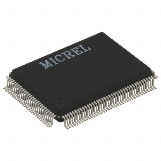
ICGOO电子元器件商城为您提供KSZ8993F由Micrel设计生产,在icgoo商城现货销售,并且可以通过原厂、代理商等渠道进行代购。 KSZ8993F价格参考¥询价-¥询价。MicrelKSZ8993F封装/规格:专用 IC, 10/100 Integrated Switch IC Port Switch/Network Interface 128-PQFP (14x20)。您可以下载KSZ8993F参考资料、Datasheet数据手册功能说明书,资料中有KSZ8993F 详细功能的应用电路图电压和使用方法及教程。
KSZ8993F是由Microchip Technology公司生产的一款专用IC,属于以太网交换芯片系列。该型号主要应用于工业和商业领域的网络通信设备中,提供高效的以太网数据交换功能。以下是其主要应用场景:

1. 小型网络交换机:KSZ8993F支持多达6个千兆以太网端口,适用于构建小型、低成本的网络交换机,满足家庭或小型办公室的网络需求。

2. 嵌入式系统:该芯片可集成到各种嵌入式系统中,例如工业控制设备、医疗设备或家用智能设备,提供可靠的以太网连接能力。

3. 物联网(IoT)网关:在物联网应用中,KSZ8993F可用于网关设备,实现多设备之间的高速数据传输与交换,支持智能家居、智慧城市等场景。

4. 安防监控系统:该芯片适合用于视频监控设备中的网络交换模块,确保高清视频流的稳定传输。

5. 汽车电子:尽管主要定位为商用和工业用途,KSZ8993F也可用于某些车载网络系统,提供车内设备之间的高速数据通信。

6. 打印机与存储设备:在网络打印机或NAS(网络附加存储)设备中,KSZ8993F能够提升数据传输效率,增强设备性能。

总结来说,KSZ8993F凭借其高性能、低功耗和灵活性,广泛应用于需要高效以太网数据交换的各类设备和系统中。
| 参数 | 数值 |
| 产品目录 | 集成电路 (IC)半导体 |
| 描述 | IC CONV MED 10/100 3PORT 128PQFP以太网 IC Single Chip Fast Ethernet Media Converter - Lead free |
| 产品分类 | |
| 品牌 | Micrel Inc |
| 产品手册 | |
| 产品图片 |
|
| rohs | 符合RoHS无铅 / 符合限制有害物质指令(RoHS)规范要求 |
| 产品系列 | 通信及网络 IC,以太网 IC,Micrel KSZ8993F- |
| 数据手册 | |
| 产品型号 | KSZ8993F |
| 产品 | Ethernet Switches |
| 产品目录页面 | |
| 产品种类 | 以太网 IC |
| 以太网连接类型 | 10/100 Base-TX |
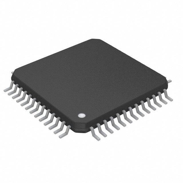
| 供应商器件封装 | 128-PQFP(14x20) |
| 其它名称 | 576-1033 |
| 包装 | 散装 |
| 商标 | Micrel |
| 安装类型 | 表面贴装 |
| 安装风格 | SMD/SMT |
| 封装 | Tray |
| 封装/外壳 | 128-BFQFP |
| 封装/箱体 | PQFP-128 |
| 工厂包装数量 | 66 |
| 应用 | 端口开关/网络接口 |
| 支持协议 | 802.3 |
| 收发器数量 | 2 Transceiver |
| 数据速率 | 100 Mbps |
| 最大工作温度 | + 70 C |
| 最大电源电流 | 160 mA |
| 最小工作温度 | 0 C |
| 标准包装 | 66 |
| 电源电压-最大 | 3.5 V |
| 电源电压-最小 | 3.1 V |
| 类型 | 10/100 集成开关 |
| 系列 | KSZ8993 |


- 商务部:美国ITC正式对集成电路等产品启动337调查
- 曝三星4nm工艺存在良率问题 高通将骁龙8 Gen1或转产台积电
- 太阳诱电将投资9.5亿元在常州建新厂生产MLCC 预计2023年完工
- 英特尔发布欧洲新工厂建设计划 深化IDM 2.0 战略
- 台积电先进制程称霸业界 有大客户加持明年业绩稳了
- 达到5530亿美元!SIA预计今年全球半导体销售额将创下新高
- 英特尔拟将自动驾驶子公司Mobileye上市 估值或超500亿美元
- 三星加码芯片和SET,合并消费电子和移动部门,撤换高东真等 CEO
- 三星电子宣布重大人事变动 还合并消费电子和移动部门
- 海关总署:前11个月进口集成电路产品价值2.52万亿元 增长14.8%


PDF Datasheet 数据手册内容提取
KS8993F/KS8993FL Single Chip Fast Ethernet Media Converter with TS-1000 OAM Revision 1.3 General Description The KS8993FL is the single supply version with all the identical rich features of the KS8993F. The Micrel KS8993F is the industry’s first single chip Fast Ethernet Media Converter with built-in OAM functions. The Features KS8993F integrates three MACs, two PHYs, OAM, frame buffer and high performance switch into a single chip. It is • First single-chip 10BASE-T/100BASE-TX to ideal for use in 100BASE-FX to 10BASE-T or 100BASE- 100BASE-FX media converter with TS-1000 OAM TX conversion in the FTTx market. • Integrated 3-Port 10/100 Ethernet Switch with 3 MACs and 2 PHYs The KS8993F provides remote loop back and OAM • Unique User Defined Register (UDR) feature brings (Operation, Administration and Maintenance) to manage OAM to low cost/complexity nodes subscriber access network from carrier center side to • Automatic MDI/MDI-X crossover with disable and terminal side. enable option • Non-blocking switch fabric assures fast packet The KS8993F supports advanced features such as rate delivery by utilizing an 1K MAC Address lookup table limiting, force flow control and link transparency. and a store-and-forward architecture The KS8993F with built-in Layer 2 switch capability will • Comprehensive LED indicator support for link, activity, filter packets and forward them to valid destination. It will full/half duplex and 10/100 speed discard any unwanted frames and frames with invalid • Full complement of MII/SNI, SPI, MIIM, SMI and I2C destination. interfaces • Low Power Dissipation:< 800mW (includes PHY transmit drivers) Block Diagram To Control Registers 1K look-up MDAI/uMtDoI-X T1P/T0H/X1Y/0F10X MOA 1M0A/1C0 01 Engine Queue F Management IF MDAI/uMtDoI-X T1P/0TH/X1Y/0F20X 1M0A/1C0 02 O, Flow IMntIIe r/ fSaNceI 1M0A/1C0 03 Control, VLA ManBaugfefemrent N T Frame SNI agging ,P Buffers InteSrPfaIce SPI riority CoMunIBters MIIM Interface Control SMI Registers EInEtPerRfaOcMe Interface I2C Bus P1 LED[3:0] LED Strap In Drivers Configuration Pins P2 LED[3:0] KS8993F / KS8993FL Micrel is a registered trademark of Micrel, Inc. Micrel Inc. • 2180 Fortune Drive • San Jose, CA 95131 • USA • tel +1 (408) 944-0800 • fax + 1 (408) 474-1000 • http://www.micrel.com June 2009 M9999-062509 hbwhelp@micrel.com or (408) 955-1690
Micrel, Inc. KS8993F/FL Features (continued) • Switch Management Features: • OAM Features: • Port mirroring/monitoring/sniffing: ingress and/or egress • Supports OAM sub-layer which conforms to TS-1000 traffic to any port or MII specification from TTC (Telecommunication Technology • MIB (Management Information Base) counters for fully Committee) compliant statistics gathering, 34 MIB counters per port • Sends and receives OAM frames to Center or Terminal • Full-chip hardware power-down (register configuration side not saved) • Loop back mode to support loop back packet from • Per-port based software power-save on PHY (idle link Center side to Terminal side detection, register configuration preserved) • Far-end fault detection with disable and enable • 0.18um CMOS technology • Link Transparency to indicate the link down from link • Voltages: partner Core 1.8V • Comprehensive Configuration Register access: I/O and Transceiver 3.3V • Serial Management Interface (SMI) to all internal • Available in 128-pin PQFP registers • MII Management (MIIM) Interface to PHY registers • SPI and I2C Interface to all internal registers • I/0 Pins Strapping and EEPROM to program selective Ordering Information registers in unmanaged switch mode • Control registers configurable on the fly (port-priority, Part Number Temperature Package 802.1p/d/q, AN…) Pb-Free Standard Range • QoS / CoS packets prioritization support • per-port, 802.1p and DiffServ based KSZ8993F KS8993F 0o– 70o C 128- • Re-mapping of 802.1p priority field per-port basis PQFP • Advanced Switch Features KSZ8993FL KS8993FL 0o– 70o C 128- • IEEE 802.1q VLAN support for up to 16 groups (full- PQFP range of VLAN ID) • VLAN ID tag/untag options, per-port basis • IEEE 802.1p/q tag insertion or removal on a per port basis (egress) • Programmable Rate Limiting from 0 to 100 Mbps at the ingress & egress port, rate options for high & low priority, per port basis • Broadcast storm protection with % control (global & per- port basis) • Double Tagging support June 2009 2 M9999-062509 hbwhelp@micrel.com or (408) 955-1690
Micrel, Inc. KS8993F/FL Revision History Revision Date Summary of Changes P0 1/14/03 Preliminary Information P1 2/11/03 Added separate Link and activity on port 1 and port 2’s LED (pin #20, pin #23, pin #25). Added disable auto MDI/MDIX (pin #28) Added select of MDI and MDIX (pin #29) P2 4/1/03 Updated register information P3 12/4/03 Started overhaul of datasheet. Updated strap option definition for pin #85. Renamed supply voltages and ground references to match schematics. Corrected Remote Loop back path. Updated MC registers descriptions. Changed 3.3V voltage pins to (3.3V or 2.5V). P4 3/11/04 Completed overhaul of datasheet. Revised datasheet format. Updated KS8993F block diagram. Updated Feature Highlights. Updated MC registers descriptions. Updated Electrical Characteristics (Vih, Vil, Voh, Vol). P5 3/23/04 Updated MC loop back description in pin #19 and register 11 bits[3:2], and path in loop back diagram. Updated flow diagram for Destination Address resolution flowchart, stage2. Changed S10 status bit from RO to R/W in register 81 bit[2]. Added KS8993FL to General Description (page 1) and Functional Description Overview (section 2.1). Updated pin description for pin 22 to the following: VDDC : For KS8993F, this is an input power pin for the 1.8V digital core VDD. VOUT_1V8 : For KS8993FL, this is an 1.8V output power pin to supply the KS8993FL’s input power pins: VDDAP (pin 63), VDDC (pins 91, 123) and VDDA (pins 38, 43, 57). Improved/clarified pin description. 1.0 8/26/04 Updated PPM spec for 25 MHz crystal/oscillator. Improved/clarified pin description for P1LCRCD (pin 18), P2MDIX (pin 29) and MDIO (pin 95). Corrected aging time. Removed loop back support from MIIM and Port Control Registers, so that there is no confusion with MC loop back which is used exclusively in KS8993F application. Updated HWPOVR description in section 2.2.5. Corrected default definition for FEF in section 2.3.6, and MIIM and Port Control Registers. Added register note to indicate port sniffing is not supported if the unicast packets can cross VLAN boundary bit is set. Improved/clarified switch/PHY registers descriptions for Force MDIX and CRC drop. Improved/clarified MC registers descriptions for Remote Command (registers 74, 75, 76), My Status (registers 80, 81) and LNK Partner Status (registers 88, 89). Added register note to set Register 85: My Model Info (1) to values of 0x22, 0x26, 0x2A and 0x2E if the Remote Command feature is used. Updated MIB counters descriptions to indicate counter overflow must be tracked by application. 1.1 4/7/05 Corrected VDDIO, VDDATX, VDDARX supply pins to 3.3V only. Updated reset timing requirement. Corrected 10BASE-T Transmitter Jitters Added. 1.2 5/22/06 Removed Industrial Temperature line from Features and Ordering info. 1.3 6/25/09 Add the parts KSZ8993F, KSZ8993FL on the order information June 2009 3 M9999-062509 hbwhelp@micrel.com or (408) 955-1690
Micrel, Inc. KS8993F/FL Table Of Contents 1 Signal Description.........................................................................................................................9 1.1 KS8993F Pin Diagram...........................................................................................................................................................9 1.2 Pin Description and I/O Assignment....................................................................................................................................10 2 Functional Description................................................................................................................20 2.1 Overview..............................................................................................................................................................................20 2.2 Media Converter Function....................................................................................................................................................20 2.2.1 OAM (Operations, Administration, and Management) Frame Format.....................................................................20 2.2.2 MC (Media Converter) Mode...................................................................................................................................22 2.2.3 MC Loop Back Function..........................................................................................................................................22 2.2.4 Registers for Media Converter Functions................................................................................................................23 2.2.5 Unique I/O Feature Definition..................................................................................................................................23 2.2.6 Port 1 LED Indicator Definition................................................................................................................................24 2.2.7 Port 2 LED Indicator Definition................................................................................................................................24 2.3 Physical Transceiver............................................................................................................................................................25 2.3.1 100BASE-TX Transmit............................................................................................................................................25 2.3.2 100BASE-TX Receive.............................................................................................................................................25 2.3.3 PLL Clock Synthesizer............................................................................................................................................25 2.3.4 Scrambler/De-scrambler (100BASE-TX only).........................................................................................................25 2.3.5 100BASE-FX Operation and Signal Detection........................................................................................................25 2.3.6 100BASE-FX Far-End Fault (FEF)..........................................................................................................................26 2.3.7 10BASE-T Transmit and Receive............................................................................................................................26 2.3.8 Power Management.................................................................................................................................................27 2.3.9 Auto MDI/MDI-X Crossover.....................................................................................................................................27 2.3.10 Auto Negotiation......................................................................................................................................................29 2.4 MAC and Switch Function....................................................................................................................................................29 2.4.1 Address Look Up.....................................................................................................................................................29 2.4.2 Learning...................................................................................................................................................................30 2.4.3 Migration..................................................................................................................................................................30 2.4.4 Aging.......................................................................................................................................................................30 2.4.5 Forwarding...............................................................................................................................................................30 2.4.6 Switching Engine.....................................................................................................................................................33 2.4.7 MAC operation.........................................................................................................................................................33 2.4.8 Back-off Algorithm...................................................................................................................................................33 2.4.9 Late Collision...........................................................................................................................................................33 2.4.10 Illegal Frames..........................................................................................................................................................33 2.4.11 Flow Control............................................................................................................................................................33 2.4.12 Half Duplex Back Pressure......................................................................................................................................34 2.4.13 Broadcast Storm Protection.....................................................................................................................................34 2.5 MII Interface Operation........................................................................................................................................................34 2.6 SNI (7-wire) Interface Operation..........................................................................................................................................35 2.7 MII Management Interface (MIIM)........................................................................................................................................36 2.8 Serial Management Interface (SMI).....................................................................................................................................36 2.9 Advanced Switch Function...................................................................................................................................................37 2.9.1 Port Mirroring Support.............................................................................................................................................37 2.9.2 IEEE 802.1Q VLAN support....................................................................................................................................38 2.9.3 QoS Priority.............................................................................................................................................................39 2.9.4 Rate Limit Support...................................................................................................................................................41 2.10 Configuration Interface.........................................................................................................................................................41 2.10.1 I2C Master Serial Bus Configuration........................................................................................................................42 2.10.2 I2C Slave Serial Bus Configuration..........................................................................................................................43 2.10.3 SPI Slave Serial Bus Configuration.........................................................................................................................43 3 MII Management (MIIM) Registers.............................................................................................47 Register 0: MII Basic Control..............................................................................................................................................47 Register 1: MII Basic Status................................................................................................................................................48 Register 2: PHYID HIGH.....................................................................................................................................................48 Register 3: PHYID LOW......................................................................................................................................................48 Register 4: Auto-Negotiation Advertisement Ability............................................................................................................49 June 2009 4 M9999-062509 hbwhelp@micrel.com or (408) 955-1690
Micrel, Inc. KS8993F/FL Register 5: Auto-Negotiation Link Partner Ability................................................................................................................49 4 Register Map: Switch, MC, & PHY (8 bits registers)..................................................................50 4.1 Global Registers...................................................................................................................................................................51 Register 0 (0x00): Chip ID0.................................................................................................................................................51 Register 1 (0x01): Chip ID1 / Start Switch...........................................................................................................................51 Register 2 (0x02): Global Control 0.....................................................................................................................................51 Register 3 (0x03): Global Control 1.....................................................................................................................................52 Register 4 (0x04): Global Control 2.....................................................................................................................................53 Register 5 (0x05): Global Control 3.....................................................................................................................................53 Register 6 (0x06): Global Control 4.....................................................................................................................................54 Register 7 (0x07): Global Control 5.....................................................................................................................................55 Register 8 (0x08): Global Control 6.....................................................................................................................................55 Register 9 (0x09): Global Control 7.....................................................................................................................................55 Register 10 (0x0A): Global Control 8..................................................................................................................................55 Register 11 (0x0B): Global Control 9..................................................................................................................................55 Register 12 (0x0C): Reserved Register..............................................................................................................................56 Register 13 (0x0D): User Defined Register 1......................................................................................................................56 Register 14 (0x0E): User Defined Register 2......................................................................................................................57 Register 15 (0x0F): User Defined Register 3......................................................................................................................57 4.2 Port Registers......................................................................................................................................................................57 Register 16 (0x10): Port 1 Control 0...................................................................................................................................57 Register 17 (0x11): Port 1 Control 1...................................................................................................................................58 Register 18 (0x12): Port 1 Control 2...................................................................................................................................58 Register 19 (0x13): Port 1 Control 3...................................................................................................................................59 Register 20 (0x14): Port 1 Control 4...................................................................................................................................59 Register 21 (0x15): Port 1 Control 5...................................................................................................................................60 Register 22 (0x16): Port 1 Control 6...................................................................................................................................60 Register 23 (0x17): Port 1 Control 7...................................................................................................................................60 Register 24 (0x18): Port 1 Control 8...................................................................................................................................60 Register 25 (0x19): Port 1 Control 9...................................................................................................................................60 Register 26 (0x1A): Port 1 Control 10.................................................................................................................................60 Register 27 (0x1B): Port 1 Control 11.................................................................................................................................61 Register 28 (0x1C): Port 1 Control 12.................................................................................................................................61 Register 29 (0x1D): Port 1 Control 13.................................................................................................................................62 Register 30 (0x1E): Port 1 Status 0....................................................................................................................................63 Register 31 (0x1F): Port 1 Status 1.....................................................................................................................................64 4.3 Media Converter Registers..................................................................................................................................................65 Register 64 (0x40): PHY Address.......................................................................................................................................65 Register 65 (0x41): Center Side Status..............................................................................................................................65 Register 66 (0x42): Center Side Command........................................................................................................................66 Register 67 (0x43): PHY-SW Initialize................................................................................................................................66 Register 68 (0x44): Loop Back Setup1...............................................................................................................................68 Register 69 (0x45): Loop Back Setup2...............................................................................................................................68 Register 70 (0x46): Loop Back Result Counter for CRC Error............................................................................................69 Register 71 (0x47): Loop Back Result Counter for Timeout................................................................................................69 Register 72 (0x48): Loop Back Result Counter for Good Packet........................................................................................69 Register 73 (0x49): Additional Status (Center and Terminal side)......................................................................................69 Register 74 (0x4A): Remote Command 1...........................................................................................................................70 Register 75 (0x4B): Remote Command 2...........................................................................................................................70 Register 76 (0x4C): Remote Command 3...........................................................................................................................71 Register 77 (0x4D): Valid MC Packet Transmitted Counter................................................................................................71 Register 78 (0x4E): Valid MC Packet Received Counter....................................................................................................71 Register 79 (0x4F): Shadow of 0x58h Register..................................................................................................................71 Register 80 (0x50): My Status 1 (Terminal and Center side)..............................................................................................72 Register 81 (0x51): My Status 2..........................................................................................................................................72 Register 82 (0x52): My Vendor Info (1)...............................................................................................................................73 Register 83 (0x53): My Vendor Info (2)...............................................................................................................................73 Register 84 (0x54): My Vendor Info (3)...............................................................................................................................73 Register 85 (0x55): My Model Info (1).................................................................................................................................73 Register 86 (0x56): My Model Info (2).................................................................................................................................73 Register 87 (0x57): My Model Info (3).................................................................................................................................73 June 2009 5 M9999-062509 hbwhelp@micrel.com or (408) 955-1690
Micrel, Inc. KS8993F/FL Register 88 (0x58): LNK Partner Status (1)........................................................................................................................74 Register 89 (0x59): LNK Partner Status (2)........................................................................................................................74 Register 90 (0x5A): LNK Partner Vendor Info (1)...............................................................................................................74 Register 91 (0x5B): LNK Partner Vendor Info (2)................................................................................................................74 Register 92 (0x5C): LNK Partner Vendor Info (3)...............................................................................................................74 Register 93 (0x5D): LNK Partner Model Info (1).................................................................................................................74 Register 94 (0x5E): LNK Partner Model Info (2).................................................................................................................74 Register 95 (0x5F): LNK Partner Model Info (3)..................................................................................................................74 4.4 Advanced Control Registers................................................................................................................................................75 Register 96 (0x60): TOS Priority Control Register 0...........................................................................................................75 Register 97 (0x61): TOS Priority Control Register 1...........................................................................................................75 Register 98 (0x62): TOS Priority Control Register 2...........................................................................................................75 Register 99 (0x63): TOS Priority Control Register 3...........................................................................................................75 Register 100 (0x64): TOS Priority Control Register 4.........................................................................................................75 Register 101 (0x65): TOS Priority Control Register 5.........................................................................................................75 Register 102 (0x66): TOS Priority Control Register 6.........................................................................................................75 Register 103 (0x67): TOS Priority Control Register 7.........................................................................................................75 Register 104 (0x68): MAC Address Register 0...................................................................................................................76 Register 105 (0x69): MAC Address Register 1...................................................................................................................76 Register 106 (0x6A): MAC Address Register 2...................................................................................................................76 Register 107 (0x6B): MAC Address Register 3...................................................................................................................76 Register 108 (0x6C): MAC Address Register 4...................................................................................................................76 Register 109 (0x6D): MAC Address Register 5...................................................................................................................76 Register 110 (0x6E): Indirect Access Control 0..................................................................................................................76 Register 111 (0x6F): Indirect Access Control 1..................................................................................................................76 Register 112 (0x70): Indirect Data Register 8.....................................................................................................................77 Register 113 (0x71): Indirect Data Register 7.....................................................................................................................77 Register 114 (0x72): Indirect Data Register 6.....................................................................................................................77 Register 115 (0x73): Indirect Data Register 5.....................................................................................................................77 Register 116 (0x74): Indirect Data Register 4.....................................................................................................................77 Register 117 (0x75): Indirect Data Register 3.....................................................................................................................77 Register 118 (0x76): Indirect Data Register 2.....................................................................................................................77 Register 119 (0x77): Indirect Data Register 1.....................................................................................................................77 Register 120 (0x78): Indirect Data Register 0.....................................................................................................................77 Register 121 (0x79): Digital Testing Status 0......................................................................................................................77 Register 122 (0x7A): Digital Testing Status 1.....................................................................................................................77 Register 123 (0x7B): Digital Testing Control 0....................................................................................................................78 Register 124 (0x7C): Digital Testing Control 1....................................................................................................................78 Register 125 (0x7D): Analog Testing Control 0...................................................................................................................78 Register 126 (0x7E): Analog Testing Control 1..................................................................................................................78 Register 127 (0x7F): Analog Testing Status.......................................................................................................................78 4.5 Static MAC Address Table...................................................................................................................................................78 4.6 VLAN Table..........................................................................................................................................................................79 4.7 Dynamic MAC Address Table..............................................................................................................................................80 4.8 MIB (Management Information Base) Counters...................................................................................................................81 5 Electrical Specifications..............................................................................................................86 5.1 Absolute Maximum Ratings.................................................................................................................................................86 5.2 Recommended Operating Conditions..................................................................................................................................86 5.3 Electrical Characteristics......................................................................................................................................................87 5.4 100BASE-FX Electrical Specification...................................................................................................................................88 6 Timing Specifications..................................................................................................................89 6.1 EEPROM Timing..................................................................................................................................................................89 6.2 SNI Timing...........................................................................................................................................................................90 6.3 MII Timing............................................................................................................................................................................91 6.3.1 MAC Mode MII Timing.............................................................................................................................................91 6.3.2 PHY Mode MII Timing..............................................................................................................................................92 6.3.3 SPI Timing...............................................................................................................................................................92 6.3.4 MDC/MDIO Timing...................................................................................................................................................95 6.3.5 Auto Negotiation Timing..........................................................................................................................................96 6.4 Reset Timing........................................................................................................................................................................97 6.5 Reset Circuit.........................................................................................................................................................................98 June 2009 6 M9999-062509 hbwhelp@micrel.com or (408) 955-1690
Micrel, Inc. KS8993F/FL 7 Selection of Isolation Transformer..............................................................................................99 8 Selection of Crystal/Oscillator.....................................................................................................99 9 Package Information.................................................................................................................100 June 2009 7 M9999-062509 hbwhelp@micrel.com or (408) 955-1690
Micrel, Inc. KS8993F/FL List of Tables Table 1: FX and TX Mode Selection..................................................................................................................................................26 Table 2: MDI/MDI-X Pin Definition.....................................................................................................................................................27 Table 3: MII Signals...........................................................................................................................................................................35 Table 4: SNI (7-wire) Signals.............................................................................................................................................................35 Table 5: MII Management Interface frame format.............................................................................................................................36 Table 6: Serial Management Interface (SMI) frame format...............................................................................................................37 Table 7: FID+DA look up in VLAN mode...........................................................................................................................................39 Table 8: FID+SA look up in VLAN mode...........................................................................................................................................39 Table 9: KS8993F SPI Connections..................................................................................................................................................44 Table 10: Format of Static MAC Table (8 entries).............................................................................................................................79 Table 11: Format of Static VLAN Table (16 entries)..........................................................................................................................80 Table 12: Format of Dynamic MAC Table (1K entries)......................................................................................................................81 Table 13: Format of “Per Port” MIB Counters....................................................................................................................................82 Table 14: Port 1’s “Per Port” MIB Counters Indirect Memory Offsets................................................................................................82 Table 15: Format of “All Port Dropped Packet” MIB Counters..........................................................................................................84 Table 16: “All Port Dropped Packet” MIB Counters Indirect Memory Offsets....................................................................................84 Table 17: EEPROM Timing Parameters............................................................................................................................................89 Table 18: SNI Timing Parameters.....................................................................................................................................................90 Table 19: MAC mode MII Timing Parameters...................................................................................................................................91 Table 20: PHY Mode MII Timing Parameters....................................................................................................................................92 Table 21: SPI Input Timing Parameters............................................................................................................................................93 Table 22: SPI Output Timing Parameters..........................................................................................................................................94 Table 23: Reset Timing Parameters..................................................................................................................................................97 Table 24: Transformer Selection Criteria...........................................................................................................................................99 Table 25: Qualified Single Port Magnetic..........................................................................................................................................99 Table 26: Crystal/Oscillator Selection Criteria...................................................................................................................................99 List of Figures Figure 1: Typical Straight Cable Connection.....................................................................................................................................28 Figure 2: Typical Crossover Cable Connection.................................................................................................................................28 Figure 3: Auto Negotiation and Parallel Detection............................................................................................................................29 Figure 4: Destination Address look up flowchart, stage 1.................................................................................................................31 Figure 5: Destination Address resolution flowchart, stage 2.............................................................................................................32 Figure 6: 802.1p Priority Field Format...............................................................................................................................................40 Figure 7: KS8993F EEPROM Configuration Timing Diagram...........................................................................................................42 Figure 8: SPI Write Data Cycle.........................................................................................................................................................45 Figure 9: SPI Read Data Cycle.........................................................................................................................................................45 Figure 10: SPI Multiple Write.............................................................................................................................................................46 Figure 11: SPI Multiple Read.............................................................................................................................................................46 Figure 12: EEPROM Interface Input Timing Diagram.......................................................................................................................89 Figure 13: EEPROM Interface Output Timing Diagram.....................................................................................................................89 Figure 14: SNI Input Timing Diagram................................................................................................................................................90 Figure 15: SNI Output Timing Diagram.............................................................................................................................................90 Figure 16: MAC Mode MII Timing - Data received from MII..............................................................................................................91 Figure 17: MAC Mode MII Timing - Data transmitted to MII..............................................................................................................91 Figure 18: PHY Mode MII Timing – Data received from MII..............................................................................................................92 Figure 19: PHY Mode MII Timing - Data transmitted to MII...............................................................................................................92 Figure 20: SPI Input Timing...............................................................................................................................................................93 Figure 21: SPI Output Timing............................................................................................................................................................94 Figure 22: MDC/MDIO Timing for MIIM and SMI Interfaces..............................................................................................................95 Figure 23: Auto Negotiation Timing...................................................................................................................................................96 Figure 24: Reset Timing....................................................................................................................................................................97 Figure 25: Recommended Reset Circuit...........................................................................................................................................98 Figure 26: Recommended Reset Circuit for interfacing with CPU/FPGA Reset Output....................................................................98 Figure 27: 128-pin PQFP Package Outline Drawing.......................................................................................................................100 June 2009 8 M9999-062509 hbwhelp@micrel.com or (408) 955-1690
Micrel, Inc. KS8993F/FL 1 Signal Description 1.1 KS8993F Pin Diagram PV31PS0PS1SPIS_NSDASCLSPIQMDIOMDCPRSEL0PRSEL1VDDCDGNDSCONF0SCONF1SCRSSCOLSMRXD0SMRXD1SMRXD2SMRXD3SMRXDVSMRXCVDDIODGNDSMTXCSMTXERSMTXD0SMTXD1SMTXD2SMTXD3SMTXENLEDSEL0SMACBPENRST_NX2X1 PV32 103102101100999897969594939291908988878685848382818079787776757473727170696867666564 AGND PV21 104 63 VDDAP PV23 105 62 AGND DGND 106 61 ISET VDDIO 107 60 TEST2 PV12 108 59 TEST1 PV13 109 58 AGND P3_1PEN 110 57 VDDA P2_1PEN 111 56 TXP2 P1_1PEN 112 55 TXM2 P3_TXQ2 113 54 AGND P2_TXQ2 114 KS8993F 53 RXP2 P1_TXQ2 115 52 RXM2 P3_PP 116 51 VDDARX P2_PP 117 50 VDDATX P1_PP 118 49 TXM1 P3_TAGINS 119 48 TXP1 P2_TAGINS 120 47 AGND P1_TAGINS 121 46 RXM1 DGND 122 45 RXP1 VDDC 123 44 FXSD1 P3_TAGRM 124 43 VDDA P2_TAGRM 125 42 AGND P1_TAGRM 126 41 MUX2 TESTEN 127 40 MUX1 SCANEN 128 39 AGND 1234567891011121314151617181920212223242526272829303132333435363738 P1LED2P1LED1P1LED0P2LED2P2LED1P2LED0DGNDVDDIOMCHSMCCSPDD#ADVFCP2ANENP2SPDP2DPXP2FFCP1FSTP1CRCDP1LPBMP2LED3DGNDVDDCLEDSEL1NCP1LED3NCHWPOVR2MDIXDISP2MDIXP1ANENP1SPDP1PDXP1FFCML_ENDIAGFPWRDNAGNDVDDA P June 2009 9 M9999-062509 hbwhelp@micrel.com or (408) 955-1690
Micrel, Inc. KS8993F/FL 1.2 Pin Description and I/O Assignment Pin # Pin Name Type Description 1 P1LED2 I(pu)/O Port 1 LED indicators, defined as below: 2 P1LED1 I(pu)/O 3 P1LED0 I(pu)/O [LEDSEL1, LEDSEL0] [0,0] [0,1] P1LED3 ------ ------ P1LED2 LINK/ACT 100LINK/ACT P1LED1 FULLD/COL 10LINK/ACT P1LED0 SPEED FULL_DPX [LEDSEL1, LEDSEL0] [1,0] [1,1] P1LED3 ACT ------ P1LED2 LINK ------ P1LED1 FULL_DPX/COL ------ P1LED0 SPEED ------ Notes: LEDSEL0 is external strap-in pin #70. LEDSEL1 is external strap-in pin #23. P1LED3 is pin #25. During reset, P1LED[2:0] are inputs for internal testing. 4 P2LED2 I(pu)/O Port 2 LED indicators, defined as below: 5 P2LED1 I(pu)/O 6 P2LED0 I(pu)/O [LEDSEL1, LEDSEL0] [0,0] [0,1] P2LED3 ------ ------ P2LED2 LINK/ACT 100LINK/ACT P2LED1 FULLD/COL 10LINK/ACT P2LED0 SPEED FULL_DPX [LEDSEL1, LEDSEL0] [1,0] [1,1] P2LED3 ACT ------ P2LED2 LINK ------ P2LED1 FULL_DPX/COL ------ P2LED0 SPEED ------ Notes: LEDSEL0 is external strap-in pin #70. LEDSEL1 is external strap-in pin #23. P2LED3 is pin #20. During reset, P2LED[2:0] are inputs for internal testing. 7 DGND Gnd Digital ground 8 VDDIO Pwr 3.3V digital VDD June 2009 10 M9999-062509 hbwhelp@micrel.com or (408) 955-1690
Micrel, Inc. KS8993F/FL Pin # Pin Name Type Description 9 MCHS Ipd KS8993F operating modes, defined as below: 10 MCCS Ipd (MCHS, MCCS) Description Normal 3 port switch mode (3 MAC + 2 PHY) MC mode is disabled. Port 1 is either Fiber or UTP. (0, 0) Port 2 is UTP. Port 3 (MII) is enabled. Center MC mode (3 MAC + 2 PHY) MC mode is enabled. Port 1 is Fiber and has Center MC enabled. (0, 1) Port 2 is UTP. Port 3 (MII) is enabled. Terminal MC mode (2 MAC + 2 PHY) MC mode is enabled. Port 1 is Fiber and has Terminal MC enabled. (1, 0) Port 2 is UTP. Port 3 (MII) is disabled. Terminal MC mode (3 MAC + 2 PHY) MC mode is enabled. Port 1 is Fiber and has Terminal MC enabled. (1, 1) Port 2 is UTP. Port 3 (MII) is enabled. 11 PDD# Ipu Power Down Detect 1 = normal operation 0 = power down detected In Terminal MC mode (pin MCHS is ‘1’), a high to low transition to this pin will cause port 1 (fiber) to generate and send out an “Indicate Terminal MC Condition” OAM frame with the S0 status bit set to ‘1’. 12 ADVFC Ipu 1= advertise the switch’s flow control capability via auto negotiation. 0 = will not advertise the switch’s flow control capability via auto negotiation. 13 P2ANEN Ipu 1 = enable auto negotiation on port 2. 0 = disable auto negotiation on port 2. 14 P2SPD Ipd 1 = Force port 2 to 100BT if P2ANEN = 0. 0 = Force port 2 to 10BT if P2ANEN = 0. 15 P2DPX Ipd 1 = port 2 default to full duplex mode if P2ANEN = 1 and auto negotiation fails. Force port 2 in full duplex mode if P2ANEN = 0. 0 = port 2 default to half duplex mode if P2ANEN = 1 and auto negotiation fails. Force port 2 in half duplex mode if P2ANEN = 0. 16 P2FFC Ipd 1 = always enable (force) port 2 flow control feature. 0 = port 2 flow control feature enable is determined by auto negotiation result. 17 P1FST Opu 1 = normal function 0 = MC in loop back mode, or MC abnormal conditions happen 18 P1LCRCD Ipd In MC loop back mode, 1 = Drop OAM frames and Ethernet frames with the following errors – June 2009 11 M9999-062509 hbwhelp@micrel.com or (408) 955-1690
Micrel, Inc. KS8993F/FL Pin # Pin Name Type Description CRC, undersize, oversize. Loop back Ethernet frames with only good CRC and valid length. 0 = Drop OAM frames only. Loop back all Ethernet frames including those with errors. 19 P1LPBM Ipd 0 = perform MC loop back at MAC of port 2 1 = reserve. Do not use. 20 P2LED3 Opd Port 2 LED Indicator Note: Internal pull down is weak; it will not turn ON the LED. See description in pin# (4). 21 DGND Gnd Digital ground 22 VDDC / VOUT_1V8 Pwr VDDC : For KS8993F, this is an input power pin for the 1.8V digital core VDD. VOUT_1V8 : For KS8993FL, this is an 1.8V output power pin to supply the KS8993FL’s input power pins: VDDAP (pin 63), VDDC (pins 91, 123) and VDDA (pins 38, 43, 57). 23 LEDSEL1 I LED display mode select pd See description in pin# (1,4). 24 NC O Reserved pd 25 P1LED3 O Port 1 LED Indicator pd Note: An external 1K pull down is needed on this pin if it is connected to a LED. See description in pin# (1). 26 NC O Reserved pd 27 HWPOVR Ipd Hardware Pin Overwrite 0 = Disable. All strap-in pins configurations are overwritten by the EEPROM configuration data. 1 = Enable. All strap-in pins configurations are overwritten by the EEPROM configuration data, except for P2ANEN (pin 13), P2SPD (pin 14), P2DPX (pin 15) and ML_EN (pin 34). 28 P2MDIXDIS Ipd Port 2 auto MDI/MDI-X 0 = enable (default) 1 = disable 29 P2MDIX Ipd Port 2 MDI/MDI-X setting when auto MDI/MDI-X is disabled 0 = MDI-X (default), {transmit on TXP2/TXM2 pins} 1 = MDI, {transmit on RXP2/RXM2 pins} 30 P1ANEN Ipu 1 = enable auto negotiation on port 1 0 = disable auto negotiation on port 1 31 P1SPD Ipd 1 = Force port 1 to 100BT if P1ANEN = 0. 0 = Force port 1 to 10BT if P1ANEN = 0. 32 P1DPX Ipd 1 = port 1 default to full duplex mode if P1ANEN = 1 and auto negotiation fails. Force port 1 in full duplex mode if P1ANEN = 0. 0 = port 1 default to half duplex mode if P1ANEN = 1 and auto negotiation fails. Force port 1 in half duplex mode if P1ANEN = 0. 33 P1FFC Ipd 1 = always enable (force) port 1 flow control feature 0 = port 1 flow control feature enable is determined by auto negotiation result. 34 ML_EN Ipd 1 = enable missing link June 2009 12 M9999-062509 hbwhelp@micrel.com or (408) 955-1690
Micrel, Inc. KS8993F/FL Pin # Pin Name Type Description 0 = disable missing link 35 DIAGF Ipd 1 = diagnostic fail 0 = diagnostic normal 36 PWRDN I Chip power down input (active low) 37 AGND Gnd Analog ground 38 VDDA Pwr 1.8V analog VDD 39 AGND Gnd Analog ground 40 MUX1 I Factory test pin – float for normal operation 41 MUX2 I Factory test pin – float for normal operation 42 AGND Gnd Analog ground 43 VDDA Pwr 1.8V analog VDD 44 FXSD1 I Fiber signal detect / factory test pin 45 RXP1 I/O Physical receive or transmit signal (+ differential) 46 RXM1 I/O Physical receive or transmit signal (- differential) 47 AGND Gnd Analog ground 48 TXP1 I/O Physical transmit or receive signal (+ differential) 49 TXM1 I/O Physical transmit or receive signal (- differential) 50 VDDATX Pwr 3.3V analog VDD 51 VDDARX Pwr 3.3V analog VDD 52 RXM2 I/O Physical receive or transmit signal (– differential) 53 RXP2 I/O Physical receive or transmit signal (+ differential) 54 AGND Gnd Analog ground 55 TXM2 I/O Physical transmit or receive signal (– differential) 56 TXP2 I/O Physical transmit or receive signal (+ differential) 57 VDDA Pwr 1.8V analog VDD 58 AGND Gnd Analog ground 59 TEST1 I Factory test pin – float for normal operation 60 TEST2 I Factory test pin – float for normal operation 61 ISET O Set physical transmit output current. Pull down this pin with a 3.01K 1% resistor to ground. 62 AGND Gnd Analog ground 63 VDDAP Pwr 1.8V analog VDD for PLL 64 AGND Gnd Analog ground 65 X1 I 25 MHz crystal/oscillator clock connections 66 X2 O Pins (X1, X2) connect to a crystal. If an oscillator is used, X1 connects to a 3.3V tolerant oscillator and X2 is a no connect. Note: Clock is +/- 50ppm for both crystal and oscillator. 67 RST_N Ipu Hardware reset pin (active low) 68 BPEN Ipd Half Duplex Backpressure 1 = enable 0 = disable 69 SMAC Ipd Special Mac Mode In this mode, the switch will do faster backoffs than normal. 1 = enable 0 = disable 70 LEDSEL0 Ipd LED display mode select See description in pin# (1,4). 71 SMTXEN Ipd Switch MII transmit enable 72 SMTXD3 Ipd Switch MII transmit data bit 3 June 2009 13 M9999-062509 hbwhelp@micrel.com or (408) 955-1690
Micrel, Inc. KS8993F/FL Pin # Pin Name Type Description 73 SMTXD2 Ipd Switch MII transmit data bit 2 74 SMTXD1 Ipd Switch MII transmit data bit 1 75 SMTXD0 Ipd Switch MII transmit data bit 0 76 SMTXER Ipd Switch MII transmit error 77 SMTXC Ipd/O Switch MII transmit clock Output in PHY MII mode Input in MAC MII mode 78 DGND Gnd Digital ground 79 VDDIO Pwr 3.3V digital VDD 80 SMRXC Ipd/O Switch MII receive clock Output in PHY MII mode Input in MAC MII mode 81 SMRXDV O Switch MII receive data valid 82 SMRXD3 Ipd/O Switch MII receive data bit 3 Strap option: Switch MII full duplex flow control PD (default) = disable PU = enable 83 SMRXD2 Ipd / O Switch MII receive bit 2 Strap option: Switch MII is in PD (default) = full duplex mode PU = half duplex mode 84 SMRXD1 Ipd/O Switch MII receive bit 1 Strap option: Switch MII is in PD (default) = 100Mbps mode PU = 10Mbps mode 85 SMRXD0 Ipd/O Switch MII receive bit 0 Strap option: Switch will accept packet size up to PD (default) = 1536 bytes (inclusive); PU = 1522 bytes (tagged), 1518 bytes (untagged) 86 SCOL Ipd/O Switch MII collision detect 87 SCRS Ipd/O Switch MII carrier sense 88 SCONF1 Ipd Switch MII interface configuration 89 SCONF0 Ipd (SCONF1, SCONF0) Description (0,0) disable, output tri-stated (0,1) PHY mode MII (1,0) MAC mode MII (1,1) PHY mode SNI 90 DGND Gnd Digital ground 91 VDDC Pwr 1.8V digital VDD 92 PRSEL1 Ipd Priority Select Select queue servicing if using split queues. Use the table June 2009 14 M9999-062509 hbwhelp@micrel.com or (408) 955-1690
Micrel, Inc. KS8993F/FL Pin # Pin Name Type Description 93 PRSEL0 Ipd below to select the desired servicing. Note that this selection affects all split transmit queue ports in the same way. (PRSEL,PRSEL0) Description (0,0) Transmit all high priority before low priority (0,1) Transmit high priority and low priority at 10:1 ratio. (1,0) Transmit high priority and low priority at 5:1 ratio. (1,1) Transmit high priority and low priority at 2:1 ratio. 94 MDC Ipu MII Management interface: clock input 95 MDIO Ipu/O MII Management interface: data input/output Note: An external 4.7K pull up is needed on this pin when it is in use. 96 SPIQ Opu SPI slave mode: serial data output See description in pin# (100, 101) 97 SCL Ipu/O SPI slave mode / I2C slave mode: clock input I2C master mode: clock output See description in pin# (100, 101) 98 SDA Ipu/O SPI slave mode: serial data input I2C master/slave mode: serial data input/output See description in pin# (100, 101) 99 SPIS_N Ipu SPI slave mode: chip select (active low) When SPIS_N is high, the KS8993F is deselected and SPIQ is held in high impedance state. A high-to-low transition is used to initiate SPI data transfer. See description in pin# (100, 101) 100 PS1 Ipd Serial bus configuration pins to select mode of access to KS8993F internal June 2009 15 M9999-062509 hbwhelp@micrel.com or (408) 955-1690
Micrel, Inc. KS8993F/FL Pin # Pin Name Type Description 101 PS0 Ipd registers. [PS1, PS0] = [0, 0] --- I2C master (EEPROM) mode (If EEPROM is not detected, the power up default values of the KS8993F internal registers will be used) Interface Signals Type Description SPIQ O Not used. (tri-stated) SCL O I2C clock SDA I/O I2C data I/O SPIS_N Ipu Not used. [PS1, PS0] = [0, 1] --- I2C slave mode The external I2C master will drive the SCL clock. The KS8993F device addresses are: 1011_1111 <read> 1011_1110 <write> Interface Signals Type Description SPIQ O Not used. (tri-stated) SCL I I2C clock SDA I/O I2C data I/O SPIS_N Ipu Not used. [PS1, PS0] = [1, 0] --- SPI slave mode Interface Signals Type Description SPIQ O SPI Data Out SCL I SPI clock SDA I SPI Data In SPIS_N Ipu SPI chip select [PS1, PS0] = [1, 1] --- SMI mode In this mode, the KS8993F provides access to all its internal 8 bit registers thru its MDC and MDIO pins. Note When (PS1, PS0) ≠ (1,1), the KS8993F provides access to its 16 bit MIIM registers thru its MDC and MDIO pins. 102 PV31 Ipu Port 3 port based VLAN mask bits. Use to select which ports may 103 PV32 Ipu transmit packets received on port 3. PV31 = 1, port 1 may transmit packets received on port 3. PV31 = 0, port 1 will not transmit any packets received on port 3. PV32 = 1, port 2 may transmit packets received on port 3. PV32 = 0, port 2 will not transmit any packets received on port 3. 104 PV21 Ipu Port 2 port based VLAN mask bits. Use to select which ports may 105 PV23 Ipu transmit packets received on port 2. PV21 = 1, port 1 may transmit packets received on port 2. PV21 = 0, port 1 will not transmit any packets received on port 2. PV23 = 1, port 3 may transmit packets received on port 2. PV23 = 0, port 3 will not transmit any packets received on port 2. 106 DGND Gnd Digital ground June 2009 16 M9999-062509 hbwhelp@micrel.com or (408) 955-1690
Micrel, Inc. KS8993F/FL Pin # Pin Name Type Description 107 VDDIO Pwr 3.3V digital VDD 108 PV12 Ipu Port 1 port based VLAN mask bits. Use to select which ports may 109 PV13 Ipu transmit packets received on port 1. PV12 = 1, port 2 may transmit packets received on port 1. PV12 = 0, port 2 will not transmit any packets received on port 1. PV13 = 1, port 3 may transmit packets received on port 1. PV13 = 0, port 3 will not transmit any packets received on port 1. 110 P3_1PEN Ipd Enable 802.1p priority classification on port 3 ingress 1 = enable 0 = disable Enable is from the receive perspective. If 802.1p processing is disabled or there is no tag, priority is determined by the P3_PP pin. 111 P2_1PEN Ipd Enable 802.1p priority classification on port 2 ingress 1 = enable 0 = disable Enable is from the receive perspective. If 802.1p processing is disabled or there is no tag, priority is determined by the P2_PP pin. 112 P1_1PEN Ipd Enable 802.1p priority classification on port 1 ingress 1 = enable 0 = disable Enable is from the receive perspective. If 802.1p processing is disabled or there is no tag, priority is determined by the P1_PP pin. 113 P3_TXQ2 Ipd Select transmit queue split on port 3 1 = split 0 = no split The split sets up high and low priority queues. Packet priority classification is done on ingress ports, via port-based, 802.1p or TOS based scheme. The priority enabled queuing on port 3 is set by P3_TXQ2. 114 P2_TXQ2 Ipd Select transmit queue split on port 2 1 = split 0 = no split The split sets up high and low priority queues. Packet priority classification is done on ingress ports, via port-based, 802.1p or TOS based scheme. The priority enabled queuing on port 2 is set by P2_TXQ2. 115 P1_TXQ2 Ipd Select transmit queue split on port 1 1 = split 0 = no split The split sets up high and low priority queues. Packet priority classification is done on ingress ports, via port-based, 802.1p or TOS based scheme. The priority enabled queuing on port 1 is set by P1_TXQ2. 116 P3_PP Ipd Select port-based priority on port 3 ingress June 2009 17 M9999-062509 hbwhelp@micrel.com or (408) 955-1690
Micrel, Inc. KS8993F/FL Pin # Pin Name Type Description 1 = high 0 = low <default> 802.1p and Diffserv, if applicable, will take precedence. 117 P2_PP Ipd Select port-based priority on port 2 ingress 1 = high 0 = low <default> 802.1p and Diffserv, if applicable, will take precedence. 118 P1_PP Ipd Select port-based priority on port 1 ingress 1 = high 0 = low <default> 802.1p and Diffserv, if applicable, will take precedence. 119 P3_TAGINS Ipd Enable tag insertion on port 3 egress 1 = enable 0 = disable All packets transmitted from port 3 will have 802.1Q tag. Packets received with tag will be sent out intact. Packets received without tag will be tagged with ingress port’s default tag. 120 P2_TAGINS Ipd Enable tag insertion on port 2 egress 1 = enable 0 = disable All packets transmitted from port 2 will have 802.1Q tag. Packets received with tag will be sent out intact. Packets received without tag will be tagged with ingress port’s default tag. 121 P1_TAGINS Ipd Enable tag insertion on port 1 egress 1 = enable 0 = disable All packets transmitted from port 1 will have 802.1Q tag. Packets received with tag will be sent out intact. Packets received without tag will be tagged with ingress port’s default tag. 122 DGND Gnd Digital ground 123 VDDC Pwr 1.8V digital VDD 124 P3_TAGRM Ipd Enable tag removal on port 3 egress 1 = enable 0 = disable All packets transmitted from port 3 will not have 802.1Q tag. Packets received with tag will be modified by removing 802.1Q tag. Packets received without tag will be sent out intact. 125 P2_TAGRM Ipd Enable tag removal on port 2 egress 1 = enable 0 = disable All packets transmitted from port 2 will not have 802.1Q tag. Packets received with tag will be modified by removing 802.1Q tag. Packets received without tag will be sent out intact. 126 P1_TAGRM Ipd Enable tag removal on port 1 egress June 2009 18 M9999-062509 hbwhelp@micrel.com or (408) 955-1690
Micrel, Inc. KS8993F/FL Pin # Pin Name Type Description 1 = enable 0 = disable All packets transmitted from port 1 will not have 802.1Q tag. Packets received with tag will be modified by removing 802.1Q tag. Packets received without tag will be sent out intact. 127 TESTEN Ipd Scan Test Enable For normal operation, pull down this pin to ground 128 SCANEN Ipd Scan Test Scan Mux Enable For normal operation, pull down this pin to ground Note: Pwr = power supply; Ipu/O = input w/ internal pull up during Gnd = ground; reset, output pin otherwise; I = input; Ipd/O = input w/ internal pull down during O = output; reset, output pin otherwise; I/O = bi-directional PD = strap pull down; Ipu = input w/ internal pull up; PU = strap pull up; Ipd = input w/ internal pull down; Otri = output tri-stated; Opu = Output with internal pull-up; Opd = Output with internal pull-down June 2009 19 M9999-062509 hbwhelp@micrel.com or (408) 955-1690
Micrel, Inc. KS8993F/FL 2 Functional Description 2.1 Overview The KS8993F is a single-chip Fast Ethernet media converter. It contains two 10/100 physical layer transceivers, three MAC (Media Access Control) units, layer-2 managed switch, and frame buffer. On the media side, the KS8993F supports IEEE 802.3 10BASE-T, 100BASE-TX on ports 1 and 2, and 100BASE-FX on port 1. The KS8993F implements the unique OAM sub-layer, which resides between RS and PCS layer in the IEEE 802.3 standard. The KS8993F sends and receives an OAM frame that has a fixed length of 96 bits. This special frame is used for the transmission of OAM information between center MC and terminal MC. The KS8993F has the flexibility to reside in an unmanaged or managed design. An unmanaged design is achieved through I/O strapping or EEPROM programming at system reset time. In a managed design, a host processor has complete control of the KS8993F via the SMI, MIIM, SPI or I2C interface. The KS8993F supports advanced Quality Of Service, port mirroring, rate limiting, broadcast storm protection, and management via SNMP. The KS8993FL is the single supply version with all the identical rich features of the KS8993F. In the KS8993FL version, pin number 22 provides 1.8V output power to the KS8993FL’s VDDC, VDDA and VDDAP power pins. Refer to the pin description of pin number 22 in section 1.2, Pin Description and I/0 Assignment, for more details. Physical signal transmission and reception are enhanced through the use of patented analog circuitry that makes the design more efficient, and allows for lowest power consumption and smaller chip die size. 2.2 Media Converter Function The KS8993F is the industry’s first single-chip Fast Ethernet media converter that conforms to the TS-1000 spec. The TS-1000 spec. has been standardized by the TELECOMMUNICATION TECHNOLOGY COMMITTEE (TTC) of Japan in May 2002 and can be purchased from TTC. Some key TS-1000 features include: • Private point-to-point communication between two TS-1000 compliant devices • 96 bits (12 bytes) frames for the transmission of OAM information between center MC and terminal MC • Transmission of MC status between center MC and terminal MC • Automatic generation of OAM frame to inform MC link partner of local MC’s status change • Transmission of vendor code and model number information between center MC and terminal MC for device identification • Inquisition of terminal MC status by center MC • Remote loop back for diagnostic by center MC 2.2.1 OAM (Operations, Administration, and Management) Frame Format June 2009 20 M9999-062509 hbwhelp@micrel.com or (408) 955-1690
Micrel, Inc. KS8993F/FL Bit Command Description F0-F7 Preamble 1010 1010 C0 Conservation Delimiter 0 0: Upstream (from terminal MC to center MC) C1 Direction Delimiter 1: Downstream (from center MC to terminal MC) 10: request 11:reponse C2-C3 Configuration Delimiter 01: indication 00:reserved C4-C7 Version 0000 1000 0000: Start loop back test C8-C15 Control signal 0000 0000: Stop loop back test 0100 0000: Notify status S0 Power 0: normal operation 1: power down S1 Optical 0: normal 1:abnormal S2 UTP link 0: link up 1: link down S3 MC 0: normal 1:brake S4 Way for information 0: use conservation frame 1: use FEFI S5 Loop mode 0: normal operation 1: in loop mode Terminal MC Link 0: Center side MC have to set always “0” S6 option 1: Terminal side MC have to set always “1” Terminal MC Link S7 This bit must be set “0” s Speed1 u 0: 10Mbps at S8 St Terminal MC Link 1: 100Mbps Speed2 These bits have to be set “0”, if S2 is “1” (Center side MC have to set always “0”) 0: Half Duplex Terminal MC Link 1: Full Duplex S9 Duplex This bit have to be set “0”, if S2 is “1” (Center side MC have to set always “0”) 0: Not Support Auto-Negotiation Terminal MC Auto- S10 1: Support Auto-Negotiation Negotiation capability (Center side MC have to set always “0”) 0: one link partner on UTP side S11 Multiple link partner 1: multiple link partner on UTP side S12 – Reserve All bits must be set “0” S15 M0-M23 Vendor code M24-M47 Model number E0-E7 FCS Create FCS at this sub-layer (C0-M47) June 2009 21 M9999-062509 hbwhelp@micrel.com or (408) 955-1690
Micrel, Inc. KS8993F/FL 2.2.2 MC (Media Converter) Mode MC (Media Converter) mode is selected and configured using hardware pins: MCCS and MCHS. Terminal MC mode without port 3 support is enabled when MCCS=0 and MCHS=1. In this mode, port 1 is 100BASE- FX, port 2 is 10BASE-TX or 100BASE-TX and port 3 is disabled. Terminal MC function is enabled, and the OAM sub- layer responds to the center MC with OAM frames, such as condition inform reply, loop mode start reply, and loop mode stop reply. Terminal MC mode with port 3 support is enabled when MCCS=1 and MCHS=1. In this mode, port 1 is 100BASE-FX, port 2 is 10BASE-T or 100BASE-TX and port 3 supports MII or SNI interface. Terminal MC function is enabled, and the OAM sub-layer responds to the center MC with OAM frames, such as condition inform reply, loop mode start reply, and loop mode stop reply. Center MC mode with port 3 support is enabled when MCCS=1 and MCHS=0. In this mode, port 1 is 100BASE-FX, port 2 is 10BASE-T or 100BASE-TX and port 3 supports MII or SNI interface. Center MC function is enabled, and the OAM sub-layer generates and sends OAM frames, such as condition inform request, loop mode start request and loop mode stop request to the terminal MC. Media management Center office Center Converter CPU OAM frame OAM frame Request command Reply command Gateway/ Terminal Media Router Converter 2.2.3 MC Loop Back Function June 2009 22 M9999-062509 hbwhelp@micrel.com or (408) 955-1690
Micrel, Inc. KS8993F/FL MC loop back operation is initiated and enabled by the center MC. The terminal MC provides the loop back path to return the loop back packet back to the center MC. In terminal MC mode, the KS8993F provides the following loop back path: • Receive loop back packet from center MC at RXP1/RXM1 input pins of port 1 (fiber). • Turn around loop back packet at MAC of port 2 (copper). • Transmit loop back packet back to center MC from TXP1/TXM1 output pins of port 1 (fiber). RX+ TX+ /RX- /TX- Fiber PMD/PMA Port PCS OAM MC MAC Switch MAC PCS UTP PMD/PMA Port 2.2.4 Registers for Media Converter Functions The KS8993F provides 32 dedicated registers (0x40 to 0x5F) for MC communication between center MC and terminal MC. Some MC register functions include: • PHY address & configuration • Loop back counters for CRC error, timeout, good packet • Remote commands • Counters for valid MC packet transmitted and received • MC - status, vendor code, and model number • Link Partner - status, vendor code, and model number 2.2.5 Unique I/O Feature Definition June 2009 23 M9999-062509 hbwhelp@micrel.com or (408) 955-1690
Micrel, Inc. KS8993F/FL Pin Signal Name Type Description #27 HWPOVR Input Hardware pin strapping to override the EEPROM value after reset When HWPOVR = 0, the reset sequence for KS8993F are: • Reads HW pin strapping configuration after reset. • Reads EEPROM configuration for all registers. When HWPOVR = 1, the reset sequence for KS8993F are: • Reads HW pin strapping configuration after reset. • Reads EEPROM configuration for all registers, except for port 2 (auto negotiation, speed, duplex) and Missing Link. When HWPOVR = 1 during normal switch operation: 1. Port 2 (auto negotiation, speed, duplex) can be updated via pins P2ANEN, P2SPD and P2DPX, respectively. These three pins are polled by the KS8993F. 2.2.6 Port 1 LED Indicator Definition LEDSEL1 = 0 LEDSEL1 = 1 LEDSEL0=0 LEDSEL0=1 LEDSEL0=0 LEDSEL0=1 P1LED3 Tri-state, Tri-state, Activity --- Pull-Down Pull-Down P1LED2 Link/Activity 100BASE-TX Link --- Link/Activity P1LED1 Full Duplex/ 10BASE-T Full Duplex/ --- Collision Link/Activity Collision P1LED0 Speed Full Duplex Speed --- 2.2.7 Port 2 LED Indicator Definition LEDSEL1 = 0 LEDSEL1 = 1 LEDSEL0=0 LEDSEL0=1 LEDSEL0=0 LEDSEL0=1 P2LED3 Tri-state, Tri-state, Activity --- Pull-Down Pull-Down P2LED2 Link/Activity 100BASE-TX Link --- Link/Activity P2LED1 Full Duplex/ 10BASE-T Full Duplex/ --- Collision Link/Activity Collision P2LED0 Speed Full Duplex Speed --- June 2009 24 M9999-062509 hbwhelp@micrel.com or (408) 955-1690
Micrel, Inc. KS8993F/FL 2.3 Physical Transceiver 2.3.1 100BASE-TX Transmit The 100BASE-TX transmit function performs parallel to serial conversion, 4B/5B coding, scrambling, NRZ to NRZI conversion, MLT3 encoding and transmission. The circuit starts with a parallel to serial conversion, which converts the MII data from the MAC into a 125 MHz serial bit stream. The data and control stream is then converted into 4B/5B coding followed by a scrambler. The serialized data is further converted from NRZ to NRZI format, and then transmitted in MLT3 current output. The output current is set by an external 1% 3.01 KΩ resistor for the 1:1 transformer ratio. It has a typical rise/fall time of 4 ns and complies with the ANSI TP-PMD standard regarding amplitude balance, overshoot and timing jitter. The wave-shaped 10BASE-T output is also incorporated into the 100BASE-TX transmitter. 2.3.2 100BASE-TX Receive The 100BASE-TX receiver function performs adaptive equalization, DC restoration, MLT3 to NRZI conversion, data and clock recovery, NRZI to NRZ conversion, de-scrambling, 4B/5B decoding and serial to parallel conversion. The receiving side starts with the equalization filter to compensate for inter-symbol interference (ISI) over the twisted pair cable. Since the amplitude loss and phase distortion is a function of the length of the cable, the equalizer has to adjust its characteristics to optimize the performance. In this design, the variable equalizer will make an initial estimation based on comparisons of incoming signal strength against some known cable characteristics, then it tunes itself for optimization. This is an ongoing process and can self adjust against environmental changes such as temperature variations. The equalized signal then goes through a DC restoration and data conversion block. The DC restoration circuit is used to compensate for the effect of base line wander and improve the dynamic range. The differential data conversion circuit converts the MLT3 format back to NRZI. The slicing threshold is also adaptive. The clock recovery circuit extracts the 125 MHz clock from the edges of the NRZI signal. This recovered clock is then used to convert the NRZI signal into the NRZ format. The signal is then sent through the de-scrambler followed by the 4B/5B decoder. Finally, the NRZ serial data is converted to the MII format and provided as the input data to the MAC. 2.3.3 PLL Clock Synthesizer The KS8993F generates 125 MΗz, 31.25 MHz, 25 MΗz and 10 MΗz clocks for system timing. Internal clocks are generated from an external 25 MHz crystal or oscillator. 2.3.4 Scrambler/De-scrambler (100BASE-TX only) The purpose of the scrambler is to spread the power spectrum of the signal in order to reduce EMI and baseline wander. Transmitted data is scrambled through the use of an 11-bit wide linear feedback shift register (LFSR). The scrambler can generate a 2047-bit non-repetitive sequence. The receiver will then de-scramble the incoming data stream with the same sequence at the transmitter. 2.3.5 100BASE-FX Operation and Signal Detection 100BASE-FX operation is very similar to 100BASE-TX operation with the differences being that the scrambler/de- scrambler and MLT3 encoder/decoder are bypassed on transmission and reception. In this mode, the auto negotiation feature is bypassed since there is no standard that supports fiber auto negotiation, and the auto MDI/MDI-X feature is also disabled. June 2009 25 M9999-062509 hbwhelp@micrel.com or (408) 955-1690
Micrel, Inc. KS8993F/FL For 100BASE-FX operation, the KS8993F FXSD1 (fiber signal detect) input pin is usually connected to the fiber transceiver SD (signal detect) output pin. 100BASE-FX mode is activated when FXSD1 is greater than 1V. When FXSD1 is between 1V and 1.8V, no fiber signal is detected and a Far-End Fault is generated if the feature is enabled. Alternatively, FXSD1 can be tied high to force 100BASE-FX mode if the Far-End Fault feature is not used. When FXSD1 is greater than 2.2V, the fiber signal is detected. 100BASE-FX signal detection is summarized in the following table. Table 1: FX and TX Mode Selection FXSD1 (pin 44) Condition Less than 0.2V TX mode FX mode Greater than 1V, but less than 1.8V No signal detected; Far-End Fault generated (if enabled) FX mode Greater than 2.2V Signal detected To ensure proper operation, a resistive voltage divider is recommended to adjust the fiber transceiver SD output voltage swing to match the KS8993F FXSD1 input voltage threshold. Refer to KS8993F schematic for recommended fiber transceiver connections. 2.3.6 100BASE-FX Far-End Fault (FEF) Far-End Fault (FEF) occurs when the signal detection is logically false on the receive side of the fiber transceiver. The KS8993F detects a FEF when its FXSD1 input is between 1.0V and 1.8V. When a FEF occurs, the transmission side signals the link partner by sending 84 ones followed by 1 zero in the idle period between frames. Upon receiving a FEF, the link will go down (even when the fiber signal is detected) to indicate a fault condition. The transmitting side is not affected when a FEF is received, and will continue to send out its normal transmit pattern from the MAC. By default, FEF is enabled. FEF can be disabled through register setting. 2.3.7 10BASE-T Transmit and Receive The output 10BASE-T driver is incorporated into the 100BASE-TX driver to allow transmission with the same magnetic. They are internally wave-shaped and pre-emphasized into outputs with a typical 2.3 V amplitude. The harmonic contents are at least 27 dB below the fundamental when driven by an all-ones Manchester-encoded signal. On the receive side, input buffer and level detecting squelch circuits are employed. A differential input receiver circuit and a PLL perform the decoding function. The Manchester-encoded data stream is separated into clock signal and NRZ data. A squelch circuit rejects signals with levels less than 400 mV or with short pulse widths in order to prevent noises at the RXP or RXM input from falsely triggering the decoder. When the input exceeds the squelch limit, the PLL locks onto the incoming signal and the KS8993F decodes a data frame. The receiver clock is maintained active during idle periods in between data reception. June 2009 26 M9999-062509 hbwhelp@micrel.com or (408) 955-1690
Micrel, Inc. KS8993F/FL 2.3.8 Power Management The KS8993F features a per-port power down mode. To save power, a port that is not being used can be powered down through the port control registers, or MIIM control registers. In addition, there is a full chip power down mode. When activated, the entire chip will be shut down. 2.3.9 Auto MDI/MDI-X Crossover The KS8993F supports auto MDI/MDI-X crossover. This facilitates the use of either a straight connection CAT-5 cable or a crossover CAT-5 cable. The auto-sense function will detect remote transmit and receive pairs, and correctly assign the transmit and receive pairs from the KS8993F device. This feature can be extremely useful when the end users are unaware of cable type differences, and can also save on an additional uplink configuration connection. By default, auto MDI/MDI-X is enabled. It can be disabled through the port control registers. Based on the IEEE 802.3 standard, the MDI and MDI-X definitions are as follows: Table 2: MDI/MDI-X Pin Definition MDI MDI-X RJ45 pins Signals RJ45 pins Signals 1 TD+ 1 RD+ 2 TD- 2 RD- 3 RD+ 3 TD+ 6 RD- 6 TD- A “Straight Cable” connects a MDI device to a MDI-X device, or a MDI-X device to a MDI device. The following diagram depicts a typical “Straight Cable” connection between a NIC card (MDI) and a switch, or hub (MDI-X). June 2009 27 M9999-062509 hbwhelp@micrel.com or (408) 955-1690
Micrel, Inc. KS8993F/FL Figure 1: Typical Straight Cable Connection 10/100 Ethernet 10/100 Ethernet Media Dependent Interface Media Dependent Interface 1 1 Transmit Pair Receive Pair 2 2 Straight 3 3 Cable 4 4 Receive Pair Transmit Pair 5 5 6 6 7 7 8 8 Modular Connector Modular Connector (RJ45) (RJ45) NIC HUB (Repeater or Switch) A “Crossover Cable” connects a MDI device to another MDI device, or a MDI-X device to another MDI-X device. The following diagram depicts a typical “Crossover Cable” connection between two switches, or hubs (two MDI-X devices). Figure 2: Typical Crossover Cable Connection 10/100 Ethernet 10/100 Ethernet Media Dependent Interface Media Dependent Interface 1 Crossover 1 Receive Pair Cable Receive Pair 2 2 3 3 4 4 Transmit Pair Transmit Pair 5 5 6 6 7 7 8 8 Modular Connector (RJ45) Modular Connector (RJ45) HUB HUB (Repeater or Switch) (Repeater or Switch) June 2009 28 M9999-062509 hbwhelp@micrel.com or (408) 955-1690
Micrel, Inc. KS8993F/FL 2.3.10 Auto Negotiation The KS8993F conforms to the auto negotiation protocol as described by the 802.3 committee. Auto negotiation allows UTP (Unshielded Twisted Pair) link partners to select the best common mode of operation. In auto negotiation the link partners advertise capabilities across the link to each other. If auto negotiation is not supported or the link partner to the KS8993F is forced to bypass auto negotiation, then the mode is set by observing the signal at the receiver. This is known as parallel mode because while the transmitter is sending auto negotiation advertisements, the receiver is listening for advertisements or a fixed signal protocol. The link set up is depicted in the following flow diagram. Figure 3: Auto Negotiation and Parallel Detection Start Auto Negotiation Force Link Setting No OPpaerraaltlieoln Yes Bypass Auto Negotiation Attempt Auto Listen for 100BaseTX Listen for 10BaseT Link and Set Link Mode Negotiation Idles Pulses No Join Flow Link Mode Set ? Yes Link Mode Set 2.4 MAC and Switch Function 2.4.1 Address Look Up The internal look up table stores MAC addresses and their associated information. It contains a 1K uni-cast address table plus switching information. The KS8993F is guaranteed to learn 1K addresses and distinguishes itself from hash- based look up tables, which depending on the operating environment and probabilities, may not guarantee the absolute number of addresses it can learn. June 2009 29 M9999-062509 hbwhelp@micrel.com or (408) 955-1690
Micrel, Inc. KS8993F/FL 2.4.2 Learning The internal look up engine will update its table with a new entry if the following conditions are met: 1. The received packet's Source Address (SA) does not exist in the look up table. 2. The received packet is good, has no receiving errors, and is of legal length. The look up engine will insert the qualified Source Address into the table, along with the port number and time stamp. If the table is full, the last entry of the table will be deleted to make room for the new entry. 2.4.3 Migration The internal look up engine also monitors whether a station has moved. If so, it will update the table accordingly. Migration happens when the following conditions are met: 1. The received packet's Source Address (SA) is in the table but the associated source port information is different. 2. The received packet is good, has no receiving errors, and is of legal length. The look up engine will update the existing record in the table with the new source port information. 2.4.4 Aging The look up engine will update the time stamp information of a record whenever the corresponding Source Address appears. The time stamp is used in the aging process. If a record is not updated for a period of time, the look up engine will remove the record from the table. The look up engine constantly performs the aging process and will continuously remove aging records. The aging period is 200 seconds. This feature can be enabled or disabled through Global Register 3 (0x03). 2.4.5 Forwarding The KS8993F will forward packets using an algorithm that is depicted in the following flowcharts. Figure 4 shows stage one of the forwarding algorithm where the search engine looks up the VLAN ID, static table, and dynamic table for the destination address, and comes up with “port to forward 1” (PTF1). PTF1 is then further modified by Spanning Tree, Port Mirroring and Port VLAN processes to come up with “port to forward 2” (PTF2) as shown in Figure 5. PTF2 is where the packet will be sent. June 2009 30 M9999-062509 hbwhelp@micrel.com or (408) 955-1690
Micrel, Inc. KS8993F/FL Figure 4: Destination Address look up flowchart, stage 1 Start -Search VLAN table NO VLAN ID PTF1 = NULL -Ingress VLAN filtering valid? -Discard NPVID check YES Search complete. FOUND This search is based on Get PTF1 from Search Static DA or DA+FID Static MAC Table Table NOT FOUND Search complete. FOUND This search is based on Get PTF1 from Dynamic Table DA+FID Dynamic MAC Table Search NOT FOUND Search complete. Get PTF1 from VLAN Table PTF1 June 2009 31 M9999-062509 hbwhelp@micrel.com or (408) 955-1690
Micrel, Inc. KS8993F/FL Figure 5: Destination Address resolution flowchart, stage 2 PTF1 - RX Mirror Port Mirror - TX Mirror Process - RX or TX Mirror - RX and TX Mirror Port VLAN Membership Check PTF2 June 2009 32 M9999-062509 hbwhelp@micrel.com or (408) 955-1690
Micrel, Inc. KS8993F/FL The KS8993F will not forward the following packets: 1. Error packets. These include framing errors, FCS errors, alignment errors, and illegal size packet errors. 2. 802.3x pause frames. The KS8993F will intercept these packets and perform the appropriate actions. 3. “Local" packets. Based on Destination Address (DA) look up, if the destination port from the look up table matches the port where the packet was from, the packet is defined as "local". 2.4.6 Switching Engine The KS8993F features a high-performance switching engine to move data to and from the MAC using built-in frame buffers. It operates in store and forward mode, while the efficient switching mechanism reduces overall latency. The KS8993F has a 32KB internal frame buffer. This resource is shared between all three ports. The buffer sharing mode can be programmed through Global Register 2 (0x02). In one mode, ports are allowed to use any free buffers in the buffer pool. In the second mode, each port is only allowed to use 1/3 of the total buffer pool. There are a total of 250 buffers available. Each buffer is 128 bytes in size. 2.4.7 MAC operation The KS8993F strictly abides by IEEE 802.3 standards to maximize compatibility. Inter Packet Gap (IPG) If a frame is successfully transmitted, the 96-bit time IPG is measured between the two consecutive MTXEN. If the current packet is experiencing collision, the 96-bit time IPG is measured from MCRS and the next MTXEN. 2.4.8 Back-off Algorithm The KS8993F implements the IEEE Standard 802.3 binary exponential back-off algorithm, and optional "aggressive mode" back-off. After 16 collisions, the packet will be optionally dropped depending on the chip configuration in Global Register 3 (0x03). 2.4.9 Late Collision If a transmit packet experiences collisions after 512 bit times of the transmission, the packet will be dropped. 2.4.10 Illegal Frames The KS8993F discards frames less than 64 bytes long and can be programmed to accept frames up to 1536 bytes long in Global Register 4 (0x04). For special applications, the KS8993F can also be programmed to accept frames up to 1916 bytes long in the same global register. Since the KS8993F supports VLAN tags, the maximum sizing is adjusted when these tags are present. 2.4.11 Flow Control The KS8993F supports standard 802.3x flow control frames on both transmit and receive sides. On the receive side, if the KS8993F receives a pause control frame, the KS8993F will not transmit the next normal frame until the timer, specified in the pause control frame, expires. If another pause frame is received before the current timer expires, the timer will be updated with the new value from the second pause frame. During this period (being flow controlled), only flow control packets from the KS8993F will be transmitted. June 2009 33 M9999-062509 hbwhelp@micrel.com or (408) 955-1690
Micrel, Inc. KS8993F/FL On the transmit side, the KS8993F has intelligent and efficient means to determine when to invoke flow control. The flow control is based on the availability of system resources, including available buffers, available transmit queues and available receive queues. The KS8993F will flow control a port, which just received a packet, if the destination port resource is being used up. The KS8993F will issue a flow control frame (XOFF), containing the maximum pause time defined in IEEE standard 802.3x. Once the resource is freed up, the KS8993F will send out the other flow control frame (XON) with zero pause time to turn off the flow control (turn on transmission to the port). A hysteresis feature is provided to prevent the flow control mechanism from being activated and deactivated too many times. The KS8993F will flow control all ports if the receive queue becomes full. 2.4.12 Half Duplex Back Pressure A half-duplex back-pressure option (Note: not in IEEE 802.3 standards) is also provided. The activation and deactivation conditions are the same as the above in full duplex mode. If back-pressure is required, the KS8993F will send preambles to defer the other stations' transmission (carrier sense deference). To avoid jabber and excessive deference defined in 802.3 standard, after a certain time it will discontinue the carrier sense but it will raise the carrier sense quickly. This short silent time (no carrier sense) is to prevent other stations from sending out packets and keeps other stations in carrier sense deferred state. If the port has packets to send during a back-pressure situation, the carrier sense type back-pressure will be interrupted and those packets will be transmitted instead. If there are no more packets to send, carrier sense type back-pressure will be active again until switch resources free up. If a collision occurs, the binary exponential back-off algorithm is skipped and carrier sense is generated immediately, reducing the chance of further colliding and maintaining carrier sense to prevent reception of packets. To ensure no packet loss in 10 BASE-T or 100 BASE-TX half duplex modes, the following should be enabled: 1. Aggressive back off (set Global Register 3 (0x03), bit 0 to ‘1’, or pull high SMAC (pin 69)) 2. No excessive collision drop (set Global Register 4 (0x04), bit 3 to ‘1’, or pull high SMAC (pin 69)) These bits are not set as defaults because the settings are not part of the IEEE standard. 2.4.13 Broadcast Storm Protection The KS8993F has an intelligent option to protect the switch system from receiving too many broadcast packets. Broadcast packets will be forwarded to all ports except the source port, and thus use too many switch resources (bandwidth and available space in transmit queues). The KS8993F has the option to include “multicast packets” for storm control. The broadcast storm rate parameters are programmed globally, and can be enabled or disabled on a per port basis. The rate is based on a 67ms interval for 100BT and a 500 ms interval for 10BT. At the beginning of each interval, the counter is cleared to zero, and the rate limit mechanism starts to count the number of bytes during the interval. The rate definition is described in Global Registers 6 (0x06) and 7 (0x07). The default setting for registers 6 and 7 is 0x63, which is 99 decimal. This is equal to a rate of 1 %, calculated as follows: 148,800 frames/sec * 67 ms/interval * 1% = 99 frames/interval (approx.) = 0x63h This means the KS8993F accepts only 1% of broadcast data and filters out 99%. 2.5 MII Interface Operation June 2009 34 M9999-062509 hbwhelp@micrel.com or (408) 955-1690
Micrel, Inc. KS8993F/FL The MII (Media Independent Interface) is specified by the IEEE 802.3 committee and provides a common interface between physical layer and MAC layer devices. The MII Interface provided by the KS8993F is connected to the device’s third MAC. The interface contains two distinct groups of signals: one for transmission and the other for reception. The following table describes the signals used in the MII interface. Table 3: MII Signals KS8993F PHY mode connections KS8993F MAC mode connections External MAC KS8993F PHY External PHY KS8993F MAC Pin Description signals signals signals signals MTXEN SMTXEN Transmit enable MTXEN SMRXDV MTXER SMTXER Transmit error MTXER (not used) MTXD3 SMTXD[3] Transmit data bit 3 MTXD3 SMRXD[3] MTXD2 SMTXD[2] Transmit data bit 2 MTXD2 SMRXD[2] MTXD1 SMTXD[1] Transmit data bit 1 MTXD1 SMRXD[1] MTXD0 SMTXD[0] Transmit data bit 0 MTXD0 SMRXD[0] MTXC SMTXC Transmit clock MTXC SMRXC MCOL SCOL Collision detection MCOL SCOL MCRS SCRS Carrier sense MCRS SCRS MRXDV SMRXDV Receive data valid MRXDV SMTXEN MRXER (not used) Receive error MRXER SMTXER MRXD3 SMRXD[3] Receive data bit 3 MRXD3 SMTXD[3] MRXD2 SMRXD[2] Receive data bit 2 MRXD2 SMTXD[2] MRXD1 SMRXD[1] Receive data bit 1 MRXD1 SMTXD[1] MRXD0 SMRXD[0] Receive data bit 0 MRXD0 SMTXD[0] MRXC SMRXC Receive clock MRXC SMTXC The MII interface operates in either PHY mode or MAC mode. The interface is a nibble wide data interface, and therefore runs at ¼ the network bit rate (not encoded). Additional signals on the transmit side indicate when data is valid or when an error occurs during transmission. Likewise, the receive side has indicators that convey when the data is valid and without physical layer errors. For half duplex operation, there is a signal that indicates a collision has occurred during transmission. Note that the signal MRXER is not provided on the interface for PHY mode operation and the signal MTXER is not provided on the interface for MAC mode operation. Normally, MRXER would indicate a receive error coming from the physical layer device. MTXER would indicate a transmit error from the MAC device. These signals are not appropriate for this configuration. For PHY mode operation, if the device interfacing with the KS8993F has an MRXER pin, it should be tied low. For MAC mode operation, if the device interfacing with the KS8993F has an MTXER pin, it should be tied low. 2.6 SNI (7-wire) Interface Operation The SNI (Serial Network Interface) or 7-wire is compatible with some controllers used for network layer protocol processing. In SNI mode, the KS8993F acts like a PHY and the external controller functions as the MAC. The KS8993F can interface directly with external controllers using the 7-wire interface. These signals are divided into two groups, one for transmission and the other for reception. The signals involved are described in the following table. Table 4: SNI (7-wire) Signals Pin Description SNI signals KS8993F signals June 2009 35 M9999-062509 hbwhelp@micrel.com or (408) 955-1690
Micrel, Inc. KS8993F/FL Transmit enable TXEN SMTXEN Serial transmit data TXD SMTXD[0] Transmit clock TXC SMTXC Collision detection COL SCOL Carrier sense CRS SMRXDV Serial receive data RXD SMRXD[0] Receive clock RXC SMRXC The SNI interface is a bit wide data interface and therefore runs at the network bit rate (not encoded). An additional signal on the transmit side indicates when data is valid. Similarly, the receive side has an indicator that conveys when the data is valid. For half duplex operation, the KS8993F SCOL signal is used to indicate that a collision has occurred during transmission. 2.7 MII Management Interface (MIIM) The KS8993F supports the IEEE 802.3 MII Management Interface, also known as the Management Data Input / Output (MDIO) Interface. This interface allows upper-layer devices to monitor and control the states of the KS8993F. An external device with MDC/MDIO capability can be used to read the PHY status or configure the PHY settings. Further details on the MIIM interface can be found in section 22.2.4.5 of the IEEE 802.3 specification. The MIIM interface consists of the following: (cid:137) A physical connection that incorporates the data line (MDIO) and the clock line (MDC). (cid:137) A specific protocol that operates across the aforementioned physical connection that allows an external controller to communicate with the KS8993F device. (cid:137) Access to a set of six 16-bits registers, consisting of standard MIIM registers [0:5]. The following table depicts the MII Management Interface frame format. Table 5: MII Management Interface frame format PHY REG Data Start of Read/Write Address Address Preamble TA Idle Frame OP Code Bits [15:0] Bits [4:0] Bits [4:0] Read 32 1’s 01 10 xx0AA RRRRR Z0 DDDDDDDD_DDDDDDDD Z Write 32 1’s 01 01 xx0AA RRRRR 10 DDDDDDDD_DDDDDDDD Z For the KS8993F, MIIM register access is selected when bit 2 of the PHY address is set to ‘0’. PHY address bits [4:3] are not defined for MIIM register access, and hence can be set to either 0’s or 1’s in read/write operation. 2.8 Serial Management Interface (SMI) June 2009 36 M9999-062509 hbwhelp@micrel.com or (408) 955-1690
Micrel, Inc. KS8993F/FL The Serial Management Interface is the KS8993F non-standard MIIM interface that provides access to all KS8993F configuration registers. This interface allows an external device to completely monitor and control the states of the KS8993F. The SMI interface consists of the following: (cid:137) A physical connection that incorporates the data line (MDIO) and the clock line (MDC). (cid:137) A specific protocol that operates across the aforementioned physical connection that allows an external controller to communicate with the KS8993F device. (cid:137) Access to all KS8993F configuration registers. Registers access includes the Global, Port and Advanced Control Registers 0-127 (0x00 – 0x7F), and indirect access to the standard MIIM registers [0:5]. The following table depicts the Serial Management Interface frame format. Table 6: Serial Management Interface (SMI) frame format PHY REG Data Start of Read/Write Address Address Preamble TA Idle Frame OP Code Bits [15:0] Bits [4:0] Bits [4:0] Read 32 1’s 01 10 RR1xx RRRRR Z0 0000_0000_DDDD_DDDD Z Write 32 1’s 01 01 RR1xx RRRRR 10 xxxx_xxxx_DDDD_DDDD Z For the KS8993F, SMI register access is selected when bit 2 of the PHY address is set to ‘1’. PHY address bits [1:0] are not defined for SMI register access, and hence can be set to either 0’s or 1’s in read/write operation. To access the KS8993F registers 0-127 (0x00 – 0x7F), the following applies: (cid:137) PHYAD[4:3] and REGAD[4:0] are concatenated to form the 7-bits address. i.e., {PHYAD[4:3], REGAD[4:0]} = bits [6:0] of the 7-bits address. (cid:137) Registers are 8 data bits wide. For read operation, data bits [15:8] are read back as 0’s. For write operation, data bits [15:8] are not defined, and hence can be set to either 0’s or 1’s. SMI register access is the same as the MIIM register access, except for the register access requirements presented in this section. 2.9 Advanced Switch Function 2.9.1 Port Mirroring Support June 2009 37 M9999-062509 hbwhelp@micrel.com or (408) 955-1690
Micrel, Inc. KS8993F/FL KS8993F supports “Port Mirroring” comprehensively as: 1) “receive only” mirror on a port All the packets received on the port will be mirrored on the sniffer port. For example, port 1 is programmed to be “receive sniff” and port 3 is programmed to be the “sniffer port”. A packet, received on port 1, is destined to port 2 after the internal look up. The KS8993F will forward the packet to both port 2 and port 3. The KS8993F can optionally forward even “bad” received packets to the “sniffer port”. 2) “transmit only” mirror on a port All the packets transmitted on the port will be mirrored on the sniffer port. For example, port 1 is programmed to be “transmit sniff” and port 3 is programmed to be the “sniffer port”. A packet received on port 2 is destined to port 1 after the internal look up. The KS8993F will forward the packet to both port 1 and port 3. 3) “receive and transmit” mirror on two ports All the packets received on port A and transmitted on port B will be mirrored on the sniffer port. To turn on the “AND” feature, set register 5 bit 0 to “1”. For example, port 1 is programmed to be “receive sniff”, port 2 is programmed to be “transmit sniff” and port 3 is programmed to be the “sniffer port”. A packet received on port 1 is destined to port 2 after the internal look up. The KS8993F will forward the packet to both port 2 and 3. Multiple ports can be selected to be “receive sniff” or “transmit sniff”. And any port can be selected to be the “sniffer port”. All these per port features can be selected through registers 17, 33 and 49 for ports 1, 2 and 3, respectively. 2.9.2 IEEE 802.1Q VLAN support The KS8993F supports 16 active VLANs out of the 4096 possible VLANs specified in the IEEE 802.1Q specification. KS8993F provides a 16-entries VLAN Table, which converts the 12-bits VLAN ID (VID) to the 4-bits Filter ID (FID) for address look up. If a non-tagged or null-VID-tagged packet is received, the ingress port default VID is used for look up. In VLAN mode, the look up process starts with VLAN Table look up to determine whether the VID is valid. If the VID is not valid, the packet will be dropped and its address will not be learned. If the VID is valid, the FID is retrieved for further look up. The FID + Destination Address (FID+DA) are used to determine the destination port. The FID + Source Address (FID+SA) are used for address learning. June 2009 38 M9999-062509 hbwhelp@micrel.com or (408) 955-1690
Micrel, Inc. KS8993F/FL Table 7: FID+DA look up in VLAN mode DA+FID DA found in found in Static MAC Use FID flag? FID match? Action Dynamic Table? MAC Table? Broadcast to the membership ports No Don’t care Don’t care No defined in the VLAN Table bits [18:16] Send to the destination port defined in the Dynamic MAC Address Table bits No Don’t care Don’t care Yes [53:52] Send to the destination port(s) defined in the Static MAC Address Table Yes 0 Don’t care Don’t care bits [50:48] Broadcast to the membership ports Yes 1 No No defined in the VLAN Table bits [18:16] Send to the destination port defined in the Dynamic MAC Address Table bits Yes 1 No Yes [53:52] Send to the destination port(s) defined in the Static MAC Address Table Yes 1 Yes Don’t care bits [50:48] Table 8: FID+SA look up in VLAN mode FID+SA found in Action Dynamic MAC Table? No Learn and add FID+SA to the Dynamic MAC Address Table Yes Update time stamp Advanced VLAN features, such as “Ingress VLAN filtering” and “Discard Non PVID packets” are also supported by the KS8993F. These features can be set on a per port basis, and are defined in register 18, bit 6 and 5, respectively for port 1. 2.9.3 QoS Priority This feature provides Quality of Service (QoS) for applications, such as VoIP and video conferencing. The KS8993F per port transmit queue could be split into two priority queues: a high priority queue and a low priority queue. Bit 0 of registers 16, 32 and 48 is used to enable split transmit queues for ports 1, 2 and 3, respectively. Optionally, the Px_TXQ2 strap-in pins can be used to enable this feature. With split transmit queues, high priority packets will be placed in the high priority queue and low priority packets will be placed in the low priority queue. June 2009 39 M9999-062509 hbwhelp@micrel.com or (408) 955-1690
Micrel, Inc. KS8993F/FL For split transmit queues, the KS8993F provides four priority schemes: 1. “Transmit all high priority packets before low priority packets”, i.e. a low priority packet could be transmitted only when the high priority queue is empty; 2. “Transmit high priority packets and low priority packets at 10:1 ratio”, i.e. transmit a low priority packet after every 10 high priority packets are transmitted, if both queues are busy; 3. “Transmit high priority packets and low priority packets at 5:1 ratio”; 4. “Transmit high priority packets and low priority packets at 2:1 ratio”. If a port's transmit queue is not split, both high priority packets and low priority packets have equal priority in the transmit queue. Register 5 bits [3:2] are used to select the desired priority scheme. Optionally, the PRSEL1 and PRSEL0 strap-in pins can be used. Port based priority With port based priority, each ingress port can be individually classified as a high priority receiving port. All packets received at the high priority receiving port are marked as high priority, and will be sent to the high priority transmit queue if the corresponding transmit queue is split. Bit 4 of registers 16, 32 and 48 is used to enable port based priority for ports 1, 2 and 3, respectively. Optionally, the Px_PP strap-in pins can be used to enable this feature. 802.1p based priority For 802.1p based priority, the KS8993F will examine the ingress (incoming) packets to determine whether they are tagged. If tagged, the 3-bits priority field in the VLAN tag is retrieved and compared against the “priority base” value, specified by register 2 bits [6:4]. The “priority base” value is programmable; its default value is 0x4. The following figure illustrates how the 802.1p priority field is embedded in the 802.1Q VLAN tag. Figure 6: 802.1p Priority Field Format Bytes 8 6 6 2 2 2 46-1500 4 Preamble DA SA VPID TCI length LLC Data FCS Bits 16 3 1 12 802.1q VLAN Tag T(a8g1g0e0d f oPra Ectkheet rTneypt)e 802.1p CFI VLAN ID If an ingress packet has an equal or higher priority value than the "priority base" value, the packet will be placed in the high priority transmit queue if the corresponding transmit queue is split. 802.1p based priority is enabled by bit 5 of registers 16, 32 and 48 for ports 1, 2 and 3, respectively. Optionally, the Px_1PEN strap-in pins can be used to enable this feature. The KS8993F provides the option to insert or remove the priority tagged frame's header at each individual egress port. This header, consisting of the 2 bytes VLAN Protocol ID (VPID) and the 2 bytes Tag Control Information field (TCI), is also refer to as the 802.1Q VLAN Tag. June 2009 40 M9999-062509 hbwhelp@micrel.com or (408) 955-1690
Micrel, Inc. KS8993F/FL Tag insertion is enabled by bit 2 of registers 16, 32 and 48 for ports 1, 2 and 3, respectively. Optionally, the Px_TAGINS strap-in pins can be used to enable this feature. At the egress port, untagged packets are tagged with the ingress port’s default tag. The default tags are programmed in register sets {19,20}, {35,36} and {51,52} for ports 1, 2 and 3, respectively. The KS8993F will not add tags to already tagged packets. Tag removal is enabled by bit 1 of registers 16, 32 and 48 for ports 1, 2 and 3, respectively. Optionally, the Px_TAGRM strap-in pins can be used to enable this feature. At the egress port, tagged packets will have their 802.1Q VLAN Tags removed. The KS8993F will not modify untagged packets. The CRC is recalculated for both tag insertion and tag removal. 802.1p priority field re-mapping is a QoS feature that allows the KS8993F to set the “User Priority Ceiling” at any ingress port. If the ingress packet’s priority field has a higher priority value than the default tag’s priority field of the ingress port, the packet’s priority field is replaced with the default tag’s priority field. The “User Priority Ceiling” is enabled by bit 3 of registers 16, 32 and 48 for ports 1, 2 and 3, respectively. DiffServ based priority DiffServ based priority uses registers 96 to 103. More details are provided at the beginning of the Advanced Control Registers section. 2.9.4 Rate Limit Support The KS8993F supports hardware rate limiting independently on the “receive side” and on the “transmit side” on a per port basis. Rate limiting is supported in both priority and non-priority environment. The rate limit starts from 0 kbps and goes up to the line rate in steps of 32 kbps. The KS8993F uses “one second” as the rate limiting interval. At the beginning of each interval, the counter is cleared to zero, and the rate limit mechanism starts to count the number of bytes during the interval. On the “receive side”, if the number of bytes exceeds the programmed limit, the switch will stop receiving packets on the port until the “one second” interval expires. Flow control can be enabled to prevent packet loss. If the rate limit is programmed greater than or equal to 128 kbps and the byte counter is 8 Kbytes below the limit, flow control will be triggered. If the rate limit is programmed lower than 128 kbps and the byte counter is 2 Kbytes below the limit, flow control will also be triggered. On the “transmit side”, if the number of bytes exceeds the programmed limit, the switch will stop transmitting packets on the port until the “one second” interval expires. If priority is enabled, the KS8993F can be programmed to support different rate limits for high priority packets and low priority packets. 2.10 Configuration Interface The KS8993F can operate as both a managed switch and an unmanaged switch. In unmanaged mode, the KS8993F is typically programmed using an EEPROM. If no EEPROM is present, the KS8993F is configured using its default register settings. Some default register settings can be overridden via strap-in pin options. The strap-in pins are indicated in the “KS8993F Pin Description and I/O Assignment” table in section 1.2. June 2009 41 M9999-062509 hbwhelp@micrel.com or (408) 955-1690
Micrel, Inc. KS8993F/FL 2.10.1 I2C Master Serial Bus Configuration With an additional I2C (“2-wire”) EEPROM, the KS8993F can perform more advanced switch features like “broadcast storm protection” and “rate control” without the need of an external processor. For KS8993F I2C Master configuration, the EEPROM stores the configuration data for register 0 to register 109 (as defined in the KS8993F register map) with the exception of the “Read Only” status registers. After the de-assertion of reset, the KS8993F will sequentially read in the configuration data for all 110 registers, starting from register 0. The configuration access time (t ) is less than 15 ms, as depicted in the following figure. prgm Figure 7: KS8993F EEPROM Configuration Timing Diagram .... RST_N .... SCL .... SDA t <15 ms prgm The following is a sample procedure for programming the KS8993F with a pre-configured EEPROM: 1. Connect the KS8993F to the EEPROM by joining the SCL and SDA signals of the respective devices. For the KS8993F, SCL is pin 97 and SDA is pin 98. 2. Enable I2C master mode by setting the KS8993F strap-in pins, PS[1:0] (pins 100 and 101, respectively) to “00”. 3. Check to ensure that the KS8993F reset signal input, RST_N (pin 67), is properly connected to the external reset source at the board level. 4. Program the desired configuration data into the EEPROM. 5. Place the EEPROM on the board and power up the board. 6. Assert an active-low reset to the RST_N pin of the KS8993F. After reset is de-asserted, the KS8993F will begin reading the configuration data from the EEPROM. The KS8993F will check that the first byte read from the EEPROM is “93”. If this value is correct, EEPROM configuration will continue. If not, EEPROM configuration access is denied and all other data sent from the EEPROM will be ignored by the KS8993F. The configuration access time (t ) is less than 15 ms. prgm Note: For proper operation, check to ensure that the KS8993F PWRDN input signal (pin 36) is not asserted during the reset operation. The PWRDN input is active low. June 2009 42 M9999-062509 hbwhelp@micrel.com or (408) 955-1690
Micrel, Inc. KS8993F/FL 2.10.2 I2C Slave Serial Bus Configuration In managed mode, the KS8993F can be configured as an I2C slave device. In this mode, an I2C master device (external controller/CPU) has complete programming access to the KS8993F’s 128 registers. Programming access includes the Global Registers, Port Registers, Media Converter Registers, Advanced Control Registers and indirect access to the “Static MAC Table”, “VLAN Table”, “Dynamic MAC Table” and “MIB Counters”. The tables and counters are indirectly accessed via registers 110 thru 120. In I2C slave mode, the KS8993F operates like other I2C slave devices. Addressing the KS8993F’s 8 bit registers is similar to addressing Atmel’s AT24C02 EEPROM’s memory locations. Details of I2C read/write operations and related timing information can be found in the AT24C02 Datasheet. Two fixed 8 bit device addresses are used to address the KS8993F in I2C slave mode. One is for read; the other is for write. The addresses are as follow: 1011_1111 <read> 1011_1110 <write> The following is a sample procedure for programming the KS8993F using the I2C slave serial bus: 1. Enable I2C slave mode by setting the KS8993F strap-in pins PS[1:0] (pins 100 and 101 respectively) to “01”. 2. Power up the board and assert reset to the KS8993F. After reset, the “Start Switch” bit (register 1 bit 0) will be set to ‘0’. 3. Configure the desired register settings in the KS8993F, using the I2C write operation. 4. Read back and verify the register settings in the KS8993F, using the I2C read operation. 5. Write a ‘1’ to the “Start Switch” bit to start the KS8993F with the programmed settings. Note: The “Start Switch” bit cannot be set to ‘0’ to stop the switch after an ‘1’ is written to this bit. Thus, it is recommended that all switch configuration settings are programmed before the “Start Switch” bit is set to ‘1’. Some of the configuration settings, such as “Aging enable”, “Auto Negotiation Enable”, “Force Speed” and “Power down” can be programmed after the switch has been started. 2.10.3 SPI Slave Serial Bus Configuration In managed mode, the KS8993F can be configured as a SPI slave device. In this mode, a SPI master device (external controller/CPU) has complete programming access to the KS8993F’s 128 registers. Programming access includes the Global Registers, Port Registers, Media Converter Registers, Advanced Control Registers and indirect access to the “Static MAC Table”, “VLAN Table”, “Dynamic MAC Table” and “MIB Counters”. The tables and counters are indirectly accessed via registers 110 thru 120. The KS8993F supports two standard SPI commands: ‘0000_0011’ for data read and ‘0000_0010’ for data write. SPI multiple read and multiple write are also supported by the KS8993F to expedite register read back and register configuration, respectively. SPI multiple read is initiated when the master device continues to drive the KS8993F SPIS_N input pin (SPI Slave Select signal) low after a byte (a register) is read. The KS8993F internal address counter will increment automatically to the next byte (next register) after the read. The next byte at the next register address will be shifted out onto the KS8993F SPIQ output pin. SPI multiple read will continue until the SPI master device terminates it by de-asserting the SPIS_N signal to the KS8993F. June 2009 43 M9999-062509 hbwhelp@micrel.com or (408) 955-1690
Micrel, Inc. KS8993F/FL Similarly, SPI multiple write is initiated when the master device continues to drive the KS8993F SPIS_N input pin low after a byte (a register) is written. The KS8993F internal address counter will increment automatically to the next byte (next register) after the write. The next byte that is sent from the master device to the KS8993F SDA input pin will be written to the next register address. SPI multiple write will continue until the SPI master device terminates it by de- asserting the SPIS_N signal to the KS8993F. For both SPI multiple read and multiple write, the KS8993F internal address counter will wrap back to register address zero once the highest register address is reached. This feature allows all 128 KS8993F registers to be read, or written with a single SPI command and any initial register address. The KS8993F is capable of supporting a 5 MHz SPI bus. The following is a sample procedure for programming the KS8993F using the SPI bus: 1. At the board level, connect the KS8993F pins as follows: Table 9: KS8993F SPI Connections KS8993F KS8993F External Processor Pin # Signal Name Signal Description 99 SPIS_N SPI Slave Select SCL 97 SPI Clock (SPIC) SDA SPI Data 98 (SPID) (Master output; Slave input) SPI Data 96 SPIQ (Master input; Slave output) 2. Enable SPI slave mode by setting the KS8993F strap-in pins PS[1:0] (pins 100 and 101 respectively) to “10”. 3. Power up the board and assert reset to the KS8993F. After reset, the “Start Switch” bit (register 1 bit 0) will be set to ‘0’. 4. Configure the desired register settings in the KS8993F, using the SPI write or multiple write command. 5. Read back and verify the register settings in the KS8993F, using the SPI read or multiple read command. 6. Write a ‘1’ to the “Start Switch” bit to start the KS8993F with the programmed settings. Note: The “Start Switch” bit cannot be set to ‘0’ to stop the switch after an ‘1’ is written to this bit. Thus, it is recommended that all switch configuration settings are programmed before the “Start Switch” bit is set to ‘1’. Some of the configuration settings, such as “Aging enable”, “Auto Negotiation Enable”, “Force Speed” and “Power down” can be programmed after the switch has been started. June 2009 44 M9999-062509 hbwhelp@micrel.com or (408) 955-1690
Micrel, Inc. KS8993F/FL The following four figures illustrate the SPI data cycles for “Write”, “Read”, “Multiple Write” and “Multiple Read”. The read data is registered out of SPIQ on the falling edge of SPIC, and the data input on SPID is registered on the rising edge of SPIC. Figure 8: SPI Write Data Cycle SPIS_N SPIC SPID X 0 0 0 0 0 0 1 0 A7 A6 A5 A4 A3 A2 A1 A0 D7 D6 D5 D4 D3 D2 D1 D0 SPIQ WRITE COMMAND WRITE ADDRESS WRITE DATA Figure 9: SPI Read Data Cycle SPIS_N SPIC SPID X 0 0 0 0 0 0 1 1 A7 A6 A5 A4 A3 A2 A1 A0 SPIQ D7 D6 D5 D4 D3 D2 D1 D0 READ COMMAND READ ADDRESS READ DATA June 2009 45 M9999-062509 hbwhelp@micrel.com or (408) 955-1690
Micrel, Inc. KS8993F/FL Figure 10: SPI Multiple Write SPIS_N SPIC SPID X 0 0 0 0 0 0 1 0 A7 A6 A5 A4 A3 A2 A1 A0 D7 D6 D5 D4 D3 D2 D1 D0 SPIQ WRITE COMMAND WRITE ADDRESS Byte 1 SPIS_N SPIC SPID D7 D6 D5 D4 D4 D2 D1 D0 D7 D6 D5 D4 D3 D2 D1 D0 D7 D6 D5 D4 D3 D2 D1 D0 SPIQ Byte 2 Byte 3 ... Byte N Figure 11: SPI Multiple Read SPIS_N SPIC SPID X 0 0 0 0 0 0 1 1 A7 A6 A5 A4 A3 A2 A1 A0 X X X X X X X X SPIQ D7 D6 D5 D4 D3 D2 D1 D0 READ COMMAND READ ADDRESS Byte 1 SPIS_N SPIC SPID X X X X X X X X X X X X X X X X X X X X X X X X SPIQ D7 D6 D5 D4 D3 D2 D1 D0 D7 D6 D5 D4 D3 D2 D1 D0 D7 D6 D5 D4 D3 D2 D1 D0 Byte 2 Byte 3 Byte N June 2009 46 M9999-062509 hbwhelp@micrel.com or (408) 955-1690
Micrel, Inc. KS8993F/FL 3 MII Management (MIIM) Registers The MIIM interface is used to access the MII PHY registers defined in this section. The SPI, I2C and SMI interfaces can also be used to access these registers. The latter three interfaces use a different mapping mechanism than the MIIM interface. As defined in the IEEE 802.3 specification, the “PHYAD” are assigned as “0x1” for PHY port 1 and “0x2” for PHY port 2. The “REGAD” supported are 0,1,2,3,4 and 5. When the switch is in “center side media converter mode”. only PHY port 1 is accessible after the PHYAD is programmed via the SPI, I2C or SMI interface. Register Number Description 0x0 Basic Control Register 0x1 Basic Status Register 0x2 Physical Identifier I 0x3 Physical Identifier II 0x4 Auto-Negotiation Advertisement Register 0x5 Auto-Negotiation Link Partner Ability Register 0x6 – 0x1F Not supported Register 0: MII Basic Control Bit Name R/W Description Default Reference 15 Soft reset RO NOT SUPPORTED 0 14 Loop back R/W NOT SUPPORTED 0 13 Force 100 R/W =1, 100 Mbps 0 Reg. 28, bit 6 =0, 10 Mbps Reg. 44, bit 6 12 AN enable R/W =1, Auto-Negotiation enabled 1 =0, Auto-Negotiation disabled 11 Power down R/W =1, power down 0 Reg. 29, bit 3 =0, normal operation Reg. 45, bit 3 10 Isolate RO NOT SUPPORTED 0 9 Restart AN R/W =1, restart Auto-Negotiation 0 Reg. 29, bit 5 =0, normal operation Reg. 45, bit 5 8 Force full R/W =1, full duplex 0 Reg. 28, bit 5 duplex =0, half duplex Reg. 44, bit 5 7 Collision test RO NOT SUPPORTED 0 6 Reserved RO 0 5 Reserved RO 0 4 Force MDI R/W =1, force MDI (transmit on RXP/RXM pins) 0 Reg. 29, bit 1 =0, normal operation (transmit on TXP/TXM pins) Reg. 45, bit 1 3 Disable MDI-X R/W =1, disable auto MDI/MDI-X 0 Reg. 29, bit 2 =0, normal operation Reg. 45, bit 2 2 Disable Far- R/W =1, disable Far-End fault detection 0 Reg. 29, bit 4 End fault =0, normal operation 1 Disable R/W =1, disable transmit 0 Reg. 29, bit 6 transmit =0, normal operation Reg. 45, bit 6 0 Disable LED R/W =1, disable LED 0 Reg. 29, bit 7 =0, normal operation Reg. 45, bit 7 June 2009 47 M9999-062509 hbwhelp@micrel.com or (408) 955-1690
Micrel, Inc. KS8993F/FL Register 1: MII Basic Status Bit Name R/W Description Default Reference 15 T4 capable RO =0, Not 100 BASE-T4 capable 0 14 100 Full RO =1, 100BASE-TX full duplex capable 1 Always 1 capable =0, Not capable of 100BASE-TX full duplex 13 100 Half RO =1, 100BASE-TX half duplex capable 1 Always 1 capable =0, Not 100BASE-TX half duplex capable 12 10 Full RO =1, 10BASE-T full duplex capable 1 Always 1 capable =0, Not 10BASE-T full duplex capable 11 10 Half RO =1, 10BASE-T half duplex capable 1 Always 1 capable =0, Not 10BASE-T half duplex capable 10-7 Reserved RO 0 6 Preamble RO NOT SUPPORTED 0 suppressed 5 AN complete RO =1, Auto-Negotiation complete 0 Reg. 30, bit 6 =0, Auto-Negotiation not completed Reg. 46, bit 6 4 Far-End fault RO =1, Far-End fault detected 0 Reg. 31, bit 0 =0, No Far-End fault detected 3 AN capable RO =1, Auto-Negotiation capable 1 Reg. 28, bit 7 =0, Not Auto-Negotiation capable Reg. 44, bit 7 2 Link status RO =1, Link is up 0 Reg. 30, bit 5 =0, Link is down Reg. 46, bit 5 1 Jabber test RO NOT SUPPORTED 0 0 Extended RO =0, Not extended register capable 0 capable Register 2: PHYID HIGH Bit Name R/W Description Default 15-0 PHYID high RO High order PHYID bits 0x0022 Register 3: PHYID LOW Bit Name R/W Description Default 15-0 PHYID low RO Low order PHYID bits 0x1430 June 2009 48 M9999-062509 hbwhelp@micrel.com or (408) 955-1690
Micrel, Inc. KS8993F/FL Register 4: Auto-Negotiation Advertisement Ability Bit Name R/W Description Default Reference 15 Next page RO NOT SUPPORTED 0 14 Reserved RO 0 13 Remote fault RO NOT SUPPORTED 0 12-11 Reserved RO 0 10 Pause R/W =1, advertise pause ability 1 Reg. 28, bit 4 =0, do not advertise pause ability Reg. 44, bit 4 9 Reserved R/W 0 8 Adv 100 Full R/W =1, advertise 100 Full duplex ability 1 Reg. 28, bit 3 =0, do not advertise 100 full duplex ability Reg. 44, bit 3 7 Adv 100 Half R/W =1, advertise 100 half duplex ability 1 Reg. 28, bit 2 =0, do not advertise 100 half duplex ability Reg. 44, bit 2 6 Adv 10 Full R/W =1, advertise 10 full duplex ability 1 Reg. 28, bit 1 =0, do not advertise 10 full duplex ability Reg. 44, bit 1 5 Adv 10 Half R/W =1, advertise 10 half duplex ability 1 Reg. 28, bit 0 =0, do not advertise 10 half duplex ability Reg. 44, bit 0 4-0 Selector field RO 802.3 00001 Register 5: Auto-Negotiation Link Partner Ability Bit Name R/W Description Default Reference 15 Next page RO NOT SUPPORTED 0 14 LP ACK RO NOT SUPPORTED 0 13 Remote fault RO NOT SUPPORTED 0 12-11 Reserved RO 0 10 Pause RO Link partner pause capability 0 Reg. 30, bit 4 Reg. 46, bit 4 9 Reserved RO 0 8 Adv 100 Full RO Link partner 100 full capability 0 Reg. 30, bit 3 Reg. 46, bit 3 7 Adv 100 Half RO Link partner 100 half capability 0 Reg. 30, bit 2 Reg. 46, bit 2 6 Adv 10 Full RO Link partner 10 full capability 0 Reg. 30, bit 1 Reg. 46, bit 1 5 Adv 10 Half RO Link partner 10 half capability 0 Reg. 30, bit 0 Reg. 46, bit 0 4-0 Reserved RO 00000 June 2009 49 M9999-062509 hbwhelp@micrel.com or (408) 955-1690
Micrel, Inc. KS8993F/FL 4 Register Map: Switch, MC, & PHY (8 bits registers) Global Registers Register Register Description (Decimal) (Hex) 0-1 0x00 - 0x01 Chip ID Registers 2-11 0x02 - 0x0B Global Control Registers 12 0x0C Reserved Register 13-15 0x0D - 0x0F User Defined Registers Port Registers Register Register Description (Decimal) (Hex) 16-29 0x10 – 0x1D Port 1 Control Registers, including MII PHY registers 30-31 0x1E – 0x1F Port 1 Status Registers, including MII PHY registers 32-45 0x20 – 0x2D Port 2 Control Registers, including MII PHY registers 46-47 0x2E – 0x2F Port 2 Status Registers, including MII PHY registers 48-61 0x30 – 0x3D Port 3 Control Registers, including MII PHY registers 62-63 0x3E – 0x3F Port 3 Status Registers, including MII PHY registers Media Converter Registers Register Register Description (Decimal) (Hex) 64 0x40 PHY Address 65 0x41 Center Side Status 66 0x42 Center Side Command 67 0x43 PHY-SW Initialize 68 0x44 Loop Back Setup1 69 0x45 Loop Back Setup2 70 0x46 Loop Back Result Counter for CRC Error 71 0x47 Loop Back Result Counter for Timeout 72 0x48 Loop Back Result Counter for Good Packet 73 0x49 Additional Status 74 0x4A Remote Command1 75 0x4B Remote Command2 76 0x4C Remote Command3 77 0x4D Valid MC Packet Transmitted Counter 78 0x4E Valid MC Packet Received Counter 79 0x4F Shadow of Register 0x58h 80 0x50 My Status 1 81 0x51 My Status 2 82 0x52 My Vendor Info (1) 83 0x53 My Vendor Info (2) 84 0x54 My Vendor Info (3) 85 0x55 My Model Info (1) 86 0x56 My Model Info (2) 87 0x57 My Model Info (3) 88 0x58 LNK Partner Status (1) 89 0x59 LNK Partner Status (2) 90 0x5A LNK Partner Vendor Info (1) 91 0x5B LNK Partner Vendor Info (2) June 2009 50 M9999-062509 hbwhelp@micrel.com or (408) 955-1690
Micrel, Inc. KS8993F/FL 92 0x5C LNK Partner Vendor Info (3) 93 0x5D LNK Partner Model Info (1) 94 0x5E LNK Partner Model Info (2) 95 0x5F LNK Partner Model Info (3) Advanced Control Registers Register Register Description (Decimal) (Hex) 96-103 0x60-0x67 TOS Priority Control Registers 104-109 0x68-0x6D Switch Engine’s MAC Address Registers 110-111 0x6E-0x6F Indirect Access Control Registers 112-120 0x70-0x78 Indirect Data Registers 121-122 0x79-0x7A Digital Testing Status Registers 123-124 0x7B-0x7C Digital Testing Control Registers 125-126 0x7D-0x7E Analog Testing Control Registers 127 0x7F Analog Testing Status Register 4.1 Global Registers Register 0 (0x00): Chip ID0 Bit Name R/W Description Default 7-0 Family ID RO Chip family 0x93 Register 1 (0x01): Chip ID1 / Start Switch Bit Name R/W Description Default 7-4 Chip ID RO 0x0 is assigned to F series. (93F) 0x0 3-1 Revision ID RO Revision ID - 0 Start Switch RW = 1, start the chip when external pins - (PS1, PS0) = (0,1), (1,0), or (1,1) Note: In (PS1, PS0) = (0, 0) mode, the chip will start automatically after trying to read the external EEPROM. If EEPROM does not exists, the chip will use pin strapping and default values for all internal registers. If EEPROM is present, the contents in the EEPROM will be checked. The switch will check: (1) Register 0 = 0x93, (2) Register 1 bits [7:4] = 0x0. If this check is OK, the contents in the EEPROM will override chip register default values. = 0, chip will not start when external pins (PS1, PS0) = (0,1), (1,0), or (1,1) Register 2 (0x02): Global Control 0 Bit Name R/W Description Default 7 New Back-off R/W New back-off algorithm designed for UNH 0x0 Enable 1 = Enable 0 = Disable 6-4 802.1p base R/W Used to classify priority for incoming 802.1Q packets. “user 0x4 priority priority” is compared against this value. June 2009 51 M9999-062509 hbwhelp@micrel.com or (408) 955-1690
Micrel, Inc. KS8993F/FL >= : classified as high priority < : classified as low priority 3 Pass flow R/W = 1, switch will not filter 802.1x “flow control” packets 0x0 control packet 2 Buffer share R/W = 1, buffer pool is shared by all ports. A port can use more buffer 0x1 mode when other ports are not busy. = 0, a port is only allowed to use 1/3 of the buffer pool 1 Reserved R/W Reserved 0 0 Link change R/W = 1, link change from “link” to “no link” will cause fast aging 0 age (<800us) to age address table faster. After an age cycle is complete, the age logic will return to normal (about 200 seconds). Note: If any port is unplugged, all addresses will be automatically aged out. Register 3 (0x03): Global Control 1 Bit Name R/W Description Default 7 Pass all R/W = 1, switch all packets including bad ones. Used solely for 0 frames debugging purposes. Works in conjunction with Sniffer mode only. 6 Repeater R/W = 0, normal mode 0 Mode = 1, repeater mode (Half duplex Hub mode) 5 IEEE 802.3x R/W = 1, will enable transmit direction flow control feature. 1 Transmit = 0, will not enable transmit direction flow control feature. Switch direction flow will not generate any flow control packets. control enable 4 IEEE 802.3x R/W = 1, will enable receive direction flow control feature. 1 Receive = 0, will not enable receive direction flow control feature. Switch direction flow will not react to any received flow control packets. control enable 3 Frame R/W = 1, will check frame length field in the IEEE packets. If the 0 Length field actual length does not match, the packet will be dropped check (for Length/Type field < 1500). 2 Aging enable R/W = 1, enable age function in the chip 1 = 0, disable age function in the chip 1 Fast age R/W = 1, turn on fast age (800 us) 0 enable 0 Aggressive R/W = 1, enable more aggressive back off algorithm in half duplex SMAC back off mode to enhance performance. This is not an IEEE (pin 69) enable standard. value during reset June 2009 52 M9999-062509 hbwhelp@micrel.com or (408) 955-1690
Micrel, Inc. KS8993F/FL Register 4 (0x04): Global Control 2 Bit Name R/W Description Default 7 Unicast R/W This feature is used for port-VLAN and is described in reg. 17, 1 port-VLAN reg. 33, ...) mismatch discard = 1, all packets can not cross VLAN boundary = 0, unicast packets (excluding unkown/multicast/broadcast) can cross VLAN boundary. Note: Port mirroring is not supported if this bit is set to ‘0’. 6 Multicast R/W = 1, “Broadcast Storm Protection” does not include multicast 1 Storm packets. Only DA = FFFFFFFFFFFF packets will be protection regulated. Disable = 0, “Broadcast Storm Protection” includes DA = FFFFFFFFFFFF and DA[40] = 1 packets. 5 Back R/W = 1, carrier sense based backpressure is selected 1 pressure = 0, collision based backpressure is selected mode 4 Flow control R/W = 1, fair mode is selected. In this mode, if a flow control port and 1 and back a non-flow control port talk to the same destination port, pressure fair packets from the non-flow control port may be dropped. mode This is to prevent the flow control port from being flow controlled for an extended period of time. = 0, in this mode, if a flow control port and a non-flow control port talk to the same destination port, the flow control port will be flow controlled. This may not be “fair” to the flow control port. 3 No excessive R/W = 1, the switch will not drop packets when 16 or more collisions SMAC collision drop occur. (pin 69) = 0, the switch will drop packets when 16 or more collisions value during occur. reset 2 Huge packet R/W = 1, will accept packet sizes up to 1916 bytes (inclusive). This 0 support bit setting will override setting from bit 1 of the same register. = 0, the max packet size will be determined by bit 1 of this register. 1 Legal R/W = 0, will accept packet sizes up to 1536 bytes (inclusive). SMRXD0 Maximum = 1, 1522 bytes for tagged packets, 1518 bytes for untagged (pin 85) Packet size packets. Any packets larger than the specified value will be value during check enable dropped. reset 0 Priority Buffer R/W = 1, each output queue is pre-allocated 48 buffers, used 1 reserve exclusively for high priority packets. It is recommended to enable this when priority queue feature is turned on. = 0, no reserved buffers for high priority packets. Register 5 (0x05): Global Control 3 Bit Name R/W Description Default 7 802.1Q VLAN R/W = 1, 802.1Q VLAN mode is turned on. VLAN table needs to set 0 enable up before the operation. = 0, 802.1Q VLAN is disabled. 6 Reserved R/W 0 June 2009 53 M9999-062509 hbwhelp@micrel.com or (408) 955-1690
Micrel, Inc. KS8993F/FL 5 Reserved R/W 0 4 Reserved R/W 0 3-2 Priority R/W 00 = always deliver high priority packets first 00 Scheme 01 = deliver high/low packets at ratio 10/1 select 10 = deliver high/low packets at ratio 5/1 11 = deliver high/low packets at ratio 2/1 1 Reserved R/W 0 0 Sniff mode R./W = 1, will do rx AND tx sniff (both source port and destination port 0 select need to match) = 0, will do rx OR tx sniff (Either source port or destination port needs to match). This is the mode used to implement rx only sniff. Register 6 (0x06): Global Control 4 Bit Name R/W Description Default 7 Reserved R/W 0 6 Switch MII R/W =1, enable MII interface half duplex mode. Pin half duplex =0, enable MII interface full duplex mode. SMRXD2 mode strap option. Pull down(0): Full duplex mode Pull up(1): Half duplex mode Note: SMRXD2 has internal pull down 5 Switch MII R/W = 1, enable full duplex flow control on Switch MII interface. Pin flow control = 0, disable full duplex flow control on Switch MII interface. SMRXD3 enable strap option. Pull down(0): Disable flow control Pull up(1): Enable flow control Note: SMRXD3 has internal pull down 4 Switch MII R/W = 1, the switch interface is in 10Mbps mode Pin June 2009 54 M9999-062509 hbwhelp@micrel.com or (408) 955-1690
Micrel, Inc. KS8993F/FL 10BT = 0, the switch interface is in 100Mbps mode SMRXD1 strap option. Pull down(0): Enable 100Mbps Pull up(1): Enable 10Mbps Note: SMRXD1 has internal pull down 3 Null VID R/W = 1, will replace NULL VID with port VID(12 bits) 0 replacement = 0, no replacement for NULL VID 2-0 Broadcast R/W This register along with the next register determines how many “64 000 storm byte blocks” of packet data allowed on an input port in a preset protection period. The period is 67ms for 100BT or 500ms for 10BT. The rate default is 1%. Bit [10:8] Register 7 (0x07): Global Control 5 Bit Name R/W Description Default 7-0 Broadcast R/W This register along with the previous register determines how many 0x63 storm “64 byte blocks” of packet data are allowed on an input port in a protection preset period. The period is 67ms for 100BT or 500ms for 10BT. rate The default is 1%. Bit [7:0] 100BT Rate: 148,800 frames/sec * 67 ms/interval * 1% = 99 frames/interval (approx.) = 0x63 Register 8 (0x08): Global Control 6 Bit Name R/W Description Default 7-0 Factory R/W Reserved 0x4E testing Register 9 (0x09): Global Control 7 Bit Name R/W Description Default 7-0 Factory R/W Reserved 0x24 testing Register 10 (0x0A): Global Control 8 Bit Name R/W Description Default 7-0 Factory R/W Reserved 0x24 testing Register 11 (0x0B): Global Control 9 Bit Name R/W Description Default 7 Reserved Reserved 0 June 2009 55 M9999-062509 hbwhelp@micrel.com or (408) 955-1690
Micrel, Inc. KS8993F/FL 6 PHY power R/W = 1, enable PHY power save mode 0 save = 0, disable PHY power save mode 5 CRC drop R/W In MC loop back mode, P1LCRCD (pin 18) = 1, drop OAM frames and Ethernet frames with the following value during errors – CRC, undersize, oversize. Loop back Ethernet frames reset with only good CRC and valid length. = 0, drop OAM frames only. Loop back all Ethernet frames including those with errors. 4 Reserved RW Testing mode, must be 0 0 3 MCLBM1 R/W MCLBM1 MCLBM0 Loop back position 1 2 MCLBM0 R/W 1 0 at Port 2 MAC P1LPBM (pin 19) MCLBM[1:0] = {0,0}, {0,1} and {1,1} are reserved. Do not use these value during settings. reset. This value needs to be “0”. 1 LED mode R/W This register bit sets the LEDSEL0 selection only. LEDSEL1 is set LEDSEL0 via strap-in pin. (pin 70) value during Port x LED Indicators, defined as below: reset [LEDSEL1, LEDSEL0] [0, 0] [0, 1] PxLED3 ------ ------ PxLED2 LINK/ACT 100LINK/ACT PxLED1 FULL_DPX/COL 10LINK/ACT PxLED0 SPEED FULL_DPX [LEDSEL1, LEDSEL0] [1, 0] [1, 1] PxLED3 ACT ------ PxLED2 LINK ------ PxLED1 FULL_DPX/COL ------ PxLED0 SPEED ------ Notes: LEDSEL0 is external strap-in pin #70. LEDSEL1 is external strap-in pin #23. 0 Reserved R/W Reserved 0 Register 12 (0x0C): Reserved Register Bit Name R/W Description Default 7-0 Reserved Reserved 0x00 Register 13 (0x0D): User Defined Register 1 Bit Name R/W Description Default 7-0 UDR1 R/W 0x00 June 2009 56 M9999-062509 hbwhelp@micrel.com or (408) 955-1690
Micrel, Inc. KS8993F/FL Register 14 (0x0E): User Defined Register 2 Bit Name R/W Description Default 7-0 UDR2 R/W 0x00 Register 15 (0x0F): User Defined Register 3 Bit Name R/W Description Default 7-0 UDR3 R/W 0x00 4.2 Port Registers The following registers are used to enable features that are assigned on a per port basis. The register bit assignments are the same for all ports, but the address for each port is different, as indicated. Register 16 (0x10): Port 1 Control 0 Register 32 (0x20): Port 2 Control 0 Register 48 (0x30): Port 3 Control 0 Bit Name R/W Description Default 7 Broadcast R/W = 1, enable broadcast storm protection for ingress packets on the 0 storm port protection = 0, disable broadcast storm protection enable 6 Diffserv R/W = 1, enable diffserv priority classification for ingress packets on 0 priority port classification = 0, disable diffserv function enable 5 802.1p R/W = 1, enable 802.1p priority classification for ingress packets on Pin value priority port during reset: classification = 0, disable 802.1p enable P1_1PEN (port 1), P2_1PEN (port 2), P3_1PEN (port 3) 4 Port based R/W = 1, ingress packets on the port will be classified as high priority if Pin value priority “Diffserv” or “802.1p” classification is not enabled or fails to during reset: classification classify. enable = 0, ingress packets on port will be classified as low priority if P1_PP (port 1), P2_PP (port 2), “Diffserv” or “802.1p” classification is not enabled or fails to P3_PP (port 3) classify. Note: “Diffserv”, “802.1p” and port priority can be enabled at the same time. The OR’ed result of 802.1p and DSCP overwrites the port priority. 3 User Priority R/W = 1, if the packet’s “user priority field” is greater than the “user 0 Ceiling priority field” in the port default tag register, replace the packet’s “user priority field” with the “user priority field” in the port default tag register. = 0, do no compare and replace the packet’s ‘user priority field” 2 Tag insertion R/W = 1, when packets are output on the port, the switch will add Pin value 802.1p/q tags to packets without 802.1p/q tags when during reset: received. The switch will not add tags to packets already P1_TAGINS (port 1), tagged. The tag inserted is the ingress port’s “port VID”. P2_TAGINS (port 2), June 2009 57 M9999-062509 hbwhelp@micrel.com or (408) 955-1690
Micrel, Inc. KS8993F/FL = 0, disable tag insertion P3_TAGINS (port 3) 1 Tag removal R/W = 1, when packets are output on the port, the switch will remove Pin value 802.1p/q tags from packets with 802.1p/q tags when during reset: received. The switch will not modify packets received P1_TAGRM (port 1), without tags. P2_TAGRM (port 2), = 0, disable tag removal P3_TAGRM (port 3) 0 Priority R/W = 1, the port output queue is split into high and low priority Pin value Enable queues. during reset: = 0, single output queue on the port. There is no priority P1_TXQ2 (port 1), differentiation even though packets are classified into high P2_TXQ2 (port 2), or low priority. P3_TXQ2 (port 3) Register 17 (0x11): Port 1 Control 1 Register 33 (0x21): Port 2 Control 1 Register 49 (0x31): Port 3 Control 1 Bit Name R/W Description Default 7 Sniffer port R/W = 1, Port is designated as sniffer port and will transmit packets 0 that are monitored. = 0, Port is a normal port 6 Receive sniff R/W = 1, All the packets received on the port will be marked as 0 “monitored packets” and forwarded to the designated “sniffer port” = 0, no receive monitoring 5 Transmit sniff R/W = 1, All the packets transmitted on the port will be marked as 0 “monitored packets” and forwarded to the designated “sniffer port” = 0, no transmit monitoring 4 Double tag R/W = 1, all packets will be tagged with port default tag of ingress port 0 regardless of the original packets are tagged or not = 0, do not double tagged on all packets 3 Reserved R/W 0 2-0 Port VLAN R/W Define the port’s Port VLAN membership. Bit 2 stands for port 3, Pin value membership bit 1 for port 2, and bit 0 for port 1. The Port can only during reset: communicate within the membership. An ‘1’ includes a port in For port 1, the membership; an ‘0’ excludes a port from the membership. (PV13, PV12, 1) For port 2, (PV23, 1, PV21) For port 3, (1, PV32, PV31) Register 18 (0x12): Port 1 Control 2 Register 34 (0x22): Port 2 Control 2 Register 50 (0x32): Port 3 Control 2 Bit Name R/W Description Default June 2009 58 M9999-062509 hbwhelp@micrel.com or (408) 955-1690
Micrel, Inc. KS8993F/FL 7 Reserved Reserved 0 6 Ingress VLAN R/W = 1, the switch will discard packets whose VID port membership 0 filtering in VLAN table bits [18:16] does not include the ingress port. = 0, no ingress VLAN filtering 5 Discard Non R/W = 1, the switch will discard packets whose VID does not match 0 PVID packets ingress port default VID. = 0, no packets will be discarded 4 Force flow R/W = 1, will always enable flow control on the port, regardless of AN Pin value control result. during reset: = 0, the flow control is enabled based on AN result. For port 1, P1FFC pin For port 2, P2FFC pin For port 3, this bit has no meaning. Flow control is controlled by Reg. 6, bit 5 3 Back R/W = 1, enable port’s half duplex back pressure Pin value pressure = 0, disable port’s half duplex back pressure. during reset: enable BPEN pin 2 Transmit R/W = 1, enable packet transmission on the port 1 enable = 0, disable packet transmission on the port 1 Receive R/W = 1, enable packet reception on the port 1 enable = 0, disable packet reception on the port 0 Learning R/W = 1, disable switch address learning capability 0 disable = 0, enable switch address learning capability Register 19 (0x13): Port 1 Control 3 Register 35 (0x23): Port 2 Control 3 Register 51 (0x33): Port 3 Control 3 Bit Name R/W Description Default 7-0 Default tag R/W Port’s default tag, containing 0x00 [15:8] 7-5 : User Priority bits 4 : CFI bit 3-0 : VID[11:8] Register 20 (0x14): Port 1 Control 4 Register 36 (0x24): Port 2 Control 4 Register 52 (0x34): Port 3 Control 4 Bit Name R/W Description Default 7-0 Default tag R/W Port’s default tag, containing 0x01 [7:0] 7-0 : VID[7:0] Note: Registers 19 and 20 (and those corresponding to other ports) serve two purposes: (1) Associated with the ingress untagged packets, and used for egress tagging. (2) Default VID for the ingress untagged or null-VID-tagged packets, and used for address look up. June 2009 59 M9999-062509 hbwhelp@micrel.com or (408) 955-1690
Micrel, Inc. KS8993F/FL Register 21 (0x15): Port 1 Control 5 Register 37 (0x25): Port 2 Control 5 Register 53 (0x35): Port 3 Control 5 Bit Name R/W Description Default 7-0 Transmit high R/W This register along with port control 7, bits [3:0] form a 12-bits 0x00 priority rate field to determine how many “32Kbps” high priority blocks can control [7:0] be transmitted. (in a unit of 4K bytes in a one second period). Register 22 (0x16): Port 1 Control 6 Register 38 (0x26): Port 2 Control 6 Register 54 (0x36): Port 3 Control 6 Bit Name R/W Description Default 7-0 Transmit low R/W This register along with port control 7, bits [7:4] form a 12-bits 0x00 priority rate field to determine how many “32Kbps” low priority blocks can control [7:0] be transmitted. (in a unit of 4K bytes in a one second period). Register 23 (0x17): Port 1 Control 7 Register 39 (0x27): Port 2 Control 7 Register 55 (0x37): Port 3 Control 7 Bit Name R/W Description Default 7-4 Transmit low R/W These bits along with port control 6, bits [7:0] form a 12-bits 0x0 priority rate field to determine how many “32Kbps” low priority blocks can control [11:8] be transmitted. (in a unit of 4K bytes in a one second period) 3-0 Transmit high R/W These bits along with port control 5, bits [7:0] form a 12-bits 0x0 priority rate field to determine how many “32Kbps” high priority blocks can control [11:8] be transmitted. (in a unit of 4K bytes in a one second period) Register 24 (0x18): Port 1 Control 8 Register 40 (0x28): Port 2 Control 8 Register 56 (0x38): Port 3 Control 8 Bit Name R/W Description Default 7-0 Receive high R/W This register along with port control 10, bits [3:0] form a 12-bits 0x00 priority rate field to determine how many “32Kbps” high priority blocks can control [7:0] be received. (in a unit of 4K bytes in a one second period) Register 25 (0x19): Port 1 Control 9 Register 41 (0x29): Port 2 Control 9 Register 57 (0x39): Port 3 Control 9 Bit Name R/W Description Default 7-0 Receive low R/W This register along with port control 10, bits [7:4] form a 12-bits 0x00 priority rate field to determine how many “32Kbps” low priority blocks can control [7:0] be received. (in a unit of 4K bytes in a one second period) Register 26 (0x1A): Port 1 Control 10 Register 42 (0x2A): Port 2 Control 10 Register 58 (0x3A): Port 3 Control 10 Bit Name R/W Description Default 7-4 Receive low R/W These bits along with port control 9, bits [7:0] form a 12-bits 0x0 priority rate field to determine how many “32Kbps” low priority blocks can control [11:8] be received. (in a unit of 4K bytes in a one second period) June 2009 60 M9999-062509 hbwhelp@micrel.com or (408) 955-1690
Micrel, Inc. KS8993F/FL 3-0 Receive high R/W These bits along with port control 8, bits [7:0] form a 12-bits 0x0 priority rate field to determine how many “32Kbps” high priority blocks can control [11:8] be received. (in a unit of 4K bytes in a one second period) Register 27 (0x1B): Port 1 Control 11 Register 43 (0x2B): Port 2 Control 11 Register 59 (0x3B): Port 3 Control 11 Bit Name R/W Description Default 7 Receive R/W = 1, If bit 6 is also ‘1’, this will enable receive rate control for 0 differential this port on low priority packets at the low priority rate. If priority rate bit 5 is also ‘1’, this will enable receive rate control on high control priority packets at the high priority rate. = 0, receive rate control will be based on the low priority rate for all packets on this port. 6 Low priority R/W = 1, enable port’s low priority receive rate control feature 0 receive rate = 0, disable port’s low priority receive rate control feature control enable 5 High priority R/W = 1, If bit 7 is also ‘1’, this will enable the port’s high priority 0 receive rate receive rate control feature. If bit 7 is a ‘0’ and bit 6 is a control ‘1’, all receive packets on this port will be rate controlled enable at the low priority rate. = 0, disable port’s high priority receive rate control feature 4 Low priority R/W = 1, flow control may be asserted if the port’s low priority 0 receive rate receive rate is exceeded flow control = 0, flow control is not asserted if the port’s low priority receive enable rate is exceeded 3 High priority R/W = 1, flow control may be asserted if the port’s high priority 0 receive rate receive rate is exceeded. (to use this, differential receive flow control rate control must be ON) enable = 0, flow control is not asserted if the port’s high priority receive rate is exceeded. 2 Transmit R/W = 1, will do transmit rate control on both high and low priority 0 differential packets based on the rate counters defined by the high priority rate and low priority packets respectively. control = 0, will do transmit rate control on any packets. The rate counters defined in low priority will be used. 1 Low priority R/W = 1, enable the port’s low priority transmit rate control feature 0 transmit rate = 0, disable the port’s low priority transmit rate control feature control enable 0 High priority R/W = 1, enable the port’s high priority transmit rate control feature 0 transmit rate = 0, disable the port’s high priority transmit rate control feature control enable NOTE: Port Control Registers 12 and 13, and Port Status Register 0 contents can also be accessed with the MIIM (MDC/MDIO) interface via the standard MIIM registers. Register 28 (0x1C): Port 1 Control 12 Register 44 (0x2C): Port 2 Control 12 Register 60 (0x3C): Reserved, not applied to port 3 Bit Name R/W Description Default June 2009 61 M9999-062509 hbwhelp@micrel.com or (408) 955-1690
Micrel, Inc. KS8993F/FL 7 Auto R/W = 0, disable auto negotiation, speed and duplex are decided For port 1, Negotiation by bit 6 and 5 of the same register. P1ANEN pin Enable = 1, auto negotiation is ON value during reset For port 2, P2ANEN pin value during reset 6 Force R/W = 1, force 100BT if AN is disabled (bit 7) For port 1, Speed = 0, force 10BT if AN is disabled (bit 7) P1SPD pin value during reset. For port 2, P2SPD pin value during reset 5 Force R/W = 1, force full duplex if (1) AN is disabled or (2) AN is enabled For port 1, duplex but failed. P1DPX pin = 0, force half duplex if (1) AN is disabled or (2) AN is enabled value during but failed. reset. For port 2, P2DPX pin value during reset 4 Advertised R/W = 1, advertise flow control (pause) capability ADVFC pin flow control = 0, suppress flow control (pause) capability from transmission value during capability to link partner reset 3 Advertised R/W = 1, advertise 100BT Full duplex capability 1 100BT Full = 0, suppress 100BT Full duplex capability from transmission duplex to link partner capability 2 Advertised R/W = 1, advertise 100BT Half duplex capability 1 100BT Half = 0, suppress 100BT Half duplex capability from transmission duplex to link partner capability 1 Advertised R/W = 1, advertise 10BT Full duplex capability 1 10BT Full = 0, suppress 10BT Full duplex capability from transmission to duplex link partner capability 0 Advertised R/W = 1, advertise 10BT Half duplex capability 1 10BT Half = 0, suppress 10BT Half duplex capability from transmission to duplex link partner capability Register 29 (0x1D): Port 1 Control 13 Register 45 (0x2D): Port 2 Control 13 Register 61 (0x3D): Reserved, not applied to port 3 Bit Name R/W Description Default 7 LED off R/W = 1, Turn off all port’s LEDs (LEDx_3, LEDx_2, LEDx_1, 0 LEDx_0, where “x” is the port number). These pins will be driven high if this bit is set to one. June 2009 62 M9999-062509 hbwhelp@micrel.com or (408) 955-1690
Micrel, Inc. KS8993F/FL = 0, normal operation 6 Txids R/W = 1, disable port’s transmitter 0 = 0, normal operation 5 Restart AN R/W = 1, restart auto negotiation 0 = 0, normal operation 4 Disable Far- R/W = 1, disable Far-End fault detection & pattern transmission. 0 End fault = 0, enable Far-End fault detection & pattern transmission Note: Only Port 1 supports fiber. This bit is applicable to port 1 only. 3 Power down R/W = 1, power down 0 = 0, normal operation 2 Disable auto R/W = 1, disable auto MDI/MDI-X function 0 MDI/MDI-X = 0, enable auto MDI/MDI-X function For port 2, P2MDIXDIS pin value during reset 1 Force MDI R/W If auto MDI/MDI-X is disabled, 0 = 1, force PHY into MDI mode (transmit on RXP/RXM pins) For port 2, = 0, force PHY into MDI-X mode (transmit on TXP/TXM pins) P2MDIX pin value during reset 0 Reserve R/W = 1, reserve 0 = 0, normal operation Register 30 (0x1E): Port 1 Status 0 Register 46 (0x2E): Port 2 Status 0 Register 62 (0x3E): Reserved, not applied to port 3 Bit Name R/W Description Default 7 MDI-X status RO = 1, MDI-X 0 = 0, MDI 6 AN done RO = 1, AN done 0 = 0, AN not done 5 Link good RO = 1, Link good 0 = 0, Link not good 4 Partner flow RO = 1, link partner flow control (pause) capable 0 control = 0, link partner not flow control (pause) capable capability 3 Partner RO = 1, link partner 100BT Full duplex capable 0 100BT Full = 0, link partner not 100BT Full duplex capable duplex capability 2 Partner RO = 1, link partner 100BT Half duplex capable 0 100BT Half = 0, link partner not 100BT Half duplex capable duplex capability June 2009 63 M9999-062509 hbwhelp@micrel.com or (408) 955-1690
Micrel, Inc. KS8993F/FL 1 Partner 10BT RO = 1, link partner 10BT Full duplex capable 0 Full duplex = 0, link partner not 10BT Full duplex capable capability 0 Partner 10BT RO = 1, link partner 10BT Half duplex capable 0 Half duplex = 0, link partner not 10BT Half duplex capable capability Register 31 (0x1F): Port 1 Status 1 Register 47 (0x2F): Port 2 Status 1 Register 63 (0x3F): Port 3 Status 1 Bit Name R/W Description Default 7 Reserved RO 0 6-5 Reserved RO 00 4 Receive flow RO 1 = Receive flow control feature is active 0 control 0 = Receive flow control feature is inactive enable 3 Transmit flow RO 1 = transmit flow control feature is active 0 control 0 = transmit flow control feature is inactive enable 2 Operation RO 1 = link speed is 100Mbps 0 Speed 0 = link speed is 10Mbps 1 Operation Ro 1 = link duplex is full 0 duplex 0 = link duplex is half 0 Far-End fault RO 1 = Far-End fault status detected 0 0 = no Far-End fault status detected Note: Only Port 1 supports fiber. This bit is applicable to port 1 only. June 2009 64 M9999-062509 hbwhelp@micrel.com or (408) 955-1690
Micrel, Inc. KS8993F/FL 4.3 Media Converter Registers Register 64 (0x40): PHY Address Bit Name R/W Description Default 7–5 Reserved RO N/A 000 4 Addr4 R/W For Center side MC mode, these bits are port 1’s PHY address. 0 3 Addr3 R/W 0 2 Addr2 R/W 0 0000 : N/A 0 1 Addr1 R/W 0 0001 : Port 1’s PHY address is 0x01h 0 0 Addr0 R/W 0 0011 : Port 1’s PHY address is 0x03h 1 other values : N/A For Terminal side MC mode, these bits are fixed at 0x01h for port 1’s PHY address. Notes (1) If pins [MCHS,MCCS] = [0,1], a write to these bits with port 1’s PHY address is required to enable port 1 and start the Center side MC. (2) If pins [MCHS,MCCS] = [0,1], the MIIM bus can only access port 1. (3) If pins [MCHS, MCCS] != [0,1], the MIIM bus will access port 1 using PHY address 0x01h and port 2 using PHY address 0x02h. Register 65 (0x41): Center Side Status Bit Name R/W Description Default 7 BUSY RO 1 = indicate MC loop back mode inprogress, or receive reply 0 frame/timeout is pending 0 = exclude the above situations 6 Vendor mode R/W 1 = non special vendor mode 0 0 = special vendor mode (compare My & LNK Partner Vendor Info = 0x009099h) 5–3 Reserved RO Reserved 000 2 Option b R/W 1 = clear status bits S6 to S10 to zero on Terminal MC side 0 0 = normal operation – supporting option b 1 Option a R/W 1 = disable “Indicate Center MC Condition” frame 0 0 = enable “Indicate Center MC condition” frame 0 Request RO 1 = indicate change of status/value in registers # 0x50h, 0x51h, 0x58h, 0 0x59h, 0x5Dh, 0x5Eh, 0x5Fh. This bit is self-cleared after a read. 0 = exclude the above situations Note: This register is managed by the Center side. June 2009 65 M9999-062509 hbwhelp@micrel.com or (408) 955-1690
Micrel, Inc. KS8993F/FL Register 66 (0x42): Center Side Command Bit Name R/W Description Default 7–5 Timer R/W 000 = Reserved (Do Not Use) 001 Delay 001 = 32us (default) 010 = 128us 011 = 256us 100 = 512us 101 = 1ms 110 = 2m 111 = 4ms 4 Com4 R/W To send a maintenance frame, an external controller writes to these command 0 3 Com3 R/W bits via the SMI, SPI, or I2C interface. 0 2 Com2 R/W 0 1 Com1 R/W 0 0000 : No request 0 0 Com0 R/W 0 0001 : Send “Condition Inform Request” frame 0 0 0010 : Send “Loop Mode Start Request” frame 0 0100 : Send “Loop Mode Stop Request” frame 0 1000 : Send “Remote Command”. Here, the Maintenance frame will be made up of the “Condition Inform Request/Reply” frame, but the My Model Info bits MM24-MM47 will be mapped to Registers 4Ah-4Ch, instead of Registers 55h-57h. 1 0000 : Send “Indicate Center/Terminal MC Condition” frame. Usually, “Indicate Center/Terminal MC Condition” frame will be sent automatically. But this OAM frame can be sent manually using this command. Other values : N/A Note Except for the “Indicate Center/Terminal MC Condition” frame, all maintenance frames here are sent by the Center side MC only. Register 67 (0x43): PHY-SW Initialize Bit Name R/W Description Default 7 P2 SPEED R/W 1 = 100Mbps P2SPD pin 0 = 10Mbps value during reset This bit share the same physical register as Reg. 2Ch bit 6. 6 P2 DUPLEX R/W 1 = Full duplex P2DPX pin 0 = Half duplex value during reset This bit share the same physical register as Reg. 2Ch bit 5. 5 P2 Auto R/W 1 = AN enable P2ANEN Negotiation 0 = AN disable pin value during reset This bit share the same physical register as Reg. 2Ch bit 7. June 2009 66 M9999-062509 hbwhelp@micrel.com or (408) 955-1690
Micrel, Inc. KS8993F/FL 4 SW reset R/W 1 = reset MC sub-layer, MACs of both PHY ports and switch fabric to 0 their default states. This bit is self-cleared after an ‘1’ is written to it. 0 = normal operation 3 Remote R/W 1 = enable “Remote Command” access at Center side and Terminal 0 Command side Enable 0 = disable “Remote Command” access at Center side and Terminal side 2 Enhanced R/W 1 = defined as follows: ML_EN pin ML_EN In Terminal side MC mode, if a link down is detected on the fiber value during or the Center side UTP, the Terminal side will disable the TX on its reset UTP and turn off the LEDs to its UTP. In Center side MC mode, this bit has no meaning. 0 = normal operation 1 P1 TX_DIS R/W 1 = disable (tri-state) transmit to Fiber PHY (port 1) 0 0 = normal operation 0 PHY reset R/W 1 = reset the PHY of both PHY ports to their default states. This bit is 1 self-cleared after an ‘1’ is written to it. (Powered 0 = normal operation on value in Center side MC mode. Note: MC (maintenance) sub-layer registers are not reset by this bit. After reg. 0x40h is program- med, this bit will be cleared.) ---------------- 0 (Default value for non Center side MC mode) June 2009 67 M9999-062509 hbwhelp@micrel.com or (408) 955-1690
Micrel, Inc. KS8993F/FL Register 68 (0x44): Loop Back Setup1 Bit Name R/W Description Default 7 T7 R/W Center and Terminal sides 0 6 T6 R/W 0000_0000 : Clear valid transmit and valid receive counters in registers 4Dh 0 5 T5 R/W and 4Eh. Also for center side, clear loop back counters in 0 4 T4 R/W registers 46h, 47h and 48h. 0 3 T3 R/W 0 2 T2 R/W Center side only 1 1 T1 R/W 0000_0001 : Send 1 MC loop back packet 1 0 T0 R/W 0000_0010 : Send 2 MC loop back packets 1 : 0000_0111 : Send 7 MC loop back packets (default) : 0110_0100 : Send 100 MC loop back packets other values (0x65h to 0xFFh) : N/A Register 69 (0x45): Loop Back Setup2 Bit Name R/W Description Default 7 P7 R/W Center side only 0 6 P6 R/W Use to select pattern for MC loop back packet 0 5 P5 R/W 0 4 P4 R/W 0000_0000 : 64 bytes DA: Unicast Data: 55AA 0 3 P3 R/W 0000_0001 : 1518 bytes DA: Unicast Data: 55AA 0 2 P2 R/W 0000_0010 : 64 bytes DA: Broadcast Data: 55AA 0 1 P1 R/W 0000_0100 : 1518 bytes DA: Broadcast Data: 55AA 0 0 P0 R/W 0000_1000 : 64 bytes DA: Unicast Data: 0F0F 0 0001_0000 : 1518 bytes DA: Unicast Data: 0F0F 0010_0000 : 64 bytes DA: Broadcast Data: 0F0F 0100_0000 : 1518 bytes DA: Broadcast Data: 0F0F 1000_0000 : 1518 bytes DA: Broadcast Data: FF00 other values : N/A where the packet’s: DA is [Register #52h][Register #53h][Register #54h] [Register #55h][Register #56h]([Register #57h] + 1). And the last byte ([Register #57h] + 1) increments repeatedly by 1 for the next loop back packet. SA is [Register #52h][Register #53h][Register #54h] [Register #55h][Register #56h][Register #57h] Type/length is 0x0800h June 2009 68 M9999-062509 hbwhelp@micrel.com or (408) 955-1690
Micrel, Inc. KS8993F/FL Register 70 (0x46): Loop Back Result Counter for CRC Error Bit Name R/W Description Default 7 CRC7 RO Center side only 0 6 CRC6 RO 0 5 CRC5 RO This counter is incremented when loop back packet has CRC error. 0 4 CRC4 RO 0 3 CRC4 RO 0000_0000 : No CRC error received 0 2 CRC2 RO 0000_0001 : 1 CRC error received 0 1 CRC1 RO : 0 0 CRC0 RO 1111_1111 : 255 CRC errors received 0 This counter is cleared when 0x00h is written to reg. 0x44h. Register 71 (0x47): Loop Back Result Counter for Timeout Bit Name R/W Description Default 7 TO7 RO Center side only 0 6 TO6 RO 0 5 TO5 RO This counter is incremented when loop back packet has timeout. 0 4 TO4 RO 0 3 TO3 RO 0000_0000 : No timeout occurred 0 2 TO2 RO 0000_0001 : 1 timeout occurred 0 1 TO1 RO : 0 0 TO0 RO 1111_1111 : 255 timeouts occurred 0 This counter is cleared when 0x00h is written to reg. 0x44h. Register 72 (0x48): Loop Back Result Counter for Good Packet Bit Name R/W Description Default 7 GO7 RO Center side only 0 6 GO6 RO 0 5 GO5 RO This counter is incremented when loop back packet is returned good. 0 4 GO4 RO 0 3 GO3 RO 0000_0000 : No good packet 0 2 GO2 RO 0000_0001 : 1 good packet 0 1 GO1 RO : 0 0 GO0 RO 1111_1111 : 255 good packets 0 This counter is cleared when 0x00h is written to reg. 0x44h. Register 73 (0x49): Additional Status (Center and Terminal side) Bit Name R/W Description Default 7 Hard RO Hard Version (bits [7:6]) 0 Version 1 6 Hard RO 1 Version 0 5 Model RW Model Version (bits [5:4]): 0 Version 1 00: 15km model 4 Model RW 01: 40km model 0 Version 0 others: Reserved 3 HMC Loop RO 1 = Center side receives “Loop Mode Stop Indication” frame from the 0 June 2009 69 M9999-062509 hbwhelp@micrel.com or (408) 955-1690
Micrel, Inc. KS8993F/FL Back Terminal side. This bit is self-cleared after it is read. Timeout 0 = normal operation 2 CMC Loop RO 1 = Center side is in Loop Back mode too long and the T1 timer has timeout. 0 Back This bit is self-cleared after it is read. Timeout 0 = normal operation 1 Timeout RO 1 = Center side does not receive reply frame from the Terminal side and the 0 TE timer has timeout. This bit is self-cleared after it is read. 0 = normal operation 0 P1 LNK RO 1 = Link is down on port 1 0 Down 0 = Link is up on port 1 NOTE: Registers 74, 75 and 76 are accessed by the Center side only Register 74 (0x4A): Remote Command 1 Bit Name R/W Description Default 7 AMM31 R/W Reserved 0 6 AMM30 R/W (These two bits must be set to ‘00’ for normal operation) 0 5 AMM29 R/O Indicate support capability for “A-vendor” only. If Operating Mode (bits[1:0] of 1 4 AMM28 R/O this register) is set to “10”, these two bits are used by “A-vendor” to indicate 0 support for “extended mode”. 10: Support “extended mode” others: Reserved 3 AMM27 R/W Operating Code 0 2 AMM26 R/W If Operating Mode (bits[1:0] of this register) is set to “10”, these two bits are 0 used to select one of the following Operating Codes: 00: read reply 01: read request 10: write reply 11: write request 1 AMM25 R/W Operating Mode 1 0 AMM24 R/W Select between “normal mode” and “extended mode”, defined as follows: 0 00: normal mode, MM24-MM47 (registers 0x55h to 0x57h) are used for My Model Info. 10: extended mode, MM24-MM47 (registers 0x55h to 0x57h) are mapped to Remote Command (registers 0x4Ah to 0x4Ch) 01: reserved 11: reserved Register 75 (0x4B): Remote Command 2 Bit Name R/W Description Default 7 AMM39 R/W If Center MC sends the “Remote Command” in register 0x42h, this register 0 6 AMM38 R/W value will be used for M39-M32 of the Maintenance frame, instead of register 0 5 AMM37 R/W 0x56h. 0 4 AMM36 R/W 0 3 AMM35 R/W [AMM39:AMM32] = bits[7:0] of the KS8993F address byte if the Operating 0 2 AMM34 R/W Mode in register 0x4Ah bits[1:0] is set to “10” 0 1 AMM33 R/W 0 0 AMM32 R/W 0 June 2009 70 M9999-062509 hbwhelp@micrel.com or (408) 955-1690
Micrel, Inc. KS8993F/FL Register 76 (0x4C): Remote Command 3 Bit Name R/W Description Default 7 AMM47 R/W If Center MC sends the “Remote Command” in register 0x42h, this register 0 6 AMM46 R/W value will be used for M47-M40 of the Maintenance frame, instead of register 0 5 AMM45 R/W 0x57h. 0 4 AMM44 R/W 0 3 AMM43 R/W [AMM47:AMM40] = bits[7:0] of the KS8993F data byte if the Operating Mode 0 2 AMM42 R/W in register 0x4Ah bits[1:0] is set to “10” 0 1 AMM41 R/W 0 0 AMM40 R/W 0 Register 77 (0x4D): Valid MC Packet Transmitted Counter Bit Name R/W Description Default 7 VMTX7 RO At both the Center and Terminal sides, this counter is incremented when a 0 6 VMTX6 RO valid maintenance packet is transmitted. 0 5 VMTX5 RO 0 4 VMTX4 RO 0000_0000 : No valid maintenance packet transmitted 0 3 VMTX3 RO 0000_0001 : 1 valid maintenance packet transmitted 0 2 VMTx2 RO : 0 1 VMTX1 RO 1111_1111 : 255 valid maintenance packets transmitted 0 0 VMTx0 RO 0 This counter is cleared when 0x00h is written to reg. 0x44h. Register 78 (0x4E): Valid MC Packet Received Counter Bit Name R/W Description Default 7 VMRX7 RO At both the Center and Terminal sides, this counter is incremented when a 0 6 VMRX6 RO valid maintenance packet (good CRC, valid OP code, valid direction) is 0 5 VMRX5 RO received. 0 4 VMRX4 RO 0 3 VMRX3 RO 0000_0000 : No valid maintenance packet received 0 2 VMRX2 RO 0000_0001 : 1 valid maintenance packet received 0 1 VMRX1 RO : 0 1111_1111 : 255 valid maintenance packets received 0 VMRX0 RO 0 This counter is cleared when 0x00h is written to reg. 0x44h. Register 79 (0x4F): Shadow of 0x58h Register Bit Name R/W Description Default 7-0 SHA7-0 RO This register is shadow of 0x58h register when the OPT link is up. 0x07 (Terminal side) ---------- 0x47 (Center side) June 2009 71 M9999-062509 hbwhelp@micrel.com or (408) 955-1690
Micrel, Inc. KS8993F/FL Register 80 (0x50): My Status 1 (Terminal and Center side) Bit Name R/W Description Default 7 S7 RO H-MC Link speed 1 0 6 S6 RO H-MC Link Option 1 (Terminal side) 1 = Terminal MC mode 0 = Center MC mode 0 (Center side) 5 S5 RO Loop back mode indication 0 1 = In loop back state (CST1, CST2, UST1) 0 = Normal 4 S4 R/W Loss of optical signal notification 0 1 = use FEFI 0 = use maintenance frame (Center side - CPU will update this bit Terminal side - Hardware will update this bit based on external pin value) 3 S3 R/W DIAG result DIAGF pin value 1 = Diagnostic Fail 0 = Normal operation DIAGF (Ipd) (Center side - CPU will update this bit. Terminal side - This bit will be updated through DIAGF pin.) 2 S2 R/W UTP Link Down 1 1 = link down 0 = link up (Center side - CPU will update this bit. Terminal side - This bit is read only and updated by hardware.) 1 S1 RO SD disable 1 1 = abnormal (no optical signal detected) 0 = normal (optical signal detected) 0 S0 RO Power down Inverse of PDD# 1 = power down pin value 0 = normal operation PDD# (Ipu) Register 81 (0x51): My Status 2 Bit Name R/W Description Default 7-4 S15 – S12 RO Reserved 0 3 S11 R/W Number of Physical interface making up the UTP link 0 0 = one 1 = greater than one 2 S10 R/W For Terminal MC mode, this bit indicates the auto negotiation P2ANEN pin capability. value (Terminal MC) For Center MC mode, this bit must always be “0”. ----------------------- 1 = auto negotiation is supported 0 0 = auto negotiation is not supported (Center MC) 1 S9 RO For Terminal MC mode, this bit indicates the UTP port’s DUPLEX 0 June 2009 72 M9999-062509 hbwhelp@micrel.com or (408) 955-1690
Micrel, Inc. KS8993F/FL status. For Center MC mode, this bit is always “0”. 1 = Full Duplex 0 = Half Duplex, or Register 0x50h bit[2] is “1” (UTP link is down) 0 S8 RO For Terminal MC mode, this bit indicates the UTP port’s SPEED 0 status. For Center MC mode, this bit is always “0”. 1 = 100Mbps 0 = 10 Mbps, or Register 0x50h bit[2] is “1” (UTP link is down) Register 82 (0x52): My Vendor Info (1) Bit Name R/W Description Default 7-0 MM7–MM0 RW 0x00 Register 83 (0x53): My Vendor Info (2) Bit Name R/W Description Default 7-0 MM15–MM8 RW 0x00 Register 84 (0x54): My Vendor Info (3) Bit Name R/W Description Default 7-0 MM23–MM16 RW 0x00 Register 85 (0x55): My Model Info (1) Bit Name R/W Description Default 7-0 MM31–MM24 RW 0x00 Note: If Remote Command feature is used, this register value can not be set to 0x22, 0x26, 0x2A and 0x2E. All other values are valid. Register 86 (0x56): My Model Info (2) Bit Name R/W Description Default 7-0 MM39–MM32 RW 0x00 Register 87 (0x57): My Model Info (3) Bit Name R/W Description Default 7-0 MM47–MM40 RW 0x00 June 2009 73 M9999-062509 hbwhelp@micrel.com or (408) 955-1690
Micrel, Inc. KS8993F/FL Register 88 (0x58): LNK Partner Status (1) Bit Name R/W Description Default 7-0 LS7–LS0 RO This register has the same bits descriptions as register 80 (0x50). 0x47 (Center side) 0x07 (Terminal side) Register 89 (0x59): LNK Partner Status (2) Bit Name R/W Description Default 7-0 LS15–LS8 RO This register has the same bits descriptions as register 81 (0x51). 0x00 Register 90 (0x5A): LNK Partner Vendor Info (1) Bit Name R/W Description Default 7-0 LM7–LM0 RO 0x00 Register 91 (0x5B): LNK Partner Vendor Info (2) Bit Name R/W Description Default 7-0 LM15–LM8 RO 0x00 Register 92 (0x5C): LNK Partner Vendor Info (3) Bit Name R/W Description Default 7-0 LM23–LM16 RO 0x00 Register 93 (0x5D): LNK Partner Model Info (1) Bit Name R/W Description Default 7-0 LM31–LM24 RO 0x00 Register 94 (0x5E): LNK Partner Model Info (2) Bit Name R/W Description Default 7-0 LM39–LM32 RO 0x00 Register 95 (0x5F): LNK Partner Model Info (3) Bit Name R/W Description Default 7-0 LM47–LM40 RO 0x00 June 2009 74 M9999-062509 hbwhelp@micrel.com or (408) 955-1690
Micrel, Inc. KS8993F/FL 4.4 Advanced Control Registers The IPv4 TOS priority control registers implement a fully decoded 64 bit DSCP (Differentiated Services Code Point) register used to determine priority from the 6 bit TOS field in the IP header. The most significant 6 bits of the TOS field are fully decoded into 64 possibilities, and the singular code that results is compared against the corresponding bit in the DSCP register. If the register bit is a 1, the priority is high; if it is a 0, the priority is low. Register 96 (0x60): TOS Priority Control Register 0 Bit Name R/W Description Default 7-0 DSCP[63:56] R/W 0000_0000 Register 97 (0x61): TOS Priority Control Register 1 Bit Name R/W Description Default 7-0 DSCP[55:48] R/W 0000_0000 Register 98 (0x62): TOS Priority Control Register 2 Bit Name R/W Description Default 7-0 DSCP[47:40] R/W 0000_0000 Register 99 (0x63): TOS Priority Control Register 3 Bit Name R/W Description Default 7-0 DSCP[39:32] R/W 0000_0000 Register 100 (0x64): TOS Priority Control Register 4 Bit Name R/W Description Default 7-0 DSCP[31:24] R/W 0000_0000 Register 101 (0x65): TOS Priority Control Register 5 Bit Name R/W Description Default 7-0 DSCP[23:16] R/W 0000_0000 Register 102 (0x66): TOS Priority Control Register 6 Bit Name R/W Description Default 7-0 DSCP[15:8] R/W 0000_0000 Register 103 (0x67): TOS Priority Control Register 7 Bit Name R/W Description Default 7-0 DSCP[7:0] R/W 0000_0000 June 2009 75 M9999-062509 hbwhelp@micrel.com or (408) 955-1690
Micrel, Inc. KS8993F/FL Registers 104 to 109 define the switching engine’s MAC address. This 48-bit address is used as the source address for MAC pause control frames. Register 104 (0x68): MAC Address Register 0 Bit Name R/W Description Default 7-0 MACA[47:40] R/W 0x00 Register 105 (0x69): MAC Address Register 1 Bit Name R/W Description Default 7-0 MACA[39:32] R/W 0x10 Register 106 (0x6A): MAC Address Register 2 Bit Name R/W Description Default 7-0 MACA[31:24] R/W 0xA1 Register 107 (0x6B): MAC Address Register 3 Bit Name R/W Description Default 7-0 MACA[23:16] R/W 0xFF Register 108 (0x6C): MAC Address Register 4 Bit Name R/W Description Default 7-0 MACA[15:8] R/W 0xFF Register 109 (0x6D): MAC Address Register 5 Bit Name R/W Description Default 7-0 MACA[7:0] R/W 0xFF Use registers 110 and 111 to read or write data to the static MAC address table, VLAN table, dynamic MAC address table, or the MIB counters. Register 110 (0x6E): Indirect Access Control 0 Bit Name R/W Description Default 7-5 Reserved R/W Reserved 000 4 Read High R/W = 1, read cycle 0 Write Low = 0, write cycle 3-2 Table select R/W 00 = static MAC address table selected 00 01 = VLAN table selected 10 = dynamic MAC address table selected 11 = MIB counter selected 1-0 Indirect R/W Bit [9-8] of indirect address 00 address high Register 111 (0x6F): Indirect Access Control 1 Bit Name R/W Description Default 7-0 Indirect R/W Bit [7-0] of indirect address 0000_0000 address low Note: A write to reg. 111 will actually trigger a command. Read or write access will be decided by bit 4 of reg. 110. June 2009 76 M9999-062509 hbwhelp@micrel.com or (408) 955-1690
Micrel, Inc. KS8993F/FL Register 112 (0x70): Indirect Data Register 8 Bit Name R/W Description Default 68-64 Indirect data R/W Bit 68-64 of indirect data 0_0000 Register 113 (0x71): Indirect Data Register 7 Bit Name R/W Description Default 63-56 Indirect data R/W Bit 63-56 of indirect data 0000_0000 Register 114 (0x72): Indirect Data Register 6 Bit Name R/W Description Default 55-48 Indirect data R/W Bit 55-48 of indirect data 0000_0000 Register 115 (0x73): Indirect Data Register 5 Bit Name R/W Description Default 47-40 Indirect data R/W Bit 47-40 of indirect data 0000_0000 Register 116 (0x74): Indirect Data Register 4 Bit Name R/W Description Default 39-32 Indirect data R/W Bit 39-32 of indirect data 0000_0000 Register 117 (0x75): Indirect Data Register 3 Bit Name R/W Description Default 31-24 Indirect data R/W Bit 31-24 of indirect data 0000_0000 Register 118 (0x76): Indirect Data Register 2 Bit Name R/W Description Default 23-16 Indirect data R/W Bit 23-16 of indirect data 0000_0000 Register 119 (0x77): Indirect Data Register 1 Bit Name R/W Description Default 15-8 Indirect data R/W Bit 15-8 of indirect data 0000_0000 Register 120 (0x78): Indirect Data Register 0 Bit Name R/W Description Default 7-0 Indirect data R/W Bit 7-0 of indirect data 0000_0000 DO NOT WRITE/READ TO/FROM REGISTERS 121 TO 127. DOING SO MAY PREVENT PROPER OPERATION. MICREL INTERNAL TESTING ONLY Register 121 (0x79): Digital Testing Status 0 Bit Name R/W Description Default 7-0 Factory RO Reserved 0x00 testing Qm_split status Register 122 (0x7A): Digital Testing Status 1 Bit Name R/W Description Default June 2009 77 M9999-062509 hbwhelp@micrel.com or (408) 955-1690
Micrel, Inc. KS8993F/FL 7-0 Factory RO Reserved 0x00 testing Dbg[7:0] Register 123 (0x7B): Digital Testing Control 0 Bit Name R/W Description Default 7-0 Factory R/W Reserved 0x00 testing Dbg[12:8] Register 124 (0x7C): Digital Testing Control 1 Bit Name R/W Description Default 7-0 Factory R/W Reserved 0x00 testing Register 125 (0x7D): Analog Testing Control 0 Bit Name R/W Description Default 7-0 Factory R/W Reserved 0x00 testing Register 126 (0x7E): Analog Testing Control 1 Bit Name R/W Description Default 7-0 Factory R/W Reserved 0x00 testing Register 127 (0x7F): Analog Testing Status Bit Name R/W Description Default 7-0 Factory RO Reserved 0x00 testing 4.5 Static MAC Address Table The KS8993F has both a static and a dynamic MAC address table. When a Destination Address (DA) look up is requested, both tables are searched to make a packet forwarding decision. When a Source Address (SA) look up is requested, only the dynamic table is searched for aging, migration and learning purposes. The static DA look up result will have precedence over the dynamic DA look up result. If there is a DA match in both tables, the result from the static table will be used. The static table can be accessed and controlled by an external processor via the SMI, SPI and I2C interfaces. The external processor performs all addition, modification and deletion of static MAC table entries. These entries in the static MAC table will not be aged out by the KS8993F. June 2009 78 M9999-062509 hbwhelp@micrel.com or (408) 955-1690
Micrel, Inc. KS8993F/FL Table 10: Format of Static MAC Table (8 entries) Bit Name R/W Description Default 57-54 FID R/W Filter VLAN ID, representing one of the 16 0000 active VLANs 53 Use FID R/W = 1, use (FID+MAC) to look up in static table 0 = 0, use MAC only to look up in static table 52 Override R/W = 1, override port setting “transmit enable=0” 0 or “receive enable=0” setting. = 0, no override 51 Valid R/W = 1, this entry is valid, the look up result will 0 be used = 0, this entry is not valid 50-48 Forwarding R/W These 3 bits control the forwarding port(s): 000 ports 001, forward to port 1 010, forward to port 2 100, forward to port 3 011, forward to port 1 and port 2 110, forward to port 2 and port 3 101, forward to port 1 and port 3 111, broadcasting (excluding the ingress port) 47-0 MAC address R/W 48 bits MAC Address 0x0000_0000_0000 Examples: 1) Static Address Table Read (read the 2nd entry) Write to reg. 110 with 0x10 (read static table selected) Write to reg. 111 with 0x01 (trigger the read operation) Then Read reg. 113 (57-56) Read reg. 114 (55-48) Read reg. 115 (47-40) Read reg. 116 (39-32) Read reg. 117 (31-24) Read reg. 118 (23-16) Read reg. 119 (15-8) Read reg. 120 (7-0) 2) Static Address Table Write (write the 8th entry) Write reg. 113 (57-56) Write reg. 114 (55-48) Write reg. 115 (47-40) Write reg. 116 (39-32) Write reg. 117 (31-24) Write reg. 118 (23-16) Write reg. 119 (15-8) Write reg. 120 (7-0) Write to reg. 110 with 0x00 (write static table selected) Write to reg. 111 with 0x07 (trigger the write operation) 4.6 VLAN Table June 2009 79 M9999-062509 hbwhelp@micrel.com or (408) 955-1690
Micrel, Inc. KS8993F/FL VLAN table is used to do VLAN table look up. If 802.1Q VLAN mode is enabled (Register 5, Bit 7 = 1), this table will be used to retrieve the VLAN information that is associated with the ingress packet. This information includes FID (filter ID), VID (VLAN ID), and VLAN membership as described below: Table 11: Format of Static VLAN Table (16 entries) Bit Name R/W Description Default 19 Valid R/W = 1, the entry is valid 1 = 0, entry is invalid 18-16 Membership R/W Specify which ports are members of the 111 VLAN. If a DA look up fails (no match in both static and dynamic tables), the packet associated with this VLAN will be forwarded to ports specified in this field. E.g. 101 means port 3 and 1 are in this VLAN. 15-12 FID R/W Filter ID. KS8993F supports 16 active 0x0 VLANs represented by these four bit fields. FID is the mapped ID. If 802.1Q VLAN is enabled, the look up will be based on FID+DA and FID+SA. 11-0 VID R/W IEEE 802.1Q 12 bits VLAN ID 0x001 If 802.1Q VLAN mode is enabled, KS8993F will assign a VID to every ingress packet. If the packet is untagged or tagged with a null VID, the packet is assigned with the default port VID of the ingress port. If the packet is tagged with non null VID, the VID in the tag will be used. The look up process will start from the VLAN table look up. If the VID is not valid, the packet will be dropped and no address learning will take place. If the VID is valid, the FID is retrieved. The FID+DA and FID+SA lookups are performed. The FID+DA look up determines the forwarding ports. If FID+DA fails, the packet will be broadcast to all the members (excluding the ingress port) of the VLAN. If FID+SA fails, the FID+SA will be learned. Examples: 1) VLAN Table Read (read the 3rd entry) Write to reg. 110 with 0x14 (read VLAN table selected) Write to reg. 111 with 0x02 (trigger the read operation) Then Read reg. 118 (VLAN table bits 19-16) Read reg. 119 (VLAN table bits 15-8) Read reg. 120 (VLAN table bits 7-0) 2) VLAN Table Write (write the 7th entry) Write to reg. 118 (VLAN table bits 19-16) Write to reg. 119 (VLAN table bits 15-8) Write to reg. 120 (VLAN table bits 7-0) Write to reg. 110 with 0x04 (write VLAN table selected) Write to reg. 111 with 0x06 (trigger the write operation) 4.7 Dynamic MAC Address Table This table is read only. The table contents are maintained by KS8993F only. June 2009 80 M9999-062509 hbwhelp@micrel.com or (408) 955-1690
Micrel, Inc. KS8993F/FL Table 12: Format of Dynamic MAC Table (1K entries) Bit Name R/W Description Default 71 Data not RO = 1, entry is not ready, retry until this bit is ready set to 0 = 0, entry is ready 70-67 Reserved RO Reserved 66 MAC empty RO = 1, there is no valid entry in the table 1 = 0, there are valid entries in the table 65-56 No of valid RO Indicates how many valid entries in the table 00_0000_0000 entries 0x3ff means 1 K entries 0x001 means 2 entries 0x000 and bit 66 = 0 means 1 entry 0x000 and bit 66 = 1 means 0 entry 55-54 Time Stamp RO 2 bits counter for internal aging 53-52 Source port RO The source port where FID+MAC is learned 00 00, port 1 01, port 2 10, port 3 51-48 FID RO Filter ID 0x0 47-0 MAC Address RO 48 bits MAC address 0x0000_0000_0000 Example: Dynamic MAC Address Table Read (read the 1st entry and retrieve the MAC Table size) Write to reg. 110 with 0x18 (read dynamic table selected) Write to reg. 111 with 0x00 (trigger the read operation) Then Read reg. 112 (71-64) // if bit 71 = 1, restart (reread) from this register Read reg. 113 (63-56) Read reg. 114 (55-48) Read reg. 115 (47-40) Read reg. 116 (39-32) Read reg. 117 (31-24) Read reg. 118 (23-16) Read reg. 119 (15-8) Read reg. 120 (7-0) 4.8 MIB (Management Information Base) Counters The KS8993F provides 34 MIB counters per port. These counters are used to monitor the port activity for network management. The MIB counters have two format groups: “Per Port” and “All Port Dropped Packet”. June 2009 81 M9999-062509 hbwhelp@micrel.com or (408) 955-1690
Micrel, Inc. KS8993F/FL Table 13: Format of “Per Port” MIB Counters Bit Name R/W Description Default 31 Reserve RO Reserve 0 30 Count Valid RO = 1, Counter value is valid 0 = 0, Counter value is not valid 29-0 Counter Values RO Counter value 0 “Per Port” MIB Counters are read using indirect memory access. The base address offsets and address ranges for all three ports are: Port 1 : base is 0x00 and range is (0x00-0x1f) Port 2 : base is 0x20 and range is (0x20-0x3f) Port 3 : base is 0x40 and range is (0x40-0x5f) Port 1’s “Per Port” MIB Counters Indirect Memory Offsets are shown in the following table: Table 14: Port 1’s “Per Port” MIB Counters Indirect Memory Offsets Offset Counter Name Description 0x0 RxLoPriorityByte Rx lo-priority (default) octet count including bad packets 0x1 RxHiPriorityByte Rx hi-priority octet count including bad packets 0x2 RxUndersizePkt Rx undersize packets w/ good CRC 0x3 RxFragments Rx fragment packets w/ bad CRC, symbol errors or alignment errors 0x4 RxOversize Rx oversize packets w/ good CRC (max: 1536 or 1522 bytes) 0x5 RxJabbers Rx packets longer than 1522 bytes w/ either CRC errors, Alignment errors, or symbol errors. (Depends on max packet size setting). 0x6 RxSymbolError Rx packets w/ invalid data symbol and legal packet size. 0x7 RxCRCError Rx packets within (64,1522) bytes w/ an integral number of bytes and a bad CRC (Upper limit depends on max packet size setting). 0x8 RxAlignmentError Rx packets within (64,1522) bytes w/ a non-integral number of bytes and a bad CRC (Upper limit depends on max packet size setting). 0x9 RxControl8808Pkts The number of MAC control frames received by a port with 88-08h in EtherType field. 0xA RxPausePkts The number of PAUSE frames received by a port. PAUSE June 2009 82 M9999-062509 hbwhelp@micrel.com or (408) 955-1690
Micrel, Inc. KS8993F/FL frame is qualified with EtherType (88-08h), DA, control opcode (00-01), data length (64B min), and a valid CRC 0xB RxBroadcast Rx good broadcast packets (not including error broadcast packets or valid multicast packets) 0xC RxMulticast Rx good multicast packets (not including MAC control frames, error multicast packets or valid broadcast packets) 0xD RxUnicast Rx good unicast packets 0xE Rx64Octets Total Rx packets (bad packets included) that were 64 octets in length 0xF Rx65to127Octets Total Rx packets (bad packets included) that are between 65 and 127 octets in length 0x10 Rx128to255Octets Total Rx packets (bad packets included) that are between 128 and 255 octets in length 0x11 Rx256to511Octets Total Rx packets (bad packets included) that are between 256 and 511 octets in length 0x12 Rx512to1023Octets Total Rx packets (bad packets included) that are between 512 and 1023 octets in length 0x13 Rx1024to1522Octets Total Rx packets (bad packets included) that are between 1024 and 1522 octets in length (Upper limit depends on max packet size setting). 0x14 TxLoPriorityByte Tx lo-priority good octet count, including PAUSE packets 0x15 TxHiPriorityByte Tx hi-priority good octet count, including PAUSE packets 0x16 TxLateCollision The number of times a collision is detected later than 512 bit- times into the Tx of a packet. 0x17 TxPausePkts The number of PAUSE frames transmitted by a port 0x18 TxBroadcastPkts Tx good broadcast packets (not including error broadcast or valid multicast packets) 0x19 TxMulticastPkts Tx good multicast packets (not including error multicast packets or valid broadcast packets) 0x1A TxUnicastPkts Tx good unicast packets 0x1B TxDeferred Tx packets by a port for which the 1st Tx attempt is delayed due to the busy medium 0x1C TxTotalCollision Tx total collision, half duplex only 0x1D TxExcessiveCollision A count of frames for which Tx fails due to excessive collisions June 2009 83 M9999-062509 hbwhelp@micrel.com or (408) 955-1690
Micrel, Inc. KS8993F/FL 0x1E TxSingleCollision Successfully Tx frames on a port for which Tx is inhibited by exactly one collision 0x1F TxMultipleCollision Successfully Tx frames on a port for which Tx is inhibited by more than one collision Table 15: Format of “All Port Dropped Packet” MIB Counters Bit Name R/W Description Default 30-16 Reserved N/A Reserved N/A 15-0 Counter values RO Counter value 0 “All Port Dropped Packet” MIB Counters are read using indirect memory access. The address offsets for these counters are shown in the following table: Table 16: “All Port Dropped Packet” MIB Counters Indirect Memory Offsets Offset Counter Name Description 0x100 Port1 TX Drop Packets TX packets dropped due to lack of resources 0x101 Port2 TX Drop Packets TX packets dropped due to lack of resources 0x102 Port3 TX Drop Packets TX packets dropped due to lack of resources 0x103 Port1 RX Drop Packets RX packets dropped due to lack of resources 0x104 Port2 RX Drop Packets RX packets dropped due to lack of resources 0x105 Port3 RX Drop Packets RX packets dropped due to lack of resources Examples: 1) MIB counter read (read port 1 “Rx64Octets” counter) Write to reg. 110 with 0x1c (read MIB counters selected) Write to reg. 111 with 0x0e (trigger the read operation) Then Read reg. 117 (counter value 30-24) // If bit 30 = 0, restart (reread) from this register Read reg. 118 (counter value 23-16) Read reg. 119 (counter value 15-8) Read reg. 120 (counter value 7-0) 2) MIB counter read (read port 2 “Rx64Octets” counter) Write to reg. 110 with 0x1c (read MIB counter selected) Write to reg. 111 with 0x2e (trigger the read operation) Then Read reg. 117 (counter value 30-24) // If bit 30 = 0, restart (reread) from this register Read reg. 118 (counter value 23-16) Read reg. 119 (counter value 15-8) Read reg. 120 (counter value 7-0) 3) MIB counter read (read “Port1 TX Drop Packets” counter) June 2009 84 M9999-062509 hbwhelp@micrel.com or (408) 955-1690
Micrel, Inc. KS8993F/FL Write to reg. 110 with 0x1d (read MIB counter selected) Write to reg. 111 with 0x00 (trigger the read operation) Then Read reg. 119 (counter value 15-8) Read reg. 120 (counter value 7-0) NOTES: 1. Both “Per Port” and “All Port Dropped Packet” MIB Counters do not indicate overflow. The application must keep track of overflow conditions for these counters. 2. “All Port Dropped Packet” MIB Counters do not indicate if count is valid. The application must keep track of valid conditions for these counters. 3. To read out all the counters, the best performance over the SPI bus is (160+3)*8*200 = 260 ms, where there are 160 registers, 3 overheads, 8 clocks per access, at 5 MHz. In the heaviest condition, the counters will overflow in 2 minutes. It is recommended that the software read all the counters at least every 30 seconds. 4. A high performance SPI master is recommended to prevent counters overflow. 5. “Per Port” MIB Counters are designed as “read clear”. These counters will be cleared after they are read. 6. “All Port Dropped Packet” MIB counters are not cleared after they are read. June 2009 85 M9999-062509 hbwhelp@micrel.com or (408) 955-1690
Micrel, Inc. KS8993F/FL 5 Electrical Specifications Stresses greater than those listed in this table may cause permanent damage to the device. Operation of the device at these or any other conditions above those specified in the operating sections of this specification is not implied. Maximum conditions for extended periods may affect reliability. Unused inputs must always be tied to an appropriate logic voltage level. 5.1 Absolute Maximum Ratings Storage Temperature (T ) ………………..… -55°C to +150°C S Supply Voltages VDDA, VDDAP, VDDC……………………….…….............-0.5V to +2.4 V Supply Voltages VDDATX, VDDARX, VDDIO …..………………….…….............-0.5V to +4.0 V All Inputs ……………………………..…...-0.5V to +4.0 V All Outputs …………………………..…....-0.5V to +4.0 V 5.2 Recommended Operating Conditions Parameter Symbol Min Typ Max Unit VDDA, Supply Voltages VDDAP, 1.710 1.8 1.890 V VDDC VDDATX, VDDARX, 3.135 3.3 3.465 V VDDIO Ambient Operating TA 0 70 °C Temperature Maximum Junction TJ 125 °C Temperature Thermal Resistance θ 32 °C/W Junction to Ambient JA June 2009 86 M9999-062509 hbwhelp@micrel.com or (408) 955-1690
Micrel, Inc. KS8993F/FL 5.3 Electrical Characteristics Parameter Sym Test Condition Min Typ Max Unit Supply Current (including TX output driver current for KS8993F device only) 100BASE-TX operation (total) A 100BASE-TX I VDDA, VDDAP, VDDC = 1.8V 0.10 dd A VDDATX,VDDARX,VDDIO = 3.3V 0.16 A 10BASE-T operation (total) 10BASE-T I VDDA, VDDAP, VDDC = 1.8V 0.07 A dd VDDATX,VDDARX,VDDIO = 3.3V 0.19 100BASE-TX (analog) I TBD A da 100BASE-TX (digital) I TBD A dd 10BASE-T(analog) I TBD A dx 10BASE-T(digital) I TBD A dx TTL Inputs Input High Voltage Vih 2.0 V Input Low Voltage Vil 0.8 V Input Current Iin Vin = GND ~ VDDIO -10 10 µA TTL Outputs Output High Voltage V I = -4 mA 2.4 V oh oh Output Low Voltage V I = 4 mA 0.4 V ol ol Output Tri-state Leakage |Ioz| 10 µA 100BASE-TX Transmit (measured differentially after 1:1 transformer) Peak Differential Output Vo 100 Ω termination on the 0.95 1.05 V Voltage differential output. Output Voltage Imbalance Vimb 100 Ω termination on the 2 % differential output Rise/Fall time T/T 3 5 ns r f Rise/Fall time Imbalance 0 0.5 ns 100BASE-TX Transmit (measured differentially after 1:1 transformer) Duty Cycle Distortion 0.5 ns Overshoot 5 % Reference Voltage of ISET V 0.5 V set Output Jitters Peak to peak 0.7 1.4 ns 10BASE-T Receive Squelch Threshold Vsq 5 MΗz square wave 400 mV June 2009 87 M9999-062509 hbwhelp@micrel.com or (408) 955-1690
Micrel, Inc. KS8993F/FL 10BASE-T Transmit (measured differentially after 1:1 transformer) Peak Differential Output Vp 100 Ω termination on the 2.3 V Voltage differential output. Jitters Added 100 Ω termination on the + 8 ns differential output. Rise/Fall time 25 ns 5.4 100BASE-FX Electrical Specification Parameter Sym Test Condition Min Typ Max Unit Supply Current (including FX output driver current) TBD 100BASE-FX operation - total A 100BASE-FX (transmitter) I TBD A dx 100BASE-FX (analog) I TBD A da 100BASE-FX (digital) I TBD A dd 100BASE-FX Transmit Peak Differential Output Vo 100 Ω termination on the 0.95 1.05 V Voltage differential output. Output Voltage Imbalance Vimb 100 Ω termination on the 2 % differential output Rise/Fall time T/T 3 5 ns r f Rise/Fall time Imbalance 0 0.5 ns Fiber Detection Pin (FXSD) Fiber turn on Fxon 100BASE-FX mode 1.0 1.8 V Fiber signal detect Fxsd 100BASE-FX mode 2.2 V June 2009 88 M9999-062509 hbwhelp@micrel.com or (408) 955-1690
Micrel, Inc. KS8993F/FL 6 Timing Specifications 6.1 EEPROM Timing Figure 12: EEPROM Interface Input Timing Diagram ts1 tcyc1 th1 Receive Timing SCL SDA Figure 13: EEPROM Interface Output Timing Diagram tcyc1 Transmit Timing SCL tov1 SDA Table 17: EEPROM Timing Parameters Timing Description Min Typ Max Unit Parameter tcyc1 Clock cycle 16384 ns ts1 Setup time 20 ns th1 Hold time 20 ns tov1 Output Valid 4096 4112 4128 ns June 2009 89 M9999-062509 hbwhelp@micrel.com or (408) 955-1690
Micrel, Inc. KS8993F/FL 6.2 SNI Timing Figure 14: SNI Input Timing Diagram ts2 tcyc2 th2 Receive Timing MTXC MTXEN MTXD[0] Figure 15: SNI Output Timing Diagram tcyc2 Transmit Timing MRXC tov2 MRXDV MCOL MRXD[0] Table 18: SNI Timing Parameters Timing Description Min Typ Max Unit Parameter tcyc2 Clock cycle 100 ns ts2 Setup time 10 ns th2 Hold time 0 ns tov2 Output Valid 0 3 6 ns June 2009 90 M9999-062509 hbwhelp@micrel.com or (408) 955-1690
Micrel, Inc. KS8993F/FL 6.3 MII Timing 6.3.1 MAC Mode MII Timing Figure 16: MAC Mode MII Timing - Data received from MII ts3 tcyc3 th3 Receive Timing MRXCLK MTXEN MTXER MTXD[3:0] Figure 17: MAC Mode MII Timing - Data transmitted to MII tcyc3 Transmit Timing MTXCLK tov3 MRXDV MRXD[3:0] Table 19: MAC mode MII Timing Parameters Timing Description Min Typ Max Unit Parameter tcyc3 Clock cycle 40 ns (100BASE-TX) 100BASE-TX tcyc3 Clock cycle 400 ns (10BASE-T) 10BASE-T ts3 Setup time 10 ns th3 Hold time 5 ns tov3 Output Valid 7 11 16 ns June 2009 91 M9999-062509 hbwhelp@micrel.com or (408) 955-1690
Micrel, Inc. KS8993F/FL 6.3.2 PHY Mode MII Timing Figure 18: PHY Mode MII Timing – Data received from MII ts4 tcyc4 th4 Receive Timing MTXCLK MTXEN MTXER MTXD[3:0] Figure 19: PHY Mode MII Timing - Data transmitted to MII tcyc4 Transmit Timing MRXCLK tov4 MRXDV MRXD[3:0] Table 20: PHY Mode MII Timing Parameters Timing Description Min Typ Max Unit Parameter tcyc4 Clock cycle 40 ns (100BASE-TX) 100BASE-TX tcyc4 Clock cycle 400 ns (10BASE-T) 10BASE-T ts4 Setup time 10 ns th4 Hold time 0 ns tov4 Output Valid 18 25 28 ns 6.3.3 SPI Timing June 2009 92 M9999-062509 hbwhelp@micrel.com or (408) 955-1690
Micrel, Inc. KS8993F/FL Figure 20: SPI Input Timing tSHSL SPIS_N tCHSL tSLCH tCHSH tSHCH SPIC tDVCH tCHCL tCHDX tCLCH SPID MSB LSB tDLDH tDHDL High Impedance SPIQ Table 21: SPI Input Timing Parameters Timing Description Min Max Units Parameter fC Clock Frequency 5 MHz tCHSL SPIS_N Inactive Hold Time 90 ns tSLCH SPIS_N Active Setup Time 90 ns tCHSH SPIS_N Active Hold Time 90 ns tSHCH SPIS_N Inactive Setup Time 90 ns tSHSL SPIS_N Deselect Time 100 ns tDVCH Data Input Setup Time 20 ns tCHDX Data Input Hold Time 30 ns tCLCH Clock Rise Time 1 us tCHCL Clock Fall Time 1 us tDLDH Data Input Rise Time 1 us tDHDL Data Input Fall Time 1 us June 2009 93 M9999-062509 hbwhelp@micrel.com or (408) 955-1690
Micrel, Inc. KS8993F/FL Figure 21: SPI Output Timing SPIS_N tCH SPIC tCLQV tCL tSHQZ tCLQX SPIQ LSB tQLQH tQHQL SPID Table 22: SPI Output Timing Parameters Timing Description Min Max Units Parameter fC Clock Frequency 5 MHz tCLQX SPIQ Hold Time 0 0 ns tCLQV Clock Low to SPIQ Valid 60 ns tCH Clock High Time 90 ns tCL Clock Low Time 90 tQLQH SPIQ Rise Time 50 ns tQHQL SPIQ Fall Time 50 ns tSHQZ SPIQ Disable Time 100 ns June 2009 94 M9999-062509 hbwhelp@micrel.com or (408) 955-1690
Micrel, Inc. KS8993F/FL 6.3.4 MDC/MDIO Timing Figure 22: MDC/MDIO Timing for MIIM and SMI Interfaces t P t t WL WH MDC t t MD1 MD2 MDIO Valid Valid (Into Chip) Data Data t MD3 MDIO Valid (Out of Chip) Data min. typ. max. t MDC period 60ns P t MDC pulse width 40% 60% WL t MDC pulse width 40% 60% WH t MDIO Setup to MDC (MDIO as input) 10ns MD1 t MDIO Hold after MDC (MDIO as input) 10ns MD2 t MDC to MDIO Valid (MDIO as output) 0ns 20ns MD3 June 2009 95 M9999-062509 hbwhelp@micrel.com or (408) 955-1690
Micrel, Inc. KS8993F/FL 6.3.5 Auto Negotiation Timing Figure 23: Auto Negotiation Timing FLP FLP Burst Burst TX+/TX- t FLPW t BTB Clock Data Clock Data Pulse Pulse Pulse Pulse TX+/TX- t t PW PW t CTD t CTC min. typ. max. t FLP burst to FLP burst 8ms 16ms 24ms BTB t FLP burst width 2ms FLPW t Clock/Data pulse width 100ns PW t Clock pulse to data pulse 55.5us 64us 69.5us CTD t Clock pulse to clock pulse 111us 128us 139us CTC Number of Clock/Data pulses per burst 17 33 June 2009 96 M9999-062509 hbwhelp@micrel.com or (408) 955-1690
Micrel, Inc. KS8993F/FL 6.4 Reset Timing The KS8993F should be powered up with the VDD core voltages applied before the VDDIO voltage. In the worst case, both VDD core and VDDIO voltages can be applied simultaneously. Additional, reset timing requirement are summarized in the following figure and table. Figure 24: Reset Timing Supply Voltage tsr RST_N tcs tch Strap-In Value trc Strap-In / Output Pin Table 23: Reset Timing Parameters Parameter Description Min Max Units tsr Stable supply voltages to reset high 10 ms t Configuration setup time 50 ns cs t Configuration hold time 50 ns ch t Reset to Strap-In pin output 50 us rc After the de-assertion of reset, it is recommended to wait a minimum of 100 us before starting programming on the managed interface (I2C slave, SPI slave, SMI, MIIM). June 2009 97 M9999-062509 hbwhelp@micrel.com or (408) 955-1690
Micrel, Inc. KS8993F/FL 6.5 Reset Circuit The reset circuit in Figure 25 is recommended for powering up the KS8993F if reset is triggered only by the power supply. Figure 25: Recommended Reset Circuit VCC D1: 1N4148 D1 R 10K KS8993F RST C 10uF The reset circuit in Figure 26 is recommended for applications where reset is driven by another device (e.g., CPU, FPGA, etc),. At power-on-reset, R, C and D1 provide the necessary ramp rise time to reset the KS8993F device. The RST_OUT_n from CPU/FPGA provides the warm reset after power up. Figure 26: Recommended Reset Circuit for interfacing with CPU/FPGA Reset Output VCC R 10K D1 KS8993F CPU/FPGA RST RST_OUT_n D2 C 10uF D1, D2: 1N4148 June 2009 98 M9999-062509 hbwhelp@micrel.com or (408) 955-1690
Micrel, Inc. KS8993F/FL 7 Selection of Isolation Transformer An 1:1 isolation transformer is required at the line interface. An isolation transformer with integrated common-mode choke is recommended for exceeding FCC requirements. The following table gives recommended transformer characteristics. Table 24: Transformer Selection Criteria Parameter Value Test Condition Turns Ratio 1 CT : 1 CT Open-Circuit Inductance (min.) 350 uH 100 mV, 100 kHz, 8 mA Leakage Inductance (max.) 0.4 uH 1 MHz (min.) Inter-Winding Capacitance (max.) 12 pF D.C. Resistance (max.) 0.9 Ohms Insertion Loss (max.) 1.0 dB 0-65 MHz HIPOT (min.) 1500 Vrms The following are recommended transformers for the KS8993F. Table 25: Qualified Single Port Magnetic Magnetic Manufacturer Part Number Auto MDI-X Pulse H1102 Yes Pulse (low cost) H1260 Yes Transpower HB726 Yes Bel Fuse S558-5999-U7 Yes Delta LF8505 Yes LanKom LF-H41S Yes 8 Selection of Crystal/Oscillator A crystal or oscillator with the following typical characteristics is recommended. Table 26: Crystal/Oscillator Selection Criteria Charateristics Value Units Frequency 25.00000 MHz Frequency Tolerance (max) ±50 ppm Load Capacitance (max) 20 pF Series Resistance 25 Ω June 2009 99 M9999-062509 hbwhelp@micrel.com or (408) 955-1690
Micrel, Inc. KS8993F/FL 9 Package Information Figure 27: 128-pin PQFP Package Outline Drawing MICREL, INC. 2180 FORTUNE DRIVE SAN JOSE, CA 95131 USA TEL +1 (408) 944-0800 FAX +1 (408) 474-1000 WEB http:/www.micrel.com The information furnished by Micrel in this data sheet is believed to be accurate and reliable. However, no responsibility is assumed by Micrel for its use. Micrel reserves the right to change circuitry and specifications at any time without notification to the customer. Micrel Products are not designed or authorized for use as components in life support appliances, devices or systems where malfunction of a product can reasonably be expected to result in personal injury. Life support devices or systems are devices or systems that (a) are intended for surgical implant into the body or (b) support or sustain life, and whose failure to perform can be reasonably expected to result in a significant injury to the user. A Purchaser’s use or sale of Micrel Products for use in life support appliances, devices or systems is a Purchaser’s own risk and Purchaser agrees to fully indemnify Micrel for any damages resulting from such use or sale. © 2006 Micrel, Incorporated. June 2009 100 M9999-062509 hbwhelp@micrel.com or (408) 955-1690