 Datasheet下载
- 型号: CAP005DG
- 制造商: Power Integrations
- 库位|库存: xxxx|xxxx
- 要求:
| 数量阶梯 | 香港交货 | 国内含税 |
| +xxxx | $xxxx | ¥xxxx |
查看当月历史价格
查看今年历史价格
CAP005DG产品简介:
ICGOO电子元器件商城为您提供CAP005DG由Power Integrations设计生产,在icgoo商城现货销售,并且可以通过原厂、代理商等渠道进行代购。 CAP005DG价格参考。Power IntegrationsCAP005DG封装/规格:专用 IC, Capacitor Discharge IC Converter, ACDC 8-SO。您可以下载CAP005DG参考资料、Datasheet数据手册功能说明书,资料中有CAP005DG 详细功能的应用电路图电压和使用方法及教程。
CAP005DG 是 Power Integrations 公司推出的一款专用 IC,主要应用于小功率离线式开关电源(AC-DC 转换器)的设计。以下是其主要应用场景:

1. 消费类电子产品:CAP005DG 适合用于低待机功耗的充电器和适配器,例如手机、平板电脑和其他便携式电子设备的充电器。它能够提供高效率和紧凑的设计,满足现代消费电子对能效和尺寸的要求。

2. 智能家居设备:该 IC 可用于智能音箱、智能灯泡、智能插座等需要高效电源管理的智能家居产品中。CAP005DG 的高集成度有助于简化设计并降低系统成本。

3. 物联网 (IoT) 设备:在 IoT 领域,CAP005DG 能为各种小型传感器节点、网关和无线模块提供稳定的电源支持。其低功耗特性非常适合电池供电或需要长时间运行的设备。

4. 工业控制与自动化:CAP005DG 还可以应用于工业领域的辅助电源,如 PLC 控制器、数据采集模块等小型化、高效化的电源需求场景。

5. 医疗设备:对于一些便携式医疗设备(如血压计、血糖仪等),CAP005DG 提供了安全可靠且符合国际标准的电源解决方案。

6. 其他小功率应用:包括电子玩具、手持工具以及其他需要低成本、高性能 AC-DC 转换的应用场合。

CAP005DG 的特点在于其集成了高压 MOSFET 和控制电路,支持准谐振操作以提高效率,并具备多种保护功能(如过载保护、短路保护等),从而确保系统的稳定性和安全性。此外,其设计符合全球范围内的能效标准(如 CoC Tier 2 和 ENERGY STAR),是现代绿色能源设计的理想选择。
| 参数 | 数值 |
| 产品目录 | 集成电路 (IC)半导体 |
| 描述 | IC CAP DISCHRG 825V 1500NF 8SOIC专业电源管理 X Capac Discharge IC 825 V 1500 nF |
| 产品分类 | |
| 品牌 | Power Integrations |
| 产品手册 | |
| 产品图片 |
|
| rohs | 符合RoHS无铅 / 符合限制有害物质指令(RoHS)规范要求 |
| 产品系列 | 电源管理 IC,专业电源管理,Power Integrations CAP005DGCAPZero™ |
| 数据手册 | |
| 产品型号 | CAP005DG |
| 产品种类 | 专业电源管理 |
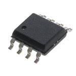
| 供应商器件封装 | 8-SO |
| 其它名称 | 596-1287-5 |
| 包装 | 管件 |
| 商标 | Power Integrations |
| 安装类型 | 表面贴装 |
| 安装风格 | SMD/SMT |
| 封装 | Tube |
| 封装/外壳 | 8-SOIC(0.154",3.90mm 宽) |
| 封装/箱体 | SOIC-8 |
| 工作温度范围 | 0 C to + 105 C |
| 工厂包装数量 | 100 |
| 应用 | 转换器,ACDC |
| 标准包装 | 100 |
| 特色产品 | http://www.digikey.com/cn/zh/ph/PI/CapZero.html |
| 类型 | 电容器放电 |
| 输入电压范围 | 825 V |
| 输入电流 | 21.7 uA |


- 商务部:美国ITC正式对集成电路等产品启动337调查
- 曝三星4nm工艺存在良率问题 高通将骁龙8 Gen1或转产台积电
- 太阳诱电将投资9.5亿元在常州建新厂生产MLCC 预计2023年完工
- 英特尔发布欧洲新工厂建设计划 深化IDM 2.0 战略
- 台积电先进制程称霸业界 有大客户加持明年业绩稳了
- 达到5530亿美元!SIA预计今年全球半导体销售额将创下新高
- 英特尔拟将自动驾驶子公司Mobileye上市 估值或超500亿美元
- 三星加码芯片和SET,合并消费电子和移动部门,撤换高东真等 CEO
- 三星电子宣布重大人事变动 还合并消费电子和移动部门
- 海关总署:前11个月进口集成电路产品价值2.52万亿元 增长14.8%


PDF Datasheet 数据手册内容提取
CAPZero Family Zero1 Loss Automatic X Capacitor Discharge IC Product Highlights • Blocks current through X capacitor discharge resistors when AC R1 voltage is connected D1 • Automatically discharges X capacitors through discharge resistors when AC is disconnected • Simplifies EMI filter design – larger X capacitor allows smaller MOV inductive components with no change in consumption AC X Capacitor aEnMdI OFtilhteerr • Only two terminals – meets safety standards for use before or after Components system input fuse • >4 mm creepage on package and PCB D2 • Self supplied – no external bias required CAPZero • High common mode surge immunity – no external ground R2 connection PI-6599-110711 • High differential surge withstand – 1000 V internal MOSFETs Figure 1. Typical Application – Not a Simplified Circuit. EcoSmart™– Energy Efficient • <5 mW consumption at 230 VAC for all X capacitor values Applications Component Selection Table • All ACDC converters with X capacitors >100 nF • Appliances requiring EuP Lot 6 compliance Total Series Maximum Total • Adapters requiring ultra low no-load consumption Product4 BV Resistance2 DSS X Capacitance • All converters requiring very low standby power (R1 + R2) Description CAP002DG 825 V ≤500 nF 1.5 MW CAP012DG 1000 V When AC voltage is applied, CAPZero™ blocks current flow in the X capacitor safety discharge resistors, reducing the power loss to less CAP003DG 825 V 750 nF 1.02 MW than 5 mW, or essentially zero1 at 230 VAC. When AC voltage is CAP013DG 1000 V disconnected, CAPZero automatically discharges the X capacitor by CAP004DG 825 V connecting the series discharge resistors. This operation allows total 1 mF 780 kW flexibility in the choice of the X capacitor to optimize differential mode CAP014DG 1000 V EMI filtering and reduce inductor costs, with no change in power CAP005DG 825 V consumption. 1.5 mF 480 kW CAP015DG 1000 V Designing with CAPZero is simply a matter of selecting the appropriate CAP006DG 825 V CAPZero device and external resistor values in Table 1 for the 2 mF 360 kW X capacitor value being used. This design choice will provide a worst CAP016DG 1000 V case RC time constant, when the AC supply is disconnected, of less CAP007DG 825 V than 1 second as required by international safety standards. 2.5 mF 300 kW CAP017DG 1000 V The simplicity and ruggedness of the two terminal CAPZero IC makes it CAP008DG 825 V an ideal choice in systems designed to meet EuP Lot 6 requirements. 3.5 mF 200 kW CAP018DG 1000 V The CAPZero family has two voltage grades: 825 V and 1000 V. The CAP009DG 825 V voltage rating required depends on surge requirement and circuit 5 mF 150 kW3 CAP019DG 1000 V configuration of the application. See Key Applications Considerations section for details. Table 1. Component Selection Table. Notes: 1. IEC 62301 clause 4.5 rounds standby power use below 5 mW to zero. 2. Values are nominal. RC time constant is <1 second with ±20% X capacitor and ±5% resistance from these nominal values. 3. Lowest value of discharge resistor that can be used. 4. Packages: D: SO-8. www.power.com March 2018
CAPZero Pin Functional Description For MOV placement that is not directly across the X Capacitor1 (for example MOV in Figure 3) the 1000 V CAPZero devices can be The pin configuration of Figure 2 ensures that the width of the SO-8 used up to a sPuOrSg2e specification of 1.5 kV. For differential surge package is used to provide creepage and clearance distance of over voltage specifications of >1.5 kV it is recommended that the MOV is 4 mm. always placed in the location shown in Figure 3 as MOV . POS1 Although electrical connections are only made to pins 2, 3, 6 and 7, it It is always recommended that the peak voltage between terminals is recommended that pins 1-4 and pins 5-8 are coupled together on D1 and D2 of CAPZero is measured during surge tests in the final the PCB – see Applications Section. system. Measurements of peak voltage across CAPZero during surge tests should be made with oscilloscope probes having appropriate voltage rating and using an isolated supply to the oscilloscope to avoid ground currents influencing measurement results. When making such measurements, it is recommended that 50 V engineer- D Package (SO-8) ing margin is allowed below the breakdown voltage specification (for example 950 V with the 1000 V CAPZero). 1 8 NC NC If the measured peak Drain voltage exceeds 950 V, an external 1 kV D1 2 7 D2 ceramic capacitor can be placed between D1 and D2 terminals to attenuate the voltage applied between the CAPZero terminals during 3 6 D1 D2 surge. Please refer to the Application Note AN-48 for the details. 4 5 This optional external capacitor placement is shown as C in Figure NC NC EXT 3. It should be noted that use of an external capacitor in this way will increase power consumption slightly due to the C charge/discharge EXT currents flowing in R1 and R2 while AC is connected. PI-5608-060810 PCB Layout and External Resistor Selection Figure 4 shows a typical PCB layout configuration for CAPZero. The Figure 2. Pin Configuration. external resistors in this case are divided into two separate surface mount resistors to distribute loss under fault conditions – for example Key Application Considerations where a short-circuit exists between CAPZero terminals D1 and D2. R1 and R2 values are selected according to Table 1. Breakdown Voltage Selection Figure 3 illustrates possible system configurations influencing the Under a fault condition where CAPZero terminals D1 and D2 are choice of CAPZero breakdown voltage. The system configuration shorted together, each resistor will dissipate a power that can be variables include the placement of the system MOV and X capacitor(s) calculated from the applied AC voltage and the R1 and R2 values. For as well as the differential surge voltage specifications of the example in an application using CAP004 or CAP014, R1=R2=390 kW. If CAPZero is shorted out at 265 VAC R1 and R2 will each dissipate application. 45 mW. As shown in Table 1, each device in the CAPZero family has a 825 V Resistors R1 and R2 should also be rated for 50% of the system input or 1000 V option. For applications where the system MOV is placed voltage again to allow for the short-circuitry of CAPZero D1 to D2 pins in position 1 (MOV in Figure 3), the 825 V option will typically POS1 during single point fault testing. provide adequate voltage withstand for surge requirements up to 3 kV or more. The 1 kV CAPZero would be recommended for higher surge requirements or if additional voltage margin is required. R1 D1 MOV MOV POS1 POS2 C Other EMI AC EXT Filter Components X Capacitor1 X Capacitor2 CAPZero D2 R2 PI-6600-110711 Figure 3. Placement Options of MOV and C . EXT 2 Rev. H 03/18 www.power.com
CAPZero If lower dissipation or lower voltage across each resistor is required during fault tests, the total external resistance can be divided into more discrete resistors, however the total resistance must be equal to that specified in Table 1. Safety CAPZero meets safety requirements even if placed before the system X Capacitor input fuse. If a short-circuit is placed between D1 and D2 terminals R1 of CAPZero, the system is identical to existing systems where CAPZero is not used. With regard to open circuit tests, it is not possible to create a fault condition through a single pin fault (for example lifted pin test) since there are two pins connected to each of D1 and D2. If several pins are lifted to create an open circuit, the condition is identical to an open circuit X capacitor discharge resistor in existing systems where CAPZero is not used. If redundancy against open circuit faults is required, two CAPZero and R1 / R2 configurations can be placed in R2 (cid:31)≥4 mm parallel. Discharge Operation To meet the safety regulations, when the AC supply is disconnected, CAPZero will discharge the X capacitor to the safety extra low voltage (SELV) levels according to the above functional description. Although there are no specific safety requirements below SELV, CAPZero still PI-5610-041310 continues the discharge until the X capacitor is fully discharged. As such CAPZero can be safely used at low input voltages such as the Figure 4. Typical PCB Layout. common industrial 18 VAC and 24 VAC supply rails while retaining X capacitor discharge when the AC source is disconnected. 3 www.power.com Rev. H 03/18
CAPZero Absolute Maximum Ratings(4) DRAIN Pin Voltage(1) CAP002-CAP009 ..............................825 V Operating Ambient Temperature .............................-10 °C to 105 °C CAP012-CAP019 .............................1000 V Maximum Junction Temperature .............................-10 °C to 110 °C DRAIN Peak Current(2) CAP002/CAP012 ...........................0.553 mA Notes: CAP003/CAP013 ...........................0.784 mA 1. Voltage of D1 pin relative to D2 pin in either polarity. CAP004/CAP014 ...........................1.026 mA 2. The peak DRAIN current is allowed while the DRAIN voltage is CAP005/CAP015 ...........................1.667 mA simultaneously less than 400 V. CAP006/CAP016 ...........................2.222 mA 3. 1/16 in. from case for 5 seconds. CAP007/CAP017 ............................2.667 mA 4. The Absolute Maximum Ratings specified may be applied one at CAP008/CAP018 ...........................4.000 mA a time without causing permanent damage to the product. CAP009/CAP019 ...........................5.333 mA Exposure to Absolute Maximum Rating conditions for extended Storage Temperature ..............................................-65 °C to 150 °C periods of time may affect product reliability. Lead Temperature(3) ..............................................................260 °C Thermal Resistance Thermal Resistance: D Package1: Notes: (q ) .................160 °C/W (Single layer JEDEC PCB) 1. Reference thermal resistance test conditions: JEDEC JA (q ) ..........................................40 °C/W (Bottom) JESD51-3, SEMI Test Method #G43-87, and MIL-STD-883 JC (q ) ...............................................75 °C/W (Top) Method 10121.1. JC Conditions Parameter Symbol T = -10 to 105 °C Min Typ Max Units A (Unless Otherwise Specified) Control Functions AC Removal t Line Cycle Frequency 47-63 Hz 22 31.4 ms Detection Time DETECT CAP002/012 0.25 CAP003/013 0.37 CAP004/014 0.48 CAP005/015 0.78 Drain Saturation I mA CurrentA,B DSAT CAP006/016 1.04 CAP007/017 1.25 CAP008/018 1.88 CAP009/019 2.5 Supply Current I T = 25 °C 21.7 mA SUPPLY A Notes: A. Saturation current specifications ensure a natural RC discharge characteristic at all voltages up to 265 VAC pk with the external resistor values specified in Component Selection Table 1. B. Specifications are guaranteed by characterization and design. 4 Rev. H 03/18 www.power.com
CAPZero Typical Performance Characteristics 1.20 0 1 1 2 1.10 06 0- 2 0 1.00 PI-6 C) 0.90 ° 5 2 0.80 o d t 0.70 e z ali 0.60 m r o 0.50 N ( LY 0.40 P P SU 0.30 I 0.20 0.10 0.00 -25 0 25 50 75 100 125 Temperature (°C) Figure 5. I vs. Temperature. SUPPLY 5 www.power.com Rev. H 03/18
CAPZero SO-8 (D Package) 0.10 (0.004) C A-B 2X 2 DETAIL A 4 B 4.90 (0.193) BSC A 4 D 8 5 GAUGE PLANE SEATING PLANE 2 3.90 (0.154) BSC 6.00 (0.236) BSC C 0 - 8o 0.25 (0.010) 1.04 (0.041) REF BSC 0.10 (0.004) CD 0.40 (0.016) 2X Pin 1 ID 1 4 0.20 (0.008) C 1.27 (0.050) 1.27 (0.050) BSC 2X 7X 0.31 - 0.51 (0.012 - 0.020) 0.25 (0.010) M CA-BD 1.35 (0.053) 1.25 - 1.65 1.75 (0.069) (0.049 - 0.065) DETAIL A 0.10 (0.004) 0.10 (0.004) C H 0.25 (0.010) 7X SEATING PLANE 0.17 (0.007) C 0.25 (0.010) Reference Solder Pad + Dimensions Notes: 1. JEDEC reference: MS-012. 1.45 (0.057) 4.00 (0.157) 5.45 (0.215) 2. Package outline exclusive of mold flash and metal burr. 3. Package outline inclusive of plating thickness. 4. Datums A and B to be determined at datum plane H. + + + 5. Controlling dimensions are in millimeters. Inch dimensions are shown in parenthesis. Angles in degrees. 1.27 (0.050) 0.60 (0.024) D08A PI-5615-041210 Part Ordering Information • CAPZero Product Family • 002 Series Number • Package Identifier D Plastic SO-8 • Package Material G GREEN: Halogen Free and RoHS Compliant • Tape & Reel and Other Options Blank Standard Configurations CAP 002 D G - TL TL Tape & Reel, 2.5 k pcs. 6 Rev. H 03/18 www.power.com
CAPZero Revision Notes Date A Code A release. 04/14/10 B Updated I condition. Added figure 5. Parameter T was updated. 06/08/10 SUPPLY DETECT Updated Table 1. Updated Note 1 in Table 1. Added “Discharge Operation” paragraph. Updated Absolute Maximum C 02/11 Ratings Table. C Added Maximum Junction Temperature specification. 04/11 D Updated Figures 1 and 3. 11/07/11 E Added R max. at 105 °C for CAPZero parts. 03/12 DS(ON) E Added Thermal Resistance section. 09/16/13 F Updated with new Brand Style. 05/15 G Removed R information. 07/15 DS(ON) H Added Note 3 in Table 1. Updated text on page 2, 3rd paragraph right column. 03/18 7 www.power.com Rev. H 03/18
For the latest updates, visit our website: www.power.com Power Integrations reserves the right to make changes to its products at any time to improve reliability or manufacturability. Power Integrations does not assume any liability arising from the use of any device or circuit described herein. POWER INTEGRATIONS MAKES NO WARRANTY HEREIN AND SPECIFICALLY DISCLAIMS ALL WARRANTIES INCLUDING, WITHOUT LIMITATION, THE IMPLIED WARRANTIES OF MERCHANTABILITY, FITNESS FOR A PARTICULAR PURPOSE, AND NON-INFRINGEMENT OF THIRD PARTY RIGHTS. Patent Information The products and applications illustrated herein (including transformer construction and circuits external to the products) may be covered by one or more U.S. and foreign patents, or potentially by pending U.S. and foreign patent applications assigned to Power Integrations. A complete list of Power Integrations patents may be found at www.power.com. Power Integrations grants its customers a license under certain patent rights as set forth at www.power.com/ip.htm. Life Support Policy POWER INTEGRATIONS PRODUCTS ARE NOT AUTHORIZED FOR USE AS CRITICAL COMPONENTS IN LIFE SUPPORT DEVICES OR SYSTEMS WITHOUT THE EXPRESS WRITTEN APPROVAL OF THE PRESIDENT OF POWER INTEGRATIONS. As used herein: 1. A Life support device or system is one which, (i) is intended for surgical implant into the body, or (ii) supports or sustains life, and (iii) whose failure to perform, when properly used in accordance with instructions for use, can be reasonably expected to result in significant injury or death to the user. 2. A critical component is any component of a life support device or system whose failure to perform can be reasonably expected to cause the failure of the life support device or system, or to affect its safety or effectiveness. The PI logo, TOPSwitch, TinySwitch, SENZero, SCALE, SCALE-iDriver, SCALE-iFlex, Qspeed, PeakSwitch, LYTSwitch, LinkZero, LinkSwitch, InnoSwitch, HiperTFS, HiperPFS, HiperLCS, DPA-Switch, CAPZero, Clampless, EcoSmart, E-Shield, Filterfuse, FluxLink, StakFET, PI Expert and PI FACTS are trademarks of Power Integrations, Inc. Other trademarks are property of their respective companies. ©2018, Power Integrations, Inc. Power Integrations Worldwide Sales Support Locations World Headquarters Germany (AC-DC/LED Sales) Italy Singapore 5245 Hellyer Avenue Lindwurmstrasse 114 Via Milanese 20, 3rd. Fl. 51 Newton Road San Jose, CA 95138, USA D-80337 München 20099 Sesto San Giovanni (MI) Italy #19-01/05 Goldhill Plaza Main: +1-408-414-9200 Germany Phone: +39-024-550-8701 Singapore, 308900 Customer Service: Phone: +49-89-5527-39100 e-mail: eurosales@power.com Phone: +65-6358-2160 Worldwide: +1-65-635-64480 e-mail: eurosales@power.com e-mail: singaporesales@power.com Japan Americas: +1-408-414-9621 Germany (Gate Driver Sales) Yusen Shin-Yokohama 1-chome Bldg. Taiwan e-mail: usasales@power.com HellwegForum 1 1-7-9, Shin-Yokohama, Kohoku-ku 5F, No. 318, Nei Hu Rd., Sec. 1 China (Shanghai) 59469 Ense Yokohama-shi, Nei Hu Dist. Rm 2410, Charity Plaza, No. 88 Germany Kanagawa 222-0033 Japan Taipei 11493, Taiwan R.O.C. North Caoxi Road Tel: +49-2938-64-39990 Phone: +81-45-471-1021 Phone: +886-2-2659-4570 Shanghai, PRC 200030 e-mail: igbt-driver.sales@power.com e-mail: japansales@power.com e-mail: taiwansales@power.com Phone: +86-21-6354-6323 India Korea UK e-mail: chinasales@power.com #1, 14th Main Road RM 602, 6FL Building 5, Suite 21 China (Shenzhen) Vasanthanagar Korea City Air Terminal B/D, 159-6 The Westbrook Centre 17/F, Hivac Building, No. 2, Keji Nan Bangalore-560052 India Samsung-Dong, Kangnam-Gu, Milton Road 8th Road, Nanshan District, Phone: +91-80-4113-8020 Seoul, 135-728, Korea Cambridge Shenzhen, China, 518057 e-mail: indiasales@power.com Phone: +82-2-2016-6610 CB4 1YG Phone: +86-755-8672-8689 e-mail: koreasales@power.com Phone: +44 (0) 7823-557484 e-mail: chinasales@power.com e-mail: eurosales@power.com