ICGOO在线商城 > 分立半导体产品 > 晶体管 - 双极 (BJT) - 单 > BCW60D,215
 Datasheet下载
- 型号: BCW60D,215
- 制造商: NXP Semiconductors
- 库位|库存: xxxx|xxxx
- 要求:
| 数量阶梯 | 香港交货 | 国内含税 |
| +xxxx | $xxxx | ¥xxxx |
查看当月历史价格
查看今年历史价格
BCW60D,215产品简介:
ICGOO电子元器件商城为您提供BCW60D,215由NXP Semiconductors设计生产,在icgoo商城现货销售,并且可以通过原厂、代理商等渠道进行代购。 BCW60D,215价格参考¥0.19-¥0.19。NXP SemiconductorsBCW60D,215封装/规格:晶体管 - 双极 (BJT) - 单, 双极 (BJT) 晶体管 NPN 32V 100mA 250MHz 250mW 表面贴装 TO-236AB。您可以下载BCW60D,215参考资料、Datasheet数据手册功能说明书,资料中有BCW60D,215 详细功能的应用电路图电压和使用方法及教程。
BCW60D,215 是 Nexperia USA Inc. 生产的一款双极型晶体管(BJT),属于单晶体管类型。它广泛应用于各种电子电路中,尤其是在低功耗和高可靠性要求的场景下。以下是该型号晶体管的一些典型应用场景:

 1. 电源管理
BCW60D,215 常用于电源管理电路中,作为开关或线性稳压器的控制元件。它可以有效地调节电流和电压,确保输出稳定,适用于电池供电设备、充电器等。

 2. 信号放大
该晶体管可用于音频放大器、传感器信号放大等场景。由于其低噪声特性和较高的增益,能够在保持信号完整性的前提下进行有效的放大操作。

 3. 开关应用
在数字电路中,BCW60D,215 可以用作开关元件,控制负载的通断。例如,在继电器驱动、LED 驱动等场合,它能够快速响应并提供稳定的开关性能。

 4. 电机控制
在小型电机控制中,该晶体管可以作为驱动元件,控制电机的启动、停止及速度调节。其高可靠性和低功耗特性使其适合用于微控制器外围电路中的电机驱动。

 5. 保护电路
BCW60D,215 还可以用于过流保护、短路保护等安全电路中。通过检测异常电流,及时切断电路,防止损坏其他元器件。

 6. 通信设备
在通信设备中,如调制解调器、无线发射模块等,BCW60D,215 可用于信号处理和功率放大,确保信号传输的稳定性和可靠性。

 7. 消费电子
在智能手机、平板电脑、智能家居设备等消费电子产品中,BCW60D,215 被广泛应用于背光驱动、按键检测等低功耗需求的场景。

 总结
BCW60D,215 晶体管凭借其优异的性能和可靠性,适用于多种低功耗、高精度的电子电路设计。无论是电源管理、信号放大还是开关控制,它都能提供稳定且高效的工作表现。
| 参数 | 数值 |
| 产品目录 | |
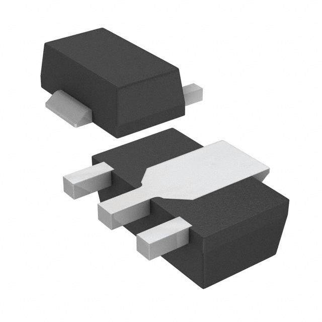
| 描述 | TRANSISTOR NPN 32V 100MA SOT23两极晶体管 - BJT TRANS GP TAPE-7 |
| 产品分类 | 晶体管(BJT) - 单路分离式半导体 |
| 品牌 | NXP Semiconductors |
| 产品手册 | |
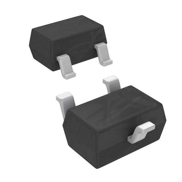
| 产品图片 |
|
| rohs | 符合RoHS无铅 / 符合限制有害物质指令(RoHS)规范要求 |
| 产品系列 | 晶体管,两极晶体管 - BJT,NXP Semiconductors BCW60D,215- |
| 数据手册 | |
| 产品型号 | BCW60D,215 |
| PCN封装 | |
| PCN设计/规格 | |
| 不同 Ib、Ic时的 Vce饱和值(最大值) | 550mV @ 1.25mA,50mA |
| 不同 Ic、Vce 时的DC电流增益(hFE)(最小值) | 380 @ 2mA,5V |
| 产品种类 | 两极晶体管 - BJT |
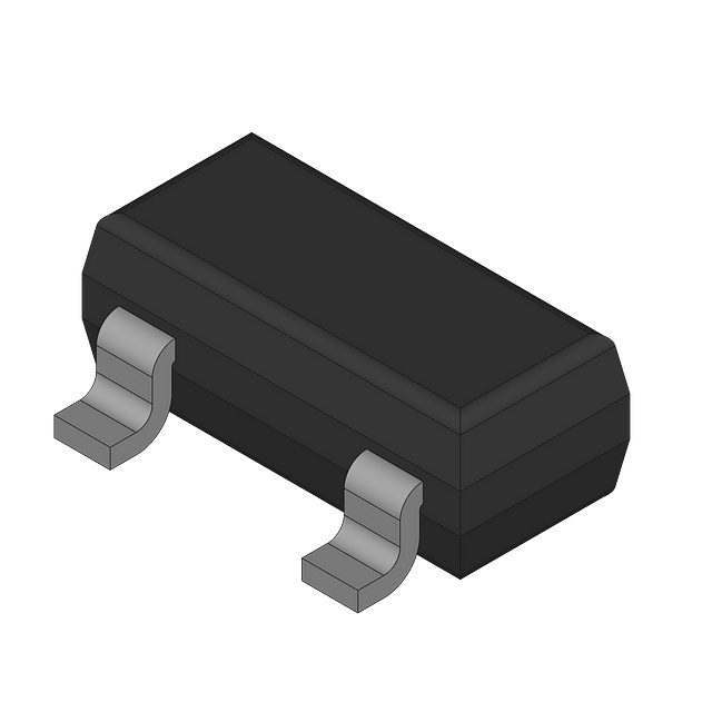
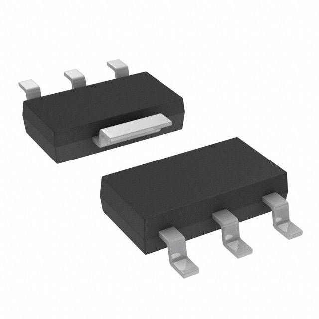
| 供应商器件封装 | SOT-23 (TO-236AB) |
| 其它名称 | 568-6122-2 |
| 功率-最大值 | 250mW |
| 包装 | 带卷 (TR) |
| 发射极-基极电压VEBO | 5 V |
| 商标 | NXP Semiconductors |
| 增益带宽产品fT | 250 MHz |
| 安装类型 | 表面贴装 |
| 安装风格 | SMD/SMT |
| 封装 | Reel |
| 封装/外壳 | TO-236-3,SC-59,SOT-23-3 |
| 封装/箱体 | SOT-23 |
| 工厂包装数量 | 3000 |
| 晶体管极性 | NPN |
| 晶体管类型 | NPN |
| 最大功率耗散 | 250 mW |
| 最大工作温度 | + 150 C |
| 最大直流电集电极电流 | 0.1 A |
| 最小工作温度 | - 65 C |
| 标准包装 | 3,000 |
| 特色产品 | http://www.digikey.com/cn/zh/ph/NXP/I2C.html |
| 电压-集射极击穿(最大值) | 32V |
| 电流-集电极(Ic)(最大值) | 100mA |
| 电流-集电极截止(最大值) | - |
| 直流电流增益hFE最大值 | 100 at 10 uA at 5 V |
| 直流集电极/BaseGainhfeMin | 100 at 10 uA at 5 V, 380 at 2 mA at 5 V, 100 at 50 mA at 1 V |
| 配置 | Single |
| 集电极—发射极最大电压VCEO | 32 V |
| 集电极—基极电压VCBO | 32 V |
| 零件号别名 | BCW60D T/R |
| 频率-跃迁 | 250MHz |


- 商务部:美国ITC正式对集成电路等产品启动337调查
- 曝三星4nm工艺存在良率问题 高通将骁龙8 Gen1或转产台积电
- 太阳诱电将投资9.5亿元在常州建新厂生产MLCC 预计2023年完工
- 英特尔发布欧洲新工厂建设计划 深化IDM 2.0 战略
- 台积电先进制程称霸业界 有大客户加持明年业绩稳了
- 达到5530亿美元!SIA预计今年全球半导体销售额将创下新高
- 英特尔拟将自动驾驶子公司Mobileye上市 估值或超500亿美元
- 三星加码芯片和SET,合并消费电子和移动部门,撤换高东真等 CEO
- 三星电子宣布重大人事变动 还合并消费电子和移动部门
- 海关总署:前11个月进口集成电路产品价值2.52万亿元 增长14.8%


PDF Datasheet 数据手册内容提取
Important notice Dear Customer, On 7 February 2017 the former NXP Standard Product business became a new company with the tradename Nexperia. Nexperia is an industry leading supplier of Discrete, Logic and PowerMOS semiconductors with its focus on the automotive, industrial, computing, consumer and wearable application markets In data sheets and application notes which still contain NXP or Philips Semiconductors references, use the references to Nexperia, as shown below. Instead of http://www.nxp.com, http://www.philips.com/ or http://www.semiconductors.philips.com/, use http://www.nexperia.com Instead of sales.addresses@www.nxp.com or sales.addresses@www.semiconductors.philips.com, use salesaddresses@nexperia.com (email) Replace the copyright notice at the bottom of each page or elsewhere in the document, depending on the version, as shown below: - © NXP N.V. (year). All rights reserved or © Koninklijke Philips Electronics N.V. (year). All rights reserved Should be replaced with: - © Nexperia B.V. (year). All rights reserved. If you have any questions related to the data sheet, please contact our nearest sales office via e-mail or telephone (details via salesaddresses@nexperia.com). Thank you for your cooperation and understanding, Kind regards, Team Nexperia
DISCRETE SEMICONDUCTORS DATA SHEET dbook, halfpage M3D088 BCW60 series NPN general purpose transistors Product data sheet 1999 Apr 22 Supersedes data of 1997 Mar 10
NXP Semiconductors Product data sheet NPN general purpose transistors BCW60 series FEATURES PINNING • Low current (max. 100 mA) PIN DESCRIPTION • Low voltage (max. 32 V). 1 base 2 emitter APPLICATIONS 3 collector • General purpose switching and amplification. DESCRIPTION handbook, halfpage 3 3 NPN transistor in a SOT23 plastic package. PNP complements: BCW61 series. 1 MARKING 2 1 2 TYPE NUMBER MARKING CODE(1) BCW60B AB∗ Top view MAM255 BCW60C AC∗ BCW60D AD∗ Fig.1 Simplified outline (SOT23) and symbol. Note 1. ∗ = p : Made in Hong Kong. ∗ = t : Made in Malaysia. LIMITING VALUES In accordance with the Absolute Maximum Rating System (IEC 134). SYMBOL PARAMETER CONDITIONS MIN. MAX. UNIT V collector-base voltage open emitter − 32 V CBO V collector-emitter voltage open base − 32 V CEO V emitter-base voltage open collector − 5 V EBO I collector current (DC) − 100 mA C I peak collector current − 200 mA CM I peak base current − 200 mA BM P total power dissipation T ≤ 25 °C − 250 mW tot amb T storage temperature −65 +150 °C stg T junction temperature − 150 °C j T operating ambient temperature −65 +150 °C amb 1999 Apr 22 2
NXP Semiconductors Product data sheet NPN general purpose transistors BCW60 series THERMAL CHARACTERISTICS SYMBOL PARAMETER CONDITIONS VALUE UNIT R thermal resistance from junction to ambient note 1 500 K/W th j-a Note 1. Transistor mounted on an FR4 printed-circuit board. CHARACTERISTICS T = 25 °C unless otherwise specified. amb SYMBOL PARAMETER CONDITIONS MIN. TYP. MAX. UNIT I collector cut-off current I = 0; V = 32 V − − 20 nA CBO E CB I = 0; V = 32 V; T = 150 °C − − 20 μA E CB amb I emitter cut-off current I = 0; V = 4 V − − 20 nA EBO C EB h DC current gain I = 10 μA; V = 5 V FE C CE BCW60B 20 − − BCW60C 40 − − BCW60D 100 − − DC current gain I = 2 mA; V = 5 V C CE BCW60B 180 − 310 BCW60C 250 − 460 BCW60D 380 − 630 DC current gain I = 50 mA; V = 1 V C CE BCW60B 70 − − BCW60C 90 − − BCW60D 100 − − V collector-emitter saturation I = 10 mA; I = 0.25 mA 50 − 350 mV CEsat C B voltage I = 50 mA; I = 1.25 mA 100 − 550 mV C B V base-emitter saturation voltage I = 10 mA; I = 0.25 mA 600 − 850 mV BEsat C B I = 50 mA; I = 1.25 mA 0.7 − 1.05 V C B V base-emitter voltage I = 10 μA; V = 5 V − 520 − mV BE C CE I = 2 mA; V = 5 V 550 650 750 mV C CE I = 50 mA; V = 1 V − 780 − mV C CE C collector capacitance I = i = 0; V = 10 V; f = 1 MHz − 1.7 − pF c E e CB C emitter capacitance I = i = 0; V = 0.5 V; f = 1 MHz − 11 − pF e C c EB f transition frequency I = 10 mA; V = 5 V; 100 250 − MHz T C CE f = 100 MHz; note 1 F noise figure I = 200 μA; V = 5 V; − 2 6 dB C CE R = 2 kΩ; f = 1 kHz; B = 200 Hz S Note 1. Pulse test: t ≤ 300 μs; δ ≤ 0.02. p 1999 Apr 22 3
NXP Semiconductors Product data sheet NPN general purpose transistors BCW60 series PACKAGE OUTLINE Plastic surface mounted package; 3 leads SOT23 D B E A X HE v M A 3 Q A A1 1 2 c e1 bp w M B Lp e detail X 0 1 2 mm scale DIMENSIONS (mm are the original dimensions) UNIT A mAa1x. bp c D E e e1 HE Lp Q v w 1.1 0.48 0.15 3.0 1.4 2.5 0.45 0.55 mm 0.1 1.9 0.95 0.2 0.1 0.9 0.38 0.09 2.8 1.2 2.1 0.15 0.45 OUTLINE REFERENCES EUROPEAN ISSUE DATE VERSION IEC JEDEC EIAJ PROJECTION 97-02-28 SOT23 TO-236AB 99-09-13 1999 Apr 22 4
NXP Semiconductors Product data sheet NPN general purpose transistors BCW60 series DATA SHEET STATUS DOCUMENT PRODUCT DEFINITION STATUS(1) STATUS(2) Objective data sheet Development This document contains data from the objective specification for product development. Preliminary data sheet Qualification This document contains data from the preliminary specification. Product data sheet Production This document contains the product specification. Notes 1. Please consult the most recently issued document before initiating or completing a design. 2. The product status of device(s) described in this document may have changed since this document was published and may differ in case of multiple devices. The latest product status information is available on the Internet at URL http://www.nxp.com. DISCLAIMERS above those given in the Characteristics sections of this document is not implied. Exposure to limiting values for General ⎯ Information in this document is believed to be extended periods may affect device reliability. accurate and reliable. However, NXP Semiconductors does not give any representations or warranties, Terms and conditions of sale ⎯ NXP Semiconductors expressed or implied, as to the accuracy or completeness products are sold subject to the general terms and of such information and shall have no liability for the conditions of commercial sale, as published at consequences of use of such information. http://www.nxp.com/profile/terms, including those pertaining to warranty, intellectual property rights Right to make changes ⎯ NXP Semiconductors infringement and limitation of liability, unless explicitly reserves the right to make changes to information otherwise agreed to in writing by NXP Semiconductors. In published in this document, including without limitation case of any inconsistency or conflict between information specifications and product descriptions, at any time and in this document and such terms and conditions, the latter without notice. This document supersedes and replaces all will prevail. information supplied prior to the publication hereof. No offer to sell or license ⎯ Nothing in this document Suitability for use ⎯ NXP Semiconductors products are may be interpreted or construed as an offer to sell products not designed, authorized or warranted to be suitable for that is open for acceptance or the grant, conveyance or use in medical, military, aircraft, space or life support implication of any license under any copyrights, patents or equipment, nor in applications where failure or malfunction other industrial or intellectual property rights. of an NXP Semiconductors product can reasonably be expected to result in personal injury, death or severe Export control ⎯ This document as well as the item(s) property or environmental damage. NXP Semiconductors described herein may be subject to export control accepts no liability for inclusion and/or use of NXP regulations. Export might require a prior authorization from Semiconductors products in such equipment or national authorities. applications and therefore such inclusion and/or use is at Quick reference data ⎯ The Quick reference data is an the customer’s own risk. extract of the product data given in the Limiting values and Applications ⎯ Applications that are described herein for Characteristics sections of this document, and as such is any of these products are for illustrative purposes only. not complete, exhaustive or legally binding. NXP Semiconductors makes no representation or warranty that such applications will be suitable for the specified use without further testing or modification. Limiting values ⎯ Stress above one or more limiting values (as defined in the Absolute Maximum Ratings System of IEC 60134) may cause permanent damage to the device. Limiting values are stress ratings only and operation of the device at these or any other conditions 1999 Apr 22 5
NXP Semiconductors Customer notification This data sheet was changed to reflect the new company name NXP Semiconductors, including new legal definitions and disclaimers. No changes were made to the technical content, except for package outline drawings which were updated to the latest version. Contact information For additional information please visit: http://www.nxp.com For sales offices addresses send e-mail to: salesaddresses@nxp.com © NXP B.V. 2009 All rights are reserved. Reproduction in whole or in part is prohibited without the prior written consent of the copyright owner. The information presented in this document does not form part of any quotation or contract, is believed to be accurate and reliable and may be changed without notice. No liability will be accepted by the publisher for any consequence of its use. Publication thereof does not convey nor imply any license under patent- or other industrial or intellectual property rights. Printed in The Netherlands 115002/00/03/pp6 Date of release: 1999 Apr 22 Document order number: 9397 750 05715