ICGOO在线商城 > 射频/IF 和 RFID > RF 其它 IC 和模块 > AD630BDZ
 Datasheet下载
- 型号: AD630BDZ
- 制造商: Analog
- 库位|库存: xxxx|xxxx
- 要求:
| 数量阶梯 | 香港交货 | 国内含税 |
| +xxxx | $xxxx | ¥xxxx |
查看当月历史价格
查看今年历史价格
AD630BDZ产品简介:
ICGOO电子元器件商城为您提供AD630BDZ由Analog设计生产,在icgoo商城现货销售,并且可以通过原厂、代理商等渠道进行代购。 AD630BDZ价格参考。AnalogAD630BDZ封装/规格:RF 其它 IC 和模块, RF IC Modulator/Demodulator General Purpose 0Hz ~ 2MHz 20-CDIP。您可以下载AD630BDZ参考资料、Datasheet数据手册功能说明书,资料中有AD630BDZ 详细功能的应用电路图电压和使用方法及教程。
AD630BDZ 是由 Analog Devices Inc.(亚德诺半导体)生产的一款高性能模拟信号处理芯片,属于 RF 其他 IC 和模块分类。其主要应用场景包括以下领域:

1. 工业自动化与控制
   AD630BDZ 可用于工业自动化系统中的信号调理和数据采集。它能够处理复杂的模拟信号转换任务,例如将传感器输出的微弱信号进行放大、滤波和调制,以适应后续数字处理的需求。

2. 通信设备
   在射频(RF)和其他通信相关应用中,AD630BDZ 可作为信号调制解调的核心组件。例如,在无线通信系统中,它可以实现频率变换、混频或解调功能,支持 AM、FM 或 SSB 等调制方式。

3. 医疗设备
   该芯片适用于需要高精度信号处理的医疗设备,如心电图(ECG)、脑电图(EEG)或其他生物医学信号监测仪器。通过其优秀的线性度和低失真特性,可以准确地捕捉和处理人体生理信号。

4. 音频处理
   在专业音频设备中,AD630BDZ 可用于音频信号的调制和解调,例如立体声广播系统的 Pilot Tone 生成或解码。它的宽带宽和低噪声性能使其非常适合高质量音频应用。

5. 测试与测量仪器
   AD630BDZ 的高精度和灵活性使其成为测试与测量设备的理想选择,例如频谱分析仪、示波器或信号发生器。它可以帮助完成信号的精确转换和分析。

6. 航空航天与国防
   在雷达、导航和卫星通信系统中,AD630BDZ 能够提供可靠的信号处理能力,用于频率转换、信号分离或同步检测等关键任务。

总结来说,AD630BDZ 凭借其卓越的性能参数(如高输入阻抗、低失调电压和宽带宽),在需要高性能模拟信号处理的场景中具有广泛的应用价值。
| 参数 | 数值 |
| 产品目录 | |
| 描述 | IC MOD/DEMOD BAL 2MHZ 20-CDIP调节器/解调器 MODULATOR/DEMOD IC |
| 产品分类 | |
| 品牌 | Analog Devices Inc |
| 产品手册 | |
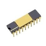
| 产品图片 |
|
| rohs | 符合RoHS无铅 / 符合限制有害物质指令(RoHS)规范要求 |
| 产品系列 | RF集成电路,调节器/解调器,Analog Devices AD630BDZ- |
| 数据手册 | |
| 产品型号 | AD630BDZ |
| RF类型 | 通用 |
| 产品种类 | 调节器/解调器 |
| 供应商器件封装 | 20-CDIP |
| 功能 | 调制器/解调器 |
| 包装 | 管件 |
| 商标 | Analog Devices |
| 安装风格 | Through Hole |
| 封装 | Tube |
| 封装/外壳 | 20-CDIP(0.300",7.62mm) |
| 封装/箱体 | CDIP-20 SB |
| 工作温度范围 | - 25 C to + 85 C |
| 工作电源电压 | +/- 15 V |
| 工厂包装数量 | 19 |
| 最大功率耗散 | 600 mW |
| 最大工作温度 | + 85 C |
| 最小工作温度 | - 25 C |
| 标准包装 | 1 |
| 电源电流 | 5 mA |
| 类型 | Modulator/Demodulator |
| 系列 | AD630 |
| 视频文件 | http://www.digikey.cn/classic/video.aspx?PlayerID=1364138032001&width=640&height=505&videoID=2245193150001 |
| 调制类型 | Balanced |
| 辅助属性 | - |
| 频率 | 0Hz ~ 2MHz |


PDF Datasheet 数据手册内容提取
Balanced Modulator/Demodulator Data Sheet AD630 FEATURES FUNCTIONAL BLOCK DIAGRAM Recovers signal from 100 dB noise CM OFF CM OFF DIFF OFF DIFF OFF ADJ ADJ ADJ ADJ 2 MHz channel bandwidth 45 V/µs slew rate BIAS Low crosstalk: −120 dB at 1 kHz, −100 dB at 10 kHz 2.5kΩ Pin programmable, closed-loop gains of ±1 and ±2 RINA AMP A CH A+ COMP 0.05% closed-loop gain accuracy and match 100 µV channel offset voltage (AD630) CH A– A +VS +VS 2.5kΩ 350 kHz full power bandwidth RINB AMP B B VOUT Chips available CH B+ 10kΩ 10kΩ APPLICATIONS CH B– –V RB 5kΩ RA Balanced modulation and demodulation RF Synchronous detection COMP CHANNEL Phase detection SEL B STATUS B/A Quadrature detection SEL A PLohcaks ein s eanmspitliivfiec adteiotenc tion –VS 00784-001 Square wave multiplication Figure 1. GENERAL DESCRIPTION Other features of the AD630 include pin programmable frequency compensation; optional input bias current compensation resistors, The AD630 is a high precision balanced modulator/demodulator common-mode and differential-offset voltage adjustment, and a that combines a flexible commutating architecture with the channel status output that indicates which of the two differential accuracy and temperature stability afforded by laser wafer trimmed inputs is active. thin film resistors. A network of on-board applications resistors provides precision closed-loop gains of ±1 and ±2 with 0.05% PRODUCT HIGHLIGHTS accuracy (AD630B). These resistors may also be used to accurately 1. The application flexibility of the AD630 makes it the best configure multiplexer gains of 1, 2, 3, or 4. External feedback choice for applications that require precisely fixed gain, enables high gain or complex switched feedback topologies. switched gain, multiplexing, integrating-switching The AD630 can be thought of as a precision op amp with two functions, and high speed precision amplification. independent differential input stages and a precision comparator 2. The 100 dB dynamic range of the AD630 exceeds that of that is used to select the active front end. The rapid response any hybrid or IC balanced modulator/demodulator and is time of this comparator coupled with the high slew rate and fast comparable to that of costly signal processing instruments. settling of the linear amplifiers minimize switching distortion. 3. The op amp format of the AD630 ensures easy implementation of high gain or complex switched feedback functions. The The AD630 is used in precision signal processing and instru- application resistors facilitate the implementation of most mentation applications that require wide dynamic range. When common applications with no additional parts. used as a synchronous demodulator in a lock-in amplifier 4. The AD630 can be used as a 2-channel multiplexer with gains configuration, the AD630 can recover a small signal from 100 dB of 1, 2, 3, or 4. The channel separation of 100 dB at 10 kHz of interfering noise (see the Lock-In Amplifier Applications approaches the limit achievable with an empty IC package. section). Although optimized for operation up to 1 kHz, the 5. Laser trimming of the comparator and amplifying channel circuit is useful at frequencies up to several hundred kilohertz. offsets eliminate the need for external nulling in most cases. Rev. G Document Feedback Irnefsopromnasitbioilnit yf uisr nasisshuemde bdy b yA Annalaolgog D Deevviciceess ifso rb ietsli euvsee,d n otor fbore a ancyc iunrfartineg aenmde nretlsi aobf lpea. tHeonwtse ovre or,t hneor One Technology Way, P.O. Box 9106, Norwood, MA 02062-9106, U.S.A. rights of third parties that may result from its use. Specifications subject to change without notice. No license is granted by implication or otherwise under any patent or patent rights of Analog Devices. Tel: 781.329.4700 ©2015–2016 Analog Devices, Inc. All rights reserved. Trademarks and registered trademarks are the property of their respective owners. Technical Support www.analog.com
AD630 Data Sheet TABLE OF CONTENTS Features .............................................................................................. 1 Circuit Description .................................................................... 13 Applications ....................................................................................... 1 Other Gain Configurations ....................................................... 14 Functional Block Diagram .............................................................. 1 Switched Input Impedance ....................................................... 14 General Description ......................................................................... 1 Frequency Compensation ......................................................... 14 Product Highlights ........................................................................... 1 Offset Voltage Nulling ............................................................... 15 Revision History ............................................................................... 2 Channel Status Output .............................................................. 15 Specifications ..................................................................................... 3 Applications Information .............................................................. 16 Absolute Maximum Ratings ............................................................ 4 Balanced Modulator ................................................................... 16 Thermal Resistance ...................................................................... 4 Balanced Demodulator .............................................................. 16 Chip Availability ........................................................................... 4 Precision Phase Comparator .................................................... 16 ESD Caution .................................................................................. 4 Precision Rectifier Absolute Value ........................................... 16 Pin Configurations and Function Descriptions ........................... 5 LVDT Signal Conditioner ......................................................... 17 Typical Performance Characteristics ............................................. 9 AC Bridge .................................................................................... 17 Test Circuits ..................................................................................... 11 Lock-In Amplifier Applications ............................................... 18 Theory of Operation ...................................................................... 12 Outline Dimensions ....................................................................... 19 Two Ways To Look At The AD630 .......................................... 12 Ordering Guide .......................................................................... 20 How the AD630 Works .............................................................. 12 REVISION HISTORY 12/2016—Rev. F to Rev. G 6/2004—Rev. D to Rev. E Changes to Figure 1 .......................................................................... 1 Changes to Ordering Guide ............................................................. 3 Changes to Figure 31 ...................................................................... 17 Replaced Figure 12 ............................................................................ 9 Changes to Figure 35 ...................................................................... 18 Changes to AC Bridge Section ......................................................... 9 Replaced Figure 13 ......................................................................... 10 7/2015—Rev. E to Rev. F Changes to Lock-In Amplifier Applications ............................... 10 Updated Format .................................................................. Universal Updated Outline Dimensions ....................................................... 11 Changes to Features Section, General Description Section, Product Highlights Section, and Figure 1 ..................................... 1 6/2001—Rev. C to Rev. D Added Applications Section ............................................................ 1 Changes to Specification Table ........................................................ 2 Changes to Table 3 ............................................................................ 4 Changes to Thermal Characteristics ............................................... 3 Added Table 4; Renumbered Sequentially .................................... 5 Changes to Ordering Guide ............................................................. 3 Added Figure 4; Renumbered Sequentially and Table 5 ............. 6 Changes to Pin Configurations ....................................................... 3 Added Figure 5 and Table 6 ............................................................. 7 Changes to Outline Dimensions .................................................. 11 Added Table 7 .................................................................................... 8 Changes to Figure 7, Figure 8, and Figure 9 ................................. 9 Changes to Figure 13, Figure 14, and Figure 15 ......................... 10 Added Test Circuits Section and Figure 16 to Figure 19 ........... 11 Added Theory of Operation Section ........................................... 12 Change to Figure 24 ....................................................................... 13 Updated Outline Dimensions ....................................................... 19 Changes to Ordering Guide .......................................................... 20 Rev. G | Page 2 of 20
Data Sheet AD630 SPECIFICATIONS At 25°C and ±V = ±15 V, unless otherwise noted. S Table 1. AD630J/AD630A AD630K/AD630B AD630S Parameter Min Typ Max Min Typ Max Min Typ Max Unit GAIN Open-Loop Gain 90 110 100 120 90 110 dB ±1, ±2 Closed-Loop Gain Error 0.1 0.05 0.1 % Closed-Loop Gain Match 0.1 0.05 0.1 % Closed-Loop Gain Drift 2 2 2 ppm/°C CHANNEL INPUTS V Operational Limit1 (−V + 4) to (+V − 1) (−V + 4) to (+V − 1) (−V + 4) to (+V − 1) V IN S S S S S S Input Offset Voltage 500 100 500 µV T to T 800 160 1000 µV MIN MAX Input Bias Current 100 300 100 300 100 300 nA Input Offset Current 10 50 10 50 10 50 nA Channel Separation at 10 kHz 100 100 100 dB COMPARATOR V Operational Limit1 (−V + 3) to (+V − 1.5) (−V + 3) to (+V − 1.5) (−V + 3) to (+V − 1.3) V IN S S S S S S Switching Window ±1.5 ±1.5 ±1.5 mV T to T ±2.0 ±2.0 ±2.5 mV MIN MAX Input Bias Current 100 300 100 300 100 300 nA Response Time (−5 mV to +5 mV Step) 200 200 200 ns Channel Status I at V = −V + 0.4 V2 1.6 1.6 1.6 mA SINK OL S Pull-Up Voltage (−V + 33) (−V + 33) (−V + 33) V S S S DYNAMIC PERFORMANCE Unity Gain Bandwidth 2 2 2 MHz Slew Rate3 45 45 45 V/µs Settling Time to 0.1% (20 V Step) 3 3 3 µs OPERATING CHARACTERISTICS Common-Mode Rejection 85 105 90 110 90 110 dB Power Supply Rejection 90 110 90 110 90 110 dB Supply Voltage Range ±5 ±16.5 ±5 ±16.5 ±5 ±16.5 V Supply Current 4 5 4 5 4 5 mA OUTPUT VOLTAGE, AT R = 2 kΩ L T to T ±10 ±10 ±10 V MIN MAX Output Short-Circuit Current 25 25 25 mA TEMPERATURE RANGES N Package 0 70 0 70 °C D Package −25 +85 −25 +85 −55 +125 °C 1 If one terminal of each differential channel or comparator input is kept within these limits the other terminal may be taken to the positive supply. 2 ISINK at VOL = (−VS + 1 V) is typically 4 mA. 3 Pin 12 open. Slew rate with Pin 12 and Pin 13 shorted is typically 35 V/µs. Rev. G | Page 3 of 20
AD630 Data Sheet ABSOLUTE MAXIMUM RATINGS CHIP AVAILABILITY Table 2. The AD630 is available in laser trimmed, passivated chip form. Parameter Rating Figure 2 shows the AD630 metallization pattern, bonding pads, Supply Voltage ±18 V and dimensions. AD630 chips are available; consult factory for Internal Power Dissipation 600 mW details. Output Short-Circuit to Ground Indefinite Storage Temperature 0.99 (2.515) Ceramic Package −65°C to +150°C 18 17 16 15 Plastic Package −55°C to +125°C 19 14 Lead Temperature Range (Soldering, 10 sec) 300°C 20 13 Maximum Junction Temperature 150°C 1 2 Stresses at or above those listed under Absolute Maximum Ratings may cause permanent damage to the product. This is a 0.089 (2.260) stress rating only; functional operation of the product at these 12 or any other conditions above those indicated in the operational section of this specification is not implied. Operation beyond 11 the maximum operating conditions for extended periods may 10 affect product reliability. 3 4 5 6 7 8 9 00784-002 THERMAL RESISTANCE Figure 2. Chip Metallization and Pinout Dimensions shown in inches and (millimeters) Table 3. Thermal Resistance Contact factory for latest dimensions Package Type θ θ Unit JC JA ESD CAUTION 20-Lead PDIP (N-20) 24 61 °C/W 20-Lead SBDIP (D-20) 35 120 °C/W 20-Lead LCC (E-20-4) 35 120 °C/W 20-Lead SOIC_W (RW-20) 38 75 °C/W Rev. G | Page 4 of 20
Data Sheet AD630 PIN CONFIGURATIONS AND FUNCTION DESCRIPTIONS RINA 1 20 CH A– CH A+ 2 19 CH B– DIFF OFF ADJ 3 18 CH B+ DIFF OFF ADJ 4 AD630 17 RINB CM OFF ADJ 5 TOP VIEW 16 RA (Not to Scale) CM OFF ADJ 6 15 RF CHANNEL STATUS B/A 7 14 RB –VS 8 13 VOUT SSEELL BA 190 1121 C+VOSMP 00784-030 Figure 3. 20-Lead SOIC Pin Configuration Table 4. 20-Lead SOIC Pin Function Descriptions Pin No. Mnemonic Description 1 R A 2.5 kΩ Resistor to Noninverting Input of Op Amp A IN 2 CH A+ Noninverting Input of Op Amp A 3 DIFF OFF ADJ Differential Offset Adjustment 4 DIFF OFF ADJ Differential Offset Adjustment 5 CM OFF ADJ Common-Mode Offset Adjustment 6 CM OFF ADJ Common-Mode Offset Adjustment 7 CHANNEL STATUS B/A B or A Channel Status 8 −V Negative Supply S 9 SEL B B Channel Comparator Input 10 SEL A A Channel Comparator Input 11 +V Positive Supply S 12 COMP Pin to Connect Internal Compensation Capacitor 13 V Output Voltage OUT 14 R 10 kΩ Gain Setting Resistor B 15 R 10 kΩ Feedback Resistor F 16 R 5 kΩ Feedback Resistor A 17 R B 2.5 kΩ Resistor to Noninverting Input of Op Amp B IN 18 CH B+ Noninverting Input of Op Amp B 19 CH B− Inverting Input of Op Amp B 20 CH A− Inverting Input of Op Amp A Rev. G | Page 5 of 20
AD630 Data Sheet RINA 1 20 CH A– CH A+ 2 19 CH B– DIFF OFF ADJ 3 18 CH B+ DIFF OFF ADJ 4 AD630 17 RINB CM OFF ADJ 5 (NToOt Pto V SIEcaWle) 16 RA CM OFF ADJ 6 15 RF CHANNEL STATUS B/A 7 14 RB –VS 8 13 VOUT SSEELL BA 190 1112 C+VOSMP 00784-031 Figure 4. 20-Lead PDIP Pin Configuration Table 5. 20-Lead PDIP Pin Function Descriptions Pin No. Mnemonic Description 1 R A 2.5 kΩ Resistor to Noninverting Input of Op Amp A IN 2 CH A+ Noninverting Input of Op Amp A 3 DIFF OFF ADJ Differential Offset Adjustment 4 DIFF OFF ADJ Differential Offset Adjustment 5 CM OFF ADJ Common-Mode Offset Adjustment 6 CM OFF ADJ Common-Mode Offset Adjustment 7 CHANNEL STATUS B/A B or A Channel Status 8 −V Negative Supply S 9 SEL B B Channel Comparator Input 10 SEL A A Channel Comparator Input 11 +V Positive Supply S 12 COMP Pin to Connect Internal Compensation Capacitor 13 V Output Voltage OUT 14 R 10 kΩ Gain Setting Resistor B 15 R 10 kΩ Feedback Resistor F 16 R 5 kΩ Feedback Resistor A 17 R B 2.5 kΩ Resistor to Noninverting Input of Op Amp B IN 18 CH B+ Noninverting Input of Op Amp B 19 CH B− Inverting Input of Op Amp B 20 CH A− Inverting Input of Op Amp A Rev. G | Page 6 of 20
Data Sheet AD630 RINA 1 20 CH A– CH A+ 2 19 CH B– DIFF OFF ADJ 3 18 CH B+ DIFF OFF ADJ 4 17 RINB CM OFF ADJ 5 AD630 16 RA CM OFF ADJ 6 (NToOt Pto V SIEcaWle)15 RF CHANNEL STATUS B/A 7 14 RB –VS 8 13 VOUT SEL B 9 12 COMP SEL A 10 11+VS 00784-003 Figure 5. 20-Lead CERDIP Pin Configuration Table 6. 20-Lead CERDIP Pin Function Descriptions Pin No. Mnemonic Description 1 R A 2.5 kΩ Resistor to Noninverting Input of Op Amp A IN 2 CH A+ Noninverting Input of Op Amp A 3 DIFF OFF ADJ Differential Offset Adjustment 4 DIFF OFF ADJ Differential Offset Adjustment 5 CM OFF ADJ Common-Mode Offset Adjustment 6 CM OFF ADJ Common-Mode Offset Adjustment 7 CHANNEL STATUS B/A B or A Channel Status 8 −V Negative Supply S 9 SEL B B Channel Comparator Input 10 SEL A A Channel Comparator Input 11 +V Positive Supply S 12 COMP Pin to Connect Internal Compensation Capacitor 13 V Output Voltage OUT 14 R 10 kΩ Gain Setting Resistor B 15 R 10 kΩ Feedback Resistor F 16 R 5 kΩ Feedback Resistor A 17 R B 2.5 kΩ Resistor to Noninverting Input of Op Amp B IN 18 CH B+ Noninverting Input of Op Amp B 19 CH B− Inverting Input of Op Amp B 20 CH A− Inverting Input of Op Amp A Rev. G | Page 7 of 20
AD630 Data Sheet J D DIFFOFF A CHA+ ARINCH A– CH B– 3 2 1 20 19 DIFF OFF ADJ 4 18 CH B+ CM OFF ADJ 5 AD630 17 RINB CM OFF ADJ 6 TOPVIEW 16 RA CHANNELSTATUSB/A 7 (NottoScale) 15 RF –VS 8 14 RB 9 10 11 12 13 SEL B SEL A+VS COMPVOUT 00784-004 Figure 6. 20-Terminal CLCC Pin Configuration Table 7. 20-Terminal CLCC Pin Function Descriptions Pin No. Mnemonic Description 1 R A 2.5 kΩ Resistor to Noninverting Input of Op Amp A IN 2 CH A+ Noninverting Input of Op Amp A 3 DIFF OFF ADJ Differential Offset Adjustment 4 DIFF OFF ADJ Differential Offset Adjustment 5 CM OFF ADJ Common-Mode Offset Adjustment 6 CM OFF ADJ Common-Mode Offset Adjustment 7 CHANNEL STATUS B/A B or A Channel Status 8 −V Negative Supply S 9 SEL B B Channel Comparator Input 10 SEL A A Channel Comparator Input 11 +V Positive Supply S 12 COMP Pin to Connect Internal Compensation Capacitor 13 V Output Voltage OUT 14 R 10 kΩ Gain Setting Resistor B 15 R 10 kΩ Feedback Resistor F 16 R 5 kΩ Feedback Resistor A 17 R B 2.5 kΩ Resistor to Noninverting Input of Op Amp B IN 18 CH B+ Noninverting Input of Op Amp B 19 CH B− Inverting Input of Op Amp B 20 CH A− Inverting Input of Op Amp A Rev. G | Page 8 of 20
Data Sheet AD630 TYPICAL PERFORMANCE CHARACTERISTICS 15 120 RL = 2kΩ CL = 100pF B)100 d E (±V) 10 CTION ( 80 G E A J T E L R T VO ODE 60 UTPU 5 ON-M 40 O M M O C 20 01k 10kFREQUENCY (Hz1)00k 1M 00784-005 01 10 100FREQUE1NkCY (Hz)10k 100k 00784-008 Figure 7. Output Voltage vs. Frequency (See Figure 16) Figure 10. Common-Mode Rejection vs. Frequency 15 60 CL = 100pF f = 1kHz 40 UNCOMPENSATED V) E (± 10 s) 20 AG V/µ T VOLT dVO (dt0 COMPENSATED U P –20 UT 5 O –40 01 10 100 RESI1SkTIVE LO10AkD (Ω)100k 1M 00784-006 –60–5 –4 –3 –2 INP–U1T VO0LTAGE1 (V) 2 3 4 5 00784-009 Figure 8. Output Voltage vs. Resistive Load (See Figure 16) dV Figure 11. O vs. Input Voltage dt 18 120 0 f = 1kHz CL = 100pF 15 100 PUT VOLTAGE (±V) 10 N-LOOP GAIN (dB) 6800 UNCOMPENSATED 4950 OOP PHASE (Degrees) OUT 5 OPE 40 COMPENSATED EN-L 135 P O 20 00 5 SUPPLY VO10LTAGE (±V) 15 20 00784-007 01 10 100 FRE1QkUENC1Y0 (kHz) 100k 1M 10M180 00784-010 Figure 9. Output Voltage Swing vs. Supply Voltage (See Figure 16) Figure 12. Gain and Phase vs. Frequency Rev. G | Page 9 of 20
AD630 Data Sheet 20mV 10V 1mV 5µs 100 ±10V 20kHz 100 20mV/DIV 90 (Vi) 90 (Vo) 1mV/DIV (B) 20mV/DIV 10V/DIV (Vi) 01%0 (Vo) 01%0 20mV 500ns 10V TBOOPT TTORMA CTER:A VCoE: Vi 00784-011 TMEBOROIDRPTD OTTLORREM A (TB CTR)ERA:A CVCEiE: :S VEoTTLING 00784-012 Figure 13. Channel-to-Channel Switch-Settling Characteristic Figure 15. Large Signal Inverting Step Response (See Figure 19) (See Figure 17) 50mV 1mV 50mV/DIV 100 (Vi) 90 1mV/DIV (A) 10 0% 100mV/DIV (Vo) 100mV 500ns TOP TRACE: Vi MEBROIDRTDOTLOREM (TA TR)RAACCEE: :S VEoTTLING 00784-013 Figure 14. Small Signal Noninverting Step Response (See Figure 18) Rev. G | Page 10 of 20
Data Sheet AD630 TEST CIRCUITS 10kΩ 14 10kΩ15 20 Vi 5kΩ 5kΩ Vi 2 CH A 13 BVOOTTOM TOP 12 TRACE VO TRACE 1kΩ MIDDLE 10kΩ 2kΩ 100pF 00784-105 30pF TEKT7TRA(RAA1O3C)NEIX 10kΩ 00784-113 Figure 16. Test Circuit for Output Voltage vs. Frequecy, Resistive Load, Figure 18. Test Circuit for Small Signal Noninverting Step Response and Supply Voltage (See Figure 7, Figure 8, and Figure 9) (See Figure 14) 16 15 5kΩ 2 10kΩ 10kΩ 20 CH A Vi 14 15 20 19 13 VO TRATOCEP 10kΩ 2 CH A 13 VBOOTTOM 18 CH B 12 12 10kΩTRACE 10kΩ 10kΩ (B) MIDDLE Vi 14 190 00784-111 HP5082-2811 TRACE 00784-112 Figure 17. Test Circuit for Channel-to-Channel Switch-Settling Figure 19. Test Circuit for Large Signal Noninverting Step Response Characteristic (See Figure 13) (See Figure 15) Rev. G | Page 11 of 20
AD630 Data Sheet THEORY OF OPERATION TWO WAYS TO LOOK AT THE AD630 When Channel B is selected, the R and R resistors are A F connected for inverting feedback as shown in the inverting gain The functional block diagram of the AD630 (see Figure 1) configuration diagram in Figure 22. The amplifier has sufficient shows the pin connections of the internal functions. An loop gain to minimize the loading effect of R at the virtual alternative architectural diagram is shown in Figure 20. In this B ground produced by the feedback connection. When the sign of diagram, the individual A and B channel preamps, the switch, the comparator input is reversed, Input B is deselected and Input A and the integrator output amplifier are combined in a single op is selected. The new equivalent circuit is the noninverting gain amp. This amplifier has two differential input channels, only configuration shown in Figure 23. In this case, R appears one of which is active at a time. A across the op amp input terminals, but because the amplifier +VS drives this difference voltage to zero, the closed-loop gain is 15 11 16 14 unaffected. RA 5kΩ RB 1 10kΩ The two closed-loop gain magnitudes are equal when RF/RA = 2 2.5kΩ RF 1 + RF/RB, which results from making RA equal to RFRB/(RF + A 10kΩ 20 R ) the parallel equivalent resistance of R and R . 13 B F B 19 B The 5 kΩ and the two 10 kΩ resistors on the AD630 chip can be 18 2.5kΩ 12 17 used to make a gain of 2 as shown in Figure 22 and Figure 23. 7 CHANNEL STATUS B/A By paralleling the 10 kΩ resistors to make R equal to 5 kΩ and SEL B 9 F omitting R , the circuit can be programmed for a gain of ±1 (as SEL A 10 B –V8S 00784-014 sohno-wchnip in r eFsiigstuorres 2p8r)e.s Tenhte sthe ea nindv oerthtienrg c ionnpfuigtsu wraittiho nas 2 u.5s iknΩg the Figure 20. Architectural Block Diagram source impedance. The more complete AD630 diagrams show 2.5 kΩ resistors available at the noninverting inputs which can HOW THE AD630 WORKS be conveniently used to minimize errors resulting from input The basic mode of operation of the AD630 may be easier to bias currents. recognize as two fixed gain stages, which can be inserted into RF10kΩ the signal path under the control of a sensitive voltage comparator. RA When the circuit is switched between inverting and noninverting 5kΩ Vi gTthahiinne ,-A fitiD lpm6ro 3fve0ie didse bsu atnhcikeq ubreaess iiinsct mothrosa dto uintl aittnhioceln um/ddoeensm olaolisdtehuril caw tcaihofeinpr .ft uTrnihmcetm ioend. 10kRΩB VO = – RRFAVi 00784-016 configuration shown in Figure 21 yields a gain of ±2 and can Figure 22. Inverting Gain Configuration be easily changed to ±1 by shifting R from its ground connection B to the output. Vi The comparator selects one of the two input stages to complete 5kRΩA VO =(1+ RRFB) Vi an operational feedback connection around the AD630. The deselected input is off and has a negligible effect on operation. Vi 16 5RkAΩ 15 10kRΩB 10RkFΩ 00784-017 2 RF Figure 23. Noninverting Gain Configuration 10kΩ 20 A 19 13 VO RB 18 B 10kΩ 14 190 00784-015 Figure 21. AD630 Symmetric Gain (±2) Rev. G | Page 12 of 20
Data Sheet AD630 CIRCUIT DESCRIPTION Another feature of the input structure is that it enhances the slew rate of the circuit. The current output of the active stage The simplified schematic of the AD630 is shown in Figure 24. It follows a quasihyperbolic sine relationship to the differential has been subdivided into three major sections, the comparator, input voltage. This means that the greater the input voltage, the the two input stages, and the output integrator. The comparator harder this stage drives the output integrator, and the faster the consists of a front end made up of Q52 and Q53, a flip-flop load output signal moves. This feature helps ensure rapid, symmetric formed by Q3 and Q4, and two current steering switching cells settling when switching between inverting and noninverting Q28, Q29 and Q30, Q31. This structure is designed so that a closed loop configurations. differential input voltage greater than 1.5 mV in magnitude applied to the comparator inputs completely selects one of the The output section of the AD630 includes a current mirror load switching cells. The sign of this input voltage determines which (Q24 and Q25), an integrator voltage gain stage (Q32), and a of the two switching cells is selected. complementary output buffer (Q44 and Q74). The outputs of both transconductance stages are connected in parallel to the The collectors of each switching cell connect to an input current mirror. Because the deselected input stage produces no transconductance stage. The selected cell conveys bias currents output current and presents a high impedance at its outputs, there i and i to the input stage it controls, causing it to become 22 23 is no conflict. The current mirror translates the differential active. The deselected cell blocks the bias to its input stage, output current from the active input transconductance which, as a consequence, remains off. amplifier into single-ended form for the output integrator. The structure of the transconductance stages is such that it The complementary output driver then buffers the integrator presents a high impedance at its input terminals and draws no output to produce a low impedance output. bias current when deselected. The deselected input does not interfere with the operation of the selected input ensuring maximum channel separation. CHA– CHA+ CH B– CH B+ 20 2 19 18 +VS 11 Q33 Q34 Q35 Q36 i55 i73 Q44 SEL A 10 Q52 Q53 Q62 Q65 Q67 Q70 13 VOUT 9 Q74 SEL B C121 Q30 12 Q31 COMP C122 Q28 Q32 Q29 Q24 Q25 Q3 Q4 i22 i23 –VS 8 OFDFIF3AFDJ OFDFIF4AFDJ OFCF5MADJ OFCF6MADJ 00784-018 Figure 24. AD630 Simplified Schematic Rev. G | Page 13 of 20
AD630 Data Sheet OTHER GAIN CONFIGURATIONS SWITCHED INPUT IMPEDANCE Many applications require switched gains other than the ±1 and The noninverting mode of operation is a high input impedance ±2, which the self-contained applications resistors provide. The configuration while the inverting mode is a low input impedance AD630 can be readily programmed with three external resistors configuration. This means that the input impedance of the over a wide range of positive and negative gain by selecting and circuit undergoes an abrupt change as the gain is switched R and R to give the noninverting gain 1 + R/R and subsequent under control of the comparator. If the gain is switched when B F F B R to give the desired inverting gain. Note that when the the input signal is not zero, as it is in many practical cases, a A inverting magnitude equals the noninverting magnitude, the transient is delivered to the circuitry driving the AD630. In value of R is found to be R R/(R + R). That is, R equals most applications, this requires the AD630 circuit to be driven A B F B F A the parallel combination of R and R to match positive and by a low impedance source, which remains stiff at high frequencies. B F negative gain. This is generally a wideband buffer amplifier. The feedback synthesis of the AD630 may also include reactive FREQUENCY COMPENSATION impedance. The gain magnitudes match at all frequencies if the The AD630 combines the convenience of internal frequency A impedance is made to equal the parallel combination of the compensation with the flexibility of external compensation by B and F impedances. The same considerations apply to the means of an optional self-contained compensation capacitor. AD630 as to conventional op amp feedback circuits. Virtually In gain of ±2 applications, the noise gain that must be addressed any function that can be realized with simple noninverting L for stability purposes is actually 4. In this circumstance, the network feedback can be used with the AD630. A common phase margin of the loop is on the order of 60° without the arrangement is shown in Figure 25. The low frequency gain of optional compensation. This condition provides the maximum this circuit is 10. The response has a pole (−3 dB) at a frequency bandwidth and slew rate for closed loop gains of |2| and above. f 1/(2 π 100 kΩ × C) and a zero (3 dB from the high frequency asymptote) at about 10 times this frequency. The 2 kΩ resistor When the AD630 is used as a multiplexer, or in other ≃ in series with each capacitor mitigates the loading effect on configurations where one or both inputs are connected for circuitry driving this circuit, eliminates stability problems, and unity gain feedback, the phase margin is reduced to less than has a minor effect on the pole-zero locations. 20°. This may be acceptable in applications where fast slewing is a first priority, but the transient response is not optimum. For As a result of the reactive feedback, the high frequency these applications, the self-contained compensation capacitor components of the switched input signal are transmitted at may be added by connecting Pin 12 to Pin 13. This connection unity gain while the low frequency components are amplified. reduces the closed-loop bandwidth somewhat and improves the This arrangement is useful in demodulators and lock-in amplifiers. phase margin. It increases the circuit dynamic range when the modulation or interference is substantially larger than the desired signal For intermediate conditions, such as a gain of ±1 where the loop amplitude. The output signal contains the desired signal multiplied attenuation is 2, determine the use of the compensation by whether by the low frequency gain (which may be several hundred for bandwidth or settling response must be optimized. Also, use large feedback ratios) with the switching signal and interference optional compensation when the AD630 is driving capacitive superimposed at unity gain. loads or whenever conservative frequency compensation is C 2kΩ 2kΩ C desired. 10kΩ 100kΩ Vi 2 20 A 13 19 VO 18 B 12 11.11kΩ 7 9 CHANNEL SEL B STATUS SEL A 10 8–VS B/A 00784-019 Figure 25. AD630 with External Feedback Rev. G | Page 14 of 20
Data Sheet AD630 OFFSET VOLTAGE NULLING +5V 100kΩ The offset voltages of both input stages and the comparator 1MΩ have been pretrimmed so that external trimming is only required 100kΩ in the most demanding applications. The offset adjustment of 9 7 the two input channels is accomplished by means of a differential 10 and common-mode scheme. This facilitates fine adjustment of 8 sinypstuetm ti eedrr otor s0 i nV ,s awnidtc ah esdw igtacihni nagp polri ccaatriroinesr. wWavitehfo trhme saypsptleimed 100Ω –15V 00784-020 Figure 26. Comparator Hysteresis to the comparator, a low level square wave appears at the output. The differential offset adjustment potentiometers can be used The channel status output may be interfaced with TTL inputs to null the amplitude of this square wave (Pin 3 and Pin 4). as shown in Figure 27. This circuit provides appropriate level The common-mode offset adjustment can be used to zero the shifting from the open-collector AD630 channel status output residual dc output voltage (Pin 5 and Pin 6). Implement these to TTL inputs. functions using 10 kΩ trim potentiometers with wipers +5V connected directly to Pin 8 as shown in Figure 28 and Figure 29. +15V 22kΩ 6.8kΩ CHANNEL STATUS OUTPUT 100kΩ AD630 IN914s The channel status output, Pin 7, is an open collector output 7 2N2222 TTL INPUT referenced to −V that can be used to indicate which of the two S input channels is active. The output is active (pulled low) when 8 Cpohsaintinvee lf eAe disb saeclke catreodu. nTdh itsh oe uctopmutp caarnat oalrs. oT bheis u psreodd tuoc esus pply –15V 00784-021 Figure 27. Channel Status—TTL Interface hysteresis which serves to increase noise immunity. Figure 26 shows an example of how hysteresis may be implemented. Note that the feedback signal is applied to the inverting (−) terminal of the comparator to achieve positive feedback. This is because the open collector channel status output inverts the output sense of the internal comparator. Rev. G | Page 15 of 20
AD630 Data Sheet APPLICATIONS INFORMATION BALANCED MODULATOR 5V 5V 20µs Perhaps the most commonly used configuration of the AD630 MODULATION is the balanced modulator. The application resistors provide INPUT precise symmetric gains of ±1 and ±2. The ±1 arrangement is shown in Figure 28 and the ±2 arrangement is shown in CARRIER INPUT Figure 29. These cases differ only in the connection of the 10 kΩ feedback resistor (Pin 14) and the compensation OUTPUT capacitor (Pin 12). Note the use of the 2.5 kΩ bias current SIGNAL cpoemrfopremns tahtieo ind erenstiisctaolr fsu innc tthioense i ne xtahme p±l1e sg.a Tinh ecsaes er.e Fsiisgtuorres 30 10V 00784-024 Figure 30. Gain-of-Two Balanced Modulator Sample Waveforms demonstrates the performance of the AD630 when used to modulate a 100 kHz square wave carrier with a 10 kHz sinusoid. BALANCED DEMODULATOR The result is the double sideband suppressed carrier waveform. The balanced modulator topology described in the Balanced These balanced modulator topologies accept two inputs, a Modulator section also acts as a balanced demodulator if a signal (or modulation) input applied to the amplifying channels double sideband suppressed carrier waveform is applied to and a reference (or carrier) input applied to the comparator. the signal input and the carrier signal is applied to the reference input. The output under these circumstances is the baseband 10kΩ CM 10kΩ DIFF modulation signal. Higher order carrier components that can OFFADJ OFFADJ be removed with a low-pass filter are also present. Other names 6 5 4 3 MODULATION 2.5kΩ for this function are synchronous demodulation and phase- INPUT 12 AMP AA 12 sensitive detection. 20 11 +VS 13 PRECISION PHASE COMPARATOR 2.5kΩ B 10kΩ MODULATED 1187 AMP B –V 10kΩ14 OSIUGTNPAULT The balanced modulator topologies of Figure 28 and Figure 29 19 5kΩ 15 can also be used as precision phase comparators. In this case, CARRIER AD630 16 INPUT COMP 7 an ac waveform of a particular frequency is applied to the signal 9 input and a waveform of the same frequency is applied to the 10 8 reference input. The dc level of the output (obtained by low- –VS 00784-022 pdiafsfse rfeilntecrei nbge)t wise penro tphoer itniopnuat ls tiog nthales .s iIgf nthael asmigpnlailt uadmep alnitdu dpeh iass e Figure 28. AD630 Configured as a Gain-of-One Balanced Modulator held constant, the output can be used as a direct indication of the phase. When these input signals are 90° out of phase, they 10kΩ CM 10kΩ DIFF OFF ADJ OFF ADJ are said to be in quadrature and the AD630 dc output is zero. 6 5 4 3 MODULAINTPIOUNT 1 2.5kΩ AMP A 12 PRECISION RECTIFIER ABSOLUTE VALUE 2 A If the input signal is used as its own reference in the balanced 20 11 +VS 13 modulator topologies, the AD630 acts as a precision rectifier. 2.5kΩ B 10kΩ MODULATED 1187 AMP B –V 10kΩ14 OSIUGTNPAULT The high frequency performance is superior to that which can 15 be achieved with diode feedback and op amps. There are no diode 19 5kΩ CARRIER AD630 16 drops that the op amp must leap over with the commutating INPUT COMP 7 9 amplifier. 10 8 –VS 00784-023 Figure 29. AD630 Configured as a Gain-of-Two Balanced Modulator Rev. G | Page 16 of 20
Data Sheet AD630 LVDT SIGNAL CONDITIONER AC BRIDGE Many transducers function by modulating an ac carrier. A Bridge circuits that use dc excitation are often plagued by linear variable differential transformer (LVDT) is a transducer errors caused by thermocouple effects, 1/f noise, dc drifts in the of this type. The amplitude of the output signal corresponds to electronics, and line noise pick-up. One way to get around these core displacement. Figure 31 shows an accurate synchronous problems is to excite the bridge with an ac waveform, amplify demodulation system, which can be used to produce a dc the bridge output with an ac amplifier, and synchronously voltage that corresponds to the LVDT core position. The demodulate the resulting signal. The ac phase and amplitude inherent precision and temperature stability of the AD630 information from the bridge is recovered as a dc signal at the reduce demodulator drift to a second-order effect. output of the synchronous demodulator. The low frequency E1000 system noise, dc drifts, and demodulator noise all get mixed to ASCHLAVEDVTITZFOALDLO71W1ER ±2 DEMAODD6U3L0ATOR the carrier frequency and can be removed by means of a low- 16 B5kΩ pass filter. Dynamic response of the bridge must be traded off 15 10kΩ 1 2.5kΩ against the amount of attenuation required to adequately suppress 2.5kHz SIN2UVS Op-IpDAL 14 10kΩ 2109 A C 13 100kΩ D these residual carrier components in the selection of the filter. EXCITATION 17 B 12 1µF Figure 33 is an example of an ac bridge system with the AD630 2.5kΩ used as a synchronous demodulator. The bridge is excited by a 1 V 400 Hz excitation. Trace A in Figure 32 is the amplified bridge PHASE 9 signal. Trace B is the output of the synchronous demodulator SHIFTER 10 00784-025 and Trace C is the filtered dc system output. Figure 31. LVDT Signal Conditioner [ T ] 500µs/DIV B. 200mV/DIV T 3 C. 200mV/DIV A. 200mV/DIV 00784-027 Figure 32. AC Bridge Waveforms (1 V Excitation) +15V 1V 400Hz 350Ω 350Ω +IN 9 11 350Ω 350Ω A SEL B +VS 49.9Ω AD8221 16RA AD630AR REF 17RINB VOUT 13B 4.99kΩ 4.99kΩ 4.99kΩ C –IN 19CH B– 2µF 2µF 2µF COMP 12 20CH A– 15RFRINA SEL A–VS RB 1 10 8 14 –15V 00784-026 Figure 33. AC Bridge System Rev. G | Page 17 of 20
AD630 Data Sheet LOCK-IN AMPLIFIER APPLICATIONS The test signal is produced by modulating a 400 Hz carrier with a 0.1 Hz sine wave. The signals produced, for example, by chopped Lock-in amplification is a technique used to separate a small, radiation (that is, IR, optical) detectors may have similar low narrow-band signal from interfering noise. The lock-in amplifier frequency components. A sinusoidal modulation is used for acts as a detector and narrow-band filter combined. Very small clarity of illustration. This signal is produced by a circuit similar signals can be detected in the presence of large amounts of to Figure 28 and is shown in the upper trace of Figure 34. It is uncorrelated noise when the frequency and phase of the desired attenuated 100,000 times normalized to the output, B, of the signal are known. summing amplifier. A noise signal that might represent, for The lock-in amplifier is basically a synchronous demodulator example, background and detector noise in the chopped radiation followed by a low-pass filter. An important measure of case, is added to the modulated signal by the summing amplifier. performance in a lock-in amplifier is the dynamic range of its This signal is simply band limited, clipped white noise. Figure 34 demodulator. The schematic diagram of a demonstration circuit shows the sum of attenuated signal plus noise in the center which exhibits the dynamic range of an AD630 as it might be trace. This combined signal is demodulated synchronously used in a lock-in amplifier is shown in Figure 35. Figure 34 is an using phase information derived from the modulator, and the oscilloscope photo demonstrating the large dynamic range of result is low-pass filtered using a 2-pole simple filter which also the AD630. The photo shows the recovery of a signal modulated at provides a gain of 100 to the output. This recovered signal is the 400 Hz from a noise signal approximately 100,000 times larger. lower trace of Figure 34. 5V 5V 5s The combined modulated signal and interfering noise used for this illustration is similar to the signals often requiring a lock-in 100 MODULATED SIGNAL (A) 90 (UNATTENUATED) amplifier for detection. The precision input performance of the AD630 provides more than 100 dB of signal range and its ATTENUATED SIGNAL PLUS NOISE (B) dynamic response permits it to be used with carrier frequencies more than two orders of magnitude higher than in this example. 10 A more sophisticated low-pass output filter aids in rejecting 0% 5mV OUTPUT 00784-029 w ider bandwidth interference. Figure 34. Lock-In Amplifier Waveforms RF +VS 15 11 STAR CLIPPED 16 RARA Ω RB 10kΩ RB GROUND BAND LIMITED WHITE NOISE 1 RINA AD630 2.5kΩ RF AD711 CH A+ 10kΩ 2 + CH A– 20 – VOUT R 100R 100R OUTPUT CH B– 19 – C ATTENUATOR CH B+ (100dB) 18 2.5kΩ + C COMP C RINB 17 CHANNEL AD711 STAR SELA STATUS B GROUND 10 + MOD0U.1LHAzTED 9 SELB – 400Hz CARRIER CARRIER PHASE REFERENCE –VS 00784-028 Figure 35. Lock-In Amplifier Rev. G | Page 18 of 20
Data Sheet AD630 OUTLINE DIMENSIONS 0.005 (0.13) MIN 0.080 (2.03) MAX 20 11 0.300 (7.62) PIN 1 0.280 (7.11) 1 10 0.320 (8.13) 1.060 (28.92) 0.060 (1.52) 0.300 (7.62) 0.200 (5.08) 0.990 (25.15) 0.015 (0.38) MAX 0.150 (3.81) 0.200 (5.08) MIN 0.125 (3.18) 0.100 0.070 (1.78) SEATING 0.015 (0.38) 0.023 (0.58) (2.54) 0.030 (0.76) PLANE 0.008 (0.20) 0.014 (0.36) BSC CONTROLLING DIMENSIONS ARE IN INCHES; MILLIMETER DIMENSIONS (IN PARENTHESES) ARE ROUNDED-OFF INCH EQUIVALENTS FOR REFERENCE ONLY AND ARE NOT APPROPRIATE FOR USE IN DESIGN. Figure 36. 20-Lead Side-Brazed Ceramic Dual In-Line Package [SBDIP] (D-20) Dimensions shown in inches and (millimeters) 1.060 (26.92) 1.030 (26.16) 0.980 (24.89) 20 11 0.280 (7.11) 0.250 (6.35) 1 10 0.240 (6.10) 0.325 (8.26) 0.310 (7.87) 0.100 (2.54) 0.300 (7.62) BSC 0.060 (1.52) 0.195 (4.95) 0.210 (5.33) MAX 0.130 (3.30) MAX 0.115 (2.92) 0.015 0.150 (3.81) (0.38) 0.015 (0.38) 0.130 (3.30) MIN GAUGE 0.115 (2.92) SEATING PLANE 0.014 (0.36) PLANE 0.010 (0.25) 0.022 (0.56) 0.008 (0.20) 0.005 (0.13) 0.430 (10.92) 0.018 (0.46) MIN MAX 0.014 (0.36) 0.070 (1.78) 0.060 (1.52) 0.045 (1.14) COMPLIANTTO JEDEC STANDARDS MS-001 CONTROLLING DIMENSIONSARE IN INCHES; MILLIMETER DIMENSIONS (RCINOEFRPENARERERENN LCTEEHA EODSNSEL MSY)AAAYNR BDEE AR CROOEU NNNFODIGETUDAR-POEPFDRFOA INSPC RWHIAH ETOEQL UFEIO VORAR LU EHSNAETL ISFN FLDOEEARSDIGSN.. 070706-A Figure 37. 20-Lead Plastic Dual In-Line Package [PDIP] Narrow Body (N-20) Dimensions shown in inches and (millimeters) Rev. G | Page 19 of 20
AD630 Data Sheet 0.200 (5.08) 0.075 (1.91) REF 0.100 (2.54) REF 0.100 (2.54) REF 0.064 (1.63) 0.095 (2.41) 0.015 (0.38) 0.075 (1.90) MIN 19 3 18 20 4 0.028 (0.71) 0.358 (9.09) 0.358 1 0.342 (8.69) (9.09) 0.011 (0.28) BOTTOM 0.022 (0.56) SQ MSAQX 0.007 R(0 T.1Y8P) VIEW 0.050 (1.27) 0.075 (1.91) 14 8 BSC REF 13 9 45° TYP 0.088 (2.24) 0.055 (1.40) 0.150 (3.81) 0.054 (1.37) 0.045 (1.14) BSC C(RINOEFNPETARRREOENNLCLTEIHN EOGSN EDLSIYM)AEANNRDSEI AORRNOESU NANORDEET DAIN-PO IPFNRFCO HINPECRSHI;A METEQIL UFLIOIVMRAE LUTEESNRET DISNI M FDOEERNSSIGIONN.S 022106-A Figure 38. 20-Terminal Ceramic Leadless Chip Carrier [LCC] (E-20-1) Dimensions shown in inches and (millimeters) 13.00(0.5118) 12.60(0.4961) 20 11 7.60(0.2992) 7.40(0.2913) 1 10.65(0.4193) 10 10.00(0.3937) 0.75(0.0295) 45° 2.65(0.1043) 0.25(0.0098) 0.30(0.0118) 2.35(0.0925) 8° 0.10(0.0039) 0° COPLANARITY 0.10 (0.10.52070) 00..5311((00..00210212)) SPELAATNIENG 00..3230((00..00103709)) 10..2470((00..00510507)) BSC COMPLIANTTOJEDECSTANDARDSMS-013-AC C(RINOEFNPEATRRREOENNLCLTEIHNEOGSNDELISYM)AEANNRDSEIAORRNOESUNANORDETEDAIN-POMPFRIFLOLMPIMIRLELIATIMTEEERTFSEO;RIRNECUQHSUEDIVIINMAELDENENSSTIIOGSNNFS.OR 06-07-2006-A Figure 39. 20-Lead Standard Small Outline Package [SOIC_W] Wide Body (RW-20) Dimensions shown in millimeters and (inches) ORDERING GUIDE Model1 Temperature Range Package Description Package Option AD630JNZ 0°C to 70°C 20-Lead Plastic Dual In-Line Package [PDIP] N-20 AD630KNZ 0°C to 70°C 20-Lead Plastic Dual In-Line Package [PDIP] N-20 AD630ARZ −25°C to +85°C 20-Lead Standard Small Outline Package [SOIC_W] RW-20 AD630ARZ-RL −25°C to +85°C 20-Lead Standard Small Outline Package [SOIC_W], 13" Tape and Reel RW-20 AD630ADZ −25°C to +85°C 20-Lead Side-Brazed Ceramic Dual In-Line Package [SBDIP] D-20 AD630BDZ −25°C to +85°C 20-Lead Side-Brazed Ceramic Dual In-Line Package [SBDIP] D-20 AD630SD −55°C to +125°C 20-Lead Side-Brazed Ceramic Dual In-Line Package [SBDIP] D-20 AD630SD/883B −55°C to +125°C 20-Lead Side-Brazed Ceramic Dual In-Line Package [SBDIP] D-20 5962-8980701RA −55°C to +125°C 20-Lead Side-Brazed Ceramic Dual In-Line Package [SBDIP] D-20 AD630SE/883B −55°C to +125°C 20-Terminal Ceramic Leadless Chip Carrier [LCC] E-20-1 5962-89807012A −55°C to +125°C 20-Terminal Ceramic Leadless Chip Carrier [LCC] E-20-1 AD630SCHIPS −55°C to +125°C Chip 1 Z = RoHS Compliant Part. ©2015–2016 Analog Devices, Inc. All rights reserved. Trademarks and registered trademarks are the property of their respective owners. D00784-0-12/16(G) Rev. G | Page 20 of 20
Mouser Electronics Authorized Distributor Click to View Pricing, Inventory, Delivery & Lifecycle Information: A nalog Devices Inc.: AD630SE/883B AD630KNZ AD630ADZ 5962-89807012A AD630ARZ-RL 5962-8980701RA AD630SD AD630BDZ AD630JNZ AD630ARZ AD630SD/883B