ICGOO在线商城 > 射频/IF 和 RFID > RF 其它 IC 和模块 > HMC533LP4E
 Datasheet下载
- 型号: HMC533LP4E
- 制造商: Hittite
- 库位|库存: xxxx|xxxx
- 要求:
| 数量阶梯 | 香港交货 | 国内含税 |
| +xxxx | $xxxx | ¥xxxx |
查看当月历史价格
查看今年历史价格
HMC533LP4E产品简介:
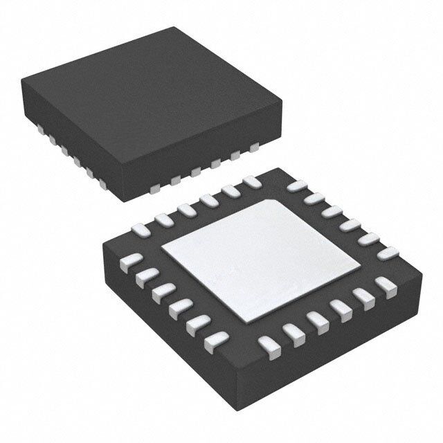
ICGOO电子元器件商城为您提供HMC533LP4E由Hittite设计生产,在icgoo商城现货销售,并且可以通过原厂、代理商等渠道进行代购。 HMC533LP4E价格参考。HittiteHMC533LP4E封装/规格:RF 其它 IC 和模块, RF IC VCO General Purpose 23.8GHz ~ 24.8GHz Dual Outputs (Divide by 16, Standard) 24-QFN (4x4)。您可以下载HMC533LP4E参考资料、Datasheet数据手册功能说明书,资料中有HMC533LP4E 详细功能的应用电路图电压和使用方法及教程。
HMC533LP4E 是 Analog Devices Inc. 生产的一款 RF(射频)IC,属于 RF 其他 IC 和模块类别。该器件是一款低噪声、宽带放大器,工作频率范围为 DC 至 18 GHz,适用于多种高频射频应用领域。以下是其主要应用场景:

1. 通信系统:
   HMC533LP4E 的宽频带特性使其非常适合用于现代通信系统中的信号放大。例如,在无线基础设施中,可用于基站、中继站和微波链路的前端或中端信号增强。

2. 测试与测量设备:
   高性能测试仪器(如频谱分析仪、网络分析仪等)需要稳定的低噪声放大器来确保高精度测量。HMC533LP4E 可用作这些设备中的前置放大器,以提高灵敏度和动态范围。

3. 雷达系统:
   在雷达应用中,这款放大器可以用来增强接收机的信号强度,同时保持较低的噪声水平,从而提升目标检测能力。它适用于军事、气象和交通监控等领域的雷达系统。

4. 卫星通信:
   卫星通信系统要求高度可靠的射频组件,HMC533LP4E 的宽带设计能够满足 Ku 波段及更高频率的应用需求,支持地面站和卫星之间的数据传输。

5. 光学模块驱动:
   在高速光通信领域,此放大器可以用作光电转换模块中的驱动电路,帮助实现更远距离的数据传输和更高的速率。

6. 航空航天与国防:
   因为其卓越的电气特性和环境适应能力,HMC533LP4E 广泛应用于航空航天和国防项目中的电子战系统、导航设备以及空间探测任务。

总结来说,HMC533LP4E 凭借其优异的性能参数(包括低噪声系数、高增益和宽带操作能力),成为众多射频相关应用的理想选择。
| 参数 | 数值 |
| 产品目录 | |
| 描述 | IC MMIC AMP VCO HBT GAAS 24-QFN |
| 产品分类 | |
| 品牌 | Hittite Microwave Corporation |
| 数据手册 | |
| 产品图片 |
|
| 产品型号 | HMC533LP4E |
| RF类型 | 通用 |
| rohs | 无铅 / 符合限制有害物质指令(RoHS)规范要求 |
| 产品系列 | - |
| 供应商器件封装 | 24-QFN(4x4) |
| 其它名称 | 1127-1450 |
| 功能 | VCO |
| 包装 | 剪带 |
| 封装/外壳 | 24-VFQFN 裸露焊盘 |
| 标准包装 | 50 |
| 辅助属性 | 双输出(除以 16,标准) |
| 频率 | 23.8GHz ~ 24.8GHz |


- 商务部:美国ITC正式对集成电路等产品启动337调查
- 曝三星4nm工艺存在良率问题 高通将骁龙8 Gen1或转产台积电
- 太阳诱电将投资9.5亿元在常州建新厂生产MLCC 预计2023年完工
- 英特尔发布欧洲新工厂建设计划 深化IDM 2.0 战略
- 台积电先进制程称霸业界 有大客户加持明年业绩稳了
- 达到5530亿美元!SIA预计今年全球半导体销售额将创下新高
- 英特尔拟将自动驾驶子公司Mobileye上市 估值或超500亿美元
- 三星加码芯片和SET,合并消费电子和移动部门,撤换高东真等 CEO
- 三星电子宣布重大人事变动 还合并消费电子和移动部门
- 海关总署:前11个月进口集成电路产品价值2.52万亿元 增长14.8%


PDF Datasheet 数据手册内容提取
HMC533LP4 533LP4E / v00.0405 MMIC VCO w/ DIVIDE-BY-16, 23.8 - 24.8 GHz Typical Applications Features Low noise MMIC VCO w/Divide-by-16 for: Pout: +12 dBm • VSAT Radio Phase Noise: -95 dBc/Hz @100 KHz Typ. • Point to Point/Multipoint Radio No External Resonator Needed • Test Equipment & Industrial Controls Single Supply: +5V @ 220 mA • Military End-Use 24 Lead 4x4mm QFN Package: 9 mm2 • Automotive Radar Functional Diagram General Description The HMC533LP4 & HMC533LP4E are GaAs InGaP Heterojunction Bipolar Transistor (HBT) MMIC VCOs. The HMC533LP4 & HMC533LP4E integrate resona- 12 tors, negative resistance devices, varactor diodes and feature a divide-by-16 output. T he VCO’s phase noise performance is excellent over temperature, shock, and T process due to the oscillator’s monolithic structure. M Power output is +12 dBm typical from a +5V supply S voltage. Prescaler function can be disabled to con- serve current if not required. The voltage controlled - oscillator is packaged in a leadless QFN 4 x 4 mm S O surface mount package. C V Electrical Specifi cations, T = +25° C, Vcc1, Vcc2, Vcc3 = +5V A Parameter Min. Typ. Max. Units Frequency Range 23.8 - 24.8 GHz Power Output RFOUT +9 +12 +15 dBm RFOUT/16 -7 -4 -1 dBm SSB Phase Noise @ 100 kHz Offset, Vtune= +5V @ RFOUT -95 dBc/Hz Tune Voltage Vtune 2 13 V Supply Current Icc 180 220 260 mA Tune Port Leakage Current (Vtune= 13V) 10 μA Output Return Loss 3 dB Harmonics/Subharmonics 1/2 26 dBc 3/2 37 dBc Pulling (into a 2.0:1 VSWR) 13 MHz pp Pushing @ Vtune= 5V 80 MHz/V Frequency Drift Rate 2.3 MHz/°C Information furnisheFd obry Apnrailcoge D, edviceelsi vise breylie,v eadn tdo bteo a cpcluaractee a nod rrdelieabrlse., Hpowleevaers, eno coFnotra pcritc eH, idtteiltieve rMy, iacnrdo wtoa pvlaec eC oorrdperosr: aAtnioalnog: Devices, Inc., responsibility is assumed by Analog Devices for its use, nor for any infringements of patents or other One Technology Way, P.O. Box 9106, Norwood, MA 02062-9106 12 - 150 rights of third parties tha2t 0ma yA relpsuhlt faro mR itos uasde. ,S pCechifiecaltmionss fsoubrjedct, toM chAan g0e1 w8ith2ou4t nPotihceo. Nnoe : P9h7o8n-e2: 75801--332394-437 0 0F (cid:127)a Ox:r d9e7r o8n-l2in5e 0at- w33w7w3.analog.com license is granted by implication or otherwise under any patent or patent rights of Analog Devices. Trademarks and registered trademarks are the property of their resOpercdtivee orw Onerns.-line at www.hAiptptilticea.tcioonm Support: Phone: 1-800-ANALOG-D
HMC533LP4 / 533LP4E v00.0405 MMIC VCO w/ DIVIDE-BY-16, 23.8 - 24.8 GHz Frequency vs. Tuning Voltage, T= 25°C Frequency vs. Tuning Voltage, Vcc= +5V 26 26 25.5 25.5 z) z) H H G 25 G 25 Y ( Y ( NC 24.5 NC 24.5 E E U U Q 24 Q 24 E E R R T F 23.5 Vcc=4.75V T F 23.5 +25 C UTPU 23 VVcccc==55..205VV UTPU 23 +-4805 CC O O 22.5 22.5 22 22 0 1 2 3 4 5 6 7 8 9 10 11 12 13 0 1 2 3 4 5 6 7 8 9 10 11 12 13 TUNING VOLTAGE (VOLTS) TUNING VOLTAGE (VOLTS) Output Power 12 Sensitivity vs. Tuning Voltage, Vcc= +5V vs. Tuning Voltage, Vcc= +5V 600 15 LT) 500 m) 12 T Y (MHz/VO 340000 ++-428055 CCC OWER (dB 9 SM NSITIVIT 200 UTPUT P 6 ++-428055 CCC S - SE O 3 O 100 C 0 0 V 0 1 2 3 4 5 6 7 8 9 10 11 12 13 0 1 2 3 4 5 6 7 8 9 10 11 12 13 TUNING VOLTAGE (VOLTS) TUNING VOLTAGE (VOLTS) Information furnisheFd obry Apnrailcoge D, edviceelsi vise breylie,v eadn tdo bteo a cpcluaractee a nod rrdelieabrlse., Hpowleevaers, eno coFnotra pcritc eH, idtteiltieve rMy, iacnrdo wtoa pvlaec eC oorrdperosr: aAtnioalnog: Devices, Inc., responsibility is assumed by Analog Devices for its use, nor for any infringements of patents or other One Technology Way, P.O. Box 9106, Norwood, MA 02062-9106 rights of third parties tha2t 0ma yA relpsuhlt faro mR itos uasde. ,S pCechifiecaltmionss fsoubrjedct, toM chAan g0e1 w8ith2ou4t nPotihceo. Nnoe : P9h7o8n-e2: 75801--332394-437 0 0F (cid:127)a Ox:r d9e7r o8n-l2in5e 0at- w33w7w3.analog.com 12 - 151 license is granted by implication or otherwise under any patent or patent rights of Analog Devices. Trademarks and registered trademarks are the property of their resOpercdtivee orw Onerns.-line at www.hAiptptilticea.tcioonm Support: Phone: 1-800-ANALOG-D
HMC533LP4 / 533LP4E v00.0405 MMIC VCO w/ DIVIDE-BY-16, 23.8 - 24.8 GHz SSB Phase Noise vs. Tuning Voltage SSB Phase Noise @ Vtune= +5V -60 0 -65 -20 Hz) -70 Hz) ++2855 CC c/ c/ -40 -40 C dB -75 dB NOISE ( --8850 11000kkHHzz o offfsfseett NOISE ( --8600 E E AS -90 AS-100 H H P -95 P B B -120 S-100 S S S -140 -105 -110 -160 1 2 3 4 5 6 7 8 9 10 11 12 13 103 104 105 106 107 TUNING VOLTAGE (VOLTS) OFFSET FREQUENCY (Hz) Divide-by-16 Frequency Divide-by-16 Output 12 vs. Tuning Voltage, Vcc= +5V Power vs. Tuning Voltage, Vcc= +5V 1.625 0 T GHz) 1.562 m) -2 M Y ( dB NC R ( -4 S UE WE Q 1.5 O E P OS - UTPUT FR 1.437 ++-428055 CCC OUTPUT --86 ++-428055 CCC O C V 1.375 -10 0 1 2 3 4 5 6 7 8 9 10 11 12 13 0 1 2 3 4 5 6 7 8 9 10 11 12 13 TUNING VOLTAGE (VOLTS) TUNING VOLTAGE (VOLTS) Absolute Maximum Ratings Typical Supply Current vs. Vcc Vcc1, Vcc2 5.5 V Vcc (V) Icc (mA) Vtune 0 to 15V Max. 4.75 200 Junction Temperature 135 °C 5.0 220 Continuous Pdiss (T=85 °C) 5.25 240 1.4 W (derate 28 mW/C above 85 °C Note: VCO will operate over full voltage range shown above. Thermal Resistance 36 °C/W Storage Temperature -65 to +150 °C Operating Temperature -40 to +85 °C ELECTROSTATIC SENSITIVE DEVICE ESD Sensitivity (HBM) Class 1A OBSERVE HANDLING PRECAUTIONS Information furnisheFd obry Apnrailcoge D, edviceelsi vise breylie,v eadn tdo bteo a cpcluaractee a nod rrdelieabrlse., Hpowleevaers, eno coFnotra pcritc eH, idtteiltieve rMy, iacnrdo wtoa pvlaec eC oorrdperosr: aAtnioalnog: Devices, Inc., responsibility is assumed by Analog Devices for its use, nor for any infringements of patents or other One Technology Way, P.O. Box 9106, Norwood, MA 02062-9106 12 - 152 rights of third parties tha2t 0ma yA relpsuhlt faro mR itos uasde. ,S pCechifiecaltmionss fsoubrjedct, toM chAan g0e1 w8ith2ou4t nPotihceo. Nnoe : P9h7o8n-e2: 75801--332394-437 0 0F (cid:127)a Ox:r d9e7r o8n-l2in5e 0at- w33w7w3.analog.com license is granted by implication or otherwise under any patent or patent rights of Analog Devices. Trademarks and registered trademarks are the property of their resOpercdtivee orw Onerns.-line at www.hAiptptilticea.tcioonm Support: Phone: 1-800-ANALOG-D
HMC533LP4 / 533LP4E v00.0405 MMIC VCO w/ DIVIDE-BY-16, 23.8 - 24.8 GHz Outline Drawing 12 NOTES: 11. LEADFRAME MATERIAL: COPPER ALLOY 2. DIMENSIONS ARE IN INCHES [MILLIMETERS] 3. LEAD SPACING TOLERANCE IS NON-CUMULATIVE. 4. PAD BURR LENGTH SHALL BE 0.15mm MAXIMUM. T PAD BURR HEIGHT SHALL BE 0.05mm MAXIMUM. M 5. PACKAGE WARP SHALL NOT EXCEED 0.05mm. 6. ALL GROUND LEADS AND GROUND PADDLE MUST BE S SOLDERED TO PCB RF GROUND. 7. REFER TO HITTITE APPLICATION NOTE FOR SUGGESTED LAND PATTERN. - Package Information S O Part Number Package Body Material Lead Finish MSL Rating Package Marking [3] C HMC533LP4 Low Stress Injection Molded Plastic Sn/Pb Solder MSL1 [1] H533 V XXXX HMC533LP4E RoHS-compliant Low Stress Injection Molded Plastic 100% matte Sn MSL1 [2] H533 XXXX [1] Max peak refl ow temperature of 235 °C [2] Max peak refl ow temperature of 260 °C [3] 4-Digit lot number XXXX Pin Descriptions Pin Number Function Description Interface Schematic 1, 15, 17, Package bottom has an exposed metal paddle that GND 21, 23 must also be connected to RF/DC ground. 2 RFOUT/16 Divided-by-16 Output Information furnisheFd obry Apnrailcoge D, edviceelsi vise breylie,v eadn tdo bteo a cpcluaractee a nod rrdelieabrlse., Hpowleevaers, eno coFnotra pcritc eH, idtteiltieve rMy, iacnrdo wtoa pvlaec eC oorrdperosr: aAtnioalnog: Devices, Inc., responsibility is assumed by Analog Devices for its use, nor for any infringements of patents or other One Technology Way, P.O. Box 9106, Norwood, MA 02062-9106 rights of third parties tha2t 0ma yA relpsuhlt faro mR itos uasde. ,S pCechifiecaltmionss fsoubrjedct, toM chAan g0e1 w8ith2ou4t nPotihceo. Nnoe : P9h7o8n-e2: 75801--332394-437 0 0F (cid:127)a Ox:r d9e7r o8n-l2in5e 0at- w33w7w3.analog.com 12 - 153 license is granted by implication or otherwise under any patent or patent rights of Analog Devices. Trademarks and registered trademarks are the property of their resOpercdtivee orw Onerns.-line at www.hAiptptilticea.tcioonm Support: Phone: 1-800-ANALOG-D
HMC533LP4 / 533LP4E v00.0405 MMIC VCO w/ DIVIDE-BY-16, 23.8 - 24.8 GHz Pin Descriptions Pin Number Function Description Interface Schematic Supply voltage for prescaler. 3, 4 VCC2, VCC3 If prescaler is not required, these pins may be left open to conserve 100 mA of current 5-14, 18, No Connection. These pins may be connected to RF/ N/C 19, 24 DC ground. Performance will not be affected. 16 RFOUT RF output (AC coupled). 12 20 VCC1 Supply Voltage, +5V T M S Control Voltage Input. Modulation port bandwidth 22 VTUNE dependent on drive source impedance. - S O C Typical Application Circuit V Information furnisheFd obry Apnrailcoge D, edviceelsi vise breylie,v eadn tdo bteo a cpcluaractee a nod rrdelieabrlse., Hpowleevaers, eno coFnotra pcritc eH, idtteiltieve rMy, iacnrdo wtoa pvlaec eC oorrdperosr: aAtnioalnog: Devices, Inc., responsibility is assumed by Analog Devices for its use, nor for any infringements of patents or other One Technology Way, P.O. Box 9106, Norwood, MA 02062-9106 12 - 154 rights of third parties tha2t 0ma yA relpsuhlt faro mR itos uasde. ,S pCechifiecaltmionss fsoubrjedct, toM chAan g0e1 w8ith2ou4t nPotihceo. Nnoe : P9h7o8n-e2: 75801--332394-437 0 0F (cid:127)a Ox:r d9e7r o8n-l2in5e 0at- w33w7w3.analog.com license is granted by implication or otherwise under any patent or patent rights of Analog Devices. Trademarks and registered trademarks are the property of their resOpercdtivee orw Onerns.-line at www.hAiptptilticea.tcioonm Support: Phone: 1-800-ANALOG-D
HMC533LP4 / 533LP4E v00.0405 MMIC VCO w/ DIVIDE-BY-16, 23.8 - 24.8 GHz Evaluation PCB 12 T M S - S O C V List of Materials for Evaluation PCB 106651 [1] The circuit board used in the fi nal application should Item Description use RF circuit design techniques. Signal lines J1 - J2 PCB Mount SMA RF Connector should have 50 ohm impedance while the package J3 2.92 mm PCB mount k-connector ground leads and backside ground slug should be J4 - J5 2 mm DC Header connected directly to the ground plane similar to that C1 - C2 4.7 μF Tantalum Capacitor shown. A sufficient number of via holes should be C3 100 pF Capacitor, 0402 Pkg. used to connect the top and bottom ground planes. C4 -C5 1,000 pF Capacitor, 0603 Pkg. The evaluation circuit board shown is available from U1 HMC533LP4 / HMC533LP4E VCO Hittite upon request. PCB [2] 106546 Eval Board [1] Reference this number when ordering complete evaluation PCB [2] Circuit Board Material: Rogers 4350 Information furnisheFd obry Apnrailcoge D, edviceelsi vise breylie,v eadn tdo bteo a cpcluaractee a nod rrdelieabrlse., Hpowleevaers, eno coFnotra pcritc eH, idtteiltieve rMy, iacnrdo wtoa pvlaec eC oorrdperosr: aAtnioalnog: Devices, Inc., responsibility is assumed by Analog Devices for its use, nor for any infringements of patents or other One Technology Way, P.O. Box 9106, Norwood, MA 02062-9106 rights of third parties tha2t 0ma yA relpsuhlt faro mR itos uasde. ,S pCechifiecaltmionss fsoubrjedct, toM chAan g0e1 w8ith2ou4t nPotihceo. Nnoe : P9h7o8n-e2: 75801--332394-437 0 0F (cid:127)a Ox:r d9e7r o8n-l2in5e 0at- w33w7w3.analog.com 12 - 155 license is granted by implication or otherwise under any patent or patent rights of Analog Devices. Trademarks and registered trademarks are the property of their resOpercdtivee orw Onerns.-line at www.hAiptptilticea.tcioonm Support: Phone: 1-800-ANALOG-D