首页 > HMC905LP3E > 详情
 Datasheet下载
- 型号: HMC905LP3E
- 制造商: Hittite
- 库位|库存: xxxx|xxxx
- 要求:
| 数量阶梯 | 香港交货 | 国内含税 |
| +xxxx | $xxxx | ¥xxxx |
查看当月历史价格
查看今年历史价格
产品参数
| 参数 | 数值 |
| 产品目录 | 射频/IF 和 RFID |
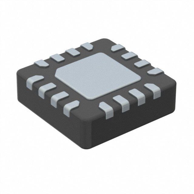
| 描述 | IC DIVIDER BICMOS SIGE LN 16-QFN |
| 产品分类 | RF 功率分配器/分线器 |
| 品牌 | Hittite Microwave Corporation |
| 数据手册 | 点击此处下载产品Datasheet |
| 产品图片 |  |
| 产品型号 | HMC905LP3E |
| rohs | 无铅 / 符合限制有害物质指令(RoHS)规范要求 |
| 产品系列 | - |
| 其它名称 | 1127-1609 1127-1609-1 1127-1609-ND |
| 包装 | 剪切带 (CT) |
| 大小/尺寸 | 3.00mm 长 x 3.00mm 宽 |
| 封装/外壳 | 16-VFQFN 裸露焊盘 |
| 插入损耗 | - |
| 标准包装 | 1 |
| 规格 | - |
| 频率 | 400MHz ~ 6GHz |
Datasheet
PDF Datasheet 数据手册内容提取
HMC905LP3E v01.0414 6 GHz LOW NOISE PROGRAMMABLE DIVIDER (N = 1 to 4) Typical Applications Features 4 4 The HMC905LP3E is ideal for: Low Noise Floor: -164 dBc/Hz at 10 MHz Offset for N = 4 • LO Generation with Low Noise Floor Programmable Frequency Divider, N = 1, 2, 3 or 4 • Software Defined Radios T T 400 MHz to 6 GHz Input Frequency Range M • Clock Generators M Up to +6 dBm Output Power S • Fast Switching Synthesizers S Sleep Mode: Consumes <1 µA - • Military Applications - S 16 Lead 3X3 mm SMT Package: 9mm2 S • Test Equipment R R • Sensors O O T T Functional Diagram General Description C C E The HMC905LP3E is a SiGe BiCMOS low noise E T programmable frequency divider in a 3x3 mm lead- T E less surface mount package. The circuit can be pro- E D grammed to divide from N = 1 to N = 4 in the 400 MHz D to 6 GHz input frequency range. The high level out- & & put power (up to 6 dBm single ended) with a very low S SSB phase noise and 50% duty cycle makes this S R device ideal for low noise clock generation, LO R E generation and LO drive applications. Configurable E D bias and output power controls allow current D I consumption and output power control. The device I V V incorporates a power down feature, good input I I D to output isolation and fast start up time. The D HMC905LP3E can be included into fast switching Y Y C “ping-pong” applications. C N N E E Electrical Specifications, T = +25° C, Vcc = +3.3V, Z = 50Ω U o U A Q Q Parameter Conditions Min. Typ. Max. Units E E RF Input Characteristics R R RF Input Frequency Single-ended input 400 6000[1] MHz F F RF Input Power Single-ended input 0 6 10 dBm Divider Output Characteristics -Typically, 50 ohms load resistors connected to Vcc Output Power (Single-ended Out) -2 3 6 dBm - 1 bit programmable (CTRL digital signal) [2] SSB Phase Noise @ 10 kHz Offset -150 dBc/Hz +6 dBm Input Power, 6 GHz input, SSB Phase Noise @ 100 kHz Offset -158 dBc/Hz Single-Ended Input and Output, Divide-by-4 [3] SSB Phase Noise @ 10 MHz Offset -164 dBc/Hz Start Up Time EN bit from OFF to ON State (0V to Vcc) 200 ns Power Down Time EN bit from ON to OFF State (Vcc to 0V) 20 ns Delay from divide ratio change Setting Time at Division Ratio Change 25 ns to output frequency change [1] Maximum 5500 MHz in Divide by 2. [2] See typical supply currents vs. BIAS0, BIAS1, CTRL bits table [3] See Residual Phase Noise plot InforFmaotiro np fruircniseh,e dd beyl iAvnealroyg Daenvidce st ois pbelaliecveed otor dbee arcsc:u rHateit taintde reMliaibcler. oHwowaevveer, Cnoo rpFoorr aptriiocen,, d2e0liv Aerlyp, haand R too apdla,c Ce horedlemrss: fAonrdal,o gM DAe v0ic1e8s2, 4Inc., responsibility is assumed by Analog Devices for its use, nor for any infringements of patents or other One Technology Way, P.O. Box 9106, Norwood, MA 02062-9106 4 - 1 rliicgehntss eo fi sth girrda nptaerdti ebsy t himatp mlicaaPyt iorhenso uonlrt ofertoh:m e9r wit7sis 8ues -eu2.n dS5ep0re ca-inf3iyc 3aptia4otne3sn ts ou rb jpeFacttae tnoxt c:r hig9ahn7tgs 8eo wf- 2Aithn5oau0lot g-n 3oDti3ecve7i.c 3eNso . POhrodnee:r 7 O81n-3-2li9n-e4 7a0t0 w(cid:127) wOrwde.hr oitntliitnee. cato wmww.analog.com Trademarks and registered trademarks arAe tphep plriocpearttyi oof nth eSir urepsppecotivret :o wPnehrso.ne: 978-250-3A3p4p3li c aotrio na Spuppsp@orht: iPtthitoen.ec: o1-m800-ANALOG-D
HMC905LP3E v01.0414 6 GHz LOW NOISE PROGRAMMABLE DIVIDER (N = 1 to 4) Electrical Specifications, T = +25° C, Vcc = +3.3V, Zo = 50Ω (Continued) A 4 4 Parameter Conditions Min. Typ. Max. Units Isolation SE Input to SE Output EN bit OFF -80 -30 dBc Duty Cycle for Differential Mode 50 % T Logic Inputs T M VIH Input High Voltage 1.5 3.3 V M S VIL Input Low Voltage 0 0.8 V S Power Supplies - - S Analog Supply S Vcc (Low Noise LDO for good phase noise - 3.15 3.3 3.45 V R R HMC860LP3E) O Current Consumption Total current vs. BIAS and CTRL bits [1] 82 100 125 mA O T T Sleep Current EN = 0V 1 µA C C [1] The bias bits combination BIAS1 BIAS0 = 1 1 is not recommended E E T T All data plots taken on Evaluation Board (schematic on page 10) single-ended with the unused E E output port 50 ohms terminated, Vcc = +3.3V, Ta=+25 °C, except stated otherwise D D & Residual Phase Noise & Input Sensitivity Window Divide by 1, 2, 3 & 4 [2] S S R 10 -110 R E E D m) 5 O Rpeecraotminmg eWnidneddo w c/Hz)-120 DDiivv BByy 12 D VI R (dB 0 E (dB-130 DDiivv BByy 34 VI E S DI OW -5 NOI-140 DI T P SE Y PU -10 HA-150 Y N P C I BIAS1BIAS0=01 B C N -15 BBIIAASS11BBIIAASS00==0100 SS-160 N E Operating Window E -20 -170 U 0 1 2 3 4 5 6 7 10 100 1000 104 105 106 107 108 U INPUT FREQUENCY (GHz) OFFSET FREQUENCY (Hz) Q Q E Phase Noise for 3 Cascaded Output Phase Noise vs. Input Power E R R HMC905LP3E from 6 GHz VCO Divide-by-4 F F -10 -90 -30 -100 Hz) -50 VCO IN Hz)-110 E (dBc/ -70 DDDiiivvv BBByyy 41664 E (dBc/-120 S S OI -90 OI-130 N N SE -110 SE -140 Source IN HA HA Div By 4 0dBm P-130 P-150 Div By 4 3dBm B B Div By 4 6dBm S S S-150 S-160 Div By 4 9dBm -170 -170 10 100 1000 104 105 106 107 1000 104 105 106 107 OFFSET FREQUENCY (Hz) OFFSET FREQUENCY (Hz) [2] Fin = 6 GHz, Pin = 6 dBm, CTRL = 1, BIAS1 BIAS0 = 01 InforFmaotiro np fruircniseh,e dd beyl iAvnealroyg Daenvidce st ois pbelaliecveed otor dbee arcsc:u rHateit taintde reMliaibcler. oHwowaevveer, Cnoo rpFoorr aptriiocen,, d2e0liv Aerlyp, haand R too apdla,c Ce horedlemrss: fAonrdal,o gM DAe v0ic1e8s2, 4Inc., responsibility is assumed by Analog Devices for its use, nor for any infringements of patents or other One Technology Way, P.O. Box 9106, Norwood, MA 02062-9106 rights of third parties that maPy rhesounlt fero:m 9 it7s 8us-e2. S5p0ec-if3ic3ati4on3s s u b jeFcta tox c: h9an7g8e w-2ith5ou0t -n3oti3ce7. 3No POhrodnee:r 7 O81n-3-2li9n-e4 7a0t0 w(cid:127) wOrwde.hr oitntliitnee. cato wmww.analog.com 4 - 2 license is granted by implication or otherwise under any patent or patent rights of Analog Devices. Trademarks and registered trademarks arAe tphep plriocpearttyi oof nth eSir urepsppecotivret :o wPnehrso.ne: 978-250-3A3p4p3li c aotrio na Spuppsp@orht: iPtthitoen.ec: o1-m800-ANALOG-D
HMC905LP3E v01.0414 6 GHz LOW NOISE PROGRAMMABLE DIVIDER (N = 1 to 4) Output Power vs. Temperature Pout vs. Division Ratio Divide-by-4 4 4 10 10 CTRL=1, BIAS1BIAS0=01 CTRL=1, BIAS1BIAS0=01->101 CTRL=0, BIAS1BIAS0=00->000 Bm) 5 Bm) 5 T R (d R (d T E E M W W M O 0 O 0 P P S UT UT +25°C 101 S S - OUTP -5 DDDiiivvv bbbyyy 432 OUTP -5 + +-824550°°°CCC 101000101 S - Div by 1 +85°C 000 R -40°C 000 R O -100 1 2 3 4 5 6 7 8 -100 1 2 3 4 5 6 7 8 O T INPUT FREQUENCY (GHz) INPUT FREQUENCY (GHz) T C C E E T Output Power vs. Input Power Level T E Divide-by-4 Pout Divide-by-4 vs. CTRL & BIAS E D D 10 10 CTRL=1, BIAS1BIAS0=01 & & m) m) S B 5 B 5 S d d R R ( R ( R E E E W W E O 0 O 0 D T P T P D U U I P P CTRL=0, BIAS=00 I IV OUT -5 63ddBBmm OUT -5 CCTTRRLL==10,,BBIIAASS==0001 IV D 9dBm CTRL=1,BIAS=01 D Y -10 -10 Y 0 1 2 3 4 5 6 7 8 0 1 2 3 4 5 6 7 8 C C INPUT FREQUENCY (GHz) INPUT FREQUENCY (GHz) N N E E U Output Power vs. Voltage Supply U Q Q Divide-by-4 E E 10 R CTRL=1, BIAS1BIAS0=01 R F F m) B 5 d R ( E W O 0 P T U P UT 3.3V O -5 3.15V 3.45V -10 0 1 2 3 4 5 6 7 8 INPUT FREQUENCY (GHz) [1] CTRL = 0, BIAS1, BIAS1 BIAS0 = 00, Pin = 6 dBm InforFmaotiro np fruircniseh,e dd beyl iAvnealroyg Daenvidce st ois pbelaliecveed otor dbee arcsc:u rHateit taintde reMliaibcler. oHwowaevveer, Cnoo rpFoorr aptriiocen,, d2e0liv Aerlyp, haand R too apdla,c Ce horedlemrss: fAonrdal,o gM DAe v0ic1e8s2, 4Inc., responsibility is assumed by Analog Devices for its use, nor for any infringements of patents or other One Technology Way, P.O. Box 9106, Norwood, MA 02062-9106 4 - 3 rliicgehntss eo fi sth girrda nptaerdti ebsy t himatp mlicaaPyt iorhenso uonlrt ofertoh:m e9r wit7sis 8ues -eu2.n dS5ep0re ca-inf3iyc 3aptia4otne3sn ts ou rb jpeFacttae tnoxt c:r hig9ahn7tgs 8eo wf- 2Aithn5oau0lot g-n 3oDti3ecve7i.c 3eNso . POhrodnee:r 7 O81n-3-2li9n-e4 7a0t0 w(cid:127) wOrwde.hr oitntliitnee. cato wmww.analog.com Trademarks and registered trademarks arAe tphep plriocpearttyi oof nth eSir urepsppecotivret :o wPnehrso.ne: 978-250-3A3p4p3li c aotrio na Spuppsp@orht: iPtthitoen.ec: o1-m800-ANALOG-D
HMC905LP3E v01.0414 6 GHz LOW NOISE PROGRAMMABLE DIVIDER (N = 1 to 4) H2, H3, H4, H5 Harmonics, Divide-by-1 [1] H2, H3, H4, H5 Harmonics, Divide-by-2 [1] 4 4 0 0 CTRL=0,BIAS1BIAS0=00 H2 Bc) -10 H3 Bc) -10 d H4 d 1 ( H5 2 ( -20 T Y- Y- T B -20 B M DE- DE- -30 M VI VI S S DI -30 S DI -40 S C C - NI NI -50 H2 - S RMO -40 RMO -60 HH34 S R HA HA H5 R O -500 1 2 3 4 5 6 7 -700 1 2 3 4 5 6 7 O T INPUT FREQUENCY (GHz) INPUT FREQUENCY (GHz) T C C E E T T E H2, H3, H4, H5 Harmonics, Divide-by-3 [1] H2, H3, H4, H5 Harmonics, Divide-by-4 [1] E D D 0 0 & & Bc) -10 Bc) -10 S 3 (d -20 4 (d S R Y- Y- R B B -20 E DE- -30 DE- E D S DIVI -40 H2 S DIVI -30 D VI NIC -50 H3 NIC H2 VI DI RMO -60 HH45 RMO -40 HH34 DI HA HA H5 Y -70 -50 Y 0 1 2 3 4 5 6 7 0 1 2 3 4 5 6 7 C C INPUT FREQUENCY (GHz) INPUT FREQUENCY (GHz) N N E E U U Q Input to Output Isolation Q E E -20 R R c) B F d -30 F N ( O ATI -40 L O S T I -50 U P T U -60 O T U P -70 N I -80 0 1 2 3 4 5 6 7 INPUT FREQUENCY (GHz) [1] CTRL = 0, BIAS1, BIAS1 BIAS0 = 00, Pin = 6 dBm InforFmaotiro np fruircniseh,e dd beyl iAvnealroyg Daenvidce st ois pbelaliecveed otor dbee arcsc:u rHateit taintde reMliaibcler. oHwowaevveer, Cnoo rpFoorr aptriiocen,, d2e0liv Aerlyp, haand R too apdla,c Ce horedlemrss: fAonrdal,o gM DAe v0ic1e8s2, 4Inc., responsibility is assumed by Analog Devices for its use, nor for any infringements of patents or other One Technology Way, P.O. Box 9106, Norwood, MA 02062-9106 rights of third parties that maPy rhesounlt fero:m 9 it7s 8us-e2. S5p0ec-if3ic3ati4on3s s u b jeFcta tox c: h9an7g8e w-2ith5ou0t -n3oti3ce7. 3No POhrodnee:r 7 O81n-3-2li9n-e4 7a0t0 w(cid:127) wOrwde.hr oitntliitnee. cato wmww.analog.com 4 - 4 license is granted by implication or otherwise under any patent or patent rights of Analog Devices. Trademarks and registered trademarks arAe tphep plriocpearttyi oof nth eSir urepsppecotivret :o wPnehrso.ne: 978-250-3A3p4p3li c aotrio na Spuppsp@orht: iPtthitoen.ec: o1-m800-ANALOG-D
HMC905LP3E v01.0414 6 GHz LOW NOISE PROGRAMMABLE DIVIDER (N = 1 to 4) Programming Truth Table Absolute Maximum Ratings for Frequency Division Ratios 4 4 RF Input Power 12 dBm B1 B0 Divide-by Supply Voltage (Vcc) 3.6V 0 0 1 Control Inputs 0 1 2 3.6V (B0, B1, CTRL, Bias0, EN) T 1 0 3 T Junction Temperature 125 °C M 1 1 4 M Continuous Pdiss (T = 85 °C) S 1.3 W 0 = Logic Low S (derate 33 mW/ °C above 85 °C) 1 = Logic High - Thermal Resistance - S (Junction to ground paddle) 30 °C/W Digital Control Input Voltages S R Storage Temperature -65 to +125 °C R O Operating Temperature -40 to +85 °C State B0, B1, CTRL, BIAS1, BIAS0, EN O T ESD Sensitivity (HBM) Class 1A Low 0 to 0.8V T C High 1.5V to 3.3V C E E ELECTROSTATIC SENSITIVE DEVICE T T OBSERVE HANDLING PRECAUTIONS E E D D & Typical Supply Current vs. EN, BIAS0, BIAS1 & CTRL Bits & S S 3.3V Supply Typ. Pout Typ. R EN CTRL BIAS1 BIAS0 Noise Floor R Current (mA) (dBm) E E 1 0 0 0 84 1.5 Low D D 1 0 0 1 105 4.8 I I V 1 0 1 0 98 3.9 V DI 1 1 0 0 100 2.4 Better DI 1 1 0 1 120 6.3 Best Y Y 1 1 1 0 113 5.3 C C 0 x x x 0.001 -55 N N Note: Currents for the divide-by-4 option, 2 GHz and 6 dBm input and 3.3V; for Vcc voltage supply from E E 3.15V to 3.45V, the HMC905LP3E total current is varying with a maximum of ~8% around typical values. U With temperature, the total current is changing from +25°C to -40°C/+85°C with about ±3%. U Q Q E E R R F F InforFmaotiro np fruircniseh,e dd beyl iAvnealroyg Daenvidce st ois pbelaliecveed otor dbee arcsc:u rHateit taintde reMliaibcler. oHwowaevveer, Cnoo rpFoorr aptriiocen,, d2e0liv Aerlyp, haand R too apdla,c Ce horedlemrss: fAonrdal,o gM DAe v0ic1e8s2, 4Inc., responsibility is assumed by Analog Devices for its use, nor for any infringements of patents or other One Technology Way, P.O. Box 9106, Norwood, MA 02062-9106 4 - 5 rliicgehntss eo fi sth girrda nptaerdti ebsy t himatp mlicaaPyt iorhenso uonlrt ofertoh:m e9r wit7sis 8ues -eu2.n dS5ep0re ca-inf3iyc 3aptia4otne3sn ts ou rb jpeFacttae tnoxt c:r hig9ahn7tgs 8eo wf- 2Aithn5oau0lot g-n 3oDti3ecve7i.c 3eNso . POhrodnee:r 7 O81n-3-2li9n-e4 7a0t0 w(cid:127) wOrwde.hr oitntliitnee. cato wmww.analog.com Trademarks and registered trademarks arAe tphep plriocpearttyi oof nth eSir urepsppecotivret :o wPnehrso.ne: 978-250-3A3p4p3li c aotrio na Spuppsp@orht: iPtthitoen.ec: o1-m800-ANALOG-D
HMC905LP3E v01.0414 6 GHz LOW NOISE PROGRAMMABLE DIVIDER (N = 1 to 4) Outline Drawing 4 4 T T M M S S - - S S R R O O T T C C E E T T E E D NOTES: D 1. LEADFRAME MATERIAL: COPPER ALLOY & & 2. DIMENSIONS ARE IN INCHES [MILLIMETERS]. 3. LEAD SPACING TOLERANCE IS NON-CUMULATIVE S S 4. PAD BURR LENGTH SHALL BE 0.15mm MAXIMUM. R R PAD BURR HEIGHT SHALL BE 0.05mm MAXIMUM. E 5. PACKAGE WARP SHALL NOT EXCEED 0.05mm. E D 6. ALL GROUND LEADS AND GROUND PADDLE MUST D BE SOLDERED TO PCB RF GROUND. I I V 7. REFER TO HITTITE APPLICATION NOTE FOR SUGGESTED V I Package Information PCB LAND PATTERN. I D D Y Part Number Package Body Material Lead Finish MSL Rating Package Marking [1] Y C HMC905LP3E RoHS-compliant Low Stress Injection Molded Plastic 100% matte Sn MSL1 [2] 905 C XXX N N [1] 4-Digit lot number XXXX E E [2] Max peak reflow temperature of 260 °C U U Q Q E E R R F F InforFmaotiro np fruircniseh,e dd beyl iAvnealroyg Daenvidce st ois pbelaliecveed otor dbee arcsc:u rHateit taintde reMliaibcler. oHwowaevveer, Cnoo rpFoorr aptriiocen,, d2e0liv Aerlyp, haand R too apdla,c Ce horedlemrss: fAonrdal,o gM DAe v0ic1e8s2, 4Inc., responsibility is assumed by Analog Devices for its use, nor for any infringements of patents or other One Technology Way, P.O. Box 9106, Norwood, MA 02062-9106 rights of third parties that maPy rhesounlt fero:m 9 it7s 8us-e2. S5p0ec-if3ic3ati4on3s s u b jeFcta tox c: h9an7g8e w-2ith5ou0t -n3oti3ce7. 3No POhrodnee:r 7 O81n-3-2li9n-e4 7a0t0 w(cid:127) wOrwde.hr oitntliitnee. cato wmww.analog.com 4 - 6 license is granted by implication or otherwise under any patent or patent rights of Analog Devices. Trademarks and registered trademarks arAe tphep plriocpearttyi oof nth eSir urepsppecotivret :o wPnehrso.ne: 978-250-3A3p4p3li c aotrio na Spuppsp@orht: iPtthitoen.ec: o1-m800-ANALOG-D
HMC905LP3E v01.0414 6 GHz LOW NOISE PROGRAMMABLE DIVIDER (N = 1 to 4) Pin Description 4 4 Pin Number Function Description Interface Schematic T 1 Vcc +3.3V Voltage Supply T M M S S - - S S R R O RF Positive Input. O 2 RFINP Input is DC coupled, external DC blocks required. T T C C E E T T E E D D & & S RF Negative Input. S 3 RFINN R Input is DC coupled, external DC blocks required. R E E D D I I V V I I D D 4 GND This pin must be connected to RF/DC ground. Y Y C Division ratio (LSB) C 5 B0 N See programming truth table. N E E Division ratio (MSB) 6 B1 U See programming truth table. U Q Q E 7 CTRL Divider Output Buffer Power Control E R R F 13 BIAS1 Divider Core Bias Control F 14 BIAS0 Divider Core Bias Control 15 EN Chip Enable No connection required. This pin may be 8, 9, 12, 16 N/C connected to ground, without affecting performance. InforFmaotiro np fruircniseh,e dd beyl iAvnealroyg Daenvidce st ois pbelaliecveed otor dbee arcsc:u rHateit taintde reMliaibcler. oHwowaevveer, Cnoo rpFoorr aptriiocen,, d2e0liv Aerlyp, haand R too apdla,c Ce horedlemrss: fAonrdal,o gM DAe v0ic1e8s2, 4Inc., responsibility is assumed by Analog Devices for its use, nor for any infringements of patents or other One Technology Way, P.O. Box 9106, Norwood, MA 02062-9106 4 - 7 rliicgehntss eo fi sth girrda nptaerdti ebsy t himatp mlicaaPyt iorhenso uonlrt ofertoh:m e9r wit7sis 8ues -eu2.n dS5ep0re ca-inf3iyc 3aptia4otne3sn ts ou rb jpeFacttae tnoxt c:r hig9ahn7tgs 8eo wf- 2Aithn5oau0lot g-n 3oDti3ecve7i.c 3eNso . POhrodnee:r 7 O81n-3-2li9n-e4 7a0t0 w(cid:127) wOrwde.hr oitntliitnee. cato wmww.analog.com Trademarks and registered trademarks arAe tphep plriocpearttyi oof nth eSir urepsppecotivret :o wPnehrso.ne: 978-250-3A3p4p3li c aotrio na Spuppsp@orht: iPtthitoen.ec: o1-m800-ANALOG-D
HMC905LP3E v01.0414 6 GHz LOW NOISE PROGRAMMABLE DIVIDER (N = 1 to 4) Pin Description (Continued) 4 4 Pin Number Function Description Interface Schematic T T Divider Negative Output, Open Drain. M 10 IOUTN M Typically 50 Ohms connected to Vcc. S S - - S S R R O O T 11 IOUTP Divider Positive Output, Open Drain. T Typically 50 Ohms connected to Vcc. C C E E T T E E D D & & Application Note: S S R The HMC905LP3E is a high performance RF divider. Such dividers are high gain devices with internal feedback. The R device will oscillate if used with AC coupled RF inputs and if no RF input is applied. Normally, if the RF input signal E E is removed the device should be disabled, or it should be placed in divide by 1 mode. The device is stable in divide D D by one mode with no RF input. The device will oscillate in divide 2, 3, or 4 modes with no RF input. In general, very I I V small RF input levels will stop all oscillations. At the minimum rated RF input sensitivity level or higher, no oscillations V I or spurious signals exist and excellent low noise performance is achieved. For input frequency lower than 400 MHz, I D D square wave input signal is recommended. Y For single ended applications, apply the signal on the positive input RFinp and terminate the unused output with 50 Y C ohms. C N N E E U U Q Q E E R R F F InforFmaotiro np fruircniseh,e dd beyl iAvnealroyg Daenvidce st ois pbelaliecveed otor dbee arcsc:u rHateit taintde reMliaibcler. oHwowaevveer, Cnoo rpFoorr aptriiocen,, d2e0liv Aerlyp, haand R too apdla,c Ce horedlemrss: fAonrdal,o gM DAe v0ic1e8s2, 4Inc., responsibility is assumed by Analog Devices for its use, nor for any infringements of patents or other One Technology Way, P.O. Box 9106, Norwood, MA 02062-9106 rights of third parties that maPy rhesounlt fero:m 9 it7s 8us-e2. S5p0ec-if3ic3ati4on3s s u b jeFcta tox c: h9an7g8e w-2ith5ou0t -n3oti3ce7. 3No POhrodnee:r 7 O81n-3-2li9n-e4 7a0t0 w(cid:127) wOrwde.hr oitntliitnee. cato wmww.analog.com 4 - 8 license is granted by implication or otherwise under any patent or patent rights of Analog Devices. Trademarks and registered trademarks arAe tphep plriocpearttyi oof nth eSir urepsppecotivret :o wPnehrso.ne: 978-250-3A3p4p3li c aotrio na Spuppsp@orht: iPtthitoen.ec: o1-m800-ANALOG-D
HMC905LP3E v01.0414 6 GHz LOW NOISE PROGRAMMABLE DIVIDER (N = 1 to 4) Evaluation PCB 4 4 T T M M S S - - S S R R O O T T C C E E T T E E D D & & S S R R E E D D I I V V I I D D Y Y C C N N E E U List of Materials for Evaluation PCB 126830 [1] U Q The circuit board used in the application should Q Item Description E use RF circuit design techniques. Signal lines should E J3 DC Connector R have 50 ohm impedance while the package ground R J1, J4, J7, J8 SMA SRI Connector F leads and backside ground paddle should be con- F C1, C2, C10 - C12, C18 1nF Capacitor, 0402 Pkg nected directly to the ground plane similar to that C3, C6, C9 100nF Capacitor, 0402 Pkg shown. A sufficient number of via holes should be C5 10uF Capacitor, 1206 Pkg used to connect the top and bottom ground planes. C8 10pF Capacitor, 0402 Pkg The evaluation circuit board shown is available from R1, R7 51 Ohms, Resistor, 0402 Pkg Hittite upon request. R2 - R6, R9 100 kOhms, Resistor, 0402 Pkg TP1, TP3, TP4 PC Compact SMT U1 HMC905LP3E Programmable Divider PCB [2] 126828 Eval Board [1] Reference this number when ordering complete evaluation PCB [2] Circuit Board Material: Rogers 4350 or Arlon 25FR InforFmaotiro np fruircniseh,e dd beyl iAvnealroyg Daenvidce st ois pbelaliecveed otor dbee arcsc:u rHateit taintde reMliaibcler. oHwowaevveer, Cnoo rpFoorr aptriiocen,, d2e0liv Aerlyp, haand R too apdla,c Ce horedlemrss: fAonrdal,o gM DAe v0ic1e8s2, 4Inc., responsibility is assumed by Analog Devices for its use, nor for any infringements of patents or other One Technology Way, P.O. Box 9106, Norwood, MA 02062-9106 4 - 9 rliicgehntss eo fi sth girrda nptaerdti ebsy t himatp mlicaaPyt iorhenso uonlrt ofertoh:m e9r wit7sis 8ues -eu2.n dS5ep0re ca-inf3iyc 3aptia4otne3sn ts ou rb jpeFacttae tnoxt c:r hig9ahn7tgs 8eo wf- 2Aithn5oau0lot g-n 3oDti3ecve7i.c 3eNso . POhrodnee:r 7 O81n-3-2li9n-e4 7a0t0 w(cid:127) wOrwde.hr oitntliitnee. cato wmww.analog.com Trademarks and registered trademarks arAe tphep plriocpearttyi oof nth eSir urepsppecotivret :o wPnehrso.ne: 978-250-3A3p4p3li c aotrio na Spuppsp@orht: iPtthitoen.ec: o1-m800-ANALOG-D
HMC905LP3E v01.0414 6 GHz LOW NOISE PROGRAMMABLE DIVIDER (N = 1 to 4) Evaluation PCB Schematic 4 4 T T M M S S - - S S R R O O T T C C E E T T E E D D & & S S R R E E D D I I V V I I D D Y Y C C N N E E U U Q Q E E R R F F InforFmaotiro np fruircniseh,e dd beyl iAvnealroyg Daenvidce st ois pbelaliecveed otor dbee arcsc:u rHateit taintde reMliaibcler. oHwowaevveer, Cnoo rpFoorr aptriiocen,, d2e0liv Aerlyp, haand R too apdla,c Ce horedlemrss: fAonrdal,o gM DAe v0ic1e8s2, 4Inc., responsibility is assumed by Analog Devices for its use, nor for any infringements of patents or other One Technology Way, P.O. Box 9106, Norwood, MA 02062-9106 rights of third parties that maPy rhesounlt fero:m 9 it7s 8us-e2. S5p0ec-if3ic3ati4on3s s u b jeFcta tox c: h9an7g8e w-2ith5ou0t -n3oti3ce7. 3No POhrodnee:r 7 O81n-3-2li9n-e4 7a0t0 w(cid:127) wOrwde.hr oitntliitnee. cato wmww.analog.com 4 - 10 license is granted by implication or otherwise under any patent or patent rights of Analog Devices. Trademarks and registered trademarks arAe tphep plriocpearttyi oof nth eSir urepsppecotivret :o wPnehrso.ne: 978-250-3A3p4p3li c aotrio na Spuppsp@orht: iPtthitoen.ec: o1-m800-ANALOG-D