ICGOO在线商城 > 射频/IF 和 RFID > RF 其它 IC 和模块 > MAPS-010164-TR0500
 Datasheet下载
- 型号: MAPS-010164-TR0500
- 制造商: M/A-COM
- 库位|库存: xxxx|xxxx
- 要求:
| 数量阶梯 | 香港交货 | 国内含税 |
| +xxxx | $xxxx | ¥xxxx |
查看当月历史价格
查看今年历史价格
MAPS-010164-TR0500产品简介:
ICGOO电子元器件商城为您提供MAPS-010164-TR0500由M/A-COM设计生产,在icgoo商城现货销售,并且可以通过原厂、代理商等渠道进行代购。 MAPS-010164-TR0500价格参考¥441.67-¥460.41。M/A-COMMAPS-010164-TR0500封装/规格:RF 其它 IC 和模块, RF IC Phase Shifter Radar 2.3GHz ~ 3.8GHz 24-PQFN (4x4)。您可以下载MAPS-010164-TR0500参考资料、Datasheet数据手册功能说明书,资料中有MAPS-010164-TR0500 详细功能的应用电路图电压和使用方法及教程。
M/A-Com Technology Solutions 的 MAPS-010164-TR0500 是一款高性能射频(RF)放大器模块,属于RF其它IC和模块类别。该器件主要工作在DC至6 GHz宽频范围内,具有高线性度、低噪声和优异的功率效率,适用于对信号完整性要求较高的无线通信系统。

典型应用场景包括:蜂窝基站基础设施中的前端模块,用于增强接收灵敏度和信号传输质量;微波点对点通信系统,支持高数据速率传输;宽带无线接入系统如5G小基站和固定无线接入(FWA)设备;以及测试与测量仪器,如频谱分析仪和信号发生器,用作内部增益级以提升系统动态范围。

此外,MAPS-010164-TR0500也适用于国防与航空航天领域的电子战系统、雷达前端和宽带接收机,因其具备良好的温度稳定性和可靠性,可在严苛环境中稳定工作。其紧凑的表面贴装封装(SMT)设计便于集成到高密度PCB布局中,适合小型化、高性能的现代射频模块设计。

综上,该器件广泛应用于通信基础设施、工业测试设备及高端国防电子系统中,是实现高性能射频信号放大的关键组件。
| 参数 | 数值 |
| 产品目录 | |
| 描述 | PHASE SHIFT 6-BIT 2.3-3.8 GHZ |
| 产品分类 | |
| 品牌 | M/A-Com Technology Solutions |
| 数据手册 | |
| 产品图片 |
|
| 产品型号 | MAPS-010164-TR0500 |
| RF类型 | 雷达 |
| rohs | 无铅 / 符合限制有害物质指令(RoHS)规范要求 |
| 产品系列 | - |
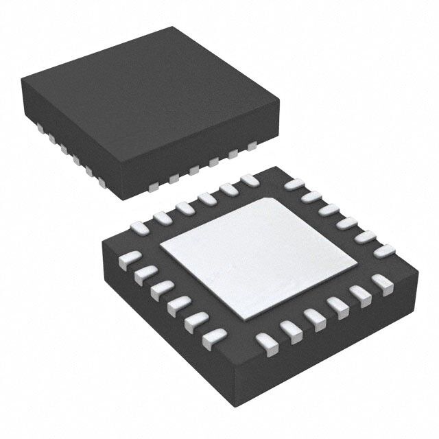
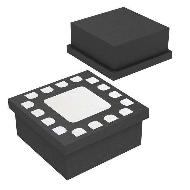
| 供应商器件封装 | 24-PQFN (4x4) |
| 其它名称 | 1465-1347-6 |
| 功能 | 相移 |
| 包装 | Digi-Reel® |
| 封装/外壳 | 24-VFQFN 裸露焊盘 |
| 标准包装 | 1 |
| 辅助属性 | - |
| 频率 | 2.3GHz ~ 3.8GHz |


- 商务部:美国ITC正式对集成电路等产品启动337调查
- 曝三星4nm工艺存在良率问题 高通将骁龙8 Gen1或转产台积电
- 太阳诱电将投资9.5亿元在常州建新厂生产MLCC 预计2023年完工
- 英特尔发布欧洲新工厂建设计划 深化IDM 2.0 战略
- 台积电先进制程称霸业界 有大客户加持明年业绩稳了
- 达到5530亿美元!SIA预计今年全球半导体销售额将创下新高
- 英特尔拟将自动驾驶子公司Mobileye上市 估值或超500亿美元
- 三星加码芯片和SET,合并消费电子和移动部门,撤换高东真等 CEO
- 三星电子宣布重大人事变动 还合并消费电子和移动部门
- 海关总署:前11个月进口集成电路产品价值2.52万亿元 增长14.8%


PDF Datasheet 数据手册内容提取
MAPS-010164 Digital Phase Shifter 6-Bit, 2.3 - 3.8 GHz Rev. V3 Features Functional Schematic 6 Bit Digital Phase Shifter 360° Coverage with LSB = 5.6° Integrated CMOS Driver Serial or Parallel Control Low DC Power Consumption Minimal Attenuation Variation over Phase Shift P/S Range 50 Ω Impedance EAR99 Lead-Free 4 mm 24-Lead PQFN Package RoHS* Compliant Description The MAPS-010164 is a GaAs pHEMT 6-bit digital phase shifter with an integrated CMOS driver in a 4 mm PQFN plastic surface mount package. Step size is 5.6° providing phase shift from 0° to 360° in 5.6° steps. This design has been optimized to minimize variation in attenuation over the phase shift Pin Configuration 2 range. Pin No. Function Pin No. Function The MAPS-010164 is ideally suited for use where high phase accuracy with minimum loss variation 1 VEE 13 GND over the phase shift range are required. The 4 mm 2 P/S 14 RF OUT PQFN package provides a smaller footprint than is typically available for a digital phase shifter with an 3 GND 15 GND internal driver. Typical applications include 4 GND 16 GND communications antennas and phased array radars. 5 RF IN 17 SER OUT 6 GND 18 VCC Ordering Information 1 7 GND 19 D6 Part Number Package 8 GND 20 D5 MAPS-010164-TR0500 500 piece reel 9 GND 21 D4 10 GND 22 D3 or LE MAPS-010164-001SMB Sample Test Board 11 GND 23 D2 or CLK 1. Reference Application Note M513 for reel size information. 12 GND 24 D1 or SER IN 2. The exposed pad centered on the package bottom must be connected to RF and DC ground. * Restrictions on Hazardous Substances, European Union Directive 2002/95/EC. 111 M/A-COM Technology Solutions Inc. (MACOM) and its affiliates reserve the right to make changes to the product(s) or information contained herein without notice. Visit www.macom.com for additional data sheets and product information. For further information and support please visit: https://www.macom.com/support
MAPS-010164 Digital Phase Shifter 6-Bit, 2.3 - 3.8 GHz Rev. V3 Electrical Specifications: Freq. = 2.3 - 3.8 GHz, T = 25°C, Z = 50 Ω, V = +5.0 V, V = -5.0 V A 0 CC EE Parameter Test Conditions Units Min. Typ. Max. Operating Power 3 2.3 - 3.8 GHz dBm — — +25 Insertion Loss Any Phase State dB — 3.2 4.5 (Any Phase State) Attenuation Variation Across All Phase States dB — ± 0.6 — All Values Relative to Insertion Loss at RMS Attenuation Error 4 dB — 0.3 — Reference Phase RMS Phase Error 4 All Values Relative to Reference Phase deg — 3 — 5.6 Degree Bit — ± 1.5 — 11.2 Degree Bit — ± 1.5 — 22.5 Degree Bit — ± 2 — Phase Accuracy 45 Degree Bit deg — ± 2 — Relative to Reference Loss State 90 Degree Bit — ± 3 — 180 Degree Bit — ± 4 — Sum of All Bits —- ± 5 — RF IN — 1.3:1 — VSWR Ratio RF OUT — 1.3:1 — 1 dB Compression Reference State dBm — 25 — Input IP3 Two-tone inputs up to +5 dBm dBm — 45 — T , T 10% to 90% RF, 90% to 10% RF ns — 50 — RISE FALL V — 3.0 — 5.5 CC V V — -5.5 -5.0 -3.0 EE V LOW-level input voltage 0.0 — 0.3 x V IL V CC V HIGH-level input voltage 0.7 x V — V IH CC CC l (Input Control Current) V = V or GND µA — 1 — IN IN CC V For serial out; I = -100 µA V - 0.2 — — OH OH V CC V For serial out; I = 100 µA — — 0.2 OL OL Icc Vcntrl = V or GND µA — — 2.5 (Quiescent Supply Current) CC V min to max I EE mA -1.0 -0.1 — EE Vin = V or V IL IH 3. Maximum operating power is the maximum power where the specifications are guaranteed. 4. RMS is calculated across all 63 amplitude or phase states relative to the amplitude or phase in the 0° phase state at a given frequency. 222 M/A-COM Technology Solutions Inc. (MACOM) and its affiliates reserve the right to make changes to the product(s) or information contained herein without notice. Visit www.macom.com for additional data sheets and product information. For further information and support please visit: https://www.macom.com/support
MAPS-010164 Digital Phase Shifter 6-Bit, 2.3 - 3.8 GHz Rev. V3 Absolute Maximum Ratings 5,6 Sample Board Header Pin Labels Parameter Absolute Maximum Input Power +27 dBm 2.3 - 3.8 GHz V -0.5V ≤ V ≤ +7.0V CC CC V -7.0V ≤ V ≤ +0.5V EE EE D1-D6, P/S, LE, CLK or -0.5V ≤ V ≤ VCC + 0.5V SER IN IN SER OUT -0.5V ≤ V ≤ V + 0.5V OUT CC Operating Temperature -40ºC to +85ºC Storage Temperature -65ºC to +150ºC 5. Exceeding any one or combination of these limits may cause permanent damage to this device. 6. M/A-COM Technology Solutions does not recommend sustained operation near these survivability limits. Handling Procedures Please observe the following precautions to avoid damage: Static Sensitivity Gallium Arsenide and Silicon Integrated Circuits are sensitive to electrostatic discharge (ESD) and can be damaged by static electricity. Proper ESD control techniques should be used when handling these devices. 333 M/A-COM Technology Solutions Inc. (MACOM) and its affiliates reserve the right to make changes to the product(s) or information contained herein without notice. Visit www.macom.com for additional data sheets and product information. For further information and support please visit: https://www.macom.com/support
MAPS-010164 Digital Phase Shifter 6-Bit, 2.3 - 3.8 GHz Rev. V3 Typical Performance Curves RF Return Loss vs. Frequency (All States) RF Return Loss vs. Frequency (All States) IN OUT -10 -10 -15 -15 -20 -20 -25 -25 -30 -30 -35 -35 -40 -40 -45 -45 -50 -50 2.2 2.4 2.6 2.8 3.0 3.2 3.4 3.6 3.8 4.0 2.2 2.4 2.6 2.8 3.0 3.2 3.4 3.6 3.8 4.0 Frequency (GHz) Frequency (GHz) Mean RMS Phase Error vs. Frequency Mean RMS Amplitude Error vs. Frequency 10 0.6 8 0.5 6 0.4 4 0.3 2 0.2 0 0.1 2.2 2.4 2.6 2.8 3.0 3.2 3.4 3.6 3.8 4.0 2.2 2.4 2.6 2.8 3.0 3.2 3.4 3.6 3.8 4.0 Frequency (GHz) Frequency (GHz) Phase Error (degrees) vs. State Amplitude Error (dB) vs. State 8 2.0 2.3 GHz 2.3 GHz 3.0 GHz 1.5 3.0 GHz 4 3.8 GHz 3.8 GHz 1.0 0.5 0 0.0 -4 -0.5 -1.0 -8 -1.5 -12 -2.0 0 45 90 135 180 225 270 315 360 0 45 90 135 180 225 270 315 360 State State 444 M/A-COM Technology Solutions Inc. (MACOM) and its affiliates reserve the right to make changes to the product(s) or information contained herein without notice. Visit www.macom.com for additional data sheets and product information. For further information and support please visit: https://www.macom.com/support
MAPS-010164 Digital Phase Shifter 6-Bit, 2.3 - 3.8 GHz Rev. V3 Typical Performance Curves Amplitude Variation vs. Phase State Phase Shift vs. Frequency (All States) 0 -1 -2 -50 -3 -100 -4 -150 -5 -200 -6 2.2 2.4 2.6 2.8 3.0 3.2 3.4 3.6 3.8 4.0 Frequency (GHz) -250 -300 -350 -400 2.2 2.4 2.6 2.8 3.0 3.2 3.4 3.6 3.8 4.0 Frequency (GHz) 5.6 118.1º 230.6º 343.1º 11.2 123.7º 236.2º 348.7º 16.8 129.3º 241.8º 354.3º 22.5 135º 247.5º 28.1 140.6º 253.1º 33.7 146.2º 258.7º 39.3 151.8º 264.3º 45 157.5º 270º 50.6 163.1º 275.6º 56.2 168.7º 281.2º 61.8 174.3º 286.8º 67.5 180º 292.5º 73.1 185.6º 298.1º 78.7 191.2º 303.7º 84.3 196.8º 309.3º 90 202.5º 315º 95.6 208.1º 320.6º 101.2 213.7º 326.2º 106.8 219.3º 331.8º 112.5 225º 337.5º 555 M/A-COM Technology Solutions Inc. (MACOM) and its affiliates reserve the right to make changes to the product(s) or information contained herein without notice. Visit www.macom.com for additional data sheets and product information. For further information and support please visit: https://www.macom.com/support
MAPS-010164 Digital Phase Shifter 6-Bit, 2.3 - 3.8 GHz Rev. V3 Modes of Operation: Serial and Direct Parallel Serial Mode Mode Truth Table The serial control interface (SERIN, CLK, LE, P/S LE Mode SEROUT) is compatible with the SPI protocol. SPI mode is activated when P/S is kept high. The 6-bit 1 X Serial serial word must be loaded with the MSB first. After shifting in the 6 bit word, a rising edge on LE will set 0 N/A Direct Parallel the phase shifter to the desired state. While LE is high the CLK is masked to protect the data while implementing the change. SEROUT is SERIN Truth Table (Digital Phase Shifter) 7 delayed by 6 clock cycles. D6 D5 D4 D3 D2 D1 Phase Shift When P/S is low, the serial control interface is 0 0 0 0 0 0 Reference Phase disabled. When P/S is set high, Pins 22, 23, and 24 have the LE, CLK, and SER IN function. 0 0 0 0 0 1 5.6 deg 0 0 0 0 1 0 11.2 deg In serial mode operation, the outputs will stay constant while LE is kept low. 0 0 0 1 0 0 22.5 deg 0 0 1 0 0 0 45 deg Direct Parallel Mode 0 1 0 0 0 0 90 deg The parallel mode is enabled when P/S is set low. In 1 0 0 0 0 0 180 deg the direct parallel mode, the phase shifter is 1 1 1 1 1 1 354.4 deg controlled by the parallel control inputs directly. When P/S is set low, Pins 22, 23, and 24 have the 7. 0 = CMOS Low; 1 = CMOS High, X is CMOS Low or High D3, D2, and D1 function. Serial Interface Timing Characteristics Typical Performance Symbol Parameter Units -40°C 25°C +85°C t Min. Serial Clock Period 100 100 100 ns SCK t Min. Control Set-up Time 20 20 20 ns CS t Min. Control Hold Time 20 20 20 ns CH t Min. LE Set-up Time 10 10 10 ns LS t Min. LE Pulse Width 10 10 10 ns LEW t Min. Serial Clock Hold Time from LE 10 10 10 ns LH t Min. LE Pulse Spacing 630 630 630 ns LES 666 M/A-COM Technology Solutions Inc. (MACOM) and its affiliates reserve the right to make changes to the product(s) or information contained herein without notice. Visit www.macom.com for additional data sheets and product information. For further information and support please visit: https://www.macom.com/support
MAPS-010164 Digital Phase Shifter 6-Bit, 2.3 - 3.8 GHz Rev. V3 Functionality Modes of Operation: Serial and Direct Parallel Serial Input Interface Timing Diagram t t t LS LEW LH SERIAL CLK LE t LES CONTROL D5 D0 D4 D1 MSB LSB WORD t t CS CH Lead Free 4 mm 24-Lead PQFN † † Reference Application Note S2083 for lead-free solder reflow recommendations. Meets JEDEC moisture sensitivity level 1 requirements. Plating is 100% matte tin over copper. 777 M/A-COM Technology Solutions Inc. (MACOM) and its affiliates reserve the right to make changes to the product(s) or information contained herein without notice. Visit www.macom.com for additional data sheets and product information. For further information and support please visit: https://www.macom.com/support
MAPS-010164 Digital Phase Shifter 6-Bit, 2.3 - 3.8 GHz Rev. V3 M/A-COM Technology Solutions Inc. All rights reserved. Information in this document is provided in connection with M/A-COM Technology Solutions Inc ("MACOM") products. These materials are provided by MACOM as a service to its customers and may be used for informational purposes only. Except as provided in MACOM's Terms and Conditions of Sale for such products or in any separate agreement related to this document, MACOM assumes no liability whatsoever. MACOM assumes no responsibility for errors or omissions in these materials. MACOM may make changes to specifications and product descriptions at any time, without notice. MACOM makes no commitment to update the information and shall have no responsibility whatsoever for conflicts or incompatibilities arising from future changes to its specifications and product descriptions. No license, express or implied, by estoppels or otherwise, to any intellectual property rights is granted by this document. THESE MATERIALS ARE PROVIDED "AS IS" WITHOUT WARRANTY OF ANY KIND, EITHER EXPRESS OR IMPLIED, RELATING TO SALE AND/OR USE OF MACOM PRODUCTS INCLUDING LIABILITY OR WARRANTIES RELATING TO FITNESS FOR A PARTICULAR PURPOSE, CONSEQUENTIAL OR INCIDENTAL DAMAGES, MERCHANTABILITY, OR INFRINGEMENT OF ANY PATENT, COPYRIGHT OR OTHER INTELLECTUAL PROPERTY RIGHT. MACOM FURTHER DOES NOT WARRANT THE ACCURACY OR COMPLETENESS OF THE INFORMATION, TEXT, GRAPHICS OR OTHER ITEMS CONTAINED WITHIN THESE MATERIALS. MACOM SHALL NOT BE LIABLE FOR ANY SPECIAL, INDIRECT, INCIDENTAL, OR CONSEQUENTIAL DAMAGES, INCLUDING WITHOUT LIMITATION, LOST REVENUES OR LOST PROFITS, WHICH MAY RESULT FROM THE USE OF THESE MATERIALS. MACOM products are not intended for use in medical, lifesaving or life sustaining applications. MACOM customers using or selling MACOM products for use in such applications do so at their own risk and agree to fully indemnify MACOM for any damages resulting from such improper use or sale. 888 M/A-COM Technology Solutions Inc. (MACOM) and its affiliates reserve the right to make changes to the product(s) or information contained herein without notice. Visit www.macom.com for additional data sheets and product information. For further information and support please visit: https://www.macom.com/support