ICGOO在线商城 > 集成电路(IC) > 嵌入式 - FPGA(现场可编程门阵列) > XC6VLX75T-1FFG784C

 Datasheet下载
- 型号: XC6VLX75T-1FFG784C
- 制造商: Xilinx
- 库位|库存: xxxx|xxxx
- 要求:
| 数量阶梯 | 香港交货 | 国内含税 |
| +xxxx | $xxxx | ¥xxxx |
查看当月历史价格
查看今年历史价格
XC6VLX75T-1FFG784C产品简介:
ICGOO电子元器件商城为您提供XC6VLX75T-1FFG784C由Xilinx设计生产,在icgoo商城现货销售,并且可以通过原厂、代理商等渠道进行代购。 XC6VLX75T-1FFG784C价格参考。XilinxXC6VLX75T-1FFG784C封装/规格:嵌入式 - FPGA(现场可编程门阵列), 。您可以下载XC6VLX75T-1FFG784C参考资料、Datasheet数据手册功能说明书,资料中有XC6VLX75T-1FFG784C 详细功能的应用电路图电压和使用方法及教程。
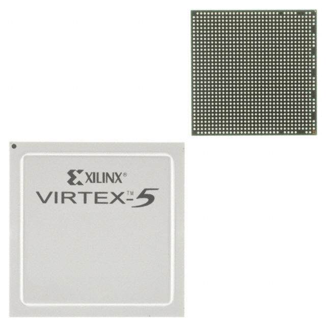
Xilinx Inc.(赛灵思)的XC6VLX75T-1FFG784C属于Virtex-6系列FPGA,是一款高性能、高密度的现场可编程门阵列。该型号的应用场景非常广泛,尤其适合对计算能力、信号处理和接口灵活性要求较高的领域。以下是其主要应用场景:

 1. 通信设备
   - 无线基站:支持复杂的信号处理任务,如调制解调、信道编码和解码等。
   - 网络交换机和路由器:实现数据包处理、流量管理以及高速网络接口功能。
   - 光纤通信:用于协议转换、数据同步和高速信号传输。

 2. 图像与视频处理
   - 视频编解码:支持实时高清或超高清视频的压缩与解压缩。
   - 图像增强:应用于工业视觉、医疗成像等领域,进行图像分析和处理。
   - 视频监控:实现多路视频流的采集、处理和传输。

 3. 军工与航空航天
   - 雷达系统:用于信号采集、处理和显示,支持复杂的波形生成和目标识别。
   - 卫星通信:提供高效的数据处理和抗辐射能力,适用于太空环境。
   - 导航系统:实现高精度的信号处理和数据融合。

 4. 工业自动化
   - 运动控制:支持复杂的算法运算,实现精确的电机控制。
   - 工业物联网(IIoT):作为边缘计算设备的核心,处理传感器数据并执行实时决策。
   - 机器人技术:用于路径规划、传感器融合和实时控制。

 5. 医疗设备
   - 医学影像:支持CT、MRI等设备中的图像重建和处理。
   - 实时监测:用于生命体征监测设备的数据采集与分析。

 6. 数据中心与云计算
   - 加速计算:作为协处理器,加速特定算法(如加密、数据分析)的运行。
   - 存储控制器:实现高效的存储管理和数据传输。

 7. 汽车电子
   - 高级驾驶辅助系统(ADAS):处理来自摄像头、雷达和激光雷达的大量数据。
   - 信息娱乐系统:支持多媒体处理和用户交互功能。

 8. 科学与研究
   - 高性能计算(HPC):用于模拟、建模和数据分析。
   - 基因测序:加速生物信息学中的数据处理任务。

XC6VLX75T-1FFG784C凭借其丰富的资源(逻辑单元、DSP Slice、RAM块等)、高速串行收发器(GTX)以及灵活的I/O配置,能够满足上述领域的多样化需求。同时,其低功耗特性和强大的性能使其成为许多嵌入式应用的理想选择。
| 参数 | 数值 |
| 产品目录 | 集成电路 (IC) |
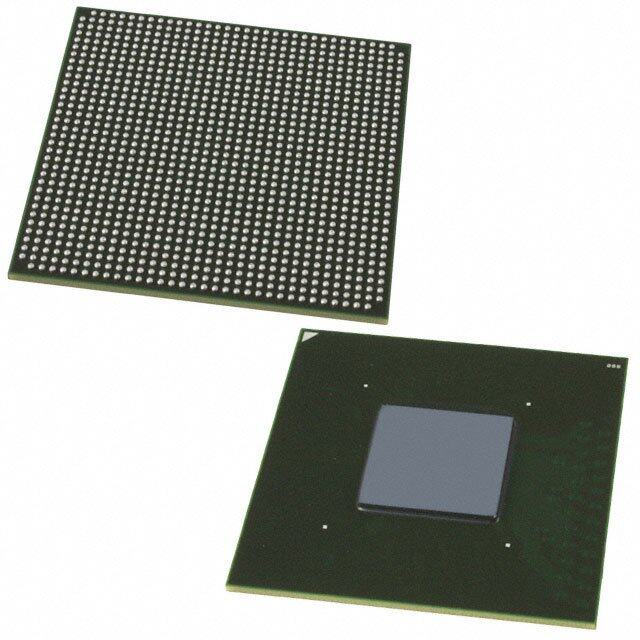
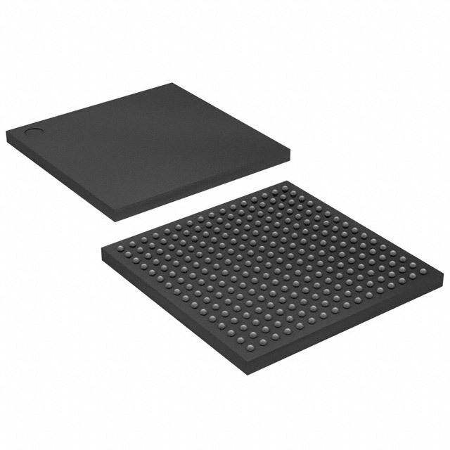
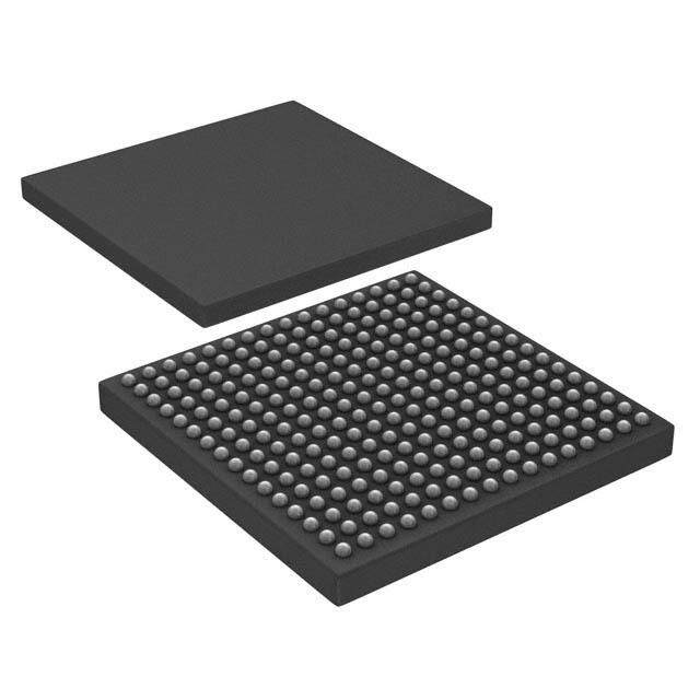
| 描述 | IC FPGA 360 I/O 784FCBGA |
| 产品分类 | |
| I/O数 | 360 |
| LAB/CLB数 | 5820 |
| 品牌 | Xilinx Inc |
| 数据手册 | |
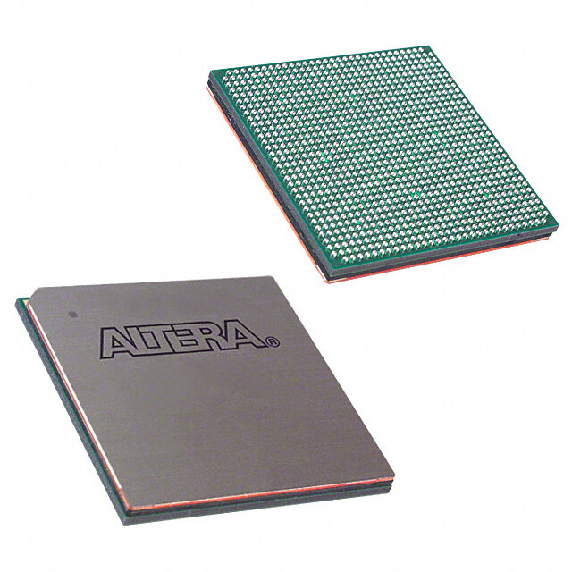
| 产品图片 |
|
| 产品型号 | XC6VLX75T-1FFG784C |
| PCN组件/产地 | |
| PCN设计/规格 | |
| rohs | 无铅 / 符合限制有害物质指令(RoHS)规范要求 |
| 产品系列 | Virtex® 6 LXT |
| 产品培训模块 | http://www.digikey.cn/PTM/IndividualPTM.page?site=cn&lang=zhs&ptm=25657 |
| 供应商器件封装 | 784-FCBGA |
| 其它名称 | 122-1787 |
| 安装类型 | 表面贴装 |
| 封装/外壳 | 784-BBGA,FCBGA |
| 工作温度 | 0°C ~ 85°C |
| 总RAM位数 | 5750784 |
| 栅极数 | - |
| 标准包装 | 36 |
| 电压-电源 | 0.95 V ~ 1.05 V |
| 逻辑元件/单元数 | 74496 |


- 商务部:美国ITC正式对集成电路等产品启动337调查
- 曝三星4nm工艺存在良率问题 高通将骁龙8 Gen1或转产台积电
- 太阳诱电将投资9.5亿元在常州建新厂生产MLCC 预计2023年完工
- 英特尔发布欧洲新工厂建设计划 深化IDM 2.0 战略
- 台积电先进制程称霸业界 有大客户加持明年业绩稳了
- 达到5530亿美元!SIA预计今年全球半导体销售额将创下新高
- 英特尔拟将自动驾驶子公司Mobileye上市 估值或超500亿美元
- 三星加码芯片和SET,合并消费电子和移动部门,撤换高东真等 CEO
- 三星电子宣布重大人事变动 还合并消费电子和移动部门
- 海关总署:前11个月进口集成电路产品价值2.52万亿元 增长14.8%

PDF Datasheet 数据手册内容提取
Virtex-6 FPGA Data Sheet: DC and Switching Characteristics DS152 (v3.6) March 18, 2014 Product Specification Virtex-6 FPGA Electrical Characteristics Virtex®-6 FPGAs are available in -3, -2, -1, and -1L speed grades, with -3 having the highest performance. Virtex-6 FPGA DC and AC characteristics are specified in commercial, extended, industrial, and military temperature ranges. Unless noted, the Virtex-6Q FPGA DC and AC characteristics are equivalent to the commercial specifications. Except for the operating temperature range or unless otherwise noted, all the DC and AC electrical parameters are the same for a particular speed grade (that is, the timing characteristics of a -1 speed grade industrial device are the same as for a -1 speed grade commercial device). However, only selected speed grades and/or devices are available in the extended, industrial, or military temperature ranges. All supply voltage and junction temperature specifications are representative of worst-case conditions. The parameters included are common to popular designs and typical applications. Available device and package combinations can be found at: (cid:129) DS150: Virtex-6 Family Overview (cid:129) DS155: Defense-Grade Virtex-6Q Family Overview This Virtex-6 FPGA data sheet, part of an overall set of documentation on the Virtex-6 FPGAs, is available on the Xilinx website at: www.xilinx.com/support/index.html/content/xilinx/en/supportNav/silicon_devices/fpga/virtex-6.html. Virtex-6 FPGA DC Characteristics Table 1: Absolute Maximum Ratings(1) Symbol Description Range Units Internal supply voltage relative to GND –0.5 to 1.1 V V CCINT For -1L devices: Internal supply voltage relative to GND –0.5 to 1.0 V V Auxiliary supply voltage relative to GND –0.5 to 3.0 V CCAUX V Output drivers supply voltage relative to GND –0.5 to 3.0 V CCO V Key memory battery backup supply –0.5 to 3.0 V BATT V External voltage supply for eFUSE programming(2) –0.5 to 3.0 V FS V Input reference voltage –0.5 to 3.0 V REF V (3) 2.5V or below I/O input voltage relative to GND(4) (user and dedicated I/Os) –0.5toV +0.5 V IN CCO V Voltage applied to 3-state 2.5V or below output(4) (user and dedicated I/Os) –0.5toV +0.5 V TS CCO T Storage temperature (ambient) –65to150 °C STG T Maximum soldering temperature(5) +220 °C SOL T Maximum junction temperature(5) +125 °C j Notes: 1. Stresses beyond those listed under Absolute Maximum Ratings might cause permanent damage to the device. These are stress ratings only, and functional operation of the device at these or any other conditions beyond those listed under Operating Conditions is not implied. Exposure to Absolute Maximum Ratings conditions for extended periods of time might affect device reliability. 2. When not programming eFUSE, connect V to GND. FS 3. 2.5V I/O absolute maximum limit applied to DC and AC signals. 4. For I/O operation, refer to UG361:Virtex-6 FPGA SelectIO Resources User Guide. 5. For soldering guidelines and thermal considerations, see UG365:Virtex-6 FPGA Packaging and Pinout Specification. © 2009–2014 Xilinx, Inc. XILINX, the Xilinx logo, Virtex, Zynq, Artix, Kintex, Spartan, ISE, Vivado and other designated brands included herein are trademarks of Xilinx in the United States and other countries. All other trademarks are the property of their respective owners. DS152 (v3.6) March 18, 2014 www.xilinx.com Product Specification 1
Virtex-6 FPGA Data Sheet: DC and Switching Characteristics Table 2: Recommended Operating Conditions Symbol Description Min Max Units Internal supply voltage relative to GND for all devices except -1L devices. 0.95 1.05 V For -1L commercial temperature range devices: internal supply voltage relative 0.87 0.93 V V to GND, T =0°C to +85°C CCINT j For -1L industrial temperature range devices: internal supply voltage relative to GND, 0.91 0.97 V T =–40°C to +100°C j V Auxiliary supply voltage relative to GND 2.375 2.625 V CCAUX V (1)(2)(3) Supply voltage relative to GND 1.14 2.625 V CCO 2.5V supply voltage relative to GND GND–0.20 2.625 V V IN 2.5V and below supply voltage relative to GND GND–0.20 V +0.2 V CCO Maximum current through any pin in a powered or unpowered bank when forward – 10 mA I (5) IN biasing the clamp diode. V (6) Battery voltage relative to GND 1.0 2.5 V BATT V (7) External voltage supply for eFUSE programming 2.375 2.625 V FS Junction temperature operating range for commercial (C) temperature devices 0 85 °C Junction temperature operating range for extended (E) temperature devices 0 100 °C T j Junction temperature operating range for industrial (I) temperature devices –40 100 °C Junction temperature operating range for military (M) temperature devices –55 125 °C Notes: 1. Configuration data is retained even if V drops to 0V. CCO 2. Includes V of 1.2V, 1.5V, 1.8V, and 2.5V. CCO 3. The configuration supply voltage V is also known as V . CC_CONFIG CCO_0 4. All voltages are relative to ground. 5. A total of 100mA per bank should not be exceeded. 6. V is required only when using bitstream encryption. If battery is not used, connect V to either ground or V . BATT BATT CCAUX 7. During eFUSE programming, V must be within the recommended operating range and T =+15°C to +85°C. Otherwise, V can be FS j FS connected to GND. DS152 (v3.6) March 18, 2014 www.xilinx.com Product Specification 2
Virtex-6 FPGA Data Sheet: DC and Switching Characteristics Table 3: DC Characteristics Over Recommended Operating Conditions(1)(2) Symbol Description Min Typ Max Units V Data retention V voltage (below which configuration data might be lost) 0.75 – – V DRINT CCINT V Data retention V voltage (below which configuration data might be lost) 2.0 – – V DRI CCAUX I V leakage current per pin – – 10 µA REF REF I Input or output leakage current per pin (sample-tested) – – 10 µA L C (3) Die input capacitance at the pad – – 8 pF IN Pad pull-up (when selected) @ V =0V, V =2.5V 20 – 80 µA IN CCO Pad pull-up (when selected) @ V =0V, V =1.8V 8 – 40 µA IN CCO I RPU Pad pull-up (when selected) @ V =0V, V =1.5V 5 – 30 µA IN CCO Pad pull-up (when selected) @ V =0V, V =1.2V 1 – 20 µA IN CCO I Pad pull-down (when selected) @ V =2.5V 3 – 80 µA RPD IN I Battery supply current – – 150 nA BATT n Temperature diode ideality factor – 1.0002 – n r Series resistance – 5 – Ω Notes: 1. Typical values are specified at nominal voltage, 25°C. 2. Maximum value specified for worst case process at 25°C. 3. This measurement represents the die capacitance at the pad, not including the package. DS152 (v3.6) March 18, 2014 www.xilinx.com Product Specification 3
Virtex-6 FPGA Data Sheet: DC and Switching Characteristics Important Note Typical values for quiescent supply current are specified at nominal voltage, 85°C junction temperatures (T). Xilinx j recommends analyzing static power consumption at T =85°C because the majority of designs operate near the high end of j the commercial temperature range. Quiescent supply current is specified by speed grade for Virtex-6 devices. Use the Xilinx Power Estimator (XPE) spreadsheet tool (download at http://www.xilinx.com/power) to calculate static power consumption for conditions other than those specified in Table4. Table 4: Typical Quiescent Supply Current Speed and Temperature Grade Symbol Description Device Units -3 (C) -2 (C, E, & I) -1 (C & I) -1 (I & M)(2) -1L (C) -1L (I)(1) I Quiescent V XC6VLX75T 927 927 927 N/A 656 741 mA CCINTQ CCINT supply current XC6VLX130T 1563 1563 1563 N/A 1102 1245 mA XC6VLX195T 2059 2059 2059 N/A 1441 1628 mA XC6VLX240T 2478 2478 2478 N/A 1733 1957 mA XC6VLX365T 3001 3001 3001 N/A 2092 2363 mA XC6VLX550T(3) N/A 4515 4515 N/A 3147 3555 mA XC6VLX760(3) N/A 5094 5094 N/A 3471 3921 mA XC6VSX315T 3476 3476 3476 N/A 2409 2721 mA XC6VSX475T(3) N/A 5227 5227 N/A 3622 4091 mA XC6VHX250T 2906 2906 2906 N/A N/A N/A mA XC6VHX255T 2746 2746 2746 N/A N/A N/A mA XC6VHX380T(4) 4160 4160 4160 N/A N/A N/A mA XC6VHX565T(5) N/A 5207 5207 N/A N/A N/A mA XQ6VLX130T N/A 1563 N/A 1563 N/A 1245 mA XQ6VLX240T N/A 2478 N/A 2478 N/A 1957 mA XQ6VLX550T(7) N/A N/A N/A 4515 N/A 3555 mA XQ6VSX315T N/A 3476 N/A 3476 N/A 2721 mA XQ6VSX475T(7) N/A N/A N/A 5227 N/A 4091 mA DS152 (v3.6) March 18, 2014 www.xilinx.com Product Specification 4
Virtex-6 FPGA Data Sheet: DC and Switching Characteristics Table 4: Typical Quiescent Supply Current (Cont’d) Speed and Temperature Grade Symbol Description Device Units -3 (C) -2 (C, E, & I) -1 (C & I) -1 (I & M)(2) -1L (C) -1L (I)(1) I Quiescent V XC6VLX75T 1 1 1 N/A 1 1 mA CCOQ CCO supply current XC6VLX130T 1 1 1 N/A 1 1 mA XC6VLX195T 1 1 1 N/A 1 1 mA XC6VLX240T 2 2 2 N/A 2 2 mA XC6VLX365T 2 2 2 N/A 2 2 mA XC6VLX550T(3) N/A 3 3 N/A 3 3 mA XC6VLX760(3) N/A 3 3 N/A 3 3 mA XC6VSX315T 2 2 2 N/A 2 2 mA XC6VSX475T(3) N/A 2 2 N/A 2 2 mA XC6VHX250T 1 1 1 N/A N/A N/A mA XC6VHX255T 1 1 1 N/A N/A N/A mA XC6VHX380T(4) 2 2 2 N/A N/A N/A mA XC6VHX565T(5) N/A 2 2 N/A N/A N/A mA XQ6VLX130T N/A 1 N/A 1 N/A 1 mA XQ6VLX240T N/A 2 N/A 2 N/A 2 mA XQ6VLX550T(7) N/A N/A N/A 3 N/A 3 mA XQ6VSX315T N/A 2 N/A 2 N/A 2 mA XQ6VSX475T(7) N/A N/A N/A 2 N/A 2 mA DS152 (v3.6) March 18, 2014 www.xilinx.com Product Specification 5
Virtex-6 FPGA Data Sheet: DC and Switching Characteristics Table 4: Typical Quiescent Supply Current (Cont’d) Speed and Temperature Grade Symbol Description Device Units -3 (C) -2 (C, E, & I) -1 (C & I) -1 (I & M)(2) -1L (C) -1L (I)(1) I Quiescent V XC6VLX75T 45 45 45 N/A 45 45 mA CCAUXQ CCAUX supply current XC6VLX130T 75 75 75 N/A 75 75 mA XC6VLX195T 113 113 113 N/A 113 113 mA XC6VLX240T 135 135 135 N/A 135 135 mA XC6VLX365T 191 191 191 N/A 191 191 mA XC6VLX550T(3) N/A 286 286 N/A 286 286 mA XC6VLX760(3) N/A 387 387 N/A 387 387 mA XC6VSX315T 186 186 186 N/A 186 186 mA XC6VSX475T(3) N/A 279 279 N/A 279 279 mA XC6VHX250T 152 152 152 N/A N/A N/A mA XC6VHX255T 152 152 152 N/A N/A N/A mA XC6VHX380T(4) 227 227 227 N/A N/A N/A mA XC6VHX565T(5) N/A 315 315 N/A N/A N/A mA XQ6VLX130T(6) N/A 75 N/A 75 N/A 75 mA XQ6VLX240T(6) N/A 135 N/A 135 N/A 135 mA XQ6VLX550T(7) N/A N/A N/A 286 N/A 286 mA XQ6VSX315T(6) N/A 186 N/A 186 N/A 186 mA XQ6VSX475T(7) N/A N/A N/A 279 N/A 279 mA Notes: 1. Typical values are specified at nominal voltage, 85°C junction temperatures (T). -1 and -2 industrial (I) grade devices have the same typical j values as commercial (C) grade devices at 85°C, but higher values at 100°C. Use the XPE tool to calculate 100°C values. -1L industrial temperature range devices have the values specified in this column. 2. Use the XPE tool to calculate 125°C values for -1M temperature range devices. 3. The -2E extended temperature range (T =0°C to +100°C) is only available in these devices. The -2I temperature range (T =–40°C to j j +100°C) is available for all other devices except the XC6VHX565T. 4. The XC6VHX380T is available with both -2E and -2I temperature ranges. 5. The XC6VHX565T is only available in the following temperature ranges: -1C, -1I, -2C, and -2E. 6. The XQ6VLX130T, XQ6VLX240T, and XQ6VSX315T are available in -2I, -1I, -1M, and -1LI temperature ranges. 7. The XQ6VLX550T and the XQ6VSX475T are only available in -1I and -1LI temperature ranges. 8. Typical values are for blank configured devices with no output current loads, no active input pull-up resistors, all I/O pins are 3-state and floating. 9. If DCI or differential signaling is used, more accurate quiescent current estimates can be obtained by using the XPE or XPower Analyzer (XPA) tools. Power-On Power Supply Requirements Xilinx FPGAs require a certain amount of supply current during power-on to insure proper device initialization. The actual current consumed depends on the power-on sequence and ramp rate of the power supply. The recommended power-on sequence for Virtex-6 devices is V , V , and V to meet the power-up current CCINT CCAUX CCO requirements listed in Table5. V can be powered up or down at any time, but power up current specifications can vary CCINT from Table5. The device will have no physical damage or reliability concerns if V , V , and V sequence cannot CCINT CCAUX CCO be followed. If the recommended power-up sequence cannot be followed and the I/Os must remain 3-stated throughout configuration, then V must be powered prior to V or V and V must be powered by the same supply. Similarly, for power- CCAUX CCO CCAUX CCO down, the reverse V and V sequence is recommended if the I/Os are to remain 3-stated. CCAUX CCO DS152 (v3.6) March 18, 2014 www.xilinx.com Product Specification 6
Virtex-6 FPGA Data Sheet: DC and Switching Characteristics The GTH transceiver supplies must be powered using a MGTHAVCC, MGTHAVCCRX, MGTHAVCCPLL, and MGTHAVTT sequence. There are no sequencing requirement for these supplies with respect to the other FPGA supply voltages. For more detail see Table27: GTH Transceiver Power Supply Sequencing. There are no sequencing requirements for the GTX transceivers power supplies. Table5 shows the minimum current, in addition to I , that are required by Virtex-6 devices for proper power-on and CCQ configuration. If the current minimums shown in Table4 and Table5 are met, the device powers on after all three supplies have passed through their power-on reset threshold voltages. The FPGA must be configured after applying V , V , CCINT CCAUX and V for the appropriate configuration banks. Once initialized and configured, use the XPE tools to estimate current CCO drain on these supplies. Table 5: Power-On Current for Virtex-6 Devices I I I CCINTMIN CCAUXMIN CCOMIN Device Units Typ(1) Typ(1) Typ(1) XC6VLX75T See I in Table4 I +10 I +30mA per bank mA CCINTQ CCAUXQ CCOQ XC6VLX130T See I in Table4 I +10 I +30mA per bank mA CCINTQ CCAUXQ CCOQ XC6VLX195T See I in Table4 I +40 I +30mA per bank mA CCINTQ CCAUXQ CCOQ XC6VLX240T See I in Table4 I +40 I +30mA per bank mA CCINTQ CCAUXQ CCOQ XC6VLX365T See I in Table4 I +40 I +30mA per bank mA CCINTQ CCAUXQ CCOQ XC6VLX550T See I in Table4 I +40 I +30mA per bank mA CCINTQ CCAUXQ CCOQ XC6VLX760 See I in Table4 I +40 I +30mA per bank mA CCINTQ CCAUXQ CCOQ XC6VSX315T See I in Table4 I +40 I +30mA per bank mA CCINTQ CCAUXQ CCOQ XC6VSX475T See I in Table4 I +50 I +30mA per bank mA CCINTQ CCAUXQ CCOQ XC6VHX250T See I in Table4 I +40 I +30mA per bank mA CCINTQ CCAUXQ CCOQ XC6VHX255T See I in Table4 I +40 I +30mA per bank mA CCINTQ CCAUXQ CCOQ XC6VHX380T See I in Table4 I +40 I +30mA per bank mA CCINTQ CCAUXQ CCOQ XC6VHX565T See I in Table4 I +40 I +30mA per bank mA CCINTQ CCAUXQ CCOQ XQ6VLX130T See I in Table4 I +100 I +30mA per bank mA CCINTQ CCAUXQ CCOQ XQ6VLX240T See I in Table4 I +100 I +30mA per bank mA CCINTQ CCAUXQ CCOQ XQ6VLX550T See I in Table4 I +100 I +30mA per bank mA CCINTQ CCAUXQ CCOQ XQ6VSX315T See I in Table4 I +100 I +40mA per bank mA CCINTQ CCAUXQ CCOQ XQ6VSX475T See I in Table4 I +100 I +40mA per bank mA CCINTQ CCAUXQ CCOQ Notes: 1. Typical values are specified at nominal voltage, 25°C. 2. Use the Xilinx Power Estimator (XPE) spreadsheet tool (download at http://www.xilinx.com/power) to calculate maximum power-on currents. Table 6: Power Supply Ramp Time Symbol Description Ramp Time Units V Internal supply voltage relative to GND 0.20 to 50.0 ms CCINT V Output drivers supply voltage relative to GND 0.20 to 50.0 ms CCO V Auxiliary supply voltage relative to GND 0.20 to 50.0 ms CCAUX DS152 (v3.6) March 18, 2014 www.xilinx.com Product Specification 7
Virtex-6 FPGA Data Sheet: DC and Switching Characteristics SelectIO™ DC Input and Output Levels Values for V and V are recommended input voltages. Values for I and I are guaranteed over the recommended IL IH OL OH operating conditions at the V and V test points. Only selected standards are tested. These are chosen to ensure that OL OH all standards meet their specifications. The selected standards are tested at a minimum V with the respective V and CCO OL V voltage levels shown. Other standards are sample tested. OH Table 7: SelectIO DC Input and Output Levels V V V V I I IL IH OL OH OL OH I/O Standard V, Min V, Max V, Min V, Max V, Max V, Min mA mA LVCMOS25, –0.3 0.7 1.7 V +0.3 0.4 V –0.4 Note(3) Note(3) CCO CCO LVDCI25 LVCMOS18, –0.3 35% V 65% V V +0.3 0.45 V –0.45 Note(4) Note(4) CCO CCO CCO CCO LVDCI18 LVCMOS15, –0.3 35% V 65% V V +0.3 25%V 75%V Note(4) Note(4) CCO CCO CCO CCO CCO LVDCI15 LVCMOS12 –0.3 35% V 65% V V +0.3 25%V 75%V Note(5) Note(5) CCO CCO CCO CCO CCO HSTLI_12 –0.3 V –0.1 V +0.1 V +0.3 25%V 75%V 6.3 –6.3 REF REF CCO CCO CCO HSTLI(2) –0.3 V –0.1 V +0.1 V +0.3 0.4 V –0.4 8 –8 REF REF CCO CCO HSTLII(2) –0.3 V –0.1 V +0.1 V +0.3 0.4 V –0.4 16 –16 REF REF CCO CCO HSTLIII(2) –0.3 V –0.1 V +0.1 V +0.3 0.4 V –0.4 24 –8 REF REF CCO CCO DIFFHSTLI(2) –0.3 50% V –0.1 50% V +0.1 V +0.3 – – – – CCO CCO CCO DIFFHSTLII(2) –0.3 50% V –0.1 50% V +0.1 V +0.3 – – – – CCO CCO CCO SSTL2I –0.3 V –0.15 V +0.15 V +0.3 V –0.61 V +0.61 8.1 –8.1 REF REF CCO TT TT SSTL2II –0.3 V –0.15 V +0.15 V +0.3 V –0.81 V +0.81 16.2 –16.2 REF REF CCO TT TT DIFFSSTL2I –0.3 50% 50% V +0.3 – – – – CCO V –0.15 V +0.15 CCO CCO DIFFSSTL2II –0.3 50% 50% V +0.3 – – – – CCO V –0.15 V +0.15 CCO CCO SSTL18I –0.3 V –0.125 V +0.125 V +0.3 V –0.47 V +0.47 6.7 –6.7 REF REF CCO TT TT SSTL18II –0.3 V –0.125 V +0.125 V +0.3 V –0.60 V +0.60 13.4 –13.4 REF REF CCO TT TT DIFFSSTL18I –0.3 50% 50% V +0.3 – – – – CCO V –0.125 V +0.125 CCO CCO DIFFSSTL18II –0.3 50% 50% V +0.3 – – – – CCO V –0.125 V +0.125 CCO CCO SSTL15 –0.3 V –0.1 V +0.1 V +0.3 V –0.175 V +0.175 14.3 –14.3 REF REF CCO TT TT DIFFSSTL15 –0.3 50% V –0.1 50% V +0.1 V +0.3 – – – – CCO CCO CCO Notes: 1. Tested according to relevant specifications. 2. Applies to both 1.5V and 1.8V HSTL. 3. Using drive strengths of 2, 4, 6, 8, 12, 16, or 24mA. 4. Using drive strengths of 2, 4, 6, 8, 12, or 16mA. 5. Supported drive strengths of 2, 4, 6, or 8mA. 6. For detailed interface specific DC voltage levels, see UG361:Virtex-6 FPGA SelectIO Resources User Guide. DS152 (v3.6) March 18, 2014 www.xilinx.com Product Specification 8
Virtex-6 FPGA Data Sheet: DC and Switching Characteristics HT DC Specifications (HT_25) Table 8: HT DC Specifications Symbol DC Parameter Conditions Min Typ Max Units V Supply Voltage 2.38 2.5 2.63 V CCO V Differential Output Voltage for XC devices R = 100Ω across Q and Q signals 480 600 885 mV OD T Differential Output Voltage for XQ devices 480 600 930 mV Δ V Change in V Magnitude –15 – 15 mV OD OD V Output Common Mode Voltage R = 100Ω across Q and Q signals 440 600 760 mV OCM T Δ V Change in V Magnitude –15 – 15 mV OCM OCM V Input Differential Voltage 200 600 1000 mV ID Δ V Change in V Magnitude –15 – 15 mV ID ID V Input Common Mode Voltage 440 600 780 mV ICM Δ V Change in V Magnitude –15 – 15 mV ICM ICM LVDS DC Specifications (LVDS_25) Table 9: LVDS DC Specifications Symbol DC Parameter Conditions Min Typ Max Units V Supply Voltage 2.38 2.5 2.63 V CCO V Output High Voltage for Q and Q R = 100Ω across Q and Q signals – – 1.675 V OH T V Output Low Voltage for Q and Q R = 100Ω across Q and Q signals 0.825 – – V OL T V Differential Output Voltage (Q–Q), R = 100Ω across Q and Q signals 247 350 600 mV ODIFF T Q = High (Q–Q), Q=High V Output Common-Mode Voltage for XC devices R = 100Ω across Q and Q signals 1.075 1.250 1.425 V OCM T Output Common-Mode Voltage for XQ devices 1.000 1.250 1.425 V V Differential Input Voltage (Q–Q), 100 350 600 mV IDIFF Q = High (Q–Q), Q=High V Input Common-Mode Voltage 0.3 1.2 2.2 V ICM Extended LVDS DC Specifications (LVDSEXT_25) Table 10: Extended LVDS DC Specifications Symbol DC Parameter Conditions Min Typ Max Units V Supply Voltage 2.38 2.5 2.63 V CCO V Output High Voltage for Q and Q R = 100Ω across Q and Q signals – – 1.785 V OH T V Output Low Voltage for Q and Q R = 100Ω across Q and Q signals 0.715 – – V OL T V Differential Output Voltage (Q–Q), R = 100Ω across Q and Q signals 350 – 840 mV ODIFF T Q = High (Q–Q), Q=High for XC devices Differential Output Voltage (Q–Q), 350 – 850 mV Q = High (Q–Q), Q=High for XQ devices V Output Common-Mode Voltage for XC devices R = 100Ω across Q and Q signals 1.075 1.250 1.425 V OCM T Output Common-Mode Voltage for XQ devices 1.000 1.250 1.425 V V Differential Input Voltage (Q–Q), Common-mode input 100 – 1000 mV IDIFF Q = High (Q–Q), Q=High voltage=1.25V V Input Common-Mode Voltage Differential input voltage=±350mV 0.3 1.2 2.2 V ICM DS152 (v3.6) March 18, 2014 www.xilinx.com Product Specification 9
Virtex-6 FPGA Data Sheet: DC and Switching Characteristics LVPECL DC Specifications (LVPECL_25) These values are valid when driving a 100Ω differential load only, i.e., a 100Ω resistor between the two receiver pins. The V levels are 200mV below standard LVPECL levels and are compatible with devices tolerant of lower common-mode OH ranges. Table11 summarizes the DC output specifications of LVPECL. For more information on using LVPECL, see UG361: Virtex-6 FPGA SelectIO Resources User Guide. Table 11: LVPECL DC Specifications Symbol DC Parameter Min Typ Max Units V Output High Voltage V –1.025 1.545 V –0.88 V OH CC CC V Output Low Voltage V –1.81 0.795 V –1.62 V OL CC CC V Input Common-Mode Voltage 0.6 – 2.2 V ICM V Differential Input Voltage(1)(2) 0.100 – 1.5 V IDIFF Notes: 1. Recommended input maximum voltage not to exceed V +0.2V. CCAUX 2. Recommended input minimum voltage not to go below –0.5V. eFUSE Read Endurance Table12 lists the maximum number of read cycle operations expected. For more information, see UG360:Virtex-6 FPGA Configuration User Guide. Table 12: eFUSE Read Endurance Speed Grade Symbol Description Units -3 -2 -1 -1L DNA_CYCLES Number of DNA_PORT READ operations or JTAG ISC_DNA read Read 30,000,000 command operations. Unaffected by SHIFT operations. Cycles AES_CYCLES Number of JTAG FUSE_KEY or FUSE_CNTL read command 30,000,000 Read operations. Unaffected by SHIFT operations. Cycles DS152 (v3.6) March 18, 2014 www.xilinx.com Product Specification 10
Virtex-6 FPGA Data Sheet: DC and Switching Characteristics GTX Transceiver Specifications GTX Transceiver DC Characteristics Table 13: Absolute Maximum Ratings for GTX Transceivers(1) Symbol Description Min Max Units Analog supply voltage for the GTX transmitter and receiver circuits relative to –0.5 1.1 V MGTAVCC GND Analog supply voltage for the GTX transmitter and receiver termination circuits –0.5 1.32 V MGTAVTT relative to GND Analog supply voltage for the resistor calibration circuit of the GTX transceiver –0.5 1.32 V MGTAVTTRCAL column V Receiver (RXP/RXN) and Transmitter (TXP/TXN) absolute input voltage –0.5 1.32 V IN V Reference clock absolute input voltage –0.5 1.32 V MGTREFCLK Notes: 1. Stresses beyond those listed under Absolute Maximum Ratings might cause permanent damage to the device. These are stress ratings only, and functional operation of the device at these or any other conditions beyond those listed under Operating Conditions is not implied. Exposure to Absolute Maximum Ratings conditions for extended periods of time might affect device reliability. Table 14: Recommended Operating Conditions for GTX Transceivers(1)(2) Speed PLL Symbol Description Min Typ Max Units Grade Frequency -3, -2(3) >2.7 GHz 1.0 1.03 1.06 V Analog supply voltage for the GTX transmitter -3, -2(3) ≤2.7 GHz 0.95 1.0 1.06 V MGTAVCC and receiver circuits relative to GND -1 ≤2.7 GHz 0.95 1.0 1.06 V -1L ≤2.7 GHz 0.95 1.0 1.05 V Analog supply voltage for the GTX transmitter MGTAVTT All – 1.14 1.2 1.26 V and receiver termination circuits relative to GND Analog supply voltage for the resistor calibration MGTAVTTRCAL All – 1.14 1.2 1.26 V circuit of the GTX transceiver column Notes: 1. Each voltage listed requires the filter circuit described in UG366:Virtex-6 FPGA GTX Transceivers User Guide. 2. Voltages are specified for the temperature range of T = –40°C to +100°C for all XC devices and T = –55°C to +125°C for the XQ devices j j 3. If a GTX Quad contains transceivers operating with a mixture of PLL frequencies above and below 2.7GHz, the MGTAVCC voltage supply must be in the range of 1.0V to 1.06V. Table 15: GTX Transceiver Supply Current (per Lane)(1)(2) Symbol Description Typ Max Units I MGTAVTT supply current for one GTX transceiver 55.9 mA MGTAVTT Note 2 I MGTAVCC supply current for one GTX transceiver 56.1 mA MGTAVCC MGTR Precision reference resistor for internal calibration termination 100.0 ±1% tolerance Ω REF Notes: 1. Typical values are specified at nominal voltage, 25°C, with a 3.125Gb/s line rate. 2. Values for currents of other transceiver configurations and conditions can be obtained by using the Xilinx Power Estimator (XPE) or XPower Analyzer (XPA) tools. DS152 (v3.6) March 18, 2014 www.xilinx.com Product Specification 11
Virtex-6 FPGA Data Sheet: DC and Switching Characteristics Table 16: GTX Transceiver Quiescent Supply Current (per Lane)(1)(2)(3) Symbol Description Typ(4) Max Units I Quiescent MGTAVTT supply current for one GTX transceiver 0.9 mA MGTAVTTQ Note 2 I Quiescent MGTAVCC supply current for one GTX transceiver 3.5 mA MGTAVCCQ Notes: 1. Device powered and unconfigured. 2. Currents for conditions other than values specified in this table can be obtained by using the XPE or XPA tools. 3. GTX transceiver quiescent supply current for an entire device can be calculated by multiplying the values in this table by the number of available GTX transceivers. 4. Typical values are specified at nominal voltage, 25°C. GTX Transceiver DC Input and Output Levels Table17 summarizes the DC output specifications of the GTX transceivers in Virtex-6 FPGAs. Consult UG366:Virtex-6 FPGA GTX Transceivers User Guide for further details. Table 17: GTX Transceiver DC Specifications Symbol DC Parameter Conditions Min Typ Max Units Differential peak-to-peak input External AC coupled ≤4.25Gb/s 125 – 2000 mV DVPPIN voltage External AC coupled >4.25Gb/s 175 – 2000 mV Absolute input voltage DC coupled –400 – MGTAVTT mV V IN MGTAVTT=1.2V Common mode input voltage DC coupled – 2/3 MGTAVTT – mV V CMIN MGTAVTT=1.2V Differential peak-to-peak output Transmitter output swing is set to – – 1000 mV DV PPOUT voltage(1) maximum setting DC common mode output Equation based MGTAVTT–DV /4 mV V PPOUT CMOUTDC voltage. R Differential input resistance 80 100 130 Ω IN R Differential output resistance 80 100 120 Ω OUT T Transmitter output pair (TXP and TXN) intra-pair skew – 2 8 ps OSKEW C Recommended external AC coupling capacitor(2) – 100 – nF EXT Notes: 1. The output swing and preemphasis levels are programmable using the attributes discussed in UG366:Virtex-6 FPGA GTX Transceivers User Guide and can result in values lower than reported in this table. 2. Other values can be used as appropriate to conform to specific protocols and standards. X-Ref Target - Figure 1 +V P Single-Ended N Voltage 0 ds152_01_121509 Figure 1: Single-Ended Peak-to-Peak Voltage DS152 (v3.6) March 18, 2014 www.xilinx.com Product Specification 12
Virtex-6 FPGA Data Sheet: DC and Switching Characteristics X-Ref Target - Figure 2 +V Differential 0 Voltage –V P–N ds152_02_121509 Figure 2: Differential Peak-to-Peak Voltage Table18 summarizes the DC specifications of the clock input of the GTX transceiver. Consult UG366:Virtex-6 FPGA GTX Transceivers User Guide for further details. Table 18: GTX Transceiver Clock DC Input Level Specification Symbol DC Parameter Min Typ Max Units V Differential peak-to-peak input voltage 210 800 2000 mV IDIFF R Differential input resistance 90 100 130 Ω IN C Required external AC coupling capacitor(1) – 100 – nF EXT Notes: 1. Other values can be used as appropriate to conform to specific protocols and standards. GTX Transceiver Switching Characteristics Consult UG366:Virtex-6 FPGA GTX Transceivers User Guide for further information. Table 19: GTX Transceiver Performance Speed Grade Symbol Description Units -3 -2 -1 -1L F Maximum GTX transceiver data rate 6.6 6.6 5.0 5.0 Gb/s GTXMAX F Maximum PLL frequency 3.3(1) 3.3(1) 2.7 2.7 GHz GPLLMAX F Minimum PLL frequency 1.2 1.2 1.2 1.2 GHz GPLLMIN Notes: 1. See Table14 for MGTAVCC requirements when PLL frequency is greater than 2.7GHz. Table 20: GTX Transceiver Dynamic Reconfiguration Port (DRP) Switching Characteristics Speed Grade Symbol Description Units -3 -2 -1 -1L F GTXDRPCLK maximum frequency 150 150 125 100 MHz GTXDRPCLK DS152 (v3.6) March 18, 2014 www.xilinx.com Product Specification 13
Virtex-6 FPGA Data Sheet: DC and Switching Characteristics Table 21: GTX Transceiver Reference Clock Switching Characteristics All Speed Grades Symbol Description Conditions Units Min Typ Max F Reference clock frequency range 62.5 – 650 MHz GCLK T Reference clock rise time 20%–80% – 200 – ps RCLK T Reference clock fall time 80%–20% – 200 – ps FCLK T Reference clock duty cycle Transceiver PLL only 45 50 55 % DCREF Clock recovery frequency acquisition – – 1 ms T Initial PLL lock LOCK time Lock to data after PLL has locked – – 200 µs T Clock recovery phase acquisition time PHASE to the reference clock X-Ref Target - Figure 3 T RCLK 80% 20% T FCLK ds152_05_042109 Figure 3: Reference Clock Timing Parameters Table 22: GTX Transceiver User Clock Switching Characteristics(1) Speed Grade Symbol Description Conditions Units -3 -2 -1 -1L Internal 20-bit data path 330 330 250 250 MHz F TXOUTCLK maximum frequency TXOUT Internal 16-bit data path 412.5 412.5 312.5 250 MHz Internal 20-bit data path 330 330 250 250 MHz F RXRECCLK maximum frequency RXREC Internal 16-bit data path 412.5 412.5 312.5 250 MHz T RXUSRCLK maximum frequency 412.5(2) 412.5(2) 312.5 250 MHz RX 1 byte interface 376 376 312.5 250 MHz T RXUSRCLK2 maximum frequency 2 byte interface 406.25 406.25 312.5 250 MHz RX2 4 byte interface 206.25 206.25 156.25 125 MHz T TXUSRCLK maximum frequency 412.5(3) 412.5(3) 312.5 250 MHz TX 1 byte interface 376 376 312.5 250 MHz T TXUSRCLK2 maximum frequency 2 byte interface 406.25 406.25 312.5 250 MHz TX2 4 byte interface 206.25 206.25 156.25 125 MHz Notes: 1. Clocking must be implemented as described in UG366:Virtex-6 FPGA GTX Transceivers User Guide. 2. 406.25MHz when the RX elastic buffer is bypassed. 3. 406.25MHz when the TX buffer is bypassed. DS152 (v3.6) March 18, 2014 www.xilinx.com Product Specification 14
Virtex-6 FPGA Data Sheet: DC and Switching Characteristics Table 23: GTX Transceiver Transmitter Switching Characteristics Symbol Description Condition Min Typ Max Units F Serial data rate range 0.480 – F Gb/s GTXTX GTXMAX T TX Rise time 20%–80% – 120 – ps RTX T TX Fall time 80%–20% – 120 – ps FTX T TX lane-to-lane skew(1) – – 350 ps LLSKEW V Electrical idle amplitude – – 15 mV TXOOBVDPP T Electrical idle transition time – – 75 ns TXOOBTRANSITION TJ Total Jitter(2)(3) – – 0.33 UI 6.5 6.5Gb/s DJ Deterministic Jitter(2)(3) – – 0.17 UI 6.5 TJ Total Jitter(2)(3) – – 0.33 UI 5.0 5.0Gb/s DJ Deterministic Jitter(2)(3) – – 0.15 UI 5.0 TJ Total Jitter(2)(3) – – 0.33 UI 4.25 4.25Gb/s DJ Deterministic Jitter(2)(3) – – 0.14 UI 4.25 TJ Total Jitter(2)(3) – – 0.34 UI 3.75 3.75Gb/s DJ Deterministic Jitter(2)(3) – – 0.16 UI 3.75 TJ Total Jitter(2)(3) – – 0.2 UI 3.125 3.125Gb/s DJ Deterministic Jitter(2)(3) – – 0.1 UI 3.125 TJ Total Jitter(2)(3) – – 0.35 UI 3.125L 3.125Gb/s(4) DJ Deterministic Jitter(2)(3) – – 0.16 UI 3.125L TJ Total Jitter(2)(3) – – 0.20 UI 2.5 2.5Gb/s(5) DJ Deterministic Jitter(2)(3) – – 0.08 UI 2.5 TJ Total Jitter(2)(3) – – 0.15 UI 1.25 1.25Gb/s(6) DJ Deterministic Jitter(2)(3) – – 0.06 UI 1.25 TJ Total Jitter(2)(3) – – 0.1 UI 600 600Mb/s DJ Deterministic Jitter(2)(3) – – 0.03 UI 600 TJ Total Jitter(2)(3) – – 0.1 UI 480 480Mb/s DJ Deterministic Jitter(2)(3) – – 0.03 UI 480 Notes: 1. Using same REFCLK input with TXENPMAPHASEALIGN enabled for up to 12 consecutive transmitters (three fully populated GTX Quads). 2. Using PLL_DIVSEL_FB=2, 20-bit internal data width. These values are NOT intended for protocol specific compliance determinations. 3. All jitter values are based on a bit-error ratio of 1e-12. 4. PLL frequency at 1.5625GHz and OUTDIV=1. 5. PLL frequency at 2.5GHz and OUTDIV=2. 6. PLL frequency at 2.5GHz and OUTDIV=4. DS152 (v3.6) March 18, 2014 www.xilinx.com Product Specification 15
Virtex-6 FPGA Data Sheet: DC and Switching Characteristics Table 24: GTX Transceiver Receiver Switching Characteristics Symbol Description Min Typ Max Units RX oversampler not enabled 0.600 – F Gb/s GTXMAX F Serial data rate GTXRX RX oversampler enabled 0.480 – 0.600 Gb/s T Time for RXELECIDLE to respond to loss or restoration of data – 75 – ns RXELECIDLE RX OOB detect threshold peak-to-peak 60 – 150 mV OOBVDPP Receiver spread-spectrum –5000 – 0 ppm RX Modulated @ 33KHz SST tracking(1) RX Run length (CID) Internal AC capacitor bypassed – – 512 UI RL Data/REFCLK PPM offset CDR 2nd-order loop disabled –200 – 200 ppm RX PPMTOL tolerance CDR 2nd-order loop enabled –2000 – 2000 ppm SJ Jitter Tolerance(2) JT_SJ Sinusoidal Jitter(3) 6.5Gb/s 0.44 – – UI 6.5 JT_SJ Sinusoidal Jitter(3) 5.0Gb/s 0.44 – – UI 5.0 JT_SJ Sinusoidal Jitter(3) 4.25Gb/s 0.44 – – UI 4.25 JT_SJ Sinusoidal Jitter(3) 3.75Gb/s 0.44 – – UI 3.75 JT_SJ Sinusoidal Jitter(3) 3.125Gb/s 0.45 – – UI 3.125 JT_SJ Sinusoidal Jitter(3) 3.125Gb/s(4) 0.45 – – UI 3.125L JT_SJ Sinusoidal Jitter(3) 2.5Gb/s(5) 0.5 – – UI 2.5 JT_SJ Sinusoidal Jitter(3) 1.25Gb/s(6) 0.5 – – UI 1.25 JT_SJ Sinusoidal Jitter(3) 600Mb/s 0.4 – – UI 600 JT_SJ Sinusoidal Jitter(3) 480Mb/s 0.4 – – UI 480 SJ Jitter Tolerance with Stressed Eye(2) 3.125Gb/s 0.70 – – UI JT_TJSE Total Jitter with Stressed Eye(7) 3.125 5.0Gb/s 0.70 – – UI Sinusoidal Jitter with Stressed 3.125Gb/s 0.1 – – UI JT_SJSE 3.125 Eye(7) 5.0Gb/s 0.1 – – UI Notes: 1. Using PLL_RXDIVSEL_OUT=1, 2, and 4. 2. All jitter values are based on a bit error ratio of 1e–12. 3. The frequency of the injected sinusoidal jitter is 80MHz. 4. PLL frequency at 1.5625GHz and OUTDIV=1. 5. PLL frequency at 2.5GHz and OUTDIV=2. 6. PLL frequency at 2.5GHz and OUTDIV=4. 7. Composite jitter with RX equalizer enabled. DFE disabled. DS152 (v3.6) March 18, 2014 www.xilinx.com Product Specification 16
Virtex-6 FPGA Data Sheet: DC and Switching Characteristics GTH Transceiver Specifications GTH Transceiver DC Characteristics Table 25: Absolute Maximum Ratings for GTH Transceivers(1) Symbol Description Min Max Units Analog supply voltage for the GTH transmitter, receiver, and common analog –0.5 1.125 V MGTHAVCC circuits MGTHAVCCRX Analog supply voltage for the GTH receiver circuits and common analog circuits –0.5 1.125 V MGTHAVTT Analog supply voltage for the GTH transmitter termination circuits –0.5 1.32 V MGTHAVCCPLL Analog supply voltage for the GTH receiver and PLL circuits –0.5 1.935 V V Receiver (RXP/RXN) and Transmitter (TXP/TXN) absolute input voltage –0.5 1.125 V IN V Reference clock absolute input voltage –0.5 1.935 V MGTREFCLK Notes: 1. Stresses beyond those listed under Absolute Maximum Ratings might cause permanent damage to the device. These are stress ratings only, and functional operation of the device at these or any other conditions beyond those listed under Operating Conditions is not implied. Exposure to Absolute Maximum Ratings conditions for extended periods of time might affect device reliability. Table 26: Recommended Operating Conditions for GTH Transceivers(1)(2) Symbol Description Min Typ Max Units Analog supply voltage for the GTH transmitter, receiver, and common analog 1.075 1.1 1.125 V MGTHAVCC circuits Analog supply voltage for the GTH receiver circuits and common analog 1.075 1.1 1.125 V MGTHAVCCRX circuits MGTHAVTT Analog supply voltage for the GTH transmitter termination circuits 1.140 1.2 1.26 V MGTHAVCCPLL Analog supply voltage for the GTH receiver and PLL circuit 1.710 1.8 1.89 V Notes: 1. Each voltage listed requires the filter circuit described in UG371:Virtex-6 FPGA GTH Transceivers User Guide. 2. Voltages are specified for the temperature range of T = –40°C to +100°C. j Table 27: GTH Transceiver Power Supply Sequencing(1)(2)(3) Symbol Description Min Max Units Maximum time between powering MGTHAVCC to when MGTHAVCCRX T 0 5 ms HAVCC2HAVCCRX must be powered. Minimum time between powering MGTHAVCCRX to when T 10 – µs HAVCCRX2HAVCCPLL MGTHAVCCPLL can be powered. Minimum time between powering MGTHAVCCRX to when MGTHAVTT T 10 – µs HAVCCRX2HAVTT can be powered. Notes: 1. MGTHAVCCRX must be powered simultaneously or within T of MGTHAVCC, but it must not precede MGTHAVCC. HAVCC2HAVCCRX 2. MGTHAVCC and MGTHAVCCRX must be powered before MGTHAVCCPLL and MGTHAVTT. This minimum time is defined by T and T . HAVCCRX2HAVCCPLL HAVCCRX2HAVTT 3. At any time, the condition of MGTHAVCC being present and MGTHAVCCRX not being present should not occur for more than the maximum T . HAVCC2HAVCCRX DS152 (v3.6) March 18, 2014 www.xilinx.com Product Specification 17
Virtex-6 FPGA Data Sheet: DC and Switching Characteristics Figure4 shows the timing parameters in Table27. X-Ref Target - Figure 4 MGTHAVCC (1.1V DC) T HAVCC2HAVCCRX MGTHAVCCRX (1.1V DC) T HAVCCRX2HAVCCPLL MGTHAVCCPLL (1.8V DC) T HAVCCRX2HAVTT MGTHAVTT (1.2V DC) DS152_04_051110 Figure 4: GTH Transceiver Power Supply Power-On Sequencing Table 28: GTH Transceiver Supply Current Symbol Description Typ(1) Max Units I MGTHAVCC supply current for one GTH Quad (4 lanes) 571 Note 2 mA MGTHAVCC I MGTHAVCCRX supply current for a GTH Quad (4 lanes) 254 Note 2 mA MGTHAVCCRX I MGTHAVTT supply current for one GTH Quad (4 lanes) 93 Note 2 mA MGTHAVTT I MGTHAVCCPLL supply current for one GTH Quad (4 lanes) 219 Note 2 mA MGTHAVCCPLL MGTR Precision reference resistor for internal calibration termination 1000.0 ±1% tolerance Ω REF Notes: 1. Typical values are specified at nominal voltage, 25°C, with a 10.3125Gb/s line rate. 2. Values for currents other than the values specified in this table can be obtained by using the Xilinx Power Estimator (XPE) or XPower Analyzer (XPA) tools. Table 29: GTH Transceiver Quiescent Supply Current(1)(2) Symbol Description Typ(3) Max Units I Quiescent MGTHAVCC Supply Current for one GTH Quad (4 lanes) 65 Note 4 mA MGTHAVCCQ I Quiescent MGTHAVCCRX Supply Current for one GTH Quad (4 lanes) 17 Note 4 mA MGTHAVCCRXQ I Quiescent MGTHAVTT Supply Current for one GTH Quad (4 lanes) 1 Note 4 mA MGTHAVTTQ I Quiescent MGTHAVCCPLL Supply Current for one GTH Quad (4 lanes) 1 Note 4 mA MGTHAVCCPLLQ Notes: 1. Device powered and unconfigured. 2. GTH transceiver quiescent supply current for an entire device can be calculated by multiplying the values in this table by the number of available GTH transceivers. 3. Typical values are specified at nominal voltage, 25°C. 4. Currents for conditions other than values specified in this table can be obtained by using the XPE or XPA tools. DS152 (v3.6) March 18, 2014 www.xilinx.com Product Specification 18
Virtex-6 FPGA Data Sheet: DC and Switching Characteristics GTH Transceiver DC Input and Output Levels Table30 summarizes the DC output specifications of the GTH transceivers in Virtex-6 FPGAs. Consult UG371:Virtex-6 FPGA GTH Transceivers User Guide for further details. Table 30: GTH Transceiver DC Specifications Symbol DC Parameter Conditions Min Typ Max Units D Differential peak-to-peak input voltage External AC coupled 175 – 1200 mV VPPIN Differential peak-to-peak output Transmitter output swing is set to 800 – 1200 mV D VPPOUT voltage(1) maximum setting R Differential input resistance 80 100 120 Ω IN R Differential output resistance 80 100 120 Ω OUT T Transmitter output pair (TXP and TXN) intra-pair skew – 2 – ps OSKEW C Recommended external AC coupling capacitor(2) – 100 – nF EXT Notes: 1. The output swing and preemphasis levels are programmable using the attributes discussed in UG371:Virtex-6 FPGA GTH Transceivers User Guide and can result in values lower than reported in this table. 2. Other values can be used as appropriate to conform to specific protocols and standards. Table31 summarizes the DC specifications of the clock input of the GTH transceiver. Consult UG371:Virtex-6 FPGA GTH Transceivers User Guide for further details. Table 31: GTH Transceiver Clock DC Input Level Specification Symbol DC Parameter Conditions Min Typ Max Units ≤600 MHz 500 – 1600 mV V Differential peak-to-peak input voltage IDIFF >600 MHz 600 – 1600 mV R Differential input resistance 80 100 120 Ω IN C Required external AC coupling capacitor – 100 – nF EXT DS152 (v3.6) March 18, 2014 www.xilinx.com Product Specification 19
Virtex-6 FPGA Data Sheet: DC and Switching Characteristics GTH Transceiver Switching Characteristics Consult UG371:Virtex-6 FPGA GTH Transceivers User Guide for further information. Table 32: GTH Transceiver Maximum Data Rate and PLL Frequency Range Speed Grade Symbol Description Conditions Units -3 -2 -1 PLL Output Divider=1 11.182 11.182 10.32 Gb/s F Maximum GTH transceiver data rate GTHMAX PLL Output Divider=4 2.795 2.795 2.58 Gb/s PLL Output Divider=1 9.92 9.92 9.92 Gb/s F Minimum GTH transceiver data rate(1) GTHMIN PLL Output Divider=4 2.48 2.48 2.48 Gb/s F Maximum GTH PLL frequency 5.591 5.591 5.16 GHz GPLLMAX F Minimum GTH PLL frequency 4.96 4.96 4.96 GHz GPLLMIN Notes: 1. Lower data rates can be achieved using FPGA logic based oversampling designs. Table 33: GTH Transceiver Dynamic Reconfiguration Port (DRP) Switching Characteristics Speed Grade Symbol Description Units -3 -2 -1 F GTHDRPCLK maximum frequency 70 70 60 MHz GTHDRPCLK Table 34: GTH Transceiver Reference Clock Switching Characteristics All Speed Grades Symbol Description Conditions Units Min Typ Max -1 speed grade 150 – 645 MHz F Reference clock frequency range GCLK -2 and -3 speed grades 150 – 700 MHz T Reference clock rise time 20%–80% – 200 – ps RCLK T Reference clock fall time 80%–20% – 200 – ps FCLK T Reference clock duty cycle CLK 45 50 55 % DCREF Clock recovery frequency acquisition Initial PLL lock – – 2 ms T LOCK time Lock to data after PLL has locked – – 20 µs T Clock recovery phase acquisition time PHASE to the reference clock X-Ref Target - Figure 5 T RCLK 80% 20% T FCLK ds152_05_042109 Figure 5: Reference Clock Timing Parameters DS152 (v3.6) March 18, 2014 www.xilinx.com Product Specification 20
Virtex-6 FPGA Data Sheet: DC and Switching Characteristics Table 35: GTH Transceiver User Clock Switching Characteristics(1) Speed Grade Symbol Description Conditions Units -3 -2 -1 F TXUSERCLKOUT maximum frequency 350 350 323 MHz TXOUT F RXUSERCLKOUT maximum frequency 350 350 323 MHz RXOUT 16-bit data path 350 350 323 MHz 20-bit data path 280 280 258 MHz 32-bit data path 350 350 323 MHz F TXUSERCLKIN maximum frequency 40-bit data path 280 280 258 MHz TXIN 64-bit data path 175 175 162 MHz 80-bit data path 140 140 129 MHz 64B/66B-bit data path 170 170 157 MHz 16-bit data path 350 350 323 MHz 20-bit data path 280 280 258 MHz 32-bit data path 350 350 323 MHz F RXUSERCLKIN maximum frequency 40-bit data path 280 280 258 MHz RXIN 64-bit data path 175 175 162 MHz 80-bit data path 140 140 129 MHz 64B/66B-bit data path 170 170 157 MHz Notes: 1. Clocking must be implemented as described in UG371:Virtex-6 FPGA GTH Transceivers User Guide. Table 36: GTH Transceiver Transmitter Switching Characteristics Symbol Description Condition Min Typ Max Units T TX Rise time 20%–80% – 50(3) – ps RTX T TX Fall time 80%–20% – 50(3) – ps FTX T TX lane-to-lane skew within one GTH Quad – – 300 ps LLSKEW Transmitter Output Jitter(1)(2) TJ Total Jitter 11.181Gb/s – – 0.280 UI 11.18 DJ Deterministic Jitter – – 0.170 UI 11.18 TJ Total Jitter 10.3125Gb/s – – 0.280 UI 10.3125 DJ Deterministic Jitter – – 0.170 UI 10.3125 TJ Total Jitter 9.953Gb/s – – 0.280 UI 9.953 DJ Deterministic Jitter – – 0.170 UI 9.953 TJ Total Jitter 2.667Gb/s – – 0.110 UI 2.667 DJ Deterministic Jitter – – 0.060 UI 2.667 TJ Total Jitter 2.488Gb/s – – 0.110 UI 2.488 DJ Deterministic Jitter – – 0.060 UI 2.488 Notes: 1. These values are NOT intended for protocol specific compliance determinations. 2. All jitter values are based on a bit-error ratio of 1e-12. 3. Rise and fall times are specified at the transmitter package balls. DS152 (v3.6) March 18, 2014 www.xilinx.com Product Specification 21
Virtex-6 FPGA Data Sheet: DC and Switching Characteristics Table 37: GTH Transceiver Receiver Switching Characteristics Symbol Description Min Typ Max Units R Run length (CID) 8000 – – UI XRL R Data/REFCLK PPM offset tolerance –200 – 200 ppm XPPMTOL SJ Jitter Tolerance(1)(2)(3)(4) JT_SJ Sinusoidal Jitter 11.18 Gb/s 0.3 – – UI 11.18 JT_SJ Sinusoidal Jitter 10.32Gb/s 0.3 – – UI 10.32 JT_SJ Sinusoidal Jitter 9.95Gb/s 0.3 – – UI 9.95 JT_SJ Sinusoidal Jitter 2.667Gb/s 0.5 – – UI 2.667 JT_SJ Sinusoidal Jitter 2.48Gb/s 0.5 – – UI 2.48 Notes: 1. These values are NOT intended for protocol specific compliance determinations. 2. All jitter values are based on a bit error ratio of 1e–12. 3. The frequency of the injected sinusoidal jitter is 80MHz. 4. High-frequency jitter tolerance including 6db of channel loss at a high frequency of the data rate divided by two. Ethernet MAC Switching Characteristics Consult UG368:Virtex-6 FPGA Embedded Tri-mode Ethernet MAC User Guide for further information. Table 38: Maximum Ethernet MAC Performance Speed Grade Symbol Description Conditions Units -3 -2 -1 -1L F Client interface maximum 10 Mb/s – 8-bit width 2.5(1) 2.5(1) 2.5(1) 2.5(1) MHz TEMACCLIENT frequency 100 Mb/s – 8-bit width 25(2) 25(2) 25(2) 25(2) MHz 1000 Mb/s – 8-bit width 125 125 125 125 MHz 1000 Mb/s – 16-bit width 62.5 62.5 62.5 62.5 MHz 2000 Mb/s – 16-bit width 125 125 125 N/A MHz 2500 Mb/s – 16-bit width 156.25 156.25 156.25 N/A MHz F Physical interface maximum 10 Mb/s – 4-bit width 2.5 2.5 2.5 2.5 MHz TEMACPHY frequency 100 Mb/s – 4-bit width 25 25 25 25 MHz 1000 Mb/s – 8-bit width 125 125 125 125 MHz 2000 Mb/s – 8-bit width 250 250 250 N/A MHz 2500 Mb/s – 8-bit width 312.5 312.5 312.5 N/A MHz Notes: 1. When not using clock enable, the F is lowered to 1.25MHz. MAX 2. When not using clock enable, the F is lowered to 12.5MHz. MAX DS152 (v3.6) March 18, 2014 www.xilinx.com Product Specification 22
Virtex-6 FPGA Data Sheet: DC and Switching Characteristics Integrated Interface Block for PCI Express Designs Switching Characteristics More information and documentation on solutions for PCI Express designs can be found at: http://www.xilinx.com/technology/protocols/pciexpress.htm Table 39: Maximum Performance for PCI Express Designs Speed Grade Symbol Description Units -3 -2 -1 -1L F Pipe clock maximum frequency 250 250 250 250 MHz PIPECLK F User clock maximum frequency 500 500 250 250 MHz USERCLK F DRP clock maximum frequency 250 250 250 250 MHz DRPCLK System Monitor Analog-to-Digital Converter Specification Table 40: Analog-to-Digital Specifications Parameter Symbol Comments/Conditions Min Typ Max Units AV =2.5V±5%, V =1.25V, V =0V, ADCCLK=5.2MHz, T =–55°C to 125°C M-Grade, Typical values at T=+35°C DD REFP REFN j j DC Accuracy: All external input channels. Both unipolar and bipolar modes. Resolution 10 – – Bits Integral Nonlinearity INL – – ±1 LSBs Differential Nonlinearity DNL No missing codes (T to T ) – – ±0.9 LSBs MIN MAX Guaranteed Monotonic Unipolar Offset Error(1) Uncalibrated – ±2 ±30 LSBs Bipolar Offset Error(1) Uncalibrated measured in bipolar mode – ±2 ±30 LSBs Gain Error Uncalibrated - External Reference – ±0.2 ±2 % Uncalibrated - Internal Reference – ±2 – % Bipolar Gain Error(1) Uncalibrated - External Reference – ±0.2 ±2 % Uncalibrated - Internal Reference – ±2 – % Total Unadjusted Error TUE Deviation from ideal transfer function. – ±10 – LSBs (Uncalibrated) External 1.25V reference Deviation from ideal transfer function. – ±20 – LSBs Internal reference Total Unadjusted Error TUE Deviation from ideal transfer function. – ±1 ±2 LSBs (Calibrated) External 1.25V reference Calibrated Gain Temperature Variation of FS code with temperature – ±0.01 – LSB/°C Coefficient DC Common-Mode Reject CMRR V = V =0.5V± 0.5V, – 70 – dB DC N CM V –V =100mV P N Conversion Rate(2) Conversion Time - Continuous t Number of CLK cycles 26 – 32 CONV Conversion Time - Event t Number of CLK cycles – – 21 CONV T/H Acquisition Time t Number of CLK cycles 4 – – ACQ DRP Clock Frequency DCLK DRP clock frequency 8 – 80 MHz ADC Clock Frequency ADCCLK Derived from DCLK 1 – 5.2 MHz CLK Duty cycle 40 – 60 % DS152 (v3.6) March 18, 2014 www.xilinx.com Product Specification 23
Virtex-6 FPGA Data Sheet: DC and Switching Characteristics Table 40: Analog-to-Digital Specifications (Cont’d) Parameter Symbol Comments/Conditions Min Typ Max Units Analog Inputs(3) Dedicated Analog Inputs Unipolar Operation 0 – 1 Volts Input Voltage Range Bipolar Operation –0.5 – +0.5 V - V P N Unipolar Common Mode Range (FS input) 0 – +0.5 Bipolar Common Mode Range (FS input) +0.5 – +0.6 Bandwidth – 20 – MHz Auxiliary Analog Inputs Unipolar Operation 0 – 1 Volts Input Voltage Range Bipolar Operation –0.5 – +0.5 V /V to V AUXP[0] AUXN[0] AUXP[15] /V Unipolar Common Mode Range (FS input) 0 – +0.5 AUXN[15] T =–55°C to 125°C j Bipolar Common Mode Range (FS input) +0.5 – +0.6 Bandwidth – 10 – kHz Input Leakage Current A/D not converting, ADCCLK stopped – ±1.0 – µA Input Capacitance – 10 – pF On-chip Supply Monitor Error V and V with calibration enabled. – – ±1.0 % Reading CCINT CCAUX External 1.25V reference T =–55°C to 125°C. j V and V with calibration enabled. – ±2 – % Reading CCINT CCAUX Internal reference T =–40°C to 100°C.(4) j On-chip Temperature Monitor T =–55°C to +125°C with calibration enabled. – – ±4 °C j Error External 1.25V reference. T =–40°C to +100°C with calibration enabled. – ±5 – °C j Internal reference.(4) External Reference Inputs(5) Positive Reference Input V Measured Relative to V 1.20 1.25 1.30 Volts REFP REFN Voltage Range Negative Reference Input V Measured Relative to AGND –50 0 100 mV REFN Voltage Range Input current I ADCCLK=5.2MHz – – 100 µA REF Power Requirements Analog Power Supply AV Measured Relative to AV 2.375 2.5 2.625 Volts DD SS Analog Supply Current AI ADCCLK=5.2MHz – – 12 mA DD Notes: 1. Offset errors are removed by enabling the System Monitor automatic gain calibration feature. 2. See "System Monitor Timing" in UG370:Virtex-6 FPGA System Monitor User Guide 3. See "Analog Inputs" in UG370:Virtex-6 FPGA System Monitor User Guide for a detailed description. 4. These internal references are not specified over the junction temperature operating range for military (M) temperature devices. 5. Any variation in the reference voltage from the nominal V = 1.25V and V = 0V will result in a deviation from the ideal transfer REFP REFN function.This also impacts the accuracy of the internal sensor measurements (i.e., temperature and power supply). However, for external ratiometric type applications allowing reference to vary by ±4% is permitted. DS152 (v3.6) March 18, 2014 www.xilinx.com Product Specification 24
Virtex-6 FPGA Data Sheet: DC and Switching Characteristics Performance Characteristics This section provides the performance characteristics of some common functions and designs implemented in Virtex-6 devices. The numbers reported here are worst-case values; they have all been fully characterized. These values are subject to the same guidelines as the Switching Characteristics, page26. Table 41: Interface Performances Speed Grade Description -3 -2 -1 -1L Networking Applications SDR LVDS transmitter (using OSERDES; DATA_WIDTH=4 to 8) 710Mb/s 710Mb/s 650Mb/s 585Mb/s DDR LVDS transmitter (using OSERDES; DATA_WIDTH=4 to 10) 1.4Gb/s 1.3Gb/s 1.25Gb/s 1.1Gb/s SDR LVDS receiver (SFI-4.1)(1) 710Mb/s 710Mb/s 650Mb/s 585Mb/s DDR LVDS receiver (SPI-4.2)(1) 1.4Gb/s 1.3Gb/s 1.1Gb/s 0.9Gb/s Maximum Physical Interface (PHY) Rate for Memory Interfaces(2)(3)(4) DDR2 800Mb/s 800Mb/s 800Mb/s 606Mb/s DDR3 1066Mb/s 1066Mb/s 800Mb/s 800Mb/s QDR II+SRAM 400MHz 350MHz 300MHz – RLDRAM II 500MHz 400MHz 350MHz – Notes: 1. LVDS receivers are typically bounded with certain applications where specific DPA algorithms dominate deterministic performance. 2. Verified on Xilinx memory characterization platforms designed according to the guidelines in UG:Virtex-6 FPGA Memory Interface Solutions User Guide. 3. Consult DS186:Virtex-6 FPGA Memory Interface Solutions Data Sheet for performance and feature information on memory interface cores (controller plus PHY). 4. Memory Interface data rates have not been tested over the junction temperature operating range for military (M) temperature devices. Customers are responsible for specifying and testing their specific M temperature grade memory implementation. DS152 (v3.6) March 18, 2014 www.xilinx.com Product Specification 25
Virtex-6 FPGA Data Sheet: DC and Switching Characteristics Switching Characteristics All values represented in this data sheet are based on these Since individual family members are produced at different speed specifications: v1.17 for -3, -2, and -1; and v1.10 for times, the migration from one category to another depends -1L. Switching characteristics are specified on a per-speed- completely on the status of the fabrication process for each grade basis and can be designated as Advance, device. Preliminary, or Production. Each designation is defined as Table42 correlates the current status of each Virtex-6 follows: device on a per speed grade basis. Advance Table 42: Virtex-6 Device Speed Grade Designations These specifications are based on simulations only and are Speed Grade Designations typically available soon after device design specifications Device are frozen. Although speed grades with this designation are Advance Preliminary Production considered relatively stable and conservative, some under- XC6VLX75T -3, -2, -1, -1L reporting might still occur. XC6VLX130T -3, -2, -1, -1L Preliminary XC6VLX195T -3, -2, -1, -1L These specifications are based on complete ES XC6VLX240T -3, -2, -1, -1L (engineering sample) silicon characterization. Devices and XC6VLX365T -3, -2, -1, -1L speed grades with this designation are intended to give a better indication of the expected performance of production XC6VLX550T -2, -1, -1L silicon. The probability of under-reporting delays is greatly XC6VLX760 -2, -1, -1L reduced as compared to Advance data. XC6VSX315T -3, -2, -1, -1L Production XC6VSX475T -2, -1, -1L These specifications are released once enough production XC6VHX250T -3, -2, -1 silicon of a particular device family member has been XC6VHX255T -3, -2, -1 characterized to provide full correlation between specifications and devices over numerous production lots. XC6VHX380T -3, -2, -1 There is no under-reporting of delays, and customers XC6VHX565T -2, -1 receive formal notification of any subsequent changes. XQ6VLX130T -2, -1, -1L Typically, the slowest speed grades transition to Production before faster speed grades. XQ6VLX240T -2, -1, -1L All specifications are always representative of worst-case XQ6VLX550T -1, -1L supply voltage and junction temperature conditions. XQ6VSX315T -2, -1, -1L XQ6VSX475T -1, -1L Testing of Switching Characteristics All devices are 100% functionally tested. Internal timing parameters are derived from measuring internal test patterns. Listed below are representative values. For more specific, more precise, and worst-case guaranteed data, use the values reported by the static timing analyzer and back-annotate to the simulation net list. Unless otherwise noted, values apply to all Virtex-6 devices. DS152 (v3.6) March 18, 2014 www.xilinx.com Product Specification 26
Virtex-6 FPGA Data Sheet: DC and Switching Characteristics Production Silicon and ISE Software Status In some cases, a particular family member (and speed grade) is released to production before a speed specification is released with the correct label (Advance, Preliminary, Production). Any labeling discrepancies are corrected in subsequent speed specification releases. Table43 lists the production released Virtex-6 family member, speed grade, and the minimum corresponding supported speed specification version and ISE software revisions. The ISE® software and speed specifications listed are the minimum releases required for production. All subsequent releases of software and speed specifications are valid. Table 43: Virtex-6 Device Production Software and Speed Specification Release Speed Grade Designations Device -3 -2 -1 -1L XC6VLX75T ISE 12.2 v1.08 ISE 12.3 v1.07 Patch XC6VLX130T ISE 12.1 v1.06 ISE 11.5 v1.05(2) ISE 11.5 v1.05(2) ISE 12.2 v1.05 XC6VLX195T ISE 12.1 v1.06 ISE 12.1 v1.06 ISE 12.1 v1.06 ISE 12.2 v1.04 XC6VLX240T ISE 12.1 v1.06 ISE 11.4.1 v1.04(2) ISE 11.4.1 v1.04(2) ISE 12.2 v1.04 XC6VLX365T ISE 12.2 v1.08 ISE 12.2 v1.04 XC6VLX550T N/A ISE 12.2 v1.07 ISE 12.2 v1.04 XC6VLX760 N/A ISE 12.2 v1.08 ISE 12.3 v1.07 Patch XC6VSX315T ISE 12.2 v1.08 ISE 12.1 v1.06 ISE 12.3 v1.07 Patch XC6VSX475T N/A ISE 12.2 v1.08 ISE 12.3 v1.07 Patch XC6VHX250T ISE 12.4 v1.10 N/A XC6VHX255T ISE 13.1 v1.14 using the ISE 13.1 software update N/A XC6VHX380T ISE 12.4 v1.10 N/A XC6VHX565T N/A ISE 13.1 v1.14 using the ISE 13.1 software update N/A XQ6VLX130T N/A ISE 13.3 v1.17 Patch ISE 13.3 v1.10 XQ6VLX240T N/A ISE 13.3 v1.17 Patch ISE 13.3 v1.10 XQ6VLX550T N/A N/A ISE 13.3 v1.17 Patch ISE 13.3 v1.10 XQ6VSX315T N/A ISE 13.3 v1.17 Patch ISE 13.3 v1.10 XQ6VSX475T N/A N/A ISE 13.3 v1.17 Patch ISE 13.3 v1.10 Notes: 1. Blank entries indicate a device and/or speed grade in advance or preliminary status. 2. Designs utilizing the GTX transceivers must use the software version ISE 12.1 v1.06 or later. DS152 (v3.6) March 18, 2014 www.xilinx.com Product Specification 27
Virtex-6 FPGA Data Sheet: DC and Switching Characteristics IOB Pad Input/Output/3-State Switching Characteristics Table44 (for commercial (XC) Virtex-6 devices) and Table45 (for the Defense-grade (XQ) Virtex-6 devices) summarizes the values of standard-specific data input delay adjustments, output delays terminating at pads (based on standard) and 3-state delays. T is described as the delay from IOB pad through the input buffer to the I-pin of an IOB pad. The delay varies depending IOPI on the capability of the SelectIO input buffer. T is described as the delay from the O pin to the IOB pad through the output buffer of an IOB pad. The delay varies IOOP depending on the capability of the SelectIO output buffer. T is described as the delay from the T pin to the IOB pad through the output buffer of an IOB pad, when 3-state is IOTP disabled. The delay varies depending on the SelectIO capability of the output buffer. Table46 summarizes the value of T . T is described as the delay from the T pin to the IOB pad through the IOTPHZ IOTPHZ output buffer of an IOB pad, when 3-state is enabled (i.e., a high impedance state). Table 44: IOB Switching Characteristics for the Commercial (XC) Virtex-6 Devices T T T IOPI IOOP IOTP I/OStandard Speed Grade Speed Grade Speed Grade Units -3 -2 -1 -1L -3 -2 -1 -1L -3 -2 -1 -1L LVDS_25 0.85 0.94 1.09 1.08 1.45 1.54 1.68 1.62 1.45 1.54 1.68 1.62 ns LVDSEXT_25 0.85 0.94 1.09 1.08 1.53 1.65 1.84 1.73 1.53 1.65 1.84 1.73 ns HT_25 0.85 0.94 1.09 1.08 1.51 1.62 1.78 1.69 1.51 1.62 1.78 1.69 ns BLVDS_25 0.85 0.94 1.09 1.08 1.39 1.50 1.67 1.65 1.39 1.50 1.67 1.65 ns RSDS_25 (point to point) 0.85 0.94 1.09 1.08 1.45 1.54 1.68 1.62 1.45 1.54 1.68 1.62 ns HSTL_I 0.81 0.91 1.06 1.06 1.45 1.56 1.73 1.71 1.45 1.56 1.73 1.71 ns HSTL_II 0.81 0.91 1.06 1.06 1.44 1.56 1.74 1.72 1.44 1.56 1.74 1.72 ns HSTL_III 0.81 0.91 1.06 1.06 1.42 1.54 1.71 1.69 1.42 1.54 1.71 1.69 ns HSTL_I_18 0.81 0.91 1.06 1.06 1.47 1.58 1.75 1.72 1.47 1.58 1.75 1.72 ns HSTL_II_18 0.81 0.91 1.06 1.06 1.50 1.62 1.81 1.78 1.50 1.62 1.81 1.78 ns HSTL_III_18 0.81 0.91 1.06 1.06 1.42 1.54 1.71 1.69 1.42 1.54 1.71 1.69 ns SSTL2_I 0.81 0.91 1.06 1.06 1.49 1.60 1.77 1.74 1.49 1.60 1.77 1.74 ns SSTL2_II 0.81 0.91 1.06 1.06 1.42 1.54 1.72 1.71 1.42 1.54 1.72 1.71 ns SSTL15 0.81 0.91 1.06 1.06 1.42 1.54 1.71 1.69 1.42 1.54 1.71 1.69 ns LVCMOS25, Slow, 2mA 0.51 0.57 0.66 0.70 5.09 5.46 6.01 5.63 5.09 5.46 6.01 5.63 ns LVCMOS25, Slow, 4mA 0.51 0.57 0.66 0.70 3.30 3.49 3.79 3.65 3.30 3.49 3.79 3.65 ns LVCMOS25, Slow, 6mA 0.51 0.57 0.66 0.70 2.62 2.81 3.08 2.95 2.62 2.81 3.08 2.95 ns LVCMOS25, Slow, 8mA 0.51 0.57 0.66 0.70 2.21 2.41 2.72 2.59 2.21 2.41 2.72 2.59 ns LVCMOS25, Slow, 12mA 0.51 0.57 0.66 0.70 1.80 1.95 2.17 2.10 1.80 1.95 2.17 2.10 ns LVCMOS25, Slow, 16mA 0.51 0.57 0.66 0.70 1.89 2.05 2.29 2.21 1.89 2.05 2.29 2.21 ns LVCMOS25, Slow, 24mA 0.51 0.57 0.66 0.70 1.68 1.82 2.02 1.98 1.68 1.82 2.02 1.98 ns LVCMOS25, Fast, 2mA 0.51 0.57 0.66 0.70 5.12 5.49 6.04 5.62 5.12 5.49 6.04 5.62 ns LVCMOS25, Fast, 4mA 0.51 0.57 0.66 0.70 3.28 3.50 3.82 3.65 3.28 3.50 3.82 3.65 ns LVCMOS25, Fast, 6mA 0.51 0.57 0.66 0.70 2.56 2.73 2.99 2.88 2.56 2.73 2.99 2.88 ns LVCMOS25, Fast, 8mA 0.51 0.57 0.66 0.70 2.11 2.33 2.65 2.53 2.11 2.33 2.65 2.53 ns LVCMOS25, Fast, 12mA 0.51 0.57 0.66 0.70 1.74 1.88 2.08 2.03 1.74 1.88 2.08 2.03 ns LVCMOS25, Fast, 16mA 0.51 0.57 0.66 0.70 1.77 1.92 2.13 2.08 1.77 1.92 2.13 2.08 ns DS152 (v3.6) March 18, 2014 www.xilinx.com Product Specification 28
Virtex-6 FPGA Data Sheet: DC and Switching Characteristics Table 44: IOB Switching Characteristics for the Commercial (XC) Virtex-6 Devices (Cont’d) T T T IOPI IOOP IOTP I/OStandard Speed Grade Speed Grade Speed Grade Units -3 -2 -1 -1L -3 -2 -1 -1L -3 -2 -1 -1L LVCMOS25, Fast, 24mA 0.51 0.57 0.66 0.70 1.66 1.79 1.99 1.96 1.66 1.79 1.99 1.96 ns LVCMOS18, Slow, 2mA 0.55 0.61 0.71 0.73 4.21 4.47 4.87 4.30 4.21 4.47 4.87 4.30 ns LVCMOS18, Slow, 4mA 0.55 0.61 0.71 0.73 2.79 2.96 3.21 2.94 2.79 2.96 3.21 2.94 ns LVCMOS18, Slow, 6mA 0.55 0.61 0.71 0.73 2.30 2.43 2.64 2.47 2.30 2.43 2.64 2.47 ns LVCMOS18, Slow, 8mA 0.55 0.61 0.71 0.73 2.01 2.11 2.27 2.24 2.01 2.11 2.27 2.24 ns LVCMOS18, Slow, 12mA 0.55 0.61 0.71 0.73 1.88 1.99 2.15 2.10 1.88 1.99 2.15 2.10 ns LVCMOS18, Slow, 16mA 0.55 0.61 0.71 0.73 1.84 1.95 2.11 2.04 1.84 1.95 2.11 2.04 ns LVCMOS18, Fast, 2mA 0.55 0.61 0.71 0.73 4.00 4.23 4.57 4.08 4.00 4.23 4.57 4.08 ns LVCMOS18, Fast, 4mA 0.55 0.61 0.71 0.73 2.62 2.76 2.97 2.74 2.62 2.76 2.97 2.74 ns LVCMOS18, Fast, 6mA 0.55 0.61 0.71 0.73 2.15 2.28 2.46 2.32 2.15 2.28 2.46 2.32 ns LVCMOS18, Fast, 8mA 0.55 0.61 0.71 0.73 1.90 1.99 2.13 2.14 1.90 1.99 2.13 2.14 ns LVCMOS18, Fast, 12mA 0.55 0.61 0.71 0.73 1.69 1.80 1.97 1.88 1.69 1.80 1.97 1.88 ns LVCMOS18, Fast, 16mA 0.55 0.61 0.71 0.73 1.63 1.74 1.91 1.88 1.63 1.74 1.91 1.88 ns LVCMOS15, Slow, 2mA 0.64 0.73 0.85 0.85 3.43 3.77 4.29 3.91 3.43 3.77 4.29 3.91 ns LVCMOS15, Slow, 4mA 0.64 0.73 0.85 0.85 2.58 2.79 3.10 2.93 2.58 2.79 3.10 2.93 ns LVCMOS15, Slow, 6mA 0.64 0.73 0.85 0.85 2.08 2.32 2.68 2.50 2.08 2.32 2.68 2.50 ns LVCMOS15, Slow, 8mA 0.64 0.73 0.85 0.85 1.81 1.98 2.23 2.24 1.81 1.98 2.23 2.24 ns LVCMOS15, Slow, 12mA 0.64 0.73 0.85 0.85 1.76 1.91 2.13 2.07 1.76 1.91 2.13 2.07 ns LVCMOS15, Slow, 16mA 0.64 0.73 0.85 0.85 1.69 1.83 2.04 1.98 1.69 1.83 2.04 1.98 ns LVCMOS15, Fast, 2mA 0.64 0.73 0.85 0.85 3.44 3.77 4.28 3.91 3.44 3.77 4.28 3.91 ns LVCMOS15, Fast, 4mA 0.64 0.73 0.85 0.85 2.37 2.53 2.78 2.66 2.37 2.53 2.78 2.66 ns LVCMOS15, Fast, 6mA 0.64 0.73 0.85 0.85 1.80 2.05 2.42 2.16 1.80 2.05 2.42 2.16 ns LVCMOS15, Fast, 8mA 0.64 0.73 0.85 0.85 1.76 1.90 2.11 2.04 1.76 1.90 2.11 2.04 ns LVCMOS15, Fast, 12mA 0.64 0.73 0.85 0.85 1.64 1.77 1.97 1.90 1.64 1.77 1.97 1.90 ns LVCMOS15, Fast, 16mA 0.64 0.73 0.85 0.85 1.62 1.76 1.96 1.92 1.62 1.76 1.96 1.92 ns LVCMOS12, Slow, 2mA 0.72 0.81 0.93 0.95 3.14 3.39 3.75 3.54 3.14 3.39 3.75 3.54 ns LVCMOS12, Slow, 4mA 0.72 0.81 0.93 0.95 2.43 2.63 2.93 2.79 2.43 2.63 2.93 2.79 ns LVCMOS12, Slow, 6mA 0.72 0.81 0.93 0.95 1.92 2.11 2.41 2.26 1.92 2.11 2.41 2.26 ns LVCMOS12, Slow, 8mA 0.72 0.81 0.93 0.95 1.87 2.02 2.25 2.17 1.87 2.02 2.25 2.17 ns LVCMOS12, Fast, 2mA 0.72 0.81 0.93 0.95 2.71 2.98 3.39 3.11 2.71 2.98 3.39 3.11 ns LVCMOS12, Fast, 4mA 0.72 0.81 0.93 0.95 1.93 2.16 2.51 2.31 1.93 2.16 2.51 2.31 ns LVCMOS12, Fast, 6mA 0.72 0.81 0.93 0.95 1.75 1.89 2.11 2.05 1.75 1.89 2.11 2.05 ns LVCMOS12, Fast, 8mA 0.72 0.81 0.93 0.95 1.69 1.82 2.02 1.98 1.69 1.82 2.02 1.98 ns LVDCI_25 0.51 0.57 0.66 0.70 2.05 2.14 2.26 2.26 2.05 2.14 2.26 2.26 ns LVDCI_18 0.55 0.61 0.71 0.73 2.07 2.23 2.47 2.38 2.07 2.23 2.47 2.38 ns LVDCI_15 0.64 0.73 0.85 0.85 1.85 2.01 2.24 2.18 1.85 2.01 2.24 2.18 ns DS152 (v3.6) March 18, 2014 www.xilinx.com Product Specification 29
Virtex-6 FPGA Data Sheet: DC and Switching Characteristics Table 44: IOB Switching Characteristics for the Commercial (XC) Virtex-6 Devices (Cont’d) T T T IOPI IOOP IOTP I/OStandard Speed Grade Speed Grade Speed Grade Units -3 -2 -1 -1L -3 -2 -1 -1L -3 -2 -1 -1L LVDCI_DV2_25 0.51 0.57 0.66 0.70 1.71 1.83 2.01 2.00 1.71 1.83 2.01 2.00 ns LVDCI_DV2_18 0.55 0.61 0.71 0.73 1.69 1.81 2.00 1.98 1.69 1.81 2.00 1.98 ns LVDCI_DV2_15 0.64 0.73 0.85 0.85 1.68 1.77 1.91 1.98 1.68 1.77 1.91 1.98 ns LVPECL_25 0.85 0.94 1.09 1.08 1.38 1.49 1.65 1.64 1.38 1.49 1.65 1.64 ns HSTL_I_12 0.81 0.91 1.06 1.06 1.48 1.60 1.78 1.74 1.48 1.60 1.78 1.74 ns HSTL_I_DCI 0.81 0.91 1.06 1.06 1.40 1.50 1.66 1.64 1.40 1.50 1.66 1.64 ns HSTL_II_DCI 0.81 0.91 1.06 1.06 1.37 1.49 1.68 1.66 1.37 1.49 1.68 1.66 ns HSTL_II_T_DCI 0.81 0.91 1.06 1.06 1.40 1.50 1.66 1.64 1.40 1.50 1.66 1.64 ns HSTL_III_DCI 0.81 0.91 1.06 1.06 1.34 1.45 1.62 1.61 1.34 1.45 1.62 1.61 ns HSTL_I_DCI_18 0.81 0.91 1.06 1.06 1.42 1.53 1.68 1.66 1.42 1.53 1.68 1.66 ns HSTL_II_DCI_18 0.81 0.91 1.06 1.06 1.36 1.46 1.62 1.59 1.36 1.46 1.62 1.59 ns HSTL_II _T_DCI_18 0.81 0.91 1.06 1.06 1.42 1.53 1.68 1.66 1.42 1.53 1.68 1.66 ns HSTL_III_DCI_18 0.81 0.91 1.06 1.06 1.43 1.54 1.69 1.67 1.43 1.54 1.69 1.67 ns DIFF_HSTL_I_18 0.85 0.94 1.09 1.08 1.47 1.58 1.75 1.72 1.47 1.58 1.75 1.72 ns DIFF_HSTL_I_DCI_18 0.85 0.94 1.09 1.08 1.42 1.53 1.68 1.66 1.42 1.53 1.68 1.66 ns DIFF_HSTL_I 0.85 0.94 1.09 1.08 1.45 1.56 1.73 1.71 1.45 1.56 1.73 1.71 ns DIFF_HSTL_I_DCI 0.85 0.94 1.09 1.08 1.40 1.50 1.66 1.64 1.40 1.50 1.66 1.64 ns DIFF_HSTL_II_18 0.85 0.94 1.09 1.08 1.50 1.62 1.81 1.78 1.50 1.62 1.81 1.78 ns DIFF_HSTL_II_DCI_18 0.85 0.94 1.09 1.08 1.36 1.46 1.62 1.59 1.36 1.46 1.62 1.59 ns DIFF_HSTL_II _T_DCI_18 0.85 0.94 1.09 1.08 1.42 1.53 1.68 1.66 1.42 1.53 1.68 1.66 ns DIFF_HSTL_II 0.85 0.94 1.09 1.08 1.44 1.56 1.74 1.72 1.44 1.56 1.74 1.72 ns DIFF_HSTL_II_DCI 0.85 0.94 1.09 1.08 1.37 1.49 1.68 1.66 1.37 1.49 1.68 1.66 ns SSTL2_I_DCI 0.81 0.91 1.06 1.06 1.42 1.53 1.70 1.68 1.42 1.53 1.70 1.68 ns SSTL2_II_DCI 0.81 0.91 1.06 1.06 1.39 1.50 1.67 1.69 1.39 1.50 1.67 1.69 ns SSTL2_II_T_DCI 0.81 0.91 1.06 1.06 1.42 1.53 1.70 1.68 1.42 1.53 1.70 1.68 ns SSTL18_I 0.81 0.91 1.06 1.06 1.47 1.58 1.75 1.73 1.47 1.58 1.75 1.73 ns SSTL18_II 0.81 0.91 1.06 1.06 1.39 1.50 1.67 1.66 1.39 1.50 1.67 1.66 ns SSTL18_I_DCI 0.81 0.91 1.06 1.06 1.40 1.51 1.67 1.65 1.40 1.51 1.67 1.65 ns SSTL18_II_DCI 0.81 0.91 1.06 1.06 1.36 1.47 1.63 1.62 1.36 1.47 1.63 1.62 ns SSTL18_II_T_DCI 0.81 0.91 1.06 1.06 1.40 1.51 1.67 1.65 1.40 1.51 1.67 1.65 ns SSTL15_T_DCI 0.81 0.91 1.06 1.06 1.41 1.52 1.68 1.66 1.41 1.52 1.68 1.66 ns SSTL15_DCI 0.81 0.91 1.06 1.06 1.41 1.52 1.68 1.66 1.41 1.52 1.68 1.66 ns DIFF_SSTL2_I 0.85 0.94 1.09 1.08 1.49 1.60 1.77 1.74 1.49 1.60 1.77 1.74 ns DIFF_SSTL2_I_DCI 0.85 0.94 1.09 1.08 1.42 1.53 1.70 1.68 1.42 1.53 1.70 1.68 ns DIFF_SSTL2_II 0.85 0.94 1.09 1.08 1.42 1.54 1.72 1.71 1.42 1.54 1.72 1.71 ns DIFF_SSTL2_II_DCI 0.85 0.94 1.09 1.08 1.39 1.50 1.67 1.69 1.39 1.50 1.67 1.69 ns DIFF_SSTL2_II_T_DCI 0.85 0.94 1.09 1.08 1.42 1.53 1.70 1.68 1.42 1.53 1.70 1.68 ns DS152 (v3.6) March 18, 2014 www.xilinx.com Product Specification 30
Virtex-6 FPGA Data Sheet: DC and Switching Characteristics Table 44: IOB Switching Characteristics for the Commercial (XC) Virtex-6 Devices (Cont’d) T T T IOPI IOOP IOTP I/OStandard Speed Grade Speed Grade Speed Grade Units -3 -2 -1 -1L -3 -2 -1 -1L -3 -2 -1 -1L DIFF_SSTL18_I 0.85 0.94 1.09 1.08 1.47 1.58 1.75 1.73 1.47 1.58 1.75 1.73 ns DIFF_SSTL18_I_DCI 0.85 0.94 1.09 1.08 1.40 1.51 1.67 1.65 1.40 1.51 1.67 1.65 ns DIFF_SSTL18_II 0.85 0.94 1.09 1.08 1.39 1.50 1.67 1.66 1.39 1.50 1.67 1.66 ns DIFF_SSTL18_II_DCI 0.85 0.94 1.09 1.08 1.36 1.47 1.63 1.62 1.36 1.47 1.63 1.62 ns DIFF_SSTL18_II_T_DCI 0.85 0.94 1.09 1.08 1.40 1.51 1.67 1.65 1.40 1.51 1.67 1.65 ns DIFF_SSTL15 0.81 0.91 1.06 1.06 1.42 1.54 1.71 1.69 1.42 1.54 1.71 1.69 ns DIFF_SSTL15_DCI 0.81 0.91 1.06 1.06 1.41 1.52 1.68 1.66 1.41 1.52 1.68 1.66 ns DIFF_SSTL15_T_DCI 0.81 0.91 1.06 1.06 1.41 1.52 1.68 1.66 1.41 1.52 1.68 1.66 ns Table 45: IOB Switching Characteristics for the Defense-grade (XQ) Virtex-6 Devices T T T IOPI IOOP IOTP I/OStandard Speed Grade Speed Grade Speed Grade Units -2 -1 -1L -2 -1 -1L -2 -1 -1L LVDS_25 0.94 1.09 1.08 1.54 2.16 1.62 1.54 2.16 1.62 ns LVDSEXT_25 0.94 1.09 1.08 1.65 2.20 1.73 1.65 2.20 1.73 ns HT_25 0.94 1.09 1.08 1.62 2.20 1.69 1.62 2.20 1.69 ns BLVDS_25 0.94 1.09 1.08 1.50 3.18 1.65 1.50 3.18 1.65 ns RSDS_25 (point to point) 0.94 1.09 1.08 1.54 2.22 1.62 1.54 2.22 1.62 ns HSTL_I 0.91 1.06 1.06 1.56 2.44 1.71 1.56 2.44 1.71 ns HSTL_II 0.91 1.06 1.06 1.56 2.21 1.72 1.56 2.21 1.72 ns HSTL_III 0.91 1.06 1.06 1.54 2.50 1.69 1.54 2.50 1.69 ns HSTL_I_18 0.91 1.06 1.06 1.58 2.43 1.72 1.58 2.43 1.72 ns HSTL_II_18 0.91 1.06 1.06 1.62 2.30 1.78 1.62 2.30 1.78 ns HSTL_III_18 0.91 1.06 1.06 1.54 2.49 1.69 1.54 2.49 1.69 ns SSTL2_I 0.91 1.06 1.06 1.60 2.50 1.74 1.60 2.50 1.74 ns SSTL2_II 0.91 1.06 1.06 1.54 2.49 1.71 1.54 2.49 1.71 ns SSTL15 0.91 1.06 1.06 1.54 2.07 1.69 1.54 2.07 1.69 ns LVCMOS25, Slow, 2mA 0.57 0.66 0.70 5.46 6.01 5.63 5.46 6.01 5.63 ns LVCMOS25, Slow, 4mA 0.57 0.66 0.70 3.49 3.79 3.65 3.49 3.79 3.65 ns LVCMOS25, Slow, 6mA 0.57 0.66 0.70 2.81 3.08 2.95 2.81 3.08 2.95 ns LVCMOS25, Slow, 8mA 0.57 0.66 0.70 2.41 2.72 2.59 2.41 2.72 2.59 ns LVCMOS25, Slow, 12mA 0.57 0.66 0.70 1.95 2.23 2.10 1.95 2.23 2.10 ns LVCMOS25, Slow, 16mA 0.57 0.66 0.70 2.05 2.29 2.21 2.05 2.29 2.21 ns LVCMOS25, Slow, 24mA 0.57 0.66 0.70 1.82 2.24 1.98 1.82 2.24 1.98 ns LVCMOS25, Fast, 2mA 0.57 0.66 0.70 5.49 6.04 5.62 5.49 6.04 5.62 ns LVCMOS25, Fast, 4mA 0.57 0.66 0.70 3.50 3.82 3.65 3.50 3.82 3.65 ns LVCMOS25, Fast, 6mA 0.57 0.66 0.70 2.73 2.99 2.88 2.73 2.99 2.88 ns LVCMOS25, Fast, 8mA 0.57 0.66 0.70 2.33 2.65 2.53 2.33 2.65 2.53 ns LVCMOS25, Fast, 12mA 0.57 0.66 0.70 1.88 2.08 2.03 1.88 2.08 2.03 ns DS152 (v3.6) March 18, 2014 www.xilinx.com Product Specification 31
Virtex-6 FPGA Data Sheet: DC and Switching Characteristics Table 45: IOB Switching Characteristics for the Defense-grade (XQ) Virtex-6 Devices (Cont’d) T T T IOPI IOOP IOTP I/OStandard Speed Grade Speed Grade Speed Grade Units -2 -1 -1L -2 -1 -1L -2 -1 -1L LVCMOS25, Fast, 16mA 0.57 0.66 0.70 1.92 2.15 2.08 1.92 2.15 2.08 ns LVCMOS25, Fast, 24mA 0.57 0.66 0.70 1.79 2.15 1.96 1.79 2.15 1.96 ns LVCMOS18, Slow, 2mA 0.61 0.71 0.73 4.47 4.87 4.30 4.47 4.87 4.30 ns LVCMOS18, Slow, 4mA 0.61 0.71 0.73 2.96 3.21 2.94 2.96 3.21 2.94 ns LVCMOS18, Slow, 6mA 0.61 0.71 0.73 2.43 2.64 2.47 2.43 2.64 2.47 ns LVCMOS18, Slow, 8mA 0.61 0.71 0.73 2.11 2.41 2.24 2.11 2.41 2.24 ns LVCMOS18, Slow, 12mA 0.61 0.71 0.73 1.99 2.30 2.10 1.99 2.30 2.10 ns LVCMOS18, Slow, 16mA 0.61 0.71 0.73 1.95 2.30 2.04 1.95 2.30 2.04 ns LVCMOS18, Fast, 2mA 0.61 0.71 0.73 4.23 4.57 4.08 4.23 4.57 4.08 ns LVCMOS18, Fast, 4mA 0.61 0.71 0.73 2.76 2.97 2.74 2.76 2.97 2.74 ns LVCMOS18, Fast, 6mA 0.61 0.71 0.73 2.28 2.46 2.32 2.28 2.46 2.32 ns LVCMOS18, Fast, 8mA 0.61 0.71 0.73 1.99 2.34 2.14 1.99 2.34 2.14 ns LVCMOS18, Fast, 12mA 0.61 0.71 0.73 1.80 2.19 1.88 1.80 2.19 1.88 ns LVCMOS18, Fast, 16mA 0.61 0.71 0.73 1.74 2.18 1.88 1.74 2.18 1.88 ns LVCMOS15, Slow, 2mA 0.73 0.85 0.85 3.77 4.29 3.91 3.77 4.29 3.91 ns LVCMOS15, Slow, 4mA 0.73 0.85 0.85 2.79 3.10 2.93 2.79 3.10 2.93 ns LVCMOS15, Slow, 6mA 0.73 0.85 0.85 2.32 2.68 2.50 2.32 2.68 2.50 ns LVCMOS15, Slow, 8mA 0.73 0.85 0.85 1.98 2.29 2.24 1.98 2.29 2.24 ns LVCMOS15, Slow, 12mA 0.73 0.85 0.85 1.91 2.23 2.07 1.91 2.23 2.07 ns LVCMOS15, Slow, 16mA 0.73 0.85 0.85 1.83 2.23 1.98 1.83 2.23 1.98 ns LVCMOS15, Fast, 2mA 0.73 0.85 0.85 3.77 4.28 3.91 3.77 4.28 3.91 ns LVCMOS15, Fast, 4mA 0.73 0.85 0.85 2.53 2.78 2.66 2.53 2.78 2.66 ns LVCMOS15, Fast, 6mA 0.73 0.85 0.85 2.05 2.42 2.16 2.05 2.42 2.16 ns LVCMOS15, Fast, 8mA 0.73 0.85 0.85 1.90 2.20 2.04 1.90 2.20 2.04 ns LVCMOS15, Fast, 12mA 0.73 0.85 0.85 1.77 2.11 1.90 1.77 2.11 1.90 ns LVCMOS15, Fast, 16mA 0.73 0.85 0.85 1.76 2.11 1.92 1.76 2.11 1.92 ns LVCMOS12, Slow, 2mA 0.81 0.93 0.95 3.39 3.75 3.54 3.39 3.75 3.54 ns LVCMOS12, Slow, 4mA 0.81 0.93 0.95 2.63 2.93 2.79 2.63 2.93 2.79 ns LVCMOS12, Slow, 6mA 0.81 0.93 0.95 2.11 2.67 2.26 2.11 2.67 2.26 ns LVCMOS12, Slow, 8mA 0.81 0.93 0.95 2.02 2.25 2.17 2.02 2.25 2.17 ns LVCMOS12, Fast, 2mA 0.81 0.93 0.95 2.98 3.39 3.11 2.98 3.39 3.11 ns LVCMOS12, Fast, 4mA 0.81 0.93 0.95 2.16 2.70 2.31 2.16 2.70 2.31 ns LVCMOS12, Fast, 6mA 0.81 0.93 0.95 1.89 2.34 2.05 1.89 2.34 2.05 ns LVCMOS12, Fast, 8mA 0.81 0.93 0.95 1.82 2.10 1.98 1.82 2.10 1.98 ns LVDCI_25 0.57 0.70 0.70 2.14 2.82 2.26 2.14 2.82 2.26 ns LVDCI_18 0.61 0.71 0.73 2.23 2.78 2.38 2.23 2.78 2.38 ns LVDCI_15 0.73 0.85 0.85 2.01 2.75 2.18 2.01 2.75 2.18 ns LVDCI_DV2_25 0.57 0.70 0.70 1.83 2.37 2.00 1.83 2.37 2.00 ns DS152 (v3.6) March 18, 2014 www.xilinx.com Product Specification 32
Virtex-6 FPGA Data Sheet: DC and Switching Characteristics Table 45: IOB Switching Characteristics for the Defense-grade (XQ) Virtex-6 Devices (Cont’d) T T T IOPI IOOP IOTP I/OStandard Speed Grade Speed Grade Speed Grade Units -2 -1 -1L -2 -1 -1L -2 -1 -1L LVDCI_DV2_18 0.61 0.72 0.73 1.81 2.36 1.98 1.81 2.36 1.98 ns LVDCI_DV2_15 0.73 0.85 0.85 1.77 2.30 1.98 1.77 2.30 1.98 ns LVPECL_25 0.94 1.09 1.08 1.49 2.68 1.64 1.49 2.68 1.64 ns HSTL_I_12 0.91 1.06 1.06 1.60 2.48 1.74 1.60 2.48 1.74 ns HSTL_I_DCI 0.91 1.06 1.06 1.50 2.43 1.64 1.50 2.43 1.64 ns HSTL_II_DCI 0.91 1.06 1.06 1.49 2.39 1.66 1.49 2.39 1.66 ns HSTL_II_T_DCI 0.91 1.06 1.06 1.50 2.43 1.64 1.50 2.43 1.64 ns HSTL_III_DCI 0.91 1.06 1.06 1.45 2.48 1.61 1.45 2.48 1.61 ns HSTL_I_DCI_18 0.91 1.06 1.06 1.53 2.44 1.66 1.53 2.44 1.66 ns HSTL_II_DCI_18 0.91 1.06 1.06 1.46 2.41 1.59 1.46 2.41 1.59 ns HSTL_II _T_DCI_18 0.91 1.06 1.06 1.53 2.43 1.66 1.53 2.43 1.66 ns HSTL_III_DCI_18 0.91 1.06 1.06 1.54 2.50 1.67 1.54 2.50 1.67 ns DIFF_HSTL_I_18 0.94 1.09 1.08 1.58 2.30 1.72 1.58 2.30 1.72 ns DIFF_HSTL_I_DCI_18 0.94 1.09 1.08 1.53 2.21 1.66 1.53 2.21 1.66 ns DIFF_HSTL_I 0.94 1.09 1.08 1.56 2.28 1.71 1.56 2.28 1.71 ns DIFF_HSTL_I_DCI 0.94 1.09 1.08 1.50 2.28 1.64 1.50 2.28 1.64 ns DIFF_HSTL_II_18 0.94 1.09 1.08 1.62 2.33 1.78 1.62 2.33 1.78 ns DIFF_HSTL_II_DCI_18 0.94 1.09 1.08 1.46 2.18 1.59 1.46 2.18 1.59 ns DIFF_HSTL_II _T_DCI_18 0.94 1.09 1.08 1.53 2.22 1.66 1.53 2.22 1.66 ns DIFF_HSTL_II 0.94 1.09 1.08 1.56 2.29 1.72 1.56 2.29 1.72 ns DIFF_HSTL_II_DCI 0.94 1.09 1.08 1.49 2.26 1.66 1.49 2.26 1.66 ns SSTL2_I_DCI 0.91 1.06 1.06 1.53 2.51 1.68 1.53 2.51 1.68 ns SSTL2_II_DCI 0.91 1.06 1.06 1.50 2.50 1.69 1.50 2.50 1.69 ns SSTL2_II_T_DCI 0.91 1.06 1.06 1.53 2.52 1.68 1.53 2.52 1.68 ns SSTL18_I 0.91 1.06 1.06 1.58 2.48 1.73 1.58 2.48 1.73 ns SSTL18_II 0.91 1.06 1.06 1.50 2.46 1.66 1.50 2.46 1.66 ns SSTL18_I_DCI 0.91 1.06 1.06 1.51 2.49 1.65 1.51 2.49 1.65 ns SSTL18_II_DCI 0.91 1.06 1.06 1.47 2.41 1.62 1.47 2.41 1.62 ns SSTL18_II_T_DCI 0.91 1.06 1.06 1.51 2.49 1.65 1.51 2.49 1.65 ns SSTL15_T_DCI 0.91 1.06 1.06 1.52 2.48 1.66 1.52 2.48 1.66 ns SSTL15_DCI 0.91 1.06 1.06 1.52 2.48 1.66 1.52 2.48 1.66 ns DIFF_SSTL2_I 0.94 1.09 1.08 1.60 2.34 1.74 1.60 2.34 1.74 ns DIFF_SSTL2_I_DCI 0.94 1.09 1.08 1.53 2.25 1.68 1.53 2.25 1.68 ns DIFF_SSTL2_II 0.94 1.09 1.08 1.54 2.29 1.71 1.54 2.29 1.71 ns DIFF_SSTL2_II_DCI 0.94 1.09 1.08 1.50 2.23 1.69 1.50 2.23 1.69 ns DIFF_SSTL2_II_T_DCI 0.94 1.09 1.08 1.53 2.26 1.68 1.53 2.26 1.68 ns DIFF_SSTL18_I 0.94 1.09 1.08 1.58 2.22 1.73 1.58 2.22 1.73 ns DIFF_SSTL18_I_DCI 0.94 1.09 1.08 1.51 2.30 1.65 1.51 2.30 1.65 ns DS152 (v3.6) March 18, 2014 www.xilinx.com Product Specification 33
Virtex-6 FPGA Data Sheet: DC and Switching Characteristics Table 45: IOB Switching Characteristics for the Defense-grade (XQ) Virtex-6 Devices (Cont’d) T T T IOPI IOOP IOTP I/OStandard Speed Grade Speed Grade Speed Grade Units -2 -1 -1L -2 -1 -1L -2 -1 -1L DIFF_SSTL18_II 0.94 1.09 1.08 1.50 2.27 1.66 1.50 2.27 1.66 ns DIFF_SSTL18_II_DCI 0.94 1.09 1.08 1.47 2.20 1.62 1.47 2.20 1.62 ns DIFF_SSTL18_II_T_DCI 0.94 1.09 1.08 1.51 2.30 1.65 1.51 2.30 1.65 ns DIFF_SSTL15 0.91 1.06 1.06 1.54 2.25 1.69 1.54 2.25 1.69 ns DIFF_SSTL15_DCI 0.91 1.06 1.06 1.52 2.25 1.66 1.52 2.25 1.66 ns DIFF_SSTL15_T_DCI 0.91 1.06 1.06 1.52 2.25 1.66 1.52 2.25 1.66 ns Table 46: IOB 3-state ON Output Switching Characteristics (T ) IOTPHZ Speed Grade Symbol Description Units -3 -2 -1 -1L T T input to Pad high-impedance 0.86 0.92 0.99 0.99 ns IOTPHZ DS152 (v3.6) March 18, 2014 www.xilinx.com Product Specification 34
Virtex-6 FPGA Data Sheet: DC and Switching Characteristics I/O Standard Adjustment Measurement Methodology Input Delay Measurements Table47 shows the test setup parameters used for measuring input delay. Table 47: Input Delay Measurement Methodology V V MEAS REF Description I/O Standard Attribute V (1)(2) V (1)(2) L H (1)(4)(5) (1)(3)(5) LVCMOS, 2.5V LVCMOS25 0 2.5 1.25 – LVCMOS, 1.8V LVCMOS18 0 1.8 0.9 – LVCMOS, 1.5V LVCMOS15 0 1.5 0.75 – HSTL (High-Speed Transceiver Logic), HSTL_I, HSTL_II V –0.5 V +0.5 V 0.75 REF REF REF Class I & II HSTL, Class III HSTL_III V –0.5 V +0.5 V 0.90 REF REF REF HSTL, Class I & II, 1.8V HSTL_I_18, HSTL_II_18 V –0.5 V +0.5 V 0.90 REF REF REF HSTL, Class III 1.8V HSTL_III_18 V –0.5 V +0.5 V 1.08 REF REF REF SSTL (Stub Terminated Transceiver Logic), SSTL3_I,SSTL3_II V –1.00 V +1.00 V 1.5 REF REF REF Class I & II, 3.3V SSTL, Class I & II, 2.5V SSTL2_I,SSTL2_II V –0.75 V +0.75 V 1.25 REF REF REF SSTL, Class I & II, 1.8V SSTL18_I,SSTL18_II V –0.5 V +0.5 V 0.90 REF REF REF LVDS (Low-Voltage Differential Signaling), 2.5V LVDS_25 1.2–0.125 1.2+0.125 0(6) – LVDSEXT (LVDS Extended Mode), 2.5V LVDSEXT_25 1.2–0.125 1.2+0.125 0(6) – HT (HyperTransport), 2.5V LDT_25 0.6–0.125 0.6+0.125 0(6) – Notes: 1. The input delay measurement methodology parameters for LVDCI are the same for LVCMOS standards of the same voltage. Input delay measurement methodology parameters for HSLVDCI are the same as for HSTL_II standards of the same voltage. Parameters for all other DCI standards are the same for the corresponding non-DCI standards. 2. Input waveform switches between V and V . L H 3. Measurements are made at typical, minimum, and maximum V values. Reported delays reflect worst case of these measurements. V REF REF values listed are typical. 4. Input voltage level from which measurement starts. 5. This is an input voltage reference that bears no relation to the V / V parameters found in IBIS models and/or noted in Figure6. REF MEAS 6. The value given is the differential input voltage. DS152 (v3.6) March 18, 2014 www.xilinx.com Product Specification 35
Virtex-6 FPGA Data Sheet: DC and Switching Characteristics Output Delay Measurements X-Ref Target - Figure 7 Output delays are measured using a Tektronix P6245 FPGA Output + TDS500/600 probe (<1pF) across approximately 4" of FR4 microstrip trace. Standard termination was used for all testing. The propagation delay of the 4" trace is C R V REF REF MEAS characterized separately and subtracted from the final measurement, and is therefore not included in the – generalized test setups shown in Figure6 and Figure7. ds152_07_042109 X-Ref Target - Figure 6 Figure 7: Differential Test Setup V REF Measurements and test conditions are reflected in the IBIS models except where the IBIS format precludes it. Parameters V , R , C , and V fully describe FPGA Output RREF REF REF REF MEAS the test conditions for each I/O standard. The most accurate prediction of propagation delay in any given application can be obtained through IBIS simulation, using the following VMEAS method: (voltage level when taking delay measurement) 1. Simulate the output driver of choice into the generalized C REF test setup, using values from Table48. (probe capacitance) 2. Record the time to V . MEAS ds152_06_042109 3. Simulate the output driver of choice into the actual PCB trace and load, using the appropriate IBIS model or Figure 6: Single Ended Test Setup capacitance value to represent the load. 4. Record the time to V . MEAS 5. Compare the results of steps 2 and 4. The increase or decrease in delay yields the actual propagation delay of the PCB trace. Table 48: Output Delay Measurement Methodology I/O Standard R C (1) V V Description REF REF MEAS REF Attribute (Ω) (pF) (V) (V) LVCMOS, 2.5V LVCMOS25 1M 0 1.25 0 LVCMOS, 1.8V LVCMOS18 1M 0 0.9 0 LVCMOS, 1.5V LVCMOS15 1M 0 0.75 0 LVCMOS, 1.2V LVCMOS12 1M 0 0.75 0 HSTL (High-Speed Transceiver Logic), Class I HSTL_I 50 0 V 0.75 REF HSTL, Class II HSTL_II 25 0 V 0.75 REF HSTL, Class III HSTL_III 50 0 0.9 1.5 HSTL, Class I, 1.8V HSTL_I_18 50 0 V 0.9 REF HSTL, Class II, 1.8V HSTL_II_18 25 0 V 0.9 REF HSTL, Class III, 1.8V HSTL_III_18 50 0 1.1 1.8 SSTL (Stub Series Terminated Logic), Class I, 1.8V SSTL18_I 50 0 V 0.9 REF SSTL, Class II, 1.8V SSTL18_II 25 0 V 0.9 REF SSTL, Class I, 2.5V SSTL2_I 50 0 V 1.25 REF SSTL, Class II, 2.5V SSTL2_II 25 0 V 1.25 REF LVDS (Low-Voltage Differential Signaling), 2.5V LVDS_25 100 0 0(2) 1.2 LVDSEXT (LVDS Extended Mode), 2.5V LVDS_25 100 0 0(2) 1.2 BLVDS (Bus LVDS), 2.5V BLVDS_25 100 0 0(2) 0 DS152 (v3.6) March 18, 2014 www.xilinx.com Product Specification 36
Virtex-6 FPGA Data Sheet: DC and Switching Characteristics Table 48: Output Delay Measurement Methodology (Cont’d) I/O Standard R C (1) V V Description REF REF MEAS REF Attribute (Ω) (pF) (V) (V) HT (HyperTransport), 2.5V LDT_25 100 0 0(2) 0.6 LVPECL (Low-Voltage Positive Emitter-Coupled Logic), LVPECL_25 100 0 0(2) 0 2.5V LVDCI/HSLVDCI, 2.5V LVDCI_25, HSLVDCI_25 1M 0 1.25 0 LVDCI/HSLVDCI, 1.8V LVDCI_18, HSLVDCI_18 1M 0 0.9 0 LVDCI/HSLVDCI, 1.5V LVDCI_15, HSLVDCI_15 1M 0 0.75 0 HSTL (High-Speed Transceiver Logic), Class I & II, with DCI HSTL_I_DCI, HSTL_II_DCI 50 0 V 0.75 REF HSTL, Class III, with DCI HSTL_III_DCI 50 0 0.9 1.5 HSTL, Class I & II, 1.8V, with DCI HSTL_I_DCI_18, HSTL_II_DCI_18 50 0 V 0.9 REF HSTL, Class III, 1.8V, with DCI HSTL_III_DCI_18 50 0 1.1 1.8 SSTL (Stub Series Termi.Logic), Class I & II, 1.8V, with DCI SSTL18_I_DCI, SSTL18_II_DCI 50 0 V 0.9 REF SSTL, Class I & II, 2.5V, with DCI SSTL2_I_DCI, SSTL2_II_DCI 50 0 V 1.25 REF Notes: 1. C is the capacitance of the probe, nominally 0 pF. REF 2. The value given is the differential output voltage. Input/Output Logic Switching Characteristics Table 49: ILOGIC Switching Characteristics Speed Grade Symbol Description Units -3 -2 -1 -1L Setup/Hold T /T CE1 pin Setup/Hold with respect to CLK 0.21/ 0.25/ 0.27/ 0.31/ ns ICE1CK ICKCE1 0.03 0.04 0.04 0.05 T /T SR pin Setup/Hold with respect to CLK 0.66/ 0.78/ 0.96/ 1.09/ ns ISRCK ICKSR –0.08 –0.08 –0.08 –0.11 T /T D pin Setup/Hold with respect to CLK without Delay 0.07/ 0.08/ 0.10/ 0.11/ ns IDOCK IOCKD 0.41 0.46 0.54 0.64 T /T DDLY pin Setup/Hold with respect to CLK (using IODELAY) 0.10/ 0.12/ 0.14/ 0.16/ ns IDOCKD IOCKDD 0.32 0.36 0.42 0.50 Combinatorial T D pin to O pin propagation delay, no Delay 0.15 0.17 0.20 0.23 ns IDI T DDLY pin to O pin propagation delay (using IODELAY) 0.19 0.22 0.25 0.28 ns IDID Sequential Delays T D pin to Q1 pin using flip-flop as a latch without Delay 0.48 0.54 0.64 0.73 ns IDLO T DDLY pin to Q1 pin using flip-flop as a latch (using IODELAY) 0.52 0.58 0.68 0.78 ns IDLOD T CLK to Q outputs 0.54 0.61 0.70 0.93 ns ICKQ T SR pin to OQ/TQ out 0.85 0.97 1.15 1.32 ns RQ_ILOGIC T Global Set/Reset to Q outputs 7.60 7.60 10.51 10.51 ns GSRQ_ILOGIC Set/Reset T Minimum Pulse Width, SR inputs 0.78 0.95 1.20 1.30 ns, Min RPW_ILOGIC DS152 (v3.6) March 18, 2014 www.xilinx.com Product Specification 37
Virtex-6 FPGA Data Sheet: DC and Switching Characteristics Table 50: OLOGIC Switching Characteristics Speed Grade Symbol Description Units -3 -2 -1 (XC) -1 (XQ) -1L Setup/Hold T /T D1/D2 pins Setup/Hold with respect to CLK 0.45/ 0.50/ 0.54/ 0.54/ 0.69/ ns ODCK OCKD –0.08 –0.08 –0.08 –0.08 –0.11 T /T OCE pin Setup/Hold with respect to CLK 0.17/ 0.20/ 0.22/ 0.27/ 0.27/ ns OOCECK OCKOCE –0.03 –0.03 –0.03 –0.05 –0.04 T /T SR pin Setup/Hold with respect to CLK 0.59/ 0.62/ 0.54/ 0.54/ 0.79/ ns OSRCK OCKSR –0.24 –0.24 –0.08 –0.08 –0.35 T /T T1/T2 pins Setup/Hold with respect to CLK 0.44/ 0.51/ 0.56/ 0.60/ 0.68/ ns OTCK OCKT –0.07 –0.07 –0.07 –0.10 –0.13 T /T TCE pin Setup/Hold with respect to CLK 0.15/ 0.19/ 0.21/ 0.27/ 0.29/ ns OTCECK OCKTCE –0.04 –0.04 –0.04 –0.05 –0.05 Combinatorial T D1 to OQ out or T1 to TQ out 0.78 0.87 1.01 1.01 1.15 ns DOQ Sequential Delays T CLK to OQ/TQ out 0.54 0.61 0.71 0.71 0.80 ns OCKQ T SR pin to OQ/TQ out 0.80 0.90 1.05 1.05 1.19 ns RQ T Global Set/Reset to Q outputs 7.60 7.60 10.51 10.51 10.51 ns GSRQ Set/Reset T Minimum Pulse Width, SR inputs 0.78 0.95 1.20 1.20 1.30 ns, Min RPW DS152 (v3.6) March 18, 2014 www.xilinx.com Product Specification 38
Virtex-6 FPGA Data Sheet: DC and Switching Characteristics Input Serializer/Deserializer Switching Characteristics Table 51: ISERDES Switching Characteristics Speed Grade Symbol Description Units -3 -2 -1 (XC) -1 (XQ) -1L Setup/Hold for Control Lines T / T BITSLIP pin Setup/Hold with respect to 0.07/ 0.08/ 0.09/ 0.09/ 0.14/ ns ISCCK_BITSLIP ISCKC_BITSLIP CLKDIV 0.15 0.16 0.17 0.17 0.17 T / T (2) CE pin Setup/Hold with respect to CLK 0.20/ 0.25/ 0.27/ 0.27/ 0.31/ ns ISCCK_CE ISCKC_CE (for CE1) 0.03 0.04 0.04 0.04 0.05 T / T (2) CE pin Setup/Hold with respect to CLKDIV 0.01/ 0.01 0.01/ 0.01/ –0.05/ ns ISCCK_CE2 ISCKC_CE2 (for CE2) 0.27 0.29 0.31 0.31 0.35 Setup/Hold for Data Lines T /T D pin Setup/Hold with respect to CLK 0.07/ 0.08/ 0.09/ 0.09/ 0.11/ ns ISDCK_D ISCKD_D 0.08 0.09 0.11 0.11 0.19 T /T DDLY pin Setup/Hold with respect to CLK 0.10/ 0.12/ 0.14/ 0.14/ 0.16/ ns ISDCK_DDLY ISCKD_DDLY (using IODELAY)(1) 0.05 0.06 0.07 0.07 0.15 T /T D pin Setup/Hold with respect to CLK at 0.07/ 0.08/ 0.09/ 0.09/ 0.11/ ns ISDCK_D_DDR ISCKD_D_DDR DDR mode 0.08 0.09 0.11 0.11 0.19 T D pin Setup/Hold with respect to CLK at 0.10/ 0.12/ 0.14/ 0.14/ 0.16/ ns ISDCK_DDLY_DDR T DDR mode (using IODELAY)(1) 0.05 0.06 0.07 0.07 0.15 ISCKD_DDLY_DDR Sequential Delays T CLKDIV to out at Q pin 0.57 0.66 0.75 0.80 0.88 ns ISCKO_Q Propagation Delays T D input to DO output pin 0.19 0.22 0.25 0.25 0.28 ns ISDO_DO Notes: 1. Recorded at 0 tap value. 2. T and T are reported as T /T in TRACE report. ISCCK_CE2 ISCKC_CE2 ISCCK_CE ISCKC_CE DS152 (v3.6) March 18, 2014 www.xilinx.com Product Specification 39
Virtex-6 FPGA Data Sheet: DC and Switching Characteristics Output Serializer/Deserializer Switching Characteristics Table 52: OSERDES Switching Characteristics Speed Grade Symbol Description Units -3 -2 -1 (XC) -1 (XQ) -1L Setup/Hold T /T D input Setup/Hold with respect to CLKDIV 0.23/ 0.28/ 0.31/ 0.35/ 0.36/ ns OSDCK_D OSCKD_D –0.10 –0.10 –0.10 –0.10 –0.15 T /T (1) T input Setup/Hold with respect to CLK 0.44/ 0.51/ 0.56/ 0.60/ 0.68/ ns OSDCK_T OSCKD_T –0.10 –0.09 –0.08 –0.08 –0.15 T /T (1) T input Setup/Hold with respect to CLKDIV 0.25/ 0.27/ 0.31/ 0.31/ 0.47/ ns OSDCK_T2 OSCKD_T2 –0.10 –0.09 –0.08 –0.08 –0.15 T /T OCE input Setup/Hold with respect to CLK 0.17/ 0.20/ 0.22/ 0.27/ 0.27/ ns OSCCK_OCE OSCKC_OCE –0.03 –0.03 –0.03 –0.03 –0.04 T SR (Reset) input Setup with respect to 0.07 0.07 0.07 0.07 0.08 ns OSCCK_S CLKDIV T /T TCE input Setup/Hold with respect to CLK 0.15/ 0.19/ 0.21/ 0.27/ 0.29/ ns OSCCK_TCE OSCKC_TCE –0.04 –0.04 –0.04 –0.04 –0.05 Sequential Delays T Clock to out from CLK to OQ 0.63 0.71 0.82 0.82 0.93 ns OSCKO_OQ T Clock to out from CLK to TQ 0.63 0.71 0.82 0.82 0.93 ns OSCKO_TQ Combinatorial T T input to TQ Out 0.76 0.84 0.97 0.97 1.11 ns OSDO_TTQ Notes: 1. T and T are reported as T /T in TRACE report. OSDCK_T2 OSCKD_T2 OSDCK_T OSCKD_T DS152 (v3.6) March 18, 2014 www.xilinx.com Product Specification 40
Virtex-6 FPGA Data Sheet: DC and Switching Characteristics Input/Output Delay Switching Characteristics Table 53: Input/Output Delay Switching Characteristics Speed Grade Symbol Description Units -3 -2 -1 -1L IDELAYCTRL T Reset to Ready for IDELAYCTRL 3.00 3.00 3.00 3.25 µs DLYCCO_RDY F REFCLK frequency=200.0(1) 200 200 200 200 MHz IDELAYCTRL_REF REFCLK frequency=300.0(1) 300 300 – – MHz IDELAYCTRL_REF_PRECISION REFCLK precision ±10 ±10 ±10 ±10 MHz T Minimum Reset pulse width 50.00 50.00 50.00 52.50 ns IDELAYCTRL_RPW IODELAY T IODELAY Chain Delay Resolution 1/(32x2xF ) ps IDELAYRESOLUTION REF Pattern dependent period jitter in delay 0 0 0 0 ps chain for clock pattern.(2) per tap Pattern dependent period jitter in delay ±5 ±5 ±5 ±5 ps chain for random data pattern per tap T IDELAYPAT_JIT (PRBS 23).(3) Pattern dependent period jitter in delay ±9 ±9 ±9 ±9 ps chain for random data pattern per tap (PRBS 23).(4) T Maximum frequency of CLK input to 500.00 420.00 300.00 300.00 MHz IODELAY_CLK_MAX IODELAY T / T CE pin Setup/Hold with respect to CK 0.45/ 0.53/ 0.65/ 0.84/ ns IODCCK_CE IODCKC_CE –0.09 –0.09 –0.09 –0.14 T / T INC pin Setup/Hold with respect to CK 0.23/ 0.27/ 0.31/ 0.27/ ns IODCK_INC IODCKC_INC –0.02 –0.01 0.00 –0.04 T / T RST pin Setup/Hold with respect to CK 0.57/ 0.62/ 0.69/ 0.74/ ns IODCCK_RST IODCKC_RST –0.08 –0.08 –0.08 –0.13 T TSCONTROL delay to MUXE/MUXF Note5 Note5 Note5 Note5 ps IODDO_T switching and through IODELAY T Propagation delay through IODELAY Note5 Note5 Note5 Note5 ps IODDO_IDATAIN T Propagation delay through IODELAY Note5 Note5 Note5 Note5 ps IODDO_ODATAIN Notes: 1. Average Tap Delay at 200 MHz=78ps, at 300MHz=52ps. 2. When HIGH_PERFORMANCE mode is set to TRUE or FALSE. 3. When HIGH_PERFORMANCE mode is set to TRUE 4. When HIGH_PERFORMANCE mode is set to FALSE. 5. Delay depends on IODELAY tap setting. See TRACE report for actual values. CLB Switching Characteristics Table 54: CLB Switching Characteristics Speed Grade Symbol Description Units -3 -2 -1 -1L Combinatorial Delays T An–Dn LUT address to A 0.06 0.07 0.07 0.09 ns, Max ILO An–Dn LUT address to AMUX/CMUX 0.18 0.20 0.22 0.25 ns, Max An–Dn LUT address to BMUX_A 0.28 0.31 0.36 0.40 ns, Max DS152 (v3.6) March 18, 2014 www.xilinx.com Product Specification 41
Virtex-6 FPGA Data Sheet: DC and Switching Characteristics Table 54: CLB Switching Characteristics (Cont’d) Speed Grade Symbol Description Units -3 -2 -1 -1L T An–Dn inputs to A–D Q outputs 0.59 0.67 0.79 0.85 ns, Max ITO T AX inputs to AMUX output 0.31 0.35 0.42 0.44 ns, Max AXA T AX inputs to BMUX output 0.35 0.39 0.47 0.50 ns, Max AXB T AX inputs to CMUX output 0.39 0.44 0.52 0.56 ns, Max AXC T AX inputs to DMUX output 0.42 0.47 0.55 0.60 ns, Max AXD T BX inputs to BMUX output 0.30 0.34 0.39 0.44 ns, Max BXB T BX inputs to DMUX output 0.38 0.43 0.50 0.55 ns, Max BXD T CX inputs to CMUX output 0.26 0.29 0.34 0.37 ns, Max CXC T CX inputs to DMUX output 0.30 0.34 0.40 0.44 ns, Max CXD T DX inputs to DMUX output 0.30 0.33 0.38 0.43 ns, Max DXD T An input to COUT output 0.32 0.36 0.41 0.47 ns, Max OPCYA T Bn input to COUT output 0.32 0.36 0.41 0.47 ns, Max OPCYB T Cn input to COUT output 0.27 0.30 0.34 0.40 ns, Max OPCYC T Dn input to COUT output 0.25 0.28 0.32 0.37 ns, Max OPCYD T AX input to COUT output 0.25 0.28 0.33 0.36 ns, Max AXCY T BX input to COUT output 0.22 0.24 0.28 0.31 ns, Max BXCY T CX input to COUT output 0.15 0.17 0.20 0.22 ns, Max CXCY T DX input to COUT output 0.14 0.16 0.19 0.21 ns, Max DXCY T CIN input to COUT output 0.06 0.07 0.08 0.09 ns, Max BYP T CIN input to AMUX output 0.21 0.24 0.28 0.30 ns, Max CINA T CIN input to BMUX output 0.23 0.25 0.29 0.31 ns, Max CINB T CIN input to CMUX output 0.23 0.26 0.30 0.33 ns, Max CINC T CIN input to DMUX output 0.25 0.29 0.33 0.36 ns, Max CIND Sequential Delays T Clock to AQ–DQ outputs 0.29 0.33 0.39 0.44 ns, Max CKO T Clock to AMUX – DMUX outputs 0.36 0.40 0.47 0.53 ns, Max SHCKO Setup and Hold Times of CLB Flip-Flops Before/After Clock CLK T /T A–D input to CLK on A–D Flip Flops 0.30/0.17 0.36/0.18 0.43/0.20 0.44/0.25 ns, Min DICK CKDI T / CE input to CLK on A–D Flip Flops 0.20/0.00 0.25/0.00 0.32/0.00 0.32/0.01 ns, Min CECK_CLB T CKCE_CLB T /T SR input to CLK on A–D Flip Flops 0.39/–0.07 0.44/–0.07 0.52/–0.07 0.58/–0.08 ns, Min SRCK CKSR T /T CIN input to CLK on A–D Flip Flops 0.16/0.12 0.19/0.14 0.24/0.16 0.23/0.22 ns, Min CINCK CKCIN Set/Reset T SR input minimum pulse width 0.90 0.90 0.97 0.80 ns, Min SRMIN T Delay from SR input to AQ–DQ flip-flops 0.52 0.58 0.68 0.77 ns, Max RQ T Delay from CE input to AQ–DQ flip-flops 0.41 0.48 0.59 0.61 ns, Max CEO F Toggle frequency (for export control) 1412.00 1286.40 1098.00 1098.00 MHz TOG Notes: 1. A Zero “0” Hold Time listing indicates no hold time or a negative hold time. Negative values can not be guaranteed “best-case”, but if a “0” is listed, there is no positive hold time. 2. These items are of interest for Carry Chain applications. DS152 (v3.6) March 18, 2014 www.xilinx.com Product Specification 42
Virtex-6 FPGA Data Sheet: DC and Switching Characteristics CLB Distributed RAM Switching Characteristics (SLICEM Only) Table 55: CLB Distributed RAM Switching Characteristics Speed Grade Symbol Description Units -3 -2 -1 -1L Sequential Delays T Clock to A–B outputs 0.92 1.10 1.36 1.49 ns, Max SHCKO T Clock to AMUX–BMUX outputs 1.19 1.40 1.71 1.87 ns, Max SHCKO_1 Setup and Hold Times Before/After Clock CLK T /T A–D inputs to CLK 0.62/0.18 0.72/0.20 0.88/0.22 0.98/0.23 ns, Min DS DH T /T Address An inputs to clock 0.19/0.52 0.22/0.59 0.27/0.66 0.30/0.75 ns, Min AS AH T /T WE input to clock 0.27/0.00 0.32/0.00 0.40/0.00 0.47/–0.03 ns, Min WS WH T /T CE input to CLK 0.28/–0.01 0.34/–0.01 0.41/–0.01 0.48/–0.05 ns, Min CECK CKCE Clock CLK T Minimum pulse width 0.70 0.82 1.00 1.04 ns, Min MPW T Minimum clock period 1.40 1.64 2.00 2.08 ns, Min MCP Notes: 1. A Zero “0” Hold Time listing indicates no hold time or a negative hold time. Negative values cannot be guaranteed “best-case”, but if a “0” is listed, there is no positive hold time. 2. T also represents the CLK to XMUX output. Refer to TRACE report for the CLK to XMUX path. SHCKO CLB Shift Register Switching Characteristics (SLICEM Only) Table 56: CLB Shift Register Switching Characteristics Speed Grade Symbol Description Units -3 -2 -1 -1L Sequential Delays T Clock to A–D outputs 1.11 1.30 1.58 1.74 ns, Max REG T Clock to AMUX–DMUX output 1.37 1.60 1.93 2.12 ns, Max REG_MUX T Clock to DMUX output via M31 output 1.08 1.27 1.55 1.74 ns, Max REG_M31 Setup and Hold Times Before/After Clock CLK T /T WE input 0.05/0.00 0.07/0.00 0.09/0.00 0.11/0.03 ns, Min WS WH T /T CE input to CLK 0.06/–0.01 0.08/–0.01 0.10/–0.01 0.12/0.02 ns, Min CECK CKCE T /T A–D inputs to CLK 0.64/0.18 0.76/0.21 0.94/0.24 1.07/0.23 ns, Min DS DH Clock CLK T Minimum pulse width 0.60 0.70 0.85 0.89 ns, Min MPW Notes: 1. A Zero “0” Hold Time listing indicates no hold time or a negative hold time. Negative values cannot be guaranteed “best-case”, but if a “0” is listed, there is no positive hold time. DS152 (v3.6) March 18, 2014 www.xilinx.com Product Specification 43
Virtex-6 FPGA Data Sheet: DC and Switching Characteristics Block RAM and FIFO Switching Characteristics Table 57: Block RAM and FIFO Switching Characteristics Speed Grade Symbol Description Units -3 -2 -1 -1L Block RAM and FIFO Clock-to-Out Delays T and T (1) Clock CLK to DOUT output 1.60 1.79 2.08 2.36 ns, Max RCKO_DO RCKO_DO_REG (without output register)(2)(3) Clock CLK to DOUT output 0.60 0.66 0.75 0.83 ns, Max (with output register)(4)(5) T and Clock CLK to DOUT output with ECC 2.62 2.89 3.30 3.73 ns, Max RCKO_DO_ECC T (without output register)(2)(3) RCKO_DO_ECC_REG Clock CLK to DOUT output with ECC 0.71 0.77 0.86 0.94 ns, Max (with output register)(4)(5) T and Clock CLK to DOUT output with Cascade 2.49 2.77 3.18 3.61 ns, Max RCKO_CASC T (without output register)(2) RCKO_CASC_REG Clock CLK to DOUT output with Cascade 1.29 1.41 1.58 1.79 ns, Max (with output register)(4) T Clock CLK to FIFO flags outputs(6) 0.74 0.81 0.91 0.98 ns, Max RCKO_FLAGS T Clock CLK to FIFO pointers outputs(7) 0.90 0.98 1.09 1.21 ns, Max RCKO_POINTERS T and Clock CLK to BITERR (with output register) 0.62 0.68 0.76 0.82 ns, Max RCKO_SDBIT_ECC T RCKO_SDBIT_ECC_REG Clock CLK to BITERR (without output register) 2.21 2.46 2.84 3.23 ns, Max T Clock CLK to ECCPARITY in ECC encode only 0.86 0.94 1.06 1.18 ns, Max RCKO_PARITY_ECC mode T and Clock CLK to RDADDR output with ECC 0.73 0.79 0.90 1.00 ns, Max RCKO_RDADDR_ECC T (without output register) RCKO_RDADDR_ECC_REG Clock CLK to RDADDR output with ECC 0.76 0.82 0.92 1.02 ns, Max (with output register) Setup and Hold Times Before/After Clock CLK T /T ADDR inputs(8) 0.47/ 0.53/ 0.62/ 0.66/ ns, Min RCCK_ADDR RCKC_ADDR 0.27 0.29 0.32 0.34 T /T DIN inputs(9) 0.84/ 0.95/ 1.11/ 1.26/ ns, Min RDCK_DI RCKD_DI 0.30 0.32 0.34 0.36 T /T DIN inputs with block RAM ECC in standard mode(9) 0.47/ 0.52/ 0.59/ 0.68/ ns, Min RDCK_DI_ECC RCKD_DI_ECC 0.30 0.32 0.34 0.36 DIN inputs with block RAM ECC encode only(9) 0.68/ 0.75/ 0.85/ 0.97/ ns, Min 0.30 0.32 0.34 0.36 DIN inputs with FIFO ECC in standard mode(9) 0.77/ 0.87/ 1.02/ 1.16/ ns, Min 0.30 0.32 0.34 0.36 T /T Inject single/double bit error in ECC mode 0.90/ 1.02/ 1.20/ 1.56/ ns, Min RCCK_CLK RCKC_CLK 0.27 0.28 0.29 0.29 T /T Block RAM Enable (EN) input 0.31/ 0.35/ 0.41/ 0.44/ ns, Min RCCK_RDEN RCKC_RDEN 0.26 0.27 0.30 0.31 T /T CE input of output register 0.18/ 0.19/ 0.22/ 0.24/ ns, Min RCCK_REGCE RCKC_REGCE 0.25 0.27 0.31 0.33 T /T Synchronous RSTREG input 0.22/ 0.24/ 0.28/ 0.31/ ns, Min RCCK_RSTREG RCKC_RSTREG 0.23 0.24 0.26 0.27 T /T Synchronous RSTRAM input 0.32/ 0.36/ 0.41/ 0.46/ ns, Min RCCK_RSTRAM RCKC_RSTRAM 0.23 0.24 0.27 0.29 DS152 (v3.6) March 18, 2014 www.xilinx.com Product Specification 44
Virtex-6 FPGA Data Sheet: DC and Switching Characteristics Table 57: Block RAM and FIFO Switching Characteristics (Cont’d) Speed Grade Symbol Description Units -3 -2 -1 -1L T /T Write Enable (WE) input (Block RAM only) 0.44/ 0.47/ 0.52/ 0.67/ ns, Min RCCK_WE RCKC_WE 0.19 0.25 0.35 0.24 T /T WREN FIFO inputs 0.47/ 0.50/ 0.55/ 0.68/ ns, Min RCCK_WREN RCKC_WREN 0.26 0.27 0.30 0.31 T /T RDEN FIFO inputs 0.46/ 0.50/ 0.55/ 0.67/ ns, Min RCCK_RDEN RCKC_RDEN 0.26 0.27 0.30 0.31 Reset Delays T Reset RST to FIFO Flags/Pointers(10) 0.90 0.98 1.10 1.23 ns, Max RCO_FLAGS T /T FIFO reset timing(11) 0.22/ 0.24/ 0.28/ 0.31/ ns, Min RCCK_RSTREG RCKC_RSTREG 0.23 0.24 0.26 0.27 Maximum Frequency F Block RAM in TDP and SDP modes 600 540 450 340 MHz MAX (Write First and No Change modes) Block RAM (Read First mode) 525 475 400 275 MHz Block RAM (SDP mode)(12) 525 475 400 275 MHz F Block RAM Cascade 550 490 400 300 MHz MAX_CASCADE (Write First and No Change modes) Block RAM Cascade (Read First mode) 475 425 350 235 MHz F FIFO in all modes 600 540 450 340 MHz MAX_FIFO F Block RAM and FIFO in ECC configuration 450 400 325 250 MHz MAX_ECC Notes: 1. TRACE will report all of these parameters as T . RCKO_DO 2. T includes T , T , and T as well as the B port equivalent timing parameters. RCKO_DOR RCKO_DOW RCKO_DOPR RCKO_DOPW 3. These parameters also apply to synchronous FIFO with DO_REG=0. 4. T includes T as well as the B port equivalent timing parameters. RCKO_DO RCKO_DOP 5. These parameters also apply to multirate (asynchronous) and synchronous FIFO with DO_REG=1. 6. T includes the following parameters: T , T , T , T , T , T RCKO_FLAGS RCKO_AEMPTY RCKO_AFULL RCKO_EMPTY RCKO_FULL RCKO_RDERR RCKO_WRERR. 7. T includes both T and T RCKO_POINTERS RCKO_RDCOUNT RCKO_WRCOUNT. 8. The ADDR setup and hold must be met when EN is asserted (even when WE is deasserted). Otherwise, block RAM data corruption is possible. 9. T includes both A and B inputs as well as the parity inputs of A and B. RCKO_DI 10. T includes the following flags: AEMPTY, AFULL, EMPTY, FULL, RDERR, WRERR, RDCOUNT, and WRCOUNT. RCO_FLAGS 11. The FIFO reset must be asserted for at least three positive clock edges. 12. When using ISE software v12.4 or later, if the RDADDR_COLLISION_HWCONFIG attribute is set to PERFORMANCE or the block RAM is in single-port operation, then the faster F for WRITE_FIRST/NO_CHANGE modes apply. MAX DS152 (v3.6) March 18, 2014 www.xilinx.com Product Specification 45
Virtex-6 FPGA Data Sheet: DC and Switching Characteristics DSP48E1 Switching Characteristics Table 58: DSP48E1 Switching Characteristics Speed Grade Symbol Description Units -1 -1 -3 -2 -1L (XC) (XQ) Setup and Hold Times of Data/Control Pins to the Input Register Clock T / {A, ACIN, B, BCIN} input to 0.25/ 0.29/ 0.35/ 0.36/ 0.46/ ns DSPDCK_{A, ACIN; B, BCIN}_{AREG; BREG} T {A, B} register CLK 0.27 0.30 0.34 0.34 0.39 DSPCKD_{A, ACIN; B, BCIN}_{AREG; BREG} T /T C input to Cregister CLK 0.16/ 0.19/ 0.22/ 0.25/ 0.33/ ns DSPDCK_C_CREG DSPCKD_C_CREG 0.20 0.22 0.24 0.24 0.30 T /T D input to Dregister CLK 0.07/ 0.10/ 0.15/ 0.16/ 0.24/ ns DSPDCK_D_DREG DSPCKD_D_DREG 0.31 0.34 0.39 0.39 0.45 Setup and Hold Times of Data Pins to the Pipeline Register Clock T / {A, ACIN, B, BCIN} input to 2.36/ 2.70/ 3.21/ 3.21/ 3.66/ ns DSPDCK_{A, ACIN, B, BCIN}_MREG_MULT T Mregister CLK 0.04 0.04 0.04 0.04 0.02 DSPCKD_{A, ACIN, B, BCIN}_MREG_MULT T / {A, D} input to AD register CLK 1.24/ 1.42/ 1.69/ 1.69/ 1.91/ ns DSPDCK_{A, D}_ADREG T 0.10 0.12 0.13 0.13 0.16 DSPCKD_{A, D}_ADREG Setup and Hold Times of Data/Control Pins to the Output Register Clock T / {A, ACIN, B, BCIN} input to 3.83/ 4.37/ 5.20/ 5.20/ 5.94/ ns DSPDCK_{A, ACIN, B, BCIN}_PREG_MULT T Pregister CLK using multiplier –0.13 –0.13 –0.13 –0.13 –0.24 DSPCKD_{A, ACIN, B, BCIN}_PREG_MULT T / T D input to P register CLK 3.62/ 4.13/ 4.90/ 4.90/ 5.61/ ns DSPDCK_D_PREG_MULT DSPCKD_D_PREG_MULT –0.47 –0.47 –0.47 –0.47 –0.77 T / {A, ACIN, B, BCIN} input to 1.59/ 1.81/ 2.15/ 2.15/ 2.44/ ns DSPDCK_{A, ACIN, B, BCIN}_PREG T Pregister CLK not using –0.13 –0.13 –0.13 –0.13 –0.24 DSPCKD_{A, ACIN, B, BCIN}_PREG multiplier T / T C input to Pregister CLK 1.42/ 1.61/ 1.91/ 1.91/ 2.16/ ns DSPDCK_C_PREG DSPCKD_C_PREG –0.10 –0.10 –0.10 –0.10 –0.19 T / {PCIN, CARRYCASCIN, 1.23/ 1.41/ 1.67/ 1.67/ 1.91/ ns DSPDCK_{PCIN, CARRYCASCIN, MULTSIGNIN}_PREG TDSPCKD_{PCIN, CARRYCASCIN, MULTSIGNIN}_PREG MULTSIGNIN} input to –0.02 –0.02 –0.02 –0.02 –0.07 Pregister CLK Setup and Hold Times of the CE Pins T / {CEA; CEB} input to {A; B} 0.14/ 0.17/ 0.22/ 0.22/ 0.30/ ns DSPDCK_{CEA; CEB}_{AREG; BREG} T register CLK 0.19 0.22 0.25 0.25 0.28 DSPCKD_{CEA; CEB}_{AREG; BREG} T / T CEC input to Cregister CLK 0.15/ 0.18/ 0.24/ 0.24/ 0.31/ ns DSPDCK_CEC_CREG DSPCKD_CEC_CREG 0.18 0.20 0.23 0.23 0.26 T / T CED input to Dregister CLK 0.20/ 0.24/ 0.31/ 0.31/ 0.43/ ns DSPDCK_CED_DREG DSPCKD_CED_DREG 0.12 0.13 0.14 0.14 0.16 T / T CEM input to Mregister CLK 0.16/ 0.20/ 0.26/ 0.26/ 0.32/ ns DSPDCK_CEM_MREG DSPCKD_CEM_MREG 0.19 0.21 0.25 0.25 0.28 T / T CEP input to Pregister CLK 0.32/ 0.38/ 0.46/ 0.46/ 0.54/ ns DSPDCK_CEP_PREG DSPCKD_CEP_PREG 0.02 0.02 0.03 0.03 0.04 Setup and Hold Times of the RST Pins T / {RSTA, RSTB} input to {A, B} 0.27/ 0.31/ 0.38/ 0.38/ 0.41/ ns DSPDCK_{RSTA; RSTB}_{AREG; BREG} T register CLK 0.17 0.19 0.22 0.22 0.25 DSPCKD_{RSTA; RSTB}_{AREG; BREG} T / T RSTC input to Cregister CLK 0.18/ 0.20/ 0.23/ 0.23/ 0.27/ ns DSPDCK_RSTC_CREG DSPCKD_RSTC_CREG 0.08 0.08 0.09 0.09 0.11 T / T RSTD input to Dregister CLK 0.28/ 0.32/ 0.38/ 0.38/ 0.45/ ns DSPDCK_RSTD_DREG DSPCKD_RSTD_DREG 0.15 0.16 0.19 0.19 0.21 T / T RSTM input to Mregister CLK 0.20/ 0.23/ 0.26/ 0.26/ 0.29/ ns DSPDCK_RSTM_MREG DSPCKD_RSTM_MREG 0.24 0.26 0.30 0.30 0.34 DS152 (v3.6) March 18, 2014 www.xilinx.com Product Specification 46
Virtex-6 FPGA Data Sheet: DC and Switching Characteristics Table 58: DSP48E1 Switching Characteristics (Cont’d) Speed Grade Symbol Description Units -1 -1 -3 -2 -1L (XC) (XQ) T / T RSTP input to Pregister CLK 0.26/ 0.30/ 0.35/ 0.35/ 0.43/ ns DSPDCK_RSTP_PREG DSPCKD_RSTP_PREG 0.04 0.04 0.05 0.05 0.06 Combinatorial Delays from Input Pins to Output Pins T {A, B} input to {P, CARRYOUT} 3.76 4.29 5.08 5.08 5.87 ns DSPDO_{A, B}_{P, CARRYOUT}_MULT output using multiplier T D input to {P, CARRYOUT} 3.57 4.07 4.82 4.82 5.57 ns DSPDO_D_{P, CARRYOUT}_MULT output using multiplier T {A, B} input to {P, CARRYOUT} 1.55 1.76 2.07 2.07 2.41 ns DSPDO_{A, B}_{P, CARRYOUT} output not using multiplier T {C, CARRYIN} input to {P, 1.38 1.56 1.83 1.83 2.13 ns DSPDO_{C, CARRYIN}_{P, CARRYOUT} CARRYOUT} output Combinatorial Delays from Input Pins to Cascading Output Pins T {A, B} input to {ACOUT, BCOUT} 0.49 0.56 0.65 0.65 0.73 ns DSPDO_{A; B}_{ACOUT; BCOUT} output T {A, B} input to {PCOUT, 3.87 4.42 5.24 5.24 6.09 ns DSPDO_{A, B}_{PCOUT, CARRYCASCOUT, CARRYCASCOUT, MULTSIGNOUT}_MULT MULTSIGNOUT} output using multiplier T D input to {PCOUT, 3.66 4.17 4.94 4.94 5.76 ns DSPDO_D_{PCOUT, CARRYCASCOUT, CARRYCASCOUT, MULTSIGNOUT}_MULT MULTSIGNOUT} output using multiplier T {A, B} input to {PCOUT, 1.64 1.86 2.19 2.19 2.60 ns DSPDO_{A, B}_{PCOUT, CARRYCASCOUT, MULTSIGNOUT} CARRYCASCOUT, MULTSIGNOUT} output not using multiplier T {C, CARRYIN} input to {PCOUT, 1.46 1.66 1.95 1.95 2.32 ns DSPDO__{C, CARRYIN}_{PCOUT, CARRYCASCOUT, CARRYCASCOUT,MULTSIGNOUT} MULTSIGNOUT} output Combinatorial Delays from Cascading Input Pins to All Output Pins T {ACIN, BCIN} input to {P, 3.67 4.19 4.97 4.97 5.75 ns DSPDO_{ACIN, BCIN}_{P, CARRYOUT}_MULT CARRYOUT} output using multiplier T {ACIN, BCIN} input to {P, 1.43 1.63 1.92 1.92 2.25 ns DSPDO_{ACIN, BCIN}_{P, CARRYOUT CARRYOUT} output not using multiplier T {ACIN, BCIN} input to {ACOUT, 0.36 0.42 0.49 0.49 0.56 ns DSPDO_{ACIN; BCIN}_{ACOUT; BCOUT} BCOUT} output T {ACIN, BCIN} input to {PCOUT, 3.76 4.29 5.10 5.10 5.94 ns DSPDO_{ACIN, BCIN}_{PCOUT, CARRYCASCOUT, CARRYCASCOUT, MULTSIGNOUT}_MULT MULTSIGNOUT} output using multiplier T {ACIN, BCIN} input to {PCOUT, 1.52 1.73 2.05 2.05 2.44 ns DSPDO_{ACIN, BCIN}_{PCOUT, CARRYCASCOUT, CARRYCASCOUT, MULTSIGNOUT} MULTSIGNOUT} output not using multiplier T {PCIN, CARRYCASCIN, 1.19 1.35 1.60 1.60 1.87 ns DSPDO_{PCIN, CARRYCASCIN, MULTSIGNIN}_ MULTSIGNIN} input to {P, {P, CARRYOUT} CARRYOUT} output DS152 (v3.6) March 18, 2014 www.xilinx.com Product Specification 47
Virtex-6 FPGA Data Sheet: DC and Switching Characteristics Table 58: DSP48E1 Switching Characteristics (Cont’d) Speed Grade Symbol Description Units -1 -1 -3 -2 -1L (XC) (XQ) T {PCIN, CARRYCASCIN, 1.28 1.46 1.72 1.72 2.06 ns DSPDO_{PCIN, CARRYCASCIN, MULTSIGNIN}_ MULTSIGNIN} input to {PCOUT, {PCOUT, CARRYCASCOUT, MULTSIGNOUT} CARRYCASCOUT, MULTSIGNOUT} output Clock to Outs from Output Register Clock to Output Pins T CLK (PREG) to {P, CARRYOUT} 0.38 0.43 0.50 0.50 0.57 ns DSPCKO_{P, CARRYOUT}_PREG output T CLK (PREG) to 0.50 0.56 0.66 0.66 0.76 ns DSPCKO_{PCOUT, CARRYCASCOUT, MULTSIGNOUT}_PREG {CARRYCASCOUT, PCOUT, MULTSIGNOUT} output Clock to Outs from Pipeline Register Clock to Output Pins T CLK (MREG) to {P, CARRYOUT} 1.72 1.96 2.30 2.30 2.69 ns DSPCKO_{P, CARRYOUT}_MREG output T CLK (MREG) to {PCOUT, 1.81 2.06 2.43 2.43 2.88 ns DSPCKO_{PCOUT, CARRYCASCOUT, MULTSIGNOUT}_MREG CARRYCASCOUT, MULTSIGNOUT} output T CLK (ADREG) to {P, 2.79 3.16 3.72 3.72 4.32 ns DSPCKO_{P, CARRYOUT}_ADREG_MULT CARRYOUT} output T CLK (ADREG) to {PCOUT, 2.87 3.26 3.84 3.84 4.51 ns DSPCKO_{PCOUT, CARRYCASCOUT, CARRYCASCOUT, MULTSIGNOUT}_ADREG_MULT MULTSIGNOUT} output Clock to Outs from Input Register Clock to Output Pins T CLK (AREG, BREG) to {P, 3.97 4.52 5.36 5.36 6.20 ns DSPCKO_{P, CARRYOUT}_{AREG, BREG}_MULT CARRYOUT} output using multiplier T CLK (AREG, BREG) to {P, 1.70 1.93 2.27 2.27 2.65 ns DSPCKO_{P, CARRYOUT}_{AREG, BREG} CARRYOUT} output not using multiplier T CLK (CREG) to {P, CARRYOUT} 1.70 1.93 2.27 2.27 2.80 ns DSPCKO_{P, CARRYOUT}_CREG output T CLK (DREG) to {P, CARRYOUT} 3.89 4.44 5.25 5.25 6.07 ns DSPCKO_{P, CARRYOUT}_DREG_MULT output Clock to Outs from Input Register Clock to Cascading Output Pins T CLK (AREG, BREG) to {P, 0.66 0.76 0.89 0.89 1.01 ns DSPCKO_{ACOUT; BCOUT}_{AREG; BREG} CARRYOUT} output T CLK (AREG, BREG) to {PCOUT, 4.05 4.63 5.49 5.49 6.39 ns DSPCKO_{PCOUT, CARRYCASCOUT, CARRYCASCOUT, MULTSIGNOUT}_{AREG, BREG}_MULT MULTSIGNOUT} output using multiplier T CLK (AREG, BREG) to {PCOUT, 1.79 2.03 2.40 2.40 2.84 ns DSPCKO_{PCOUT, CARRYCASCOUT, CARRYCASCOUT, MULTSIGNOUT}_{AREG, BREG} MULTSIGNOUT} output not using multiplier T CLK (DREG) to {PCOUT, 3.98 4.54 5.38 5.38 6.26 ns DSPCKO_{PCOUT, CARRYCASCOUT, CARRYCASCOUT, MULTSIGNOUT}_DREG_MULT MULTSIGNOUT} output using multiplier T CLK (CREG) to {PCOUT, 1.78 2.03 2.40 2.40 2.99 ns DSPCKO_{PCOUT, CARRYCASCOUT, MULTSIGNOUT}_CREG CARRYCASCOUT, MULTSIGNOUT} output DS152 (v3.6) March 18, 2014 www.xilinx.com Product Specification 48
Virtex-6 FPGA Data Sheet: DC and Switching Characteristics Table 58: DSP48E1 Switching Characteristics (Cont’d) Speed Grade Symbol Description Units -1 -1 -3 -2 -1L (XC) (XQ) Maximum Frequency F With all registers used 600 540 450 450 410 MHz MAX F With pattern detector 551 483 408 408 356 MHz MAX_PATDET F Two register multiply without 356 311 262 262 224 MHz MAX_MULT_NOMREG MREG F Two register multiply without 327 286 241 241 211 MHz MAX_MULT_NOMREG_PATDET MREG with pattern detect F Without ADREG 398 347 292 292 254 MHz MAX_PREADD_MULT_NOADREG F Without ADREG with pattern 398 347 292 292 254 MHz MAX_PREADD_MULT_NOADREG_PATDET detect F Without pipeline registers 266 233 196 196 171 MHz MAX_NOPIPELINEREG (MREG, ADREG) F Without pipeline registers 250 219 184 184 160 MHz MAX_NOPIPELINEREG_PATDET (MREG, ADREG) with pattern detect Configuration Switching Characteristics Table 59: Configuration Switching Characteristics Speed Grade Symbol Description Units -3 -2 -1 -1L Power-up Timing Characteristics T (1) Program Latency 5 5 5 5 ms, Max PL T (1) Power-on-Reset 15/55 15/55 15/55 15/60 ms, Min/Max POR T CCLK (output) delay 400 400 400 400 ns, Min ICCK T Program Pulse Width 250 250 250 250 ns, Min PROGRAM Master/Slave Serial Mode Programming Switching T /T DIN Setup/Hold, slave mode 4.0/0.0 4.0/0.0 4.0/0.0 4.5/0.0 ns, Min DCCK CCKD T /T DIN Setup/Hold, master mode 4.0/0.0 4.0/0.0 4.0/0.0 5.0/0.0 ns, Min DSCCK SCCKD T DOUT at 2.5V 6 6 6 7 ns, Max CCO DOUT at 1.8V 6 6 6 7 ns, Max F Maximum CCLK frequency, serial modes 105 105 105 70 MHz, Max MCCK F Frequency Tolerance, master mode with respect to 55 55 55 60 % MCCKTOL nominal CCLK. F Slave mode external CCLK 100 100 100 100 MHz MSCCK SelectMAP Mode Programming Switching T /T SelectMAP Data Setup/Hold 4.0/0.0 4.0/0.0 4.0/0.0 5.5/0.0 ns, Min SMDCCK SMCCKD T /T CSI_B Setup/Hold 4.0/0.0 4.0/0.0 4.0/0.0 5.5/0.0 ns, Min SMCSCCK SMCCKCS T /T RDWR_B Setup/Hold 10.0/0.0 10.0/0.0 10.0/0.0 16.0/0.0 ns, Min SMCCKW SMWCCK T CSO_B clock to out 6 6 6 7 ns, Max SMCKCSO (330Ω pull-up resistor required) T CCLK to DATA out in readback at 2.5V 6 6 6 7 ns, Max SMCO CCLK to DATA out in readback at 1.8V 6 6 6 7 ns, Max DS152 (v3.6) March 18, 2014 www.xilinx.com Product Specification 49
Virtex-6 FPGA Data Sheet: DC and Switching Characteristics Table 59: Configuration Switching Characteristics (Cont’d) Speed Grade Symbol Description Units -3 -2 -1 -1L T CCLK to BUSY out in readback at 2.5V 6 6 6 7 ns, Max SMCKBY CCLK to BUSY out in readback at 1.8V 6 6 6 7 ns, Max F Maximum Frequency with respect to nominal CCLK 100 100 100 70 MHz, Max SMCCK F Maximum Readback Frequency with respect to 100 100 100 60 MHz, Max RBCCK nominal CCLK F Frequency tolerance, master mode with 55 55 55 60 % MCCKTOL respect to nominal CCLK Boundary-Scan Port Timing Specifications T /T TMS and TDI Setup time before TCK/ Hold time 3.0/2.0 3.0/2.0 3.0/2.0 4.0/2.0 ns, Min TAPTCK TCKTAP after TCK T TCK falling edge to TDO output valid at 2.5V 6 6 6 7 ns, Max TCKTDO TCK falling edge to TDO output valid at 1.8V 6 6 6 7 ns, Max F Maximum configuration TCK clock frequency 66 66 66 33 MHz, Max TCK F Minimum boundary-scan TCK clock frequency 15 15 15 15 MHz, Min TCKB_MIN when using IEEE Std 1149.6 (AC-JTAG). Minimum operating temperature for IEEE Std 1149.6 is 0°C. F Maximum boundary-scan TCK clock frequency 66 66 66 33 MHz, Max TCKB BPI Master Flash Mode Programming Switching T (2) ADDR[25:0], RS[1:0], FCS_B, FOE_B, FWE_B 6 6 6 7 ns BPICCO outputs valid after CCLK rising edge at 2.5V ADDR[25:0], RS[1:0], FCS_B, FOE_B, FWE_B 6 6 6 7 ns outputs valid after CCLK rising edge at 1.8V T /T Setup/Hold on D[15:0] data input pins 4.0/0.0 4.0/0.0 4.0/0.0 5.0/0.0 ns BPIDCC BPICCD T Minimum period of initial ADDR[25:0] address 3 3 3 3 CCLK cycles INITADDR cycles SPI Master Flash Mode Programming Switching T /T DIN Setup/Hold before/after the rising CCLK edge 3.0/0.0 3.0/0.0 3.0/0.0 3.5/0.0 ns SPIDCC SPIDCCD T MOSI clock to out at 2.5V 6 6 6 7 ns SPICCM MOSI clock to out at 1.8V 6 6 6 7 ns T FCS_B clock to out at 2.5V 6 6 6 7 ns SPICCFC FCS_B clock to out at 1.8V 6 6 6 7 ns T /T FS[2:0] to INIT_B rising edge Setup and Hold 2 2 2 2 µs FSINIT FSINITH CCLK Output (Master Modes) T Master CCLK clock Low time duty cycle 45/55 45/55 45/55 40/60 %, Min/Max MCCKL T Master CCLK clock High time duty cycle 45/55 45/55 45/55 40/60 %, Min/Max MCCKH CCLK Input (Slave Modes) T Slave CCLK clock minimum Low time 2.5 2.5 2.5 2.5 ns, Min SCCKL T Slave CCLK clock minimum High time 2.5 2.5 2.5 2.5 ns, Min SCCKH Dynamic Reconfiguration Port (DRP) for MMCM Before and After DCLK F Maximum frequency for DCLK 200 200 200 200 MHz DCK T / DADDR Setup/Hold 1.25/ 1.40/ 1.63/ 1.64/ ns MMCMDCK_DADDR T 0.00 0.00 0.00 0.00 MMCMCKD_DADDR DS152 (v3.6) March 18, 2014 www.xilinx.com Product Specification 50
Virtex-6 FPGA Data Sheet: DC and Switching Characteristics Table 59: Configuration Switching Characteristics (Cont’d) Speed Grade Symbol Description Units -3 -2 -1 -1L T / DI Setup/Hold 1.25/ 1.40/ 1.63/ 1.64/ ns MMCMDCK_DI T 0.00 0.00 0.00 0.00 MMCMCKD_DI T / DEN Setup/Hold time 1.25/ 1.40/ 1.63/ 1.64/ ns MMCMDCK_DEN T 0.00 0.00 0.00 0.00 MMCMCKD_DEN T / DWE Setup/Hold time 1.25/ 1.40/ 1.63/ 1.64/ ns MMCMDCK_DWE T 0.00 0.00 0.00 0.00 MMCMCKD_DWE T CLK to out of DO(3) 2.60 3.02 3.64 3.68 ns MMCMCKO_DO T CLK to out of DRDY 0.32 0.34 0.38 0.38 ns MMCMCKO_DRDY Notes: 1. To support longer delays in configuration, use the design solutions described in UG360:Virtex-6 FPGA Configuration User Guide. 2. Only during configuration, the last edge is determined by a weak pull-up/pull-down resistor in the I/O. 3. DO will hold until next DRP operation. Clock Buffers and Networks Table 60: Global Clock Switching Characteristics (Including BUFGCTRL) Speed Grade Symbol Description Devices Units -3 -2 -1 -1L T /T (1) CE pins Setup/Hold All 0.11/ 0.13/ 0.16/ 0.13/ ns BCCCK_CE BCCKC_CE 0.00 0.00 0.00 0.00 T /T (1) S pins Setup/Hold All 0.11/ 0.13/ 0.16/ 0.13/ ns BCCCK_S BCCKC_S 0.00 0.00 0.00 0.00 T (2) BUFGCTRL delay from I0/I1 to O All 0.07 0.08 0.10 0.10 ns BCCKO_O Maximum Frequency All except LX760 800 750 700 667 MHz F Global clock tree (BUFG) MAX LX760 N/A 700 700 667 MHz Notes: 1. T and T must be satisfied to assure glitch-free operation of the global clock when switching between clocks. These BCCCK_CE BCCKC_CE parameters do not apply to the BUFGMUX_VIRTEX4 primitive that assures glitch-free operation. The other global clock setup and hold times are optional; only needing to be satisfied if device operation requires simulation matches on a cycle-for-cycle basis when switching between clocks. 2. T (BUFG delay from I0 to O) values are the same as T values. BGCKO_O BCCKO_O Table 61: Input/Output Clock Switching Characteristics (BUFIO) Speed Grade Symbol Description Units -3 -2 -1 -1L T Clock to out delay from I to O 0.14 0.16 0.18 0.21 ns BIOCKO_O Maximum Frequency F I/O clock tree (BUFIO) 800 800 710 710 MHz MAX Table 62: Regional Clock Switching Characteristics (BUFR) Speed Grade Symbol Description Units -3 -2 -1 -1L T Clock to out delay from I to O 0.56 0.62 0.73 0.82 ns BRCKO_O Clock to out delay from I to O with Divide Bypass attribute 0.28 0.31 0.36 0.41 ns T BRCKO_O_BYP set DS152 (v3.6) March 18, 2014 www.xilinx.com Product Specification 51
Virtex-6 FPGA Data Sheet: DC and Switching Characteristics Table 62: Regional Clock Switching Characteristics (BUFR) (Cont’d) Speed Grade Symbol Description Units -3 -2 -1 -1L T Propagation delay from CLR to O 0.69 0.74 0.80 1.12 ns BRDO_O Maximum Frequency F (1) Regional clock tree (BUFR) 500 420 300 300 MHz MAX Notes: 1. The maximum input frequency to the BUFR is the BUFIO F frequency. MAX Table 63: Horizontal Clock Buffer Switching Characteristics (BUFH) Speed Grade Symbol Description Units -3 -2 -1 -1L T BUFH delay from I to O 0.10 0.11 0.13 0.15 ns BHCKO_O 0.04/ 0.04/ 0.05/ 0.04/ ns T /T CE pin Setup and Hold BHCCK_CE BHCKC_CE 0.04 0.04 0.05 0.04 Maximum Frequency F Horizontal clock buffer (BUFH) 800 750 700 667 MHz MAX MMCM Switching Characteristics Table 64: MMCM Specification Speed Grade Symbol Description Units -3 -2 -1 -1L F Maximum Input Clock Frequency(1) 800 750 700 700 MHz INMAX F Minimum Input Clock Frequency 10 10 10 10 MHz INMIN F Maximum Input Clock Period Jitter <20% of clock input period or 1ns Max INJITTER F (2) Allowable Input Duty Cycle: 10—49MHz 25/75 % INDUTY Allowable Input Duty Cycle: 50—199MHz 30/70 % Allowable Input Duty Cycle: 200—399MHz 35/65 % Allowable Input Duty Cycle: 400—499MHz 40/60 % Allowable Input Duty Cycle: >500MHz 45/55 % F Minimum Dynamic Phase Shift Clock Frequency 0.01 0.01 0.01 0.01 MHz MIN_PSCLK F Maximum Dynamic Phase Shift Clock Frequency 550 500 450 450 MHz MAX_PSCLK F Minimum MMCM VCO Frequency 600 600 600 600 MHz VCOMIN F Maximum MMCM VCO Frequency 1600 1440 1200 1200 MHz VCOMAX F Low MMCM Bandwidth at Typical(3) 1.00 1.00 1.00 1.00 MHz BANDWIDTH High MMCM Bandwidth at Typical(3) 4.00 4.00 4.00 4.00 MHz T Static Phase Offset of the MMCM Outputs(4) 0.12 0.12 0.12 0.12 ns STATPHAOFFSET T MMCM Output Jitter(5) Note3 OUTJITTER T MMCM Output Clock Duty Cycle Precision(6) 0.15 0.20 0.20 0.20 ns OUTDUTY T MMCM Maximum Lock Time 100 100 100 100 µs LOCKMAX F MMCM Maximum Output Frequency 800 750 700 700 MHz OUTMAX F MMCM Minimum Output Frequency(7)(8) 4.69 4.69 4.69 4.69 MHz OUTMIN T External Clock Feedback Variation <20% of clock input period or 1ns Max EXTFDVAR DS152 (v3.6) March 18, 2014 www.xilinx.com Product Specification 52
Virtex-6 FPGA Data Sheet: DC and Switching Characteristics Table 64: MMCM Specification (Cont’d) Speed Grade Symbol Description Units -3 -2 -1 -1L RST Minimum Reset Pulse Width 1.5 1.5 1.5 1.5 ns MINPULSE F Maximum Frequency at the Phase Frequency 550 500 450 450 MHz PFDMAX Detector with Bandwidth Set to High or Optimized(9) Maximum Frequency at the Phase Frequency 300 300 300 300 MHz Detector with Bandwidth Set to Low F Minimum Frequency at the Phase Frequency 135 135 135 135 MHz PFDMIN Detector with Bandwidth Set to High or Optimized Minimum Frequency at the Phase Frequency 10 10 10 10 MHz Detector with Bandwidth Set to Low T Maximum Delay in the Feedback Path 3ns Max or one CLKIN cycle FBDELAY T / Setup and Hold of Phase Shift Enable 1.04 1.04 1.04 1.04 ns MMCMDCK_PSEN T 0.00 0.00 0.00 0.00 MMCMCKD_PSEN T / Setup and Hold of Phase Shift Increment/Decrement 1.04 1.04 1.04 1.04 ns MMCMDCK_PSINCDEC T 0.00 0.00 0.00 0.00 MMCMCKD_PSINCDEC T Phase Shift Clock-to-Out of PSDONE 0.32 0.34 0.38 0.38 ns MMCMCKO_PSDONE Notes: 1. When DIVCLK_DIVIDE=3 or 4, F is 315MHz. INMAX 2. This duty cycle specification does not apply to the GTH_QUAD (GTH) to MMCM connection. The GTH transceivers drive the MMCMs at the following maximum frequencies: 323MHz for -1 speed grade devices, 350MHz for -2 speed grade devices, or 350MHz for -3 speed grade devices. 3. The MMCM does not filter typical spread-spectrum input clocks because they are usually far below the bandwidth filter frequencies. 4. The static offset is measured between any MMCM outputs with identical phase. 5. Values for this parameter are available in the Clocking Wizard. See http://www.xilinx.com/products/intellectual-property/clocking_wizard.htm. 6. Includes global clock buffer. 7. Calculated as F /128 assuming output duty cycle is 50%. VCO 8. When CLKOUT4_CASCADE=TRUE, F is 0.036MHz. OUTMIN 9. In ISE software 12.3 (or earlier versions supporting the Virtex-6 family), the phase frequency detector Optimized bandwidth setting is equivalent to the High bandwidth setting. Starting with ISE software 12.4, the Optimized bandwidth setting is automatically adjusted to Low when the software can determine that the phase frequency detector input is less than 135MHz. DS152 (v3.6) March 18, 2014 www.xilinx.com Product Specification 53
Virtex-6 FPGA Data Sheet: DC and Switching Characteristics Virtex-6 Device Pin-to-Pin Output Parameter Guidelines All devices are 100% functionally tested. The representative values for typical pin locations and normal clock loading are listed in Table65. Values are expressed in nanoseconds unless otherwise noted. Table 65: Global Clock Input to Output Delay Without MMCM Speed Grade Symbol Description Device Units -3 -2 -1 -1L LVCMOS25 Global Clock Input to Output Delay using Output Flip-Flop, 12mA, Fast Slew Rate, without MMCM. T Global Clock input and OUTFF without XC6VLX75T 4.91 5.32 5.88 6.02 ns ICKOF MMCM XC6VLX130T 4.89 5.33 6.00 6.13 ns XC6VLX195T 5.02 5.46 6.13 6.27 ns XC6VLX240T 5.02 5.46 6.13 6.27 ns XC6VLX365T 5.30 5.75 6.43 6.37 ns XC6VLX550T N/A 6.02 6.72 6.60 ns XC6VLX760 N/A 6.26 6.97 6.87 ns XC6VSX315T 5.40 5.85 6.54 6.49 ns XC6VSX475T N/A 6.01 6.71 6.61 ns XC6VHX250T 5.18 5.63 6.30 N/A ns XC6VHX255T 5.20 5.66 6.34 N/A ns XC6VHX380T 5.38 5.84 6.53 N/A ns XC6VHX565T N/A 6.03 6.71 N/A ns XQ6VLX130T N/A 5.33 6.00 6.13 ns XQ6VLX240T N/A 5.46 6.13 6.27 ns XQ6VLX550T N/A N/A 6.72 6.60 ns XQ6VSX315T N/A 5.85 6.54 6.49 ns XQ6VSX475T N/A N/A 6.71 6.61 ns Notes: 1. Listed above are representative values where one global clock input drives one vertical clock line in each accessible column, and where all accessible IOB and CLB flip-flops are clocked by the global clock net. DS152 (v3.6) March 18, 2014 www.xilinx.com Product Specification 54
Virtex-6 FPGA Data Sheet: DC and Switching Characteristics Table 66: Global Clock Input to Output Delay With MMCM Speed Grade Symbol Description Device Units -3 -2 -1 -1L LVCMOS25 Global Clock Input to Output Delay using Output Flip-Flop, 12mA, Fast Slew Rate, with MMCM. T Global Clock Input and OUTFF with XC6VLX75T 2.34 2.50 2.77 2.85 ns ICKOFMMCMGC MMCM XC6VLX130T 2.35 2.51 2.78 2.87 ns XC6VLX195T 2.36 2.52 2.79 2.88 ns XC6VLX240T 2.36 2.52 2.79 2.88 ns XC6VLX365T 2.37 2.53 2.79 2.89 ns XC6VLX550T N/A 2.55 2.82 2.93 ns XC6VLX760 N/A 2.54 2.82 2.92 ns XC6VSX315T 2.35 2.51 2.79 2.87 ns XC6VSX475T N/A 2.43 2.70 2.79 ns XC6VHX250T 2.36 2.53 2.80 N/A ns XC6VHX255T 2.46 2.63 2.91 N/A ns XC6VHX380T 2.39 2.59 2.83 N/A ns XC6VHX565T N/A 2.54 2.81 N/A ns XQ6VLX130T N/A 2.51 2.78 2.87 ns XQ6VLX240T N/A 2.52 2.79 2.88 ns XQ6VLX550T N/A N/A 2.82 2.93 ns XQ6VSX315T N/A 2.51 2.79 2.87 ns XQ6VSX475T N/A N/A 2.70 2.79 ns Notes: 1. Listed above are representative values where one global clock input drives one vertical clock line in each accessible column, and where all accessible IOB and CLB flip-flops are clocked by the global clock net. 2. MMCM output jitter is already included in the timing calculation. DS152 (v3.6) March 18, 2014 www.xilinx.com Product Specification 55
Virtex-6 FPGA Data Sheet: DC and Switching Characteristics Table 67: Clock-Capable Clock Input to Output Delay With MMCM Speed Grade Symbol Description Device Units -3 -2 -1 -1L LVCMOS25 Clock-capable Clock Input to Output Delay using Output Flip-Flop, 12mA, Fast Slew Rate, with MMCM. T Clock-capable Clock Input and OUTFF XC6VLX75T 2.22 2.38 2.63 2.72 ns ICKOFMMCMCC with MMCM XC6VLX130T 2.24 2.39 2.65 2.74 ns XC6VLX195T 2.24 2.40 2.65 2.75 ns XC6VLX240T 2.24 2.40 2.65 2.75 ns XC6VLX365T 2.25 2.42 2.65 2.76 ns XC6VLX550T N/A 2.43 2.68 2.80 ns XC6VLX760 N/A 2.42 2.69 2.79 ns XC6VSX315T 2.23 2.38 2.65 2.73 ns XC6VSX475T N/A 2.30 2.57 2.66 ns XC6VHX250T 2.25 2.41 2.67 N/A ns XC6VHX255T 2.35 2.51 2.78 N/A ns XC6VHX380T 2.27 2.43 2.69 N/A ns XC6VHX565T N/A 2.41 2.68 N/A ns XQ6VLX130T N/A 2.39 2.65 2.74 ns XQ6VLX240T N/A 2.40 2.65 2.75 ns XQ6VLX550T N/A N/A 2.68 2.80 ns XQ6VSX315T N/A 2.38 2.65 2.73 ns XQ6VSX475T N/A N/A 2.57 2.66 ns Notes: 1. Listed above are representative values where one global clock input drives one vertical clock line in each accessible column, and where all accessible IOB and CLB flip-flops are clocked by the global clock net. 2. MMCM output jitter is already included in the timing calculation. DS152 (v3.6) March 18, 2014 www.xilinx.com Product Specification 56
Virtex-6 FPGA Data Sheet: DC and Switching Characteristics Virtex-6 Device Pin-to-Pin Input Parameter Guidelines All devices are 100% functionally tested. The representative values for typical pin locations and normal clock loading are listed in Table68. Values are expressed in nanoseconds unless otherwise noted. Table 68: Global Clock Input Setup and Hold Without MMCM Speed Grade Symbol Description Device Units -3 -2 -1 -1L Input Setup and Hold Time Relative to Global Clock Input Signal for LVCMOS25 Standard.(1) T / T Full Delay (Legacy Delay or Default Delay) XC6VLX75T 1.33/ 1.44/ 1.75/ 2.18/ ns PSFD PHFD Global Clock Input and IFF(2) without MMCM 0.03 0.03 0.03 –0.22 XC6VLX130T 1.31/ 1.54/ 1.88/ 2.31/ ns –0.08 –0.08 –0.08 –0.12 XC6VLX195T 1.36/ 1.60/ 1.97/ 2.40/ ns –0.11 –0.11 –0.11 –0.25 XC6VLX240T 1.36/ 1.60/ 1.97/ 2.40/ ns –0.11 –0.11 –0.11 –0.25 XC6VLX365T 1.79/ 1.87/ 2.17/ 2.48/ ns –0.28 –0.28 –0.28 –0.24 XC6VLX550T N/A 2.22/ 2.36/ 2.77/ ns –0.12 –0.12 –0.26 XC6VLX760 N/A 2.19/ 2.35/ 2.71/ ns –0.24 –0.24 –0.21 XC6VSX315T 1.75/ 1.85/ 2.06/ 2.47/ ns –0.09 –0.09 –0.09 –0.24 XC6VSX475T N/A 2.14/ 2.31/ 2.71/ ns –0.14 –0.14 –0.30 XC6VHX250T 1.93/ 2.04/ 2.25/ N/A ns –0.22 –0.22 –0.22 XC6VHX255T 1.81/ 2.11/ 2.56/ N/A ns –0.33 –0.33 –0.33 XC6VHX380T 1.93/ 2.04/ 2.25/ N/A ns –0.11 –0.11 –0.11 XC6VHX565T N/A 2.20/ 2.39/ N/A ns –0.12 –0.12 XQ6VLX130T N/A 1.54/ 1.88/ 2.31/ ns –0.08 –0.08 –0.12 XQ6VLX240T N/A 1.60/ 1.97/ 2.40/ ns –0.11 –0.11 –0.25 XQ6VLX550T N/A N/A 2.36/ 2.77/ ns –0.12 –0.26 XQ6VSX315T N/A 1.85/ 2.06/ 2.47/ ns –0.09 –0.09 –0.24 XQ6VSX475T N/A N/A 2.31/ 2.71/ ns –0.14 –0.30 Notes: 1. Setup and Hold times are measured over worst case conditions (process, voltage, temperature). Setup time is measured relative to the Global Clock input signal using the slowest process, highest temperature, and lowest voltage. Hold time is measured relative to the Global Clock input signal using the fastest process, lowest temperature, and highest voltage. 2. IFF = Input Flip-Flop or Latch 3. A Zero "0" Hold Time listing indicates no hold time or a negative hold time. Negative values can not be guaranteed "best-case", but if a "0" is listed, there is no positive hold time. DS152 (v3.6) March 18, 2014 www.xilinx.com Product Specification 57
Virtex-6 FPGA Data Sheet: DC and Switching Characteristics Table 69: Global Clock Input Setup and Hold With MMCM Speed Grade Symbol Description Device Units -3 -2 -1 -1L Input Setup and Hold Time Relative to Global Clock Input Signal for LVCMOS25 Standard.(1) T / No Delay Global Clock Input and IFF(2) XC6VLX75T 1.45/ 1.57/ 1.72/ 1.78/ ns PSMMCMGC T with MMCM –0.18 –0.18 –0.18 –0.08 PHMMCMGC XC6VLX130T 1.53/ 1.65/ 1.81/ 1.87/ ns –0.18 –0.18 –0.18 –0.07 XC6VLX195T 1.54/ 1.66/ 1.82/ 1.87/ ns –0.17 –0.17 –0.17 –0.08 XC6VLX240T 1.54/ 1.66/ 1.82/ 1.87/ ns –0.17 –0.17 –0.17 –0.08 XC6VLX365T 1.55/ 1.67/ 1.83/ 1.87/ ns –0.18 –0.18 –0.18 –0.07 XC6VLX550T N/A 1.84/ 2.02/ 2.06/ ns –0.17 –0.17 –0.06 XC6VLX760 N/A 2.26/ 2.49/ 2.06/ ns –0.13 –0.13 –0.03 XC6VSX315T 1.56/ 1.68/ 1.84/ 1.89/ ns –0.18 –0.18 –0.18 –0.08 XC6VSX475T N/A 1.85/ 2.03/ 2.07/ ns –0.23 –0.23 –0.13 XC6VHX250T 1.52/ 1.64/ 1.80/ N/A ns –0.17 –0.17 –0.17 XC6VHX255T 1.52/ 1.64/ 1.85/ N/A ns –0.12 –0.12 –0.12 XC6VHX380T 1.68/ 1.81/ 1.99/ N/A ns –0.16 –0.16 –0.16 XC6VHX565T N/A 1.81/ 1.99/ N/A ns –0.01 –0.01 XQ6VLX130T N/A 1.65/ 1.81/ 1.87/ ns –0.18 –0.18 –0.07 XQ6VLX240T N/A 1.66/ 1.82/ 1.87/ ns –0.17 –0.17 –0.08 XQ6VLX550T N/A N/A 2.02/ 2.06/ ns –0.17 –0.06 XQ6VSX315T N/A 1.68/ 1.84/ 1.89/ ns –0.18 –0.18 –0.08 XQ6VSX475T N/A N/A 2.03/ 2.07/ ns –0.23 –0.13 Notes: 1. Setup and Hold times are measured over worst case conditions (process, voltage, temperature). Setup time is measured relative to the Global Clock input signal using the slowest process, highest temperature, and lowest voltage. Hold time is measured relative to the Global Clock input signal using the fastest process, lowest temperature, and highest voltage. 2. IFF = Input Flip-Flop or Latch 3. Use IBIS to determine any duty-cycle distortion incurred using various standards. DS152 (v3.6) March 18, 2014 www.xilinx.com Product Specification 58
Virtex-6 FPGA Data Sheet: DC and Switching Characteristics Table 70: Clock-Capable Clock Input Setup and Hold With MMCM Speed Grade Symbol Description Device Units -3 -2 -1 -1L Input Setup and Hold Time Relative to Clock-capable Clock Input Signal for LVCMOS25 Standard.(1) T / No Delay Clock-capable Clock Input and XC6VLX75T 1.56/ 1.69/ 1.86/ 1.91/ ns PSMMCMCC T IFF(2) with MMCM –0.25 –0.25 –0.25 –0.15 PHMMCMCC XC6VLX130T 1.64/ 1.78/ 1.95/ 2.00/ ns –0.25 –0.25 –0.25 –0.14 XC6VLX195T 1.65/ 1.79/ 1.96/ 2.01/ ns –0.24 –0.24 –0.24 –0.15 XC6VLX240T 1.65/ 1.79/ 1.96/ 2.01/ ns –0.24 –0.24 –0.24 –0.15 XC6VLX365T 1.66/ 1.79/ 1.97/ 2.02/ ns –0.25 –0.25 –0.25 –0.15 XC6VLX550T N/A 1.97/ 2.16/ 2.19/ ns –0.24 –0.24 –0.14 XC6VLX760 N/A 2.39/ 2.63/ 2.21/ ns –0.20 –0.20 –0.10 XC6VSX315T 1.67/ 1.80/ 1.98/ 2.03/ ns –0.25 –0.25 –0.25 –0.16 XC6VSX475T N/A 1.98/ 2.17/ 2.21/ ns –0.29 –0.29 –0.20 XC6VHX250T 1.63/ 1.76/ 1.94/ N/A ns –0.24 –0.24 –0.24 XC6VHX255T 1.63/ 1.76/ 1.99/ N/A ns –0.19 –0.19 –0.19 XC6VHX380T 1.80/ 1.94/ 2.13/ N/A ns –0.23 –0.23 –0.23 XC6VHX565T N/A 1.94/ 2.13/ N/A ns –0.08 –0.08 XQ6VLX130T N/A 1.78/ 1.95/ 2.00/ ns –0.25 –0.25 –0.14 XQ6VLX240T N/A 1.79/ 1.96/ 2.01/ ns –0.24 –0.24 –0.15 XQ6VLX550T N/A N/A 2.16/ 2.19/ ns –0.24 –0.14 XQ6VSX315T N/A 1.80/ 1.98/ 2.03/ ns –0.25 –0.25 –0.16 XQ6VSX475T N/A N/A 2.17/ 2.21/ ns –0.29 –0.20 Notes: 1. Setup and Hold times are measured over worst case conditions (process, voltage, temperature). Setup time is measured relative to the Global Clock input signal using the slowest process, highest temperature, and lowest voltage. Hold time is measured relative to the Global Clock input signal using the fastest process, lowest temperature, and highest voltage. 2. IFF = Input Flip-Flop or Latch 3. Use IBIS to determine any duty-cycle distortion incurred using various standards. DS152 (v3.6) March 18, 2014 www.xilinx.com Product Specification 59
Virtex-6 FPGA Data Sheet: DC and Switching Characteristics Clock Switching Characteristics The parameters in this section provide the necessary values for calculating timing budgets for Virtex-6 FPGA clock transmitter and receiver data-valid windows. Table 71: Duty Cycle Distortion and Clock-Tree Skew Speed Grade Symbol Description Device Units -3 -2 -1 -1L T Global Clock Tree Duty Cycle Distortion(1) All 0.12 0.12 0.12 0.12 ns DCD_CLK T Global Clock Tree Skew(2) XC6VLX75T 0.15 0.16 0.18 0.17 ns CKSKEW XC6VLX130T 0.25 0.26 0.29 0.28 ns XC6VLX195T 0.26 0.27 0.31 0.30 ns XC6VLX240T 0.26 0.27 0.31 0.30 ns XC6VLX365T 0.28 0.29 0.31 0.31 ns XC6VLX550T N/A 0.50 0.54 0.54 ns XC6VLX760 N/A 0.51 0.56 0.56 ns XC6VSX315T 0.27 0.28 0.32 0.30 ns XC6VSX475T N/A 0.39 0.44 0.42 ns XC6VHX250T 0.25 0.26 0.29 N/A ns XC6VHX255T 0.35 0.37 0.41 N/A ns XC6VHX380T 0.45 0.47 0.52 N/A ns XC6VHX565T N/A 0.46 0.51 N/A ns XQ6VLX130T N/A 0.26 0.29 0.28 ns XQ6VLX240T N/A 0.27 0.31 0.30 ns XQ6VLX550T N/A N/A 0.54 0.54 ns XQ6VSX315T N/A 0.28 0.32 0.30 ns XQ6VSX475T N/A N/A 0.44 0.42 ns T I/O clock tree duty cycle distortion All 0.08 0.08 0.08 0.08 ns DCD_BUFIO T I/O clock tree skew across one clock region All 0.03 0.03 0.03 0.02 ns BUFIOSKEW T I/O clock tree skew across three clock regions All 0.10 0.12 0.23 0.12 ns BUFIOSKEW2 T Regional clock tree duty cycle distortion All 0.15 0.15 0.15 0.15 ns DCD_BUFR Notes: 1. These parameters represent the worst-case duty cycle distortion observable at the pins of the device using LVDS output buffers. For cases where other I/O standards are used, IBIS can be used to calculate any additional duty cycle distortion that might be caused by asymmetrical rise/fall times. 2. The T value represents the worst-case clock-tree skew observable between sequential I/O elements. Significantly less clock-tree CKSKEW skew exists for I/O registers that are close to each other and fed by the same or adjacent clock-tree branches. Use the Xilinx FPGA_Editor and Timing Analyzer tools to evaluate clock skew specific to your application. DS152 (v3.6) March 18, 2014 www.xilinx.com Product Specification 60
Virtex-6 FPGA Data Sheet: DC and Switching Characteristics Table 72: Package Skew Symbol Description Device Package Value Units T Package Skew(1) FF484 95 ps PKGSKEW XC6VLX75T FF784 146 ps FF484 95 ps XC6VLX130T FF784 146 ps FF1156 165 ps FF784 145 ps XC6VLX195T FF1156 182 ps FF784 146 ps XC6VLX240T FF1156 182 ps FF1759 187 ps FF1156 189 ps XC6VLX365T FF1759 184 ps FF1759 196 ps XC6VLX550T FF1760 249 ps XC6VLX760 FF1760 236 ps FF1156 168 ps XC6VSX315T FF1759 190 ps FF1156 168 ps XC6VSX475T FF1759 204 ps XC6VHX250T FF1154 166 ps FF1155 168 ps XC6VHX255T FF1923 228 ps FF1154 159 ps FF1155 172 ps XC6VHX380T FF1923 227 ps FF1924 220 ps FF1923 232 ps XC6VHX565T FF1924 197 ps XQ6VLX130T RF784 146 ps RF1156 165 ps FFG1156 165 ps XQ6VLX240T RF784 146 ps RF1156 182 ps FFG1156 182 ps RF1759 187 ps XQ6VLX550T RF1759 196 ps XQ6VSX315T RF1156 168 ps FFG1156 168 ps RF1759 190 ps XQ6VSX475T RF1156 168 ps FFG1156 168 ps RF1759 204 ps Notes: 1. These values represent the worst-case skew between any two SelectIO resources in the package: shortest flight time to longest flight time from Pad to Ball (7.0ps per mm). 2. Package trace length information is available for these device/package combinations. This information can be used to deskew the package. DS152 (v3.6) March 18, 2014 www.xilinx.com Product Specification 61
Virtex-6 FPGA Data Sheet: DC and Switching Characteristics Table 73: Sample Window Speed Grade Symbol Description Device Units -3 -2 -1 -1L T Sampling Error at Receiver Pins(1) All 510 560 610 670 ps SAMP T Sampling Error at Receiver Pins using BUFIO(2) All 300 350 400 440 ps SAMP_BUFIO Notes: 1. This parameter indicates the total sampling error of Virtex-6 FPGA DDR input registers, measured across voltage, temperature, and process. The characterization methodology uses the MMCM to capture the DDR input registers’ edges of operation. These measurements include: - CLK0 MMCM jitter - MMCM accuracy (phase offset) - MMCM phase shift resolution These measurements do not include package or clock tree skew. 2. This parameter indicates the total sampling error of Virtex-6 FPGA DDR input registers, measured across voltage, temperature, and process. The characterization methodology uses the BUFIO clock network and IODELAY to capture the DDR input registers’ edges of operation. These measurements do not include package or clock tree skew. Table 74: Pin-to-Pin Setup/Hold and Clock-to-Out Speed Grade Symbol Description Units -3 -2 -1 -1L Data Input Setup and Hold Times Relative to a Forwarded Clock Input Pin Using BUFIO T /T Setup/Hold of I/O clock –0.28/1.09 –0.28/1.16 –0.28/1.33 –0.18/1.79 ns PSCS PHCS Pin-to-Pin Clock-to-Out Using BUFIO T Clock-to-Out of I/O clock 4.22 4.59 5.22 5.63 ns ICKOFCS Revision History The following table shows the revision history for this document: Date Version Description of Revisions 06/24/2009 1.0 Initial Xilinx release. 07/16/2009 1.1 Revised the maximum V and V numbers in Table2, page2. Removed empty column from CCAUX IN Table3, page3. Revised specifications on Table20, page13. Updated Table38, page22 and added notes 1 and 2. Revised T , T , and T in Table53, page41. DLYCCO_RDY IDELAYCTRL_RPW IDELAYPAT_JIT Updated Table58, page46 to more closely match the DSP48E1 speed specifications. Updated T /T in Table59, page49. Updated XC6VLX130T parameters in Table68 through TAPTCK TCKTAP Table70, page59. 08/19/2009 1.2 Added values for -1L voltages and speed grade in all pertinent tables. Added V and notes to Table1 FS and Table2. Removed DV from the example in Figure2. Added networking applications to PPIN Table41, page25. Changed and added to the block RAM F section in Table57, page44 including MAX removing Note 12. Changed F values and corrected units for T and T PFDMAX STATPHAOFFSET OUTDUTY in Table64, page52. Updated Table71, page60. 09/16/2009 2.0 Added Virtex-6 HXT devices to entire document including GTH Transceiver Specifications. Updated speed specifications as described in Switching Characteristics, includes changes in Table51, Table57, Table58, and Table66 through Table70. Comprehensive changes to Table14, Table15, and Table16. Added conditions to D and revised description of T in Table17. Removed V VPPOUT OSKEW ISE specification and note from Table18. Added note 3 to Table23. Updated note 3 in Table24. Updated LVCMOS25 delays in Table44. Updated specification for T in Table46. Removed T IOTPHZ BUFHSKEW from Table71, page60 and added values for T . Added values in Table74. BUFIOSKEW DS152 (v3.6) March 18, 2014 www.xilinx.com Product Specification 62
Virtex-6 FPGA Data Sheet: DC and Switching Characteristics Date Version Description of Revisions 01/18/2010 2.1 Changed absolute maximum ratings for both V and V in Table1. Added data to Table3. Added IN TS data to Table5. Updated SSTL15 in Table7. Updated V and V values in Table8. Added eFUSE OCM OD endurance Table12. Added values to V and V in Table13, page11. Added values and MGTREFCLK IN updated tables in the GTX Transceiver Specifications and GTH Transceiver Specifications sections. Added Table27 and Figure4. Revised parameters and values in Table39. Updated Table40, page23. Added data to Table41. Updated speed specification to v1.04 with appropriate changes to Table42 and Table43 including production release of the XC6VLX240T for -1 and -2 speed grades. Speed specification changes and numerous updates also made to Table44, and Table49 through Table71. Added data to Table73 and Table74. 02/09/2010 2.2 Revised description of C in Table3. Clarified values in Table5. Fixed SDR LVDS unit error in IN Table41. 04/12/2010 2.3 Added note 3 and update value of n in Table3. Clarified simultaneous power-down in Power-On Power Supply Requirements. Updated external reference junction temperatures in Table40, Analog-to-Digital Specifications. Updated speed specification to v1.05 with appropriate changes to Table42 and Table43 including production release of the XC6VLX130T for -1 and -2 speed grades. Fixed note 4 in Table48. Increased the -2 specification for F and clarified units for T in IDELAYCTRL_REF IDELAYPAT_JIT Table53. Added note 1 to Table62. 05/11/2010 2.4 Updated F in Table22. Revised F in Table53. Removed T : RXREC IDELAYCTRL_REF RCKO_PARITY_ECC Clock CLK to ECCPARITY in standard ECC mode row in Table57. Added XC6VLX130T values to Table72. 05/26/2010 2.5 Added XC6VLX195T data to Table5. Updated values in Table22 including adding note 2 and note 3. Updated speed specification to v1.06 with appropriate changes to Table42 and Table43 including production release of the XC6VLX195T for -1 and -2 speed grades. Added XC6VLX195T values to Table72. 07/16/2010 2.6 Changed Table42 and Table43 to production status on the -3 speed grade XC6VLX130T, XC6VLX195T, and XC6VLX240T devices. Added XC6VHX250Tdata to Table4 and Table72. Added Note 6 to Table64. 07/23/2010 2.7 Changed Table42 and Table43 to production status on the XC6VLX75T, XC6VLX365T, XC6VLX550T, XC6VLX760, XC6VSX315T, and XC6VSX475T devices using ISE 12.2 software with speed specification v1.08. Updated V equation to MGTAVTT–D /4 in Table17. Updated CMOUTDC VPPOUT some -3, -2, -1 specifications in Table65 through Table72. Added and updated -1L specifications to Table41 and for most switching characteristics tables. 07/30/2010 2.8 Changed Table42 and Table43 to production status on the -1L speed grade for the XC6VLX130T, XC6VLX195T, XC6VLX240T, XC6VLX365T, and XC6VLX550T devices using ISE 12.2 software with current speed specifications. Also updated the speed specifications for XC6VLX75T, XC6VLX550T, and XC6VSX315T. Updated V specifications for -1L speed grade industrial temperature range CCINT devices in Table2. 09/20/2010 2.9 In Table32, changed F specification in -3 column from 5.951 to 5.591. In Table40, changed GPLLMAX F for the DCLK from 250MHz to 80MHz. MAX 10/18/2010 2.10 The specification change in version 2.9, Table40 is described in XCN10032, Virtex-6 FPGA: GTX Transceiver User Guide, Family Data Sheet (SYSMON DCLK), and JTAG ID Changes In this version (2.10), -1L(I) data is added to Table4 and clarified in Note 2. Changed Table42 and Table43 to production status on the -1L speed grade XC6VLX75T, XC6VLX760, XC6VSX315T, and XC6VSX475T devices using ISE 12.3 software with current speed specifications. Revised the XC6VLX760 -1L speed specification for T in Table69 and T in Table70. PHMMCMGC PHMMCMCC 01/17/2011 2.11 Changed in Table42 and Table43 to production status on the XC6VHX250T devices using ISE 12.4 software with current speed specifications. Added industrial temperature range (T) recommended specifications to Table2; including specific j ranges for the -2I XC6VSX475T, XC6VLX550T, XC6VLX760, and XC6VHX565Tdevices. Added note 3 to Table36 and maximum total jitter values. Added note 4 to Table37 and maximum sinusoidal jitter values. Added note 2 to Table43. Revised F descriptions in Table57 and added note 12. MAX Added note 8 to F in Table64. PFDMIN The following revisions are due to specification changes as described in XCN11009, Virtex-6 FPGA: Data Sheet, User Guides, and JTAG ID Updates. In Table59:Configuration Switching Characteristics, page49, revised -1L specifications for T , POR F , F , T , T , F , F , F , T , and T . In Table64: MCCK MCCKTOL SMCSCCK SMCCKW RBCCK TCK TCKB MCCKL MCCKH MMCM Specification, added bandwidth settings to F and added note 1. PFDMIN DS152 (v3.6) March 18, 2014 www.xilinx.com Product Specification 63
Virtex-6 FPGA Data Sheet: DC and Switching Characteristics Date Version Description of Revisions 02/08/2011 2.12 Removed note 1 from Table4 as the larger devices (XC6VLX550T, XC6VLX760, XC6VSX475T, and XC6VHX565T) are now offered in -2I. Updated Table4 and Table5 with data for the XC6VHX380T in the FF(G)1154 package. In Table41, updated -1L specification for DDR3. Added Note 1 to Table42. Moved the XC6VHX380Tdevices in the FF(G)1154 package to production release in Table43 using ISE 12.4 software with current speed specifications. Updated description for F in Table64. INDUTY 02/25/2011 3.0 Designated the data sheet as Preliminary for all devices not already labeled production in Table42. Changed the XC6VHX380T devices in all packages to production status in Table42 and Table43. Removed note 1 from Table42. Added maximum specifications to Table25. Updated T in Table27. Updated the HAVCC2HAVCCRX typical values and notes in Table28 and Table29. Added values to Table30 and Table31. In Table34, added values for T and T . Updated the values in Table36 and added note 3. Updated LOCK PHASE Table37 and added note 4. 03/21/2011 3.1 Updated Table2 including Note7. In Table4, added Note3 and -2E, extended temperature range to the XC6VLX550T, XC6VLX760, XC6VSX475T, and XC6VHX380T devices, and added Note5 for the XC6VHX565T. Updated Table28 typical values. Updated the description for F in IDELAYCTRL_REF Table53. Updated F in Table59. MCCK 04/01/2011 3.2 Added Tj values for C, E, and I temperature ranges to Table2. Updated the I values in Table4. CCQ Updated F in Table34. GCLK Designated the data sheet as Production for all devices not already labeled production in Table42. Changed the XC6VHX255T and XC6VHX565T devices in all packages to production status in Table42 and Table43. This included updates to the Virtex-6 Device Pin-to-Pin Output Parameter Guidelines and Virtex-6 Device Pin-to-Pin Input Parameter Guidelines for these devices. Production speed specifications for these devices are available using the speed specification v1.14 in the ISE 13.1 software update. Updated and added package skew values to Table72; these values are correct with regards to previous production released speed specifications in software. Updated copyright page1 and Notice of Disclaimer. 12/08/2011 3.3 Production release of the Defense-grade XQ devices in Table42 and Table43 using ISE v13.3 v1.17 Patch for -2 and -1 speed specifications; and v1.10 for -1L speed specifications. Added the XQ6VLX130T, XQ6VLX240T, XQ6VLX550T, XQ6VSX315T, and XQ6VSX475T to the data sheet which included adding Table45. Updated T in Table2. In Table40, updated T for most specifications j j and added Note4. Added Note4 to Table41. Added -1(XQ) speed specification columns only to Table50, Table51, Table52, and Table58. Updated V in Table8, V in Table9, and V and V in Table10. Updated the Power-On OD OCM OCM DIFF Power Supply Requirements section. In Table27, updated maximum specification for T and added Note3. Updated Tj in Table40. In Table41, increased the DDR LVDS HAVCC2HAVCCRX receiver (SPI-4.2) -1 speed grade performance value from 1.0Gb/s to 1.1Gb/s. In Table60, updated the F to add a separate row for the LX760 device values. The speed specifications in the software MAX tools have always matched these values for the LX760, the data sheet is now correct. Updated the notes for T in Table64. OUTJITTER 01/12/2012 3.4 Added the temperature range -2E to Note5 in Table4. 05/17/2013 3.5 Added the DIFF_SSTL15 I/O standard to Table7. Added Note1 to Table18. 03/18/2014 3.6 Updated Note8 in Table64. Updated Notice of Disclaimer. DS152 (v3.6) March 18, 2014 www.xilinx.com Product Specification 64
Virtex-6 FPGA Data Sheet: DC and Switching Characteristics Notice of Disclaimer The information disclosed to you hereunder (the "Materials") is provided solely for the selection and use of Xilinx products. To the maximum extent permitted by applicable law: (1) Materials are made available "AS IS" and with all faults, Xilinx hereby DISCLAIMS ALL WARRANTIES AND CONDITIONS, EXPRESS, IMPLIED, OR STATUTORY, INCLUDING BUT NOT LIMITED TO WARRANTIES OF MERCHANTABILITY, NON-INFRINGEMENT, OR FITNESS FOR ANY PARTICULAR PURPOSE; and (2) Xilinx shall not be liable (whether in contract or tort, including negligence, or under any other theory of liability) for any loss or damage of any kind or nature related to, arising under, or in connection with, the Materials (including your use of the Materials), including for any direct, indirect, special, incidental, or consequential loss or damage (including loss of data, profits, goodwill, or any type of loss or damage suffered as a result of any action brought by a third party) even if such damage or loss was reasonably foreseeable or Xilinx had been advised of the possibility of the same. Xilinx assumes no obligation to correct any errors contained in the Materials, or to advise you of any corrections or update. You may not reproduce, modify, distribute, or publicly display the Materials without prior written consent. Certain products are subject to the terms and conditions of Xilinx’s limited warranty, please refer to Xilinx’s Terms of Sale which can be viewed at www.xilinx.com/legal.htm#tos; IP cores may be subject to warranty and support terms contained in a license issued to you by Xilinx. Xilinx products are not designed or intended to be fail-safe or for use in any application requiring fail-safe performance; you assume sole risk and liability for use of Xilinx products in such critical applications, please refer to Xilinx’s Terms of Sale which can be viewed at www.xilinx.com/legal.htm#tos. AUTOMOTIVE APPLICATIONS DISCLAIMER XILINX PRODUCTS ARE NOT DESIGNED OR INTENDED TO BE FAIL-SAFE, OR FOR USE IN ANY APPLICATION REQUIRING FAIL- SAFE PERFORMANCE, SUCH AS APPLICATIONS RELATED TO: (I) THE DEPLOYMENT OF AIRBAGS, (II) CONTROL OF A VEHICLE, UNLESS THERE IS A FAIL-SAFE OR REDUNDANCY FEATURE (WHICH DOES NOT INCLUDE USE OF SOFTWARE IN THE XILINX DEVICE TO IMPLEMENT THE REDUNDANCY) AND A WARNING SIGNAL UPON FAILURE TO THE OPERATOR, OR (III) USES THAT COULD LEAD TO DEATH OR PERSONAL INJURY. CUSTOMER ASSUMES THE SOLE RISK AND LIABILITY OF ANY USE OF XILINX PRODUCTS IN SUCH APPLICATIONS. DS152 (v3.6) March 18, 2014 www.xilinx.com Product Specification 65