ICGOO在线商城 > 集成电路(IC) > PMIC - AC-DC 转换器,离线开关 > UCC28713D
 Datasheet下载
- 型号: UCC28713D
- 制造商: Texas Instruments
- 库位|库存: xxxx|xxxx
- 要求:
| 数量阶梯 | 香港交货 | 国内含税 |
| +xxxx | $xxxx | ¥xxxx |
查看当月历史价格
查看今年历史价格
UCC28713D产品简介:
ICGOO电子元器件商城为您提供UCC28713D由Texas Instruments设计生产,在icgoo商城现货销售,并且可以通过原厂、代理商等渠道进行代购。 UCC28713D价格参考。Texas InstrumentsUCC28713D封装/规格:PMIC - AC-DC 转换器,离线开关, Converter Offline Flyback Topology 680Hz ~ 100kHz 7-SOIC。您可以下载UCC28713D参考资料、Datasheet数据手册功能说明书,资料中有UCC28713D 详细功能的应用电路图电压和使用方法及教程。
UCC28713D 是 Texas Instruments(德州仪器)推出的一款高性能、低功耗的 AC-DC 转换器控制器,主要用于离线开关电源设计。它属于准谐振反激式控制器,适用于需要高效能和高可靠性的电源转换应用。

其主要应用场景包括:

1. 消费类电子产品充电器:如手机、平板电脑等便携设备的适配器,具有高效率和轻载时低待机功耗的优点。

2. 工业电源系统:用于为工业控制系统、传感器或小型电机提供稳定直流电源,适应宽输入电压范围。

3. 家电电源模块:如智能家电、电饭煲、洗衣机等内部供电系统,支持多种交流输入环境。

4. LED照明电源:作为恒压/恒流电源的核心控制部分,适用于LED驱动电源设计。

5. 电信与网络设备供电:如路由器、交换机等设备中的辅助电源模块,确保稳定可靠的运行。

UCC28713D 具备良好的动态响应、过载保护、过温保护等功能,适合对安全性和稳定性要求较高的中低功率 AC-DC 电源设计。
| 参数 | 数值 |
| 产品目录 | 集成电路 (IC)半导体 |
| 描述 | IC REG CTRLR FLYBK CV/CC 7SOIC交流/直流转换器 Constant VTG-Crnt Cntlr |
| 产品分类 | |
| 品牌 | Texas Instruments |
| 产品手册 | http://www.ti.com/lit/gpn/ucc28713 |
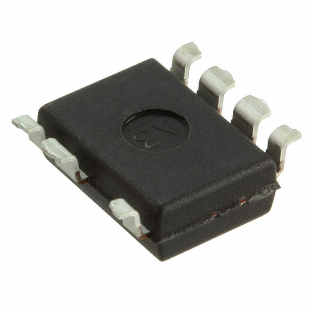
| 产品图片 | |
| rohs | 符合RoHS无铅 / 符合限制有害物质指令(RoHS)规范要求 |
| 产品系列 | 电源管理 IC,交流/直流转换器,Texas Instruments UCC28713D- |
| mouser_ship_limit | 该产品可能需要其他文件才能进口到中国。 |
| 数据手册 | |
| 产品型号 | UCC28713D |
| 产品种类 | 交流/直流转换器 |
| 供应商器件封装 | 7-SOIC |
| 其它名称 | 296-37254-5 |
| 制造商产品页 | http://www.ti.com/general/docs/suppproductinfo.tsp?distId=10&orderablePartNumber=UCC28713D |
| 功率(W) | - |
| 包装 | 管件 |
| 占空比-最大 | 42.5 % |
| 商标 | Texas Instruments |
| 安装风格 | SMD/SMT |
| 封装 | Tube |
| 封装/外壳 | 8-SOIC(0.154",3.90mm 宽)7 引线 |
| 封装/箱体 | SOIC-7 |
| 工作温度 | -40°C ~ 125°C |
| 工作温度范围 | - 40 C to + 125 C |
| 工厂包装数量 | 75 |
| 开关频率 | 600 Hz to 106 kHz |
| 拓扑结构 | Flyback |
| 标准包装 | 75 |
| 电压-击穿 | - |
| 电压-输入 | 9 V ~ 35 V |
| 电压-输出 | 14V |
| 电源电流 | 2 mA |
| 类型 | Flyback Power Supply Controller |
| 系列 | UCC28713 |
| 绝缘 | Isolated |
| 输入/电源电压—最大值 | 35 V |
| 输入/电源电压—最小值 | 9 V |
| 输出电压 | 14 V |
| 输出电流 | 25 mA |
| 输出端数量 | 1 Output |
| 输出隔离 | 隔离 |
| 频率范围 | 600Hz ~ 106kHz |


- 商务部:美国ITC正式对集成电路等产品启动337调查
- 曝三星4nm工艺存在良率问题 高通将骁龙8 Gen1或转产台积电
- 太阳诱电将投资9.5亿元在常州建新厂生产MLCC 预计2023年完工
- 英特尔发布欧洲新工厂建设计划 深化IDM 2.0 战略
- 台积电先进制程称霸业界 有大客户加持明年业绩稳了
- 达到5530亿美元!SIA预计今年全球半导体销售额将创下新高
- 英特尔拟将自动驾驶子公司Mobileye上市 估值或超500亿美元
- 三星加码芯片和SET,合并消费电子和移动部门,撤换高东真等 CEO
- 三星电子宣布重大人事变动 还合并消费电子和移动部门
- 海关总署:前11个月进口集成电路产品价值2.52万亿元 增长14.8%


PDF Datasheet 数据手册内容提取
Product Order Technical Tools & Support & Reference Folder Now Documents Software Community Design UCC28710,UCC28711,UCC28712,UCC28713 SLUSB86C–NOVEMBER2012–REVISEDJUNE2017 UCC2871x Constant-Voltage, Constant-Current Controller With Primary-Side Regulation 1 Features An internal 700-V start-up switch, dynamically- controlled operating states and a tailored modulation • <10-mWNo-LoadPower 1 profile support ultra-low standby power without • Primary-SideRegulation(PSR)EliminatesOpto- sacrificingstart-uptimeoroutputtransientresponse. Coupler Control algorithms in the UCC28710 family allow • ±5%VoltageandCurrentRegulationAcrossLine operating efficiencies to meet or exceed applicable andLoad standards. The output drive interfaces to a MOSFET • 700-VStart-UpSwitch power switch. Discontinuous conduction mode (DCM) with valley switching reduces switching losses. • 100-kHzMaximumSwitchingFrequencyEnables Modulation of switching frequency and primary High-PowerDensityChargerDesigns current peak amplitude (FM and AM) keeps the • ResonantValley-SwitchingOperationforHighest conversion efficiency high across the entire load and OverallEfficiency lineranges. • FrequencyJittertoEaseEMICompliance The controllers have a maximum switching frequency • WideVDDRangeAllowsSmallBiasCapacitor of 100 kHz and always maintain control of the peak- • ClampedGate-DriveOutputforMOSFET primary current in the transformer. Protection features help keep primary and secondary component • Overvoltage,Low-Line,andOvercurrent stresses in check. The UCC28710 allow the cable ProtectionFunctions compensation to be programmed. The UCC28711, • ProgrammableCableCompensation(UCC28710) UCC28712 and UCC28713 devices allow remote • NTCResistorInterface(UCC28711,UCC28712 temperature sensing using a negative temperature andUCC28713)withFixedCableCompensation coefficient (NTC) resistor while providing fixed cable- compensationlevels. Options • SOIC-7Package DeviceInformation(1) • CreateaCustomDesignUsingtheUCC28710 PARTNUMBER PACKAGE BODYSIZE(NOM) WiththeWEBENCH®PowerDesigner UCC28710 UCC28711 2 Applications SOIC(7) 4.91mm×3.90mm UCC28712 • USB-CompliantAdaptersandChargersfor UCC28713 ConsumerElectronics (1) For all available packages, see the orderable addendum at – SmartPhones theendofthedatasheet. – TabletComputers SimplifiedApplication – Cameras • StandbySupplyforTVandDesktop • WhiteGoods + VOUT 3 Description VAC – UCC28710 The UCC2871x family of flyback power supply controllers provides isolated-output Constant-Voltage VAUX VDD HV (CV) and Constant-Current (CC) output regulation without the use of an optical coupler. The devices VS DRV process information from the primary power switch and an auxiliary flyback winding for precise control of CBC CS outputvoltageandcurrent. GND UDG-12200 1 An IMPORTANT NOTICE at the end of this data sheet addresses availability, warranty, changes, use in safety-critical applications, intellectualpropertymattersandotherimportantdisclaimers.PRODUCTIONDATA.
UCC28710,UCC28711,UCC28712,UCC28713 SLUSB86C–NOVEMBER2012–REVISEDJUNE2017 www.ti.com Table of Contents 1 Features.................................................................. 1 8.4 DeviceFunctionalModes........................................12 2 Applications........................................................... 1 9 ApplicationandImplementation........................ 17 3 Description............................................................. 1 9.1 ApplicationInformation............................................17 4 RevisionHistory..................................................... 2 9.2 TypicalApplication..................................................17 5 DeviceComparisonTable..................................... 3 10 PowerSupplyRecommendations..................... 23 6 PinConfigurationandFunctions......................... 3 11 Layout................................................................... 23 11.1 LayoutGuidelines.................................................23 7 Specifications......................................................... 4 11.2 LayoutExample....................................................25 7.1 AbsoluteMaximumRatings......................................4 12 DeviceandDocumentationSupport................. 26 7.2 ESDRatings..............................................................4 7.3 RecommendedOperatingConditions.......................4 12.1 DeviceSupport......................................................26 7.4 ThermalInformation..................................................4 12.2 DocumentationSupport........................................28 7.5 ElectricalCharacteristics...........................................5 12.3 ReceivingNotificationofDocumentationUpdates28 7.6 TypicalCharacteristics..............................................6 12.4 CommunityResources..........................................28 12.5 Trademarks...........................................................28 8 DetailedDescription.............................................. 9 12.6 ElectrostaticDischargeCaution............................29 8.1 Overview...................................................................9 12.7 Glossary................................................................29 8.2 FunctionalBlockDiagram.........................................9 13 Mechanical,Packaging,andOrderable 8.3 FeatureDescription.................................................10 Information........................................................... 29 4 Revision History NOTE:Pagenumbersforpreviousrevisionsmaydifferfrompagenumbersinthecurrentversion. ChangesfromRevisionB(July2015)toRevisionC Page • DeletedallreferencestotheUCC28714,UCC28715,andUCC28716devices.................................................................... 1 • Deletedquasifromquasi-resonant......................................................................................................................................... 1 • AddedtheDevelopmentSupport,ReceivingNotificationofDocumentationUpdates,andCommunityResources sections................................................................................................................................................................................. 26 ChangesfromRevisionA(December2014)toRevisionB Page • UpdatedLayoutGuidelinessection...................................................................................................................................... 23 ChangesfromOriginal(November2012)toRevisionA Page • AddedPinConfigurationandFunctionssection,ESDRatingstable,FeatureDescriptionsection,DeviceFunctional Modes,ApplicationandImplementationsection,PowerSupplyRecommendationssection,Layoutsection,Device andDocumentationSupportsection,andMechanical,Packaging,andOrderableInformationsection .............................. 1 2 SubmitDocumentationFeedback Copyright©2012–2017,TexasInstrumentsIncorporated ProductFolderLinks:UCC28710 UCC28711 UCC28712 UCC28713
UCC28710,UCC28711,UCC28712,UCC28713 www.ti.com SLUSB86C–NOVEMBER2012–REVISEDJUNE2017 5 Device Comparison Table PARTNUMBER(1) MINIMUMSWITCHING OPTIONS(2) FREQUENCY UCC28710 Programmablecablecompensation UCC28711 NTCoption,0-mV(at5-Voutput)cablecompensation 680Hz UCC28712 NTCoption,150-mV(at5-Voutput)cablecompensation UCC28713 NTCoption,300-mV(at5-Voutput)cablecompensation (1) SeeMechanical,Packaging,andOrderableInformationsectionforspecificdeviceorderinginformation. (2) Forotherfixedcablecompensationoptions,callTI. 6 Pin Configuration and Functions UCC28710DPackage UCC28711,UCC28712,UCC28713DPackage 7-PinSOIC 7-PinSOIC TopView TopView VDD 1 7 HV VDD 1 7 HV VS 2 VS 2 CBC 3 6 DRV NTC 3 6 DRV GND 4 5 CS GND 4 5 CS PinFunctions PIN UCC28711 I/O DESCRIPTION NAME UCC28710 UCC28712 UCC28713 Cablecompensationisaprogrammingpinforcompensationofcablevoltagedrop.Cable CBC 3 — I compensationisprogrammedwitharesistortoGND. Currentsenseinputconnectstoaground-referencedcurrent-senseresistorinserieswith thepowerswitch.Theresultingvoltageisusedtomonitorandcontrolthepeakprimary CS 5 5 I current.Aseriesresistorcanbeaddedtothispintocompensatethepeakswitchcurrent levelsastheAC-mainsinputvaries. DriveisanoutputusedtodrivethegateofanexternalhighvoltageMOSFETswitching DRV 6 6 O transistor. Thegroundpinisboththereferencepinforthecontrollerandthelow-sidereturnforthe GND 4 4 — driveoutput.SpecialcareshouldbetakentoreturnallACdecouplingcapacitorsasclose aspossibletothispinandavoidanycommontracelengthwithanalogsignalreturnpaths. Thehigh-voltagepinconnectsdirectlytotherectifiedbulkvoltageandprovideschargeto HV 7 7 I theVDDcapacitorforstart-upofthepowersupply. NTCaninterfacetoanexternalnegativetemperaturecoefficientresistorforremote NTC — 3 I temperaturesensing.PullingthispinlowshutsdownPWMaction. VDDisthebiassupplyinputpintothecontroller.Acarefully-placedbypasscapacitorto VDD 1 1 I GNDisrequiredonthispin. Voltagesenseisaninputusedtoprovidevoltageandtimingfeedbacktothecontroller. ThispinisconnectedtoavoltagedividerbetweenanauxiliarywindingandGND.The VS 2 2 I valueoftheupperresistorofthisdividerisusedtoprogramtheAC-mainsrunandstop thresholdsandlinecompensationattheCSpin. Copyright©2012–2017,TexasInstrumentsIncorporated SubmitDocumentationFeedback 3 ProductFolderLinks:UCC28710 UCC28711 UCC28712 UCC28713
UCC28710,UCC28711,UCC28712,UCC28713 SLUSB86C–NOVEMBER2012–REVISEDJUNE2017 www.ti.com 7 Specifications 7.1 Absolute Maximum Ratings See (1). MIN MAX UNIT V Start-uppinvoltage,HV 700 V HV V Biassupplyvoltage,VDD 38 V VDD I Continuousgatecurrentsink 50 mA DRV I Continuousgatecurrentsource Self-limiting mA DRV I Peakcurrent,VS −1.2 mA VS V GatedrivevoltageatDRV −0.5 Self-limiting V DRV VS −0.75 7 V Voltage CS,CBC,NTC −0.5 5 V T Operatingjunctiontemperature −55 150 °C J Leadtemperature0.6mmfromcasefor10s 260 °C T Storagetemperature −65 150 °C stg (1) StressesbeyondthoselistedunderAbsoluteMaximumRatingsmaycausepermanentdamagetothedevice.Thesearestressratings onlyandfunctionaloperationofthedeviceattheseoranyotherconditionsbeyondthoseindicatedunderRecommendedOperating Conditionsisnotimplied.Exposuretoabsolute-maximum-ratedconditionsforextendedperiodsmayaffectdevicereliability.Allvoltages arewithrespecttoGND.Currentsarepositiveinto,negativeoutofthespecifiedterminal.Theseratingsapplyovertheoperating ambienttemperaturerangesunlessotherwisenoted. 7.2 ESD Ratings VALUE UNIT Electrostatic Human-bodymodel(HBM),perANSI/ESDA/JEDECJS-001(1) ±2000 V V (ESD) discharge Charged-devicemodel(CDM),perJEDECspecificationJESD22-C101(2) ±500 (1) JEDECdocumentJEP155statesthat500-VHBMallowssafemanufacturingwithastandardESDcontrolprocess. (2) JEDECdocumentJEP157statesthat250-VCDMallowssafemanufacturingwithastandardESDcontrolprocess.. 7.3 Recommended Operating Conditions overoperatingfree-airtemperaturerange(unlessotherwisenoted) MIN NOM MAX UNIT VDD Biassupplyoperatingvoltage 9 35 V C VDDbypasscapacitor 0.047 1 µF VDD R Cable-compensationresistance 10 kΩ CBC I VSpincurrent −1 mA VS T Operatingjunctiontemperature −40 125 °C J 7.4 Thermal Information UCC2871x THERMALMETRIC(1) D(SOIC) UNIT 7PINS R Junction-to-ambientthermalresistance 141.5 °C/W θJA R Junction-to-case(top)thermalresistance 73.8 °C/W θJC(top) R Junction-to-boardthermalresistance 89 °C/W θJB ψ Junction-to-topcharacterizationparameter 23.5 °C/W JT ψ Junction-to-boardcharacterizationparameter 88.2 °C/W JB (1) Formoreinformationabouttraditionalandnewthermalmetrics,seetheSemiconductorandICPackageThermalMetricsapplication report. 4 SubmitDocumentationFeedback Copyright©2012–2017,TexasInstrumentsIncorporated ProductFolderLinks:UCC28710 UCC28711 UCC28712 UCC28713
UCC28710,UCC28711,UCC28712,UCC28713 www.ti.com SLUSB86C–NOVEMBER2012–REVISEDJUNE2017 7.5 Electrical Characteristics overoperatingfree-airtemperaturerange,V =25V,HV=open,R =open,T =–40°Cto125°C,T =T VDD CBC(NTC) A A J (unlessotherwisenoted) PARAMETER TESTCONDITIONS MIN TYP MAX UNIT HIGH-VOLTAGESTARTUP I Start-upcurrentoutofVDD V =100V,V =0V,startstate 100 250 500 µA HV HV VDD I LeakagecurrentatHV V =400V,runstate 0.1 1 µA HVLKG HV BIASSUPPLYINPUT I Supplycurrent,run I =0,runstate 2 2.65 mA RUN DRV I Supplycurrent,wait I =0,waitstate 95 120 µA WAIT DRV I Supplycurrent,start I =0,V =18V,startstate,I =0 18 30 µA START DRV VDD HV I Supplycurrent,fault I =0,faultstate 95 125 µA FAULT DRV UNDERVOLTAGELOCKOUT V VDDturnonthreshold V lowtohigh 19 21 23 V VDD(on) VDD V VDDturnoffthreshold V hightolow 7.7 8.1 8.5 V VDD(off) VDD VSINPUT V Regulatinglevel Measuredatno-loadcondition,T =25°C(1) 4.01 4.05 4.09 V VSR J V Negativeclamplevel I =–300µA,voltsbelowground 190 250 325 mV VSNC VS I Inputbiascurrent V =4V –0.25 0 0.25 µA VSB VS CSINPUT V MaximumCSthresholdvoltage V =3.7V 738 780 810 mV CST(max) VS V MinimumCSthresholdvoltage V =4.35V 175 195 215 mV CST(min) VS K AMcontrolratio V /V 3.6 4 4.4 V/V AM CST(max) CST(min) V Constantcurrentregulatinglevel CCregulationconstant 318 330 343 mV CCR K Linecompensationcurrentratio I =–300µA,I /currentoutofCSpin 24 25 28.6 A/A LC VSLS VSLS T Leading-edgeblankingtime DRVoutputduration,V =1V 180 235 280 ns CSLEB CS DRIVERS I DRVsourcecurrent V =8V,V =9V 20 25 mA DRS DRV VDD R DRVlow-sidedriveresistance I =10mA 6 12 Ω DRVLS DRV V DRVclampvoltage V =35V 14 16 V DRCL VDD R DRVpulldowninstartstate 150 190 230 kΩ DRVSS (1) TheregulatinglevelatVSdecreaseswithtemperatureby0.8mV/˚C.Thiscompensationisincludedtoreducethepowersupplyoutput voltagevarianceovertemperature. Copyright©2012–2017,TexasInstrumentsIncorporated SubmitDocumentationFeedback 5 ProductFolderLinks:UCC28710 UCC28711 UCC28712 UCC28713
UCC28710,UCC28711,UCC28712,UCC28713 SLUSB86C–NOVEMBER2012–REVISEDJUNE2017 www.ti.com Electrical Characteristics (continued) overoperatingfree-airtemperaturerange,V =25V,HV=open,R =open,T =–40°Cto125°C,T =T VDD CBC(NTC) A A J (unlessotherwisenoted) PARAMETER TESTCONDITIONS MIN TYP MAX UNIT TIMING f Maximumswitchingfrequency V =3.7V 92 100 106 kHz SW(max) VS UCC28710 UCC28711 f Minimumswitchingfrequency V =4.35V 600 680 755 Hz SW(min) VS UCC28712 UCC28713 t Zero-crossingtimeoutdelay 1.8 2.1 2.55 µs ZTO PROTECTION V Overvoltagethreshold AtVSinput,T =25°C(1) 4.55 4.6 4.71 V OVP J V Overcurrentthreshold AtCSinput 1.4 1.5 1.6 V OCP I VSline-senseruncurrent CurrentoutofVSpinincreasing 190 225 275 µA VSL(run) I VSline-sensestopcurrent CurrentoutofVSpindecreasing 70 80 100 µA VSL(stop) K VSlinesenseratio I /I 2.45 2.8 3.05 A/A VSL VSL(run) VSL(stop) T Thermalshut-downtemperature Internaljunctiontemperature 165 °C J(stop) CABLECOMPENSATION Cablecompensationmaximum V VoltageatCBCatfullload UCC28710 2.9 3.2 3.5 V CBC(max) voltage V =open,changeinVS V CompensationatVS CBC UCC28710 –55 –15 25 mV CVS(min) regulatinglevelatfullload V =0V,changeinVSregulating V MaximumcompensationatVS CBC UCC28710 275 320 375 mV CVS(max) levelatfullload UCC28711 –55 –15 25 ChangeinVSregulatinglevelatfull V CompensationatVS UCC28712 103 mV CVS load UCC28713 206 NTCINPUT UCC28711 FaultUVLOcyclewhenbelowthis V NTCshut-downthreshold UCC28712 0.9 0.95 1 V NTCTH threshold UCC28713 UCC28711 I NTCpullupcurrent Currentoutofpin UCC28712 90 105 125 µA NTC UCC28713 7.6 Typical Characteristics VDD=25V,unlessotherwisenoted. 10 10 Run State IRUN, VDD = 25V 1 1 I - Bias Supply Current (mA) VDD 0.00.11 \/ VDWDS aTtaiutr rtS nSt-aOtateftfe /\ VDD Turn-On I - Bias Supply Current (mA) VDD 0.00.11 IISWTAAIRT,T ,V VDDDD = = 2 158VV 0.001 0.001 0.0001 0.0001 0 5 10 15 20 25 30 35 -50 -25 0 25 50 75 100 125 VDD - Bias Supply Voltage (V) TJ - Temperature (oC) C001 C002 Figure1.BiasSupplyCurrentvs.BiasSupplyVoltage Figure2.BiasSupplyCurrentvs.Temperature 6 SubmitDocumentationFeedback Copyright©2012–2017,TexasInstrumentsIncorporated ProductFolderLinks:UCC28710 UCC28711 UCC28712 UCC28713
UCC28710,UCC28711,UCC28712,UCC28713 www.ti.com SLUSB86C–NOVEMBER2012–REVISEDJUNE2017 Typical Characteristics (continued) VDD=25V,unlessotherwisenoted. 4.12 300 4.1 250 I V - VS Regulation Voltage (V) VSR34444.....90000824684 (cid:29)VS Line Sense Current (A) 112050000 IVVSSLLRSUTNO P 50 3.96 3.94 0 -50 -25 0 25 50 75 100 125 -50 -25 0 25 50 75 100 125 TJ - Temperature (oC) TJ - Temperature (oC) C003 C004 Figure3.VSRegulationVoltagevs.Temperature Figure4.VSLineSenseCurrentvs.Temperature 210 350 mV) 205 mV) 345 V - Minimum CS Threshold Voltage (CST(min)111112788990505050 V - Constant Current Regulating Level (CCR333333122334505050 170 310 -50 -25 0 25 50 75 100 125 -50 -25 0 25 50 75 100 125 TJ - Temperature (oC) TJ - Temperature (oC) C005 C006 Figure5.MinimumCSThresholdvs.Temperature Figure6.ConstantCurrentRegulatingLevelvs. Temperature 775 34 VDRV = 8 V, VVDD = 9 V 750 Hz) 32 - Minimum Switching Frequency (W(min)666677025702050505 I - DRV Source Current (mA) DRS22234680 fS 22 575 550 20 -50 -25 0 25 50 75 100 125 -50 -25 0 25 50 75 100 125 TJ - Temperature (oC) TJ - Temperature (oC) C007 C008 V =8V V =9V DRV VDD Figure7.MinimumSwitchingFrequencyvs.Temperature Figure8.DRVSourceCurrentvs.Temperature Copyright©2012–2017,TexasInstrumentsIncorporated SubmitDocumentationFeedback 7 ProductFolderLinks:UCC28710 UCC28711 UCC28712 UCC28713
UCC28710,UCC28711,UCC28712,UCC28713 SLUSB86C–NOVEMBER2012–REVISEDJUNE2017 www.ti.com Typical Characteristics (continued) VDD=25V,unlessotherwisenoted. 1.00 120 V - NTC Shutdown Threshold Voltage (V) NTCTH0000....99992468 (cid:29)I - NTC Pull-Up Current (A) NTC11110011905055 0.90 90 -50 -25 0 25 50 75 100 125 -50 -25 0 25 50 75 100 125 TJ - Temperature (oC) TJ - Temperature (oC) C009 C010 Figure9.NTCShutdownThresholdVoltagevs.Temperature Figure10.NTCPull-UpCurrentvs.Temperature 4.68 320 4.66 280 V) Over-Voltage Threshold (4444....56668024 (cid:29)V Start-Up Current (A) 112226040000 V - VS OVP4.56 I - HHV 80 4.54 40 4.52 0 -50 -25 0 25 50 75 100 125 -50 -25 0 25 50 75 100 125 TJ - Temperature (oC) TJ - Temperature (oC) C011 C012 Figure11.VSOvervoltageThresholdvs.Temperature Figure12.HVStart-UpCurrentvs.Temperature 8 SubmitDocumentationFeedback Copyright©2012–2017,TexasInstrumentsIncorporated ProductFolderLinks:UCC28710 UCC28711 UCC28712 UCC28713
UCC28710,UCC28711,UCC28712,UCC28713 www.ti.com SLUSB86C–NOVEMBER2012–REVISEDJUNE2017 8 Detailed Description 8.1 Overview The UCC2871x family is a flyback power supply controller which provides accurate voltage and constant current regulation with primary-side feedback, eliminating the need for opto-coupler feedback circuits. The controller operates in discontinuous conduction mode with valley-switching to minimize switching losses. The modulation scheme is a combination of frequency and primary peak current modulation to provide high conversion efficiency across the load range. The control law provides a wide-dynamic operating range of output power which allows thepowerdesignertoachievethe<10-mWstand-bypowerrequirement. During low-power operating ranges the device has power management features to reduce the device operating current at operating frequencies below 33 kHz. The UCC2871x family includes features in the modulator to reduce the EMI peak energy of the fundamental switching frequency and harmonics. Accurate voltage and constant current regulation, fast dynamic response, and fault protection are achieved with primary-side control. A complete charger solution can be realized with a straightforward design process, low cost and low component count. 8.2 Functional Block Diagram I HV HV OC FAULT POWER VDD 21UVVL/O8V MA&NAFGAEUMLTENT OTSVD F/ASDU LFTAULT LINE FAULT VDD GND 5V 4.05V+VCVS 25mA + CONTROL E/A VS SAMPLER LAW DRV + VCST 1/fSW 14V OV FAULT 200kΩ VALLEY VOVP S Q SWITCHING R Q + CS SECONDARY CURRENT TIMING DETECT REGULATION VCST LEB IVSLS LINE SENSE IVSLS IVSLS/KLC + 10kΩ + LINE OC FAULT FAULT 1.5V 2.2V/0.80V UCC28710/14/15 VCVS=ICBCx3kΩ UCC28711/12/13 5V CABLE 0V-VCVS(max) INTC COMPENSATION TSD/SD + FAULT ICBC 28kΩ + VNTCTH CBC NTC Copyright©2012–2017,TexasInstrumentsIncorporated SubmitDocumentationFeedback 9 ProductFolderLinks:UCC28710 UCC28711 UCC28712 UCC28713
UCC28710,UCC28711,UCC28712,UCC28713 SLUSB86C–NOVEMBER2012–REVISEDJUNE2017 www.ti.com 8.3 Feature Description 8.3.1 DetailedPinDescription 8.3.1.1 VDD(DeviceBiasVoltageSupply) The VDD pin is connected to a bypass capacitor to ground and a start-up resistance to the input bulk capacitor (+) terminal. The VDD turnon UVLO threshold is 21 V and turnoff UVLO threshold is 8.1 V, with an available operating range up to 35 V. The USB charging specification requires the output current to operate in constant- current mode from 5 V to a minimum of 2 V; this is easily achieved with a nominal VDD of approximately 25 V. The additional VDD headroom up to 35 V allows for VDD to rise due to the leakage energy delivered to the VDD capacitorinhigh-loadconditions.Also,thewideVDDrangeprovidestheadvantageofselectingarelativelysmall VDD capacitor and high-value start-up resistance to minimize no-load stand-by power loss in the start-up resistor. 8.3.1.2 GND(Ground) This is a single ground reference external to the device for the gate drive current and analog signal reference. Place the VDD bypass capacitor close to GND and VDD with short traces to minimize noise on the VS and CS signalpins. 8.3.1.3 VS(Voltage-Sense) The VS pin is connected to a resistor divider from the auxiliary winding to ground. The output-voltage feedback information is sampled at the end of the transformer secondary current demagnetization time to provide an accurate representation of the output voltage. Timing information to achieve valley-switching and to control the duty cycle of the secondary transformer current is determined by the waveform on the VS pin. Avoid placing a filtercapacitoronthisinputwhichwouldinterferewithaccuratesensingofthiswaveform. The VS pin also senses the bulk capacitor voltage to provide for AC-input run and stop thresholds, and to compensate the current-sense threshold across the AC-input range. This information is sensed during the MOSFET on-time. For the AC-input run/stop function, the run threshold on VS is 220 µA and the stop threshold is 80 µA. The values for the auxilliary voltage divider upper-resistor R and lower-resistor R can be S1 S2 determinedbytheequationsbelow. V ´ 2 R = IN(run) S1 N ´I PA VSL(run) where • N isthetransformerprimary-to-auxiliaryturnsratio, PA • V istheACRMSvoltagetoenableturnonofthecontroller(run), IN(run) • I istherun-thresholdforthecurrentpulledoutoftheVSpinduringtheMOSFETon-time.(seethe VSL(run) ElectricalCharacteristicstable) (1) R ´ V R = S1 VSR S2 N ´(V + V )- V AS OCV F VSR where • V istheconverterregulatedoutputvoltage, OCV • V istheoutputrectifierforwarddropatnear-zerocurrent, F • N isthetransformerauxiliarytosecondaryturnsratio, AS • R istheVSdividerhigh-sideresistance, S1 • V istheCVregulatinglevelattheVSinput(seetheElectricalCharacteristicstable). (2) VSR 10 SubmitDocumentationFeedback Copyright©2012–2017,TexasInstrumentsIncorporated ProductFolderLinks:UCC28710 UCC28711 UCC28712 UCC28713
UCC28710,UCC28711,UCC28712,UCC28713 www.ti.com SLUSB86C–NOVEMBER2012–REVISEDJUNE2017 Feature Description (continued) 8.3.1.4 DRV(GateDrive) The DRV pin is connected to the MOSFET gate pin, usually through a series resistor. The gate driver provides a gate-drivesignallimitedto14V.Theturnoncharacteristicofthedriverisa25-mAcurrentsourcewhichlimitsthe turnon dv/dt of the MOSFET drain and reduces the leading-edge current spike, but still provides gate-drive current to overcome the Miller plateau. The gate-drive turnoff current is determined by the low-side driver R DS(on) and any external gate-drive resistance. The user can reduce the turnoff MOSFET drain dv/dt by adding external gateresistance. 8.3.1.5 CS(CurrentSense) The current-sense pin is connected through a series resistor (R ) to the current-sense resistor (R ). The LC CS current-sense threshold is 0.75 V for I and 0.25 V for I . The series resistor R provides the function PP(max) PP(min) LC of feed-forward line compensation to eliminate change in I due to change in di/dt and the propagation delay of PP the internal comparator and MOSFET turnoff time. There is an internal leading-edge blanking time of 235 ns to eliminate sensitivity to the MOSFET turnon current spike. It should not be necessary to place a bypass capacitor on the CS pin. The value of R is determined by the target output current in constant-current (CC) regulation. CS The values of R and R can be determined by the equations below. The term η is intended to account for CS LC XFMR the energy stored in the transformer but not delivered to the secondary. This includes transformer resistance and coreloss,biaspower,andprimary-to-secondaryleakageratio. Example: With a transformer core and winding loss of 5%, primary-to-secondary leakage inductance of 3.5%, and bias power to output power ratio of 1.5%. The η value is approximately: 1 - 0.05 - 0.035 - 0.015 = 0.9. XFMR RCS = VCCR´NPS ´ hXFMR 2I OCC where • V isacurrentregulationconstant(seetheElectricalCharacteristicstable), CCR • N isthetransformerprimary-to-secondaryturnsratio(aratioof13to15isrecommendedfor5-Voutput), PS • I isthetargetoutputcurrentinconstant-currentregulation, OCC • η isthetransformerefficiency. (3) XFMR R = KLC´RS1´RCS´TD´NPA LC L P where • R istheVSpinhigh-sideresistorvalue, S1 • R isthecurrent-senseresistorvalue, CS • T isthecurrent-sensedelayincludingMOSFETturnoffdelay,add~50nstoMOSFETdelay, D • N isthetransformerprimary-to-auxiliaryturnsratio, PA • L isthetransformerprimaryinductance, P • K isacurrent-scalingconstant(seetheElectricalCharacteristicstable). (4) LC 8.3.1.6 CBC(CableCompensation),Pin1UCC28700 The cable compensation pin is connected to a resistor to ground to program the amount of output voltage compensation to offset cable resistance. The cable compensation block provides a 0-V to 3-V voltage level on the CBC pin corresponding to 0 to I output current. The resistance selected on the CBC pin programs a OCC current mirror that is summed into the VS feedback divider therefore increasing the output voltage as I OUT increases. There is an internal series resistance of 28 kΩ to the CBC pin which sets a maximum cable compensation of a 5-V output to 400 mV when CBC is shorted to ground. The CBC resistance value can be determinedbytheequationbelow. V ´3kW´(V + V ) CBC(max) OCV F R = - 28kW CBC V ´ V VSR OCBC Copyright©2012–2017,TexasInstrumentsIncorporated SubmitDocumentationFeedback 11 ProductFolderLinks:UCC28710 UCC28711 UCC28712 UCC28713
UCC28710,UCC28711,UCC28712,UCC28713 SLUSB86C–NOVEMBER2012–REVISEDJUNE2017 www.ti.com Feature Description (continued) where • V istheoutputvoltage, O • V isthediodeforwardvoltage, F • V isthetargetcablecompensationvoltageattheoutputterminals, OCBC • V isthemaximumvoltageatthecablecompensationpinatthemaximumconverteroutputcurrent(see CBC(max) theElectricalCharacteristicstable), • V istheCVregulatinglevelattheVSinput(seetheElectricalCharacteristicstable). (5) VSR 8.3.1.7 NTC(NTCThermistorShut-down),Pin1UCC28701/2/3 These versions of the UCC28700 family utilize pin 1 for an external NTC thermistor to allow user-programmable external thermal shut-down. The shut-down threshold is 0.95 V with an internal 105-µA current source which results in a 9.05-kΩ thermistor shut-down threshold. These controllers have either zero or fixed internal cable compensation. 8.3.2 FaultProtection Thereiscomprehensivefaultprotection.Protectionfunctionsinclude: • Outputovervoltagefault • Inputundervoltagefault • Internalovertemperaturefault • Primaryovercurrentfault • CSpinfault • VSpinfault AUVLOresetandrestartsequenceappliesforallfaultprotectionevents. The output overvoltage function is determined by the voltage feedback on the VS pin. If the voltage sample on VS exceeds 115% of the nominal V , the device stops switching and the internal current consumption is I OUT FAULT whichdischargestheVDDcapacitortotheUVLOturnoffthreshold.Afterthat,thedevicereturnstothestartstate andastart-upsequenceensues. The UCC2871x family always operates with cycle-by-cycle primary peak current control. The normal operating range of the CS pin is 0.78 V to 0.195 V. There is additional protection if the CS pin reaches 1.5 V. This results inaUVLOresetandrestartsequence. The line input run and stop thresholds are determined by current information at the VS pin during the MOSFET on-time. While the VS pin is clamped close to GND during the MOSFET on-time, the current through R is S1 monitored to determine a sample of the bulk capacitor voltage. A wide separation of run and stop thresholds allows clean start-up and shut-down of the power supply with the line voltage. The run current threshold is 225 µAandthestopcurrentthresholdis80 µA. The internal over-temperature protection threshold is 165°C. If the junction temperature reaches this threshold the device initiates a UVLO reset cycle. If the temperature is still high at the end of the UVLO cycle, the protectioncyclerepeats. Protection is included in the event of component failures on the VS pin. If complete loss of feedback information ontheVSpinoccurs,thecontrollerstopsswitchingandrestarts. 8.4 Device Functional Modes 8.4.1 Primary-SideVoltageRegulation Figure 13 illustrates a simplified flyback convertor with the main voltage regulation blocks of the device shown. The power train operation is the same as any DCM flyback circuit but accurate output voltage and current sensingisthekeytoprimary-sidecontrol. 12 SubmitDocumentationFeedback Copyright©2012–2017,TexasInstrumentsIncorporated ProductFolderLinks:UCC28710 UCC28711 UCC28712 UCC28713
UCC28710,UCC28711,UCC28712,UCC28713 www.ti.com SLUSB86C–NOVEMBER2012–REVISEDJUNE2017 Device Functional Modes (continued) Bulk Voltage – VBLK IS + VF– Timing VOUT Primary Secondary COUT RLOAD RS1 VS Discriminator and VCL GD DRV Sampler Control Law RS2 Minimum Period CS and Peak Primary Current RCS Zero Crossings Figure13. SimplifiedFlybackConvertor (WiththeMainVoltageRegulationBlocks) In primary-side control, the output voltage is sensed on the auxiliary winding during the transfer of transformer energy to the secondary. As shown in Figure 14 it is clear there is a down slope representing a decreasing total rectifier V and resistance voltage drop (I R ) as the secondary current decreases to zero. To achieve an F S S accurate representation of the secondary output voltage on the auxiliary winding, the discriminator reliably blocks the leakage inductance reset and ringing, continuously samples the auxiliary voltage during the down slope after the ringing is diminished, and captures the error signal at the time the secondary winding reaches zero current. The internal reference on VS is 4.05 V. Temperature compensation on the VS reference voltage of -0.8-mV/°C offsets the change in the output rectifier forward voltage with temperature. The resistor divider is selected as outlinedintheVSpindescription. VS Sample (V + V +I ´R )´N OUT F S S A N S 0 V -(V )´N BLK A N P Figure14. AuxiliaryWindingVoltage The UCC2871x family includes a VS signal sampler that signals discrimination methods to ensure an accurate sample of the output voltage from the auxiliary winding. There are however some details of the auxiliary winding signal to ensure reliable operation, specifically the reset time of the leakage inductance and the duration of any subsequent leakage inductance ring. Refer to Figure 15 below for a detailed illustration of waveform criteria to ensureareliablesampleontheVSpin.Thefirstdetailtoexamineisthedurationoftheleakageinductancereset pedestal, t in Figure 15. Because this can mimic the waveform of the secondary current decay, followed LK_RESET by a sharp downslope, it is important to keep the leakage reset time less than 600 ns for I minimum, and less PRI Copyright©2012–2017,TexasInstrumentsIncorporated SubmitDocumentationFeedback 13 ProductFolderLinks:UCC28710 UCC28711 UCC28712 UCC28713
UCC28710,UCC28711,UCC28712,UCC28713 SLUSB86C–NOVEMBER2012–REVISEDJUNE2017 www.ti.com Device Functional Modes (continued) than 2.2 µs for I maximum. The second detail is the amplitude of ringing on the V waveform following PRI AUX t . The peak-to-peak voltage at the VS pin should be less than approximately 100 mV at least 200 ns LK_RESET p-p before the end of the demagnetization time, t . If there is a concern with excessive ringing, it usually occurs DM during light or no-load conditions, when t is at the minimum. The tolerable ripple on VS is scaled up to the DM auxiliarywindingvoltagebyR andR ,andisequalto100mVx(R +R )/R . S1 S2 S1 S2 S2 t LK_RESET t SMPL VS Ring (p-p) t DM UDG-12202 Figure15. AuxiliaryWaveformDetails During voltage regulation, the controller operates in frequency modulation mode and amplitude modulation mode as illustrated in Figure 16 below. The internal operating frequency limits of the device are 100 kHz maximum and f . The transformer primary inductance and primary peak current chosen sets the maximum operating SW(min) frequency of the converter. The output preload resistor and efficiency at low power determines the converter minimumoperatingfrequency.ThereisnostabilitycompensationrequiredfortheUCC2871xfamily. ControlLawProfileinConstantVoltage(CV)Mode 100kHz I PP(max) nt) e P) urr N c MI ary / m (1 pri fSW IPP ak e f p SW ( 33kHz IPP IPP(max)/4.0 FM AM FM f SW(min) 3.3kHz 0.75V 1.3V 2.2V 3.55V 5V ControlVoltage,E/AOutput-V CL Figure16. FrequencyandAmplitudeModulationModes (DuringVoltageRegulation) 14 SubmitDocumentationFeedback Copyright©2012–2017,TexasInstrumentsIncorporated ProductFolderLinks:UCC28710 UCC28711 UCC28712 UCC28713
UCC28710,UCC28711,UCC28712,UCC28713 www.ti.com SLUSB86C–NOVEMBER2012–REVISEDJUNE2017 Device Functional Modes (continued) 8.4.2 Primary-SideCurrentRegulation TiminginformationattheVSpinandcurrentinformationattheCSpinallowaccurateregulationofthesecondary average current. The control law dictates that as power is increased in CV regulation and approaching CC regulation the primary-peak current is at I . Referring to Figure 17 below, the primary-peak current, turns PP(max) ratio, secondary demagnetization time (t ), and switching period (t ) determine the secondary average output DM SW current. Ignoring leakage inductance effects, the average output current is given by Equation 6. When the average output current reaches the regulation reference in the current control block, the controller operates in frequency modulation mode to control the output current at any output voltage at or below the voltage regulation targetaslongastheauxiliarywindingcankeepVDDabovetheUVLOturnoffthreshold. I ´N I S S PP N P t t ON DM t SW UDG-12203 Figure17. TransformerCurrents I N t I = PP ´ P ´ DM OUT 2 N t S SW (6) V 5 OCV 5.25 V 4.75 V 4 V) ge ( ±5% a olt 3 V ut p ut O 2 1 I OCC Output Current UDG-12201 Figure18. TypicalTargetOutputV-ICharacteristic 8.4.3 ValleySwitching The UCC2871x family utilizes valley switching to reduce switching losses in the MOSFET, to reduce induced- EMI, and to minimize the turnon current spike at the sense resistor. The controller operates in valley-switching in allloadconditionsunlesstheV ringinghasdiminished. DS Copyright©2012–2017,TexasInstrumentsIncorporated SubmitDocumentationFeedback 15 ProductFolderLinks:UCC28710 UCC28711 UCC28712 UCC28713
UCC28710,UCC28711,UCC28712,UCC28713 SLUSB86C–NOVEMBER2012–REVISEDJUNE2017 www.ti.com Device Functional Modes (continued) Referring to Figure 19 below, the UCC2871x family operates in a valley-skipping mode in most load conditions to maintainanaccuratevoltageorcurrentregulationpointandstillswitchonthelowestavailableV voltage. DS V DS V DRV Figure19. Valley-SkippingMode 8.4.4 Start-UpOperation The internal high-voltage start-up switch connected to the bulk capacitor voltage (V ) through the HV pin BLK charges the VDD capacitor. During start up there is typically 300 µA available to charge the VDD capacitor. WhenVDDreachesthe21-VUVLOturnonthreshold,thecontrollerisenabled,theconverterstartsswitchingand the start-up switch is turned off. The initial three cycles are limited to I . After the initial three cycles at PP(min) minimum I , the controller responds to the condition dictated by the control law. The converter will remain in PP(min) discontinuous mode during charging of the output capacitor(s), maintaining a constant output current until the outputvoltageisinregulation. 16 SubmitDocumentationFeedback Copyright©2012–2017,TexasInstrumentsIncorporated ProductFolderLinks:UCC28710 UCC28711 UCC28712 UCC28713
UCC28710,UCC28711,UCC28712,UCC28713 www.ti.com SLUSB86C–NOVEMBER2012–REVISEDJUNE2017 9 Application and Implementation NOTE Information in the following applications sections is not part of the TI component specification, and TI does not warrant its accuracy or completeness. TI’s customers are responsible for determining suitability of components for their purposes. Customers should validateandtesttheirdesignimplementationtoconfirmsystemfunctionality. 9.1 Application Information The UCC2871x family of flyback power supply controllers provides constant voltage (CV) and constant current (CC) output regulation to help meet USB-compliant adaptors and charger requirements. These devices use the information obtained from auxiliary winding sensing (VS) to control the output voltage and do not require optocoupler/TL431 feedback circuitry. Eliminating the optocoupler feedback reduces component count and makesthedesignmorecosteffective.RefertoFigure20fordetails. 9.2 Typical Application The procedure in the Detailed Design Procedure section outlines the steps to design a constant-voltage, constant-current flyback converter using the UCC2871x family of controllers. Refer to the typical application schematicforcomponentlocation(Figure20)andtheDeviceNomenclature sectionforvariabledefinitions. VBLK + VF - + CB1 CB2 Np Ns COUT RPL VOUT – VAC UCC28710 SOIC-7 VAUX + VFA - VDD HV Na RS1 CDD DRV VS CS RS2 CBC RLC RCS RCBC GND Figure20. DesignProcedureApplicationExample 9.2.1 DesignRequirements Table1.DesignParameters PARAMETER NOTESANDCONDITIONS MIN NOM MAX UNIT INPUTCHARACTERISTICS V InputVoltage 100 115/230 240 V IN f LineFrequency 47 50/60 64 Hz LINE P NoLoadInputPower V =Nom,I =0A 10 mW SB_CONV IN O V BrownoutVoltage I =Nom 70 V IN(RUN) O OUTPUTCHARACTERISTICS V OutputVoltage V =Nom,I =Nom 4.75 5 5.25 V O IN O V OutputVoltageRipple V =Nom,I =Max 0.1 V RIPPLE IN O I OutputCurrent V =MintoMax 1 1.05 A O IN Copyright©2012–2017,TexasInstrumentsIncorporated SubmitDocumentationFeedback 17 ProductFolderLinks:UCC28710 UCC28711 UCC28712 UCC28713
UCC28710,UCC28711,UCC28712,UCC28713 SLUSB86C–NOVEMBER2012–REVISEDJUNE2017 www.ti.com Typical Application (continued) Table1.DesignParameters(continued) PARAMETER NOTESANDCONDITIONS MIN NOM MAX UNIT V OutputOVP I =MintoMax 5.75 V OVP OUT TransientResponse (0.1to0.6A)or(0.6to0.1A) V LoadStep(V =4.1Vto6V) V =0.9VforC calculation 4.1 5 6 A OΔ O OΔ OUT inapplicationssection SYSTEMSCHARACTERISTICS SwitchingFrequency 90 kHz FullLoadEfficiency(115/230VRMS η I =1A 74% 76% Input) O 9.2.2 DetailedDesignProcedure 9.2.2.1 CustomDesignWithWEBENCH® Tools ClickheretocreateacustomdesignusingtheUCC28710devicewiththeWEBENCH®PowerDesigner. 1. Startbyenteringtheinputvoltage(V ),outputvoltage(V ),andoutputcurrent(I )requirements. IN OUT OUT 2. Optimizethedesignforkeyparameterssuchasefficiency,footprint,andcostusingtheoptimizerdial. 3. ComparethegenerateddesignwithotherpossiblesolutionsfromTexasInstruments. The WEBENCH Power Designer provides a customized schematic along with a list of materials with real-time pricingandcomponentavailability. Inmostcases,theseactionsareavailable: • Runelectricalsimulationstoseeimportantwaveformsandcircuitperformance • Runthermalsimulationstounderstandboardthermalperformance • ExportcustomizedschematicandlayoutintopopularCADformats • PrintPDFreportsforthedesign,andsharethedesignwithcolleagues GetmoreinformationaboutWEBENCHtoolsatwww.ti.com/WEBENCH. 9.2.2.2 Stand-byPowerEstimate Assuming no-load stand-by power is a critical design parameter, determine estimated no-load power based on targetconvertermaximumswitchingfrequencyandoutputpowerrating. Thefollowingequationestimatesthestand-bypoweroftheconverter. P ´f P = OUT MIN SB_CONV h ´K 2 ´f SB AM MAX (7) For a typical USB charger application, the bias power during no-load is approximately 2.5 mW. This is based on 25-V VDD and 100-µA bias current. The output preload resistor can be estimated by V and the difference in OCV the converter stand-by power and the bias power. The equation for output preload resistance accounts for bias powerestimatedat2.5mW. V 2 R = OCV PL P - 2.5mW SB_CONV (8) The capacitor bulk voltage for the loss estimation is the highest voltage for the stand-by power measurement, typically325V . DC For the total stand-by power estimation add an estimated 2.5 mW for snubber loss to the converter stand-by powerloss. P =P +2.5mW SB SB_CONV (9) 18 SubmitDocumentationFeedback Copyright©2012–2017,TexasInstrumentsIncorporated ProductFolderLinks:UCC28710 UCC28711 UCC28712 UCC28713
UCC28710,UCC28711,UCC28712,UCC28713 www.ti.com SLUSB86C–NOVEMBER2012–REVISEDJUNE2017 9.2.2.3 InputBulkCapacitanceandMinimumBulkVoltage Determine the minimum voltage on the input capacitance, C and C total, in order to determine the maximum B1 B2 Np to Ns turns ratio of the transformer. The input power of the converter based on target full-load efficiency, minimum input RMS voltage, and minimum AC input frequency are used to determine the input capacitance requirement. MaximuminputpowerisdeterminedbasedonV ,I ,andthefull-loadefficiencytarget. OCV OCC V ´I P = OCV OCC IN h (10) The below equation provides an accurate solution for input capacitance based on a target minimum bulk capacitorvoltage.Totargetagiveninputcapacitancevalue,iteratetheminimumcapacitorvoltagetoachievethe targetcapacitance. 2P ´æç0.25 + 1 ´arcsinæç VBULK(min) ö÷ö÷ IN ç 2P ç 2 ´ V ÷÷ è è IN(min) øø C = BULK (2V 2 - V 2)´f IN(min) BULK(min) LINE (11) 9.2.2.4 TransformerTurnsRatio,Inductance,Primary-PeakCurrent Themaximumprimary-to-secondaryturnsratiocanbedeterminedbythetargetmaximumswitchingfrequencyat fullload,theminimuminputcapacitorbulkvoltage,andtheestimatedDCMresonanttime. Initiallydeterminethemaximumavailabletotaldutycycleoftheontimeandsecondaryconductiontimebasedon target switching frequency and DCM resonant time. For DCM resonant time, assume 500 kHz if you do not have an estimate from previous designs. For the transition mode operation limit, the period required from the end of secondary current conduction to the first valley of the V voltage is ½ of the DCM resonant period, or 1 µs DS assuming500-kHzresonantfrequency.D canbedeterminedusingtheequationbelow. MAX æt ö DMAX =1-ç R ´fMAX÷-DMAGCC è 2 ø (12) Once D is known, the maximum turns ratio of the primary to secondary can be determined with the equation MAX below. D is defined as the secondary diode conduction duty cycle during constant-current, CC, operation. It MAGCC is set internally by the UCC2871x family at 0.425. The total voltage on the secondary winding needs to be determined; which is the sum of V , the secondary rectifier V , and the cable compensation voltage (V ). OCV F OCBC Forthe5-VUSBchargerapplications,aturnsratiorangeof13to15istypicallyused. D ´ V MAX BULK(min) N = PS(max) D ´(V + V + V ) MAGCC OCV F OCBC (13) Once an optimum turns ratio is determined from a detailed transformer design, use this ratio for the following parameters. The UCC2871x family constant-current regulation is achieved by maintaining a maximum D duty cycle of MAG 0.425 at the maximum primary current setting. The transformer turns ratio and constant-current regulating voltagedeterminethecurrentsenseresistorforatargetconstantcurrent. Since not all of the energy stored in the transformer is transferred to the secondary, a transformer efficiency term is included. This efficiency number includes the core and winding losses, leakage inductance ratio, and bias power ratio to rated output power. For a 5-V, 1-A charger example, bias power of 1.5% is a good estimate. An overall transformer efficiency of 0.9 is a good estimate to include 3.5% leakage inductance, 5% core and winding loss,and1.5%biaspower. RCS = VCCR´NPS ´ hXFMR 2I OCC (14) The primary transformer inductance can be calculated using the standard energy storage equation for flyback transformers. Primary current, maximum switching frequency and output and transformer power losses are includedintheequationbelow.Initiallydeterminetransformerprimarycurrent. Primarycurrentissimplythemaximumcurrentsensethresholddividedbythecurrentsenseresistance. Copyright©2012–2017,TexasInstrumentsIncorporated SubmitDocumentationFeedback 19 ProductFolderLinks:UCC28710 UCC28711 UCC28712 UCC28713
UCC28710,UCC28711,UCC28712,UCC28713 SLUSB86C–NOVEMBER2012–REVISEDJUNE2017 www.ti.com V I = CST(max) PP(max) R CS (15) 2(V + V + V )´I OCV F OCBC OCC L = P h ´I 2 ´f XFMR PP(max) MAX (16) The secondary winding to auxiliary winding transformer turns ratio (N ) is determined by the lowest target AS operating output voltage in constant-current regulation and the VDD UVLO of the UCC2871x family. There is additional energy supplied to VDD from the transformer leakage inductance energy which allows a lower turns ratiotobeusedinmanydesigns. V + V N = DD(off) FA AS V + V OCC F (17) 9.2.2.5 TransformerParameterVerification The transformer turns ratio selected affects the MOSFET V and secondary rectifier reverse voltage so these DS should be reviewed. The UCC2871x family does require a minimum on time of the MOSFET (t ) and minimum ON D time (t ) of the secondary rectifier in the high line, minimum load condition. The selection of f , L MAG DMAG MAX P andR affectstheminimumt andt . CS ON DMAG ThesecondaryrectifierandMOSFETvoltagestresscanbedeterminedbytheequationsbelow. V ´ 2 V = IN(max) + V + V REV OCV OCBC N PS (18) FortheMOSFETV voltagestress,anestimatedleakageinductancevoltagespike(V )needstobeincluded. DS LK V (cid:11)V u 2(cid:12)(cid:14)(cid:11)V (cid:14)V (cid:14)V (cid:12)uN (cid:14)V DSPK IN(max) OCV F OCBC PS LK (19) Equation 20 and Equation 21 are used to determine if the minimum t target of 300 ns and minimum t ON DMAG targetof1.2 µsisachieved. t = LP ´IPP(max)´VCST(min) ON(min) VIN(max)´ 2 VCST(max) (20) tON´VIN(max)´ 2 t = DMAG(min) NPS´(VOCV +VF) (21) 9.2.2.6 OutputCapacitance The output capacitance value is typically determined by the transient response requirement from no-load. For example, in some USB charger applications there is a requirement to maintain a minimum V of 4.1 V with a O load-step transient of 0 mA to 500 mA . The equation below assumes that the switching frequency can be at the UCC2871xfamily'sminimumoff . SW(min) æ 1 ö I ç +150ms÷ TRANçf ÷ è SW(min) ø C = OUT V OD (22) Another consideration of the output capacitor(s) is the ripple voltage requirement which is reviewed based on secondary peak current and ESR. A margin of 20% is added to the capacitor ESR requirement in the equation below. V ´0.8 R = RIPPLE ESR I ´N PP(max) PS (23) 20 SubmitDocumentationFeedback Copyright©2012–2017,TexasInstrumentsIncorporated ProductFolderLinks:UCC28710 UCC28711 UCC28712 UCC28713
UCC28710,UCC28711,UCC28712,UCC28713 www.ti.com SLUSB86C–NOVEMBER2012–REVISEDJUNE2017 9.2.2.7 VDDCapacitance,C DD The capacitance on VDD needs to supply the device operating current until the output of the converter reaches the target minimum operating voltage in constant-current regulation. At this time the auxiliary winding can sustain the voltage to the UCC2871x family. The total output current available to the load and to charge the output capacitors is the constant-current regulation target. The equation below assumes the output current of the flyback is available to charge the output capacitance until the minimum output voltage is achieved. There is an estimated1mAofgate-drivecurrentintheequationand1VofmarginaddedtoVDD. C ´V (I +1mA)´ OUT OCC RUN I C = OCC DD ( ) V -V -1V DD(on) DD(off) (24) 9.2.2.8 VSResistorDivider,LineCompensation,andCableCompensation The VS divider resistors determine the output voltage regulation point of the flyback converter, also the high-side divider resistor (R ) determines the line voltage at which the controller enables continuous DRV operation. R S1 S1 is initially determined based on transformer auxiliary to primary turns ratio and desired input voltage operating threshold. V ´ 2 R = IN(run) S1 N ´I PA VSL(run) (25) Thelow-sideVSpinresistorisselectedbasedondesiredV regulationvoltage. O R ´ V R = S1 VSR S2 N ´(V + V )- V AS OCV F VSR (26) The UCC2871x family can maintain tight constant-current regulation over input line by utilizing the line compensation feature. The line compensation resistor (R ) value is determined by current flowing in R and LC S1 expectedgatedriveandMOSFETturnoffdelay.Assumea50-nsinternaldelayintheUCC2871xfamily. K ´R ´R ´t ´N R = LC S1 CS D PA LC L P (27) On the UCC28710, which has adjustable cable compensation, the resistance for the desired compensation level attheoutputterminalscanbedeterminedusingEquation28. V ´3kW´(V + V ) CBC(max) OCV F R = - 28kW CBC V ´ V VSR OCBC (28) 9.2.3 ApplicationCurves 78% 76% 74% cy 72% n e ci Effi 70% 68% 66% Efficiency at 115 VRMS Efficiency at 230 VRMS 64% 10% 20% 30% 40% 50% 60% 70% 80% 90% 100% Output Power D001 Figure21.Efficiency Figure22.OutputatStartupat115-VRMS (NoLoad) Copyright©2012–2017,TexasInstrumentsIncorporated SubmitDocumentationFeedback 21 ProductFolderLinks:UCC28710 UCC28711 UCC28712 UCC28713
UCC28710,UCC28711,UCC28712,UCC28713 SLUSB86C–NOVEMBER2012–REVISEDJUNE2017 www.ti.com Figure23.OutputatStartupat115-VRMS Figure24.OutputatStartupat230-VRMS (5-ΩLoad) (NoLoad) CH1=I ,CH4=V Witha5-VOffset O O Figure25.OutputatStartupat230-VRMS Figure26.LoadTransients: (5-ΩLoad) (0.1-Ato0.6-ALoadStep) CH1=I ,CH4=V Witha5-VOffset O O CH4=V ,OutputvoltageatEVMoutput O CH2=V ,Outputvoltagemeasuredattheendofthe3Mof O cableinparallelwitha1-uFcapacitor.Theoutputvoltagehas lessthan50mVofoutputrippleattheendofthecable. Figure27.LoadTransients: Figure28.OutputRippleVoltageatFullLoad (0.6-Ato0.1-ALoadStep) 22 SubmitDocumentationFeedback Copyright©2012–2017,TexasInstrumentsIncorporated ProductFolderLinks:UCC28710 UCC28711 UCC28712 UCC28713
UCC28710,UCC28711,UCC28712,UCC28713 www.ti.com SLUSB86C–NOVEMBER2012–REVISEDJUNE2017 10 Power Supply Recommendations TheUCC2871xfamilyisintendedforAC/DCadaptersandchargerswithinputvoltagerangeof85V to265 AC(rms) V using Flyback topology. It can be used in other applications and converter topologies with different input AC(rms) voltages. Be sure that all voltages and currents are within the recommended operating conditions and absolute maximum ratings of the device. To maintain output current regulation over the entire input voltage range, design the converter to operate close to f when in full-load conditions. To improve thermal performance increase the MAX copperareaconnectedtoGNDpins. 11 Layout 11.1 Layout Guidelines • High frequency bypass Capacitor C5 should be placed across Pin 1 and 4 as close as you can get it to the pins. • Resistor R4 and C5 form a low pass filter and the connection of R4 and C5 should be as close to the VDD pinaspossible. • The VS pin controls the output voltage through the transformer turns ratio and the voltage divider of R5 and R11. Note the trace length between the R5, R11 and VS pin should be as short as possible to reduce or eliminatepossibleEMIcoupling. • Note the IC ground and power ground should meet at the bulk capacitor’s (C6 and C7) return. Try to ensure thathighfrequency/highcurrentfromthepowerstagedoesnotgothroughthesignalground. – The high frequency/high current path that you need to be cautious of on the primary is C7 +, T1 (P5, P3), Q1d,Q1s,R8tothereturnofC6andC7.Trytokeepallhighcurrentloopsasshortaspossible. • Trytokeepallhighcurrentloopsasshortaspossible. • Keepallhighcurrent/highfrequencytracesawayfromorperpendiculartoothertracesinthedesign. • TracesonthevoltageclampformedbyD1,R2,D3andC2asshortaspossible. • C6 return needs to be as close to the bulk capacitor supply as possible. This reduces the magnitude of dv/dt causedbylargedi/dt. • Avoidmountingsemiconductorsundermagnetics. Copyright©2012–2017,TexasInstrumentsIncorporated SubmitDocumentationFeedback 23 ProductFolderLinks:UCC28710 UCC28711 UCC28712 UCC28713
UCC28710,UCC28711,UCC28712,UCC28713 SLUSB86C–NOVEMBER2012–REVISEDJUNE2017 www.ti.com C1 R1 T1 7508110127REV01 R2 D1 3 1Dn2F 39 TP1 VOUT + 4 9 C2 D3 649 MURS160-13-F J1 1nF SMBJP6KE82A 51 7 B340LB-13-F+ C3 + C4 R3 Vout = 5V/1A 560 uF 560 uF 15.4k 2 VOUT - TP2 Q1 D4 L1 STD2HNK70Z-1 JP1 RS1B-13-F 1 2 R4 470 uH R825.5k 22.5 UCC2U81711D VIN = 90V to 256V RMS D5 1 VDD TP3 2 VS HV8 R9 + C6 + C7 3 CBC/NTC DRV 6 Line 1 R6 R7 R8 CS 5 2 10 ohm Fusible Resistor 4.7 uF 4.7 uF 10 10.0k 1.96 4 GND R10 Neutral 3 R11 100k R12 J2 27.4k C5 1.00k TP4 HD06 330nF Copyright © 2017,Texas Instruments Incorporated Novaluemeansnotpopulated. Figure29. 5-WUSBAdapterSchematic 24 SubmitDocumentationFeedback Copyright©2012–2017,TexasInstrumentsIncorporated ProductFolderLinks:UCC28710 UCC28711 UCC28712 UCC28713
UCC28710,UCC28711,UCC28712,UCC28713 www.ti.com SLUSB86C–NOVEMBER2012–REVISEDJUNE2017 11.2 Layout Example VOUT+ TP1 NEUTRAL R11 R5 T1 R1 TP4 R10 R4 D4 J1 1 1 5 C C4 C U1 7 TP2 D5 R VOUT- D2 J2 D1 R9 P1 1 R6 J Q R12 R8 C2 R2 C3 TP3 LINE C6 C7 L1 D3 Figure30. LayoutExampleSchematic Copyright©2012–2017,TexasInstrumentsIncorporated SubmitDocumentationFeedback 25 ProductFolderLinks:UCC28710 UCC28711 UCC28712 UCC28713
UCC28710,UCC28711,UCC28712,UCC28713 SLUSB86C–NOVEMBER2012–REVISEDJUNE2017 www.ti.com 12 Device and Documentation Support 12.1 Device Support 12.1.1 DevelopmentSupport For design tools see the UCC2871x Calculator, UCC2871x PSpice Transient Model, UCC2871x TINA-TI TransientSpiceModel,andUCC2871xTINA-TITransientReferenceDesign. 12.1.1.1 CustomDesignWithWEBENCH® Tools ClickheretocreateacustomdesignusingtheUCC28710devicewiththeWEBENCH®PowerDesigner. 1. Startbyenteringtheinputvoltage(V ),outputvoltage(V ),andoutputcurrent(I )requirements. IN OUT OUT 2. Optimizethedesignforkeyparameterssuchasefficiency,footprint,andcostusingtheoptimizerdial. 3. ComparethegenerateddesignwithotherpossiblesolutionsfromTexasInstruments. The WEBENCH Power Designer provides a customized schematic along with a list of materials with real-time pricingandcomponentavailability. Inmostcases,theseactionsareavailable: • Runelectricalsimulationstoseeimportantwaveformsandcircuitperformance • Runthermalsimulationstounderstandboardthermalperformance • ExportcustomizedschematicandlayoutintopopularCADformats • PrintPDFreportsforthedesign,andsharethedesignwithcolleagues GetmoreinformationaboutWEBENCHtoolsatwww.ti.com/WEBENCH. 12.1.2 DeviceNomenclature 12.1.2.1 CapacitanceTermsinFarads • C :totalinputcapacitanceofC andC . BULK B1 B2 • C :minimumrequiredcapacitanceontheVDDpin. DD • C :minimumoutputcapacitancerequired. OUT 12.1.2.2 DutyCycleTerms • D :secondarydiodeconductiondutycycleinCC,0.425. MAGCC • D :MOSFETon-timedutycycle. MAX 12.1.2.3 FrequencyTermsinHertz • f :minimumlinefrequency. LINE • f :targetfull-loadmaximumswitchingfrequencyoftheconverter. MAX • f :minimumswitchingfrequencyoftheconverter,add15%marginoverthef limitofthedevice. MIN SW(min) • f :minimumswitchingfrequency(seeElectricalCharacteristics). SW(min) 12.1.2.4 CurrentTermsinAmperes • I :converteroutputconstant-currenttarget. OCC • I :maximumtransformerprimarycurrent. PP(max) • I :start-upbiassupplycurrent(seeElectricalCharacteristics). START • I :requiredpositiveload-stepcurrent. TRAN • I :VSpinruncurrent(seeElectricalCharacteristics). VSL(run) 12.1.2.5 CurrentandVoltageScalingTerms • K :maximum-to-minimumpeakprimarycurrentratio(seeElectricalCharacteristics). AM • K :current-scalingconstant(seeElectricalCharacteristics). LC 26 SubmitDocumentationFeedback Copyright©2012–2017,TexasInstrumentsIncorporated ProductFolderLinks:UCC28710 UCC28711 UCC28712 UCC28713
UCC28710,UCC28711,UCC28712,UCC28713 www.ti.com SLUSB86C–NOVEMBER2012–REVISEDJUNE2017 Device Support (continued) 12.1.2.6 TransformerTerms • L :transformerprimaryinductance. P • N :transformerauxiliary-to-secondaryturnsratio. AS • N :transformerprimary-to-auxiliaryturnsratio. PA • N :transformerprimary-to-secondaryturnsratio. PS 12.1.2.7 PowerTermsinWatts • P :convertermaximuminputpower. IN • P :full-loadoutputpoweroftheconverter. OUT • P :VDDstart-upresistorpowerdissipation. RSTR • P :totalstand-bypower. SB • P :P minusstart-upresistorandsnubberlosses. SB_CONV SB 12.1.2.8 ResistanceTermsin Ω • R :primarycurrentprogrammingresistance. CS • R :totalESRoftheoutputcapacitor(s). ESR • R :preloadresistanceontheoutputoftheconverter. PL • R :high-sideVSpinresistance. S1 • R :low-sideVSpinresistance. S2 12.1.2.9 TimingTermsinSeconds • t :current-sensedelayincludingMOSFETturn-offdelay;add50nstoMOSFETdelay. D • t :minimumsecondaryrectifierconductiontime. DMAG(min) • t :minimumMOSFETontime. ON(min) • t :resonantfrequencyduringtheDCM(discontinuousconductionmode)time. R 12.1.2.10 VoltageTermsinVolts • V :highestbulkcapacitorvoltageforstand-bypowermeasurement. BLK • V :minimumvoltageonC andC atfullpower. BULK(min) B1 B2 • V :targetcablecompensationvoltageattheoutputterminals. OCBC • V : maximum voltage at the CBC pin at the maximum converter output current (see Electrical CBC(max) Characteristics). • V :constant-currentregulatingvoltage(seeElectricalCharacteristics). CCR • V :CSpinmaximumcurrent-sensethreshold(seeElectricalCharacteristics). CST(max) • V :CSpinminimumcurrent-sensethreshold(seeElectricalCharacteristics). CST(min) • V :UVLOturn-offvoltage(seeElectricalCharacteristics). DD(off) • V :UVLOturn-onvoltage(seeElectricalCharacteristics). DD(on) • V :outputvoltagedropallowedduringtheload-steptransient. OΔ • V :peakMOSFETdrain-to-sourcevoltageathighline. DSPK • V :secondaryrectifierforwardvoltagedropatnear-zerocurrent. F • V :auxiliaryrectifierforwardvoltagedrop. FA • V :estimatedleakageinductanceenergyresetvoltage. LK • V :regulatedoutputvoltageoftheconverter. OCV • V :targetlowestconverteroutputvoltageinconstant-currentregulation. OCC • V :peakreversevoltageonthesecondaryrectifier. REV • V :outputpeak-to-peakripplevoltageatfull-load. RIPPLE • V :CVregulatinglevelattheVSinput(seeElectricalCharacteristics). VSR 12.1.2.11 ACVoltageTermsinV RMS • V :maximuminputvoltagetotheconverter. IN(max) Copyright©2012–2017,TexasInstrumentsIncorporated SubmitDocumentationFeedback 27 ProductFolderLinks:UCC28710 UCC28711 UCC28712 UCC28713
UCC28710,UCC28711,UCC28712,UCC28713 SLUSB86C–NOVEMBER2012–REVISEDJUNE2017 www.ti.com Device Support (continued) • V :minimuminputvoltagetotheconverter. IN(min) • V :converterinputstart-up(run)voltage. IN(run) 12.1.2.12 EfficiencyTerms • η :estimatedefficiencyoftheconverteratno-loadcondition,notincludingstart-upresistanceorbiaslosses. SB Fora5-VUSBchargerapplication,60%to65%isagoodinitialestimate. • η:converteroverallefficiency. • η :transformerprimary-to-secondarypowertransferefficiency. XFMR 12.2 Documentation Support 12.2.1 RelatedDocumentation Forrelateddocumentationseethefollowing: • ChoosingStandardRecoveryDiodeorUltra-FastDiodeinSnubber • ControlChallengesforLowPowerAC/DCConverters • TroubleshootingTIPSRControllers • UsingtheUCC28711EVM-160,EvaluationModule • LeakageCurrentMeasurementReferenceDesignforDeterminingInsulationResistance • 100-V/200-VACInput30-WFlybackIsolatedPowerSupplyReferenceDesignforServoDrives 12.2.2 RelatedLinks The table below lists quick access links. Categories include technical documents, support and community resources,toolsandsoftware,andquickaccesstosampleorbuy. Table2.RelatedLinks TECHNICAL TOOLS& SUPPORT& PARTS PRODUCTFOLDER ORDERNOW DOCUMENTS SOFTWARE COMMUNITY UCC28710 Clickhere Clickhere Clickhere Clickhere Clickhere UCC28711 Clickhere Clickhere Clickhere Clickhere Clickhere UCC28712 Clickhere Clickhere Clickhere Clickhere Clickhere UCC28713 Clickhere Clickhere Clickhere Clickhere Clickhere 12.3 Receiving Notification of Documentation Updates To receive notification of documentation updates, navigate to the device product folder on ti.com. In the upper right corner, click on Alert me to register and receive a weekly digest of any product information that has changed.Forchangedetails,reviewtherevisionhistoryincludedinanyreviseddocument. 12.4 Community Resources The following links connect to TI community resources. Linked contents are provided "AS IS" by the respective contributors. They do not constitute TI specifications and do not necessarily reflect TI's views; see TI's Terms of Use. TIE2E™OnlineCommunity TI'sEngineer-to-Engineer(E2E)Community.Createdtofostercollaboration amongengineers.Ate2e.ti.com,youcanaskquestions,shareknowledge,exploreideasandhelp solveproblemswithfellowengineers. DesignSupport TI'sDesignSupport QuicklyfindhelpfulE2Eforumsalongwithdesignsupporttoolsand contactinformationfortechnicalsupport. 12.5 Trademarks E2EisatrademarkofTexasInstruments. WEBENCHisaregisteredtrademarkofTexasInstruments. Allothertrademarksarethepropertyoftheirrespectiveowners. 28 SubmitDocumentationFeedback Copyright©2012–2017,TexasInstrumentsIncorporated ProductFolderLinks:UCC28710 UCC28711 UCC28712 UCC28713
UCC28710,UCC28711,UCC28712,UCC28713 www.ti.com SLUSB86C–NOVEMBER2012–REVISEDJUNE2017 12.6 Electrostatic Discharge Caution Thesedeviceshavelimitedbuilt-inESDprotection.Theleadsshouldbeshortedtogetherorthedeviceplacedinconductivefoam duringstorageorhandlingtopreventelectrostaticdamagetotheMOSgates. 12.7 Glossary SLYZ022—TIGlossary. Thisglossarylistsandexplainsterms,acronyms,anddefinitions. 13 Mechanical, Packaging, and Orderable Information The following pages include mechanical, packaging, and orderable information. This information is the most current data available for the designated devices. This data is subject to change without notice and revision of thisdocument.Forbrowser-basedversionsofthisdatasheet,refertotheleft-handnavigation. Copyright©2012–2017,TexasInstrumentsIncorporated SubmitDocumentationFeedback 29 ProductFolderLinks:UCC28710 UCC28711 UCC28712 UCC28713
PACKAGE OPTION ADDENDUM www.ti.com 6-Feb-2020 PACKAGING INFORMATION Orderable Device Status Package Type Package Pins Package Eco Plan Lead/Ball Finish MSL Peak Temp Op Temp (°C) Device Marking Samples (1) Drawing Qty (2) (6) (3) (4/5) UCC28710D ACTIVE SOIC D 7 75 Green (RoHS NIPDAU Level-1-260C-UNLIM -40 to 125 U28710 & no Sb/Br) UCC28710DR ACTIVE SOIC D 7 2500 Green (RoHS NIPDAU Level-1-260C-UNLIM -40 to 125 U28710 & no Sb/Br) UCC28711D ACTIVE SOIC D 7 75 Green (RoHS NIPDAU Level-1-260C-UNLIM -40 to 125 U28711 & no Sb/Br) UCC28711DR ACTIVE SOIC D 7 2500 Green (RoHS NIPDAU Level-1-260C-UNLIM -40 to 125 U28711 & no Sb/Br) UCC28712D ACTIVE SOIC D 7 75 Green (RoHS NIPDAU Level-1-260C-UNLIM -40 to 125 U28712 & no Sb/Br) UCC28712DR ACTIVE SOIC D 7 2500 Green (RoHS NIPDAU Level-1-260C-UNLIM -40 to 125 U28712 & no Sb/Br) UCC28713D ACTIVE SOIC D 7 75 Green (RoHS NIPDAU Level-1-260C-UNLIM -40 to 125 U28713 & no Sb/Br) UCC28713DR ACTIVE SOIC D 7 2500 Green (RoHS NIPDAU Level-1-260C-UNLIM -40 to 125 U28713 & no Sb/Br) (1) The marketing status values are defined as follows: ACTIVE: Product device recommended for new designs. LIFEBUY: TI has announced that the device will be discontinued, and a lifetime-buy period is in effect. NRND: Not recommended for new designs. Device is in production to support existing customers, but TI does not recommend using this part in a new design. PREVIEW: Device has been announced but is not in production. Samples may or may not be available. OBSOLETE: TI has discontinued the production of the device. (2) RoHS: TI defines "RoHS" to mean semiconductor products that are compliant with the current EU RoHS requirements for all 10 RoHS substances, including the requirement that RoHS substance do not exceed 0.1% by weight in homogeneous materials. Where designed to be soldered at high temperatures, "RoHS" products are suitable for use in specified lead-free processes. TI may reference these types of products as "Pb-Free". RoHS Exempt: TI defines "RoHS Exempt" to mean products that contain lead but are compliant with EU RoHS pursuant to a specific EU RoHS exemption. Green: TI defines "Green" to mean the content of Chlorine (Cl) and Bromine (Br) based flame retardants meet JS709B low halogen requirements of <=1000ppm threshold. Antimony trioxide based flame retardants must also meet the <=1000ppm threshold requirement. (3) MSL, Peak Temp. - The Moisture Sensitivity Level rating according to the JEDEC industry standard classifications, and peak solder temperature. (4) There may be additional marking, which relates to the logo, the lot trace code information, or the environmental category on the device. Addendum-Page 1
PACKAGE OPTION ADDENDUM www.ti.com 6-Feb-2020 (5) Multiple Device Markings will be inside parentheses. Only one Device Marking contained in parentheses and separated by a "~" will appear on a device. If a line is indented then it is a continuation of the previous line and the two combined represent the entire Device Marking for that device. (6) Lead/Ball Finish - Orderable Devices may have multiple material finish options. Finish options are separated by a vertical ruled line. Lead/Ball Finish values may wrap to two lines if the finish value exceeds the maximum column width. Important Information and Disclaimer:The information provided on this page represents TI's knowledge and belief as of the date that it is provided. TI bases its knowledge and belief on information provided by third parties, and makes no representation or warranty as to the accuracy of such information. Efforts are underway to better integrate information from third parties. TI has taken and continues to take reasonable steps to provide representative and accurate information but may not have conducted destructive testing or chemical analysis on incoming materials and chemicals. TI and TI suppliers consider certain information to be proprietary, and thus CAS numbers and other limited information may not be available for release. In no event shall TI's liability arising out of such information exceed the total purchase price of the TI part(s) at issue in this document sold by TI to Customer on an annual basis. Addendum-Page 2
PACKAGE MATERIALS INFORMATION www.ti.com 30-May-2017 TAPE AND REEL INFORMATION *Alldimensionsarenominal Device Package Package Pins SPQ Reel Reel A0 B0 K0 P1 W Pin1 Type Drawing Diameter Width (mm) (mm) (mm) (mm) (mm) Quadrant (mm) W1(mm) UCC28710DR SOIC D 7 2500 330.0 12.4 6.4 5.2 2.1 8.0 12.0 Q1 UCC28711DR SOIC D 7 2500 330.0 12.4 6.4 5.2 2.1 8.0 12.0 Q1 UCC28712DR SOIC D 7 2500 330.0 12.4 6.4 5.2 2.1 8.0 12.0 Q1 UCC28713DR SOIC D 7 2500 330.0 12.4 6.4 5.2 2.1 8.0 12.0 Q1 PackMaterials-Page1
PACKAGE MATERIALS INFORMATION www.ti.com 30-May-2017 *Alldimensionsarenominal Device PackageType PackageDrawing Pins SPQ Length(mm) Width(mm) Height(mm) UCC28710DR SOIC D 7 2500 367.0 367.0 35.0 UCC28711DR SOIC D 7 2500 367.0 367.0 35.0 UCC28712DR SOIC D 7 2500 367.0 367.0 35.0 UCC28713DR SOIC D 7 2500 367.0 367.0 35.0 PackMaterials-Page2
PACKAGE OUTLINE D0007A SOIC - 1.75 mm max height SCALE 2.800 SMALL OUTLINE INTEGRATED CIRCUIT C SEATING PLANE .228-.244 TYP [5.80-6.19] .004 [0.1] C A PIN 1 ID AREA 8 1 .100 [2.54] 2X .189-.197 .150 [4.81-5.00] [3.81] NOTE 3 4X .050 [1.27] 4 5 7X .012-.020 B .150-.157 [0.31-0.51] .069 MAX [3.81-3.98] .010 [0.25] C A B [1.75] NOTE 4 .005-.010 TYP [0.13-0.25] SEE DETAIL A .010 [0.25] .004-.010 0 - 8 [0.11-0.25] .016-.050 [0.41-1.27] DETAIL A (.041) TYPICAL [1.04] 4220728/A 01/2018 NOTES: 1. Linear dimensions are in inches [millimeters]. Dimensions in parenthesis are for reference only. Controlling dimensions are in inches. Dimensioning and tolerancing per ASME Y14.5M. 2. This drawing is subject to change without notice. 3. This dimension does not include mold flash, protrusions, or gate burrs. Mold flash, protrusions, or gate burrs shall not exceed .006 [0.15] per side. 4. This dimension does not include interlead flash. 5. Reference JEDEC registration MS-012, variation AA. www.ti.com
EXAMPLE BOARD LAYOUT D0007A SOIC - 1.75 mm max height SMALL OUTLINE INTEGRATED CIRCUIT 7X (.061 ) [1.55] SYMM SEE DETAILS 1 8 7X (.024) (.100 ) [0.6] SYMM [2.54] 5 4 4X (.050 ) [1.27] (.213) [5.4] LAND PATTERN EXAMPLE EXPOSED METAL SHOWN SCALE:8X SOLDER MASK SOLDER MASK METAL OPENING OPENING METAL UNDER SOLDER MASK EXPOSED EXPOSED METAL METAL .0028 MAX .0028 MIN [0.07] [0.07] ALL AROUND ALL AROUND NON SOLDER MASK SOLDER MASK DEFINED DEFINED SOLDER MASK DETAILS 4220728/A 01/2018 NOTES: (continued) 6. Publication IPC-7351 may have alternate designs. 7. Solder mask tolerances between and around signal pads can vary based on board fabrication site. www.ti.com
EXAMPLE STENCIL DESIGN D0007A SOIC - 1.75 mm max height SMALL OUTLINE INTEGRATED CIRCUIT 7X (.061 ) [1.55] SYMM 1 8 7X (.024) (.100 ) [0.6] SYMM [2.54] 5 4 4X (.050 ) [1.27] (.213) [5.4] SOLDER PASTE EXAMPLE BASED ON .005 INCH [0.125 MM] THICK STENCIL SCALE:8X 4220728/A 01/2018 NOTES: (continued) 8. Laser cutting apertures with trapezoidal walls and rounded corners may offer better paste release. IPC-7525 may have alternate design recommendations. 9. Board assembly site may have different recommendations for stencil design. www.ti.com
IMPORTANTNOTICEANDDISCLAIMER TI PROVIDES TECHNICAL AND RELIABILITY DATA (INCLUDING DATASHEETS), DESIGN RESOURCES (INCLUDING REFERENCE DESIGNS), APPLICATION OR OTHER DESIGN ADVICE, WEB TOOLS, SAFETY INFORMATION, AND OTHER RESOURCES “AS IS” AND WITH ALL FAULTS, AND DISCLAIMS ALL WARRANTIES, EXPRESS AND IMPLIED, INCLUDING WITHOUT LIMITATION ANY IMPLIED WARRANTIES OF MERCHANTABILITY, FITNESS FOR A PARTICULAR PURPOSE OR NON-INFRINGEMENT OF THIRD PARTY INTELLECTUAL PROPERTY RIGHTS. These resources are intended for skilled developers designing with TI products. You are solely responsible for (1) selecting the appropriate TI products for your application, (2) designing, validating and testing your application, and (3) ensuring your application meets applicable standards, and any other safety, security, or other requirements. These resources are subject to change without notice. TI grants you permission to use these resources only for development of an application that uses the TI products described in the resource. Other reproduction and display of these resources is prohibited. No license is granted to any other TI intellectual property right or to any third party intellectual property right. TI disclaims responsibility for, and you will fully indemnify TI and its representatives against, any claims, damages, costs, losses, and liabilities arising out of your use of these resources. TI’s products are provided subject to TI’s Terms of Sale (www.ti.com/legal/termsofsale.html) or other applicable terms available either on ti.com or provided in conjunction with such TI products. TI’s provision of these resources does not expand or otherwise alter TI’s applicable warranties or warranty disclaimers for TI products. Mailing Address: Texas Instruments, Post Office Box 655303, Dallas, Texas 75265 Copyright © 2020, Texas Instruments Incorporated