ICGOO在线商城 > 集成电路(IC) > PMIC - AC-DC 转换器,离线开关 > LNK302PN

 Datasheet下载
- 型号: LNK302PN
- 制造商: Power Integrations
- 库位|库存: xxxx|xxxx
- 要求:
| 数量阶梯 | 香港交货 | 国内含税 |
| +xxxx | $xxxx | ¥xxxx |
查看当月历史价格
查看今年历史价格
LNK302PN产品简介:
ICGOO电子元器件商城为您提供LNK302PN由Power Integrations设计生产,在icgoo商城现货销售,并且可以通过原厂、代理商等渠道进行代购。 LNK302PN价格参考。Power IntegrationsLNK302PN封装/规格:PMIC - AC-DC 转换器,离线开关, Converter Offline Buck, Buck-Boost, Flyback Topology 66kHz DIP-8B。您可以下载LNK302PN参考资料、Datasheet数据手册功能说明书,资料中有LNK302PN 详细功能的应用电路图电压和使用方法及教程。
Power Integrations 的 LNK302PN 是一款集成离线式 AC-DC 转换器,属于高压开关电源 IC,常用于小功率电源适配器、充电器及低成本电源系统中。该器件采用 8 引脚 DIP 封装,内置高压 MOSFET 和 PWM 控制器,支持反激式拓扑结构,具备自动重启动、过热保护、过载保护等功能,提高了系统可靠性和安全性。

LNK302PN 主要应用于以下场景:

1. 手机/便携设备充电器:适用于低功率(通常 3W~5W)的 USB 充电器,满足小型化、高效率、低成本需求。
2. 家电辅助电源:用于家电设备中的小功率直流电源供应,如微波炉、洗衣机等内部控制电路供电。
3. 工业控制电源:为工业仪表、传感器、PLC 等设备提供隔离的低压直流电源。
4. LED 照明驱动:适用于低功率 LED 灯具的恒压或恒流驱动电路。
5. 智能电表电源:为智能电表、燃气表等提供稳定可靠的隔离电源。

其高集成度和简化设计的特点,使 LNK302PN 成为 5W 以下离线电源设计中的常用选择,适合对成本敏感且对效率有一定要求的应用场合。
| 参数 | 数值 |
| 产品目录 | 集成电路 (IC)半导体 |
| 描述 | IC OFFLINE SWIT OCP 8DIP交流/直流转换器 63mA MDCM 80mA CCM |
| 产品分类 | |
| 品牌 | Power Integrations |
| 产品手册 | |
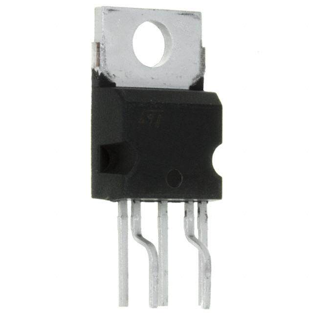
| 产品图片 |
|
| rohs | 符合RoHS无铅 / 符合限制有害物质指令(RoHS)规范要求 |
| 产品系列 | 电源管理 IC,交流/直流转换器,Power Integrations LNK302PNLinkSwitch®-TN |
| 数据手册 | |
| 产品型号 | LNK302PN |
| 产品目录页面 | |
| 产品种类 | 交流/直流转换器 |
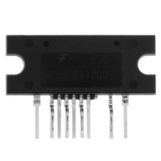
| 供应商器件封装 | DIP-8B |
| 其它名称 | 596-1021-5 |
| 功率(W) | 12mW |
| 包装 | 管件 |
| 占空比-最大 | 72 % |
| 参考设计库 | http://www.digikey.com/rdl/4294959899/4294959898/1430 |
| 商标 | Power Integrations |
| 安装风格 | Through Hole |
| 封装 | Tube |
| 封装/外壳 | 8-DIP(0.300",7.62mm),7 引线 |
| 封装/箱体 | DIP-8 |
| 工作温度 | -40°C ~ 150°C |
| 工作温度范围 | - 40 C to + 150 C |
| 工厂包装数量 | 50 |
| 开关频率 | 66 kHz |
| 标准包装 | 50 |
| 电压-击穿 | 700V |
| 电压-输入 | - |
| 电压-输出 | - |
| 电源电流 | 200 uA |
| 类型 | Off Line Switcher |
| 系列 | LNK302 |
| 输入/电源电压—最大值 | 265 VAC |
| 输入/电源电压—最小值 | 85 VAC |
| 输出电压 | 12 V |
| 输出电流 | 80 mA |
| 输出端数量 | 1 Output |
| 输出隔离 | 非隔离 |
| 频率范围 | 62kHz ~ 70kHz |


- 商务部:美国ITC正式对集成电路等产品启动337调查
- 曝三星4nm工艺存在良率问题 高通将骁龙8 Gen1或转产台积电
- 太阳诱电将投资9.5亿元在常州建新厂生产MLCC 预计2023年完工
- 英特尔发布欧洲新工厂建设计划 深化IDM 2.0 战略
- 台积电先进制程称霸业界 有大客户加持明年业绩稳了
- 达到5530亿美元!SIA预计今年全球半导体销售额将创下新高
- 英特尔拟将自动驾驶子公司Mobileye上市 估值或超500亿美元
- 三星加码芯片和SET,合并消费电子和移动部门,撤换高东真等 CEO
- 三星电子宣布重大人事变动 还合并消费电子和移动部门
- 海关总署:前11个月进口集成电路产品价值2.52万亿元 增长14.8%


PDF Datasheet 数据手册内容提取
LNK302/304-306 LinkSwitch™-TN Family Lowest Component Count, Energy-Efficient Off-Line Switcher IC Product Highlights Cost Effective Linear/Cap Dropper Replacement • Lowest cost and component count buck converter solution FB BP • Fully integrated auto-restart for short-circuit and open loop + D S + fault protection – saves external component costs Wide Range LinkSwitch-TN DC • LNK302 uses a simplified controller without auto-restart for HiDghC- VInopltuatge Output very low system cost • 66 kHz operation with accurate current limit – allows low cost PI-3492-041509 off-the-shelf 1 mH inductor for up to 120 mA output current Figure 1. Typical Buck Converter Application (See Application Examples Section • Tight tolerances and negligible temperature variation for Other Circuit Configurations). • High breakdown voltage of 700 V provides excellent input surge withstand • Frequency jittering dramatically reduces EMI (~10 dB) • Minimizes EMI filter cost • High thermal shutdown temperature (+135 °C minimum) Much Higher Performance Over Discrete Buck and Output Current Table1 Passive Solutions • Supports buck, buck-boost and flyback topologies 230 VAC ±15% 85-265 VAC Product4 • System level thermal overload, output short-circuit and open MDCM2 CCM3 MDCM2 CCM3 control loop protection LNK302P/G/D 63 mA 80 mA 63 mA 80 mA • Excellent line and load regulation even with typical configuration LNK304P/G/D 120 mA 170 mA 120 mA 170 mA • High bandwidth provides fast turn-on with no overshoot • Current limit operation rejects line ripple LNK305P/G/D 175 mA 280 mA 175 mA 280 mA • Universal input voltage range (85 VAC to 265 VAC) LNK306P/G/D 225 mA 360 mA 225 mA 360 mA • Built-in current limit and hysteretic thermal protection Table 1. Output Current Table. • Higher efficiency than passive solutions Notes: • Higher power factor than capacitor-fed solutions 1. Typical output current in a non-isolated buck converter. Output power capability • Entirely manufacturable in SMD depends on respective output voltage. See Key Applications Considerations Section for complete description of assumptions, including fully discontinuous conduction mode (DCM) operation. EcoSmart™– Extremely Energy Efficient 2. Mostly discontinuous conduction mode. • Consumes typically only 50/80 mW in self-powered buck 3. Continuous conduction mode. topology at 115/230 VAC input with no-load (opto feedback) 4. Packages: P: DIP-8B, G: SMD-8B, D: SO-8C. • Consumes typically only 7/12 mW in flyback topology with external bias at 115/230 VAC input with no-load • Meets California Energy Commission (CEC), Energy Star, and EU requirements Applications • Appliances and timers and thermal shutdown circuitry onto a monolithic IC. The start-up • LED drivers and industrial controls and operating power are derived directly from the voltage on the Description DRAIN pin, eliminating the need for a bias supply and associated circuitry in buck or flyback converters. The fully integrated LinkSwitch-TN is specifically designed to replace all linear and auto-restart circuit in the LNK304-306 safely limits output power capacitor-fed (cap dropper) non-isolated power supplies in the during fault conditions such as short-circuit or open loop, under 360 mA output current range at equal system cost while reducing component count and system-level load protection offering much higher performance and energy efficiency. cost. A local supply provided by the IC allows use of a non- LinkSwitch-TN devices integrate a 700 V power MOSFET, safety graded optocoupler acting as a level shifter to further oscillator, simple On/Off control scheme, a high-voltage switched enhance line and load regulation performance in buck and current source, frequency jittering, cycle-by-cycle current limit buck-boost converters, if required. www.powerint.com June 2013 This Product is Covered by Patents and/or Pending Patent Applications.
LNK302/304-306 BYPASS DRAIN (BP) (D) REGULATOR 5.8 V BYPASS PIN UNDERVOLTAGE + 5.8 V - 4.85 V CURRENT LIMIT COMPARATOR + 6.3 V - VI LIMIT JITTER CLOCK DC MAX FEEDBACK THERMAL SHUTDOWN (FB) OSCILLATOR 1.65 V -V T S Q R Q LEADING EDGE BLANKING SOURCE (S) PI-3904-032213 Figure 2a. Functional Block Diagram (LNK302). BYPASS DRAIN (BP) (D) REGULATOR 5.8 V FAULT PRESENT AUTO- RESTART BYPASS PIN 6.3 V COUNTER UNDERVOLTAGE + CLOCK RESET 45.8.85 VV - CCUORMRPEANRTA TLOIMRIT + - VILIMIT JITTER CLOCK DCMAX FEEDBACK THERMAL SHUTDOWN (FB) OSCILLATOR 1.65 V -VT S Q R Q LEADING EDGE BLANKING SOURCE (S) PI-2367-032213 Figure 2b. Functional Block Diagram (LNK304-306). 2 Rev. J 06/13 www.powerint.com
LNK302/304-306 Pin Functional Description DRAIN (D) Pin: for both average and quasi-peak emissions. The frequency Power MOSFET drain connection. Provides internal operating jitter should be measured with the oscilloscope triggered at the current for both start-up and steady-state operation. falling edge of the DRAIN waveform. The waveform in Figure 4 illustrates the frequency jitter of the LinkSwitch-TN. BYPASS (BP) Pin: Connection point for a 0.1 mF external bypass capacitor for the Feedback Input Circuit internally generated 5.8 V supply. The feedback input circuit at the FEEDBACK pin consists of a low impedance source follower output set at 1.65 V. When the FEEDBACK (FB) Pin: current delivered into this pin exceeds 49 mA, a low logic level During normal operation, switching of the power MOSFET is (disable) is generated at the output of the feedback circuit. This controlled by this pin. MOSFET switching is terminated when a output is sampled at the beginning of each cycle on the rising current greater than 49 mA is delivered into this pin. edge of the clock signal. If high, the power MOSFET is turned on for that cycle (enabled), otherwise the power MOSFET SOURCE (S) Pin: remains off (disabled). Since the sampling is done only at the This pin is the power MOSFET source connection. It is also the beginning of each cycle, subsequent changes in the FEEDBACK ground reference for the BYPASS and FEEDBACK pins. pin voltage or current during the remainder of the cycle are ignored. 5.8 V Regulator and 6.3 V Shunt Voltage Clamp The 5.8 V regulator charges the bypass capacitor connected to P Package (DIP-8B) the BYPASS pin to 5.8 V by drawing a current from the voltage G Package (SMD-8B) D Package (SO-8C) on the DRAIN, whenever the MOSFET is off. The BYPASS pin is the internal supply voltage node for the LinkSwitch-TN. When the MOSFET is on, the LinkSwitch-TN runs off of the energy S 1 8 S BP 1 8 S stored in the bypass capacitor. Extremely low power consumption 2 7 of the internal circuitry allows the LinkSwitch-TN to operate S 2 7 S FB S continuously from the current drawn from the DRAIN pin. A 6 BP 3 S bypass capacitor value of 0.1 mF is sufficient for both high 4 5 D S frequency decoupling and energy storage. FB 4 5 D 3a 3b In addition, there is a 6.3 V shunt regulator clamping the BYPASS pin at 6.3 V when current is provided to the BYPASS pin through an external resistor. This facilitates powering of PI-5422-060613 LinkSwitch-TN externally through a bias winding to decrease Figure 3. Pin Configuration. the no-load consumption to about 50 mW. BYPASS Pin Undervoltage LinkSwitch-TN Functional Description The BYPASS pin undervoltage circuitry disables the power MOSFET when the BYPASS pin voltage drops below 4.85 V. LinkSwitch-TN combines a high-voltage power MOSFET switch Once the BYPASS pin voltage drops below 4.85 V, it must rise with a power supply controller in one device. Unlike conventional back to 5.8 V to enable (turn-on) the power MOSFET. PWM (pulse width modulator) controllers, LinkSwitch-TN uses a simple ON/OFF control to regulate the output voltage. The Over-Temperature Protection LinkSwitch-TN controller consists of an oscillator, feedback The thermal shutdown circuitry senses the die temperature. (sense and logic) circuit, 5.8 V regulator, BYPASS pin The threshold is set at 142 °C typical with a 75 °C hysteresis. undervoltage circuit, over-temperature protection, frequency When the die temperature rises above this threshold (142 °C) jittering, current limit circuit, leading edge blanking and a 700 V the power MOSFET is disabled and remains disabled until the power MOSFET. The LinkSwitch-TN incorporates additional die temperature falls by 75 °C, at which point it is re-enabled. circuitry for auto-restart. Current Limit Oscillator The current limit circuit senses the current in the power MOSFET. The typical oscillator frequency is internally set to an average of When this current exceeds the internal threshold (I ), the 66 kHz. Two signals are generated from the oscillator: the LIMIT power MOSFET is turned off for the remainder of that cycle. maximum duty cycle signal (DC ) and the clock signal that MAX The leading edge blanking circuit inhibits the current limit indicates the beginning of each cycle. comparator for a short time (t ) after the power MOSFET is LEB turned on. This leading edge blanking time has been set so The LinkSwitch-TN oscillator incorporates circuitry that that current spikes caused by capacitance and rectifier reverse introduces a small amount of frequency jitter, typically 4 kHz recovery time will not cause premature termination of the peak-to-peak, to minimize EMI emission. The modulation rate switching pulse. of the frequency jitter is set to 1 kHz to optimize EMI reduction 3 www.powerint.com Rev. J 06/13
LNK302/304-306 600 3 flame proof, fusible, wire wound resistor. It accomplishes 0 13 several functions: a) Inrush current limitation to safe levels for 8 500 0-0 rectifiers D3 and D4; b) Differential mode noise attenuation; c) 6 400 VDRAIN PI-36 I(cnopmutp fousnee nsth foauilsld s aanfeyl yo tohpeer nc-ocmircpuoitn wenitth foauil ts ehmorittt-icnigrc sumit oke, fire or incandescent material). 300 The power processing stage is formed by the LinkSwitch-TN, 200 freewheeling diode D1, output choke L1, and the output capacitor C2. The LNK304 was selected such that the power supply 100 operates in the mostly discontinuous-mode (MDCM). Diode D1 is an ultrafast diode with a reverse recovery time (t ) of 0 RR approximately 75 ns, acceptable for MDCM operation. For 68 kHz continuous conduction mode (CCM) designs, a diode with a t 64 kHz rr of ≤35 ns is recommended. Inductor L1 is a standard off-the- shelf inductor with appropriate RMS current rating (and acceptable temperature rise). Capacitor C2 is the output filter capacitor; its 0 20 primary function is to limit the output voltage ripple. The output Time (µs) voltage ripple is a stronger function of the ESR of the output Figure 4. Frequency Jitter. capacitor than the value of the capacitor itself. Auto-Restart (LNK304-306 Only) To a first order, the forward voltage drops of D1 and D2 are In the event of a fault condition such as output overload, output identical. Therefore, the voltage across C3 tracks the output short, or an open-loop condition, LinkSwitch-TN enters into voltage. The voltage developed across C3 is sensed and auto-restart operation. An internal counter clocked by the regulated via the resistor divider R1 and R3 connected to U1’s oscillator gets reset every time the FEEDBACK pin is pulled FEEDBACK pin. The values of R1 and R3 are selected such high. If the FEEDBACK pin is not pulled high for 50 ms, the that, at the desired output voltage, the voltage at the power MOSFET switching is disabled for 800 ms. The auto- FEEDBACK pin is 1.65 V. restart alternately enables and disables the switching of the power MOSFET until the fault condition is removed. Regulation is maintained by skipping switching cycles. As the output voltage rises, the current into the FEEDBACK pin will Applications Example rise. If this exceeds I then subsequent cycles will be skipped FB until the current reduces below I . Thus, as the output load is A 1.44 W Universal Input Buck Converter FB reduced, more cycles will be skipped and if the load increases, The circuit shown in Figure 5 is a typical implementation of a fewer cycles are skipped. To provide overload protection if no 12 V, 120 mA non-isolated power supply used in appliance cycles are skipped during a 50 ms period, LinkSwitch-TN will control such as rice cookers, dishwashers or other white goods. enter auto-restart (LNK304-306), limiting the average output This circuit may also be applicable to other applications such as power to approximately 6% of the maximum overload power. night-lights, LED drivers, electricity meters, and residential Due to tracking errors between the output voltage and the heating controllers, where a non-isolated supply is acceptable. voltage across C3 at light load or no-load, a small pre-load may be required (R4). For the design in Figure 5, if regulation to zero The input stage comprises fusible resistor RF1, diodes D3 and load is required, then this value should be reduced to 2.4 kΩ. D4, capacitors C4 and C5, and inductor L2. Resistor RF1 is a R1 13.0 kΩ 1% R3 C3 8R2.2 FW 1Ω 1 Lm2H FB BP C1 2.015% kΩ 1305 µVF 1N40D025GP 100 nF 12 V, D S L1 120 mA D3 1 mH 8V5-A2C65 1N4007 4.C7 4µF 4.C7 5µF LinkLSNwKi3tc0h4-TN D1 280 mA 10C02 µF 3.R3 4kΩ D4 400 V 400 V UF4005 16 V 1N4007 RTN PI-3757-041509 Figure 5. Universal Input, 12 V, 120 mA Constant Voltage Power Supply Using LinkSwitch-TN. 4 Rev. J 06/13 www.powerint.com
LNK302/304-306 LinkSwitch-TN RF1 D3 L2 D FB D2 R1 BP + C1 AC C4 C5 S S R3 C3 L1 INPUT DC OUTPUT S S C2 D4 D1 Optimize hatched copper areas ( ) for heatsinking and EMI. PI-3750-041509 Figure 6a. Recommended Printed Circuit Layout for LinkSwitch-TN in a Buck Converter Configuration using P or G Package. RF1 D3 L2 D L S in k S S w L1 FB itch S + BP -TN S D1 INAPCU T C4 C5 C3 D2 C2 DC C1 R3 R1 OUTPUT D4 Optimize hatched copper areas ( ) for heatsinking and EMI. PI-4546-041509 Figure 6b. Recommended Printed Circuit Layout for LinkSwitch-TN in a Buck Converter Configuration using D Package to Bottom Side of the Board. Key Application Considerations LinkSwitch-TN Selection and Selection Between LinkSwitch-TN Design Considerations MDCM and CCM Operation Output Current Table Select the LinkSwitch-TN device, freewheeling diode and Data sheet maximum output current table (Table 1) represents output inductor that gives the lowest overall cost. In general, the maximum practical continuous output current for both MDCM provides the lowest cost and highest efficiency converter. mostly discontinuous conduction mode (MDCM) and continuous CCM designs require a larger inductor and ultrafast (t ≤35 ns) RR conduction mode (CCM) of operation that can be delivered freewheeling diode in all cases. It is lower cost to use a larger from a given LinkSwitch-TN device under the following LinkSwitch-TN in MDCM than a smaller LinkSwitch-TN in CCM assumed conditions: because of the additional external component costs of a CCM 1. Buck converter topology. design. However, if the highest output current is required, CCM 2. The minimum DC input voltage is ≥70 V. The value of input should be employed following the guidelines below. capacitance should be large enough to meet this criterion. 3. For CCM operation a KRP* of 0.4. Topology Options 4. Output voltage of 12 VDC. LinkSwitch-TN can be used in all common topologies, with or 5. Efficiency of 75%. without an optocoupler and reference to improve output voltage 6. A catch/freewheeling diode with t ≤75 ns is used for MDCM tolerance and regulation. Table 2 provide a summary of these RR operation and for CCM operation, a diode with t ≤35 ns is configurations. For more information see the Application Note RR used. – LinkSwitch-TN Design Guide. 7. The part is board mounted with SOURCE pins soldered to a sufficient area of copper to keep the SOURCE pin tempera- ture at or below 100 °C. *KRP is the ratio of ripple to peak inductor current. 5 www.powerint.com Rev. J 06/13
LNK302/304-306 Topology Basic Circuit Schematic Key Features High-Side 1. Output referenced to input Buck – 2. Positive output (V ) with respect to -V O IN Direct 3. Step down – V < V O IN Feedback 4. Low cost direct feedback (±10% typ.) FB BP 5. Requires an output load to maintain regulation + D S + V LinkSwitch-TN V IN O PI-3751-041509 High-Side 1. Output referenced to input Buck – 2. Positive output (V ) with respect to -V O IN Optocoupler FB BP 3. Step down – V < V O IN Feedback 4. Optocoupler feedback + D S + - Accuracy only limited by reference choice LinkSwitch-TN - Low cost non-safety rated optocoupler V V IN O - No pre-load required 5. Minimum no-load consumption PI-3752-041509 Low-Side Buck – + + Optocoupler Feedback LinkSwitch-TN V V IN O BP FB 1. Output referenced to input S D 2. Negative output (V ) with respect to +V PI-3753-041509 O IN 3. Step down – V < V Low-Side O IN + 4. Optocoupler feedback Buck – I O - Accuracy only limited by reference choice Constant - Low cost non-safety rated optocoupler Current LED LinkSwitch-TN Driver VIN VF+ - No pre-load required - Ideal for driving LEDs BP FB S D V PI-3754-041509 R = F I O High-Side Buck-Boost – Direct Feedback FB BP + D S LinkSwitch-TN 1. Output referenced to input V V IN O 2. Negative output (V ) with respect to +V + O IN 3. Step up/down – V > V orV < V O IN O IN PI-3755-041509 4. Low cost direct feedback (±10% typ.) High-Side 5. Fail-safe – output is not subjected to input 2 V Buck-Boost – 300 Ω R = voltage if the internal power MOSFET fails SENSE I Constant 2 kΩ O 6. Ideal for driving LEDs – better accuracy and Current LED FB BP RSENSE IO temperature stability than Low-side Buck Driver + D S constant current LED driver LinkSwitch-TN VIN 10 µF 100 nF 7. Requires an output load to maintain regulation 50 V PI-3779-041509 Table 2. Common Circuit Configurations Using LinkSwitch-TN. (continued on next page) 6 Rev. J 06/13 www.powerint.com
LNK302/304-306 Topology Basic Circuit Schematic Key Features Low-Side 1. Output referenced to input Buck-Boost – + 2. Positive output (V ) with respect to +V O IN Optocoupler 3. Step up/down – V > V or V < V O IN O IN Feedback 4. Optocoupler feedback LinkSwitch-TN V V - Accuracy only limited by reference choice IN O - Low cost non-safety rated optocoupler - No pre-load required BP FB + 5. Fail-safe – output is not subjected to input S D voltage if the internal power MOSFET fails PI-3756-041509 6. Minimum no-load consumption Table 2 (cont). Common Circuit Configurations Using LinkSwitch-TN. Component Selection should not exceed the rated ripple voltage divided by the typical current limit of the chosen LinkSwitch-TN. Referring to Figure 5, the following considerations may be helpful in selecting components for a LinkSwitch-TN design. Feedback Resistors R1 and R3 The values of the resistors in the resistor divider formed by R1 Freewheeling Diode D1 and R3 are selected to maintain 1.65 V at the FEEDBACK pin. It Diode D1 should be an ultrafast type. For MDCM, reverse is recommended that R3 be chosen as a standard 1% resistor recovery time t ≤75 ns should be used at a temperature of of 2 kΩ. This ensures good noise immunity by biasing the RR 70 °C or below. Slower diodes are not acceptable, as continuous feedback network with a current of approximately 0.8 mA. mode operation will always occur during startup, causing high leading edge current spikes, terminating the switching cycle Feedback Capacitor C3 prematurely, and preventing the output from reaching regulation. Capacitor C3 can be a low cost general purpose capacitor. It If the ambient temperature is above 70 °C then a diode with t provides a “sample and hold” function, charging to the output RR ≤35 ns should be used. voltage during the off time of LinkSwitch-TN. Its value should be 10 mF to 22 mF; smaller values cause poorer regulation at For CCM an ultrafast diode with reverse recovery time t ≤35 ns light load conditions. RR should be used. A slower diode may cause excessive leading edge current spikes, terminating the switching cycle prematurely Pre-Load Resistor R4 In high-side, direct feedback designs where the minimum load and preventing full power delivery. is <3 mA, a pre-load resistor is required to maintain output regulation. This ensures sufficient inductor energy to pull the Fast and slow diodes should never be used as the large reverse inductor side of the feedback capacitor C3 to input return via recovery currents can cause excessive power dissipation in the D2. The value of R4 should be selected to give a minimum diode and/or exceed the maximum drain current specification output load of 3 mA. of LinkSwitch-TN. Feedback Diode D2 In designs with an optocoupler the Zener or reference bias Diode D2 can be a low-cost slow diode such as the 1N400X current provides a 1 mA to 2 mA minimum load, preventing series, however it should be specified as a glass passivated “pulse bunching” and increased output ripple at zero load. type to guarantee a specified reverse recovery time. To a first LinkSwitch-TN Layout Considerations order, the forward drops of D1 and D2 should match. In the buck or buck-boost converter configuration, since the Inductor L1 SOURCE pins in LinkSwitch-TN are switching nodes, the Choose any standard off-the-shelf inductor that meets the copper area connected to SOURCE should be minimized to design requirements. A “drum” or “dog bone” “I” core inductor minimize EMI within the thermal constraints of the design. is recommended with a single ferrite element due to its low cost and very low audible noise properties. The typical inductance In the boost configuration, since the SOURCE pins are tied to value and RMS current rating can be obtained from the DC return, the copper area connected to SOURCE can be LinkSwitch-TN design spreadsheet available within the PI Expert maximized to improve heat sinking. design suite from Power Integrations. Choose L1 greater than or equal to the typical calculated inductance with RMS current The loop formed between the LinkSwitch-TN, inductor (L1), rating greater than or equal to calculated RMS inductor current. freewheeling diode (D1), and output capacitor (C2) should be Capacitor C2 kept as small as possible. The BYPASS pin capacitor C1 The primary function of capacitor C2 is to smooth the inductor (Figure 6) should be located physically close to the SOURCE (S) current. The actual output ripple voltage is a function of this and BYPASS (BP) pins. To minimize direct coupling from capacitor’s ESR. To a first order, the ESR of this capacitor switching nodes, the LinkSwitch-TN should be placed away 7 www.powerint.com Rev. J 06/13
LNK302/304-306 from AC input lines. It may be advantageous to place capacitors 3. Maximum drain current – verify that the peak drain current is C4 and C5 in-between LinkSwitch-TN and the AC input. The below the data sheet peak drain specification under worst- second rectifier diode D4 is optional, but may be included for case conditions of highest line voltage, maximum overload better EMI performance and higher line surge withstand (just prior to auto-restart) and highest ambient temperature. capability. 4. Thermal check – at maximum output power, minimum input voltage and maximum ambient temperature, verify that the Quick Design Checklist LinkSwitch-TN SOURCE pin temperature is 100 °C or below. This figure ensures adequate margin due to variations in As with any power supply design, all LinkSwitch-TN designs R from part to part. A battery powered thermocouple should be verified for proper functionality on the bench. The DS(ON) meter is recommended to make measurements when the following minimum tests are recommended: SOURCE pins are a switching node. Alternatively, the 1. Adequate DC rail voltage – check that the minimum DC input ambient temperature may be raised to indicate margin to voltage does not fall below 70 VDC at maximum load, thermal shutdown. minimum input voltage. 2. Correct Diode Selection – UF400x series diodes are recom- In a LinkSwitch-TN design using a buck or buck-boost converter mended only for designs that operate in MDCM at an topology, the SOURCE pin is a switching node. Oscilloscope ambient of 70 °C or below. For designs operating in measurements should therefore be made with probe grounded continuous conduction mode (CCM) and/or higher ambients, to a DC voltage, such as primary return or DC input rail, and not then a diode with a reverse recovery time of 35 ns or better, to the SOURCE pins. The power supply input must always be such as the BYV26C, is recommended. supplied from an isolated source (e.g. via an isolation transformer). 8 Rev. J 06/13 www.powerint.com
LNK302/304-306 Absolute Maximum Ratings(1,5) DRAIN Pin Voltage ..............................................-0.3 V to 700 V Notes: DRAIN Pin Peak Current: LNK302 ......................200 (375) mA(2) 1. All voltages referenced to SOURCE, T = 25 °C. A LNK304 ......................400 (750) mA(2) 2. The higher peak DRAIN current is allowed if the DRAIN LNK305 ....................800 (1500) mA(2) to SOURCE voltage does not exceed 400 V. LNK306 ..................1400 (2600) mA(2) 3. Normally limited by internal circuitry. FEEDBACK Pin Voltage ..........................................-0.3 V to 9 V 4. 1/16 in. from case for 5 seconds. FEEDBACK Pin Current .................................................100 mA 5. Maximum ratings specified may be applied, one at a time, BYPASS Pin Voltage ...............................................-0.3 V to 9 V without causing permanent damage to the product. Storage Temperature .....................................-65 °C to 150 °C Exposure to Absolute Maximum Rating conditions for Operating Junction Temperature(3) ..................-40 °C to 150 °C extended periods of time may affect product reliability. Lead Temperature(4) .........................................................260 °C Thermal Resistance Thermal Resistance: P or G Package: Notes: (q ) ................................70 °C/W(3); 60 °C/W(4) 1. Measured on pin 2 (SOURCE) close to plastic interface. JA (q )(1) .................................................11 °C/W 2. Measured on pin 8 (SOURCE) close to plastic interface. JC D Package: 3. Soldered to 0.36 sq. in. (232 mm2), 2 oz. (610 g/m2) copper clad. (q ) ..................... .........100 °C/W(3); 80 °C/W(4) 4. Soldered to 1 sq. in. (645 mm2), 2 oz. (610 g/m2) copper clad. JA (q )(2) .................................................30 °C/W JC Conditions SOURCE = 0 V; T = -40 to 125 °C Parameter Symbol See FigJure 7 Min Typ Max Units (Unless Otherwise Specified) Control Functions Average 62 66 70 Output f T = 25 °C kHz Frequency OSC J Peak-Peak Jitter 4 Maximum Duty Cycle DC S2 Open 66 69 72 % MAX FEEDBACK Pin Turnoff I T = 25 °C 30 49 68 mA Threshold Current FB J FEEDBACK Pin Voltage V 1.54 1.65 1.76 V at Turnoff Threshold FB V ≥2 V FB I (MOSFET Not Switching) 160 220 mA S1 See Note A DRAIN Pin FEEDBACK Open LNK302/304 200 260 Supply Current (MOSFET I LNK305 220 280 mA S2 Switching) See Notes A, B LNK306 250 310 LNK302/304 -5.5 -3.3 -1.8 V = 0 V I BP CH1 T = 25 °C BYPASS Pin J LNK305/306 -7.5 -4.6 -2.5 mA Charge Current LNK302/304 -3.8 -2.3 -1.0 V = 4 V I BP CH2 T = 25 °C J LNK305/306 -4.5 -3.3 -1.5 9 www.powerint.com Rev. J 06/13
LNK302/304-306 Conditions SOURCE = 0 V; T = -40 to 125 °C Parameter Symbol J Min Typ Max Units See Figure 7 (Unless Otherwise Specified) Control Functions (cont.) BYPASS Pin V 5.55 5.8 6.10 V Voltage BP BYPASS Pin V 0.8 0.95 1.2 V Voltage Hysteresis BPH BYPASS Pin I See Note D 68 mA Supply Current BPSC Circuit Protection di/dt = 55 mA/s 126 136 146 T = 25 °C J LNK302 di/dt = 250 mA/s 145 165 185 T = 25 °C J di/dt = 65 mA/s 240 257 275 T = 25 °C J LNK304 di/dt = 415 mA/s 271 308 345 I (See T = 25 °C Current Limit LIMIT J mA Note E) di/dt = 75 mA/s 350 375 401 T = 25 °C J LNK305 di/dt = 500 mA/s 396 450 504 T = 25 °C J di/dt = 95 mA/s 450 482 515 T = 25 °C J LNK306 di/dt = 610 mA/s 508 578 647 T = 25 °C J LNK302/304 280 360 475 Minimum On Time t LNK305 360 460 610 ns ON(MIN) LNK306 400 500 675 Leading Edge T = 25 °C t J 170 215 ns Blanking Time LEB See Note F Thermal Shutdown T 135 142 150 °C Temperature SD Thermal Shutdown T See Note G 75 °C Hysteresis SHD 10 Rev. J 06/13 www.powerint.com
LNK302/304-306 Conditions SOURCE = 0 V; T = -40 to 125 °C Parameter Symbol J Min Typ Max Units See Figure 7 (Unless Otherwise Specified) Output T = 25 °C 48 55.2 LNK302 J ID = 13 mA TJ = 100 °C 76 88.4 T = 25 °C 24 27.6 LNK304 J ON-State ID = 25 mA TJ = 100 °C 38 44.2 R Ω Resistance DS(ON) T = 25 °C 12 13.8 LNK305 J ID = 35 mA TJ = 100 °C 19 22.1 T = 25 °C 7 8.1 LNK306 J ID = 45 mA TJ = 100 °C 11 12.9 LNK302/304 50 V = 6.2 V, V ≥2 V, OFF-State Drain BP FB I V = 560 V, LNK305 70 mA Leakage Current DSS DS T = 25 °C J LNK306 90 V = 6.2 V, V ≥2 V, Breakdown Voltage BV BP FB 700 V DSS T = 25 °C J Rise Time t 50 ns R Measured in a Typical Buck Fall Time t Converter Application 50 ns F DRAIN Pin 50 V Supply Voltage Output Enable Delay t See Figure 9 10 ms EN Output Disable t 0.5 ms Setup Time DST Auto-Restart T = 25 °C LNK302 Not Applicable t J ms ON-Time AR See Note H LNK304-306 50 Auto-Restart LNK302 Not Applicable DC % Duty Cycle AR LNK304-306 6 Notes: A. Total current consumption is the sum of I and I when FEEDBACK pin voltage is ≥2 V (MOSFET not switching) and the sum of S1 DSS I and I when FEEDBACK pin is shorted to SOURCE (MOSFET switching). S2 DSS B. Since the output MOSFET is switching, it is difficult to isolate the switching current from the supply current at the DRAIN. An alternative is to measure the BYPASS pin current at 6 V. C. See Typical Performance Characteristics section Figure 14 for BYPASS pin start-up charging waveform. D. This current is only intended to supply an optional optocoupler connected between the BYPASS and FEEDBACK pins and not any other external circuitry. E. For current limit at other di/dt values, refer to Figure 13. F. This parameter is guaranteed by design. G. This parameter is derived from characterization. H. Auto-restart on time has the same temperature characteristics as the oscillator (inversely proportional to frequency). 11 www.powerint.com Rev. J 06/13
LNK302/304-306 470 Ω 5 W 470 kΩ D FB S1 S2 BP 50 V 50 V S S 0.1 μF S S PI-3490-060204 Figure 7. LinkSwitch-TN General Test Circuit. DC MAX (internal signal) tP FB V tEN DRAIN 1 t = P f OSC PI-3707-112503 Figure 8. LinkSwitch-TN Duty Cycle Measurement. Figure 9. LinkSwitch-TN Output Enable Timing. 12 Rev. J 06/13 www.powerint.com
LNK302/304-306 Typical Performance Characteristics wn Voltageed to 25 C)°11..10 PI-2213-012301 Frequencyed to 25 C)°1100....2086 PI-2680-012301 akdomaliz tput maliz0.4 BreNor OuNor ( (0.2 0.9 0 -50 -25 0 25 50 75 100 125 150 -50 -25 0 25 50 75 100 125 Junction Temperature (°C) Junction Temperature (°C) Figure 10. Breakdown vs. Temperature. Figure 11. Frequency vs. Temperature. C) 11..24 PI-3709-111203 Limit 11..24 PI-3710-071204 t5 °1.0 nt 1.0 t Limid to 2 0.8 Curre 0.8 Normalized Currenormalize 00..64 Normalizddeiid//dd dtt i==/d 16t malized 00..64 LLNNKK330024 Nd56i55o/d rmmmt =AAa //l1µµizssed CL12i35um67rri temm =nAA t1 N r LNK305 75 mA/µs 375 mA ( 0.2 No 0.2 LNK306 95 mA/µs 482 mA 0 0 -50 0 50 100 150 1 2 3 4 5 6 Temperature (°C) Normalized di/dt Figure 12. Current Limit vs. Temperature at Normalized di/dt. Figure 13. Current Limit vs. di/dt. ge (V) 765 PI-2240-012301 t (mA) 334050000 25 °C 100 °C PI-3661-060613 a n olt 4 rre 250 V u n 3 C 200 Pi n S 2 Pi 150 S N Scaling Factors: YPA 1 RAI 100 LLNNKK330024 01..50 B D LNK305 2.0 0 50 LNK306 3.4 0 0 0.2 0.4 0.6 0.8 1.0 0 2 4 6 8 10 12 14 16 18 20 Time (ms) DRAIN Voltage (V) Figure 14. BYPASS Pin Start-up Waveform. Figure 15. Output Characteristics. 13 www.powerint.com Rev. J 06/13
LNK302/304-306 Typical Performance Characteristics (cont.) F) 1000 PI-3711-071404 p ( e 100 c n Scaling Factors: ta LNK302 0.5 ci LNK304 1.0 a p LNK305 2.0 a LNK306 3.4 C n 10 ai r D 1 0 100 200 300 400 500 600 Drain Voltage (V) Figure 16. C vs. Drain Voltage. OSS Part Ordering Information • LinkSwitch Product Family • TN Series Number • Package Identifier G Plastic Surface Mount DIP P Plastic DIP D Plastic SO-8C • Package Material N Pure Matte Tin (RoHS Compliant) G RoHS Compliant and Halogen Free (D package only) • Tape & Reel and Other Options Blank Standard Configurations LNK 304 G N - TL TL Tape and Reel, 1 k pcs minimum for G Package. 2.5 k pcs for D Package. Not available for P Package. 14 Rev. J 06/13 www.powerint.com
LNK302/304-306 PDIP-8B (P Package) ⊕D S .004 (.10) .137 (3.48) Notes: -E- MINIMUM 1. Package dimensions conform to JEDEC specification MS-001-AB (Issue B 7/85) for standard dual-in-line (DIP) package with .300 inch row spacing. 2. Controlling dimensions are inches. Millimeter sizes are shown in parentheses. 3. Dimensions shown do not include mold flash or other .240 (6.10) protrusions. Mold flash or protrusions shall not exceed .260 (6.60) .006 (.15) on any side. 4. Pin locations start with Pin 1, and continue counter-clock- wise to Pin 8 when viewed from the top. The notch and/or dimple are aids in locating Pin 1. Pin 6 is omitted. 5. Minimum metal to metal spacing at the package body for the omitted lead location is .137 inch (3.48 mm). Pin 1 6. Lead width measured at package body. 7. Lead spacing measured with the leads constrained to be .367 (9.32) perpendicular to plane T. -D- .387 (9.83) .057 (1.45) .068 (1.73) (NOTE 6) .125 (3.18) .015 (.38) .145 (3.68) MINIMUM -T- SEATING .008 (.20) PLANE .120 (3.05) .015 (.38) .140 (3.56) .300 (7.62) BSC .100 (2.54) BSC .048 (1.22) (NOTE 7) .053 (1.35) P08B .014 (.36) .300 (7.62) .022 (.56) ⊕T E D S .010 (.25) M .390 (9.91) PI-2551-040110 SMD-8B (G Package) ⊕D S.004 (.10) .137 (3.48) Notes: MINIMUM 1. Controlling dimensions are inches. Millimeter sizes are -E- shown in parentheses. 2. Dimensions shown do not include mold flash or other protrusions. Mold flash or protrusions shall not exceed .006 (.15) on any side. .372 (9.45) .240 (6.10) 3. Pin locations start with Pin 1, .260 (6.60) .388 (9.86) .420 and continue counter-clock- ⊕E S.010 (.25) wise to Pin 8 when viewed .046 .060 .060 .046 from the top. Pin 6 is omitted. 4. Minimum metal to metal spacing at the package body for the omitted lead location Pin 1 Pin 1 .080 is .137 inch (3.48 mm). 5. Lead width measured at .100 (2.54) (BSC) .086 package body. 6. D and E are referenced .186 datums on the package .286 body. .367 (9.32) -D- Solder Pad Dimensions .387 (9.83) .057 (1.45) .125 (3.18) .068 (1.73) .145 (3.68) (NOTE 5) .004 (.10) .032 (.81) .048 (1.22) .037 (.94) .053 (1.35) .009 (.23) .004 (.10) .036 (0.91) 0 °-8° .012 (.30) .044 (1.12) G08B PI-2546-040110 15 www.powerint.com Rev. J 06/13
LNK302/304-306 SO-8C (D Package) 0.10 (0.004) C A-B2X 2 DETAIL A 4 B 4.90 (0.193) BSC A 4 D 8 5 GAUGE PLANE SEATING PLANE 2 3.90 (0.154) BSC 6.00 (0.236) BSC C 0 - 8o 0.25 (0.010) 1.04 (0.041) REF BSC 0.10 (0.004) C D 0.40 (0.016) 2X Pin 1 ID 1 4 0.20 (0.008) C 1.27 (0.050) 1.27 (0.050) BSC 2X 7X 0.31 - 0.51 (0.012 - 0.020) 0.25 (0.010) M CA-BD 1.35 (0.053) 1.25 - 1.65 DETAIL A 1.75 (0.069) (0.049 - 0.065) 0.10 (0.004) 0.10 (0.004) C H 0.25 (0.010) 7X SEATING PLANE 0.17 (0.007) C 0.25 (0.010) Reference Solder Pad + Dimensions Notes: 1. JEDEC reference: MS-012. 2.00 (0.079) 4.90 (0.193) 2. Package outline exclusive of mold flash and metal burr. 3. Package outline inclusive of plating thickness. 4. Datums A and B to be determined at datum plane H. + + + 5. Controlling dimensions are in millimeters. Inch dimensions are shown in parenthesis. Angles in degrees. D07C 1.27 (0.050) 0.60 (0.024) PI-4526-040110 16 Rev. J 06/13 www.powerint.com
LNK302/304-306 Revision Notes Date C Release data sheet. 03/03 D Corrected Minimum On-Time. 01/04 E Added LNK302. 08/04 F Added lead-free ordering information. 12/04 Minor error corrections. G 03/05 Renamed Feedback Pin Voltage Parameter to Feedback Pin Voltage at Turnoff Threshold and removed condition. H Added SO-8C package. 12/06 I Updated Part Ordering Information section with Halogen Free. 11/08 J Updated Key Features column in Table 2. Updated style of data sheet. 06/13 17 www.powerint.com Rev. J 06/13
For the latest updates, visit our website: www.powerint.com Power Integrations reserves the right to make changes to its products at any time to improve reliability or manufacturability. Power Integrations does not assume any liability arising from the use of any device or circuit described herein. POWER INTEGRATIONS MAKES NO WARRANTY HEREIN AND SPECIFICALLY DISCLAIMS ALL WARRANTIES INCLUDING, WITHOUT LIMITATION, THE IMPLIED WARRANTIES OF MERCHANTABILITY, FITNESS FOR A PARTICULAR PURPOSE, AND NON-INFRINGEMENT OF THIRD PARTY RIGHTS. Patent Information The products and applications illustrated herein (including transformer construction and circuits external to the products) may be covered by one or more U.S. and foreign patents, or potentially by pending U.S. and foreign patent applications assigned to Power Integrations. A complete list of Power Integrations patents may be found at www.powerint.com. Power Integrations grants its customers a license under certain patent rights as set forth at http://www.powerint.com/ip.htm. Life Support Policy POWER INTEGRATIONS PRODUCTS ARE NOT AUTHORIZED FOR USE AS CRITICAL COMPONENTS IN LIFE SUPPORT DEVICES OR SYSTEMS WITHOUT THE EXPRESS WRITTEN APPROVAL OF THE PRESIDENT OF POWER INTEGRATIONS. As used herein: 1. A Life support device or system is one which, (i) is intended for surgical implant into the body, or (ii) supports or sustains life, and (iii) whose failure to perform, when properly used in accordance with instructions for use, can be reasonably expected to result in significant injury or death to the user. 2. A critical component is any component of a life support device or system whose failure to perform can be reasonably expected to cause the failure of the life support device or system, or to affect its safety or effectiveness. The PI logo, TOPSwitch, TinySwitch, LinkSwitch, LYTSwitch, DPA-Switch, PeakSwitch, CAPZero, SENZero, LinkZero, HiperPFS, HiperTFS, HiperLCS, Qspeed, EcoSmart, Clampless, E-Shield, Filterfuse, StakFET, PI Expert and PI FACTS are trademarks of Power Integrations, Inc. Other trademarks are property of their respective companies. ©2014, Power Integrations, Inc. Power Integrations Worldwide Sales Support Locations World Headquarters Germany Japan Taiwan 5245 Hellyer Avenue Lindwurmstrasse 114 Kosei Dai-3 Bldg. 5F, No. 318, Nei Hu Rd., Sec. 1 San Jose, CA 95138, USA. 80337 Munich 2-12-11, Shin-Yokohama, Nei Hu Dist. Main: +1-408-414-9200 Germany Kohoku-ku Taipei 11493, Taiwan R.O.C. Customer Service: Phone: +49-895-527-39110 Yokohama-shi Kanagwan Phone: +886-2-2659-4570 Phone: +1-408-414-9665 Fax: +49-895-527-39200 222-0033 Japan Fax: +886-2-2659-4550 Fax: +1-408-414-9765 e-mail: eurosales@powerint.com Phone: +81-45-471-1021 e-mail: taiwansales@powerint.com e-mail: usasales@powerint.com Fax: +81-45-471-3717 India e-mail: japansales@powerint.com UK China (Shanghai) #1, 14th Main Road First Floor, Unit 15, Meadway Rm 1601/1610, Tower 1, Vasanthanagar Korea Court, Rutherford Close, Kerry Everbright City Bangalore-560052 India RM 602, 6FL Stevenage, Herts. SG1 2EF No. 218 Tianmu Road West, Phone: +91-80-4113-8020 Korea City Air Terminal B/D, 159-6 United Kingdom Shanghai, P.R.C. 200070 Fax: +91-80-4113-8023 Samsung-Dong, Kangnam-Gu, Phone: +44 (0) 1252-730-141 Phone: +86-21-6354-6323 e-mail: indiasales@powerint.com Seoul, 135-728, Korea Fax: +44 (0) 1252-727-689 Fax: +86-21-6354-6325 Phone: +82-2-2016-6610 e-mail: eurosales@powerint.com e-mail: chinasales@powerint.com Italy Fax: +82-2-2016-6630 Via Milanese 20, 3rd. Fl. e-mail: koreasales@powerint.com Applications Hotline China (ShenZhen) 20099 Sesto San Giovanni (MI) World Wide +1-408-414-9660 3rd Floor, Block A, Italy Singapore Zhongtou International Business Phone: +39-024-550-8701 51 Newton Road Applications Fax Center, No. 1061, Xiang Mei Rd, Fax: +39-028-928-6009 #19-01/05 Goldhill Plaza World Wide +1-408-414-9760 FuTian District, ShenZhen, e-mail: eurosales@powerint.com Singapore, 308900 China, 518040 Phone: +65-6358-2160 Phone: +86-755-8379-3243 Fax: +65-6358-2015 Fax: +86-755-8379-5828 e-mail: singaporesales@powerint.com e-mail: chinasales@powerint.com
Mouser Electronics Authorized Distributor Click to View Pricing, Inventory, Delivery & Lifecycle Information: P ower Integrations: LNK304PN LNK304GN LNK306GN-TL LNK306PN LNK306GN LNK302GN LNK302PN LNK302GN-TL LNK305PN LNK305GN LNK305GN-TL LNK302DG LNK302DG-TL LNK304DG LNK304DG-TL LNK305DG LNK305DG-TL LNK306DG LNK306DG-TL LNK302DN LNK302DN-TL LNK304DN LNK304DN-TL LNK305DN LNK305DN-TL LNK306DN LNK306DN-TL