ICGOO在线商城 > 集成电路(IC) > PMIC - AC-DC 转换器,离线开关 > NCP1075STBT3G
 Datasheet下载
- 型号: NCP1075STBT3G
- 制造商: ON Semiconductor
- 库位|库存: xxxx|xxxx
- 要求:
| 数量阶梯 | 香港交货 | 国内含税 |
| +xxxx | $xxxx | ¥xxxx |
查看当月历史价格
查看今年历史价格
NCP1075STBT3G产品简介:
ICGOO电子元器件商城为您提供NCP1075STBT3G由ON Semiconductor设计生产,在icgoo商城现货销售,并且可以通过原厂、代理商等渠道进行代购。 NCP1075STBT3G价格参考。ON SemiconductorNCP1075STBT3G封装/规格:PMIC - AC-DC 转换器,离线开关, Converter Offline Flyback Topology 100kHz SOT-223 (TO-261)。您可以下载NCP1075STBT3G参考资料、Datasheet数据手册功能说明书,资料中有NCP1075STBT3G 详细功能的应用电路图电压和使用方法及教程。
NCP1075STBT3G 是 ON Semiconductor 生产的一款 PMIC(电源管理集成电路),专门用于 AC-DC 转换器中的离线开关应用。这款芯片具有高集成度、高效能和紧凑设计的特点,适用于多种需要将交流电转换为直流电的设备。

 应用场景

1. 消费电子产品:
   - 充电器和适配器:NCP1075STBT3G 可广泛应用于手机、平板电脑、笔记本电脑等便携式电子设备的充电器和适配器中。它能够提供稳定的直流输出,确保设备安全充电。
   - 家电产品:如电视、音响系统、微波炉等家用电器中,该芯片可以作为电源管理的核心组件,实现高效的电源转换,提升产品的性能和可靠性。

2. 工业设备:
   - 工业控制系统:在工业自动化领域,NCP1075STBT3G 可用于各种控制器、传感器和执行器的电源管理,确保这些设备在复杂的工作环境中稳定运行。
   - 通信设备:如路由器、交换机等网络设备中,该芯片可以提供稳定的电源供应,保证数据传输的可靠性和稳定性。

3. 照明系统:
   - LED 照明:在 LED 照明系统中,NCP1075STBT3G 可以用于驱动电路,将市电转换为适合 LED 工作的直流电压,提高照明效率并延长灯具寿命。
   - 智能照明:在智能家居或商业照明系统中,该芯片可以集成到智能控制模块中,实现对灯光亮度、颜色等参数的精确控制。

4. 医疗设备:
   - 便携式医疗设备:如血压计、血糖仪等小型医疗设备中,NCP1075STBT3G 可以提供稳定的电源,确保测量结果的准确性。
   - 大型医疗设备:如 X 光机、超声波设备等,该芯片可以用于电源管理系统,确保设备在长时间工作中的稳定性和安全性。

总之,NCP1075STBT3G 凭借其高效、紧凑和可靠的特性,在多个领域的电源管理应用中表现出色,能够满足不同应用场景下的需求。
| 参数 | 数值 |
| 产品目录 | 集成电路 (IC)半导体 |
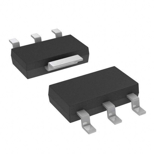
| 描述 | IC REG SW OFFLINE SMPS SOT-223-4交流/直流转换器 |
| 产品分类 | |
| 品牌 | ON Semiconductor |
| 产品手册 | |
| 产品图片 |
|
| rohs | 符合RoHS无铅 / 符合限制有害物质指令(RoHS)规范要求 |
| 产品系列 | 电源管理 IC,交流/直流转换器,ON Semiconductor NCP1075STBT3G- |
| 数据手册 | |
| 产品型号 | NCP1075STBT3G |
| 产品种类 | 交流/直流转换器 |
| 供应商器件封装 | SOT-223 |
| 其它名称 | NCP1075STBT3GOSDKR |
| 功率(W) | 19W |
| 包装 | Digi-Reel® |
| 占空比-最大 | 72 % |
| 商标 | ON Semiconductor |
| 安装风格 | SMD/SMT |
| 封装 | Reel |
| 封装/外壳 | TO-261-4,TO-261AA |
| 封装/箱体 | SOT-223 |
| 工作温度 | -40°C ~ 125°C |
| 工作电源电流 | 0.7 mA |
| 工厂包装数量 | 4000 |
| 开关频率 | 100 kHz |
| 拓扑结构 | Flyback |
| 标准包装 | 1 |
| 特色产品 | http://www.digikey.cn/product-highlights/cn/zh/on-semiconductor-ncp107-switching-regulators/3436 |
| 电压-击穿 | 700V |
| 电压-输入 | 6.3 V ~ 10 V |
| 电压-输出 | - |
| 类型 | Current Mode PWM Controllers |
| 系列 | NCP1075 |
| 绝缘 | Isolated |
| 输入电压 | 8.2 V |
| 输出电流 | 450 mA |
| 输出端数量 | 1 Output |
| 输出隔离 | 隔离 |
| 频率范围 | 90kHz ~ 110kHz |


- 商务部:美国ITC正式对集成电路等产品启动337调查
- 曝三星4nm工艺存在良率问题 高通将骁龙8 Gen1或转产台积电
- 太阳诱电将投资9.5亿元在常州建新厂生产MLCC 预计2023年完工
- 英特尔发布欧洲新工厂建设计划 深化IDM 2.0 战略
- 台积电先进制程称霸业界 有大客户加持明年业绩稳了
- 达到5530亿美元!SIA预计今年全球半导体销售额将创下新高
- 英特尔拟将自动驾驶子公司Mobileye上市 估值或超500亿美元
- 三星加码芯片和SET,合并消费电子和移动部门,撤换高东真等 CEO
- 三星电子宣布重大人事变动 还合并消费电子和移动部门
- 海关总署:前11个月进口集成电路产品价值2.52万亿元 增长14.8%


PDF Datasheet 数据手册内容提取
NCP1070, NCP1071, NCP1072, NCP1075, NCP1076, NCP1077 High-Voltage Switcher for Low Power Offline SMPS www.onsemi.com The NCP107x products integrate a fixed frequency current mode controller with a 700 V MOSFET. Available in a PDIP−7 or SOT−223 package, the NCP107x offer a high level of integration, including MARKING soft−start, frequency−jittering, short−circuit protection, skip−cycle, a DIAGRAMS maximum peak current set point, ramp compensation, and a Dynamic Self−Supply (eliminating the need for an auxiliary winding). SOT−223 AYW Unlike other monolithic solutions, the NCP107x is quiet by nature: ST SUFFIX z07xy(cid:2) during nominal load operation, the part switches at one of the available CASE 318E (cid:2) frequencies (65, 100 or 130 kHz). When the output power demand 1 diminishes, the IC automatically enters frequency foldback mode and provides excellent efficiency at light loads. When the power demand reduces further, it enters into a skip mode to reduce the standby PDIP−7 P107xfyyy consumption down to a no load condition. P SUFFIX AWL Protection features include: a timer to detect an overload or a CASE 626A YYWWG short−circuit event, Overvoltage Protection with auto−recovery and AC input line voltage detection. Z = 1 for Std product; V for Automotive For improved standby performance, the connection of an auxiliary x = Current Limit (0, 1, 2, 5, 6 or 7) winding stops the DSS operation and helps to reduce input power y = Oscillator Frequency consumption below 50 mW at high line. = A (65 kHz), B (100 kHz), C (130 kHz) yyy = 065, 100, 130 Features f = OFF phase in fault mode • Built−in 700 V MOSFET with R of 4.7 (cid:2) (NCP1076/77) / = P (420 ms), B (210 ms) DS(on) 11(cid:2) (NCP1072/75) / 22 (cid:2) (NCP1070/71) A = Assembly Location WL = Wafer Lot • Large Creepage Distance Between High−voltage Pins Y, YY = Year • Current−Mode Fixed Frequency Operation – 65 / 100 / 130 kHz W, WW = Work Week • G or (cid:2) = Pb−Free Package Peak Current: NCP1070/72 with 250 mA, NCP1071 with 350 mA, NCP1075 with 450 mA, NCP1076 with 650 mA and NCP1077 with ORDERING INFORMATION 800mA See detailed ordering and shipping information on page 28 of • Fixed Ramp Compensation this data sheet. • Skip−Cycle Operation at Low Peak Currents Only: No Acoustic Noise! • • Dynamic Self−Supply: No Need for an Auxiliary No Load Input Consumption < 50 mW Winding • Frequency Foldback to Improve Efficiency at Light • Internal 1 ms Soft−Start Load • • Auto−Recovery Output Short Circuit Protection with Internal Temperature Shutdown Timer−Based Detection • These are Pb−Free Devices • Auto−Recovery Overvoltage Protection with Auxiliary Typical Applications Winding Operation • • Auxiliary / Standby Isolated Power Supplies White Frequency Jittering for Better EMI Signature, Including Goods / Smart Meter / E−Meter Frequency Foldback Mode © Semiconductor Components Industries, LLC, 2016 1 Publication Order Number: March, 2018 − Rev. 9 NCP1070/D
NCP1070, NCP1071, NCP1072, NCP1075, NCP1076, NCP1077 PIN CONNECTIONS VCC 1 8 GND VCC 1 2 7 GND FB 2 4 GND GND 3 DRAIN 3 FB 4 5 DRAIN (Top View) (Top View) SOT−223 PDIP−7 Figure 1. Pin Connections INDICATIVE MAXIMUM OUTPUT POWER RDS(on) − IIPK 230 Vac 85−265 Vac NCP1070 / 1071 22 (cid:2) − 350 mA 14 W 7.75 W NCP1072 / 1075 11 (cid:2) − 450 mA 19 W 10 W NCP1076 / 1077 4.7 (cid:2) − 800 mA 25 W 15 W NOTE: Informative values only, with Tamb = 50°C, FSW = 65 kHz, Self supply via Auxiliary winding and circuit mounted on minimum copper area as recommended. QUICK SELECTION TABLE NCP1070 NCP1071 NCP1072 NCP1075 NCP1076 NCP1077 RDS(on) ((cid:2)) 22 11 4.7 Ipeak (mA) 250 350 250 450 650 800 Freq (kHz) 65 100 130 65 100 130 65 100 130* 65 100 130 65 100 130 65 100 130 *130 kHz on demand only Figure 2. Typical Application Example www.onsemi.com 2
NCP1070, NCP1071, NCP1072, NCP1075, NCP1076, NCP1077 PIN FUNCTION DESCRIPTION Pin N(cid:2) Pin Name Function Pin Description 1 VCC Powers the internal circuitry This pin is connected to an external capacitor. The VCC includes an active shunt which serves as an auto−recovery over voltage protection. 2 NC 3 GND The IC Ground 4 FB Feedback signal input By connecting an opto−coupler to this pin, the peak current set point is adjusted accordingly to the output power demand. 5 Drain Drain connection The internal drain MOSFET connection 6 This un−connected pin ensures adequate creepage distance 7 GND The IC Ground 8 GND The IC Ground Vcc Drain Vclamp IOVP − Vcc OVP UVLO Vcc + Reset Management Vdd S 80−us Q filter SCP Q OFF UVLO R Ipflag tSCP t recovery line LineOK detection TSD UVLO Vcc OFF LineOK Jittering DRV OSC Sawtooth S Q Sawtooth Foldback Q R I FBskip Ramp − SKIP compensation GND + DRV 200 ns SKIP = ”1” −−> shut LEB down some blocks to V reduce consumption + FB(REF) − R FB(up) I to CS setpoint FB Reset FB + Soft − − Ifreeze Ipk(0) Start Reset SS as recovering from IFBfault + Ipflag SCP, TSD, Vcc OVP, or UVLO Figure 3. Simplified Internal Circuit Architecture www.onsemi.com 3
NCP1070, NCP1071, NCP1072, NCP1075, NCP1076, NCP1077 MAXIMUM RATINGS TABLE Symbol Rating Value Unit VCC Power Supply Voltage on all pins, except Pin 5(Drain) −0.3 to 10 V BVdss Drain voltage −0.3 to 700 V IDS(PK) Drain current peak during transformer saturation (TJ = 150°C, Note 3): NCP1070/71: 480 mA NCP1072/75: 870 mA NCP1076/77: 2200 mA Drain current peak during transformer saturation (TJ = 25°C, Note 3): NCP1070/71: 850 mA NCP1072/75: 1500 mA NCP1076/77: 3900 mA I_VCC Maximum Current into Pin 1 when Activating the 8.2 V Active Clamp 15 mA R(cid:3)J−A P Suffix, Case 626A 0.36 Sq. Inch 77 °C/W Junction−to−Air, 2.0 oz Printed Circuit Copper Clad 1.0 Sq. Inch 60 R(cid:3)J−A ST Suffix, Plastic Package Case 318E 0.36 Sq. Inch 74 °C/W Junction−to−Air, 2.0 oz Printed Circuit Copper Clad 1.0 Sq. Inch 55 TJMAX Maximum Junction Temperature 150 °C Storage Temperature Range −60 to +150 °C ESD Capability, Human Body Model (All pins except HV) 2 kV ESD Capability, Machine Model 200 V ESD Capability, Charged Device Model 1 kV Stresses exceeding those listed in the Maximum Ratings table may damage the device. If any of these limits are exceeded, device functionality should not be assumed, damage may occur and reliability may be affected. 1. This device series contains ESD protection and exceeds the following tests: Human Body Model 2000 V per JEDEC JESD22−A114−F Machine Model Method 200 V per JEDEC JESD22−A115−A Charged Device Model 1000 V per JEDEC JESD22−C101E 2. This device contains latch−up protection and exceeds 100 mA per JEDEC Standard JESD78 3. Maximum drain current IDS(PK) is obtained when the transformer saturates. It should not be mixed with short pulses that can be seen at turn on. Figure 4 below provides spike limits the device can tolerate. Figure 4. Spike Limits www.onsemi.com 4
NCP1070, NCP1071, NCP1072, NCP1075, NCP1076, NCP1077 ELECTRICAL CHARACTERISTICS (For all NCP107X products except NCP1072P100BG: For typical values TJ = 25°C, for min/max values TJ = −40°C to +125°C, VCC = 8V unless otherwise noted) (For NCP1072P100BG: For typical values TJ = 25°C, for min/max values TJ = −55°C (Note 7) to +125°C, VCC = 8 V unless otherwise noted) Symbol Rating Pin Min Typ Max Unit SUPPLY SECTION AND VCC MANAGEMENT VCC(on) VCC increasing level at which the switcher starts operation V NCP1070/71/72/75 1 7.8 8.2 8.6 NCP1076/77 1 7.7 8.1 8.5 VCC(min) VCC decreasing level at which the HV current source restarts 1 6.5 6.8 7.2 V VCC(off) VCC decreasing level at which the switcher stops operation (UVLO) 1 6.1 6.3 6.6 V VCC(reset) VCC voltage at which the internal latch is reset (guaranteed by design) 1 4 V VCC(clamp) Offset voltage above VCC(on) at which the internal clamp activates mV NCP1070/71 1 110 170 300 NCP1072/75 1 130 190 300 NCP1076/77 1 130 190 300 ICC1 Internal IC consumption, Mosfet switching mA NCP1070/71/72/75 1 − 0.7 1.0 NCP1076/77 1 − 1.0 1.3 ICCskip Internal IC consumption, FB is 0 V (No switching on MOSFET) 1 360 (cid:4)A POWER SWITCH CIRCUIT RDS(on) Power Switch Circuit on−state resistance (Id = 50 mA) 5 (cid:2) NCP1070/71 TJ = 25°C − 22 32 TJ = 125°C − 38 55 NCP1072/75 TJ = 25°C − 11 16 TJ = 125°C − 19 24 NCP1076/77 TJ = 25°C − 4.7 6.9 TJ = 125°C − 8.7 10.75 BVDSS Power Switch Circuit & Startup breakdown voltage 5 700 V (ID(off) = 120 (cid:4)A, TJ = 25°C) IDSS(off) Power Switch & Startup breakdown voltage off−state leakage current (cid:4)A TJ = 125°C (Vds = 700 V) 5 85 Switching characteristics (RL=50 (cid:2), VDS set for Idrain = 0.7 x Ilim) ns ton Turn−on time (90% − 10%) 5 20 toff Turn−off time (10% − 90%) 5 10 INTERNAL START−UP CURRENT SOURCE Istart1 High−voltage current source, V = VCC(on) − 200 mV mA NCP1070/71/76/77 5 5.2 9.2 12.2 NCP1072/75 5 5 9 12 Istart2 High−voltage current source, VCC = 0 V 5 0.5 mA VCCTH VCC Transient level for Istart1 to Istart2 toggling point 1 − 2.2 − V CURRENT COMPARATOR IIPK Maximum internal current setpoint at 50% duty cycle mA FB pin open, Tj = 25°C NCP1070 − 250 − NCP1071 − 350 − NCP1072 − 250 − NCP1075 − 450 − NCP1076 − 650 − NCP1077 − 800 − Product parametric performance is indicated in the Electrical Characteristics for the listed test conditions, unless otherwise noted. Product performance may not be indicated by the Electrical Characteristics if operated under different conditions. 4. The final switch current is: IIPK(0) / (Vin/LP + Sa) x Vin/LP + Vin/LP x tprop, with Sa the built−in slope compensation, Vin the input voltage, LP the primary inductor in a flyback, and tprop the propagation delay. 5. NCP1072 130 kHz on demand only. 6. Oscillator frequency is measured with disabled jittering. 7. For coldest temperature, QA sampling at −40°C in production and −55°C specification is Guaranteed by Characterization. www.onsemi.com 5
NCP1070, NCP1071, NCP1072, NCP1075, NCP1076, NCP1077 ELECTRICAL CHARACTERISTICS (For all NCP107X products except NCP1072P100BG: For typical values TJ = 25°C, for min/max values TJ = −40°C to +125°C, VCC = 8V unless otherwise noted) (For NCP1072P100BG: For typical values TJ = 25°C, for min/max values TJ = −55°C (Note 7) to +125°C, VCC = 8 V unless otherwise noted) Symbol Rating Pin Min Typ Max Unit CURRENT COMPARATOR IIPK(0) Maximum internal current setpoint at beginning of switching cycle mA FB pin open, Tj = 25°C NCP1070 273 304 334 NCP1071 382 425 467 NCP1072 254 282 310 NCP1075 467 508 549 NCP1076 689 765 841 NCP1077 846 940 1034 IIPKSW Final switch current with a primary slope of 200 mA/(cid:4)s, mA FSW =65 kHz (Note 4) NCP1070 − 314 − NCP1071 − 427 − NCP1072 − 296 − NCP1075 − 510 − NCP1076 − 732 − NCP1077 − 881 − IIPKSW Final switch current with a primary slope of 200 mA/(cid:4)s, mA FSW =100 kHz (Note 4) NCP1070 − 309 − NCP1071 − 415 − NCP1072 − 293 − NCP1075 − 500 − NCP1076 − 706 − NCP1077 − 845 − IIPKSW Final switch current with a primary slope of 200 mA/(cid:4)s, mA FSW =130 kHz NCP1070 − 303 − NCP1071 − 407 − NCP1072 (Note 5) − 291 − NCP1075 − 493 − NCP1076 − 684 − NCP1077 − 814 − TSS Soft−start duration (guaranteed by design) − − 1 − ms TLEB Leading Edge Blanking Duration − − 200 − ns Tprop Propagation delay from current detection to drain OFF state − − 100 − ns INTERNAL OSCILLATOR fOSC Oscillation frequency, 65 kHz version, Tj = 25°C (Note 6) − 59 65 71 kHz fOSC Oscillation frequency, 100 kHz version, Tj = 25°C (Note 6) − 90 100 110 kHz fOSC Oscillation frequency, 130 kHz version, Tj = 25°C (Note 5 et 6) − 117 130 143 kHz fjitter Frequency jittering in percentage of fOSC − − ±6 − % fswing Jittering swing frequency − − 300 − Hz Dmax Maximum duty−cycle % NCP1070/71/72/75 except NCP1072P100BG − 62 68 72 NCP1076/77/72B & NCP1072P100BG − 65 69 73 FEEDBACK SECTION IFBfault FB current for which Fault is detected 4 −35 (cid:4)A IFB100% FB current for which internal current set−point is 100% (IIPK(0)) 4 −44 (cid:4)A IFBFreeze FB current for which internal current set−point is IFreeze 4 − −90 − (cid:4)A Product parametric performance is indicated in the Electrical Characteristics for the listed test conditions, unless otherwise noted. Product performance may not be indicated by the Electrical Characteristics if operated under different conditions. 4. The final switch current is: IIPK(0) / (Vin/LP + Sa) x Vin/LP + Vin/LP x tprop, with Sa the built−in slope compensation, Vin the input voltage, LP the primary inductor in a flyback, and tprop the propagation delay. 5. NCP1072 130 kHz on demand only. 6. Oscillator frequency is measured with disabled jittering. 7. For coldest temperature, QA sampling at −40°C in production and −55°C specification is Guaranteed by Characterization. www.onsemi.com 6
NCP1070, NCP1071, NCP1072, NCP1075, NCP1076, NCP1077 ELECTRICAL CHARACTERISTICS (For all NCP107X products except NCP1072P100BG: For typical values TJ = 25°C, for min/max values TJ = −40°C to +125°C, VCC = 8V unless otherwise noted) (For NCP1072P100BG: For typical values TJ = 25°C, for min/max values TJ = −55°C (Note 7) to +125°C, VCC = 8 V unless otherwise noted) Symbol Rating Pin Min Typ Max Unit FEEDBACK SECTION VFB(REF) Equivalent pull−up voltage in linear regulation range 4 3.3 V (Guaranteed by design) RFB(up) Equivalent feedback resistor in linear regulation range 4 19.5 k(cid:2) (Guaranteed by design) FREQUENCY FOLDBACK & SKIP IFBfold Start of frequency foldback feedback level 4 − −68 − (cid:4)A IFBfold(end) End of frequency foldback feedback level, Fsw = Fmin 4 − −100 − (cid:4)A Fmin The frequency below which skip−cycle occurs − 21 25 29 kHz IFBskip The feedback level to enter skip mode 4 − −120 − (cid:4)A IFreeze Internal minimum current setpoint (IFB = IFBFreeze) mA NCP1070 − − 88 − NCP1071 − 123 − NCP1072 − 88 − NCP1075 − 168 − NCP1076 − 228 − NCP1077 − 280 − RAMP COMPENSATION Sa(65) The internal ramp compensation @ 65 kHz mA/(cid:4)s NCP1070 − − 7 − NCP1071 − 10 − NCP1072 − 4.2 − NCP1075 − 7.5 − NCP1076 − 15 − NCP1077 − 18 − Sa(100) The internal ramp compensation @ 100 kHz mA/(cid:4)s NCP1070 − − 11 − NCP1071 − 15 − NCP1072 − 6.5 − NCP1075 − 11.5 − NCP1076 − 23 − NCP1077 − 28 − Sa(130) The internal ramp compensation @ 130 kHz NCP1070 − − 14 − NCP1071 − 20 − NCP1072 (Note 5) − 8.4 − NCP1075 − 15 − NCP1076 − 30 − NCP1077 − 36 − PROTECTIONS tSCP Fault validation further to error flag assertion − 40 53 − ms trecovery OFF phase in fault mode ms NCP1070/1/2/5/6/7 − − 420 − NCP1072P100BG − − 210 − IOVP VCC clamp current at which the switcher stops pulsing mA NCP1070/71 1 6.2 8.7 11.2 NCP1072/75/76/77 6 8.5 11 tOVP The filter of VCC OVP comparator − − 80 − (cid:4)s Product parametric performance is indicated in the Electrical Characteristics for the listed test conditions, unless otherwise noted. Product performance may not be indicated by the Electrical Characteristics if operated under different conditions. 4. The final switch current is: IIPK(0) / (Vin/LP + Sa) x Vin/LP + Vin/LP x tprop, with Sa the built−in slope compensation, Vin the input voltage, LP the primary inductor in a flyback, and tprop the propagation delay. 5. NCP1072 130 kHz on demand only. 6. Oscillator frequency is measured with disabled jittering. 7. For coldest temperature, QA sampling at −40°C in production and −55°C specification is Guaranteed by Characterization. www.onsemi.com 7
NCP1070, NCP1071, NCP1072, NCP1075, NCP1076, NCP1077 ELECTRICAL CHARACTERISTICS (For all NCP107X products except NCP1072P100BG: For typical values TJ = 25°C, for min/max values TJ = −40°C to +125°C, VCC = 8V unless otherwise noted) (For NCP1072P100BG: For typical values TJ = 25°C, for min/max values TJ = −55°C (Note 7) to +125°C, VCC = 8 V unless otherwise noted) Symbol Rating Pin Min Typ Max Unit PROTECTIONS VHV(EN) The drain pin voltage above which allows MOSFET operate, which is 5 72 91 110 V detected after TSD, UVLO, SCP, or VCC OVP mode. TEMPERATURE MANAGEMENT TSD Temperature shutdown (Guaranteed by design) − 150 °C Hysteresis in shutdown (Guaranteed by design) − 50 °C Product parametric performance is indicated in the Electrical Characteristics for the listed test conditions, unless otherwise noted. Product performance may not be indicated by the Electrical Characteristics if operated under different conditions. 4. The final switch current is: IIPK(0) / (Vin/LP + Sa) x Vin/LP + Vin/LP x tprop, with Sa the built−in slope compensation, Vin the input voltage, LP the primary inductor in a flyback, and tprop the propagation delay. 5. NCP1072 130 kHz on demand only. 6. Oscillator frequency is measured with disabled jittering. 7. For coldest temperature, QA sampling at −40°C in production and −55°C specification is Guaranteed by Characterization. www.onsemi.com 8
NCP1070, NCP1071, NCP1072, NCP1075, NCP1076, NCP1077 TYPICAL CHARACTERISTICS 8.4 7.0 8.3 6.9 V) 8.2 V) 6.8 (on) (min) VCC( 8.1 VCC( 6.7 8.0 6.6 7.9 6.5 −50 −25 0 25 50 75 100 125 −50 −25 0 25 50 75 100 125 TEMPERATURE (°C) TEMPERATURE (°C) Figure 5. V vs. Temperature Figure 6. V vs. Temperature CC(on) CC(min) 6.6 240 6.5 220 (V)off) 6.4 (V)amp) 200 CC( 6.3 C(cl 180 V C V 6.2 160 6.1 140 −50 −25 0 25 50 75 100 125 −50 −25 0 25 50 75 100 125 TEMPERATURE (°C) TEMPERATURE (°C) Figure 7. V vs. Temperature Figure 8. V vs. Temperature CC(off) CC(clamp) 0.80 40 NCP1070/71 35 0.75 30 (mA)C10.70 (cid:2) ()S(on) 2205 NCP1072/75 C D I R 15 0.65 10 NCP1076/77 5 0.60 0 −50 −25 0 25 50 75 100 125 −50 −25 0 25 50 75 100 125 TEMPERATURE (°C) TEMPERATURE (°C) Figure 9. I vs. Temperature Figure 10. R vs. Temperature CC1 DS(on) www.onsemi.com 9
NCP1070, NCP1071, NCP1072, NCP1075, NCP1076, NCP1077 TYPICAL CHARACTERISTICS 110 12 11 100 10 90 (cid:4)A) A) 9 (off) 80 (m1 8 DSS( Istart 7 I 70 6 60 5 50 4 −50 −25 0 25 50 75 100 125 −50 −25 0 25 50 75 100 125 TEMPERATURE (°C) Figure 11. I vs. Temperature Figure 12. I vs. Temperature DSS(off) start1 0.6 1000 NCP1077 900 0.5 800 NCP1076 0.4 A) A) 700 m m (art20.3 (K(0) 600 Ist0.2 IIP 500 NCP1075 400 NCP1071 0.1 NCP1070 300 0 200 NCP1072 −50 −25 0 25 50 75 100 125 −50 −25 0 25 50 75 100 125 TEMPERATURE (°C) TEMPERATURE (°C) Figure 13. I vs. Temperature Figure 14. I vs. Temperature start2 IPK(0) 110 72 100 kHz 100 70 90 Hz) %) 68 (kC 80 (ax S m O D 66 F 70 65 kHz 64 60 50 62 −50 −25 0 25 50 75 100 125 −50 −25 0 25 50 75 100 125 TEMPERATURE (°C) TEMPERATURE (°C) Figure 15. F vs. Temperature Figure 16. D vs. Temperature OSC (max) www.onsemi.com 10
NCP1070, NCP1071, NCP1072, NCP1075, NCP1076, NCP1077 TYPICAL CHARACTERISTICS 29 65 28 60 27 26 z) s) 55 H m F (kmin 2254 t (SCP 50 23 45 22 21 40 −50 −25 0 25 50 75 100 125 −50 −25 0 25 50 75 100 125 TEMPERATURE (°C) TEMPERATURE (°C) Figure 17. Fmin vs. Temperature Figure 18. tSCP vs. Temperature 510 10 490 9.5 470 9.0 ms) 450 A) (ery 430 (mP 8.5 ecov 410 IOV tr 8.0 390 7.5 370 350 7.0 −50 −25 0 25 50 75 100 125 −50 −25 0 25 50 75 100 125 TEMPERATURE (°C) TEMPERATURE (°C) Figure 19. trecovery vs. Temperature Figure 20. IOVP vs. Temperature 110 6 NCP1076/77 105 5 100 4 V) A) (N) 95 (K) 3 E P HV( DS( NCP1072/75 V I 90 2 85 1 NCP1070/71 80 0 −50 −25 0 25 50 75 100 125 −50 −25 0 25 50 75 100 125 150 TEMPERATURE (°C) TJ, JUNCTION TEMPERATURE (°C) Figure 21. VHV(EN) vs. Temperature Figure 22. Drain Current Peak during Transformer Saturation vs. Junction Temperature www.onsemi.com 11
NCP1070, NCP1071, NCP1072, NCP1075, NCP1076, NCP1077 TYPICAL CHARACTERISTICS 1.100 1.075 −) C)(1.050 ° 5 (2S1.025 S D V1.000 B /S S D0.975 V B 0.950 0.925 −40 −20 0 20 40 60 80 100 125 TEMPERATURE (°C) Figure 23. Breakdown Voltage vs. Temperature www.onsemi.com 12
NCP1070, NCP1071, NCP1072, NCP1075, NCP1076, NCP1077 APPLICATION INFORMATION Introduction attempting to restart. If the fault is gone, the controller The NCP107x offers a complete current−mode control resumes operation. If the fault is still there, e.g. a solution. The component integrates everything needed to broken opto−coupler, the controller protects the load build a rugged and low−cost Switch−Mode Power Supply through a safe burst mode. (SMPS) featuring low standby power. The Quick Selection • Line detection: An internal comparator monitors the Table on page 2 details the differences between references, drain voltage as recovering from one of the following mainly peak current setpoints and operating frequency. situations: • Current−mode operation: the controller uses ♦ Short Circuit Protection, current−mode control architecture. ♦ V OVP is confirmed, CC • 700 V Power MOSFET: Due to ON Semiconductor ♦ UVLO Very High Voltage Integrated Circuit technology, the ♦ TSD circuit hosts a high(cid:2)voltage power MOSFET featuring If the drain voltage is lower than the internal threshold a 22/11/4.7 (cid:2) RDS(on) – TJ = 25°C. This value lets the (VHV(EN)), the internal power switch is inhibited. This designer build a power supply up to respectively avoids operating at too low ac input. This is also called 7.75W, 10 W and 15 W operated on universal mains. brown−in function in some fields. An internal current source delivers the startup current, • Frequency jittering: an internal low−frequency necessary to crank the power supply. modulation signal varies the pace at which the • Dynamic Self−Supply: Due to the internal high voltage oscillator frequency is modulated. This helps spreading current source, this device could be used in the out energy in conducted noise analysis. To improve the application without the auxiliary winding to provide EMI signature at low power levels, the jittering remains supply voltage. active in frequency foldback mode. • Short circuit protection: by permanently monitoring the • Soft−Start: a 1 ms soft−start ensures a smooth startup feedback line activity, the IC is able to detect the sequence, reducing output overshoots. presence of a short−circuit, immediately reducing the • Frequency foldback capability: a continuous flow of output power for a total system protection. A t timer SCP pulses is not compatible with no−load/light−load is started as soon as the feedback current is below standby power requirements. To excel in this domain, threshold, I , which indicates the maximum peak FB(fault) the controller observes the feedback current current. If at the end of this timer the fault is still information and when it reaches a level of I , the FBfold present, then the device enters a safe, auto−recovery oscillator then starts to reduce its switching frequency burst mode, affected by a fixed timer recurrence, as the feedback current continues to increase (the power t . Once the short has disappeared, the controller recovery demand continues to reduce). It can go down to 25 kHz resumes and goes back to normal operation. (typical) reached for a feedback level of I • FBfold(end) Built−in VCC Over Voltage Protection: when the (100 (cid:4)A roughly). At this point, if the power continues auxiliary winding is used to bias the VCC pin (no DSS), to drop, the controller enters classical skip−cycle mode. an internal active clamp connected between V and • CC Skip: if SMPS naturally exhibits a good efficiency at ground limits the supply dynamics to V . In CC(clamp) nominal load, they begin to be less efficient when the case the current injected in this clamp exceeds a level output power demand diminishes. By skipping of 6.0 mA (minimum), the controller immediately stops un−needed switching cycles, the NCP107x drastically switching and waits a full timer period (t ) before recovery reduces the power wasted during light load conditions. www.onsemi.com 13
NCP1070, NCP1071, NCP1072, NCP1075, NCP1076, NCP1077 APPLICATION INFORMATION Startup Sequence source turns off and pulses are delivered by the output stage: When the power supply is first powered from the mains the circuit is awake and activates the power MOSFET if the outlet, the internal current source is biased and charges up bulk voltage is above V level. Figure 24 details the HV(EN) the VCC capacitor from the drain pin. Once the voltage on simplified internal circuitry. this V capacitor reaches the V level, the current CC CC(on) V bulk I1 R limit Drain 5 ICC1 Istart1 1 I2 I clamp - + C VCC Vclamp VCC(on) V CC(min) I > I clamp OVP --> OVP fault 8 Figure 24. The Internal Arrangement of the Start−up Circuitry Being loaded by the circuit consumption, the voltage on whose low frequency depends on the V capacitor and the CC the V capacitor goes down. When V is below V IC consumption. A 1.4 V ripple takes place on the V pin CC CC CC(min) CC level, it activates the internal current source to bring V whose average value equals (V + V )/2. CC CC(on) CC(min) toward V level and stops again: a cycle takes place Figure 25 portrays a typical operation of the DSS. CC(on) www.onsemi.com 14
NCP1070, NCP1071, NCP1072, NCP1075, NCP1076, NCP1077 Figure 25. The Charge/Discharge Cycle Over a 1 (cid:2)F V Capacitor CC As one can see, even if there is auxiliary winding to protection (OVP) circuit and immediately stops the output provide energy for V , it happens that the device is still pulses for t duration (420 ms typically). Then a new CC recovery biased by DSS during start−up time or some fault mode start−up attempt takes place to check whether the fault has when the voltage on auxiliary winding is not ready yet. The disappeared or not. The OVP paragraph gives more design V capacitor shall be dimensioned to avoid V crosses details on this particular section. CC CC V level, which stops operation. The (cid:5)V between CC(off) Fault Condition – Short−Circuit on V V and V is 0.4 V. There is no current source to CC CC(min) CC(off) In some fault situations, a short−circuit can purposely charge V capacitor when driver is on, i.e. drain voltage is CC occur between V and GND. In high line conditions (V close to zero. Hence the V capacitor can be calculated CC HV CC = 370 V ) the current delivered by the startup device will using DC seriously increase the junction temperature. For instance, I D C (cid:3) CC1 max (eq. 1) since Istart1 equals 5 mA (the min corresponds to the highest VCC fOSC(cid:4)(cid:5)V Tj), the device would dissipate 370 x 5 m = 1.85 W. To avoid this situation, the controller includes a novel circuitry made Take the NCP1072 65 kHz device as an example. C VCC of two startup levels, I and I . At power−up, as long should be above start1 start2 as V is below a 2.4 V level, the source delivers I CC start2 0.8m(cid:4)72% (around 500 (cid:4)A typical), then, when V reaches 2.4 V, the CC 59kHz(cid:4)0.4 source smoothly transitions to I and delivers its nominal start1 value. As a result, in case of short−circuit between V and A margin that covers the temperature drift and the voltage CC GND, the power dissipation will drop to 370 x 500u = drop due to switching inside FET should be considered, and thus a capacitor above 0.1 (cid:4)F is appropriate. 185 mW. Figure 25 portrays this particular behavior. The first startup period is calculated by the formula C x V The V capacitor has only a supply role and its value CC = I x t, which implies a 1(cid:4) x 2.4 / 500u = 4.8 ms startup time does not impact other parameters such as fault duration or for the first sequence. The second sequence is obtained by the frequency sweep period for instance. As one can see on toggling the source to 8 mA with a delta V of V – Figure 24, an internal active zener diode, protects the CC(on) V = 8.2 – 2.4 = 5.8 V, which finally leads to a second switcher against lethal V runaways. This situation can CCTH CC startup time of 1(cid:4) x 5.8 / 8m = 0.725 ms. The total startup occur if the feedback loop optocoupler fails, for instance, time becomes 4.8m + 0.725m = 5.525 ms. Please note that and you would like to protect the converter against an over this calculation is approximated by the presence of the knee voltage event. In that case, the internal current increase in the vicinity of the transition. incurred by the V rapid growth triggers the over voltage CC www.onsemi.com 15
NCP1070, NCP1071, NCP1072, NCP1075, NCP1076, NCP1077 Fault Condition – Output Short−Circuit asserted, Ipflag, indicating that the system has reached its As soon as VCC reaches VCC(on), drive pulses are maximum current limit set point. The assertion of this flag internally enabled. If everything is correct, the auxiliary triggers a fault counter t (53 ms typically). If at counter SCP winding increases the voltage on the VCC pin as the output completion, Ipflag remains asserted, all driving pulses are voltage rises. During the start−sequence, the controller stopped and the part stays off in t duration (about recovery smoothly ramps up the peak drain current to maximum 420 ms). A new attempt to re−start occurs and will last 53 ms setting, i.e. IIPK, which is reached after a typical period of providing the fault is still present. If the fault still affects the 1ms. When the output voltage is not regulated, the current output, a safe burst mode is entered, affected by a low coming through FB pin is below IFBfault level (35 (cid:4)A duty−cycle operation (11%). When the fault disappears, the typically), which is not only during the startup period but power supply quickly resumes operation. Figure 26 depicts also anytime an overload occurs, an internal error flag is this particular mode: Figure 26. In Case of Short−Circuit or Overload, the NCP107X Protects Itself and the Power Supply Via a Low Frequency Burst Mode. The V is Maintained by the Current Source and Self−supplies the Controller. CC Auto−Recovery Over Voltage Protection triggering the OVP as we discussed, but also to avoid The particular NCP107X arrangement offers a simple disturbing the V in low / light load conditions. The below CC way to prevent output voltage runaway when the lines detail how to evaluate the R value... limit optocoupler fails. As Figure 27 shows, an active zener diode Self−supplying controllers in extremely low standby monitors and protects the VCC pin. Below its equivalent applications often puzzles the designer. Actually, if a SMPS breakdown voltage, that is to say 8.4 V typical, no current operated at nominal load can deliver an auxiliary voltage of flows in it. If the auxiliary VCC pushes too much current an arbitrary 16 V (Vnom), this voltage can drop below 10 V inside the zener, then the controller considers an OVP (V ) when entering standby. This is because the stby situation and stops the internal drivers. When an OVP recurrence of the switching pulses expands so much that the occurs, all switching pulses are permanently disabled. After low frequency re−fueling rate of the V capacitor is not CC trecovery delay, it resumes the internal drivers. If the failure enough to keep a proper auxiliary voltage. Figure 28 symptom still exists, e.g. feedback opto−coupler fails, the portrays a typical scope shot of a SMPS entering deep device keeps the auto−recovery OVP mode. standby (output un−loaded). Thus, care must be taken when Figure 27 shows that the insertion of a resistor (Rlimit) calculating Rlimit 1) to not trigger the VCC over current latch between the auxiliary dc level and the VCC pin is mandatory (by injecting 6 mA into the active clamp – always use the a) not to damage the internal 8.4 V zener diode during an minimum value for worse case design) in normal operation overshoot for instance (absolute maximum current is but 2) not to drop too much voltage over R when entering limit 15 mA) b) to implement the fail−safe optocoupler protection standby. Otherwise, the converter will enter dynamic self (OVP) as offered by the active clamp. Please note that there supply mode (DSS mode), which increases the power cannot be bad interaction between the clamping voltage of dissipation. Based on these recommendations, we are able to the internal zener and VCC(on) since this clamping voltage is bound Rlimit between two equations: actually built on top of V with a fixed amount of offset CC(on) (200 mV typical). R should be carefully selected to avoid limit www.onsemi.com 16
NCP1070, NCP1071, NCP1072, NCP1075, NCP1076, NCP1077 V (cid:2)V V (cid:2)V This number decreases compared to normal operation since nom CC(clamp) stby CC(min) (cid:5)R (cid:5) (eq. 2) the part in standby does almost not switch. It is around I limit I trip CCskip 0.36mA for the NCP1072 65 kHz version. Where: VCC(min) is the level above which the auxiliary voltage must V is the auxiliary voltage at nominal load be maintained to keep the controller away from the dynamic nom V is the auxiliary voltage when standby is entered self supply mode (DSS mode), which is not a problem in stby I is the current corresponding to the nominal operation. It itself if low standby power does not matter. trip thus must be selected to avoid false tripping in overshoot If a further improvement on standby efficiency is conditions. Always use the minimum of the specification for concerned, it is good to obtain VCC around 8 V at no load a robust design, i.e. I < I . condition in order not to re−activate the internal clamp trip OVP I is the controller consumption during skip mode. circuit. CCskip I > I clamp OVP Figure 27. A More Detailed View of the NCP107x Offers Better Insight on How to Properly Wire an Auxiliary Winding Since R shall not bother the controller in standby, e.g. 1.08. The OVP latch will activate when the clamp current limit keep V to above V (7.2 V maximum), we exceeds 6 mA. This will occur when Vauxiliary grows−up CC CC(min) purposely select a V well above this value. As explained to: nom before, experience shows that a 40% decrease can be seen on 1.8.4 + 0.77k x (6m + 0.8m) ≈ 13.6 V for the first auxiliary windings from nominal operation down to standby boundary (Rlimit = 0.77 k(cid:2)) mode. Let’s select a nominal auxiliary winding of 13 V to 2.8.4 + 2.2k x (6m +0.8m) ≈ 23.4 V for the second offer sufficient margin regarding 7.2 V when in standby boundary (Rlimit = 2.2 k(cid:2)) (Rlimit also drops voltage in standby...). Plugging the values Due to a 1.08 ratio between the auxiliary VCC and the in Equation 2 gives the limits within which Rlimit shall be power winding, the OVP will be seen as a lower overshoot selected: on the real output: 13(cid:2)8.4 8(cid:2)7.2 1.13.6 / 1.08 ≈ 12.6 V 6m (cid:5)Rlimit(cid:5) 0.36m 2.23.4 / 1.08 ≈ 21.7 V As one can see, tweaking the R value will allow the that is to say: 0.77 k(cid:2) < Rlimit < 2.2 k(cid:2). limit selection of a given overvoltage output level. Theoretically If we design a 65 kHz power supply delivering 12V, then predicting the auxiliary drop from nominal to standby is an the ratio between auxiliary and power must be: 13 / 12 = www.onsemi.com 17
NCP1070, NCP1071, NCP1072, NCP1075, NCP1076, NCP1077 almost impossible exercise since many parameters are variations but also the output voltage excursion in fault. involved, including the converter time constants. Fine Once properly adjusted, the fail−safe protection will tuning of R thus requires a few iterations and preclude any lethal voltage runaways in case a problem limit experiments on a breadboard to check the auxiliary voltage would occur in the feedback loop. Figure 28. The Burst Frequency Becomes so Low That it is Difficult to Keep an Adequate Level on the Auxiliary V ... CC Figure 29 describes the main signal variations when the part operates in auto−recovery OVP: Figure 29. If the V Current Exceeds a Certain Threshold, an Auto−Recovery Protection is Activated CC www.onsemi.com 18
NCP1070, NCP1071, NCP1072, NCP1075, NCP1076, NCP1077 Improving the precision in auto−recovery OVP Soft−Start Given the OVP variations the internal trip current The NCP107X features a 1 ms soft−start which reduces dispersion incur, it is sometimes more interesting to explore the power−on stress but also contributes to lower the output a different solution, improving the situation to the cost of a overshoot. Figure 31 shows a typical operating waveform. minimal amount of surrounding elements. Figure 30 shows The NCP107X features a novel patented structure which that adding a simple zener diode on top of the limiting offers a better soft−start ramp, almost ignoring the start−up resistor, offers a better precision since what matters now is pedestal inherent to traditional current−mode supplies: the internal V breakdown plus the zener voltage. A CC(on) resistor in series with the zener diodes keeps the maximum current in the V pin below the maximum rating of 15 mA CC just before trip the OVP. Vcc D1 Rlimit Laux Ground Figure 30. A Simple Zener Diode Added in Parallel VCC ON Drain current Figure 31. The 1 ms soft−start sequence Jittering sawtooth is internally generated and modulates the clock up Frequency jittering is a method used to soften the EMI and down with a fixed frequency of 300 Hz. Figure 32 signature by spreading the energy in the vicinity of the main shows the relationship between the jitter ramp and the switching component. The NCP107X offers a ±6% frequency deviation. It is not possible to externally disable deviation of the nominal switching frequency. The sweep the jitter. www.onsemi.com 19
NCP1070, NCP1071, NCP1072, NCP1075, NCP1076, NCP1077 Jitter ramp 68.9kHz 65kHz 61.1kHz Internal sawtooth adjustable Figure 32. Modulation Effects on the Clock Signal by the Jittering Sawtooth Line Detection Frequency Foldback An internal comparator monitors the drain voltage as The reduction of no−load standby power associated with recovering from one of the following situations: the need for improving the efficiency, requires to change the • Short Circuit Protection, traditional fixed−frequency type of operation. This device • implements a switching frequency folback when the V OVP is confirmed, CC • UVLO feedback current passes above a certain level, IFBfold, set around 68 (cid:4)A. At this point, the oscillator enters frequency • TSD foldback and reduces its switching frequency. If the drain voltage is lower than the internal threshold The internal peak current set−point is following the V (91 Vdc typically), the internal power switch is HV(EN) feedback current information until its level reaches the inhibited. This avoids operating at too low ac input. This is minimal freezing level point of I . The only way to Freeze also called brown−in function in some fields. further reduce the transmitted power is to diminish the operating frequency down to F (25 kHz typically). This min value is reached at a feedback current level of I . FBfold(end) Below this point, if the output power continues to decrease, the part enters skip cycle for the best noise−free performance in no−load conditions. Figures 33 and 34 depict the adopted scheme for the part. Figure 33. By Observing the Current on the Feedback Pin, the Controller Reduces its Switching Frequency for an Improved Performance at Light Load www.onsemi.com 20
NCP1070, NCP1071, NCP1072, NCP1075, NCP1076, NCP1077 Figure 34. Ipk Set−point is Frozen at Lower Power Demand. Feedback and Skip In this linear operating range, the dynamic resistance is Figure 35 depicts the relationship between feedback 19.5 k(cid:2) typically (R ) and the effective pull up voltage FB(up) voltage and current. The feedback pin operates linearly as is 3.3 V typically (V ). When I is below 40 (cid:4)A, the FB(REF) FB the absolute value of feedback current (IFB) is above 40 (cid:4)A. FB voltage will jump to close to 4.5 V. Figure 35. Feedback Voltage vs. Current Figure 36 depicts the skip mode block diagram. When the comparator is minimized to lower the ripple of the auxiliary FB current information reaches I , the internal clock to voltage for V pin and V of power supply during skip FBskip CC OUT set the flip−flop is blanked and the internal consumption of mode. It easies the design of V over load range. CC the controller is decreased. The hysteresis of internal skip www.onsemi.com 21
NCP1070, NCP1071, NCP1072, NCP1075, NCP1076, NCP1077 Figure 36. Skip Cycle Schematic Ramp Compensation and Ipk Set−point Here we got a table of the ramp compensation, the initial In order to allow the NCP107X to operate in CCM with a current set point, and the final current set−point of different duty cycle above 50%, a fixed slope compensation is versions of switcher. internally applied to the current−mode control. Fsw Sa Ipk(Duty = 50%) Ipk(0) 65 kHz 7 mA/(cid:4)s NCP1070 100 kHz 11 mA/(cid:4)s 250 mA 304 mA 130 kHz 14 mA/(cid:4)s 65 kHz 10 mA/(cid:4)s NCP1071 100 kHz 15 mA/(cid:4)s 350 mA 425 mA 130 kHz 20 mA/(cid:4)s 65 kHz 4.2 mA/(cid:4)s NCP1072 100 kHz 6.5 mA/(cid:4)s 250 mA 282 mA 130 kHz 8.4 mA/(cid:4)s 65 kHz 7.5 mA/(cid:4)s NCP1075 100 kHz 11.5 mA/(cid:4)s 450 mA 508 mA 130 kHz 15 mA/(cid:4)s 65 kHz 15 mA/(cid:4)s NCP1076 100 kHz 23 mA/(cid:4)s 650 mA 765 mA 130 kHz 30 mA/(cid:4)s 65 kHz 18 mA/(cid:4)s NCP1077 100 kHz 28 mA/(cid:4)s 800 mA 940 mA 130 kHz 36 mA/(cid:4)s www.onsemi.com 22
NCP1070, NCP1071, NCP1072, NCP1075, NCP1076, NCP1077 The Figure 37 depicts the variation of I set−point vs. the power switcher duty ratio, which is caused by the internal ramp PK compensation. Figure 37. I Set−point Varies with Power Switch On Time, Which is Caused by the Ramp Compensation PK Design Procedure maximum voltage that can be reflected during toff. The design of an SMPS around a monolithic device does As a result, the Flyback voltage which is reflected not differ from that of a standard circuit using a controller on the drain at the switch opening cannot be larger and a MOSFET. However, one needs to be aware of certain than the input voltage. When selecting characteristics specific of monolithic devices. Let us follow components, you thus must adopt a turn ratio the steps: which adheres to the following equation: bVuinlk m riinp p=l e9 0 Vac or 127 Vdc once rectified, assuming a low N(cid:6)Vout(cid:7)Vf(cid:8)(cid:9)Vin,min (eq. 3) 2.In our case, since we operate from a 127 V DC rail V max = 265 Vac or 375 Vdc in while delivering 12 V, we can select a reflected V = 12 V out voltage of 120 Vdc maximum. Therefore, the turn P = 10 W out ratio Np:Ns must be smaller than Operating mode is CCM (cid:6) = 0.8 V 1.The lateral MOSFET body−diode shall never be reflect (cid:10) 120 (cid:10)9.6 V (cid:7)V 12(cid:7)0.5 forward biased, either during start−up (because of out f or Np:Ns < 9.6. Here we choose N = 8 in this case. a large leakage inductance) or in normal operation We will see later on how it affects the calculation. as shown by Figure 38. This condition sets the 350 250 150 50.0 > 0 !! −50.0 1.004M 1.011M 1.018M 1.025M 1.032M Figure 38. The Drain−Source Wave Shall Always be Positive www.onsemi.com 23
NCP1070, NCP1071, NCP1072, NCP1075, NCP1076, NCP1077 (cid:5)I K(cid:10) L I Lavg and defines the amount of ripple we want in CCM (see Figure 39). ♦ Small K: deep CCM, implying a large primary ILavg inductance, a low bandwidth and a large leakage inductance. ♦ Large K: approaching BCM where the rms losses are worse, but smaller inductance, leading to a better leakage inductance. From Equation 6, a K factor of 1 (50% ripple), gives an inductance of: (127(cid:12)0.44)2 L(cid:10) (cid:10)3.8mH 65k(cid:12)1(cid:12)12.75 Figure 39. Primary InduCcCtaMnce Current Evolution in (cid:5)IL(cid:10)Vin,mLiFn(cid:4)dmax(cid:10)132.78(cid:12)(cid:12)06.54k4 SW 3.Lateral MOSFETs have a poorly doped (cid:10)223mApeak−to−peak body−diode which naturally limits their ability to The peak current can be evaluated to be: sustain the avalanche. A traditional RCD clamping network shall thus be installed to protect the I (cid:10)Iavg(cid:7)(cid:5)IL(cid:10)I (cid:10)98m(cid:7)(cid:5)IL MOSFET. In some low power applications, a peak d 2 peak 0.44 2 simple capacitor can also be used since (cid:10)335mA (cid:11) V (cid:10)V (cid:7)N(cid:6)V (cid:7)V (cid:8)(cid:7)I Lf On IL, ILavg can also be calculated: drain,max in out f peak C (cid:5)I tot I (cid:10)I (cid:2) L(cid:10)0.34(cid:2)0.112(cid:10)223mA (eq. 4) Lavg peak 2 where Lf is the leakage inductance, Ctot the total 6.Based on the above numbers, we can now evaluate the conduction losses: capacitance at the drain node (which is increased by (cid:11) (cid:6) the capacitor you will wire between drain and (cid:5)I 2 source), N the NP:NS turn ratio, Vout the output Id,rms(cid:10) d Ipeak2(cid:2)Ipeak(cid:5)IL(cid:7) 3L voltage, Vf the secondary diode forward drop and finally, Ipeak the maximum peak current. Worse case (cid:11) (cid:6) occurs when the SMPS is very close to regulation, (cid:10) 0.44 0.3352(cid:2)0.335(cid:4)0.223(cid:7)0.2232 e.g. the Vout target is almost reached and Ipeak is still 3 pushed to the maximum. For this design, we have selected our maximum voltage around 650 V (at Vin (cid:10)154mA = 375 Vdc). This voltage is given by the RCD clamp If we take the maximum R for a 125°C junction ds(on) installed from the drain to the bulk voltage. We will temperature, i.e. 24 (cid:2), then conduction losses worse see how to calculate it later on. case are: 4.Calculate the maximum operating duty−cycle for P (cid:10)I 2R (cid:10)570mW this flyback converter operated in CCM: cond d,rms DS(on) (cid:6) (cid:8) 7.Off−time and on−time switching losses can be NV (cid:7)V d (cid:10) out f (cid:10) 1 (cid:10)0.44 estimated based on the following calculations: max (cid:6) (cid:8) NVout(cid:7)Vf (cid:7)Vin,min 1(cid:7) (cid:6)Vin,min (cid:8) I (cid:6)V (cid:7)V (cid:8)t NVout(cid:7)Vf (eq. 5) P (cid:10) peak bulk clamp off off 2T 5.To obtain the primary inductance, we have the sw choice between two equations: 0.335(cid:12)(127(cid:7)120(cid:4)2)(cid:12)10n (eq. 7) (cid:10) (cid:6) (cid:8)2 2(cid:12)15.4(cid:4) V d L(cid:10) in (eq. 6) f KP (cid:10)36mW sw in where www.onsemi.com 24
NCP1070, NCP1071, NCP1072, NCP1075, NCP1076, NCP1077 Where, assume the V is equal to two times of 8.The theoretical total power is then 0.570 + 0.036 + clamp reflected voltage. 0.0055 = 611 mW (cid:6) (cid:6) (cid:8)(cid:8) 9.If the NCP107X operates at DSS mode, then the I V (cid:7)NV (cid:7)V t valley bulk out f on losses caused by DSS mode should be counted as P (cid:10) on 6T losses of this device on the following calculation: sw 0.111(cid:12)(127(cid:7)100)(cid:12)20n (eq. 8) PDSS(cid:10)ICC1(cid:4)Vin,max(cid:10)1m(cid:4)375(cid:10)375mW (cid:10) 6(cid:12)15.4(cid:4) (eq. 9) (cid:10)5.5mW MOSFET protection It is noted that the overlap of voltage and current seen As in any Flyback design, it is important to limit the drain on MOSFET during turning on and off duration is excursion to a safe value, e.g. below the MOSFET BVdss dependent on the snubber and parasitic capacitance which is 700 V. Figure 40a, b, c present possible seen from drain pin. Therefore the t and t in implementations: off on Equations 7 and 8 have to be modified after measuring on the bench. a b c Figure 40. Different Options to Clamp the Leakage Spike Figure 40a: the simple capacitor limits the voltage V is usually selected 50−80 V above the reflected clamp according to The lateral MOSFET body−diode shall never value N x (V + V). The diode needs to be a fast one and out f be forward biased, either during start−up (because of a large a MUR160 represents a good choice. One major drawback leakage inductance) or in normal operation as shown by of the RCD network lies in its dependency upon the peak Figure 38. This condition sets the maximum voltage that can current. Worse case occurs when I and V are maximum peak in be reflected during t . As a result, the Flyback voltage and V is close to reach the steady−state value. off out which is reflected on the drain at the switch opening cannot Figure 40c: this option is probably the most expensive of be larger than the input voltage. When selecting all three but it offers the best protection degree. If you need components, you thus must adopt a turn ratio which adheres a very precise clamping level, you must implement a zener to the following equation: Equation 3. This option is only diode or a TVS. There are little technology differences valid for low power applications, e.g. below 5 W, otherwise behind a standard zener diode and a TVS. However, the die chances exist to destroy the MOSFET. After evaluating the area is far bigger for a transient suppressor than that of zener. leakage inductance, you can compute C with Equation 4. A 5 W zener diode like the 1N5388B will accept 180 W peak Typical values are between 100 pF and up to 470 pF. Large power if it lasts less than 8.3 ms. If the peak current in the capacitors increase capacitive losses... worse case (e.g. when the PWM circuit maximum current Figure 40b: the most standard circuitry is called the RCD limit works) multiplied by the nominal zener voltage network. You calculate R and C using the exceeds these 180 W, then the diode will be destroyed when clamp clamp following formulae: the supply experiences overloads. A transient suppressor (cid:6) (cid:6) (cid:8) (cid:8) like the P6KE200 still dissipates 5 W of continuous power 2V V (cid:2) V (cid:7)V N clamp clamp out f but is able to accept surges up to 600 W @ 1 ms. Select the R (cid:10) (eq. 10) clamp L I 2F zener or TVS clamping level between 40 to 80 V above the leakpeak sw reflected output voltage when the supply is heavily loaded. V clamp C (cid:10) (eq. 11) clamp V F R ripple sw clamp www.onsemi.com 25
NCP1070, NCP1071, NCP1072, NCP1075, NCP1076, NCP1077 Power Dissipation and Heatsinking 75°C/W and thus dissipate more power. The maximum The NCP107X welcomes two dissipating terms, the DSS power the device can thus evacuate is: current−source (when active) and the MOSFET. Thus, P tot T (cid:2)T = PDSS + PMOSFET. It is mandatory to properly manage the Pmax(cid:10) Jmax ambmax (eq. 12) heat generated by losses. If no precaution is taken, risks exist R(cid:3)JA to trigger the internal thermal shutdown (TSD). To help which gives around 930 mW for an ambient of 50°C and a dissipating the heat, the PCB designer must foresee large maximum junction of 120°C. If the surface is not large copper areas around the package. Take the PDIP−7 package enough, assuming the R(cid:3)JA is 100°C/W, then the maximum as an example, when surrounded by a surface greater than power the device can evacuate becomes 700 mW. Figure 41 1.0 cm2 of 35 (cid:4)m copper, it becomes possible to drop its gives a possible layout to help drop the thermal resistance. thermal resistance junction−to−ambient, R(cid:3)JA down to Figure 41. A Possible PCB Arrangement to Reduce the Thermal Resistance Junction−to−Ambient A 10 W NCP1075 based Flyback Converter Featuring is made via a NCP431 whose low bias current (50 (cid:4)A) helps Low Standby Power to lower the no load standby power. Figure 43 depicts a typical application showing a Measurements have been taken from a demonstration NCP1075−65 kHz operating in a 10 W converter. To leave board implementing the diagram in Figure 43 and the more room for the MOSFET, it is recommended to disable following results were achieved with auxiliary winding to the DSS by shorting the J3. In this application, the feedback bias the device: 100 Vac 115 Vac 230 Vac 265 Vac No load consumption with 26 mW 28 mW 38 mW 45 mW auxiliary winding www.onsemi.com 26
NCP1070, NCP1071, NCP1072, NCP1075, NCP1076, NCP1077 Figure 42. V = 12 V out R_L3 15 T1 MA5597−AL C9 10 nF Figure 43. A 12 V – 0.85 A Universal Mains Power Supply www.onsemi.com 27
NCP1070, NCP1071, NCP1072, NCP1075, NCP1076, NCP1077 ORDERING INFORMATION Device Frequency RDS(on) ((cid:3)) Ipk (mA) Package Type Shipping† NCP1070STAT3G 65 kHz 22 250 4000 / Tape & Reel SOT−223 NCP1070STBT3G 100 kHz 22 250 4000 / Tape & Reel (Pb−Free) NCP1070STCT3G 130 kHz 22 250 4000 / Tape & Reel NCP1070P065G 65 kHz 22 250 50 Units / Rail PDIP−7 NCP1070P100G 100 kHz 22 250 50 Units / Rail (Pb−Free) NCP1070P130G 130 kHz 22 250 50 Units / Rail NCP1071STAT3G 65 kHz 22 350 4000 / Tape & Reel SOT−223 NCP1071STBT3G 100 kHz 22 350 4000 / Tape & Reel (Pb−Free) NCP1071STCT3G 130 kHz 22 350 4000 / Tape & Reel NCP1071P065G 65 kHz 22 350 50 Units / Rail PDIP−7 NCP1071P100G 100 kHz 22 350 50 Units / Rail (Pb−Free) NCP1071P130G 130 kHz 22 350 50 Units / Rail NCP1072STAT3G 65 kHz 11 250 4000 / Tape & Reel SOT−223 NCP1072STBT3G 100 kHz 11 250 (Pb−Free) 4000 / Tape & Reel NCP1072P065G 65 kHz 11 250 50 Units / Rail PDIP−7 NCP1072P100G 100 kHz 11 250 50 Units / Rail (Pb−Free) NCP1072P100BG 100 kHz 11 250 50 Units / Rail NCP1075STAT3G 65 kHz 11 450 4000 / Tape & Reel SOT−223 NCP1075STBT3G 100 kHz 11 450 4000 / Tape & Reel (Pb−Free) NCP1075STCT3G 130 kHz 11 450 4000 / Tape & Reel NCP1075P065G 65 kHz 11 450 50 Units / Rail PDIP−7 NCP1075P100G 100 kHz 11 450 50 Units / Rail (Pb−Free) NCP1075P130G 130 kHz 11 450 50 Units / Rail NCP1076STAT3G 65 kHz 4.7 650 4000 / Tape & Reel SOT−223 NCP1076STBT3G 100 kHz 4.7 650 4000 / Tape & Reel (Pb−Free) NCP1076STCT3G 130 kHz 4.7 650 4000 / Tape & Reel NCP1076P065G 65 kHz 4.7 650 50 Units / Rail PDIP−7 NCP1076P100G 100 kHz 4.7 650 50 Units / Rail (Pb−Free) NCP1076P130G 130 kHz 4.7 650 50 Units / Rail NCP1077STAT3G 65 kHz 4.7 800 4000 / Tape & Reel SOT−223 NCP1077STBT3G 100 kHz 4.7 800 4000 / Tape & Reel (Pb−Free) NCP1077STCT3G 130 kHz 4.7 800 4000 / Tape & Reel NCP1077P065G 65 kHz 4.7 800 50 Units / Rail PDIP−7 NCP1077P100G 100 kHz 4.7 800 50 Units / Rail (Pb−Free) NCP1077P130G 130 kHz 4.7 800 50 Units / Rail †For information on tape and reel specifications, including part orientation and tape sizes, please refer to our Tape and Reel Packaging Specifications Brochure, BRD8011/D. www.onsemi.com 28
NCP1070, NCP1071, NCP1072, NCP1075, NCP1076, NCP1077 PACKAGE DIMENSIONS SOT−223 (TO−261) CASE 318E−04 ISSUE N D b1 NOTES: 1. DIMENSIONING AND TOLERANCING PER ASME Y14.5M, 1994. 2. CONTROLLING DIMENSION: INCH. 4 MILLIMETERS INCHES HE E DAIM 1M.5IN0 N1.O6M3 M1.A75X 0M.0I6N0 0N.O06M4 0M.0A6X8 1 2 3 A1 0.02 0.06 0.10 0.001 0.002 0.004 b 0.60 0.75 0.89 0.024 0.030 0.035 b1 2.90 3.06 3.20 0.115 0.121 0.126 c 0.24 0.29 0.35 0.009 0.012 0.014 b D 6.30 6.50 6.70 0.249 0.256 0.263 e1 E 3.30 3.50 3.70 0.130 0.138 0.145 e e 2.20 2.30 2.40 0.087 0.091 0.094 e1 0.85 0.94 1.05 0.033 0.037 0.041 L 0.20 −−− −−− 0.008 −−− −−− C L1 1.50 1.75 2.00 0.060 0.069 0.078 (cid:4) A H(cid:4)E 60.7°0 7.−00 71.03°0 0.206°4 0.2−76 01.208°7 0.08 (0003) A1 L L1 SOLDERING FOOTPRINT* 3.8 0.15 2.0 0.079 6.3 2.3 2.3 0.248 0.091 0.091 2.0 0.079 (cid:6) (cid:8) 1.5 mm SCALE 6:1 0.059 inches *For additional information on our Pb−Free strategy and soldering details, please download the ON Semiconductor Soldering and Mounting Techniques Reference Manual, SOLDERRM/D. www.onsemi.com 29
NCP1070, NCP1071, NCP1072, NCP1075, NCP1076, NCP1077 PACKAGE DIMENSIONS PDIP−7 (PDIP−8 LESS PIN 6) CASE 626A ISSUE C D A NOTES: 1. DIMENSIONING AND TOLERANCING PER ASME Y14.5M, 1994. E 2. CONTROLLING DIMENSION: INCHES. H 3. DIMENSIONS A, A1 AND L ARE MEASURED WITH THE PACK- AGE SEATED IN JEDEC SEATING PLANE GAUGE GS−3. 8 5 4. DIMENSIONS D, D1 AND E1 DO NOT INCLUDE MOLD FLASH OR PROTRUSIONS. MOLD FLASH OR PROTRUSIONS ARE E1 NOT TO EXCEED 0.10 INCH. 5. DIMENSION E IS MEASURED AT A POINT 0.015 BELOW DATUM PLANE H WITH THE LEADS CONSTRAINED PERPENDICULAR 1 4 TO DATUM C. 6. DIMENSION eB IS MEASURED AT THE LEAD TIPS WITH THE NOTE 8 c LEADS UNCONSTRAINED. b2 B 7. DATUM PLANE H IS COINCIDENT WITH THE BOTTOM OF THE END VIEW LEADS, WHERE THE LEADS EXIT THE BODY. TOP VIEW WITH LEADS CONSTRAINED 8. PACKAGE CONTOUR IS OPTIONAL (ROUNDED OR SQUARE CORNERS). NOTE 5 INCHES MILLIMETERS A2 DIM MIN MAX MIN MAX e/2 A A −−−− 0.210 −−− 5.33 NOTE 3 A1 0.015 −−−− 0.38 −−− A2 0.115 0.195 2.92 4.95 L b 0.014 0.022 0.35 0.56 b2 0.060 TYP 1.52 TYP C 0.008 0.014 0.20 0.36 D 0.355 0.400 9.02 10.16 SEATING A1 PLANE D1 0.005 −−−− 0.13 −−− E 0.300 0.325 7.62 8.26 C M E1 0.240 0.280 6.10 7.11 D1 e 0.100 BSC 2.54 BSC e eB eB −−−− 0.430 −−− 10.92 L 0.115 0.150 2.92 3.81 8Xb END VIEW M −−−− 10° −−− 10° 0.010 M C A M B M NOTE 6 SIDE VIEW ON Semiconductor and are trademarks of Semiconductor Components Industries, LLC dba ON Semiconductor or its subsidiaries in the United States and/or other countries. ON Semiconductor owns the rights to a number of patents, trademarks, copyrights, trade secrets, and other intellectual property. A listing of ON Semiconductor’s product/patent coverage may be accessed at www.onsemi.com/site/pdf/Patent−Marking.pdf. ON Semiconductor reserves the right to make changes without further notice to any products herein. ON Semiconductor makes no warranty, representation or guarantee regarding the suitability of its products for any particular purpose, nor does ON Semiconductor assume any liability arising out of the application or use of any product or circuit, and specifically disclaims any and all liability, including without limitation special, consequential or incidental damages. Buyer is responsible for its products and applications using ON Semiconductor products, including compliance with all laws, regulations and safety requirements or standards, regardless of any support or applications information provided by ON Semiconductor. “Typical” parameters which may be provided in ON Semiconductor data sheets and/or specifications can and do vary in different applications and actual performance may vary over time. All operating parameters, including “Typicals” must be validated for each customer application by customer’s technical experts. ON Semiconductor does not convey any license under its patent rights nor the rights of others. ON Semiconductor products are not designed, intended, or authorized for use as a critical component in life support systems or any FDA Class 3 medical devices or medical devices with a same or similar classification in a foreign jurisdiction or any devices intended for implantation in the human body. Should Buyer purchase or use ON Semiconductor products for any such unintended or unauthorized application, Buyer shall indemnify and hold ON Semiconductor and its officers, employees, subsidiaries, affiliates, and distributors harmless against all claims, costs, damages, and expenses, and reasonable attorney fees arising out of, directly or indirectly, any claim of personal injury or death associated with such unintended or unauthorized use, even if such claim alleges that ON Semiconductor was negligent regarding the design or manufacture of the part. ON Semiconductor is an Equal Opportunity/Affirmative Action Employer. This literature is subject to all applicable copyright laws and is not for resale in any manner. PUBLICATION ORDERING INFORMATION LITERATURE FULFILLMENT: N. American Technical Support: 800−282−9855 Toll Free ON Semiconductor Website: www.onsemi.com Literature Distribution Center for ON Semiconductor USA/Canada 19521 E. 32nd Pkwy, Aurora, Colorado 80011 USA Europe, Middle East and Africa Technical Support: Order Literature: http://www.onsemi.com/orderlit Phone: 303−675−2175 or 800−344−3860 Toll Free USA/Canada Phone: 421 33 790 2910 Fax: 303−675−2176 or 800−344−3867 Toll Free USA/Canada For additional information, please contact your local Email: orderlit@onsemi.com Sales Representative ◊ www.onsemi.com NCP1070/D 30
Mouser Electronics Authorized Distributor Click to View Pricing, Inventory, Delivery & Lifecycle Information: O N Semiconductor: NCP1072P100G NCP1072STBT3G NCP1075P065G NCP1075STAT3G NCP1072STAT3G NCP1075STBT3G NCP1075P130G NCP1075STCT3G NCP1075P100G NCP1072P065G NCP1071SOTGEVB NCP1075PSRGEVB NCP1076DIPGEVB NCP1071P065G NCP1071P100G NCP1076STAT3G NCP1071STAT3G NCP1076P065G NCP1076STBT3G NCP1071P130G NCP1071STBT3G NCP1076STCT3G NCP1076P100G NCP1076P130G NCP1071STCT3G NCP1076BAP100G NCP1076BAP065G NCP1076BAP130G