ICGOO在线商城 > 集成电路(IC) > PMIC - AC-DC 转换器,离线开关 > UCC3810N

 Datasheet下载
- 型号: UCC3810N
- 制造商: Texas Instruments
- 库位|库存: xxxx|xxxx
- 要求:
| 数量阶梯 | 香港交货 | 国内含税 |
| +xxxx | $xxxx | ¥xxxx |
查看当月历史价格
查看今年历史价格
UCC3810N产品简介:
ICGOO电子元器件商城为您提供UCC3810N由Texas Instruments设计生产,在icgoo商城现货销售,并且可以通过原厂、代理商等渠道进行代购。 UCC3810N价格参考¥16.97-¥31.53。Texas InstrumentsUCC3810N封装/规格:PMIC - AC-DC 转换器,离线开关, Converter Offline Boost, Buck, Flyback, Forward Topology 1MHz 16-PDIP。您可以下载UCC3810N参考资料、Datasheet数据手册功能说明书,资料中有UCC3810N 详细功能的应用电路图电压和使用方法及教程。
UCC3810N是Texas Instruments(德州仪器)推出的一款高性能电流模式PWM控制器,属于PMIC - AC-DC转换器、离线开关类别。该芯片主要用于开关电源(SMPS)系统中,适用于需要高精度电压和电流控制的中等功率AC-DC转换应用。

典型应用场景包括:工业电源、电信设备电源、服务器电源模块、嵌入式系统电源以及各类离线式开关电源适配器。UCC3810N具备低启动电流、宽输入电压工作范围和优秀的负载调整率,适合在交流电网经整流滤波后的离线式拓扑结构中使用,如反激式(Flyback)、正激式(Forward)等电路拓扑。

该器件集成了多种保护功能,如过流保护、过压保护和欠压锁定(UVLO),提升了系统可靠性与安全性。其工作频率可调,支持精确的时序控制,适用于对电源效率和稳定性要求较高的工业与通信领域。此外,UCC3810N采用DIP-8或SO-8封装,便于在紧凑型电源设计中布局,广泛应用于需要高集成度与稳定性能的中低端功率电源系统中。
| 参数 | 数值 |
| 产品目录 | 集成电路 (IC)半导体 |
| Cuk | 无 |
| 描述 | IC REG CTRLR PWM CM 16DIP开关控制器 Dual Ch Sync Current Mode |
| 产品分类 | |
| 品牌 | Texas Instruments |
| 产品手册 | |
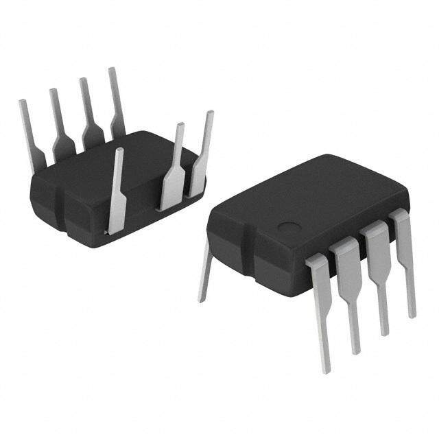
| 产品图片 |
|
| rohs | 符合RoHS无铅 / 符合限制有害物质指令(RoHS)规范要求 |
| 产品系列 | 电源管理 IC,开关控制器 ,Texas Instruments UCC3810N- |
| 数据手册 | |
| 产品型号 | UCC3810N |
| PWM类型 | 电流模式 |
| 上升时间 | 20 ns |
| 下降时间 | 30 ns |
| 产品目录页面 | |
| 产品种类 | 开关控制器 |
| 倍增器 | 无 |
| 其它名称 | 296-11491-5 |
| 分频器 | 无 |
| 包装 | 管件 |
| 升压 | 是 |
| 单位重量 | 1.054 g |
| 占空比 | 50% |
| 占空比-最大 | 50 % |
| 反向 | 无 |
| 反激式 | 是 |
| 商标 | Texas Instruments |
| 安装风格 | Through Hole |
| 封装 | Tube |
| 封装/外壳 | 16-DIP(0.300",7.62mm) |
| 封装/箱体 | PDIP-16 |
| 工作温度 | 0°C ~ 70°C |
| 工厂包装数量 | 25 |
| 开关频率 | 1000 kHz |
| 拓扑结构 | Buck, Boost, Flyback, Forward |
| 最大工作温度 | + 70 C |
| 最小工作温度 | 0 C |
| 标准包装 | 25 |
| 电压-电源 | 9.5 V ~ 10 V |
| 类型 | Current Mode PWM Controllers |
| 系列 | UCC3810 |
| 输出数 | 2 |
| 输出电流 | 1000 mA |
| 输出端数量 | 2 Output |
| 降压 | 是 |
| 隔离式 | 是 |
| 频率-最大值 | 1MHz |


- 商务部:美国ITC正式对集成电路等产品启动337调查
- 曝三星4nm工艺存在良率问题 高通将骁龙8 Gen1或转产台积电
- 太阳诱电将投资9.5亿元在常州建新厂生产MLCC 预计2023年完工
- 英特尔发布欧洲新工厂建设计划 深化IDM 2.0 战略
- 台积电先进制程称霸业界 有大客户加持明年业绩稳了
- 达到5530亿美元!SIA预计今年全球半导体销售额将创下新高
- 英特尔拟将自动驾驶子公司Mobileye上市 估值或超500亿美元
- 三星加码芯片和SET,合并消费电子和移动部门,撤换高东真等 CEO
- 三星电子宣布重大人事变动 还合并消费电子和移动部门
- 海关总署:前11个月进口集成电路产品价值2.52万亿元 增长14.8%

PDF Datasheet 数据手册内容提取
UCC2810 UCC3810 www.ti.com SLUS162D–FEBRUARY1999–REVISEDFEBRUARY2007 DUAL CHANNEL SYNCHRONIZED CURRENT-MODE PWM FEATURES DESCRIPTION • SingleOscillatorSynchronizesTwoPWMs The UCC3810 is a high-speed BiCMOS controller • 150-µAStartupSupplyCurrent integrating two synchronized pulse width modulators • 2-mAOperatingSupplyCurrent for use in off-line and dc-to-dc power supplies. The UCC3810 family provides perfect synchronization • Operationto1MHz between two PWMs by usin g the same oscillator. • InternalSoft-Start The oscillator’s sawtooth waveform can be used for • Full-CycleFaultRestart slopecompensationifrequired. • InternalLeading-EdgeBlankingoftheCurrent Using a toggle flip-flop to alternate between SenseSignal modulators, the UCC3810 ensures that one PWM does not slave, interfere, or otherwise affect the • 1-ATotemPoleOutputs other PWM. This toggle flip- flop also ensures that • 75-nsTypicalResponsefromCurrentSense each PWM is limited to 50% maximum duty cycle, toOutput insuring adequate off-time to reset magnetic • 1.5%ToleranceVoltageReference elements. This device contains many of the same elements of the UC3842 current mode controller N PACKAGE family, combined with the enhancements of the (TOP VIEW) UCC3802. This minimizes power supply parts count. Enhancements include leading edge blanking of the SYNC 1 16 VCC current sense signals, full cycle fault restart, CMOS CT 2 15 REF output drivers, and outputs which remain low even RT 3 14 ENABLE2 whenthesupplyvoltageisremoved. FB1 4 13 FB2 COMP1 5 12 COMP2 CS1 6 11 CS2 OUT1 7 10 OUT2 GND 8 9 PWRGND PW PACKAGE (TOP VIEW) SYNC 1 16 VCC CT 2 15 REF RT 3 14 ENABLE2 FB1 4 13 FB2 COMP1 5 12 COMP2 CS1 6 11 CS2 OUT1 7 10 OUT2 GND 8 9 PWRGND Pleasebeawarethatanimportantnoticeconcerningavailability,standardwarranty,anduseincriticalapplicationsofTexas Instrumentssemiconductorproductsanddisclaimerstheretoappearsattheendofthisdatasheet. PRODUCTIONDATAinformationiscurrentasofpublicationdate. Copyright©1999–2007,TexasInstrumentsIncorporated Products conform to specifications per the terms of the Texas Instruments standard warranty. Production processing does not necessarilyincludetestingofallparameters.
UCC2810 UCC3810 www.ti.com SLUS162D–FEBRUARY1999–REVISEDFEBRUARY2007 Thesedeviceshavelimitedbuilt-inESDprotection.Theleadsshouldbeshortedtogetherorthedeviceplacedinconductivefoam duringstorageorhandlingtopreventelectrostaticdamagetotheMOSgates. ORDERINGINFORMATION PACKAGEDDEVICES(1) T J SOP(DW) PDIP(N) –40°Cto85°C UCC2810DW(16) UCC2810N(16) 0°Cto70°C UCC3810DW(16) UCC3810N(16) (1) Allpackagesareavailabletapedandreeled(indicatedbytheRsuffixonthedevicetypee.g., UCC2810JR) ABSOLUTE MAXIMUM RATINGS overoperatingfree-airtemperaturerange(unlessotherwisenoted)(1)(2) UNIT V Supplyvoltage(3) 11V CC I Supplycurrent 20mA CC Outputpeakcurrent,OUT1,OUT2,5%dutycycle ±1A Outputenergy,OUT1,OUT2,capacitiveload20µJ 20µJ Analoginputs,FB1,FB2,CS1,CS2,SYNC –0.3to6.3V T Operatingjunctiontemperature 150°C J T Storagetemperaturerange –65to150°C stg Leadtemperature(soldering,10sec) 300°C (1) Currentsarepositiveinto,negativeoutofthespecifiedterminal.AllvoltagesarewithrespecttoGND. (2) Stressesbeyondthoselistedunderabsolutemaximumratingsmaycausepermanentdamagetothedevice.Thesearestressratings only,andfunctionaloperationofthedeviceattheseoranyotherconditionsbeyondthoseindicatedunderrecommendedoperating conditionsisnotimplied.Exposuretoabsolute-maximum-ratedconditionsforextendedperiodsmayaffectdevicereliability. (3) Innormaloperation,V ispoweredthroughacurrent-limitingresistor.Absolutemaximumof11Vapplieswhendrivenfromalow CC impedancesuchthattheV currentdoesnotexceed20mA. CC BLOCKDIAGRAM REF FB1 COMP1 CS1 CS2 VCC 15 15 5 6 11 16 Over-Current Comparator Leading Leading 12.5 V Edge Edge 1.5 V Blanking Blanking VCC OK VCC 2.5E Vrror S Q 7 OUT1 Amp 1 55 k(cid:1) Voltage R Ref REF OK S Q 100 k(cid:1) 1 V R Error 4 V Amp 2 S Q 10 OUT2 0.5 V R 2.5 V + S Q Full Cycle − R Soft Start R 35 (cid:2)A 55 k(cid:1) 2 t − 5ms 100 k(cid:1) 1 V Oscillator 13 12 1 2 3 14 9 8 FB2 COMP2 SYNC CT RT ENABLES PWRGND GND VDG−92062−1 2 SubmitDocumentationFeedback
UCC2810 UCC3810 www.ti.com SLUS162D–FEBRUARY1999–REVISEDFEBRUARY2007 ELECTRICAL CHARACTERISTICS Allparametersarethesameforbothchannels,–40°C£ T £ 85°CfortheUCC2810,0°C£ T £ 70°CfortheUCC3810, A A V =10V(1);R =150kW ,C =120pF;noload;T =T (unlessotherwisespecified) CC T T A J; PARAMETER TESTCONDITIONS MIN TYP MAX UNIT REFERENCE T =25°C 4.925 5.000 5.075 J V Outputvoltage V CC T =fullrange,0mA£ I £ 5mA 4.85 5.00 5.10 J REF Loadregulation 0mA£ I £ 5mA 5 30 REF UVLOstopthresholdvoltage, 12 mV Lineregulation 0.5V£ V £ V CC SHUNT Outputnoisevoltage(2) 10Hz<f<10kHz, T =25°C 235 µV J Longtermstability(2) TA=125°C, 1000hours 5 mV I Outputshortcircuitcurrent -8 -25 mA O(SC) OSCILLATOR R =30kW , C =120pF 860 980 1100 f Oscillatorfrequency(3) T T kHz OSC R =150kW , C =120pF 190 220 250 T T Temperaturestability(2) 2.5% Peakvoltage 2.5 Valleyvoltage 0.05 V Peak-to-peakamplitude 2.25 2.45 2.65 SYNCthresholdvoltage 0.80 1.65 2.20 SYNCinputcurrent SYNC=5V 30 µA ERRORAMPLIFIER V FBinputvoltage COMP=2.5V 2.44 2.50 2.56 V FB I FBinputbiascurrent ±1 µA FB Openloopvoltagegain 60 73 dB f Unitygainbandwidth(2) 2 MHz GAIN I Sinkcurrent,COMP FB=2.7V, COMP=1V 0.3 1.4 3.5 SINK I Sourcecurrent,COMP FB=1.8V, COMP=4V -0.2 -0.5 -0.8 mA SRCE Minimumdutycycle COMP=0V 0% FB=1.8V, 5 Soft-startrisetime,COMP ms Risefrom0.5Vto(REF–1.5V) CURRENTSENSE Gain(4) 1.20 1.55 1.80 V/V Maximuminputsignal(5) COMP=5V 0.9 1.0 1.1 V I Inputbiascurrent,CS ±200 nA CS CSstepsfrom0Vto1.2V, 75 Propagationdelaytime(CStoOUT) COMP=2.5V ns Blanktime,CS(6) 55 Overcurrentthresholdvoltage,CS 1.35 1.55 1.85 V COMP-to-CSoffsetvoltage CS=0V 0.45 0.90 1.35 (1) ForUCC3810,adjustV abovethestartthresholdbeforesettingat10V. CC (2) Ensuredbydesign.Notproductiontested. 4 f = OSC R ´C (3) Oscillatorfrequencyistwicetheoutputfrequency. T T DV A= COMP DV (4) CurrentsensegainAisdefinedby: CS ,0V£ V £ 0.8V. CS (5) ParametermeasuredattrippointoflatchwithFB=0V. (6) CSblanktimeismeasuredasthedifferencebetweentheminimumnon-zeroon-timeandtheCS-to-OUTdelay. SubmitDocumentationFeedback 3
UCC2810 UCC3810 www.ti.com SLUS162D–FEBRUARY1999–REVISEDFEBRUARY2007 ELECTRICAL CHARACTERISTICS (continued) Allparametersarethesameforbothchannels,–40°C£ T £ 85°CfortheUCC2810,0°C£ T £ 70°CfortheUCC3810, A A V =10V;R =150kW ,C =120pF;noload;T =T (unlessotherwisespecified) CC T T A J; PARAMETER TESTCONDITIONS MIN TYP MAX UNIT PWM R =150kW , C =120pF 45% 49% 50% Maximumdutycycle(2) T T R =30kW , C =120pF 40% 45% 48% T T Minimumon-time CS=1.2V, COMP=5V 130 ns OUTPUT I =20mA 0.12 0.42 OUT V Low-leveloutputvoltage I =200mA 0.48 1.10 OL OUT I =20mA, V =0V 0.7 1.2 V OUT CC I =–20mA 0.15 0.42 OUT V High-leveloutputvoltage(V –OUT) OH CC I =–200mA 1.2 2.3 OUT t Risetime,OUT C =1nF 20 50 R OUT ns t Falltime,OUT C =1nF 30 60 F OUT UNDERVOLTAGELOCKOUT(UVLO) Startthresholdvoltage 9.6 11.3 13.2 Stopthresholdvoltage 7.1 8.3 9.5 V Start-to-stophysteresis 1.7 3.0 4.7 ENABLE2inputbiascurrent ENABLE2=0V -20 -35 -55 µA ENABLE2inputthresholdvoltage 0.80 1.53 2.00 V OVERALL Startupcurrent V <Startthresholdvoltage 0.15 0.25 CC Operatingsupplycurrent,outputsoff VCC=10V, FB=2.75V 2 3 VCC=10V, FB=0V, 3.2 5.1 mA CS=0V, RT=150kW Operatingsupplycurrent,outputson VCC=10V, FB=0V, 8.5 14.5 CS=0V, RT=30kW VCCinternalzenervoltage I =10mA 11.0 12.9 14.0 CC VCCinternalzenervoltageminusstart 0.4 1.2 V thresholdvoltage 4 SubmitDocumentationFeedback
UCC2810 UCC3810 www.ti.com SLUS162D–FEBRUARY1999–REVISEDFEBRUARY2007 DEVICE INFORMATION TERMINALFUNCTIONS TERMINAL I/O DESCRIPTION NAME NO. COMP1 5 O Lowimpedanceoutputoftheerroramplifiers. COMP2 12 O CS1 6 I CurrentsenseinputstothePWMcomparators.Theseinputshaveleadingedgeblanking.For mostapplications,noinputfilteringisrequired.LeadingedgeblankingdisconnectstheCSinputs fromallinternalcircuitsforthefirst55nsofeachPWMcycle.Whenusedwithveryslowdiodesor CS2 11 I inotherapplicationswherethecurrentsensesignalisunusuallynoisy,asmallcurrent-senseR-C filtermayberequired. Thetimingcapacitoroftheoscillator.RecommendedvaluesofCTarebetween100pFand1nF. CT 2 O ConnectthetimingcapacitordirectlyacrossCTandGND. AlogicinputwhichdisablesPWM2whenlow.ThisinputhasnoeffectonPWM1.Thisinputis internallypulledhigh.Inmostapplicationsitcanbeleftfloating.Inunusuallynoisyapplications, ENABLE2 14 I theinputshouldbebypassedwitha1-nFceramiccapacitor.ThisinputhasTTLcompatible thresholds. FB1 4 I Thehighimpedanceinvertinginputsoftheerroramplifiers. FB2 13 I Toseparatenoisefromthecriticalcontrolcircuits,thisparthastwodifferentgroundconnections: GND 8 – GNDandPWRGND.GNDandPWRGNDmustbeelectricallyconnectedtogether.However,use caretoavoidcouplingnoiseintoGND. OUT1 7 O Thehigh-currentpush-pulloutputsofthePWMareintendedtodrivepowerMOSFETgates throughasmallresistor.Thisresistoractsasbothacurrentlimitingresistorandasadamping OUT2 10 O impedancetominimizeringingandovershoot. Toseparatenoisefromthecriticalcontrolcircuits,thisparthastwodifferentgroundconnections: PWRGND 9 – GNDandPWRGND.GNDandPWRGNDmustbeelectricallyconnectedtogether. Theoutputofthe5-Vreference.BypassREFtoGNDwithaceramiccapacitor‡ 0.01-µFforbest REF 15 O performance. TheoscillatorchargingcurrentissetbythevalueoftheresistorconnectedfromRTtoGND.This pinisregulatedto1V,buttheactualchargingcurrentis10V/RT.RecommendedvaluesofRT RT 3 O arebetween10kW and470kW .Foragivenfrequency,highertimingresistorsgivehigher maximumdutycycleandslightlyloweroverallpowerconsumption. Thislogicinputcanbeusedtosynchronizetheoscillatortoafreerunningoscillatorinanother SYNC 1 I part.ThispinisedgetriggeredwithTTLthresholds,andrequiresatleasta10-ns-widepulse.If unused,thispincanbegrounded,opencircuited,orconnectedtoREF. Thepowerinputtothedevice.Thispinsuppliescurrenttoallfunctionsincludingthehighcurrent VCC 16 I outputstagesandtheprecisionreference.Therefore,itiscriticalthatVCCbedirectlybypassedto PWRGNDwithan0.1-µFceramiccapacitor. SubmitDocumentationFeedback 5
UCC2810 UCC3810 www.ti.com SLUS162D–FEBRUARY1999–REVISEDFEBRUARY2007 APPLICATION INFORMATION TIMING RESISTOR SupplycurrentdecreaseswithincreasedR bytherelationship: T 11V DI = CC R T Formoreinformation,seethedetailedoscillatorblockdiagram. LEADING EDGE BLANKING AND CURRENT SENSE Figure 1 shows how an external power stage is connected to the UCC3810. The gate of an external power N-channel MOSFET is connected to OUT through a small current-limiting resistor. For most applications, a 10-W resistor is adequate to limit peak current and also practical at damping resonances between the gate driver and the MOSFET input reactance. Long gate lead length increases gate capacitance and mandates a higher series gate resistor to damp the R-L-C tank formed by the lead, the MOSFET input reactance, and the device’s driver outputresistance. The UCC3810 features internal leading edge blanking of the current-sense signal on both current sense inputs. The blank time starts when OUT rises and continues for 55 ns. During that 55 ns period, the signal on CS is ignored. For most PWM applications, this means that the CS input can be connected to the current-sense resistor as shown in Figure 1. However, high speed grounding practices and short lead lengths are still required forgoodperformance. From Over−Current Oscillator S Comparator 1.5 V − Soft R Q Power Start + OUT Stage Gate Driver + CS R − Current + PWM PWM Sense − Comparator Latch Resistor One Error Shot Amp Figure1.DetailedBlockDiagram OSCILLATOR The UCC3810 oscillator generates a sawtooth wave at CT. The sawtooth rise time is set by the resistor from RT to GND. Since R is biased at 1 V, the current through R is 1 V/R . The actual charging current is 10 times T T T higher. The fall time is set by an internal transistor on-resistance of approximately 100 W . During the fall time, all outputs are off and the maximum duty cycle is reduced to below 50%. Larger timing capacitors increase the discharge time and reduce frequency. However, the percentage maximum duty cycle is only a function of the timingresistorR ,andtheinternal100-W dischargeresistance. T ERROR AMPLIFIER OUTPUT STAGE The UCC3810 error amplifiers are operational amplifiers with low-output resistance and high-input resistance. The output stage of one error amplifier is shown in Figure 3. This output stage allows the error amplifier output toswingclosetoGNDandashighasonediodedropbelow5Vwithlittlelossinamplifierperformance. 6 SubmitDocumentationFeedback
UCC2810 UCC3810 www.ti.com SLUS162D–FEBRUARY1999–REVISEDFEBRUARY2007 APPLICATION INFORMATION (continued) VCC 0.2 V + − I 10I R Q 1 V + + − RON (cid:1) 100 2.5 V − S One Shot 3 2 1 RT SYNC RT CT Figure2.Oscillator 5 V VCC COMP Figure3.ErrorAmplifierOutputStage SubmitDocumentationFeedback 7
UCC2810 UCC3810 www.ti.com SLUS162D–FEBRUARY1999–REVISEDFEBRUARY2007 TYPICAL CHARACTERISTICS ERRORAMPLIFERGAINANDPHASE OSCILLATORFREQUENCY vs vs FREQUENCY TIMINGRESISTANCE 80 1 M 60 135 z H − Fhase y B 40 90 nc d e Gain − 20 Gain 45 °hase − ator Frequ 100 k P cill s O 0 0 −20 10 k 1 k 10 k 100 k 1 M 10 M 10 k 100 k 10 M f − Frequency − Hz RT − Timing Resistor − (cid:1) Figure4. Figure5. OSCILLATORFREQUENCY MAXIMUMDUTYCYCLE vs vs TEMPERATURE TIMINGRESISTANCE 1.2 50 1.15 48 Hz 1.1 M − cy 1.05 % uen e − 46 Freq 1 Cycl ator 0.95 Duty 44 cill s O 0.9 42 0.85 0.8 40 −55 −35 −15 5 25 45 65 85 105 125 10 k 100 k 1 M TA − Temperature − (cid:2)C RT − Timing Resistor − (cid:1) Figure6. Figure7. 8 SubmitDocumentationFeedback
UCC2810 UCC3810 www.ti.com SLUS162D–FEBRUARY1999–REVISEDFEBRUARY2007 TYPICAL CHARACTERISTICS (continued) INPUTCURRENT MAXIMUMDUTYCYCLE vs vs OSCILLATORFREQUENCY FREQUENCY 10 50 8 48 A m − ent 6 − % 46 Curr ycle nput 4 Switching uty C 44 − I D C C I 2 42 Outputs Off CT = 120 pF 40 10 k 100 k 1 M 10 k 100 k 1 M f − Frequency − Hz f − Frequency − Hz Figure8. Figure9. DC +12 V OUT Input +5 V OUT 0.1 (cid:1)F 16 OPTO1 VCC 2 3 5 COMP1 COMP VCC OUT1 7 5 REF 0.1 OPTO1 4 FB1 COLL 1 UCC3810 4 E/A+ OPTO2 12 COMP2 CS1 6 0.1 6 SENSEISET 8 OUT2 10 UC39432GND 7 13 FB2 TTL MONITOR CS2 11 High Voltage Out SYNC 1 SYNC (Monitor Raster) REF 15 HV SUP 14 ENABLE2 ENABLE PWR RT CT GND GND 0.1 3 2 8 9 2 3 COMP VCC 0.1 OPTO2 5 REF COLL 1 4 E/A+ 0.1 6 SENSEISET 8 GND UC39432 7 VDG−94022 Figure10.TypicalApplication SubmitDocumentationFeedback 9
PACKAGE MATERIALS INFORMATION www.ti.com 26-Mar-2013 TAPE AND REEL INFORMATION *Alldimensionsarenominal Device Package Package Pins SPQ Reel Reel A0 B0 K0 P1 W Pin1 Type Drawing Diameter Width (mm) (mm) (mm) (mm) (mm) Quadrant (mm) W1(mm) UCC3810DWTR SOIC DW 16 2000 330.0 16.4 10.75 10.7 2.7 12.0 16.0 Q1 PackMaterials-Page1
PACKAGE MATERIALS INFORMATION www.ti.com 26-Mar-2013 *Alldimensionsarenominal Device PackageType PackageDrawing Pins SPQ Length(mm) Width(mm) Height(mm) UCC3810DWTR SOIC DW 16 2000 367.0 367.0 38.0 PackMaterials-Page2
IMPORTANTNOTICE TexasInstrumentsIncorporatedanditssubsidiaries(TI)reservetherighttomakecorrections,enhancements,improvementsandother changestoitssemiconductorproductsandservicesperJESD46,latestissue,andtodiscontinueanyproductorserviceperJESD48,latest issue.Buyersshouldobtainthelatestrelevantinformationbeforeplacingordersandshouldverifythatsuchinformationiscurrentand complete.Allsemiconductorproducts(alsoreferredtohereinas“components”)aresoldsubjecttoTI’stermsandconditionsofsale suppliedatthetimeoforderacknowledgment. TIwarrantsperformanceofitscomponentstothespecificationsapplicableatthetimeofsale,inaccordancewiththewarrantyinTI’sterms andconditionsofsaleofsemiconductorproducts.TestingandotherqualitycontroltechniquesareusedtotheextentTIdeemsnecessary tosupportthiswarranty.Exceptwheremandatedbyapplicablelaw,testingofallparametersofeachcomponentisnotnecessarily performed. TIassumesnoliabilityforapplicationsassistanceorthedesignofBuyers’products.Buyersareresponsiblefortheirproductsand applicationsusingTIcomponents.TominimizetherisksassociatedwithBuyers’productsandapplications,Buyersshouldprovide adequatedesignandoperatingsafeguards. TIdoesnotwarrantorrepresentthatanylicense,eitherexpressorimplied,isgrantedunderanypatentright,copyright,maskworkright,or otherintellectualpropertyrightrelatingtoanycombination,machine,orprocessinwhichTIcomponentsorservicesareused.Information publishedbyTIregardingthird-partyproductsorservicesdoesnotconstitutealicensetousesuchproductsorservicesorawarrantyor endorsementthereof.Useofsuchinformationmayrequirealicensefromathirdpartyunderthepatentsorotherintellectualpropertyofthe thirdparty,oralicensefromTIunderthepatentsorotherintellectualpropertyofTI. ReproductionofsignificantportionsofTIinformationinTIdatabooksordatasheetsispermissibleonlyifreproductioniswithoutalteration andisaccompaniedbyallassociatedwarranties,conditions,limitations,andnotices.TIisnotresponsibleorliableforsuchaltered documentation.Informationofthirdpartiesmaybesubjecttoadditionalrestrictions. ResaleofTIcomponentsorserviceswithstatementsdifferentfromorbeyondtheparametersstatedbyTIforthatcomponentorservice voidsallexpressandanyimpliedwarrantiesfortheassociatedTIcomponentorserviceandisanunfairanddeceptivebusinesspractice. TIisnotresponsibleorliableforanysuchstatements. Buyeracknowledgesandagreesthatitissolelyresponsibleforcompliancewithalllegal,regulatoryandsafety-relatedrequirements concerningitsproducts,andanyuseofTIcomponentsinitsapplications,notwithstandinganyapplications-relatedinformationorsupport thatmaybeprovidedbyTI.Buyerrepresentsandagreesthatithasallthenecessaryexpertisetocreateandimplementsafeguardswhich anticipatedangerousconsequencesoffailures,monitorfailuresandtheirconsequences,lessenthelikelihoodoffailuresthatmightcause harmandtakeappropriateremedialactions.BuyerwillfullyindemnifyTIanditsrepresentativesagainstanydamagesarisingoutoftheuse ofanyTIcomponentsinsafety-criticalapplications. Insomecases,TIcomponentsmaybepromotedspecificallytofacilitatesafety-relatedapplications.Withsuchcomponents,TI’sgoalisto helpenablecustomerstodesignandcreatetheirownend-productsolutionsthatmeetapplicablefunctionalsafetystandardsand requirements.Nonetheless,suchcomponentsaresubjecttotheseterms. NoTIcomponentsareauthorizedforuseinFDAClassIII(orsimilarlife-criticalmedicalequipment)unlessauthorizedofficersoftheparties haveexecutedaspecialagreementspecificallygoverningsuchuse. OnlythoseTIcomponentswhichTIhasspecificallydesignatedasmilitarygradeor“enhancedplastic”aredesignedandintendedforusein military/aerospaceapplicationsorenvironments.BuyeracknowledgesandagreesthatanymilitaryoraerospaceuseofTIcomponents whichhavenotbeensodesignatedissolelyattheBuyer'srisk,andthatBuyerissolelyresponsibleforcompliancewithalllegaland regulatoryrequirementsinconnectionwithsuchuse. TIhasspecificallydesignatedcertaincomponentsasmeetingISO/TS16949requirements,mainlyforautomotiveuse.Inanycaseofuseof non-designatedproducts,TIwillnotberesponsibleforanyfailuretomeetISO/TS16949. Products Applications Audio www.ti.com/audio AutomotiveandTransportation www.ti.com/automotive Amplifiers amplifier.ti.com CommunicationsandTelecom www.ti.com/communications DataConverters dataconverter.ti.com ComputersandPeripherals www.ti.com/computers DLP®Products www.dlp.com ConsumerElectronics www.ti.com/consumer-apps DSP dsp.ti.com EnergyandLighting www.ti.com/energy ClocksandTimers www.ti.com/clocks Industrial www.ti.com/industrial Interface interface.ti.com Medical www.ti.com/medical Logic logic.ti.com Security www.ti.com/security PowerMgmt power.ti.com Space,AvionicsandDefense www.ti.com/space-avionics-defense Microcontrollers microcontroller.ti.com VideoandImaging www.ti.com/video RFID www.ti-rfid.com OMAPApplicationsProcessors www.ti.com/omap TIE2ECommunity e2e.ti.com WirelessConnectivity www.ti.com/wirelessconnectivity MailingAddress:TexasInstruments,PostOfficeBox655303,Dallas,Texas75265 Copyright©2013,TexasInstrumentsIncorporated