ICGOO在线商城 > 集成电路(IC) > PMIC - AC-DC 转换器,离线开关 > FSCQ0965RTYDTU
 Datasheet下载
- 型号: FSCQ0965RTYDTU
- 制造商: Fairchild Semiconductor
- 库位|库存: xxxx|xxxx
- 要求:
| 数量阶梯 | 香港交货 | 国内含税 |
| +xxxx | $xxxx | ¥xxxx |
查看当月历史价格
查看今年历史价格
FSCQ0965RTYDTU产品简介:
ICGOO电子元器件商城为您提供FSCQ0965RTYDTU由Fairchild Semiconductor设计生产,在icgoo商城现货销售,并且可以通过原厂、代理商等渠道进行代购。 FSCQ0965RTYDTU价格参考¥19.62-¥35.50。Fairchild SemiconductorFSCQ0965RTYDTU封装/规格:PMIC - AC-DC 转换器,离线开关, Converter Offline Flyback Topology 20kHz TO-220F-5L (Forming)。您可以下载FSCQ0965RTYDTU参考资料、Datasheet数据手册功能说明书,资料中有FSCQ0965RTYDTU 详细功能的应用电路图电压和使用方法及教程。
FSCQ0965RTYDTU 是 ON Semiconductor(现为安森美半导体)推出的一款 PMIC - AC-DC 转换器,属于离线开关系列。该型号主要应用于需要高效、可靠且紧凑的电源解决方案的场景。以下是其典型应用场景:

1. 消费类电子产品
   适用于电视、机顶盒、音响设备、家用电器等需要将交流电转换为直流电的设备。它能够提供稳定的电压输出,支持低待机功耗设计,满足现代家电对能效的要求。

2. 充电器和适配器
   用于手机充电器、笔记本电脑适配器以及其他便携式电子设备的电源适配器中。其高效的功率转换能力可以减少发热,同时支持快速充电功能。

3. 工业控制与自动化
   在工业领域中,可用于 PLC(可编程逻辑控制器)、传感器接口模块以及小型电机驱动器的电源供应部分。高可靠性和宽输入电压范围使其适合复杂的工业环境。

4. 物联网 (IoT) 设备
   针对智能家居、智能照明及无线通信节点等 IoT 应用,该芯片提供的小尺寸封装和高效性能有助于实现紧凑型设计,并延长电池寿命或降低运行成本。

5. 医疗设备
   对于便携式健康监测仪、血压计、血糖仪等低功耗医疗仪器来说,这款 AC-DC 转换器可以确保精准供电并符合严格的安规标准。

6. LED 照明系统
   在 LED 驱动电源中使用,以提高效率和调光兼容性,同时保持较低的成本结构。特别适合室内/室外灯具、筒灯和面板灯等应用。

总之,FSCQ0965RTYDTU 凭借其先进的技术特性,如高集成度、低功耗、良好的电磁兼容性(EMC),广泛适用于各种需要稳定直流电源输出的场合。
| 参数 | 数值 |
| 产品目录 | 集成电路 (IC)半导体 |
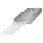
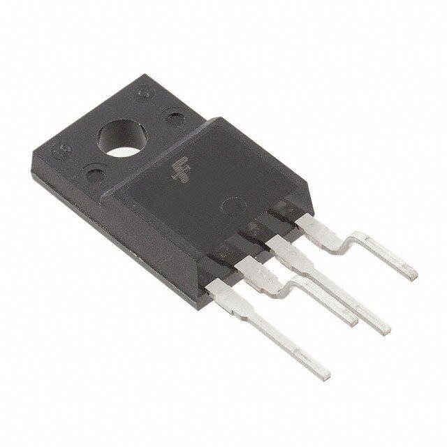
| 描述 | IC FPS PWM SWITCH 650V TO-220F-5交流/直流转换器 POWER CONVERSION |
| 产品分类 | |
| 品牌 | Fairchild Semiconductor |
| 产品手册 | |
| 产品图片 |
|
| rohs | RoHS 合规性豁免无铅 / 符合限制有害物质指令(RoHS)规范要求 |
| 产品系列 | 电源管理 IC,交流/直流转换器,Fairchild Semiconductor FSCQ0965RTYDTUFPS™ |
| 数据手册 | |
| 产品型号 | FSCQ0965RTYDTU |
| PCN封装 | |
| 产品种类 | 交流/直流转换器 |
| 供应商器件封装 | TO-220F-5L(成形) |
| 功率(W) | 130W |
| 包装 | 管件 |
| 单位重量 | 2.894 g |
| 商标 | Fairchild Semiconductor |
| 安装风格 | Through Hole |
| 封装 | Tube |
| 封装/外壳 | TO-220-5 全封装(成形引线) |
| 封装/箱体 | TO-220-5 FP |
| 工作温度 | -25°C ~ 85°C |
| 工作温度范围 | - 25 C to + 85 C |
| 工厂包装数量 | 400 |
| 开关频率 | 20 kHz |
| 标准包装 | 50 |
| 电压-击穿 | 650V |
| 电压-输入 | 9 V ~ 20 V |
| 电压-输出 | - |
| 电源电流 | 6 mA |
| 系列 | FSCQ0965RT |
| 输出电压 | 650 V |
| 输出电流 | 5.28 A |
| 输出端数量 | 1 Output |
| 输出隔离 | 隔离 |
| 零件号别名 | FSCQ0965RTYDTU_NL |
| 频率范围 | 18kHz ~ 22kHz |


- 商务部:美国ITC正式对集成电路等产品启动337调查
- 曝三星4nm工艺存在良率问题 高通将骁龙8 Gen1或转产台积电
- 太阳诱电将投资9.5亿元在常州建新厂生产MLCC 预计2023年完工
- 英特尔发布欧洲新工厂建设计划 深化IDM 2.0 战略
- 台积电先进制程称霸业界 有大客户加持明年业绩稳了
- 达到5530亿美元!SIA预计今年全球半导体销售额将创下新高
- 英特尔拟将自动驾驶子公司Mobileye上市 估值或超500亿美元
- 三星加码芯片和SET,合并消费电子和移动部门,撤换高东真等 CEO
- 三星电子宣布重大人事变动 还合并消费电子和移动部门
- 海关总署:前11个月进口集成电路产品价值2.52万亿元 增长14.8%


PDF Datasheet 数据手册内容提取
Is Now Part of To learn more about ON Semiconductor, please visit our website at www.onsemi.com Please note: As part of the Fairchild Semiconductor integration, some of the Fairchild orderable part numbers will need to change in order to meet ON Semiconductor’s system requirements. Since the ON Semiconductor product management systems do not have the ability to manage part nomenclature that utilizes an underscore (_), the underscore (_) in the Fairchild part numbers will be changed to a dash (-). This document may contain device numbers with an underscore (_). Please check the ON Semiconductor website to verify the updated device numbers. The most current and up-to-date ordering information can be found at www.onsemi.com. Please email any questions regarding the system integration to Fairchild_questions@onsemi.com. ON Semiconductor and the ON Semiconductor logo are trademarks of Semiconductor Components Industries, LLC dba ON Semiconductor or its subsidiaries in the United States and/or other countries. ON Semiconductor owns the rights to a number of patents, trademarks, copyrights, trade secrets, and other intellectual property. A listing of ON Semiconductor’s product/patent coverage may be accessed at www.onsemi.com/site/pdf/Patent-Marking.pdf. ON Semiconductor reserves the right to make changes without further notice to any products herein. ON Semiconductor makes no warranty, representation or guarantee regarding the suitability of its products for any particular purpose, nor does ON Semiconductor assume any liability arising out of the application or use of any product or circuit, and specifically disclaims any and all liability, including without limitation special, consequential or incidental damages. Buyer is responsible for its products and applications using ON Semiconductor products, including compliance with all laws, regulations and safety requirements or standards, regardless of any support or applications information provided by ON Semiconductor. “Typical” parameters which may be provided in ON Semiconductor data sheets and/or specifications can and do vary in different applications and actual performance may vary over time. All operating parameters, including “Typicals” must be validated for each customer application by customer’s technical experts. ON Semiconductor does not convey any license under its patent rights nor the rights of others. ON Semiconductor products are not designed, intended, or authorized for use as a critical component in life support systems or any FDA Class 3 medical devices or medical devices with a same or similar classification in a foreign jurisdiction or any devices intended for implantation in the human body. Should Buyer purchase or use ON Semiconductor products for any such unintended or unauthorized application, Buyer shall indemnify and hold ON Semiconductor and its officers, employees, subsidiaries, affiliates, and distributors harmless against all claims, costs, damages, and expenses, and reasonable attorney fees arising out of, directly or indirectly, any claim of personal injury or death associated with such unintended or unauthorized use, even if such claim alleges that ON Semiconductor was negligent regarding the design or manufacture of the part. ON Semiconductor is an Equal Opportunity/Affirmative Action Employer. This literature is subject to all applicable copyright laws and is not for resale in any manner.
F S C Q - January 2014 S e r i e s — FSCQ-Series: G r FSCQ0565RT / FSCQ0765RT / FSCQ0965RT / FSCQ1265RT / FSCQ1565RT e e Green Mode Fairchild Power Switch (FPS™) n M o d e Features Description F a i r Optimized for Quasi-Resonant Converter (QRC) A Quasi-Resonant Converter (QRC) typically shows c h lower EMI and higher power conversion efficiency Advanced Burst-Mode Operation for under 1 W compared to a conventional hard-switched converter ild Standby Power Consumption with a fixed switching frequency. Therefore, a QRC is P Pulse-by-Pulse Current Limit well suited for noise-sensitive applications, such as ow color TV and audio. Each product in the FSCQ series Overload Protection (OLP) – Auto Restart contains an integrated Pulse Width Modulation (PWM) er Over-Voltage Protection (OVP) – Auto Restart controller and a SenseFET. This series is specifically S w designed for quasi-resonant off-line Switch Mode Power Abnormal Over-Current Protection (AOCP) – Latch Supplies (SMPS) with minimal external components. itc Internal Thermal Shutdown (TSD) – Latch The PWM controller includes an integrated fixed h frequency oscillator, under-voltage lockout, leading- ( F Under-Voltage Lockout (UVLO) with Hysteresis edge blanking (LEB), optimized gate driver, internal soft- P Low Startup Current (Typical: 25 μA) start, temperature-compensated precise current sources S™ for loop compensation, and self-protection circuitry. Internal High Voltage SenseFET Compared with a discrete MOSFET and PWM controller ) Built-in Soft-Start (20 ms) solution, the FSCQ series can reduce total cost, component count, size, and weight; while increasing Extended Quasi-Resonant Switching efficiency, productivity, and system reliability. These devices provide a basic platform for cost-effective Applications designs of quasi-resonant switching flyback converters. CTV Audio Amplifier Related Resources AN-4146 — Design Guidelines for Quasi-Resonant Converters Using FSCQ-Series Fairchild Power Switch AN-4140 — Transformer Design Consideration for Offline Flyback Converters Using Fairchild Power Switch Ordering Information Part Number Package Marking Code BV (V) R Max. (Ω) DSS DSON FSCQ0565RTYDTU TO-220F-5L (Forming) CQ0565RT 650 2.2 FSCQ0765RTYDTU TO-220F-5L (Forming) CQ0765RT 650 1.6 FSCQ0965RTYDTU TO-220F-5L (Forming) CQ0965RT 650 1.2 FSCQ1265RTYDTU TO-220F-5L (Forming) CQ1265RT 650 0.9 FSCQ1565RTYDTU TO-220F-5L (Forming) CQ1565RT 650 0.7 © 2006 Fairchild Semiconductor Corporation www.fairchildsemi.com FSQ-Series • Rev. 1.1.3
F S C Typical Circuit Q - S V e O r i e s — G r e e AC n M IN o d e F Drain a FSCQ-Series ir c h PWM il d Sync GND P o w e r V V FB CC S w i t c h ( F P S ™ ) Figure 1. Typical Flyback Application Table 1. Maximum Output Power(1) 230 V ±15%(2) 85–265 V AC AC Product Open Frame(3) Open Frame(3) FSCQ0565RT 70 W 60 W FSCQ0765RT 100 W 85 W FSCQ0965RT 130 W 110 W FSCQ1265RT 170 W 140 W FSCQ1565RT 210 W 170 W Notes: 1. The junction temperature can limit the maximum output power. 2. 230 V or 100/115 V with doubler. AC AC 3. Maximum practical continuous power in an open frame design at 50C ambient. © 2006 Fairchild Semiconductor Corporation www.fairchildsemi.com FSQ-Series • Rev. 1.1.3 2
F S C Internal Block Diagram Q - S Sync Vcc Drain e 5 3 1 ri e + s Q(QuRas) iS-Rweistcohnianngt fs + — Threshold - Controller - 9V/15V G Soft Start r 4.6V/2.6V : Normal QR e 3.0V/1.8V : Extended QR Vcc good e n Burst Mode Auxiliary M V Controller OSC Vref Main Bias o Burst d e Normal Operation Burst Switching Normal F Vref Vref Vref Operation Internal a i Bias r IBFB IFB IB c Vcc h i l VFB Idelay PWM S Q d P 4 o 2.5R Gate w R Q e R Driver r LEB S w 600ns VSD itc h Sync S Q AOCP (F Vovp Vcc good Q S P R Q 2 GND S (Vcc = 9V) ™ Q R TSD Vocp ) Power Off Reset (Vcc = 6V) Figure 2. Functional Block Diagram © 2006 Fairchild Semiconductor Corporation www.fairchildsemi.com FSQ-Series • Rev. 1.1.3 3
F S C Pin Configuration Q - S e r i 5 SYNC e s — 4 VFB G 3 VCC re e n 2 GND M o d e F 1 DRAIN a i r c Figure 3. Pin Assignments (Top View) h i l d P o w e r S Pin Descriptions w i t c Pin Name Description h ( 1 DRAIN This pin is the high-voltage power SenseFET drain connection. F P 2 GND This pin is the control ground and the SenseFET source. S ™ 3 VCC This pin is the positive supply input. This pin provides internal operating current for both startup ) and steady-state operation. This pin is internally connected to the inverting input of the PWM comparator. The collector of an opto-coupler is typically tied to this pin. For stable operation, a capacitor should be placed 4 VFB between this pin and GND. If the voltage of this pin reaches 7.5 V, the overload protection triggers, which results in the FPS™ shutting down. This pin is internally connected to the sync detect comparator for quasi-resonant switching. In 5 SYNC normal quasi-resonant operation, the threshold of the sync comparator is 4.6 V / 2.6 V. Whereas, the sync threshold is changed to 3.0 V / 1.8 V in an extended quasi-resonant operation. © 2006 Fairchild Semiconductor Corporation www.fairchildsemi.com FSQ-Series • Rev. 1.1.3 4
F S C Absolute Maximum Ratings Q - Stresses exceeding the absolute maximum ratings may damage the device. The device may not function or be S e operable above the recommended operating conditions and stressing the parts to these levels is not recommended. r In addition, extended exposure to stresses above the recommended operating conditions may affect device reliability. ie s The absolute maximum ratings are stress ratings only. T = 25°C, unless otherwise specified. A — Symbol Parameter Value Unit G VDS Drain Pin Voltage 650 V re e VCC Supply Voltage 20 V n V -0.3 to 13 M sync Analog Input Voltage Range V o V -0.3 to V d FB CC e FSCQ0565RT 11.2 F a FSCQ0765RT 15.2 i r c IDM Drain Current Pulsed(4) FSCQ0965RT 16.4 A h i l FSCQ1265RT 21.2 d P FSCQ1565RT 26.4 o w FSCQ0565RT 2.8 e FSCQ0765RT 3.8 r S Continuous Drain Current (T = 25°C) I C FSCQ0965RT 4.1 A w D (TC: Case Back Surface Temperature) (rms) it FSCQ1265RT 5.3 c h FSCQ1565RT 6.6 ( F FSCQ0565RT 5.0 P S FSCQ0765RT 7.0 ™ Continuous Drain Current* (T = 25°C) ID* (T : Drain Lead TemperatureD)L FSCQ0965RT 7.6 A(rms) ) DL FSCQ1265RT 11.0 FSCQ1565RT 13.3 FSCQ0565RT 1.7 FSCQ0765RT 2.4 I Continuous Drain Current (T = 100°C) FSCQ0965RT 2.6 A D C (rms) FSCQ1265RT 3.4 FSCQ1565RT 4.4 FSCQ0565RT 400 FSCQ0765RT 570 E Single-Pulsed Avalanche Energy(5) FSCQ0965RT 630 mJ AS FSCQ1265RT 950 FSCQ1565RT 1050 FSCQ0565RT 38 FSCQ0765RT 45 P Total Power Dissipation (T = 25°C with Infinite Heat Sink) FSCQ0965RT 49 W D C FSCQ1265RT 50 FSCQ1565RT 75 T Operating Junction Temperature 150 °C J T Operating Ambient Temperature -25 to +85 °C A T Storage Temperature Range -55 to +150 °C STG Continued on the following page… © 2006 Fairchild Semiconductor Corporation www.fairchildsemi.com FSQ-Series • Rev. 1.1.3 5
F S Absolute Maximum Ratings C Q Stresses exceeding the absolute maximum ratings may damage the device. The device may not function or be - S operable above the recommended operating conditions and stressing the parts to these levels is not recommended. e In addition, extended exposure to stresses above the recommended operating conditions may affect device reliability. ri e The absolute maximum ratings are stress ratings only. TA = 25°C, unless otherwise specified. s — Symbol Parameter Value Unit G Human Body Model (All Pins Except VFB) (GND – VFB = 1.7 kV) 2.0 kV r ESD e Machine Model (All Pins Except V ) (GND – V = 170 V) 300 V e FB FB n Notes: M 4. Repetitive rating: pulse width limited by maximum junction temperature. o d 5. L = 15 mH, starting T = 25°C. These parameters, although guaranteed by design, are not tested in production. J e F a i r c h Thermal Impedance i l d T = 25°C unless otherwise specified. P A o w Symbol Parameter Value Unit e r FSCQ0565RT 3.29 S w FSCQ0765RT 2.60 i t c J Junction-to-Case Thermal Impedance FSCQ0965RT 2.55 °C/W C h FSCQ1265RT 2.50 (F P FSCQ1565RT 2.00 S ™ ) © 2006 Fairchild Semiconductor Corporation www.fairchildsemi.com FSQ-Series • Rev. 1.1.3 6
F S C Electrical Characteristics Q - S T = 25°C unless otherwise specified. e A r i e Symbol Parameter Condition Min. Typ. Max. Unit s SenseFET Part — BVDSS Drain-Source Breakdown Voltage VGS = 0 V, ID = 250 μA 650 V G r IDSS Zero Gate Voltage Drain Current VDS = 650 V,VGS = 0 V 250 μA ee n FSCQ0565RT VGS = 10 V, ID = 1 A 1.76 2.20 M FSCQ0765RT VGS = 10 V, ID = 1 A 1.40 1.60 o d RDS(ON) Drain-Source On-State Resistance FSCQ0965RT VGS = 10 V, ID = 1 A 1.00 1.20 Ω e F FSCQ1265RT V = 10 V, I = 1 A 0.75 0.90 GS D a i FSCQ1565RT V = 10 V, I = 1 A 0.53 0.70 r GS D c h FSCQ0565RT 1080 i l d FSCQ0765RT 1415 P V = 0 V, V = 25 V, CISS Input Capacitance FSCQ0965RT f =G S1 MHz DS 1750 pF ow FSCQ1265RT 2400 e r FSCQ1565RT 3050 S w FSCQ0565RT 90 i t c FSCQ0765RT 100 h COSS Output Capacitance FSCQ0965RT Vf =G S1 = M 0H Vz, VDS = 25 V, 130 pF (F P FSCQ1265RT 175 S ™ FSCQ1565RT 220 ) Control Section f Switching Frequency V = 5 V, V = 18 V 18 20 22 kHz OSC FB CC Δf Switching Frequency Variation(7) -25°C ≤ T ≤ 85°C 0 ±5 ±10 % OSC A I Feedback Source Current V = 0.8 V, V = 18 V 0.50 0.65 0.80 mA FB FB CC D Maximum Duty Cycle V = 5 V, V = 18 V 92 95 98 % MAX FB CC D Minimum Duty Cycle V = 0 V, V = 18 V 0 % MIN FB CC V 14 15 16 START UVLO Threshold Voltage V = 1 V V FB V 8 9 10 STOP t Soft-Start Time(6) 18 20 22 ms SS Burst Mode Section V Burst Mode Enable Feedback Voltage 0.25 0.40 0.55 V BEN I Burst Mode Feedback Source Current V = 0 V 60 100 140 μA BFB FB V = 0.9 V, t Burst Mode Switching Time FB 1.2 1.4 1.6 ms BS Duty = 50% t Burst Mode Hold Time V = 0.9 V → 0 V 1.2 1.4 1.6 ms BH FB Protection Section V Shutdown Feedback Voltage V = 18 V 7.0 7.5 8.0 V SD CC I Shutdown Delay Current V = 5 V, V = 18 V 4 5 6 μA DELAY FB CC V Over-Voltage Protection V = 3 V 11 12 13 V OVP FB V Over-Current Latch Voltage(6) V = 18 V 0.9 1.0 1.1 V OCL CC TSD Thermal Shutdown Temperature(7) 140 °C Continued on the following page… © 2006 Fairchild Semiconductor Corporation www.fairchildsemi.com FSQ-Series • Rev. 1.1.3 7
F S Electrical Characteristics C Q T = 25°C unless otherwise specified. - A S e r Symbol Parameter Condition Min. Typ. Max. Unit i e s Sync Section — V Sync Threshold in Normal QR (H) 4.2 4.6 5.0 V SH1 G VSL1 Sync Threshold in Normal QR (L) 2.3 2.6 2.9 V re V Sync Threshold in Extended QR (H) 2.7 3.0 3.3 V e SH2 V = 18 V, V = 5 V n VSL2 Sync Threshold in Extended QR (L) CC FB 1.6 1.8 2.0 V M o fSYH Extended QR Enable Frequency 90 kHz d e fSYL Extended QR Disable Frequency 45 kHz F Total Device Section a i r FSCQ0565RT 4 6 c h i FSCQ0765RT 4 6 l d Operating Supply Current in IOP Normal Operation(8) FSCQ0965RT VFB = 5 V 6 8 mA Po FSCQ1265RT 6 8 w e FSCQ1565RT 7 9 r S IOB OSwpeitcrahtiinngg) (S8)u pply Current in Burst Mode (Non- VFB = GND 0.25 0.50 mA wi t c I Startup Current V = V – 0.1 V 25 50 μA h START CC START I Sustain Latch Current(6) V = V – 0.1 V 50 100 μA (F SN CC STOP P Current Sense Section S ™ FSCQ0565RT 3.08 3.50 3.92 ) FSCQ0765RT 4.40 5.00 5.60 I Maximum Current Limit(9) FSCQ0965RT V = 18 V, V = 5 V 5.28 6.00 6.72 A LIM CC FB FSCQ1265RT 6.16 7.00 7.84 FSCQ1565RT 7.04 8.00 8.96 FSCQ0565RT 0.45 0.65 0.85 FSCQ0765RT 0.65 0.90 1.15 I Burst Peak Current FSCQ0965RT V = 18 V, V = Pulse 0.60 0.90 1.20 A BUR(pk) CC FB FSCQ1265RT 0.80 1.20 1.60 FSCQ1565RT 1.00 Notes: 6. These parameters, although guaranteed, are tested only in wafer test process. 7. These parameters, although guaranteed by design, are not tested in production. 8. This parameter is the current flowing in the control IC. 9. These parameters indicate inductor current. 10. These parameters, although guaranteed, are tested only in wafer test process. © 2006 Fairchild Semiconductor Corporation www.fairchildsemi.com FSQ-Series • Rev. 1.1.3 8
F S C Typical Performance Characteristics Q - S e r i e s — G r e e n M o d e F a i r c h i l d Figure 4. Operating Supply Current Figure 5. Burst Mode Supply Current P (Non-Switching) o w e r S w i t c h ( F P S ™ ) Figure 6. Startup Current Figure 7. Start Threshold Voltage Figure 8. Stop Threshold Voltage Figure 9. Initial Frequency © 2006 Fairchild Semiconductor Corporation www.fairchildsemi.com FSQ-Series • Rev. 1.1.3 9
F S C Typical Performance Characteristics Q - S e r i e s — G r e e n M o d e F a i r c h i l d Figure 10. Maximum Duty Cycle Figure 11. Over-Voltage Protection P o w e r S w i t c h ( F P S ™ ) Figure 12. Shutdown Delay Current Figure 13. Shutdown Feedback Voltage Figure 14. Feedback Source Current Figure 15. Burst Mode Feedback Source Current © 2006 Fairchild Semiconductor Corporation www.fairchildsemi.com FSQ-Series • Rev. 1.1.3 10
F S C Typical Performance Characteristics Q - S e r i e s — G r e e n M o d e F a i r c h i l d Figure 16. Feedback Offset Voltage Figure 17. Burst Mode Enable Feedback Voltage P o w e r S w i t c h ( F P S ™ ) Figure 18. Sync. Threshold in Normal QR(H) Figure 19. Sync. Threshold in Normal QR(L) Figure 20. Sync. Threshold in Extended QR(H) Figure 21. Sync. Threshold in Extended QR(L) © 2006 Fairchild Semiconductor Corporation www.fairchildsemi.com FSQ-Series • Rev. 1.1.3 11
F S C Typical Performance Characteristics Q - S e r i e s — G r e e n M o d e F a i r c h i l d Figure 22. Extended QR Enable Frequency Figure 23. Extended QR Disable Frequency P o w e r S w i t c h ( F P S ™ ) Figure 24. Pulse-by-Pulse Current Limit © 2006 Fairchild Semiconductor Corporation www.fairchildsemi.com FSQ-Series • Rev. 1.1.3 12
F S Functional Description C Q 1. Startup: Figure 25 shows the typical startup circuit The minimum average of the current supplied from the - S and the transformer auxiliary winding for the FSCQ AC is given by: e series. Before the FSCQ series begins switching, it ri e cccVoaunprrsa eucrnemitt oaesrcu sh( peCposaln 1i)el tydht h esfa rttoas mritstau rtpcth o evnc ounAlretCraceg tneleitnd e (ot tofyc pht1iahc5rea g VlleVy s C( 2CVth 5pe μi nAe. x)W).t ,e Trhtnhheaenel ISUPAVG 2VACMIN VST2ART RS1TR (1) s — G CC START FSCQ series begins switching and its current where V min is the minimum input voltage, V is re consumption increases to I . Then, the FSCQ series ac START e continues normal switchingO Poperation and the power tshtaer tFuSpC reQs issetorire.s T’ hseta srtt avrotultpa gree s(i1s5to Vr )s,h aonudld R bsetr icsh tohsee n n M rweiqnudiirnegd, uinsl esssu pVpCliCe dd rofprosm b eltohwe thtrea sntsofop rvmoeltra gaeu oxfil i9a rVy scou rtrheantt I(s5up0a vμgA is). la rger than the maximum startup od (V ). To guarantee stable operation of the control IC, e VST OPhas under-voltage lockout (UVLO) with 6 V Once the resistor value is determined, the maximum F CC hysteresis. Figure 26 shows the relationship between loss in the startup resistor is obtained as: ai r the operating supply current of the FSCQ series and the c supply voltage (VCC). Loss 1 VACMAX2VSTART2 2 2VSTART VACMAX (2) hild R 2 STR P o w where V max is the maximum input voltage. C ac e DC r The startup resistor should have properly rated S dissipation wattage. w i 1N4007 2. Synchronization: The FSCQ series employs a tc quasi-resonant switching technique to minimize the h AC line (Vacmin - Vacmax) Isup s(Cwi)t chisi nga dndoeisde baentdw eloesns . thIne thMisO tSecFhEnTiq udera, ian caanpda citthoer (FP r Rstr source, as shown in Figure 27. The basic waveforms of S™ the quasi-resonant converter are shown in Figure 28. ) The external capacitor lowers the rising slope of the Da VCC drain voltage to reduce the EMI caused when the MOSFET turns off. To minimize the MOSFET’s FSCQ-Series switching loss, the MOSFET should be turned on when C the drain voltage reaches its minimum value, as shown C a2 a1 in Figure 28. + Np Figure 25. Startup Circuit CDC VDC Ns - Lm Vo ICC IOP Value FSCQ0565RT: 4mA (Typ.) FSCQ0765RT: 4mA (Typ.) Drain FSCQ0965RT: 6mA (Typ.) FSCQ1265RT: 6mA (Typ.) Cr + FSCQ1565RT: 7mA (Typ.) Sync Ids V-ds GND IOP V Vco Da cc Power Up Rcc Na Power Down Ca1 Ca2 DSY ISTART VCC VSTOP=9V VSTART=15V VZ RSY1 Figure 26. Relationship between Operating Supply Current and V Voltage CC CSY RSY2 Figure 27. Synchronization Circuit © 2006 Fairchild Semiconductor Corporation www.fairchildsemi.com FSQ-Series • Rev. 1.1.3 13
MOSFET MOSFET Vds FS Off On C Q Vgs - S 2V e RO r i e s VRO t — Vds VRO Q G V Vsync r DC Vsypk e e n M Vrh (4.6V) o d Ids Ipk tR Vrf (2.6V) e F a MOSFET Gate ir c Figure 28. Quasi-Resonant Operation Waveforms h i l d The minimum drain voltage is indirectly detected by ON ON P monitoring the V winding voltage, as shown in Figure CC o 27 and Figure 29. Choose voltage dividers, RSY1 and w R , so that the peak voltage of the sync signal (V ) e SY2 sypk Figure 29. Normal QR Operation Waveforms r is lower than the OVP voltage (12 V) to avoid triggering S OVP in normal operation. It is typical to set Vsypk to be Switching w lower than OVP voltage by 3–4 V. To detect the Frequency i t optimum time to turn on MOSFET, the sync capacitor Extended QR c h (CSY) should be determined so that tR is the same with Operation ( t , as shown in Figure 29. The t and t are given as: F Q R Q P 90kHz Normal QR S V R Operation ™ t R C In CO SY2 (3) R SY2 SY 2.6 RSY1RSY2 ) t L C (4) 45kHz Q m eo N V V V a O FO V (5) CO N Fa s Output Power where: Figure 30. Extended Quasi-Resonant Operation L is the primary side inductance of the transformer; m In general, the QRC has a limitation in a wide load Ns is the number of turns for the output winding; range application, since the switching frequency N is the number of turns for the V winding; increases as the output load decreases, resulting in a a CC severe switching loss in the light load condition. To V is the diode forward-voltage drop of the output Fo overcome this limitation, the FSCQ series employs an winding; extended quasi-resonant switching operation. Figure 30 VFa is the diode forward-voltage drop of the VCC shows the mode change between normal and extended winding; and quasi-resonant operations. In the normal quasi-resonant C is the sum of the output capacitance of the operation, the FSCQ series enters into the extended eo MOSFET and the external capacitor, C. quasi-resonant operation when the switching frequency r exceeds 90 kHz as the load reduces. To reduce the switching frequency, the MOSFET is turned on when the drain voltage reaches the second minimum level, as shown in Figure 31. Once the FSCQ series enters into the extended quasi-resonant operation, the first sync signal is ignored. After the first sync signal is applied, the sync threshold levels are changed from 4.6 V and 2.6 V to 3 V and 1.8 V, respectively, and the MOSFET turn-on time is synchronized to the second sync signal. The FSCQ series returns to its normal quasi-resonant operation when the switching frequency reaches 45 kHz as the load increases. © 2006 Fairchild Semiconductor Corporation www.fairchildsemi.com FSQ-Series • Rev. 1.1.3 14
F Vds S VCC Vref C Idelay IFB Q 2VRO VO Vfb 4 OSC SenseFET -S H11A817A D1 D2 e CB 2.5R r i e + Gate s Vfb* R Driver KA431 - — Vsyn c G VSD OLP Rsense ree 4.6V n 3V M 2.6V Figure 32. Pulse Width Modulation (PWM) Circuit o 1.8V d e MOSFET Gate 4. Protection Circuits: The FSCQ series has several F a self-protective functions such as overload protection i r (OLP), abnormal over-current protection (AOCP), over- c h ON ON voltage protection (OVP), and thermal shutdown (TSD). i l OLP and OVP are auto-restart mode protections, while d TSD and AOCP are latch mode protections. Because P Figure 31. Extended QR Operation Waveforms o these protection circuits are fully integrated into the IC w without external components, the reliability can be e improved without increasing cost. r 3. Feedback Control: The FSCQ series employs S current mode control, as shown in Figure 32. An opto- Auto-Restart Mode Protection: Once the fault w coupler (such as Fairchild’s H11A817A) and shunt condition is detected, switching is terminated and it c regulator (such as Fairchild’s KA431) are typically used the SenseFET remains off. This causes VCC to fall. h to implement the feedback network. Comparing the When VCC falls to the under voltage lockout (UVLO) (F feedback voltage with the voltage across the Rsense stop voltage of 9 V, the protection is reset and the P resistor, plus an offset voltage, makes it possible to FSCQ series consumes only startup current S control the switching duty cycle. When the reference pin (25 μA). Then, the VCC capacitor is charged up, ™ voltage of the shunt regulator exceeds the internal since the current supplied through the startup ) reference voltage of 2.5 V, the opto-coupler LED current resistor is larger than the current that the FPS increases, pulling down the feedback voltage and consumes. When VCC reaches the start voltage of reducing the duty cycle. This typically occurs when input 15 V, the FSCQ series resumes its normal voltage is increased or output load is decreased. operation. If the fault condition is not removed, the SenseFET remains off and VCC drops to stop 3.1 Pulse-by-Pulse Current Limit: Because current voltage again. In this manner, the auto-restart can mode control is employed, the peak current through the alternately enable and disable the switching of the SenseFET is limited by the inverting input of the PWM power SenseFET until the fault condition is comparator (Vfb*) as shown in Figure 32. The feedback eliminated (see Figure 33). current (I ) and internal resistors are designed so that FB the maximum cathode voltage of diode D is about Latch Mode Protection: Once this protection is 2 2.8 V, which occurs when all IFB flows through the triggered, switching is terminated and the internal resistors. Since D is blocked when the SenseFET remains off until the AC power line is 1 feedback voltage (Vfb) exceeds 2.8 V, the maximum unplugged. Then, VCC continues charging and voltage of the cathode of D is clamped at this voltage, discharging between 9 V and 15 V. The latch is 2 thus clamping Vfb*. Therefore, the peak value of the reset only when VCC is discharged to 6 V by current through the SenseFET is limited. unplugging the AC power line. 3.2 Leading Edge Blanking (LEB): At the instant the internal SenseFET is turned on, there is usually a high current spike through the SenseFET, caused by the external resonant capacitor across the MOSFET and secondary-side rectifier reverse recovery. Excessive voltage across the R resistor can lead to incorrect sense feedback operation in the current mode PWM control. To counter this effect, the FSCQ series employs a leading edge blanking (LEB) circuit. This circuit inhibits the PWM comparator for a short time (t ) after the LEB Sense FET is turned on. © 2006 Fairchild Semiconductor Corporation www.fairchildsemi.com FSQ-Series • Rev. 1.1.3 15
Fault 4.2 Abnormal Over Current Protection (AOCP): FS Vds Poowner occurs reFmaouvlet d Wpinhse na rteh es hseocrtoendd, aary srteecetpif iecru rdrieondte sw iothr tehxet rtermaneslyfo rhmigehr CQ di/dt can flow through the SenseFET during the LEB - S time. Even though the FSCQ series has OLP (Overload e Protection), it is not enough to protect the FSCQ series ri e in that abnormal case, since severe current stress will s be imposed on the SenseFET until the OLP triggers. — The FSCQ series has an internal AOCP (Abnormal Vcc Over-Current Protection) circuit as shown in Figure 35. G When the gate turn-on signal is applied to the power r 15V e SenseFET, the AOCP block is enabled and monitors the e n 9V current through the sensing resistor. The voltage across M the resistor is then compared with a preset AOCP level. o If the sensing resistor voltage is greater than the AOCP d level, the set signal is applied to the latch, resulting in e I the shutdown of SMPS. This protection is implemented F CC in the latch mode. a I i OP r c h ISTART il Normal Fault Normal t 2.5R OSC d P operation situation operation PWM S Q o Gate w Figure 33. Auto Restart Mode Protection R Q Driver e r 4.1 Overload Protection (OLP): Overload is defined as R LEB S the load current exceeding its normal level due to an w unexpected abnormal event. In this situation, the it pHroowteecvteiorn, ceivrceuni t wshhoeunl d thtreig gSeMr PtoS pirso teinc t tthhee SnoMrPmSa.l AOCP + Rsense 2GND ch ( F operation, the over load protection circuit can be - VAOCP P triggered during the load transition. To avoid this S undesired operation, the overload protection circuit is Figure 35. AOCP Block ™ designed to trigger after a specified time to determine ) 4.3 Over-Voltage Protection (OVP): If the secondary whether it is a transient situation or an overload side feedback circuit malfunctions or a solder defect situation. Because of the pulse-by-pulse current limit causes an open in the feedback path, the current capability, the maximum peak current through the through the opto-coupler transistor becomes almost SenseFET is limited, and therefore the maximum input zero. Then, V climbs up in a similar manner to the over fb power is restricted with a given input voltage. If the load situation, forcing the preset maximum current to be output consumes more than this maximum power, the supplied to the SMPS until the over load protection output voltage (Vo) decreases below the set voltage. triggers. Because more energy than required is provided This reduces the current through the opto-coupler LED, to the output, the output voltage may exceed the rated which also reduces the opto-coupler transistor current, voltage before the overload protection triggers, resulting thus increasing the feedback voltage (V ). If V fb fb in the breakdown of the devices in the secondary side. exceeds 2.8 V, D is blocked, and the 5 μA current 1 In order to prevent this situation, an over voltage source starts to charge CB slowly up to VCC. In this protection (OVP) circuit is employed. In general, the condition, V continues increasing until it reaches 7.5 V, fb peak voltage of the sync signal is proportional to the then the switching operation is terminated as shown in output voltage and the FSCQ series uses a sync signal Figure 34. The delay for shutdown is the time required instead of directly monitoring the output voltage. If the to charge CB from 2.8 V to 7.5 V with 5 μA. In general, a sync signal exceeds 12 V, an OVP is triggered resulting 20~50 ms delay is typical for most applications. OLP is in a shutdown of SMPS. In order to avoid undesired implemented in auto restart mode. triggering of OVP during normal operation, the peak voltage of the sync signal should be designed to be VFB Overload Protection below 12 V. This protection is implemented in the auto 7.5V restart mode. 4.4 Thermal Shutdown (TSD): The SenseFET and the control IC are built in one package. This makes it easy for the control IC to detect abnormal over temperature of the SenseFET. When the temperature exceeds 2.8V approximately 150°C, the thermal shutdown triggers. This protection is implemented in the latch mode. t12= CB*(7.5-2.8)/Idelay t1 t2 t Figure 34. Overload Protection © 2006 Fairchild Semiconductor Corporation www.fairchildsemi.com FSQ-Series • Rev. 1.1.3 16
5. Soft Start: The FSCQ series has an internal soft-start Figure 38 shows the burst mode operation waveforms. F S circuit that increases PWM comparator’s inverting input When the picture ON signal is disabled, Q1 is turned off C voltage together with the SenseFET current slowly after and R3 and Dz are connected to the reference pin of Q it starts up. The typical soft start time is 20 ms. The KA431 through D . Before V drops to V stby, the - 1 o2 o2 S pulse width to the power switching device is voltage on the reference pin of KA431 is higher than e progressively increased to establish the correct working 2.5 V, which increases the current through the opto ri e conditions for transformers, inductors, and capacitors. LED. This pulls down the feedback voltage (VFB) of s Increasing the pulse width to the power switching device FSCQ series and forces FSCQ series to stop switching. — also helps prevent transformer saturation and reduces If the switching is disabled longer than 1.4 ms, FSCQ the stress on the secondary diode during startup. For a series enters into burst operation and the operating G fast build up of the output voltage, an offset is current is reduced from I to 0.25 mA (I ). Since there r OP OB e introduced in the soft-start reference current. is no switching, V decreases until it reaches V stby. As e o2 o2 V reaches V stby, the current through the opto LED n 6. Burst Operation: To minimize the power o2 o2 M decreases allowing the feedback voltage to rise. When consumption in the standby mode, the FSCQ series o the feedback voltage reaches 0.4 V, FSCQ series employs burst operation. Once FSCQ series enters d resumes switching with a predetermined peak drain e burst mode, FSCQ series allows all output voltages and current of 0.9 A. After burst switching for 1.4 ms, FSCQ F effective switching frequency to be reduced. Figure 36 series stops switching and checks the feedback voltage. a shows the typical feedback circuit for C-TV applications. ir If the feedback voltage is below 0.4 V, FSCQ series c In normal operation, the picture on signal is applied and stops switching until the feedback voltage increases to h the transistor Q1 is turned on, which decouples R3, DZ 0.4 V. If the feedback voltage is above 0.4 V, FSCQ ild and D1 from the feedback network. Therefore, only VO1 series goes back to the normal operation. The output P is regulated by the feedback circuit in normal operation voltage drop circuit can be implemented alternatively, as o and determined by R1 and R2 as: shown in Figure 37. In the circuit, the FSCQ series goes w e into burst mode, when picture off signal is applied to Q1. r VO1NORM2.5R1R2R2 (6) Tvohletang, eV. oA2 siss udmeitnegrm thinaetd t hbey ftohrew aZredn veor ltdaiogde ed rborpe aokfd oopwtno Swi LED is 1 V, the approximate value of V in standby t o2 c In standby mode, the picture ON signal is disabled and mode is given by: h the transistor Q1 is turned off, which couples R3, DZ, and (F D1 to the reference pin of KA431. Then, VO2 is V STBY V 1 (8) P determined by the Zener diode breakdown voltage. O2 Z S Assuming that the forward voltage drop of D1 is 0.7V, ™ V VO2 in standby mode is approximately given by: O2 ) VO2STBY VZ 0.72.5 (7) Linear Micom Regulator VO2 R D Linear Micom V (B+) VO1 (B+) Regulator Rbias O1 RD Dz R bias R1 R3 CF RF R1 C R D F F 1 Q1 C C Picture ON R R KA431 KA431 A R2 A R2 Dz Figure 36. Typical Feedback Circuit to Drop Output Voltage in Standby Mode Q1 Picture OFF Figure 37. Feedback Circuit to Drop Output Voltage in Standby Mode © 2006 Fairchild Semiconductor Corporation www.fairchildsemi.com FSQ-Series • Rev. 1.1.3 17
F S (a) (b) (c) C Q - S V norm e o2 r i e s — V stby o2 G r e e n M V FB o d 0.4V e F a i Iop rc h IOP il d P o w e IOB r S w Vds i t c h ( F P S ™ ) Picture Picture On Picture Off On Burst Mode V 0.4V 0.4V 0.4V FB 0.3V V ds 1.4ms 1.4ms 1.4ms 0.9A 0.9A I ds (a) Mode Change to Burst Operation (b) Burst Operation (c) Mode Change to Normal Operation Figure 38. Burst Operation Waveforms © 2006 Fairchild Semiconductor Corporation www.fairchildsemi.com FSQ-Series • Rev. 1.1.3 18
F S C FSCQ0565RT Typical Application Circuit Q - S e r Application Output Power Input Voltage Output Voltage (Max. Current) i e s 12 V (0.5 A) — Universal Input 18 V (0.3 A) C-TV 59 W G (90–270 Vac) 125 V (0.3 A) r e 24 V (0.4 A) e n M o Features d e F High Efficiency (>83% at 90 Vac Input) a i Wider Load Range through the Extended Quasi-Resonant Operation rc h Low Standby Mode Power Consumption (<1 W) il d Low Component Count P o Enhanced System Reliability Through Various Protection Functions w e Internal Soft-Start (20 ms) r S w Key Design Notes i t c 24 V Output Designed to Drop to 8 V in Standby Mode h ( F P S EERT31540 EGDP20250D ™ R5TD1-091 1 10 C204 12V, 0.5A ) C210 1000uF C102 470pF 35V 220uF 3 11 1kV 400V D204 R101 R102 BEAD101 EGP20D BD101 100.205kWΩ 105.205kWΩ C4107 13 C205 18V, 0.3A UDF1400407 1 1R.151Wk0Ω6 C15010u0VF4 1DN1409237 681k0VpF 12 4C712k00Vp9F 103050VuF Drain ZD101 3 Vcc IC101SYNC5 EGD2P0220J 118WV FSCQ0565RT D103 R104 D101 R103 6 14 L201 125V, 0.3A GND FB 1N4148 1.5kΩ1N4937 5.1Ω C201 BEAD C202 2 4 0.25W 0.25W 15 C207 100uF 47uF 470pF 160V 160V 16 1kV C105 C103 C106 R105 3.9nF D203 10uF 47nF 470Ω 50V EGP20D 50V 50V 0.25W 24V, 0.4A 17 7 C203 C208 1000uF LF101 470pF 35V 18 1kV R12k0Ω1 2R2200k5Ω V3R02k0Ω1 OPTO101 0.25W 0.25W FOD817A ZD202 Normal R202 5.1V C101 1kΩ 0.5W 237350VnAFC F225U.00SAVE ZD201 0.C22225n0WF6 3R92k0Ω3 D201Q2020R1.22k50ΩW8 05R..2125k0WΩ7SW201 Standby 50V 0.25W KSC945 R206 C301 5.1kΩ 2.2nF 0.25W R204 Q201 4.7kΩ KA431 0.25W Figure 39. FSCQ0565RT Typical Application Circuit Schematic © 2006 Fairchild Semiconductor Corporation www.fairchildsemi.com FSQ-Series • Rev. 1.1.3 19
F S C FSCQ0565RT Typical Application Circuit (Continued) Q - S EER3540 e r Np1 1 18 ie N24V Na s 2 17 — N18V Np23 16 N125V/2 N125V/2 Gre 4 15 e Np2 n N125V/2 M 5 14 N12V o d 6 13 N12V N24V e F Na 7 12 N125V/2 air c 8 11 Np1 h i l 9 10 N18V d P o Figure 40. Transformer Schematic Diagram w e r S w Winding Specification i t c h No Pin (s→f) Wire Turns Winding Method ( F Np1 1–3 0.5φ × 1 32 Center Winding P S N /2 16–15 0.5φ × 1 32 Center Winding 125V ™ N 18–17 0.4φ × 2 13 Center Winding ) 24V N 12–13 0.5φ × 2 7 Center Winding 12V N 3–4 0.5φ × 1 32 Center Winding p2 N /2 15–14 0.5φ × 1 32 Center Winding 125V N 11–10 0.4φ × 2 10 Center Winding 18V N 7–6 0.3φ × 1 20 Center Winding a Electrical Characteristics Pin Specification Remarks Inductance 1–3 740 μH ±5% 1 kHz, 1 V Leakage Inductance 1–3 10 μH Max. 2nd all short Core & Bobbin Core: EER3540 Bobbin: EER3540 Ae: 107 mm2 © 2006 Fairchild Semiconductor Corporation www.fairchildsemi.com FSQ-Series • Rev. 1.1.3 20
F S Bill of Materials C Q - S Part Value Note Part Value Note e r i Fuse Inductor e s FUSE 250 V / 2 A BEAD101 BEAD — NTC BEAD201 5 μH 3 A G RT101 5D-9 Diode re e Resistor D101 1N4937 1 A, 600 V n M R101 100 kΩ 0.25 W D102 1N4937 1 A, 600 V o R102 150 kΩ 0.25 W D103 1N4148 0.15 A, 50 V d e R103 5.1 Ω 0.25 W D104 Short F a R104 1.5 kΩ 0.25 W D105 Open i r c R105 470 Ω 0.25 W ZD101 1N4746 18 V, 1 W h i l R106 1.5 kΩ 1 W ZD102 Open d P R107 Open ZD201 1N5231 5.1 V, 0.5 W o w R201 1 kΩ 0.25 W D201 1N4148 0.15 A, 50 V e r R202 1 kΩ 0.25 W D202 EGP20J 2 A, 600 V S R203 39 kΩ 0.25 W D203 EGP20D 2 A, 200 V w i t R204 4.7 kΩ 0.25 W, 1% D204 EGP20D 2 A, 200 V c h R205 220 kΩ 0.25 W, 1% D205 EGP20D 2 A, 200 V ( F R206 5.1 kΩ 0.25 W Bridge Diode P S R207 5.1 kΩ 0.25 W BD101 GSIB660 6 A, 600 V ™ R208 1 kΩ 0.25 W Line Filter ) VR201 30 kΩ LF101 14 mH Capacitor Transformer C101 330 nF / 275 V T101 EER3540 AC C102 220 μF / 400 V Box Capacitor Switch C103 10 μF / 50 V Electrolytic SW201 ON/OFF For MCU Signal C104 10 μF / 50 V Electrolytic IC C105 3.9 nF / 50 V Electrolytic IC101 FSCQ0565RT TO-220F-5L C106 47 nF / 50 V Film Capacitor OPT101 FOD817A C107 680 pF / 1 kV Film Capacitor Q201 KA431LZ TO-92 C108 Open Q202 KSC945 C201 100 μF / 160 V Electrolytic C202 47 μF / 160 V Electrolytic C203 1000 μF / 35 V Electrolytic C204 1000 μF / 35 V Electrolytic C205 1000 μF / 35 V Electrolytic C206 22 nF / 50 V Film Capacitor C207 470 pF / 1 kV Ceramic Capacitor C208 470 pF / 1 kV Ceramic Capacitor C209 470 pF / 1 kV Ceramic Capacitor C210 470 pF / 1 kV Ceramic Capacitor C301 2.2 nF / 1 kV AC Ceramic Capacitor © 2006 Fairchild Semiconductor Corporation www.fairchildsemi.com FSQ-Series • Rev. 1.1.3 21
F S C FSCQ0765RT Typical Application Circuit Q - S e r Application Output Power Input Voltage Output Voltage (Max. Current) i e s 12 V (1 A) — Universal Input 18 V (0.5 A) C-TV 83 W G (90–270 Vac) 125 V (0.4 A) r e 24 V (0.5 A) e n M o Features d e F High Efficiency (>83% at 90 Vac Input) a i Wider Load Range through the Extended Quasi-Resonant Operation rc h Low Standby Mode Power Consumption (<1 W) il d Low Component Count P o Enhanced System Reliability Through Various Protection Functions w e Internal Soft-Start (20 ms) r S w Key Design Notes i t c 24 V Output Designed to Drop to 8 V in Standby Mode h ( F P S EERT31540 EGDP20250D ™ R5TD1-091 1 10 C204 12V, 1.0A ) C210 1000uF C102 470pF 35V 220uF 3 11 1kV 400V D204 R101 R102 BEAD101 EGP20D BD101 100.205kWΩ 105.205kWΩ C4107 13 C205 18V, 0.5A UDF1400407 1 1R.151Wk0Ω6 C15010u0VF4 1DN1409237 11knVF 12 4C712k00Vp9F 103050VuF Drain ZD101 3 Vcc IC101SYNC5 EGD2P0220J 118WV FSCQ0765RT D103 R104 D101 R103 6 14 L201 125V, 0.4A GND FB 1N4148 1.5kΩ1N4937 5.1Ω C201 BEAD C202 2 4 0.25W 0.25W 15 C207 100uF 47uF 470pF 160V 160V 16 1kV C105 C103 C106 R105 3.9nF D203 10uF 47nF 470Ω 50V EGP20D 50V 50V 0.25W 24V, 0.5A 17 7 C203 C208 1000uF LF101 470pF 35V 18 1kV R12k0Ω1 2R2200k5Ω V3R02k0Ω1 OPTO101 0.25W 0.25W FOD817A ZD202 Normal R202 5.1V C101 1kΩ 0.5W 237350VnAFC F225U.00SAVE ZD201 0.C22225n0WF6 3R92k0Ω3 D201Q2020R1.22k50ΩW8 05R..2125k0WΩ7SW201 Standby 50V 0.25W KSC945 R206 C301 5.1kΩ 2.2nF 0.25W R204 Q201 4.7kΩ KA431 0.25W Figure 41. FSCQ0765RT Typical Application Circuit Schematic © 2006 Fairchild Semiconductor Corporation www.fairchildsemi.com FSQ-Series • Rev. 1.1.3 22
F S C Q FSCQ0765RT Typical Application Circuit (Continued) - S e EER3540 r i Np1 1 18 es N24V Na 2 17 — N18V G Np23 16 N125V/2 N125V/2 ree 4 15 n N125V/2 Np2 M 5 14 N12V od e 6 13 N24V F N12V a Na 7 12 N125V/2 irc 8 11 Np1 hi l d 9 10 N18V P o Figure 42. Transformer Schematic Diagram w e r S w Winding Specification it c h No Pin (s→f) Wire Turns Winding Method ( F N 1–3 0.5φ × 1 32 Center Winding P p1 S N /2 16–15 0.5φ × 1 32 Center Winding ™ 125V ) N 18–17 0.4φ × 2 13 Center Winding 24V N 12–13 0.5φ × 2 7 Center Winding 12V N 3–4 0.5φ × 1 32 Center Winding p2 N /2 15–14 0.5φ × 1 32 Center Winding 125V N 11–10 0.4φ × 2 10 Center Winding 18V N 7–6 0.3φ × 1 20 Center Winding a Electrical Characteristics Pin Specification Remarks Inductance 1–3 515 μH ±5% 1 kHz, 1 V Leakage Inductance 1–3 10 μH Max. 2nd all short Core & Bobbin Core: EER3540 Bobbin: EER3540 Ae: 107 mm2 © 2006 Fairchild Semiconductor Corporation www.fairchildsemi.com FSQ-Series • Rev. 1.1.3 23
F S Bill of Materials C Q - S Part Value Note Part Value Note e r i Fuse Inductor e s FUSE 250 V / 2 A BEAD101 BEAD — NTC BEAD201 5 μH 3 A G RT101 5D-9 Diode re e Resistor D101 1N4937 1 A, 600 V n M R101 100 kΩ 0.25 W D102 1N4937 1 A, 600 V o R102 150 kΩ 0.25 W D103 1N4148 0.15 A, 50 V d e R103 5.1 Ω 0.25 W D104 Short F a R104 1.5 kΩ 0.25 W D105 Open i r c R105 470 Ω 0.25 W ZD101 1N4746 18 V, 1 W h i l R106 1.5 kΩ 1 W ZD102 Open d P R107 Open ZD201 1N5231 5.1 V, 0.5 W o w R201 1 kΩ 0.25 W D201 1N4148 0.15 A, 50 V e r R202 1 kΩ 0.25 W D202 EGP20J 2 A, 600 V S R203 39 kΩ 0.25 W D203 EGP20D 2 A, 200 V w i t R204 4.7 kΩ 0.25 W, 1% D204 EGP20D 2 A, 200 V c h R205 220 kΩ 0.25 W, 1% D205 EGP20D 2 A, 200 V ( F R206 5.1 kΩ 0.25 W Bridge Diode P S R207 5.1 kΩ 0.25 W BD101 GSIB660 6 A, 600 V ™ R208 1 kΩ 0.25 W Line Filter ) VR201 30 kΩ LF101 14 mH Capacitor Transformer C101 330 nF / 275 V T101 EER3540 AC C102 220 μF / 400 V Box Capacitor Switch C103 10 μF / 50 V Electrolytic SW201 ON/OFF For MCU Signal C104 10 μF / 50 V Electrolytic IC C105 3.9 nF / 50 V Electrolytic IC101 FSCQ0765RT TO-220F-5L C106 47 nF / 50 V Film Capacitor OPT101 FOD817A C107 680 pF / 1 kV Film Capacitor Q201 KA431LZ TO-92 C108 Open Q202 KSC945 C201 100 μF / 160 V Electrolytic C202 47 μF / 160 V Electrolytic C203 1000 μF / 35 V Electrolytic C204 1000 μF / 35 V Electrolytic C205 1000 μF / 35 V Electrolytic C206 22 nF / 50 V Film Capacitor C207 470 pF / 1 kV Ceramic Capacitor C208 470 pF / 1 kV Ceramic Capacitor C209 470 pF / 1 kV Ceramic Capacitor C210 470 pF / 1 kV Ceramic Capacitor C301 2.2 nF / 1 kV AC Ceramic Capacitor © 2006 Fairchild Semiconductor Corporation www.fairchildsemi.com FSQ-Series • Rev. 1.1.3 24
F S C FSCQ0965RT Typical Application Circuit Q - S e r Application Output Power Input Voltage Output Voltage (Max. Current) i e s 12 V (0.5 A) — Universal Input 18 V (0.5 A) C-TV 102 W G (90–270 Vac) 125 V (0.5 A) r e 24 V (1.0 A) e n M o Features d e F High Efficiency (>83% at 90 Vac Input) a i Wider Load Range through the Extended Quasi-Resonant Operation rc h Low Standby Mode Power Consumption (<1 W) il d Low Component Count P o Enhanced System Reliability Through Various Protection Functions w e Internal Soft-Start (20 ms) r S w Key Design Notes i t c 24 V Output Designed to Drop to 8 V in Standby Mode h ( F P S EERT31540 EGDP20250D ™ R5TD1-091 1 10 C204 12V, 0.5A ) C210 1000uF C102 470pF 35V 220uF 3 11 1kV 400V D204 R101 R102 BEAD101 EGP20D BD101 100.205kWΩ 105.205kWΩ C4107 13 C205 18V, 0.5A UDF1400407 1 1R.151Wk0Ω6 C15010u0VF4 1DN1409237 11knVF 12 4C712k00Vp9F 103050VuF Drain ZD101 3 Vcc IC101SYNC5 EGD2P0320J 118WV FSCQ0965RT D103 R104 D101 R103 6 14 L201 125V, 0.5A GND FB 1N4148 1.5kΩ1N4937 5.1Ω C201 BEAD C202 2 4 0.25W 0.25W 15 C207 100uF 47uF 470pF 160V 160V 16 1kV C105 C103 C106 R105 3.9nF D203 10uF 47nF 470Ω 50V EGP30D 50V 50V 0.25W 24V, 1.0A 17 7 C203 C208 1000uF LF101 470pF 35V 18 1kV R12k0Ω1 2R2200k5Ω V3R02k0Ω1 OPTO101 0.25W 0.25W FOD817A ZD202 Normal R202 5.1V C101 1kΩ 0.5W 237350VnAFC F235U.00SAVE ZD201 0.C22225n0WF6 3R92k0Ω3 D201Q2020R1.22k50ΩW8 05R..2125k0WΩ7SW201 Standby 50V 0.25W KSC945 R206 C301 5.1kΩ 2.2nF 0.25W R204 Q201 4.7kΩ KA431 0.25W Figure 43. FSCQ0965RT Typical Application Circuit Schematic © 2006 Fairchild Semiconductor Corporation www.fairchildsemi.com FSQ-Series • Rev. 1.1.3 25
F S C FSCQ0965RT Typical Application Circuit (Continued) Q - S e r i EER3540 e s Np1 1 18 N24V Na — 2 17 G N18V r Np23 16 ee N125V/2 N125V/2 n 4 15 M Np2 N125V/2 o 5 14 d N12V e 6 13 N24V Fa N12V ir Na 7 12 N125V/2 ch i 8 11 Np1 ld P 9 10 N18V o w Figure 44. Transformer Schematic Diagram e r S w i t c Winding Specification h ( No Pin (s→f) Wire Turns Winding Method F P S N 1–3 0.5φ × 1 32 Center Winding p1 ™ N125V/2 16–15 0.5φ × 1 32 Center Winding ) N 18–17 0.4φ × 2 13 Center Winding 24V N 12–13 0.5φ × 2 7 Center Winding 12V N 3–4 0.5φ × 1 32 Center Winding p2 N /2 15–14 0.5φ × 1 32 Center Winding 125V N 11–10 0.4φ × 2 10 Center Winding 18V N 7–6 0.3φ × 1 20 Center Winding a Electrical Characteristics Pin Specification Remarks Inductance 1–3 410 μH ±5% 1 kHz, 1 V Leakage Inductance 1–3 10 μH Max. 2nd all short Core & Bobbin Core: EER3540 Bobbin: EER3540 Ae: 107 mm2 © 2006 Fairchild Semiconductor Corporation www.fairchildsemi.com FSQ-Series • Rev. 1.1.3 26
F S Bill of Materials C Q - S Part Value Note Part Value Note e r i Fuse Inductor e s FUSE 250 V / 3 A BEAD101 BEAD — NTC BEAD201 5 μH 3 A G RT101 5D-9 Diode re e Resistor D101 1N4937 1 A, 600 V n M R101 100 kΩ 0.25 W D102 1N4937 1 A, 600 V o R102 150 kΩ 0.25 W D103 1N4148 0.15 A, 50 V d e R103 5.1 Ω 0.25 W D104 Short F a R104 1.5 kΩ 0.25 W D105 Open i r c R105 470 Ω 0.25 W ZD101 1N4746 18 V, 1 W h i l R106 1.5 kΩ 1 W ZD102 Open d P R107 Open ZD201 1N5231 5.1 V, 0.5 W o w R201 1 kΩ 0.25 W D201 1N4148 0.15 A, 50 V e r R202 1 kΩ 0.25 W D202 EGP30J 3 A, 600 V S R203 39 kΩ 0.25 W D203 EGP30D 3 A, 200 V w i t R204 4.7 kΩ 0.25 W, 1% D204 EGP20D 2 A, 200 V c h R205 220 kΩ 0.25 W, 1% D205 EGP20D 2 A, 200 V ( F R206 5.1 kΩ 0.25 W Bridge Diode P S R207 5.1 kΩ 0.25 W BD101 GSIB660 6 A, 600 V ™ R208 1 kΩ 0.25 W Line Filter ) VR201 30 kΩ LF101 14 mH Capacitor Transformer C101 330 nF / 275 V T101 EER3540 AC C102 220 μF / 400 V Box Capacitor Switch C103 10 μF / 50 V Electrolytic SW201 ON/OFF For MCU Signal C104 10 μF / 50 V Electrolytic IC C105 3.9 nF / 50 V Electrolytic IC101 FSCQ0965RT TO-220F-5L C106 47 nF / 50 V Film Capacitor OPT101 FOD817A C107 1 nF / 1 kV Film Capacitor Q201 KA431LZ TO-92 C108 Open Q202 KSC945 C201 100 μF / 160 V Electrolytic C202 47 μF / 160 V Electrolytic C203 1000 μF / 35 V Electrolytic C204 1000 μF / 35 V Electrolytic C205 1000 μF / 35 V Electrolytic C206 22 nF / 50 V Film Capacitor C207 470 pF / 1 kV Ceramic Capacitor C208 470 pF / 1 kV Ceramic Capacitor C209 470 pF / 1 kV Ceramic Capacitor C210 470 pF / 1 kV Ceramic Capacitor C301 2.2 nF / 1 kV AC Ceramic Capacitor © 2006 Fairchild Semiconductor Corporation www.fairchildsemi.com FSQ-Series • Rev. 1.1.3 27
F S C FSCQ1265RT Typical Application Circuit Q - S e r Application Output Power Input Voltage Output Voltage (Max. Current) i e s 8.5 V (0.5 A) — Universal Input 15 V (0.5 A) C-TV 132 W G (90–270 Vac) 140 V (0.6 A) r e 24 V (1.5 A) e n M o Features d e F High Efficiency (>83% at 90 Vac Input) a i Wider Load Range through the Extended Quasi-Resonant Operation rc h Low Standby Mode Power Consumption (<1 W) il d Low Component Count P o Enhanced System Reliability Through Various Protection Functions w e Internal Soft-Start (20 ms) r S w Key Design Notes i t c 24 V Output Designed to Drop to 8 V in Standby Mode h ( F P S ™ EERT41042 EGDP20250D ) R5DT1-1011 1 10 C210 1C00200u4F 15V, 0.5A 470pF 35V C102 3 11 1kV 330uF D204 400V R102 BEAD101 EGP20D R101 105.205kWΩ 4 13 8.5V, 0.5A BD101 100.205kWΩ 1 R111kW0Ω6 C15010u0VF4 1DN1409537 C111nk0VF7 12 4C172k00Vp9F 1C0302500Vu5F Drain 3 Vcc IC101SYNC5 EGD2P0320J Z1D18W1V02 2FSGCNQD12645FRBT 1DN1401648 01R..2515k0WΩ41DN14093370R5.2.1150ΩW3 6 1145 C207 1C5200u1F BLE2A02D C682u0F2 140V, 0.6A 470pF 160V 160V 16 1kV C105 C103 C106 R105 3.3nF D203 10µF 47nF 470Ω 50V EGP30D 50V 50V 0.25W 24V, 1.5A 17 7 C203 C208 1000uF LF101 470pF 35V 18 1kV R12k0Ω1 V3R02k0Ω1 OPTO101 0.25W FOD817A ZD201 R202 5.1V C101 1kΩ C206 R203 R205 0.5W 237350VnAFC F255U.00SAVE C301 0.25W 15500VnF 03.92k5ΩW 204.205kWΩ1DN2401Q148202 0R1.22k50ΩW8 05R..212S5k0WΩW7201 3.3nF Q201 R204 KSC945 R206 KA431 4.7kΩ 10kΩ LZ 0.25W 0.25W Figure 45. FSCQ1265RT Typical Application Circuit Schematic © 2006 Fairchild Semiconductor Corporation www.fairchildsemi.com FSQ-Series • Rev. 1.1.3 28
F S C FSCQ1265RT Typical Application Circuit (Continued) Q - S EER4042 e Np1 1 18 rie 2 17N24V Na s — N15V Np23 16 G N140V/2 N8.5V re 4 15 e N140V/2 n 5 14 N140V/2 M NP2 o d 6 13 N140V/2 e N8.5V F Na 7 12 NP1 ai r c 8 11 N24V h i 9 10 N15V ld P Figure 46. Transformer Schematic Diagram o w e r S Winding Specification w i t No Pin (s→f) Wire Turns Winding Method c h N 18–17 0.65φ × 2 8 Space Winding ( 24 F P N 1–3 0.1φ × 10 × 2 20 Center Winding P1 S N /2 16–15 0.1φ × 10 × 2 23 Center Winding ™ 140V ) N 3–4 0.1φ × 10 × 2 20 Center Winding p2 N /2 15–14 0.1φ × 10 × 2 22 Center Winding 140V N 12–13 0.6φ × 1 3 Space Winding 8.5V N 11–10 0.6φ × 1 6 Space Winding 15V N 7–6 0.3φ × 1 13 Space Winding a Electrical Characteristics Pin Specification Remarks Inductance 1–4 315 μH ±5% 1 kHz, 1 V Leakage Inductance 1–4 10 μH Max. 2nd all short Core & Bobbin Core: EER4042 Bobbin: EER4042 (18 Pin) Ae: 153 mm2 © 2006 Fairchild Semiconductor Corporation www.fairchildsemi.com FSQ-Series • Rev. 1.1.3 29
F S Bill of Materials C Q - S Part Value Note Part Value Note e r i Fuse Inductor e s FUSE 250 V / 5 A BEAD101 BEAD — NTC BEAD201 5 μH 3 A G RT101 5D-11 Diode re e Resistor D101 1N4937 1 A, 600 V n M R101 100 kΩ 0.25 W D102 1N4937 1 A, 600 V o R102 150 kΩ 0.25 W D103 1N4148 0.15 A, 50 V d e R103 5.1 Ω 0.25 W D104 Short F a R104 1.5 kΩ 0.25 W D105 Open i r c R105 470 Ω 0.25 W ZD101 1N4746 18 V, 1 W h i l R106 1 kΩ 1 W ZD102 Open d P R107 Open ZD201 1N5231 5.1 V, 0.5 W o w R201 1 kΩ 0.25 W D201 1N4148 0.15 A, 50 V e r R202 1 kΩ 0.25 W D202 EGP30J 3 A, 600 V S R203 39 kΩ 0.25 W D203 EGP30D 3 A, 200 V w i t R204 4.7 kΩ 0.25 W, 1% D204 EGP20D 2 A, 200 V c h R205 240 kΩ 0.25 W, 1% D205 EGP20D 2 A, 200 V ( F R206 10 kΩ 0.25 W Bridge Diode P S R207 5.1 kΩ 0.25 W BD101 GSIB660 6 A, 600 V ™ R208 1 kΩ 0.25 W Line Filter ) VR201 30 kΩ LF101 14 mH Capacitor Transformer C101 330 nF / 275 V T101 EER4042 AC C102 330 μF / 400 V Box Capacitor Switch C103 10 μF / 50 V Electrolytic SW201 ON/OFF For MCU Signal C104 10 μF / 50 V Electrolytic IC C105 3.3 nF / 50 V Electrolytic IC101 FSCQ1265RT TO-220F-5L C106 47 nF / 50 V Film Capacitor OPT101 FOD817A C107 1 nF / 1 kV Film Capacitor Q201 KA431LZ TO-92 C108 Open Q202 KSC945 C201 100 μF / 160 V Electrolytic C202 68 μF / 160 V Electrolytic C203 1000 μF / 35 V Electrolytic C204 1000 μF / 35 V Electrolytic C205 1000 μF / 35 V Electrolytic C206 150 nF / 50 V Film Capacitor C207 470 pF / 1 kV Ceramic Capacitor C208 470 pF / 1 kV Ceramic Capacitor C209 470 pF / 1 kV Ceramic Capacitor C210 470 pF / 1 kV Ceramic Capacitor C301 3.3 nF / 1 kV AC Ceramic Capacitor © 2006 Fairchild Semiconductor Corporation www.fairchildsemi.com FSQ-Series • Rev. 1.1.3 30
F S C Q FSCQ1565RT Typical Application Circuit - S e r i Application Output Power Input Voltage Output Voltage (Max. Current) e s 8.5 V (0.5 A) — Universal Input 15 V (0.5 A) G C-TV 160 W (90–270 Vac) 140 V (0.8 A) re e 24 V (1.5 A) n M o d Features e F High Efficiency (>83% at 90 V Input) a ac i r Wider Load Range through the Extended Quasi-Resonant Operation ch i Low Standby Mode Power Consumption (<1 W) ld Low Component Count P o Enhanced System Reliability Through Various Protection Functions w e Internal Soft-Start (20 ms) r S w Key Design Notes it c h 24 V Output Designed to Drop to 8 V in Standby Mode ( F P S ™ T1 D205 ) EER4245 EGP20D R6DT1-2021 1 10 C210 1C00200µ4F 15V, 0.5A 470pF 35V C102 3 11 1kV 470µF D204 400V R102 BEAD101 EGP20D R101 105.205kWΩ 4 13 8.5V, 0.5A BD101 100.205kWΩ 1 R111kW0Ω6 C15010u0VF4 1DN1409537 C111nk0VF7 12 4C172k00Vp9F 1C0302500Vµ5F Drain 3 Vcc IC101SYNC5 EGD2P0320J Z1D18W1V02 2FSGCNQD15645FRBT 1DN1401648 01R..2515k0WΩ41DN14093370R5.2.1150ΩW3 6 1145 C207 2C2200µ1F BLE2A02D C682µ0F2 140V, 0.8A 470pF 160V 160V 16 1kV C105 C103 C106 R105 2.7nF D203 10uF 47nF 470Ω 50V EGP30D 50V 50V 0.25W 24V, 1.5A 17 7 C203 C208 1000uF LF101 470pF 35V 18 1kV R12k0Ω1 V3R02k0Ω1 OPTO101 0.25W FOD817A ZD201 R202 5.1V C101 1kΩ C206 R203 R205 0.5W 237350VnAFC F255U.00SAVE 3C.330n1F KQA240311 0.25W 15500VnF 03.92k5ΩW 204R4..20725kk0WΩΩ41DN2401K14QS8C2092450R1.22k50ΩW8 01R5R.0.2212k0S5k0Ω6WΩW7201 LZ 0.25W 0.25W Figure 47. FSCQ1265RT Typical Application Circuit Schematic © 2006 Fairchild Semiconductor Corporation www.fairchildsemi.com FSQ-Series • Rev. 1.1.3 31
F S C EER4245 Q Np1 1 18 -S N24V Na e 2 17 r i Np23 16 N140V/2 NN81.55VV es — 4 15 N140V/2 G 5 14 N140V/2 re NP2 e n 6 13 N140V/2 M N8.5V o Na 7 12 NP1 de 8 11 N24V F a 9 10 N15V irc h i Figure 48. Transformer Schematic Diagram l d P o w Winding Specification e r No Pin (s→f) Wire Turns Winding Method S w N24 18–17 0.65φ × 2 5 Space Winding it c N 1–3 0.08φ × 20 × 2 13 Center Winding h P1 ( N /2 16–15 0.08φ × 20 × 2 15 Center Winding F 140V P N 3–4 0.08φ × 20 × 2 13 Center Winding S p2 ™ N /2 15–14 0.08φ × 20 × 2 14 Center Winding 140V ) N 12–13 0.6φ × 1 2 Space Winding 8.5V N 11–10 0.6φ × 1 3 Space Winding 15V N 7–6 0.3φ × 1 8 Space Winding a Electrical Characteristics Pin Specification Remarks Inductance 1–4 220 μH ±5% 1 kHz, 1 V Leakage Inductance 1–4 10 μH Max. 2nd all short Core & Bobbin Core: EER4245 Bobbin: EER4245 (18 Pin) Ae: 201.8 mm2 © 2006 Fairchild Semiconductor Corporation www.fairchildsemi.com FSQ-Series • Rev. 1.1.3 32
F S Bill of Materials C Q - S Part Value Note Part Value Note e r i Fuse Inductor e s FUSE 250 V / 5 A BEAD101 BEAD — NTC BEAD201 5 μH 3 A G RT101 6D-22 Diode re e Resistor D101 1N4937 1 A, 600 V n M R101 100 kΩ 0.25 W D102 1N4937 1 A, 600 V o R102 150 kΩ 0.25 W D103 1N4148 0.15 A, 50 V d e R103 5.1 Ω 0.25 W D104 Short F a R104 1.5 kΩ 0.25 W D105 Open i r c R105 470 Ω 0.25 W ZD101 1N4746 18 V, 1 W h i l R106 1 kΩ 1 W ZD102 Open d P R107 Open ZD201 1N5231 5.1 V, 0.5 W o w R201 1 kΩ 0.25 W D201 1N4148 0.15 A, 50 V e r R202 1 kΩ 0.25 W D202 EGP30J 3 A, 600 V S R203 39 kΩ 0.25 W D203 EGP30D 3 A, 200 V w i t R204 4.7 kΩ 0.25 W, 1% D204 EGP20D 2 A, 200 V c h R205 240 kΩ 0.25 W, 1% D205 EGP20D 2 A, 200 V ( F R206 10 kΩ 0.25 W Bridge Diode P S R207 5.1 kΩ 0.25 W BD101 GSIB660 6 A, 600 V ™ R208 1 kΩ 0.25 W Line Filter ) VR201 30 kΩ LF101 14 mH Capacitor Transformer C101 330 nF / 275 V T101 EER4245 AC C102 470 μF / 400 V Box Capacitor Switch C103 10 μF / 50 V Electrolytic SW201 ON/OFF For MCU Signal C104 10 μF / 50 V Electrolytic IC C105 2.7 nF / 50 V Electrolytic IC101 FSCQ1565RT TO-220F-5L C106 47 nF / 50 V Film Capacitor OPT101 FOD817A C107 1 nF / 1 kV Film Capacitor Q201 KA431LZ TO-92 C108 Open Q202 KSC945 C201 220 μF / 160 V Electrolytic C202 68 μF / 160 V Electrolytic C203 1000 μF / 35 V Electrolytic C204 1000 μF / 35 V Electrolytic C205 1000 μF / 35 V Electrolytic C206 150 nF / 50 V Film Capacitor C207 470 pF / 1 kV Ceramic Capacitor C208 470 pF / 1 kV Ceramic Capacitor C209 470 pF / 1 kV Ceramic Capacitor C210 470 pF / 1 kV Ceramic Capacitor C301 3.3 nF / 1 kV AC Ceramic Capacitor © 2006 Fairchild Semiconductor Corporation www.fairchildsemi.com FSQ-Series • Rev. 1.1.3 33
F S C PCB Layout Q - S e r i e s — G r e e n M o d e F a i r c h i l d P o w e r S w i t c h ( F P Figure 49. Top View S ™ ) Figure 50. Bottom View © 2006 Fairchild Semiconductor Corporation www.fairchildsemi.com FSQ-Series • Rev. 1.1.3 34
10.36 B 9.96 2.74 7.00 B 3.28 3.40 6.88 2.34 Ø 3.08 3.20 6.48 16.07 1x45° B 15.67 B (16.08) 18.70 B 17.70 11.13 B 10.13 1.26 1.00 MAX (3x) 5.50 2.96 1.30 MAX (2x) B 4.50 2.56 1 5 0.70 (5X) 0.60 0.50 B 3.48 0.45 B 2.74 1.70 2.88 B B (3x) 2.34 1.30 NOTES: 2 4 A. EXCEPT WHERE NOTED CONFORMS TO EIAJ SC91A. B DOES NOT COMPLY EIAJ STD. VALUE. C. ALL DIMENSIONS ARE IN MILLIMETERS. D. DIMENSIONS ARE EXCLUSIVE OF BURRS, 4.90 MOLD FLASH AND TIE BAR PROTRUSIONS. B 4.50 E. DIMENSION AND TOLERANCE AS PER ASME Y14.5-1994. F. DRAWING FILE NAME: TO220C05REV2
ON Semiconductor and are trademarks of Semiconductor Components Industries, LLC dba ON Semiconductor or its subsidiaries in the United States and/or other countries. ON Semiconductor owns the rights to a number of patents, trademarks, copyrights, trade secrets, and other intellectual property. A listing of ON Semiconductor’s product/patent coverage may be accessed at www.onsemi.com/site/pdf/Patent−Marking.pdf. ON Semiconductor reserves the right to make changes without further notice to any products herein. ON Semiconductor makes no warranty, representation or guarantee regarding the suitability of its products for any particular purpose, nor does ON Semiconductor assume any liability arising out of the application or use of any product or circuit, and specifically disclaims any and all liability, including without limitation special, consequential or incidental damages. Buyer is responsible for its products and applications using ON Semiconductor products, including compliance with all laws, regulations and safety requirements or standards, regardless of any support or applications information provided by ON Semiconductor. “Typical” parameters which may be provided in ON Semiconductor data sheets and/or specifications can and do vary in different applications and actual performance may vary over time. All operating parameters, including “Typicals” must be validated for each customer application by customer’s technical experts. ON Semiconductor does not convey any license under its patent rights nor the rights of others. ON Semiconductor products are not designed, intended, or authorized for use as a critical component in life support systems or any FDA Class 3 medical devices or medical devices with a same or similar classification in a foreign jurisdiction or any devices intended for implantation in the human body. Should Buyer purchase or use ON Semiconductor products for any such unintended or unauthorized application, Buyer shall indemnify and hold ON Semiconductor and its officers, employees, subsidiaries, affiliates, and distributors harmless against all claims, costs, damages, and expenses, and reasonable attorney fees arising out of, directly or indirectly, any claim of personal injury or death associated with such unintended or unauthorized use, even if such claim alleges that ON Semiconductor was negligent regarding the design or manufacture of the part. ON Semiconductor is an Equal Opportunity/Affirmative Action Employer. This literature is subject to all applicable copyright laws and is not for resale in any manner. PUBLICATION ORDERING INFORMATION LITERATURE FULFILLMENT: N. American Technical Support: 800−282−9855 Toll Free ON Semiconductor Website: www.onsemi.com Literature Distribution Center for ON Semiconductor USA/Canada 19521 E. 32nd Pkwy, Aurora, Colorado 80011 USA Europe, Middle East and Africa Technical Support: Order Literature: http://www.onsemi.com/orderlit Phone: 303−675−2175 or 800−344−3860 Toll Free USA/Canada Phone: 421 33 790 2910 Fax: 303−675−2176 or 800−344−3867 Toll Free USA/Canada Japan Customer Focus Center For additional information, please contact your local Email: orderlit@onsemi.com Phone: 81−3−5817−1050 Sales Representative © Semiconductor Components Industries, LLC www.onsemi.com www.onsemi.com 1
Mouser Electronics Authorized Distributor Click to View Pricing, Inventory, Delivery & Lifecycle Information: O N Semiconductor: FSCQ0965RTYDTU