ICGOO在线商城 > 集成电路(IC) > PMIC - 栅极驱动器 > UCC27201ADDAR
 Datasheet下载
- 型号: UCC27201ADDAR
- 制造商: Texas Instruments
- 库位|库存: xxxx|xxxx
- 要求:
| 数量阶梯 | 香港交货 | 国内含税 |
| +xxxx | $xxxx | ¥xxxx |
查看当月历史价格
查看今年历史价格
UCC27201ADDAR产品简介:
ICGOO电子元器件商城为您提供UCC27201ADDAR由Texas Instruments设计生产,在icgoo商城现货销售,并且可以通过原厂、代理商等渠道进行代购。 UCC27201ADDAR价格参考。Texas InstrumentsUCC27201ADDAR封装/规格:PMIC - 栅极驱动器, Half-Bridge Gate Driver IC Non-Inverting 8-SO PowerPad。您可以下载UCC27201ADDAR参考资料、Datasheet数据手册功能说明书,资料中有UCC27201ADDAR 详细功能的应用电路图电压和使用方法及教程。
Texas Instruments(德州仪器)的UCC27201ADDAR是一款高性能的PMIC(电源管理集成电路)栅极驱动器,适用于多种电力电子应用。它主要用于驱动MOSFET和IGBT等功率开关器件,广泛应用于工业、汽车和消费电子领域。

 应用场景:

1. 电机驱动:
   UCC27201ADDAR可以用于驱动电机控制器中的功率MOSFET或IGBT。在无刷直流电机(BLDC)、永磁同步电机(PMSM)和其他类型的电机中,该器件能够提供快速且可靠的栅极驱动信号,确保电机高效运行,减少能耗并提高系统可靠性。

2. 太阳能逆变器:
   在光伏系统中,UCC27201ADDAR可用于驱动逆变器中的功率开关器件,将直流电转换为交流电。其高速驱动能力和低传播延迟特性有助于提高逆变器的效率和响应速度,从而优化太阳能发电系统的整体性能。

3. 不间断电源(UPS):
   UPS系统需要高效的功率转换以确保在市电中断时能够迅速切换到备用电池供电。UCC27201ADDAR可以驱动UPS中的功率开关,实现快速、稳定的电源切换,保障关键设备的持续运行。

4. LED照明驱动器:
   在高功率LED照明系统中,UCC27201ADDAR可以用于驱动升压或降压转换器中的功率MOSFET,提供精确的电流控制,确保LED灯的亮度稳定,并延长灯具的使用寿命。

5. 电动汽车(EV)和混合动力汽车(HEV):
   该器件适用于电动汽车和混合动力汽车的动力总成系统,如电动机控制器、车载充电器(OBC)和DC-DC转换器。其高可靠性和抗噪能力使其能够在严苛的汽车环境中稳定工作,确保车辆的安全性和性能。

6. 通信电源:
   在通信基站和数据中心的电源系统中,UCC27201ADDAR可以用于驱动功率因数校正(PFC)电路和隔离式DC-DC转换器中的功率开关,提供高效、稳定的电源支持,满足严格的能效标准。

总之,UCC27201ADDAR凭借其出色的驱动性能和可靠性,成为各种电力电子应用的理想选择,尤其适用于需要高效、快速响应和高可靠性的场合。
| 参数 | 数值 |
| 产品目录 | 集成电路 (IC)半导体 |
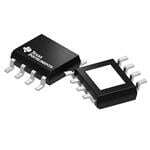
| 描述 | IC DVR HIGH/LOW SIDE 3A 8SOPWR门驱动器 120V Boot,3A Peak,Hi Freq,Hi/Low-Side |
| 产品分类 | PMIC - MOSFET,电桥驱动器 - 外部开关集成电路 - IC |
| 品牌 | Texas Instruments |
| 产品手册 | |
| 产品图片 |
|
| rohs | 符合RoHS无铅 / 符合限制有害物质指令(RoHS)规范要求 |
| 产品系列 | 电源管理 IC,门驱动器,Texas Instruments UCC27201ADDAR- |
| 数据手册 | |
| 产品型号 | UCC27201ADDAR |
| 上升时间 | 8 ns |
| 下降时间 | 7 ns |
| 产品 | MOSFET Gate Drivers |
| 产品种类 | 门驱动器 |
| 供应商器件封装 | 8-SO PowerPad |
| 其它名称 | 296-28428-1 |
| 包装 | 剪切带 (CT) |
| 商标 | Texas Instruments |
| 安装类型 | 表面贴装 |
| 安装风格 | SMD/SMT |
| 封装 | Reel |
| 封装/外壳 | 8-SOIC(0.154",3.90mm 宽)裸焊盘 |
| 封装/箱体 | HSOP-8 |
| 工作温度 | -40°C ~ 140°C |
| 工厂包装数量 | 2500 |
| 延迟时间 | 20ns |
| 最大功率耗散 | 2.7 W |
| 最大工作温度 | + 140 C |
| 最小工作温度 | - 40 C |
| 标准包装 | 1 |
| 激励器数量 | 2 Driver |
| 电压-电源 | 8 V ~ 17 V |
| 电流-峰值 | 3A |
| 电源电压-最大 | 20 V |
| 电源电压-最小 | 8 V |
| 电源电流 | 3.8 mA |
| 类型 | High and Low Side Driver |
| 系列 | UCC27201A |
| 输入类型 | 非反相 |
| 输出数 | 2 |
| 输出电压 | 0.25 V |
| 输出电流 | 3 A |
| 配置 | 高端和低端,独立 |
| 配置数 | 1 |
| 高压侧电压-最大值(自举) | 120V |


- 商务部:美国ITC正式对集成电路等产品启动337调查
- 曝三星4nm工艺存在良率问题 高通将骁龙8 Gen1或转产台积电
- 太阳诱电将投资9.5亿元在常州建新厂生产MLCC 预计2023年完工
- 英特尔发布欧洲新工厂建设计划 深化IDM 2.0 战略
- 台积电先进制程称霸业界 有大客户加持明年业绩稳了
- 达到5530亿美元!SIA预计今年全球半导体销售额将创下新高
- 英特尔拟将自动驾驶子公司Mobileye上市 估值或超500亿美元
- 三星加码芯片和SET,合并消费电子和移动部门,撤换高东真等 CEO
- 三星电子宣布重大人事变动 还合并消费电子和移动部门
- 海关总署:前11个月进口集成电路产品价值2.52万亿元 增长14.8%


PDF Datasheet 数据手册内容提取
Product Sample & Technical Tools & Support & Folder Buy Documents Software Community UCC27200A,UCC27201A SLUSAF9B–FEBRUARY2011–REVISEDJULY2015 UCC2720xA 120-V Boot, 3-A Peak, High-Frequency, High-Side and Low-Side Driver 1 Features 3 Description • DrivesTwoN-ChannelMOSFETsinHigh-Side The UCC2720xA family of high-frequency N-channel 1 MOSFETdriversincludea120-Vbootstrapdiodeand andLow-SideConfiguration high-side/low-side driver with independent inputs for • NegativeVoltageHandlingonHS(–18V) maximum control flexibility. This allows for N-channel • MaximumBootVoltage120V MOSFET control in half-bridge, full-bridge, two-switch • MaximumVDDVoltage20V forward and active clamp forward converters. The low-side and the high-side gate drivers are • On-Chip0.65-VVF,0.6-Ω RDBootstrapDiode independently controlled and matched to 1-ns • Greaterthan1MHzofOperation between the turn-on and turn-off of each other. The • 20-nsPropagationDelayTimes UCC2720xA are based on the popular UCC27200/1 drivers, but offer some enhancements. In order to • 3-ASink,3-ASourceOutputCurrents improve performance in noisy power supply • 8-nsRise/7-nsFallTimewith1000-pFLoad environments the UCC2720xA has an enhanced ESD • 1-nsDelayMatching input structure and also has the ability to withstand a • UndervoltageLockoutforHigh-SideandLow-Side maximumof–18VonitsHSpin. Driver An on-chip bootstrap diode eliminates the external • Offeredin8-PinSOIC(D),PowerPAD™SOIC-8 discrete diodes. Under-voltage lockout is provided for (DDA),SON-8(DRM),SON-9(DRC)andSON-10 both the high-side and the low-side drivers forcing the outputs low if the drive voltage is below the specified (DPR)Packages threshold. • Specifiedfrom–40°Cto140°C Two versions of the UCC27200A are offered. The 2 Applications UCC27200A has high-noise immune CMOS input thresholdswhiletheUCC27201AhasTTL-compatible • PowerSuppliesforTelecom,Datacom,and thresholds. MerchantMarkets Both devices are offered in an 8-pin SOIC (D), • Half-BridgeApplicationsandFull-Bridge PowerPad SOIC-8 (DDA), SON-8 (DRM) package, a Converters 9-pin SON-9 (DRC) package and a 10-pin SON-10 • IsolatedBusArchitecture (DPR)package. • Two-SwitchForwardConverters DeviceInformation(1) • Active-ClampForwardConverters PARTNUMBER PACKAGE BODYSIZE(NOM) • High-VoltageSynchronous-BuckConverters SOIC(8) 4.90mm×3.91mm • Class-DAudioAmplifiers UCC27200A, HSOP(8) 4.89mm×3.90mm SimplifiedApplicationDiagram UCC27201A VSON(9) 3.00mm×3.00mm VSON(8) 4.00mm×4.00mm +12V +100V UCC27201A WSON(10) 4.00mm×4.00mm (1) For all available packages, see the orderable addendum at VDD SECSOINDDEARY theendofthedatasheet. HB CIRCUIT CONPTRWOMLLER HI NTROL DRHIVIE HHOS LI CO DRIVE LO LO UCC27200A/1A VSS ISOLATION AND FEEDBACK 1 An IMPORTANT NOTICE at the end of this data sheet addresses availability, warranty, changes, use in safety-critical applications, intellectualpropertymattersandotherimportantdisclaimers.PRODUCTIONDATA.
UCC27200A,UCC27201A SLUSAF9B–FEBRUARY2011–REVISEDJULY2015 www.ti.com Table of Contents 1 Features.................................................................. 1 7.4 DeviceFunctionalModes........................................13 2 Applications........................................................... 1 8 ApplicationandImplementation........................ 14 3 Description............................................................. 1 8.1 ApplicationInformation............................................14 4 RevisionHistory..................................................... 2 8.2 TypicalApplication .................................................14 5 PinConfigurationandFunctions......................... 3 9 PowerSupplyRecommendations...................... 20 6 Specifications......................................................... 5 10 Layout................................................................... 20 6.1 AbsoluteMaximumRatings......................................5 10.1 LayoutGuidelines.................................................20 6.2 ESDRatings..............................................................5 10.2 LayoutExample....................................................21 6.3 RecommendedOperatingConditions.......................5 11 DeviceandDocumentationSupport................. 22 6.4 ThermalInformation..................................................6 11.1 DocumentationSupport........................................22 6.5 ElectricalCharacteristics...........................................6 11.2 RelatedLinks........................................................22 6.6 TypicalCharacteristics..............................................8 11.3 CommunityResources..........................................22 7 DetailedDescription............................................ 12 11.4 Trademarks...........................................................22 7.1 Overview.................................................................12 11.5 ElectrostaticDischargeCaution............................22 7.2 FunctionalBlockDiagram.......................................12 11.6 Glossary................................................................22 7.3 FeatureDescription.................................................12 12 Mechanical,Packaging,andOrderable Information........................................................... 22 4 Revision History NOTE:Pagenumbersforpreviousrevisionsmaydifferfrompagenumbersinthecurrentversion. ChangesfromRevisionA(July2011)toRevisionB Page • AddedNegativeVoltageHandlingonHS(–18V)toFeaturesList ...................................................................................... 1 • AddedPinConfigurationandFunctionssection,ESDRatingstable,FeatureDescriptionsection,DeviceFunctional Modes,ApplicationandImplementationsection,PowerSupplyRecommendationssection,Layoutsection,Device andDocumentationSupportsection,andMechanical,Packaging,andOrderableInformationsection .............................. 1 ChangesfromOriginal(February2011)toRevisionA Page • AddedSON-10(DPR)PackagetotheListofFEATURES.................................................................................................... 1 • AddedSON-10(DPR)PackagetotheDESCRIPTION......................................................................................................... 1 • ChangedthePINFUNCTIONStable..................................................................................................................................... 4 • AddedAdditionalPINFUNCTIONSinformation..................................................................................................................... 4 • AddedorderinginformationfortheSON-10(DPR)................................................................................................................ 5 • Addednote,"DPR(SON-10)packagecomeseitherinasmallreelof250piecesaspartnumberUCC27200ADPRT, orlargereelspiecesaspartnumberUCC27200ADPRR.".................................................................................................... 5 • AddedtheSON-10packagetotheORDERINGINFORMATIONtable................................................................................. 5 • AddedtheSON-10packagetotheTHERMALINFORMATIONtable................................................................................... 5 • Changedthe"Minimuminputpulsewidth"valueFrom:50nsMaxTo:50nsTyp................................................................ 7 2 SubmitDocumentationFeedback Copyright©2011–2015,TexasInstrumentsIncorporated ProductFolderLinks:UCC27200A UCC27201A
UCC27200A,UCC27201A www.ti.com SLUSAF9B–FEBRUARY2011–REVISEDJULY2015 5 Pin Configuration and Functions DPackage 8-PinSOIC DDAPackage TopView 8-PinSOICWithExposedPowerPAD TopView VDD 1 8 LO VDD 1 8 LO Exposed HB 2 7 VSS HB 2 Thermal 7 VSS Die Pad HO 3 6 LI HO 3 6 LI HS 4 5 HI HS 4 5 HI DRMPackage 8-PinSON DRCPackage TopView 9-PinSON TopView VDD 1 8 LO VDD 1 9 LO Exposed HB 2 Thermal 7 VSS Exposed 8 VSS Die Pad* Thermal HB 2 Die Pad* 7 LI HO 3 6 LI HO 3 6 HI HS 4 5 HI HS 4 5 N/C DPRPackage 10-PinSON TopView VDD 1 10 LO HB 2 9 VSS Exposed Thermal HO 3 8 LI Die Pad HS 4 7 HI NC 5 6 NC Copyright©2011–2015,TexasInstrumentsIncorporated SubmitDocumentationFeedback 3 ProductFolderLinks:UCC27200A UCC27201A
UCC27200A,UCC27201A SLUSAF9B–FEBRUARY2011–REVISEDJULY2015 www.ti.com PinFunctions PIN I/O DESCRIPTION NAME DRM/D/DDA DRC DPR Positivesupplytothelowergatedriver.De-couplethispinto VDD 1 1 1 I VSS(GND).Typicaldecouplingcapacitorrangeis0.22μFto 1.0μF. High-sidebootstrapsupply.Thebootstrapdiodeison-chipbut theexternalbootstrapcapacitorisrequired.Connectpositive HB 2 2 2 I sideofthebootstrapcapacitortothispin.TypicalrangeofHB bypasscapacitoris0.022μFto0.1μF,thevalueisdependant onthegatechargeofthehigh-sideMOSFEThowever. High-sideoutput.Connecttothegateofthehigh-sidepower HO 3 3 3 O MOSFET. High-sidesourceconnection.Connecttosourceofhigh-side HS 4 4 4 I powerMOSFET.Connectnegativesideofbootstrapcapacitorto thispin. HI 5 6 7 I High-sideinput. LI 6 7 8 I Low-sideinput. Negativesupplyterminalforthedevicewhichisgenerally VSS 7 8 9 O grounded. Low-sideoutput.Connecttothegateofthelow-sidepower LO 8 9 10 O MOSFET. N/C — 5 5/6 — Noconnection.PinslabeledN/Chavenoconnection. PowerPAD(1) — — — — ConnecttoalargethermalmasstraceorGNDplaneto dramaticallyimprovethermalperformance. (1) PinVSSandtheexposedthermaldiepadareinternallyconnectedontheDDAandDRMpackagesonly.ElectricallyreferencedtoVSS (GND). 4 SubmitDocumentationFeedback Copyright©2011–2015,TexasInstrumentsIncorporated ProductFolderLinks:UCC27200A UCC27201A
UCC27200A,UCC27201A www.ti.com SLUSAF9B–FEBRUARY2011–REVISEDJULY2015 6 Specifications 6.1 Absolute Maximum Ratings Overoperatingfree-airtemperature,unlessnoted,allvoltagesarewithrespecttoV (1) SS MIN MAX UNIT Supplyvoltagerange, (2)V –0.3 20 V DD InputvoltagesonLIandHI,V ,V –0.3 20 V LI HI DC –0.3 V +0.3 DD OutputvoltageonLO,V V LO Repetitivepulse<100ns(3) –2 V +0.3 DD DC V –0.3 V +0.3 HS HB OutputvoltageonHO,VHO Repetitivepulse<100ns(3) V –2 (VVHB+-0V.3, V HS HB HS <20) DC –1 120 VoltageonHS,V V HS Repetitivepulse<100ns(3) –18 120 VoltageonHB,V –0.3 120 V HB VoltageOnHB-HS –0.3 120 V Operatingvirtualjunctiontemperaturerange,T –40 150 °C J Leadtemperature(soldering,10sec.) 300 °C PowerdissipationatT =25°C(Dpackage) (4) 1.3 W A PowerdissipationatT =25°C(DDApackage) (4) 2.7 W A PowerdissipationatT =25°C(DRMpackage) (4) 3.3 W A PowerdissipationatT =25°C(DRCpackage) (4) 2.86 W A Storagetemperature,T –65 150 °C stg (1) StressesbeyondthoselistedunderAbsoluteMaximumRatingsmaycausepermanentdamagetothedevice.Thesearestressratings only,whichdonotimplyfunctionaloperationofthedeviceattheseoranyotherconditionsbeyondthoseindicatedunderRecommended OperatingConditions.Exposuretoabsolute-maximum-ratedconditionsforextendedperiodsmayaffectdevicereliability. (2) AllvoltagesarewithrespecttoV .Currentsarepositiveinto,negativeoutofthespecifiedterminal. ss (3) Valuesareverifiedbycharacterizationandarenotproductiontested. (4) ThisdatawastakenusingtheJEDECproposedhigh-KtestPCB.SeetheTHERMALCHARACTERISTICSsectionfordetails. 6.2 ESD Ratings VALUE UNIT Humanbodymodel(HBM),perANSI/ESDA/JEDECJS-001(1) 2000 V Electrostaticdischarge V (ESD) Charged-devicemodel(CDM),perJEDECspecificationJESD22-C101(2) 1000 (1) JEDECdocumentJEP155statesthat500-VHBMallowssafemanufacturingwithastandardESDcontrolprocess. (2) JEDECdocumentJEP157statesthat250-VCDMallowssafemanufacturingwithastandardESDcontrolprocess. 6.3 Recommended Operating Conditions overoperatingfree-airtemperaturerange(unlessotherwisenoted) PARAMETER MIN NOM MAX UNIT V Supplyvoltage 8 12 17 V DD V VoltageonHS –1 105 V HS VoltageonHS,(repetitivepulse<100ns) –15 110 V V V +8, V +17, HB VoltageonHB HS HS V V –1 115 DD VoltageslewrateonHS 50 V/ns T Operatingjunctiontemperaturerange –40 140 °C J Copyright©2011–2015,TexasInstrumentsIncorporated SubmitDocumentationFeedback 5 ProductFolderLinks:UCC27200A UCC27201A
UCC27200A,UCC27201A SLUSAF9B–FEBRUARY2011–REVISEDJULY2015 www.ti.com 6.4 Thermal Information UCC27200A UCC27200A UCC27200A UCC27200A UCC27200A /UCC27201A /UCC27201A /UCC27201A /UCC27201A /UCC27201A THERMALMETRIC(1) UNIT DRM(VSON) DRC(VSON) DPR(WSON) D(SOIC) DDA(HSOP) 8PINS 9PINS 10PINS 8PINS 8PINS R Junction-to-ambientthermalresistance 36.2 43.7 34.8 106.5 40.5 °C/W θJA R Junction-to-case(top)thermal θJC(top) 41.6 49.9 32.1 52.9 49 °C/W resistance R Junction-to-boardthermalresistance 13.2 19.1 11.9 46.6 10.2 °C/W θJB ψ Junction-to-topcharacterization JT 0.6 0.6 0.2 9.6 3.1 °C/W parameter ψ Junction-to-boardcharacterization JB 13.4 19.3 12.2 46.1 9.7 °C/W parameter R Junction-to-case(bottom)thermal θJC(bot) 3.1 3.8 1.3 — 1.5 °C/W resistance (1) Formoreinformationabouttraditionalandnewthermalmetrics,seetheSemiconductorandICPackageThermalMetricsapplication report,SPRA953. 6.5 Electrical Characteristics overoperatingfree-airtemperaturerange,V =V =12V,V =V =0V,NoloadonLOorHO,T =T =–40°Cto DD HB HS SS A J +140°C,(unlessotherwisenoted) PARAMETER TESTCONDITIONS MIN TYP MAX UNIT SUPPLYCURRENTS I VDDquiescentcurrent V =V =0 0.4 0.8 mA DD LI HI UCC27200A f=500kHz,C =0 2.5 4 LOAD I VDDoperatingcurrent mA DDO UCC27201A f=500kHz,C =0 3.8 5.5 LOAD I Bootvoltagequiescentcurrent V =V =0V 0.4 0.8 mA HB LI HI I Bootvoltageoperatingcurrent f=500kHz,C =0 2.5 4 mA HBO LOAD I HBtoV quiescentcurrent V =V =110V 0.0005 1 uA HBS SS HS HB I HBtoV operatingcurrent f=500kHz,C =0 0.1 mA HBSO SS LOAD INPUT V Inputrisingthreshold UCC27200A 5.8 8 V HIT V Inputfallingthreshold UCC27200A 3 5.4 V LIT V Inputvoltagehysteresis UCC27200A 0.4 V IHYS V Inputvoltagethreshold UCC27201A 1.7 2.5 V HIT V Inputvoltagethreshold UCC27201A 0.8 1.6 V LIT V InputvoltageHysteresis UCC27201A 100 mV IHYS R Inputpulldownresistance UCC27201A 100 200 350 kΩ IN UNDERVOLTAGEPROTECTION(UVLO) VDDrisingthreshold 6.2 7.1 7.8 V VDDthresholdhysteresis 0.5 V VHBrisingthreshold 5.8 6.7 7.2 V VHBthresholdhysteresis 0.4 V BOOTSTRAPDIODE V Low-currentforwardvoltage I -HB=100μA 0.65 0.85 V F VDD V High-currentforwardvoltage I -HB=100mA 0.85 1.1 V FI VDD I -HB=100mAand80 R Dynamicresistance,ΔVF/ΔI VDD 0.6 1.0 Ω D mA 6 SubmitDocumentationFeedback Copyright©2011–2015,TexasInstrumentsIncorporated ProductFolderLinks:UCC27200A UCC27201A
UCC27200A,UCC27201A www.ti.com SLUSAF9B–FEBRUARY2011–REVISEDJULY2015 Electrical Characteristics (continued) overoperatingfree-airtemperaturerange,V =V =12V,V =V =0V,NoloadonLOorHO,T =T =–40°Cto DD HB HS SS A J +140°C,(unlessotherwisenoted) PARAMETER TESTCONDITIONS MIN TYP MAX UNIT LOGATEDRIVER V Lowleveloutputvoltage I =100mA 0.18 0.4 V LOL LO I =–100mA,V =V - T =-40to125°C LO LOH DD 0.25 0.4 J V LO V Highleveloutputvoltage V LOH I =–100mA,V =V - T =-40to140°C LO LOH DD 0.25 0.42 J V LO Peakpullupcurrent V =0V 3 A LO Peakpulldowncurrent V =12V 3 A LO HOGATEDRIVER V Lowleveloutputvoltage I =100mA 0.18 0.4 V HOL HO I =–100mA,V =V - T =-40to125°C HO HOH HB 0.25 0.4 J V HO V Highleveloutputvoltage V HOH I =–100mA,V =V - T =-40to140°C HO HOH HB 0.25 0.42 J V HO Peakpullupcurrent V =0V 3 A HO Peakpulldowncurrent V =12V 3 A HO PROPAGATIONDELAYS T =-40to125°C C =0 20 45 J LOAD t V fallingtoV falling ns DLFF LI LO T =-40to140°C C =0 20 50 J LOAD T =-40to125°C C =0 20 45 J LOAD t V fallingtoV falling ns DHFF HI HO T =-40to140°C C =0 20 50 J LOAD T =-40to125°C C =0 20 45 J LOAD t V risingtoV rising ns DLRR LI LO T =-40to140°C C =0 20 50 J LOAD T =-40to125°C C =0 20 45 J LOAD t V risingtoV rising ns DHRR HI HO T =-40to140°C C =0 20 50 J LOAD DELAYMATCHING t LION,HIOFF 1 7 ns MON t LIOFF,HION 1 7 ns MOFF OUTPUTRISEANDFALLTIME t LO,HO C =1000pF 8 ns R LOAD t LO,HO C =1000pF 7 ns F LOAD t LO,HO(3Vto9V) C =0.1μF 0.35 0.6 us R LOAD t LO,HO(3Vto9V) C =0.1μF 0.3 0.6 us F LOAD MISCELLANEOUS Minimuminputpulsewidththatchangestheoutput 50 ns Bootstrapdiodeturnofftime I =20mA,I =0.5A(1) (2) 20 ns F REV (1) TypicalvaluesforT =25°C A (2) I :Forwardcurrentappliedtobootstrapdiode,I :Reversecurrentappliedtobootstrapdiode. F REV Copyright©2011–2015,TexasInstrumentsIncorporated SubmitDocumentationFeedback 7 ProductFolderLinks:UCC27200A UCC27201A
UCC27200A,UCC27201A SLUSAF9B–FEBRUARY2011–REVISEDJULY2015 www.ti.com LI Input HI (HI,LI) TDLRR,TDHRR LO Output (HO,LO) TDLFF,TDHFF HO TMON TMOFF Figure1. TimingDiagram 6.6 Typical Characteristics 10.0 10.0 VDD=12V VDD=12V 150oC NoLoadonOutputs NoLoadonOutputs 25oC A A m 150oC m 125oC Current- 125oC Current- Operating 1.0 Operating 1.0 -40oC IDDO- -40oC 25oC IDDO- 0.1 0.1 10 100 1000 10 100 1000 Frequency-kHz Frequency-kHz Figure2.UCC27200AIDDOperatingCurrentvsFrequency Figure3.UCC27201AIDDOperatingCurrentvsFrequency 8 SubmitDocumentationFeedback Copyright©2011–2015,TexasInstrumentsIncorporated ProductFolderLinks:UCC27200A UCC27201A
UCC27200A,UCC27201A www.ti.com SLUSAF9B–FEBRUARY2011–REVISEDJULY2015 Typical Characteristics (continued) 10.0 1.0 HB=12V HB=12V NoLoadonOutputs NoLoadonOutputs mA 150oC mA urrent- 125oC Current- 0.1 150oC C g perating 1.0 Operatin -O 25oC O- 0.01 25oC O S B B H -40oC H I I 125oC -40oC 0.1 0.001 10 100 1000 10 100 1000 Frequency-kHz Frequency-kHz Figure4.BootVoltageOperatingCurrentvsFrequency Figure5.HBtoVSSOperatingCurrentvsFrequency 50 2.0 % T=25oC T=25oC - e g e/VVoltaDD 48 Rising Voltage-V 1.8 Rising oltag 46 hold 1.6 Falling V s hreshold 44 Falling nputThre 1.4 T I put LI- In 42 HI, 1.2 - LI HI, 40 1.0 8 10 12 14 16 18 20 8 10 12 14 16 18 20 VDD-SupplyVoltage-V VDD-SupplyVoltage-V Figure6.UCC27200AInputThresholdvsSupplyVoltage Figure7.UCC27201AInputThresholdvsSupplyVoltage 50 2.0 % VDD=12V VDD=12V - e g olta 48 -V 1.8 V e VDD Rising oltag Rising oltage/ 46 holdV 1.6 hresholdV 44 Falling nputThres 1.4 Falling T I Input 42 HI,LI- 1.2 - LI HI, 40 1.0 -50 -25 0 25 50 75 100 125 150 -50 -25 0 25 50 75 100 125 150 TA-Temperature-oC TA-Temperature-oC Figure8.UCC27200AInputThresholdvsTemperature Figure9.UCC27201AInputThresholdvsTemperature Copyright©2011–2015,TexasInstrumentsIncorporated SubmitDocumentationFeedback 9 ProductFolderLinks:UCC27200A UCC27201A
UCC27200A,UCC27201A SLUSAF9B–FEBRUARY2011–REVISEDJULY2015 www.ti.com Typical Characteristics (continued) 0.45 0.45 0.40 ILO=IHO=-100mA VDD=VHB=16V 0.40 ILO=IHO=100mA V 0.35 VDD=VHB=12V V 0.35 Voltage- 0.30 VDD=VHB=8V Voltage- 0.30 VDD=VHB=1V2DVD=VHB=16V LO/HOOutput 000...122550 LO/HOOutput 000...122550 VDD=VHB=8V VOH- 0.10 VDD=VHB=20V VOL- 0.10 0.05 0.05 VDD=VHB=20V 0.0 0.0 -50 -25 0 25 50 75 100 125 150 -50 -25 0 25 50 75 100 125 150 T -Temperature-oC T -Temperature-oC A A Figure10.LoandHoHighLevelOutputVoltagevs Figure11.LoandHoLowLevelOutputVoltagevs Temperature Temperature 7.8 0.8 7.6 0.7 7.4 0.6 VDDUVLOHysteresis VDDRisingThreshold 7.2 Threshold-V 676...608 Hysteresis-V 000...435 HBUVLOHysteresis 6.4 HBRisingThreshold 0.2 6.2 0.1 6.0 5.8 0 -50 -25 0 25 50 75 100 125 150 -50 -25 0 25 50 75 100 125 150 T -Temperature-oC T -Temperature-oC A A Figure12.UndervoltageLockoutThresholdvsTemperature Figure13.UndervoltageLockoutThresholdHysteresisvs Temperature 36 36 V =V =12V V =V =12V 34 DD HD 34 DD HB TDHFF 32 32 s 30 TDHRR ns 30 elay-n 2268 Delay- 2268 D n Propagation 222204 Propagatio 222204 TDTLDRLRFF 18 TDLFF 18 TDHFF 16 16 TDLRR TDHRR 14 14 -50 -25 0 25 50 75 100 125 150 -50 -25 0 25 50 75 100 125 150 T -Temperature-oC T -Temperature-oC A A Figure14.UCC27200APropagationDelaysvsTemperature Figure15.UCC27201APropagationDelaysvsTemperature 10 SubmitDocumentationFeedback Copyright©2011–2015,TexasInstrumentsIncorporated ProductFolderLinks:UCC27200A UCC27201A
UCC27200A,UCC27201A www.ti.com SLUSAF9B–FEBRUARY2011–REVISEDJULY2015 Typical Characteristics (continued) 26 26 T=25oC T=25oC 24 24 ns ns opagationDelay- 2202 HIFalling LIFallinLgIRising opagationDelay- 22 LIRising LIFalling Pr Pr 20 HIRising 18 HIRising HIFalling 16 18 8 10 12 14 16 18 20 8 10 12 14 16 18 20 V =V -SupplyVoltage-V V =V -SupplyVoltage-V DD HB DD HB Figure16.UCC27200APropagationDelayvsSupplyVoltage Figure17.UCC27201APropagationDelayvsSupplyVoltage 7 3.5 VDD=VHB=12V V =V =12V 6 DD HB 3.0 5 -A 2.5 Pull-UpCurrent Pull-DownCurrent DelayMatching-ns 342 UCC27201ATMUOCNC27200ATUMCOC2FU7FC20C12A7T2M0O0AFTFMON I,I-OutputCurrentLOHO 121...500 1 0.5 0 0 -50 -25 0 25 50 75 100 125 150 0 2 4 6 8 10 12 TA-Temperature-?C VLO,VHO-OutputVoltage-V Figure18.DelayMatchingvsTemperature Figure19.OutputCurrentvsOutputVoltage 100.0 700 InputsLow 600 T=25oC 10.0 A m 500 - mA ent nt- 1.0 Curr 400 IHB DiodeCurre 0.1 I,I-SupplyDDHB 320000 IDD 0.01 100 0.001 0 0.5 0.6 0.7 0.8 0.9 0 4 8 12 16 20 DiodeVoltage-V V ,V -SupplyVoltage-V DD HB Figure20.DiodeCurrentvsDiodeVoltage Figure21.QuiescentCurrentvsSupplyVoltage Copyright©2011–2015,TexasInstrumentsIncorporated SubmitDocumentationFeedback 11 ProductFolderLinks:UCC27200A UCC27201A
UCC27200A,UCC27201A SLUSAF9B–FEBRUARY2011–REVISEDJULY2015 www.ti.com 7 Detailed Description 7.1 Overview The UCC27200A and UCC27201A are high-side and low-side drivers. The high-side and low-side each have independent inputs which allow maximum flexibility of input control signals in the application. The boot diode for the high-side driver bias supply is internal to the UCC27200A and UCC27201A. The UCC27200A is the CMOS compatible input version and the UCC27201A is the TTL or logic compatible version. The high-side driver is referenced to the switch node (HS) which is typically the source pin of the high side MOSFET and drain pin of the low-side MOSFET. The low-side driver is referenced to VSS which is typically ground. The functions containedaretheinputstages,UVLOprotection,levelshift,bootdiode,andoutputdriverstages. 7.2 Functional Block Diagram 2 HB UVLO LEVEL 3 HO SHIFT 4 HS HI 5 V 1 DD UVLO 8 LO LI 6 7 V SS 7.3 Feature Description 7.3.1 InputStages The input stages provide the interface to the PWM output signals. The input impedance of the UCC27200A is 200 kΩ nominal and input capacitance is approximately 2 pF. The 200 kΩ is a pulldown resistance to Vss (ground). The CMOS-compatible input of the UCC27200A provides a rising threshold of 48% of VDD and falling thresholdof45%ofVDD.TheinputsoftheUCC27200Aareintendedtobedrivenfrom0toVDDlevels. The input stages of the UCC27201A incorporate an open-drain configuration to provide the lower input thresholds. The input impedance is 200 kΩ nominal and input capacitance is approximately 4 pF. The 200 kΩ is a pulldown resistance to VSS (ground). The logic level compatible input provides a rising threshold of 1.7 V and afallingthresholdof1.6V. 7.3.1.1 UVLO(UndervoltageLockout) The bias supplies for the high-side and low-side drivers have UVLO protection. VDD as well as VHB to VHS differential voltages are monitored. The VDD UVLO disables both drivers when VDD is below the specified threshold. The rising VDD threshold is 7.1 V with 0.5-V hysteresis. The VHB UVLO disables only the high-side driver when the VHB to VHS differential voltage is below the specified threshold. The VHB UVLO rising threshold is6.7Vwith0.4-Vhysteresis. 12 SubmitDocumentationFeedback Copyright©2011–2015,TexasInstrumentsIncorporated ProductFolderLinks:UCC27200A UCC27201A
UCC27200A,UCC27201A www.ti.com SLUSAF9B–FEBRUARY2011–REVISEDJULY2015 Feature Description (continued) 7.3.1.2 LevelShift The level shift circuit is the interface from the high-side input to the high-side driver stage which is referenced to the switch node (HS). The level shift allows control of the HO output referenced to the HS pin and provides excellentdelaymatchingwiththelow-sidedriver. 7.3.1.3 BootDiode The boot diode necessary to generate the high-side bias is included in the UCC2720x family of drivers. The diode anode is connected to VDD and cathode connected to VHB. With the VHB capacitor connected to HB and the HS pins, the VHB capacitor charge is refreshed every switching cycle when HS transitions to ground. The boot diode provides fast recovery times, low diode resistance, and voltage rating margin to allow for efficient and reliableoperation. 7.3.1.4 OutputStages The output stages are the interface to the power MOSFETs in the power train. High slew rate, low resistance, and high peak current capability of both output drivers allow for efficient switching of the power MOSFETs. The low-sideoutputstageisreferencedfromVDDtoVSSandthehigh-sideisreferencedfromVHBtoVHS. 7.4 Device Functional Modes The device operates in normal mode and VULO mode. See UVLO (Undervoltage Lockout) for more information onUVLOoperationmode.Innormalmode,theoutputstageisdependentonthesatesoftheHIandLIpins. Table1.DeviceLogicTable HIPIN LIPIN HO(1) LO(2) L L L L L H L H H L H L H H H H (1) HOismeasuredwithrespecttotheHS. (2) LOismeasuredwithrespecttotheVSS. Copyright©2011–2015,TexasInstrumentsIncorporated SubmitDocumentationFeedback 13 ProductFolderLinks:UCC27200A UCC27201A
UCC27200A,UCC27201A SLUSAF9B–FEBRUARY2011–REVISEDJULY2015 www.ti.com 8 Application and Implementation NOTE Information in the following applications sections is not part of the TI component specification, and TI does not warrant its accuracy or completeness. TI’s customers are responsible for determining suitability of components for their purposes. Customers should validateandtesttheirdesignimplementationtoconfirmsystemfunctionality. 8.1 Application Information Toeffectfastswitchingofpowerdevicesandreduceassociatedswitchingpowerlosses,apowerfulgatedriveris employed between the PWM output of controllers and the gates of the power semiconductor devices. Also, gate drivers are indispensable when it is impossible for the PWM controller to directly drive the gates of the switching devices. With the advent of digital power, this situation will be often encountered because the PWM signal from the digital controller is often a 3.3-V logic signal which cannot effectively turn on a power switch. Level shifting circuitry is needed to boost the 3.3-V signal to the gate-drive voltage (such as 12 V) in order to fully turn on the power device and minimize conduction losses. Traditional buffer drive circuits based on NPN/PNP bipolar transistors in totem-pole arrangement, being emitter follower configurations, prove inadequate with digital power becausetheylacklevel-shiftingcapability.Gatedriverseffectivelycombineboththelevel-shiftingandbuffer-drive functions. Gate drivers also find other needs such as minimizing the effect of high-frequency switching noise by locating the high-current driver physically close to the power switch, driving gate-drive transformers and controlling floating power-device gates, reducing power dissipation and thermal stress in controllers by moving gatechargepowerlossesfromthecontrollerintothedriver. 8.2 Typical Application Anopenloophalf-bridgeconverterwasusedtocalculateperformanceinanactualapplication. + + + Figure22. OpenLoopHalf-BridgeConverter 14 SubmitDocumentationFeedback Copyright©2011–2015,TexasInstrumentsIncorporated ProductFolderLinks:UCC27200A UCC27201A
UCC27200A,UCC27201A www.ti.com SLUSAF9B–FEBRUARY2011–REVISEDJULY2015 Typical Application (continued) 8.2.1 DesignRequirements UCC27201ADesignRequirements DESIGNPARAMETER EXAMPLEVALUE SupplyVoltage,VDD 12V VoltageonHS,VHS 0Vto100V VoltageonHB,VHB 12Vto112V Output 4V,20A Frequency 200kHz 8.2.2 DetailedDesignProcedure 8.2.2.1 SwitchingtheMOSFETs Achieving optimum drive performance at high frequency efficiently requires special attention to layout and minimizing parasitic inductances. Take care at the driver die and package level as well as the PCB layout to reduce parasitic inductances as much as possible. Figure 23 shows the main parasitic inductance elements and current flow paths during the turnon and turnoff of the MOSFET by charging and discharging its CGS capacitance. L bond wire L trace L pin 1 VDD I SOURCE Cvdd Rsource L trace Driver L bond wire L pin Rg Output 8 Stage LO I sink Rsink Cgs L bond wire L pin L trace L trace 7 Vss Figure23. MOSFETDrivePathsandCircuitParasitics Copyright©2011–2015,TexasInstrumentsIncorporated SubmitDocumentationFeedback 15 ProductFolderLinks:UCC27200A UCC27201A
UCC27200A,UCC27201A SLUSAF9B–FEBRUARY2011–REVISEDJULY2015 www.ti.com The I current charges the C gate capacitor and the I current discharges it. The rise and fall time of SOURCE GS SINK the voltage across the gate to source defines how quickly the MOSFET can be switched. Based on actual measurements, the analytical curves in Figure 24 and Figure 25 indicate the output voltage and current of the drivers during the discharge of the load capacitor. Figure 24 shows voltage and current as a function of time. Figure 25 indicates the relationship of voltage and current during fast switching. These figures demonstrate the actualswitchingprocessandlimitationsduetoparasiticinductances. 12 12 11 11 10 10 9 8 9 7 8 6 7 A 5 OFalling,Vor 234 Voltage,V 456 L 1 LO 3 0 1 2 2 1 3 0 4 1 5 0 2 4 6 8 10 12 14 16 18 20 22 24 26 28 30 2 t,ns 3 2 1 0 1 2 3 4 5 VVoollttaaggee CCuurrrreenntt LOCurrent,A Figure24.TurnoffVoltageandCurrentvsTime Figure25.TurnoffVoltageandCurrentSwitchingDiagram Turning off the MOSFET needs to be achieved as fast as possible to minimize switching losses. For this reason the UCC2720x drivers are designed for high peak currents and low output resistance. The sink capability is specified as 0.18 V at 100-mA dc current implying 1.8-Ω R . With 12-V drive voltage, no parasitic inductance DS(on) and a linear resistance, one would expect initial sink current amplitude of 6.7 A for both high-side and low-side drivers. Assuming a pure R-C discharge circuit of the gate capacitor, one would expect the voltage and current waveforms to be exponential. Due to the parasitic inductances and non-linear resistance of the driver MOSFET’S, the actual waveforms have some ringing and the peak-sink current of the drivers is approximately 3.3 A as shown in Figure 19. The overall parasitic inductance of the drive circuit is estimated at 4 nH. The internal parasitic inductance of the SOIC-8 package is estimated to be 2 nH including bond wires and leads. The SON-8packagereducestheinternalparasiticinductancesbymorethan50%. 16 SubmitDocumentationFeedback Copyright©2011–2015,TexasInstrumentsIncorporated ProductFolderLinks:UCC27200A UCC27201A
UCC27200A,UCC27201A www.ti.com SLUSAF9B–FEBRUARY2011–REVISEDJULY2015 Actual measured waveforms are shown in Figure 26 and Figure 27. As shown, the typical rise time of 8 ns and falltimeof7nsisconservativelyrated. UCC27200A UCC27200A Figure26.V andV RiseTime,1-nfLoad,5ns/div Figure27.V andV FallTime,1-nfLoad,5-ns/div LO HO LO HO 8.2.2.2 DynamicSwitchingoftheMOSFETs The true behavior of MOSFETS presents a dynamic capacitive load primarily at the gate to source threshold voltage. Using the turnoff case as the example, when the gate to source threshold voltage is reached the drain voltage starts rising, the drain to gate parasitic capacitance couples charge into the gate resulting in the turn off plateau. The relatively low threshold voltages of many MOSFETS and the increased charge that has to be removed (Miller charge) makes good driver performance necessary for efficient switching. An open-loop, half- bridge power converter was utilized to evaluate performance in actual applications. The schematic of the half- bridge converter is shown in . The turn off waveforms of the UCC27200A driving two MOSFETs in parallel is showninFigure28andFigure29. UCC27200A UCC27200A Figure29.V FallTimeinHalf-BridgeConverter Figure28.V FallTimeinHalf-BridgeConverter HO LO Copyright©2011–2015,TexasInstrumentsIncorporated SubmitDocumentationFeedback 17 ProductFolderLinks:UCC27200A UCC27201A
UCC27200A,UCC27201A SLUSAF9B–FEBRUARY2011–REVISEDJULY2015 www.ti.com 8.2.2.3 DelayMatchingandNarrowPulseWidths The total delays encountered in the PWM, driver and power stage need to be considered for a number of reasons, primarily delay in current limit response. Also to be considered are differences in delays between the drivers which can lead to various concerns depending on the topology. The sync-buck topology switching requires careful selection of dead-time between the high- and low-side switches to avoid 1) cross conduction and 2) excessive body diode conduction. Bridge topologies can be affected by a resulting volt-sec imbalance on the transformerifthereisimbalanceinthehighandlowsidepulsewidthsinasteady-statecondition. Narrow pulse width performance is an important consideration when transient and short circuit conditions are encountered. Although there may be relatively long steady state PWM output-driver-MOSFET signals, very narrowpulsesmaybeencounteredin1)softstart,2)largeloadtransients,and3)shortcircuitconditions. The UCC2720x driver family offers excellent performance regarding high and low-side driver delay matching and narrow pulse width performance. The delay matching waveforms are shown in Figure 30 and Figure 31. The UCC2720xdrivernarrowpulseperformanceisshowninFigure32andFigure33. Figure30.V andV RisingEdgeDelayMatching Figure31.V andV FallingEdgeDelayMatching LO HO LO HO Figure32.20-nsInputPulseDelayMatching Figure33.10-nsInputPulseDelayMatching 18 SubmitDocumentationFeedback Copyright©2011–2015,TexasInstrumentsIncorporated ProductFolderLinks:UCC27200A UCC27201A
UCC27200A,UCC27201A www.ti.com SLUSAF9B–FEBRUARY2011–REVISEDJULY2015 8.2.2.4 BootDiodePerformance The UCC2720x family of drivers incorporates the bootstrap diode necessary to generate the high-side bias internally. The characteristics of this diode are important to achieve efficient, reliable operation. The dc characteristics to consider are V and dynamic resistance. A low V and high dynamic resistance results in a F F high forward voltage during charging of the bootstrap capacitor. The UCC2720x has a boot diode rated at 0.65-V V and dynamic resistance of 0.6 Ω for reliable charge transfer to the bootstrap capacitor. The dynamic F characteristics to consider are diode recovery time and stored charge. Diode recovery times that are specified with no conditions can be misleading. Diode recovery times at no forward current (I ) can be noticeably less than F with forward current applied. The UCC2720x boot diode recovery is specified at 20ns at I = 20 mA, I = 0.5 A. F REV At0mAI thereverserecoverytimeis15ns. F Anotherlessobviousconsiderationishowthestoredchargeofthediodeisaffectedbyappliedvoltage.Onevery switching transition when the HS node transitions from low to high, charge is removed from the boot capacitor to charge the capacitance of the reverse biased diode. This is a portion of the driver power losses and reduces the voltage on the HB capacitor. At higher applied voltages, the stored charge of the UCC2720x PN diode is often lessthanacomparableSchottkydiode. 8.2.3 ApplicationCurves UCC27200A UCC27200A Figure35.V FallTimeinHalf-BridgeConverter Figure34.V FallTimeinHalf-BridgeConverter HO LO Copyright©2011–2015,TexasInstrumentsIncorporated SubmitDocumentationFeedback 19 ProductFolderLinks:UCC27200A UCC27201A
UCC27200A,UCC27201A SLUSAF9B–FEBRUARY2011–REVISEDJULY2015 www.ti.com 9 Power Supply Recommendations The bias supply voltage range for which the device is rated to operate is from 8 V to 17 V. The lower end of this range is governed by the internal undervoltage-lockout (UVLO) protection feature on the VDD pin supply circuit blocks. Whenever the driver is in UVLO condition when the VDD pin voltage is below the V(ON) supply start threshold, this feature holds the output low, regardless of the status of the inputs. The upper end of this range is driven by the 20-V absolute maximum voltage rating of the VDD pin of the device (which is a stress rating). Keeping a 3-V margin to allow for transient voltage spikes, the maximum recommended voltage for the VDD pin is17V.TheUVLOprotectionfeaturealsoinvolvesahysteresisfunction.ThismeansthatwhentheVDDpinbias voltage has exceeded the threshold voltage and device begins to operate, and if the voltage drops, then the device continues to deliver normal functionality unless the voltage drop exceeds the hysteresis specification VDD(hys).Therefore, ensuring that, while operating at or near the 8-V range, the voltage ripple on the auxiliary power supply output is smaller than the hysteresis specification of the device is important to avoid triggering device shutdown. During system shutdown, the device operation continues until the VDD pin voltage has dropped below the V(OFF) threshold which must be accounted for while evaluating system shutdown timing design requirements. Likewise, at system startup, the device does not begin operation until the VDD pin voltage has exceeded above the V(ON) threshold. The quiescent current consumed by the internal circuit blocks of the device is supplied through the VDD pin. Although this fact is well known, recognizing that the charge for source currentpulsesdeliveredbytheHOpinisalsosuppliedthroughthesameVDDpinisimportant.Asaresult,every time a current is sourced out of the HO pin a corresponding current pulse is delivered into the device through the VDD pin. Thus ensuring that a local bypass capacitor is provided between the VDD and GND pins and located as close to the device as possible for the purpose of decoupling is important. A low ESR, ceramic surface mount capacitor is a must. TI recommends using a capacitor in the range 0.22 uF to 4.7 uF between VDD and GND. In a similar manner, the current pulses delivered by the LO pin are sourced from the HB pin. Therefore a 0.022-uF to0.1-uFlocaldecouplingcapacitorisrecommendedbetweentheHBandHSpins. 10 Layout 10.1 Layout Guidelines Toimprovetheswitchingcharacteristicsandefficiencyofadesign,thefollowinglayoutrulesshouldbefollowed. • LocatethedriverascloseaspossibletotheMOSFETs. • LocatetheV andV (bootstrap)capacitorsascloseaspossibletothedriver. DD HB • Pay close attention to the GND trace. Use the thermal pad of the DDA and DRM package as GND by connecting it to the VSS pin (GND). The GND trace from the driver goes directly to the source of the MOSFETbutshouldnotbeinthehighcurrentpathoftheMOSFET(S)drainorsourcecurrent. • UsesimilarrulesfortheHSnodeasforGNDforthehighsidedriver. • Use wide traces for LO and HO closely following the associated GND or HS traces. 60 mil to 100 mil width is preferablewherepossible. • Use as least two or more vias if the driver outputs or SW node needs to be routed from one layer to another. For GND the number of vias needs to be a consideration of the thermal pad requirements as well as parasitic inductance. • Avoid L and H (driver input) going close to the HS node or any other high dV/dT traces that can induce I I significantnoiseintotherelativelyhighimpedanceleads. • Keep in mind that a poor layout can cause a significant drop in efficiency versus a good PCB layout and can evenleadtodecreasedreliabilityofthewholesystem. Thesereferencesandlinkstoadditionalinformationmaybefoundatwww.ti.com. 1. AdditionallayoutguidelinesforPCBlandpatternsmaybefoundinApplicationBriefSLUA271 2. AdditionalthermalperformanceguidelinesmaybefoundinApplicationReportsSLMA002 andSLMA004 20 SubmitDocumentationFeedback Copyright©2011–2015,TexasInstrumentsIncorporated ProductFolderLinks:UCC27200A UCC27201A
UCC27200A,UCC27201A www.ti.com SLUSAF9B–FEBRUARY2011–REVISEDJULY2015 10.2 Layout Example Figure36. ExampleComponentPlacement Copyright©2011–2015,TexasInstrumentsIncorporated SubmitDocumentationFeedback 21 ProductFolderLinks:UCC27200A UCC27201A
UCC27200A,UCC27201A SLUSAF9B–FEBRUARY2011–REVISEDJULY2015 www.ti.com 11 Device and Documentation Support 11.1 Documentation Support 11.1.1 RelatedDocumentation Forrelateddocumentationseethefollowing: • QFN/SONPCBAttachment,SLUA271 • PowerPADThermallyEnhancedPackage,SLMA002 • PowerPADMadeEasy,SLMA004 11.2 Related Links The table below lists quick access links. Categories include technical documents, support and community resources,toolsandsoftware,andquickaccesstosampleorbuy. Table2.RelatedLinks TECHNICAL TOOLS& SUPPORT& PARTS PRODUCTFOLDER SAMPLE&BUY DOCUMENTS SOFTWARE COMMUNITY UCC27200A Clickhere Clickhere Clickhere Clickhere Clickhere UCC27201A Clickhere Clickhere Clickhere Clickhere Clickhere 11.3 Community Resources The following links connect to TI community resources. Linked contents are provided "AS IS" by the respective contributors. They do not constitute TI specifications and do not necessarily reflect TI's views; see TI's Terms of Use. TIE2E™OnlineCommunity TI'sEngineer-to-Engineer(E2E)Community.Createdtofostercollaboration amongengineers.Ate2e.ti.com,youcanaskquestions,shareknowledge,exploreideasandhelp solveproblemswithfellowengineers. DesignSupport TI'sDesignSupport QuicklyfindhelpfulE2Eforumsalongwithdesignsupporttoolsand contactinformationfortechnicalsupport. 11.4 Trademarks PowerPAD,E2EaretrademarksofTexasInstruments. Allothertrademarksarethepropertyoftheirrespectiveowners. 11.5 Electrostatic Discharge Caution Thesedeviceshavelimitedbuilt-inESDprotection.Theleadsshouldbeshortedtogetherorthedeviceplacedinconductivefoam duringstorageorhandlingtopreventelectrostaticdamagetotheMOSgates. 11.6 Glossary SLYZ022—TIGlossary. Thisglossarylistsandexplainsterms,acronyms,anddefinitions. 12 Mechanical, Packaging, and Orderable Information The following pages include mechanical, packaging, and orderable information. This information is the most current data available for the designated devices. This data is subject to change without notice and revision of thisdocument.Forbrowser-basedversionsofthisdatasheet,refertotheleft-handnavigation. 22 SubmitDocumentationFeedback Copyright©2011–2015,TexasInstrumentsIncorporated ProductFolderLinks:UCC27200A UCC27201A
PACKAGE OPTION ADDENDUM www.ti.com 26-May-2020 PACKAGING INFORMATION Orderable Device Status Package Type Package Pins Package Eco Plan Lead/Ball Finish MSL Peak Temp Op Temp (°C) Device Marking Samples (1) Drawing Qty (2) (6) (3) (4/5) UCC27200AD ACTIVE SOIC D 8 75 Green (RoHS NIPDAU Level-1-260C-UNLIM -40 to 140 27200A & no Sb/Br) UCC27200ADDA ACTIVE SO PowerPAD DDA 8 75 Green (RoHS NIPDAU | NIPDAUAG Level-1-260C-UNLIM -40 to 140 27200A & no Sb/Br) UCC27200ADDAR ACTIVE SO PowerPAD DDA 8 2500 Green (RoHS NIPDAU | NIPDAUAG Level-1-260C-UNLIM -40 to 140 27200A & no Sb/Br) UCC27200ADR ACTIVE SOIC D 8 2500 Green (RoHS NIPDAU Level-1-260C-UNLIM -40 to 140 27200A & no Sb/Br) UCC27200ADRCR ACTIVE VSON DRC 9 3000 Green (RoHS NIPDAU Level-2-260C-1 YEAR -40 to 140 200A & no Sb/Br) UCC27200ADRCT ACTIVE VSON DRC 9 250 Green (RoHS NIPDAU Level-2-260C-1 YEAR -40 to 140 200A & no Sb/Br) UCC27200ADRMR ACTIVE VSON DRM 8 3000 Green (RoHS NIPDAUAG Level-1-260C-UNLIM -40 to 140 27200A & no Sb/Br) UCC27200ADRMT ACTIVE VSON DRM 8 250 Green (RoHS NIPDAUAG Level-1-260C-UNLIM -40 to 140 27200A & no Sb/Br) UCC27201AD ACTIVE SOIC D 8 75 Green (RoHS NIPDAU Level-1-260C-UNLIM -40 to 140 27201A & no Sb/Br) UCC27201ADDA ACTIVE SO PowerPAD DDA 8 75 Green (RoHS NIPDAU | NIPDAUAG Level-1-260C-UNLIM -40 to 140 27201A & no Sb/Br) UCC27201ADDAR ACTIVE SO PowerPAD DDA 8 2500 Green (RoHS NIPDAU | NIPDAUAG Level-1-260C-UNLIM -40 to 140 27201A & no Sb/Br) UCC27201ADPRR ACTIVE WSON DPR 10 3000 Green (RoHS NIPDAU Level-2-260C-1 YEAR -40 to 140 UCC & no Sb/Br) 27201A UCC27201ADPRT ACTIVE WSON DPR 10 250 Green (RoHS NIPDAU Level-2-260C-1 YEAR -40 to 140 UCC & no Sb/Br) 27201A UCC27201ADR ACTIVE SOIC D 8 2500 Green (RoHS NIPDAU Level-1-260C-UNLIM -40 to 140 27201A & no Sb/Br) UCC27201ADRCR ACTIVE VSON DRC 9 3000 Green (RoHS NIPDAU Level-2-260C-1 YEAR -40 to 140 201A & no Sb/Br) UCC27201ADRCT ACTIVE VSON DRC 9 250 Green (RoHS NIPDAU Level-2-260C-1 YEAR -40 to 140 201A & no Sb/Br) UCC27201ADRMR ACTIVE VSON DRM 8 3000 Green (RoHS Call TI | NIPDAUAG Level-1-260C-UNLIM -40 to 140 27201A & no Sb/Br) | NIPDAU Addendum-Page 1
PACKAGE OPTION ADDENDUM www.ti.com 26-May-2020 Orderable Device Status Package Type Package Pins Package Eco Plan Lead/Ball Finish MSL Peak Temp Op Temp (°C) Device Marking Samples (1) Drawing Qty (2) (6) (3) (4/5) UCC27201ADRMT ACTIVE VSON DRM 8 250 Green (RoHS Call TI | NIPDAUAG Level-1-260C-UNLIM -40 to 140 27201A & no Sb/Br) | NIPDAU (1) The marketing status values are defined as follows: ACTIVE: Product device recommended for new designs. LIFEBUY: TI has announced that the device will be discontinued, and a lifetime-buy period is in effect. NRND: Not recommended for new designs. Device is in production to support existing customers, but TI does not recommend using this part in a new design. PREVIEW: Device has been announced but is not in production. Samples may or may not be available. OBSOLETE: TI has discontinued the production of the device. (2) RoHS: TI defines "RoHS" to mean semiconductor products that are compliant with the current EU RoHS requirements for all 10 RoHS substances, including the requirement that RoHS substance do not exceed 0.1% by weight in homogeneous materials. Where designed to be soldered at high temperatures, "RoHS" products are suitable for use in specified lead-free processes. TI may reference these types of products as "Pb-Free". RoHS Exempt: TI defines "RoHS Exempt" to mean products that contain lead but are compliant with EU RoHS pursuant to a specific EU RoHS exemption. Green: TI defines "Green" to mean the content of Chlorine (Cl) and Bromine (Br) based flame retardants meet JS709B low halogen requirements of <=1000ppm threshold. Antimony trioxide based flame retardants must also meet the <=1000ppm threshold requirement. (3) MSL, Peak Temp. - The Moisture Sensitivity Level rating according to the JEDEC industry standard classifications, and peak solder temperature. (4) There may be additional marking, which relates to the logo, the lot trace code information, or the environmental category on the device. (5) Multiple Device Markings will be inside parentheses. Only one Device Marking contained in parentheses and separated by a "~" will appear on a device. If a line is indented then it is a continuation of the previous line and the two combined represent the entire Device Marking for that device. (6) Lead/Ball Finish - Orderable Devices may have multiple material finish options. Finish options are separated by a vertical ruled line. Lead/Ball Finish values may wrap to two lines if the finish value exceeds the maximum column width. Important Information and Disclaimer:The information provided on this page represents TI's knowledge and belief as of the date that it is provided. TI bases its knowledge and belief on information provided by third parties, and makes no representation or warranty as to the accuracy of such information. Efforts are underway to better integrate information from third parties. TI has taken and continues to take reasonable steps to provide representative and accurate information but may not have conducted destructive testing or chemical analysis on incoming materials and chemicals. TI and TI suppliers consider certain information to be proprietary, and thus CAS numbers and other limited information may not be available for release. In no event shall TI's liability arising out of such information exceed the total purchase price of the TI part(s) at issue in this document sold by TI to Customer on an annual basis. OTHER QUALIFIED VERSIONS OF UCC27201A : •Automotive: UCC27201A-Q1 Addendum-Page 2
PACKAGE OPTION ADDENDUM www.ti.com 26-May-2020 NOTE: Qualified Version Definitions: •Automotive - Q100 devices qualified for high-reliability automotive applications targeting zero defects Addendum-Page 3
PACKAGE MATERIALS INFORMATION www.ti.com 1-May-2020 TAPE AND REEL INFORMATION *Alldimensionsarenominal Device Package Package Pins SPQ Reel Reel A0 B0 K0 P1 W Pin1 Type Drawing Diameter Width (mm) (mm) (mm) (mm) (mm) Quadrant (mm) W1(mm) UCC27200ADDAR SO DDA 8 2500 330.0 12.4 6.4 5.2 2.1 8.0 12.0 Q1 Power PAD UCC27200ADR SOIC D 8 2500 330.0 12.5 6.4 5.2 2.1 8.0 12.0 Q1 UCC27200ADRCR VSON DRC 9 3000 330.0 12.4 3.3 3.3 1.1 8.0 12.0 Q2 UCC27200ADRCT VSON DRC 9 250 180.0 12.4 3.3 3.3 1.1 8.0 12.0 Q2 UCC27200ADRMR VSON DRM 8 3000 330.0 12.4 4.25 4.25 1.15 8.0 12.0 Q2 UCC27200ADRMT VSON DRM 8 250 180.0 12.4 4.25 4.25 1.15 8.0 12.0 Q2 UCC27201ADDAR SO DDA 8 2500 330.0 12.8 6.4 5.2 2.1 8.0 12.0 Q1 Power PAD UCC27201ADPRT WSON DPR 10 250 180.0 12.4 4.25 4.25 1.15 8.0 12.0 Q2 UCC27201ADR SOIC D 8 2500 330.0 12.5 6.4 5.2 2.1 8.0 12.0 Q1 UCC27201ADRCR VSON DRC 9 3000 330.0 12.4 3.3 3.3 1.1 8.0 12.0 Q2 UCC27201ADRCT VSON DRC 9 250 180.0 12.4 3.3 3.3 1.1 8.0 12.0 Q2 UCC27201ADRMR VSON DRM 8 3000 330.0 12.4 4.25 4.25 1.15 8.0 12.0 Q2 UCC27201ADRMT VSON DRM 8 250 180.0 12.4 4.25 4.25 1.15 8.0 12.0 Q2 PackMaterials-Page1
PACKAGE MATERIALS INFORMATION www.ti.com 1-May-2020 *Alldimensionsarenominal Device PackageType PackageDrawing Pins SPQ Length(mm) Width(mm) Height(mm) UCC27200ADDAR SOPowerPAD DDA 8 2500 367.0 367.0 35.0 UCC27200ADR SOIC D 8 2500 340.5 338.1 20.6 UCC27200ADRCR VSON DRC 9 3000 367.0 367.0 35.0 UCC27200ADRCT VSON DRC 9 250 210.0 185.0 35.0 UCC27200ADRMR VSON DRM 8 3000 367.0 367.0 35.0 UCC27200ADRMT VSON DRM 8 250 210.0 185.0 35.0 UCC27201ADDAR SOPowerPAD DDA 8 2500 364.0 364.0 27.0 UCC27201ADPRT WSON DPR 10 250 210.0 185.0 35.0 UCC27201ADR SOIC D 8 2500 340.5 338.1 20.6 UCC27201ADRCR VSON DRC 9 3000 367.0 367.0 35.0 UCC27201ADRCT VSON DRC 9 250 210.0 185.0 35.0 UCC27201ADRMR VSON DRM 8 3000 367.0 367.0 35.0 UCC27201ADRMT VSON DRM 8 250 210.0 185.0 35.0 PackMaterials-Page2
GENERIC PACKAGE VIEW DDA 8 PowerPAD TM SOIC - 1.7 mm max height PLASTIC SMALL OUTLINE Images above are just a representation of the package family, actual package may vary. Refer to the product data sheet for package details. 4202561/G
None
None
None
None
None
None
None
None
None
None
None
PACKAGE OUTLINE D0008A SOIC - 1.75 mm max height SCALE 2.800 SMALL OUTLINE INTEGRATED CIRCUIT C SEATING PLANE .228-.244 TYP [5.80-6.19] .004 [0.1] C A PIN 1 ID AREA 6X .050 [1.27] 8 1 2X .189-.197 [4.81-5.00] .150 NOTE 3 [3.81] 4X (0 -15 ) 4 5 8X .012-.020 B .150-.157 [0.31-0.51] .069 MAX [3.81-3.98] .010 [0.25] C A B [1.75] NOTE 4 .005-.010 TYP [0.13-0.25] 4X (0 -15 ) SEE DETAIL A .010 [0.25] .004-.010 0 - 8 [0.11-0.25] .016-.050 [0.41-1.27] DETAIL A (.041) TYPICAL [1.04] 4214825/C 02/2019 NOTES: 1. Linear dimensions are in inches [millimeters]. Dimensions in parenthesis are for reference only. Controlling dimensions are in inches. Dimensioning and tolerancing per ASME Y14.5M. 2. This drawing is subject to change without notice. 3. This dimension does not include mold flash, protrusions, or gate burrs. Mold flash, protrusions, or gate burrs shall not exceed .006 [0.15] per side. 4. This dimension does not include interlead flash. 5. Reference JEDEC registration MS-012, variation AA. www.ti.com
EXAMPLE BOARD LAYOUT D0008A SOIC - 1.75 mm max height SMALL OUTLINE INTEGRATED CIRCUIT 8X (.061 ) [1.55] SYMM SEE DETAILS 1 8 8X (.024) [0.6] SYMM (R.002 ) TYP [0.05] 5 4 6X (.050 ) [1.27] (.213) [5.4] LAND PATTERN EXAMPLE EXPOSED METAL SHOWN SCALE:8X SOLDER MASK SOLDER MASK METAL OPENING OPENING METAL UNDER SOLDER MASK EXPOSED METAL EXPOSED METAL .0028 MAX .0028 MIN [0.07] [0.07] ALL AROUND ALL AROUND NON SOLDER MASK SOLDER MASK DEFINED DEFINED SOLDER MASK DETAILS 4214825/C 02/2019 NOTES: (continued) 6. Publication IPC-7351 may have alternate designs. 7. Solder mask tolerances between and around signal pads can vary based on board fabrication site. www.ti.com
EXAMPLE STENCIL DESIGN D0008A SOIC - 1.75 mm max height SMALL OUTLINE INTEGRATED CIRCUIT 8X (.061 ) [1.55] SYMM 1 8 8X (.024) [0.6] SYMM (R.002 ) TYP [0.05] 5 4 6X (.050 ) [1.27] (.213) [5.4] SOLDER PASTE EXAMPLE BASED ON .005 INCH [0.125 MM] THICK STENCIL SCALE:8X 4214825/C 02/2019 NOTES: (continued) 8. Laser cutting apertures with trapezoidal walls and rounded corners may offer better paste release. IPC-7525 may have alternate design recommendations. 9. Board assembly site may have different recommendations for stencil design. www.ti.com
None
None
www.ti.com
IMPORTANTNOTICEANDDISCLAIMER TI PROVIDES TECHNICAL AND RELIABILITY DATA (INCLUDING DATASHEETS), DESIGN RESOURCES (INCLUDING REFERENCE DESIGNS), APPLICATION OR OTHER DESIGN ADVICE, WEB TOOLS, SAFETY INFORMATION, AND OTHER RESOURCES “AS IS” AND WITH ALL FAULTS, AND DISCLAIMS ALL WARRANTIES, EXPRESS AND IMPLIED, INCLUDING WITHOUT LIMITATION ANY IMPLIED WARRANTIES OF MERCHANTABILITY, FITNESS FOR A PARTICULAR PURPOSE OR NON-INFRINGEMENT OF THIRD PARTY INTELLECTUAL PROPERTY RIGHTS. These resources are intended for skilled developers designing with TI products. You are solely responsible for (1) selecting the appropriate TI products for your application, (2) designing, validating and testing your application, and (3) ensuring your application meets applicable standards, and any other safety, security, or other requirements. These resources are subject to change without notice. TI grants you permission to use these resources only for development of an application that uses the TI products described in the resource. Other reproduction and display of these resources is prohibited. No license is granted to any other TI intellectual property right or to any third party intellectual property right. TI disclaims responsibility for, and you will fully indemnify TI and its representatives against, any claims, damages, costs, losses, and liabilities arising out of your use of these resources. TI’s products are provided subject to TI’s Terms of Sale (www.ti.com/legal/termsofsale.html) or other applicable terms available either on ti.com or provided in conjunction with such TI products. TI’s provision of these resources does not expand or otherwise alter TI’s applicable warranties or warranty disclaimers for TI products. Mailing Address: Texas Instruments, Post Office Box 655303, Dallas, Texas 75265 Copyright © 2020, Texas Instruments Incorporated