ICGOO在线商城 > 分立半导体产品 > 晶体管 - 双极 (BJT) - 单 > SS8550DTA

 Datasheet下载
- 型号: SS8550DTA
- 制造商: Fairchild Semiconductor
- 库位|库存: xxxx|xxxx
- 要求:
| 数量阶梯 | 香港交货 | 国内含税 |
| +xxxx | $xxxx | ¥xxxx |
查看当月历史价格
查看今年历史价格
SS8550DTA产品简介:
ICGOO电子元器件商城为您提供SS8550DTA由Fairchild Semiconductor设计生产,在icgoo商城现货销售,并且可以通过原厂、代理商等渠道进行代购。 SS8550DTA价格参考¥0.30-¥0.38。Fairchild SemiconductorSS8550DTA封装/规格:晶体管 - 双极 (BJT) - 单, Bipolar (BJT) Transistor PNP 25V 1.5A 200MHz 1W Through Hole TO-92-3。您可以下载SS8550DTA参考资料、Datasheet数据手册功能说明书,资料中有SS8550DTA 详细功能的应用电路图电压和使用方法及教程。
SS8550DTA是ON Semiconductor生产的一款PNP型双极结型晶体管(BJT),常用于低功率放大和开关应用。该器件采用SOT-23小外形封装,体积小巧,适合高密度贴装的电路板设计。

其典型应用场景包括:便携式电子设备中的信号开关与电平转换,如智能手机、平板电脑和可穿戴设备;在电源管理电路中作为负载开关或驱动元件;在LED驱动电路中用于控制小功率LED的通断;还可用于音频放大器的前置放大级或互补输出级,配合NPN晶体管(如SS8050)构成推挽放大电路,提升信号驱动能力。

此外,SS8550DTA也广泛应用于各类消费类电子产品中的脉冲宽度调制(PWM)控制、继电器驱动、传感器信号调理等低压、低电流开关场合。由于其具备良好的增益特性和开关响应速度,且工作稳定、成本低廉,因此在家电控制板、无线模块、充电器控制电路中也十分常见。

总之,SS8550DTA凭借其可靠的性能和紧凑的封装,适用于需要小型化、低功耗和高性价比的通用模拟与数字开关电路。
| 参数 | 数值 |
| 产品目录 | |
| 描述 | TRANSISTOR PNP 25V 1.5A TO-92两极晶体管 - BJT TO92 PNP 2W A/P |
| 产品分类 | 晶体管(BJT) - 单路分离式半导体 |
| 品牌 | Fairchild Semiconductor |
| 产品手册 | |
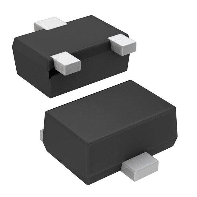
| 产品图片 |
|
| rohs | 符合RoHS无铅 / 符合限制有害物质指令(RoHS)规范要求 |
| 产品系列 | 晶体管,两极晶体管 - BJT,Fairchild Semiconductor SS8550DTA- |
| 数据手册 | |
| 产品型号 | SS8550DTA |
| PCN设计/规格 | |
| 不同 Ib、Ic时的 Vce饱和值(最大值) | 500mV @ 80mA,800mA |
| 不同 Ic、Vce 时的DC电流增益(hFE)(最小值) | 160 @ 100mA,1V |
| 产品种类 | 两极晶体管 - BJT |
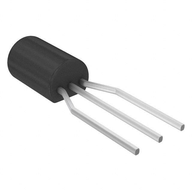
| 供应商器件封装 | TO-92-3 |
| 其它名称 | SS8550DTACT |
| 功率-最大值 | 1W |
| 包装 | 剪切带 (CT) |
| 单位重量 | 240 mg |
| 发射极-基极电压VEBO | - 6 V |
| 商标 | Fairchild Semiconductor |
| 增益带宽产品fT | 200 MHz |
| 安装类型 | 通孔 |
| 安装风格 | Through Hole |
| 封装 | Ammo Pack |
| 封装/外壳 | TO-226-3、TO-92-3(TO-226AA)成形引线 |
| 封装/箱体 | TO-92-3 Kinked Lead |
| 工厂包装数量 | 2000 |
| 晶体管极性 | PNP |
| 晶体管类型 | PNP |
| 最大功率耗散 | 1 W |
| 最大工作温度 | + 150 C |
| 最大直流电集电极电流 | 1.5 A |
| 最小工作温度 | - 65 C |
| 标准包装 | 1 |
| 电压-集射极击穿(最大值) | 25V |
| 电流-集电极(Ic)(最大值) | 1.5A |
| 电流-集电极截止(最大值) | 100nA |
| 直流电流增益hFE最大值 | 300 |
| 直流集电极/BaseGainhfeMin | 85 |
| 系列 | SS8550 |
| 配置 | Single |
| 集电极—发射极最大电压VCEO | - 25 V |
| 集电极—基极电压VCBO | - 40 V |
| 集电极—射极饱和电压 | - 0.28 V |
| 集电极连续电流 | - 1.5 A |
| 频率-跃迁 | 200MHz |

,TO-226_straightlead.jpg)


- 商务部:美国ITC正式对集成电路等产品启动337调查
- 曝三星4nm工艺存在良率问题 高通将骁龙8 Gen1或转产台积电
- 太阳诱电将投资9.5亿元在常州建新厂生产MLCC 预计2023年完工
- 英特尔发布欧洲新工厂建设计划 深化IDM 2.0 战略
- 台积电先进制程称霸业界 有大客户加持明年业绩稳了
- 达到5530亿美元!SIA预计今年全球半导体销售额将创下新高
- 英特尔拟将自动驾驶子公司Mobileye上市 估值或超500亿美元
- 三星加码芯片和SET,合并消费电子和移动部门,撤换高东真等 CEO
- 三星电子宣布重大人事变动 还合并消费电子和移动部门
- 海关总署:前11个月进口集成电路产品价值2.52万亿元 增长14.8%


PDF Datasheet 数据手册内容提取
Is Now Part of To learn more about ON Semiconductor, please visit our website at www.onsemi.com Please note: As part of the Fairchild Semiconductor integration, some of the Fairchild orderable part numbers will need to change in order to meet ON Semiconductor’s system requirements. Since the ON Semiconductor product management systems do not have the ability to manage part nomenclature that utilizes an underscore (_), the underscore (_) in the Fairchild part numbers will be changed to a dash (-). This document may contain device numbers with an underscore (_). Please check the ON Semiconductor website to verify the updated device numbers. The most current and up-to-date ordering information can be found at www.onsemi.com. Please email any questions regarding the system integration to Fairchild_questions@onsemi.com. ON Semiconductor and the ON Semiconductor logo are trademarks of Semiconductor Components Industries, LLC dba ON Semiconductor or its subsidiaries in the United States and/or other countries. ON Semiconductor owns the rights to a number of patents, trademarks, copyrights, trade secrets, and other intellectual property. A listing of ON Semiconductor’s product/patent coverage may be accessed at www.onsemi.com/site/pdf/Patent-Marking.pdf. ON Semiconductor reserves the right to make changes without further notice to any products herein. ON Semiconductor makes no warranty, representation or guarantee regarding the suitability of its products for any particular purpose, nor does ON Semiconductor assume any liability arising out of the application or use of any product or circuit, and specifically disclaims any and all liability, including without limitation special, consequential or incidental damages. Buyer is responsible for its products and applications using ON Semiconductor products, including compliance with all laws, regulations and safety requirements or standards, regardless of any support or applications information provided by ON Semiconductor. “Typical” parameters which may be provided in ON Semiconductor data sheets and/or specifications can and do vary in different applications and actual performance may vary over time. All operating parameters, including “Typicals” must be validated for each customer application by customer’s technical experts. ON Semiconductor does not convey any license under its patent rights nor the rights of others. ON Semiconductor products are not designed, intended, or authorized for use as a critical component in life support systems or any FDA Class 3 medical devices or medical devices with a same or similar classification in a foreign jurisdiction or any devices intended for implantation in the human body. Should Buyer purchase or use ON Semiconductor products for any such unintended or unauthorized application, Buyer shall indemnify and hold ON Semiconductor and its officers, employees, subsidiaries, affiliates, and distributors harmless against all claims, costs, damages, and expenses, and reasonable attorney fees arising out of, directly or indirectly, any claim of personal injury or death associated with such unintended or unauthorized use, even if such claim alleges that ON Semiconductor was negligent regarding the design or manufacture of the part. ON Semiconductor is an Equal Opportunity/Affirmative Action Employer. This literature is subject to all applicable copyright laws and is not for resale in any manner.
S S 8 5 November 2014 5 0 — P N P SS8550 E p PNP Epitaxial Silicon Transistor it a x i a l S i l i Features c o n • 2 W Output Amplifier of Portable Radios in Class B Push-pull Operation. T • Complimentary to SS8050 ra n • Collector Current: IC = 1.5 A s i s t o TO-92 1 r 1. Emitter 2. Base 3. Collector Ordering Information Part Number Top Mark Package Packing Method SS8550BBU S8550 TO-92 3L Bulk SS8550CBU S8550 TO-92 3L Bulk SS8550CTA S8550 TO-92 3L Ammo SS8550DBU S8550 TO-92 3L Bulk SS8550DTA S8550 TO-92 3L Ammo Absolute Maximum Ratings Stresses exceeding the absolute maximum ratings may damage the device. The device may not function or be opera- ble above the recommended operating conditions and stressing the parts to these levels is not recommended. In addi- tion, extended exposure to stresses above the recommended operating conditions may affect device reliability. The absolute maximum ratings are stress ratings only. Values are at T = 25°C unless otherwise noted. A Symbol Parameter Value Unit V Collector-Base Voltage -40 V CBO V Collector-Emitter Voltage -25 V CEO V Emitter-Base Voltage -6 V EBO I Collector Current -1.5 A C T Junction Temperature 150 °C J T Storage Temperature -65 to 150 °C STG © 2002 Fairchild Semiconductor Corporation www.fairchildsemi.com SS8550 Rev. 1.1.0
S S Thermal Characteristics(1) 8 5 5 Values are at TA = 25°C unless otherwise noted. 0 — Symbol Parameter Value Unit P Power Dissipation 1 W N PD Derate Above 25°C 8 mW/°C P E RθJA Thermal Resistance, Junction-to-Ambient 125 °C/W pi t a Note: x i 1. PCB size: FR-4, 76 mm x 114 mm x 1.57 mm (3.0 inch x 4.5 inch x 0.062 inch) with minimum land pattern size. a l S i l i c Electrical Characteristics o n Values are at T = 25°C unless otherwise noted. T A r a Symbol Parameter Conditions Min. Typ. Max. Unit n s BV Collector-Base Breakdown Voltage I = -100 μA, I = 0 -40 V is CBO C E t o BVCEO Collector-Emitter Breakdown Voltage IC = -2 mA, IB = 0 -25 V r BV Emitter-Base Breakdown Voltage I = -100 μA, I = 0 -6 V EBO E C I Collector Cut-Off Current V = -35 V, I = 0 -100 nA CBO CB E I Emitter Cut-Off Current V = -6 V, I = 0 -100 nA EBO EB C h V = -1 V, I = -5 mA 45 170 FE1 CE C h DC Current Gain V = -1 V, I = -100 mA 85 160 300 FE2 CE C h V = -1 V, I = -800 mA 40 80 FE3 CE C V (sat) Collector-Emitter Saturation Voltage I = -800 mA, I = -80 mA -0.28 -0.50 V CE C B V (sat) Base-Emitter Saturation Voltage I = -800 mA, I = -80 mA -0.98 -1.20 V BE C B V (on) Base-Emitter On Voltage V = -1 V, I = -10 mA -0.66 -1.00 V BE CE C V = -10 V, I = 0, C Output Capacitance CB E 15 pF ob f = 1 MHz fT Current Gain Bandwidth Product VCE = -10 V, IC = -50 mA 100 200 MHz h Classification FE Classification B C D h 85 ~ 160 120 ~ 200 160 ~ 300 FE2 © 2002 Fairchild Semiconductor Corporation www.fairchildsemi.com SS8550 Rev. 1.1.0 2
S S Typical Performance Characteristics 8 5 5 0 — P -0.5 1000 N IB=-4.0mA VCE = -1V P R CURRENT --00..34 IIBBIB===--3-32..5.05mmmAAA NT GAIN 100 Epitax mA], COLLECTO --00..12 IIIBBB===---211...050mmmAAA h, DC CURREFE 10 ial Silico I[C IB=-0.5mA n 1 T -0.4 -0.8 -1.2 -1.6 -2.0 -0.1 -1 -10 -100 -1000 r a n VCE[V], COLLECTOR-EMITTER VOLTAGE IC[mA], COLLECTOR CURRENT s i s Figure 1. Static Characteristic Figure 2. DC Current Gain t o r -10000 -100 GE IC=10IB VCE = -1V A T N VOL RENT O -1000 R -10 RATI VBE(sat) R CU U O V(sat)[V], SATCE -100 VCE(sat) mA], COLLECT -1 at), I[C V(sBE -10-0.1 -1 -10 -100 -1000 -0.1-0.0 -0.2 -0.4 -0.6 -0.8 -1.0 -1.2 IC[mA], COLLECTOR CURRENT VBE[V], BASE-EMITTER VOLTAGE Figure 3. Base-Emitter Saturation Voltage and Figure 4. Base-Emitter On Voltage Collector-Emitter Saturation Voltage 100 CT 1000 f=1MHz DU VCE=-10V IE=0 RO P H NCE WIDT CITA AND A 10 B 100 AP N- C AI C[pF], ob RENT G R U C 1 Hz], 10 -1 -10 -100 -1000 M -1 -10 -100 -1000 f[T VCB[V], COLLECTOR-BASE VOLTAGE IC[mA], COLLECTOR CURRENT Figure 5. Collector Output Capacitance Figure 6. Current Gain Bandwidth Product © 2002 Fairchild Semiconductor Corporation www.fairchildsemi.com SS8550 Rev. 1.1.0 3
None
None
ON Semiconductor and are trademarks of Semiconductor Components Industries, LLC dba ON Semiconductor or its subsidiaries in the United States and/or other countries. ON Semiconductor owns the rights to a number of patents, trademarks, copyrights, trade secrets, and other intellectual property. A listing of ON Semiconductor’s product/patent coverage may be accessed at www.onsemi.com/site/pdf/Patent−Marking.pdf. ON Semiconductor reserves the right to make changes without further notice to any products herein. ON Semiconductor makes no warranty, representation or guarantee regarding the suitability of its products for any particular purpose, nor does ON Semiconductor assume any liability arising out of the application or use of any product or circuit, and specifically disclaims any and all liability, including without limitation special, consequential or incidental damages. Buyer is responsible for its products and applications using ON Semiconductor products, including compliance with all laws, regulations and safety requirements or standards, regardless of any support or applications information provided by ON Semiconductor. “Typical” parameters which may be provided in ON Semiconductor data sheets and/or specifications can and do vary in different applications and actual performance may vary over time. All operating parameters, including “Typicals” must be validated for each customer application by customer’s technical experts. ON Semiconductor does not convey any license under its patent rights nor the rights of others. ON Semiconductor products are not designed, intended, or authorized for use as a critical component in life support systems or any FDA Class 3 medical devices or medical devices with a same or similar classification in a foreign jurisdiction or any devices intended for implantation in the human body. Should Buyer purchase or use ON Semiconductor products for any such unintended or unauthorized application, Buyer shall indemnify and hold ON Semiconductor and its officers, employees, subsidiaries, affiliates, and distributors harmless against all claims, costs, damages, and expenses, and reasonable attorney fees arising out of, directly or indirectly, any claim of personal injury or death associated with such unintended or unauthorized use, even if such claim alleges that ON Semiconductor was negligent regarding the design or manufacture of the part. ON Semiconductor is an Equal Opportunity/Affirmative Action Employer. This literature is subject to all applicable copyright laws and is not for resale in any manner. PUBLICATION ORDERING INFORMATION LITERATURE FULFILLMENT: N. American Technical Support: 800−282−9855 Toll Free ON Semiconductor Website: www.onsemi.com Literature Distribution Center for ON Semiconductor USA/Canada 19521 E. 32nd Pkwy, Aurora, Colorado 80011 USA Europe, Middle East and Africa Technical Support: Order Literature: http://www.onsemi.com/orderlit Phone: 303−675−2175 or 800−344−3860 Toll Free USA/Canada Phone: 421 33 790 2910 Fax: 303−675−2176 or 800−344−3867 Toll Free USA/Canada Japan Customer Focus Center For additional information, please contact your local Email: orderlit@onsemi.com Phone: 81−3−5817−1050 Sales Representative © Semiconductor Components Industries, LLC www.onsemi.com www.onsemi.com 1
Mouser Electronics Authorized Distributor Click to View Pricing, Inventory, Delivery & Lifecycle Information: O N Semiconductor: SS8550CBU SS8550BBU SS8550BTA SS8550DBU SS8550CTA SS8550DTA SS8550DTA_Q SS8550CTA_Q