ICGOO在线商城 > 电路保护 > TVS - 混合技术 > SN65240PWR

 Datasheet下载
- 型号: SN65240PWR
- 制造商: Texas Instruments
- 库位|库存: xxxx|xxxx
- 要求:
| 数量阶梯 | 香港交货 | 国内含税 |
| +xxxx | $xxxx | ¥xxxx |
查看当月历史价格
查看今年历史价格
SN65240PWR产品简介:
ICGOO电子元器件商城为您提供SN65240PWR由Texas Instruments设计生产,在icgoo商城现货销售,并且可以通过原厂、代理商等渠道进行代购。 SN65240PWR价格参考¥3.11-¥3.88。Texas InstrumentsSN65240PWR封装/规格:TVS - 混合技术, 。您可以下载SN65240PWR参考资料、Datasheet数据手册功能说明书,资料中有SN65240PWR 详细功能的应用电路图电压和使用方法及教程。
SN65240PWR是德州仪器(Texas Instruments)推出的一款采用混合技术的TVS(瞬态电压抑制)器件,主要用于保护高速数据线路免受静电放电(ESD)、电快速瞬变(EFT)和雷击浪涌等瞬态电压干扰。该器件集成了先进的聚合物与硅基TVS技术,兼具低电容、低钳位电压和高浪涌承受能力的优点,适用于对信号完整性和可靠性要求较高的场景。

典型应用场景包括:工业通信接口(如RS-485、CAN总线)、消费类电子设备的数据端口(如USB、HDMI)、便携式设备以及工厂自动化系统中的信号线路保护。其小尺寸PWP(TSSOP-20)封装适合空间受限的设计,同时支持多通道保护,可有效提升系统抗干扰能力和长期稳定性。SN65240PWR特别适用于恶劣电磁环境下的精密电子设备,确保在瞬态过压事件中维持正常运行,防止敏感元件损坏。
| 参数 | 数值 |
| 产品目录 | |
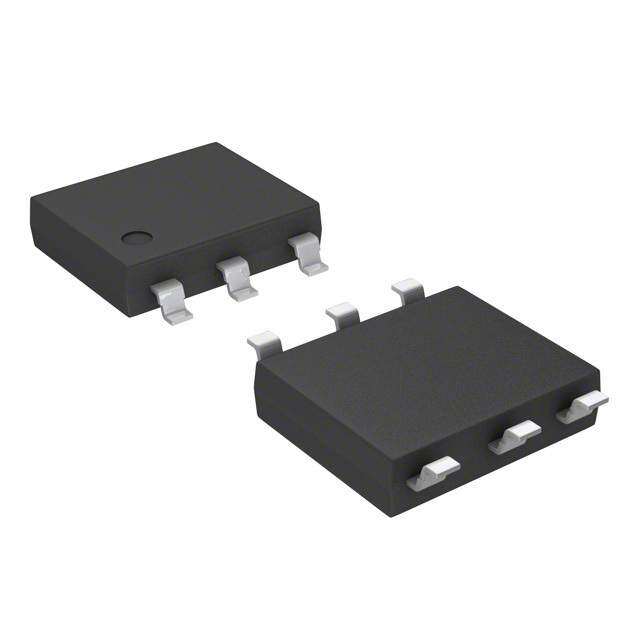
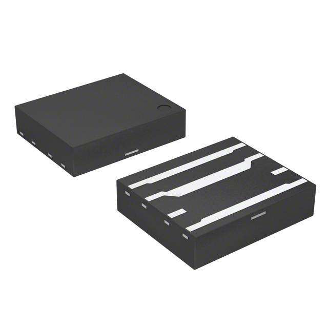
| 描述 | IC DUAL USB PORT TVS 8-TSSOPTVS二极管阵列 Dual USB Port |
| 产品分类 | |
| 品牌 | Texas Instruments |
| 产品手册 | http://www.ti.com/lit/gpn/sn65240 |
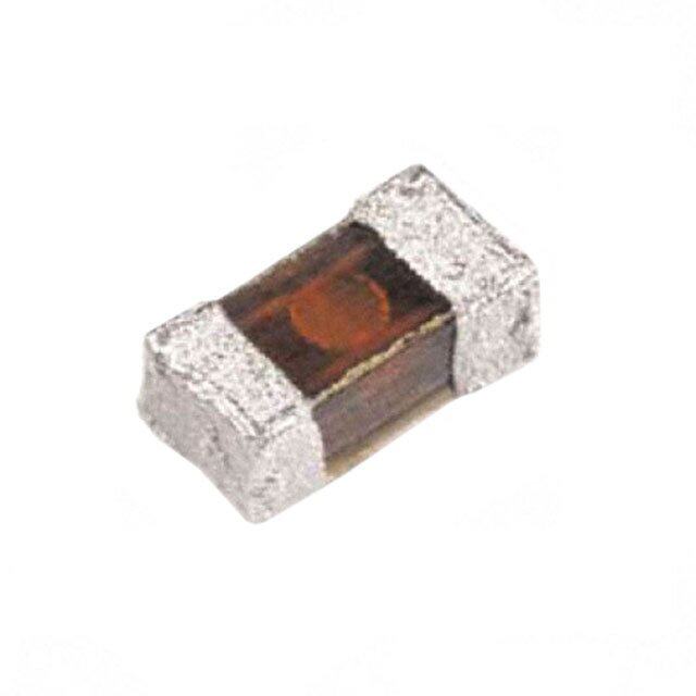
| 产品图片 |
|
| rohs | 符合RoHS无铅 / 符合限制有害物质指令(RoHS)规范要求 |
| 产品系列 | 二极管与整流器,TVS二极管,TVS二极管阵列,Texas Instruments SN65240PWR- |
| 数据手册 | |
| 产品型号 | SN65240PWR |
| 产品目录页面 | |
| 产品种类 | TVS二极管阵列 |
| 供应商器件封装 | 8-TSSOP |
| 其它名称 | 296-9696-1 |
| 击穿电压 | 7 V |
| 制造商产品页 | http://www.ti.com/general/docs/suppproductinfo.tsp?distId=10&orderablePartNumber=SN65240PWR |
| 功率(W) | 60W |
| 包装 | 剪切带 (CT) |
| 单位重量 | 39 mg |
| 商标 | Texas Instruments |
| 外壳高度 | 1.6 mm |
| 安装风格 | SMD/SMT |
| 封装 | Reel |
| 封装/外壳 | 8-TSSOP(0.173",4.40mm 宽) |
| 封装/箱体 | TSSOP-8 |
| 尺寸 | 4.4 mm W x 3 mm L x 1.15 mm H |
| 峰值浪涌电流 | 3 A |
| 峰值脉冲功率耗散 | 60 W |
| 工作电压 | 8 V |
| 工厂包装数量 | 2000 |
| 应用 | USB |
| 技术 | 混合技术 |
| 最大工作温度 | + 85 C |
| 最小工作温度 | - 40 C |
| 极性 | Unidirectional |
| 标准包装 | 1 |
| 电压-工作 | 6V |
| 电压-箝位 | 7V |
| 电容 | 35 pF |
| 电路数 | 1 |
| 端接类型 | SMD/SMT |
| 系列 | SN65240 |
| 通道 | 4 Channels |


- 商务部:美国ITC正式对集成电路等产品启动337调查
- 曝三星4nm工艺存在良率问题 高通将骁龙8 Gen1或转产台积电
- 太阳诱电将投资9.5亿元在常州建新厂生产MLCC 预计2023年完工
- 英特尔发布欧洲新工厂建设计划 深化IDM 2.0 战略
- 台积电先进制程称霸业界 有大客户加持明年业绩稳了
- 达到5530亿美元!SIA预计今年全球半导体销售额将创下新高
- 英特尔拟将自动驾驶子公司Mobileye上市 估值或超500亿美元
- 三星加码芯片和SET,合并消费电子和移动部门,撤换高东真等 CEO
- 三星电子宣布重大人事变动 还合并消费电子和移动部门
- 海关总署:前11个月进口集成电路产品价值2.52万亿元 增长14.8%


PDF Datasheet 数据手册内容提取
Product Sample & Technical Tools & Support & Folder Buy Documents Software Community SN65220,SN65240,SN75240 SLLS266H–FEBRUARY1997–REVISEDMAY2015 SNx52x0 USB Port Transient Suppressors 1 Features 3 Description • DesigntoProtectSubmicron3-Vor5-V The SN65220 device is a dual, and the SN65240 and 1 SN75240 devices are quadruple, unidirectional CircuitsfromNoiseTransients transient voltage suppressors (TVS). These devices • PortESDProtectionCapabilityExceeds: provide electrical noise transient protection to – 15-kVHumanBodyModel Universal Serial Bus (USB) low and full-speed ports. – 2-kVMachineModel The input capacitance of 35 pF makes it unsuitable forhigh-speedUSB2.0applications. • AvailableinaWCSPChip-ScalePackage Any cabled I/O can be subjected to electrical noise • Stand-OffVoltage:6V(Min) transients from various sources. These noise • LowCurrentLeakage:1-µAMaxat6V transients can cause damage to the USB transceiver • LowCapacitance:35-pF(Typ) and/or the USB ASIC if they are of sufficient magnitudeandduration. 2 Applications The ESD performance of the SN65220, SN65240, • USBFull-SpeedHost,HUB,orPeripheral and SN75240 devices is measured at the system level, according to IEC61000-4-2. However, system • Ports design impacts the results of these tests. To accomplish a high compliance level requires careful boarddesignandlayouttechniques. DeviceInformation(1) PARTNUMBER PACKAGE BODYSIZE(NOM) SOT-23(6) 2.90mm×1.60mm SN65220 DSBGA(4) 0.925mm×0.925mm SN65240 PDIP(8) 9.09mm×6.35mm SN75240 TSSOP(8) 3.00mm×4.40mm (1) For all available packages, see the orderable addendum at theendofthedatasheet. TVSCurrentvsVoltage 4 Simplified Schematic 7.5 USB 5 Transceiver A 2.5 – 27O nt 0 D+ e A urr -2.5 C 15kO -5 GND SN65220or ½SNx5240 -7.5 15kO -10 B D- -10 -5 0 5 10 15 27O Voltage–V 1 An IMPORTANT NOTICE at the end of this data sheet addresses availability, warranty, changes, use in safety-critical applications, intellectualpropertymattersandotherimportantdisclaimers.PRODUCTIONDATA.
SN65220,SN65240,SN75240 SLLS266H–FEBRUARY1997–REVISEDMAY2015 www.ti.com Table of Contents 1 Features.................................................................. 1 10.2 FunctionalBlockDiagram.......................................6 2 Applications........................................................... 1 10.3 FeatureDescription.................................................7 3 Description............................................................. 1 10.4 DeviceFunctionalModes........................................7 4 SimplifiedSchematic............................................. 1 11 ApplicationandImplementation.......................... 8 11.1 ApplicationInformation............................................8 5 RevisionHistory..................................................... 2 11.2 TypicalApplication .................................................8 6 DeviceComparisonTable..................................... 3 12 PowerSupplyRecommendations..................... 10 7 PinConfigurationandFunctions......................... 3 13 Layout................................................................... 10 8 Specifications......................................................... 4 13.1 LayoutGuidelines.................................................10 8.1 AbsoluteMaximumRatings......................................4 13.2 LayoutExample....................................................10 8.2 ESDRatings..............................................................4 14 DeviceandDocumentationSupport................. 11 8.3 RecommendedOperatingConditions.......................4 14.1 RelatedLinks........................................................11 8.4 ThermalInformation..................................................4 14.2 CommunityResources..........................................11 8.5 ElectricalCharacteristics...........................................4 14.3 Trademarks...........................................................11 8.6 TypicalCharacteristics..............................................5 14.4 ElectrostaticDischargeCaution............................11 9 ParameterMeasurementInformation..................5 14.5 Glossary................................................................11 10 DetailedDescription............................................. 6 15 Mechanical,Packaging,andOrderable 10.1 Overview.................................................................6 Information........................................................... 11 5 Revision History ChangesfromRevisionG(August2008)toRevisionH Page • AddedPinConfigurationandFunctionssection,ESDtable,ThermalInformationtable,FeatureDescriptionsection, DeviceFunctionalModes,ApplicationandImplementationsection,PowerSupplyRecommendationssection, Layoutsection,DeviceandDocumentationSupportsection,andMechanical,Packaging,andOrderableInformation section ................................................................................................................................................................................... 1 2 SubmitDocumentationFeedback Copyright©1997–2015,TexasInstrumentsIncorporated ProductFolderLinks:SN65220 SN65240 SN75240
SN65220,SN65240,SN75240 www.ti.com SLLS266H–FEBRUARY1997–REVISEDMAY2015 6 Device Comparison Table PRODUCT SUPPRESSORS T -RANGE PACKAGE A WCSP-4 SN65220 1 –40°Cto85°C SOT23-6 DIP-8 SN65240 2 –40°Cto85°C TSSOP-8 DIP-8 SN75240 2 0°Cto70°C TSSOP-8 7 Pin Configuration and Functions DBVPackage 6-PinSOT-23 TopView NC 1 6 A S GND 2 A5 GND D I NC 3 4 B YZBPackage 4-PinDSBGA TopView A A1 A2 GND B B1 B2 GND P,PWPackages 8-PinPDIP,TSSOP TopView GND 1 8 A C 2 7 GND GND 3 6 B D 4 5 GND PinFunctions PIN TYPE DESCRIPTION NAME DBV YZB P,PW A 6 A1 8 Analoginput Transientsuppressorinput-Line1 B 4 B2 6 Analoginput Transientsuppressorinput-Line2 C — — 2 Analoginput Transientsuppressorinput-Line3 D — — 4 Analoginput Transientsuppressorinput-Line4 GND 2,5 A2,B2 1,3,5,7 Power Localdeviceground NC 1,3 — — — Internallynotconnected Copyright©1997–2015,TexasInstrumentsIncorporated SubmitDocumentationFeedback 3 ProductFolderLinks:SN65220 SN65240 SN75240
SN65220,SN65240,SN75240 SLLS266H–FEBRUARY1997–REVISEDMAY2015 www.ti.com 8 Specifications 8.1 Absolute Maximum Ratings overoperatingfree-airtemperaturerange(unlessotherwisenoted)(1) MIN MAX UNIT P Peakpowerdissipation 60 W D(peak) I Peakforwardsurgecurrent 3 A FSM I Peakreversesurgecurrent –9 A RSM T Storagetemperature –65 150 °C stg (1) StressesbeyondthoselistedunderAbsoluteMaximumRatingsmaycausepermanentdamagetothedevice.Thesearestressratings only,andfunctionaloperationofthedeviceattheseoranyotherconditionsbeyondthoseindicatedunderRecommendedOperating Conditionsisnotimplied.Exposuretoabsolute-maximum-ratedconditionsforextendedperiodsmayaffectdevicereliability. 8.2 ESD Ratings VALUE UNIT Humanbodymodel(HBM),perANSI/ESDA/JEDECJS-001,allpins(1) ±15000 V(ESD) Electrostaticdischarge Chargeddevicemodel(CDM),perJEDECspecificationJESD22-C101,all V pins(2) ±2000 (1) JEDECdocumentJEP155statesthat500-VHBMallowssafemanufacturingwithastandardESDcontrolprocess. (2) JEDECdocumentJEP157statesthat250-VCDMallowssafemanufacturingwithastandardESDcontrolprocess. 8.3 Recommended Operating Conditions MIN MAX UNIT SN75240 0 70 T Ambienttemperature °C A SN65220,SN65240 –40 85 8.4 Thermal Information SN65220 SN65240,SN75240 DBV YZB P PW THERMALMETRIC(1) UNIT (SOT-23) (DSBGA) (PDIP) (TSSOP) 6PINS 4BALLS 8PINS R Junction-to-ambientthermalresistance 199.5 170 67.5 185.3 °C/W θJA R Junction-to-case(top)thermalresistance 159.7 1.8 57.9 68.8 °C/W θJC(top) R Junction-to-boardthermalresistance 51.1 43.5 44.5 114.0 °C/W θJB ψ Junction-to-topcharacterizationparameter 41 9.2 36.2 9.9 °C/W JT ψ Junction-to-boardcharacterizationparameter 50.5 43.5 44.5 112.3 °C/W JB (1) Formoreinformationabouttraditionalandnewthermalmetrics,seetheSemiconductorandICPackageThermalMetricsapplication report,SPRA953. 8.5 Electrical Characteristics overrecommendedoperatingconditions(unlessotherwisenoted) PARAMETER TESTCONDITIONS MIN TYP MAX UNIT I Leakagecurrent V =6VatA,B,C,orDterminals 1 µA lkg I V Breakdownvoltage V =1mAatA,B,C,orDterminals 6.5 7 8 V (BR) I C Inputcapacitancetoground V =0.4sin(4E6πt)+0.5V 35 pF IN I 4 SubmitDocumentationFeedback Copyright©1997–2015,TexasInstrumentsIncorporated ProductFolderLinks:SN65220 SN65240 SN75240
SN65220,SN65240,SN75240 www.ti.com SLLS266H–FEBRUARY1997–REVISEDMAY2015 8.6 Typical Characteristics T =25°Cunlessotherwisenoted. A 7.5 5 2.5 A – nt 0 e r r u C -2.5 S V T -5 -7.5 -10 -10 -5 0 5 10 15 TVSVoltage–V Figure1.Transient-Voltage-SuppressorCurrentvsVoltage 9 Parameter Measurement Information ILK VI DUT Figure2. MeasurementofLeakageCurrent II VBR DUT Figure3. MeasurementofBreakdownVoltage Copyright©1997–2015,TexasInstrumentsIncorporated SubmitDocumentationFeedback 5 ProductFolderLinks:SN65220 SN65240 SN75240
SN65220,SN65240,SN75240 SLLS266H–FEBRUARY1997–REVISEDMAY2015 www.ti.com 10 Detailed Description 10.1 Overview The SN65220, SN65240, and SN75240 devices integrate multiple unidirectional transient voltage suppressors (TVS).Figure4showstheequivalentcircuitdiagramofasingleTVSdiode. For positive transient voltages, only the Q1 transistor determines the switching characteristic. When the input voltagereachestheZenervoltage,V ,ZenerdiodeD1conducts;therefore,allowingforthebase-emittervoltage, Z V , to increase. At V = V + V , the transistor starts conducting. From then on, its on-resistance decreases BE IN Z BE linearlywithincreasinginputvoltage. For negative transient voltages, only diode D2 determines the switching characteristic. Here, switching occurs whentheinputvoltageexceedsthediodeforwardvoltage,V . FW 7.5 5 A,B,CorD D1 A 2.5 VFW VZ VBE – 0 Q1 D2 nt re -2.5 R1 ur C -5 Measured GND fromA,B,C -7.5 orDtoGND -10 -10 -5 0 5 10 15 Voltage–V Figure4. TVSStructureandCurrent —VoltageCharacteristic 10.2 Functional Block Diagram SN65240 SN65220 SN75240 A A C GND GND GND GND GND GND B B D 6 SubmitDocumentationFeedback Copyright©1997–2015,TexasInstrumentsIncorporated ProductFolderLinks:SN65220 SN65240 SN75240
SN65220,SN65240,SN75240 www.ti.com SLLS266H–FEBRUARY1997–REVISEDMAY2015 10.3 Feature Description The SN65220, SN65240, and SN75240 family of unidirectional transient voltage suppressors provide transient protection to Universal Serial Bus low and full−speed ports. These TVS diodes provide a minimum breakdown voltage of 6.5V to protect USB transceivers and USB ASICs typically implemented in 3-V or 5-V digital CMOS technology. 10.4 Device Functional Modes TVSdiodespossesstwofunctionalmodes,ahigh-impedanceandaconductingmode. During normal operating conditions, that is in the absence of high voltage transients, the breakdown voltage of TVSdiodesisnotexceededandthedevicesremainhigh-impedance. Inthepresenceofhigh-voltagetransientsthebreakdownvoltageisexceeded.TheTVSdiodesthenconductand become low-impedance. In this mode excessive transient energy is shunted directly to local circuit ground, preventingUSBtransceiversfromelectricaldamage. Copyright©1997–2015,TexasInstrumentsIncorporated SubmitDocumentationFeedback 7 ProductFolderLinks:SN65220 SN65240 SN75240
SN65220,SN65240,SN75240 SLLS266H–FEBRUARY1997–REVISEDMAY2015 www.ti.com 11 Application and Implementation NOTE Information in the following applications sections is not part of the TI component specification, and TI does not warrant its accuracy or completeness. TI’s customers are responsible for determining suitability of components for their purposes. Customers should validateandtesttheirdesignimplementationtoconfirmsystemfunctionality. 11.1 Application Information The universal serial bus (USB) has become a popular solution to connect PC peripherals. USB allows devices to be hot-plugged in and out of the existing PC system without rebooting or turning off the PC. Because frequent human interaction with the USB system occurs as a result of its attractive hot-plugging ability, there is the possibility for large ESD strikes and damage to crucial system elements. The ESD protection included on the existing hardware is typically in the 2-kV to 4-kV range for the human body model (HBD) and 200-V to 300-V for the machine model (MM). The ESD voltage levels found in a normal USB operating environment can exceed these levels. The SN75240, SN65240, and SN65220 devices will increase the robustness of the existing USB hardwaretoESDstrikescommontotheenvironmentinwhichUSBislikelytobeused. 11.2 Typical Application Figure 5 illustrates a typical USB system and application of the SN75240, SN65240, and SN65220 devices. Connections to pin A from the D+ data line, pin B from the D– data line, and the device grounds from the GND linethatalreadyexistsarenecessarytoincreasetheamountofESDprotectionprovidedtotheUSBport. The design of the suppressor gives it very low maximum current leakage of 1 μA, a very low typical capacitance of 35 pF, and a standoff voltage minimum of 6 V. Because of these levels, the SN75240, SN65240, and SN65220 devices will provide added protection to the USB system hardware during ESD events without introducingthehighcapacitanceandcurrentleakagelevelstypicalofexternaltransientvoltagesuppressors.The addition of an SN75240, SN65240, or SN65220 device is beneficial to both full-speed and low-speed USB 1.1 bandwidthstandards. USB USB HubPort DownStream Transceiver Transceiver 27O 1.5kO(1) 27O D+ D+ A A 15kO GND SN65220or SN65220or GND ½SNx5240 ½SNx5240 15kO 1.5kO(2) B D- D- B 27O 1)Full-speedonly 27O 2)Low-speedonly Figure5. TypicalApplicationSchematicforESDProtectionofUSBTransceivers 11.2.1 DesignRequirements Forthisdesignexample,usetheparameterslistedinTable1asdesignparameters. Table1.DesignParameters DESIGNPARAMETER EXAMPLEVALUE Minimumbreakdownvoltage(TVS) 6.5V Maximumsupplyvoltage(USBtransceiver) 5.5V Typicaljunctioncapacitance(TVS) 35pF Maximumdatarate(USBtransceiver) 12Mbps 8 SubmitDocumentationFeedback Copyright©1997–2015,TexasInstrumentsIncorporated ProductFolderLinks:SN65220 SN65240 SN75240
SN65220,SN65240,SN75240 www.ti.com SLLS266H–FEBRUARY1997–REVISEDMAY2015 11.2.2 DetailedDesignProcedure To effectively protect USB transceivers, use TVS diodes with breakdown voltages close to 6 V, such as the SN65220,SN65240,orSN75220devices. Because of the TVS junction capacitance of 35 pF, apply these TVS diodes only to USB transceivers with full- speedcapabilitythatis12Mbpsmaximum. Place the TVS diodes as close to the board connector as possible to prevent transient energies from entering furtherboardspace. ConnecttheTVSdiodebetweenthedatalines(D+,D–)andlocalcircuitground(GND). Because noise transient represents high-speed frequencies, ensure low-inductance return paths for the transient currentsbyprovidingasolidgroundplaneandusingtwoVIAsconnectingtheTVSterminalstoground. 11.2.3 ApplicationCurve I pk 90% I pk ) A ( I 10% I pk t r Time Figure6. HBMCurve Copyright©1997–2015,TexasInstrumentsIncorporated SubmitDocumentationFeedback 9 ProductFolderLinks:SN65220 SN65240 SN75240
SN65220,SN65240,SN75240 SLLS266H–FEBRUARY1997–REVISEDMAY2015 www.ti.com 12 Power Supply Recommendations Unlike other semiconductor components that require a supply voltage to operate, the SN65220, SN65240, and SN75240 transient suppressors are combinations of multiple p-n diodes, activated by transient voltages. Therefore,thesetransientsuppressorsdonotrequireexternalvoltagesupplies. 13 Layout 13.1 Layout Guidelines The multiple ground pins provided lower the connection resistance to ground. In order to improve circuit operation, a connection to all ground pins must be provided on the system printed circuit board. Without proper deviceconnectiontoground,thespeedandprotectioncapabilityofthedevicewillbedegraded. • The ground termination pads should be connected directly to a ground plane on the board for optimum performance. A single trace ground conductor will not provide an effective path for fast rise-time transient eventsincludingESDduetoparasiticinductance. • Nominal inductive values of a PCB trace are approximately 20 nH/cm. This value may seem small, but an apparent “short length” of trace may be sufficient to produce significant L(di/dt) effects with fast rise-time ESD spikes. • Mount the TVS as close as possible to the I/O socket to reduce radiation originating from the transient as it is routedtoground. NOTE Direct connective paths of the traces are taken to the suppressor mounting pads to minimize parasitic inductance in the surge-current conductive path, thus minimizing L(di/dt)effects. 13.2 Layout Example VIAtoPowerGroundPlane USB VIAtoPowerSupplyPlane Connector GND USB Transceiver 15kO 27O NC SN65220 A D+ GND GND 27O D- NC B 15kO VBUS Figure7. LayoutExampleofa4-LayerBoardWithSN65220 10 SubmitDocumentationFeedback Copyright©1997–2015,TexasInstrumentsIncorporated ProductFolderLinks:SN65220 SN65240 SN75240
SN65220,SN65240,SN75240 www.ti.com SLLS266H–FEBRUARY1997–REVISEDMAY2015 14 Device and Documentation Support 14.1 Related Links The table below lists quick access links. Categories include technical documents, support and community resources,toolsandsoftware,andquickaccesstosampleorbuy. Table2.RelatedLinks TECHNICAL TOOLS& SUPPORT& PARTS PRODUCTFOLDER SAMPLE&BUY DOCUMENTS SOFTWARE COMMUNITY SN65220 Clickhere Clickhere Clickhere Clickhere Clickhere SN65240 Clickhere Clickhere Clickhere Clickhere Clickhere SN75240 Clickhere Clickhere Clickhere Clickhere Clickhere 14.2 Community Resources The following links connect to TI community resources. Linked contents are provided "AS IS" by the respective contributors. They do not constitute TI specifications and do not necessarily reflect TI's views; see TI's Terms of Use. TIE2E™OnlineCommunity TI'sEngineer-to-Engineer(E2E)Community.Createdtofostercollaboration amongengineers.Ate2e.ti.com,youcanaskquestions,shareknowledge,exploreideasandhelp solveproblemswithfellowengineers. DesignSupport TI'sDesignSupport QuicklyfindhelpfulE2Eforumsalongwithdesignsupporttoolsand contactinformationfortechnicalsupport. 14.3 Trademarks E2EisatrademarkofTexasInstruments. Allothertrademarksarethepropertyoftheirrespectiveowners. 14.4 Electrostatic Discharge Caution Thesedeviceshavelimitedbuilt-inESDprotection.Theleadsshouldbeshortedtogetherorthedeviceplacedinconductivefoam duringstorageorhandlingtopreventelectrostaticdamagetotheMOSgates. 14.5 Glossary SLYZ022—TIGlossary. Thisglossarylistsandexplainsterms,acronyms,anddefinitions. 15 Mechanical, Packaging, and Orderable Information The following pages include mechanical, packaging, and orderable information. This information is the most current data available for the designated devices. This data is subject to change without notice and revision of thisdocument.Forbrowser-basedversionsofthisdatasheet,refertotheleft-handnavigation. Copyright©1997–2015,TexasInstrumentsIncorporated SubmitDocumentationFeedback 11 ProductFolderLinks:SN65220 SN65240 SN75240
PACKAGE OPTION ADDENDUM www.ti.com 6-Feb-2020 PACKAGING INFORMATION Orderable Device Status Package Type Package Pins Package Eco Plan Lead/Ball Finish MSL Peak Temp Op Temp (°C) Device Marking Samples (1) Drawing Qty (2) (6) (3) (4/5) SN65220DBVR ACTIVE SOT-23 DBV 6 3000 Green (RoHS NIPDAU Level-1-260C-UNLIM -40 to 85 SADI & no Sb/Br) SN65220DBVRG4 ACTIVE SOT-23 DBV 6 3000 Green (RoHS NIPDAU Level-1-260C-UNLIM -40 to 85 SADI & no Sb/Br) SN65220DBVT ACTIVE SOT-23 DBV 6 250 Green (RoHS NIPDAU Level-1-260C-UNLIM -40 to 85 SADI & no Sb/Br) SN65220DBVTG4 ACTIVE SOT-23 DBV 6 250 Green (RoHS NIPDAU Level-1-260C-UNLIM -40 to 85 SADI & no Sb/Br) SN65240P ACTIVE PDIP P 8 50 Green (RoHS NIPDAU N / A for Pkg Type -40 to 85 SN65240P & no Sb/Br) SN65240PE4 ACTIVE PDIP P 8 50 Green (RoHS NIPDAU N / A for Pkg Type -40 to 85 SN65240P & no Sb/Br) SN65240PW ACTIVE TSSOP PW 8 150 Green (RoHS NIPDAU Level-1-260C-UNLIM -40 to 85 A65240 & no Sb/Br) SN65240PWG4 ACTIVE TSSOP PW 8 150 Green (RoHS NIPDAU Level-1-260C-UNLIM -40 to 85 A65240 & no Sb/Br) SN65240PWR ACTIVE TSSOP PW 8 2000 Green (RoHS NIPDAU Level-1-260C-UNLIM -40 to 85 A65240 & no Sb/Br) SN65240PWRG4 ACTIVE TSSOP PW 8 2000 Green (RoHS NIPDAU Level-1-260C-UNLIM -40 to 85 A65240 & no Sb/Br) SN75240P ACTIVE PDIP P 8 50 Green (RoHS NIPDAU N / A for Pkg Type 0 to 70 SN75240P & no Sb/Br) SN75240PW ACTIVE TSSOP PW 8 150 Green (RoHS NIPDAU Level-1-260C-UNLIM 0 to 70 A75240 & no Sb/Br) SN75240PWG4 ACTIVE TSSOP PW 8 150 Green (RoHS NIPDAU Level-1-260C-UNLIM 0 to 70 A75240 & no Sb/Br) SN75240PWR ACTIVE TSSOP PW 8 2000 Green (RoHS NIPDAU Level-1-260C-UNLIM 0 to 70 A75240 & no Sb/Br) SN75240PWRG4 ACTIVE TSSOP PW 8 2000 Green (RoHS NIPDAU Level-1-260C-UNLIM 0 to 70 A75240 & no Sb/Br) (1) The marketing status values are defined as follows: ACTIVE: Product device recommended for new designs. LIFEBUY: TI has announced that the device will be discontinued, and a lifetime-buy period is in effect. NRND: Not recommended for new designs. Device is in production to support existing customers, but TI does not recommend using this part in a new design. Addendum-Page 1
PACKAGE OPTION ADDENDUM www.ti.com 6-Feb-2020 PREVIEW: Device has been announced but is not in production. Samples may or may not be available. OBSOLETE: TI has discontinued the production of the device. (2) RoHS: TI defines "RoHS" to mean semiconductor products that are compliant with the current EU RoHS requirements for all 10 RoHS substances, including the requirement that RoHS substance do not exceed 0.1% by weight in homogeneous materials. Where designed to be soldered at high temperatures, "RoHS" products are suitable for use in specified lead-free processes. TI may reference these types of products as "Pb-Free". RoHS Exempt: TI defines "RoHS Exempt" to mean products that contain lead but are compliant with EU RoHS pursuant to a specific EU RoHS exemption. Green: TI defines "Green" to mean the content of Chlorine (Cl) and Bromine (Br) based flame retardants meet JS709B low halogen requirements of <=1000ppm threshold. Antimony trioxide based flame retardants must also meet the <=1000ppm threshold requirement. (3) MSL, Peak Temp. - The Moisture Sensitivity Level rating according to the JEDEC industry standard classifications, and peak solder temperature. (4) There may be additional marking, which relates to the logo, the lot trace code information, or the environmental category on the device. (5) Multiple Device Markings will be inside parentheses. Only one Device Marking contained in parentheses and separated by a "~" will appear on a device. If a line is indented then it is a continuation of the previous line and the two combined represent the entire Device Marking for that device. (6) Lead/Ball Finish - Orderable Devices may have multiple material finish options. Finish options are separated by a vertical ruled line. Lead/Ball Finish values may wrap to two lines if the finish value exceeds the maximum column width. Important Information and Disclaimer:The information provided on this page represents TI's knowledge and belief as of the date that it is provided. TI bases its knowledge and belief on information provided by third parties, and makes no representation or warranty as to the accuracy of such information. Efforts are underway to better integrate information from third parties. TI has taken and continues to take reasonable steps to provide representative and accurate information but may not have conducted destructive testing or chemical analysis on incoming materials and chemicals. TI and TI suppliers consider certain information to be proprietary, and thus CAS numbers and other limited information may not be available for release. In no event shall TI's liability arising out of such information exceed the total purchase price of the TI part(s) at issue in this document sold by TI to Customer on an annual basis. OTHER QUALIFIED VERSIONS OF SN65220 : •Automotive: SN65220-Q1 NOTE: Qualified Version Definitions: •Automotive - Q100 devices qualified for high-reliability automotive applications targeting zero defects Addendum-Page 2
PACKAGE MATERIALS INFORMATION www.ti.com 24-Apr-2020 TAPE AND REEL INFORMATION *Alldimensionsarenominal Device Package Package Pins SPQ Reel Reel A0 B0 K0 P1 W Pin1 Type Drawing Diameter Width (mm) (mm) (mm) (mm) (mm) Quadrant (mm) W1(mm) SN65220DBVR SOT-23 DBV 6 3000 178.0 9.0 3.23 3.17 1.37 4.0 8.0 Q3 SN65220DBVT SOT-23 DBV 6 250 178.0 9.0 3.23 3.17 1.37 4.0 8.0 Q3 SN65240PWR TSSOP PW 8 2000 330.0 12.4 7.0 3.6 1.6 8.0 12.0 Q1 SN75240PWR TSSOP PW 8 2000 330.0 12.4 7.0 3.6 1.6 8.0 12.0 Q1 PackMaterials-Page1
PACKAGE MATERIALS INFORMATION www.ti.com 24-Apr-2020 *Alldimensionsarenominal Device PackageType PackageDrawing Pins SPQ Length(mm) Width(mm) Height(mm) SN65220DBVR SOT-23 DBV 6 3000 180.0 180.0 18.0 SN65220DBVT SOT-23 DBV 6 250 180.0 180.0 18.0 SN65240PWR TSSOP PW 8 2000 367.0 367.0 35.0 SN75240PWR TSSOP PW 8 2000 367.0 367.0 35.0 PackMaterials-Page2
PACKAGE OUTLINE DBV0006A SOT-23 - 1.45 mm max height SCALE 4.000 SMALL OUTLINE TRANSISTOR C 3.0 2.6 0.1 C 1.75 1.45 B A 1.45 MAX PIN 1 INDEX AREA 1 6 2X 0.95 3.05 2.75 1.9 5 2 4 3 0.50 6X 0.25 0.15 0.2 C A B (1.1) TYP 0.00 0.25 GAGE PLANE 0.22 TYP 0.08 8 TYP 0.6 0 0.3 TYP SEATING PLANE 4214840/B 03/2018 NOTES: 1. All linear dimensions are in millimeters. Any dimensions in parenthesis are for reference only. Dimensioning and tolerancing per ASME Y14.5M. 2. This drawing is subject to change without notice. 3. Body dimensions do not include mold flash or protrusion. Mold flash and protrusion shall not exceed 0.15 per side. 4. Leads 1,2,3 may be wider than leads 4,5,6 for package orientation. 5. Refernce JEDEC MO-178. www.ti.com
EXAMPLE BOARD LAYOUT DBV0006A SOT-23 - 1.45 mm max height SMALL OUTLINE TRANSISTOR PKG 6X (1.1) 1 6X (0.6) 6 SYMM 2 5 2X (0.95) 3 4 (R0.05) TYP (2.6) LAND PATTERN EXAMPLE EXPOSED METAL SHOWN SCALE:15X SOLDER MASK SOLDER MASK METAL UNDER METAL OPENING OPENING SOLDER MASK EXPOSED METAL EXPOSED METAL 0.07 MAX 0.07 MIN ARROUND ARROUND NON SOLDER MASK SOLDER MASK DEFINED DEFINED (PREFERRED) SOLDER MASK DETAILS 4214840/B 03/2018 NOTES: (continued) 6. Publication IPC-7351 may have alternate designs. 7. Solder mask tolerances between and around signal pads can vary based on board fabrication site. www.ti.com
EXAMPLE STENCIL DESIGN DBV0006A SOT-23 - 1.45 mm max height SMALL OUTLINE TRANSISTOR PKG 6X (1.1) 1 6X (0.6) 6 SYMM 2 5 2X(0.95) 3 4 (R0.05) TYP (2.6) SOLDER PASTE EXAMPLE BASED ON 0.125 mm THICK STENCIL SCALE:15X 4214840/B 03/2018 NOTES: (continued) 8. Laser cutting apertures with trapezoidal walls and rounded corners may offer better paste release. IPC-7525 may have alternate design recommendations. 9. Board assembly site may have different recommendations for stencil design. www.ti.com
None
PACKAGE OUTLINE PW0008A TSSOP - 1.2 mm max height SCALE 2.800 SMALL OUTLINE PACKAGE C 6.6 TYP SEATING PLANE 6.2 PIN 1 ID A 0.1 C AREA 6X 0.65 8 1 3.1 2X 2.9 NOTE 3 1.95 4 5 0.30 8X 0.19 4.5 1.2 MAX B 0.1 C A B 4.3 NOTE 4 (0.15) TYP SEE DETAIL A 0.25 GAGE PLANE 0.15 0.75 0 - 8 0.05 0.50 DETAIL A TYPICAL 4221848/A 02/2015 NOTES: 1. All linear dimensions are in millimeters. Any dimensions in parenthesis are for reference only. Dimensioning and tolerancing per ASME Y14.5M. 2. This drawing is subject to change without notice. 3. This dimension does not include mold flash, protrusions, or gate burrs. Mold flash, protrusions, or gate burrs shall not exceed 0.15 mm per side. 4. This dimension does not include interlead flash. Interlead flash shall not exceed 0.25 mm per side. 5. Reference JEDEC registration MO-153, variation AA. www.ti.com
EXAMPLE BOARD LAYOUT PW0008A TSSOP - 1.2 mm max height SMALL OUTLINE PACKAGE 8X (1.5) 8X (0.45) SYMM (R0.05) 1 TYP 8 SYMM 6X (0.65) 5 4 (5.8) LAND PATTERN EXAMPLE SCALE:10X SOOPLEDNEINRG MASK METAL MSOELTDAEL RU NMDAESRK SOOPLEDNEINRG MASK 0.05 MAX 0.05 MIN ALL AROUND ALL AROUND NON SOLDER MASK SOLDER MASK DEFINED DEFINED SOLDER MASK DETAILS NOT TO SCALE 4221848/A 02/2015 NOTES: (continued) 6. Publication IPC-7351 may have alternate designs. 7. Solder mask tolerances between and around signal pads can vary based on board fabrication site. www.ti.com
EXAMPLE STENCIL DESIGN PW0008A TSSOP - 1.2 mm max height SMALL OUTLINE PACKAGE 8X (1.5) SYMM (R0.05) TYP 8X (0.45) 1 8 SYMM 6X (0.65) 5 4 (5.8) SOLDER PASTE EXAMPLE BASED ON 0.125 mm THICK STENCIL SCALE:10X 4221848/A 02/2015 NOTES: (continued) 8. Laser cutting apertures with trapezoidal walls and rounded corners may offer better paste release. IPC-7525 may have alternate design recommendations. 9. Board assembly site may have different recommendations for stencil design. www.ti.com
IMPORTANTNOTICEANDDISCLAIMER TI PROVIDES TECHNICAL AND RELIABILITY DATA (INCLUDING DATASHEETS), DESIGN RESOURCES (INCLUDING REFERENCE DESIGNS), APPLICATION OR OTHER DESIGN ADVICE, WEB TOOLS, SAFETY INFORMATION, AND OTHER RESOURCES “AS IS” AND WITH ALL FAULTS, AND DISCLAIMS ALL WARRANTIES, EXPRESS AND IMPLIED, INCLUDING WITHOUT LIMITATION ANY IMPLIED WARRANTIES OF MERCHANTABILITY, FITNESS FOR A PARTICULAR PURPOSE OR NON-INFRINGEMENT OF THIRD PARTY INTELLECTUAL PROPERTY RIGHTS. These resources are intended for skilled developers designing with TI products. You are solely responsible for (1) selecting the appropriate TI products for your application, (2) designing, validating and testing your application, and (3) ensuring your application meets applicable standards, and any other safety, security, or other requirements. These resources are subject to change without notice. TI grants you permission to use these resources only for development of an application that uses the TI products described in the resource. Other reproduction and display of these resources is prohibited. No license is granted to any other TI intellectual property right or to any third party intellectual property right. TI disclaims responsibility for, and you will fully indemnify TI and its representatives against, any claims, damages, costs, losses, and liabilities arising out of your use of these resources. TI’s products are provided subject to TI’s Terms of Sale (www.ti.com/legal/termsofsale.html) or other applicable terms available either on ti.com or provided in conjunction with such TI products. TI’s provision of these resources does not expand or otherwise alter TI’s applicable warranties or warranty disclaimers for TI products. Mailing Address: Texas Instruments, Post Office Box 655303, Dallas, Texas 75265 Copyright © 2020, Texas Instruments Incorporated