ICGOO在线商城 > NCP30653ABCKGEVB
 Datasheet下载
- 型号: NCP30653ABCKGEVB
- 制造商: ON Semiconductor
- 库位|库存: xxxx|xxxx
- 要求:
| 数量阶梯 | 香港交货 | 国内含税 |
| +xxxx | $xxxx | ¥xxxx |
查看当月历史价格
查看今年历史价格
NCP30653ABCKGEVB产品简介:
ICGOO电子元器件商城为您提供NCP30653ABCKGEVB由ON Semiconductor设计生产,在icgoo商城现货销售,并且可以通过原厂、代理商等渠道进行代购。 提供NCP30653ABCKGEVB价格参考以及ON SemiconductorNCP30653ABCKGEVB封装/规格参数等产品信息。 你可以下载NCP30653ABCKGEVB参考资料、Datasheet数据手册功能说明书, 资料中有NCP30653ABCKGEVB详细功能的应用电路图电压和使用方法及教程。
| 参数 | 数值 |
| 产品目录 | 编程器,开发系统半导体 |
| 描述 | EVAL BOARD FOR NCP30653ABCKG电源管理IC开发工具 NCP3065 BUCK 3A DB |
| 产品分类 | |
| 品牌 | ON Semiconductor |
| 产品手册 | http://www.onsemi.com/PowerSolutions/evalBoard.do?id=NCP30653ABCKGEVB |
| 产品图片 |
|
| rohs | 符合RoHS无铅 / 符合限制有害物质指令(RoHS)规范要求 |
| 产品系列 | 电源管理IC开发工具,ON Semiconductor NCP30653ABCKGEVB- |
| 数据手册 | |
| 产品型号 | NCP30653ABCKGEVB |
| 主要用途 | DC/DC,步降 |
| 产品 | Evaluation Boards |
| 产品种类 | 电源管理IC开发工具 |
| 使用的IC/零件 | NCP30653 |
| 其它名称 | NCP30653ABCKGEVBOS |
| 功率-输出 | - |
| 商标 | ON Semiconductor |
| 工具用于评估 | NCP3065 |
| 所含物品 | 板 |
| 描述/功能 | Monolithic Switching Regulator |
| 板类型 | 完全填充 |
| 标准包装 | 1 |
| 电压-输入 | 12V |
| 电压-输出 | 3.6V |
| 电流-输出 | 3A |
| 稳压器拓扑 | 降压 |
| 类型 | Voltage Regulators - Switching Regulators |
| 设计资源 | 点击此处下载产品Datasheethttp://www.onsemi.com/pub/Collateral/NCP30653ABCKGEVB_GERBER.ZIP点击此处下载产品Datasheet |
| 输入电压 | 10 V to 27 V, 14 VAC to 27 VAC |
| 输出和类型 | 1,非隔离 |
| 输出电压 | 3.6 V to 14 V |
| 输出电流 | 3 A |
| 频率-开关 | - |


- 商务部:美国ITC正式对集成电路等产品启动337调查
- 曝三星4nm工艺存在良率问题 高通将骁龙8 Gen1或转产台积电
- 太阳诱电将投资9.5亿元在常州建新厂生产MLCC 预计2023年完工
- 英特尔发布欧洲新工厂建设计划 深化IDM 2.0 战略
- 台积电先进制程称霸业界 有大客户加持明年业绩稳了
- 达到5530亿美元!SIA预计今年全球半导体销售额将创下新高
- 英特尔拟将自动驾驶子公司Mobileye上市 估值或超500亿美元
- 三星加码芯片和SET,合并消费电子和移动部门,撤换高东真等 CEO
- 三星电子宣布重大人事变动 还合并消费电子和移动部门
- 海关总署:前11个月进口集成电路产品价值2.52万亿元 增长14.8%


PDF Datasheet 数据手册内容提取
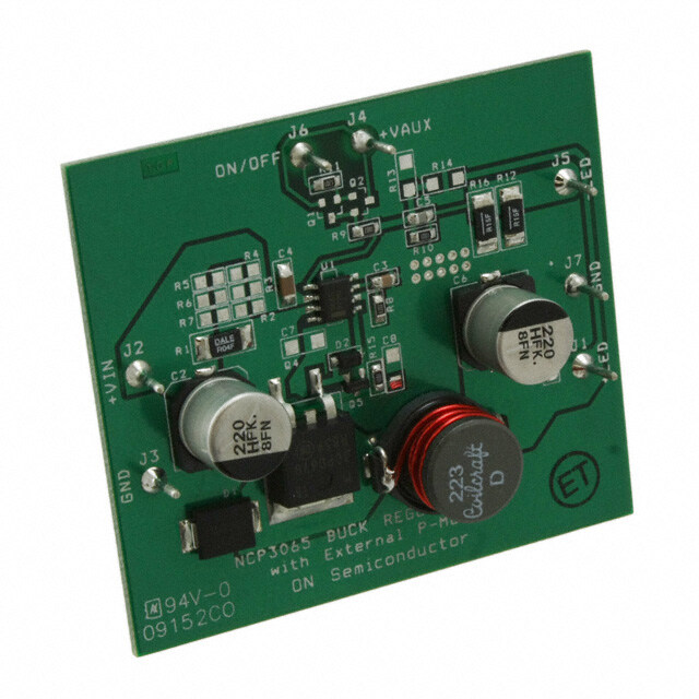
NCP30653ABCKGEVB, NCP3065SOBCKGEVB, NCP3065SOBSTGEVB High Intensity LED Drivers Using NCP3065/NCV3065 Evaluation Board User's http://onsemi.com Manual EVAL BOARD USER’S MANUAL Introduction to their wide forward voltage variation and steep V/I transfer High brightness LEDs are a prominent source of light and function. For applications that are powered from low have better efficiency and reliability than conventional light voltage AC sources typically used in landscape lighting or sources. Improvements in high brightness LEDs present the low voltage DC sources that may be used in automotive potential for creative new lighting solutions that offer an applications, high efficiency driver that can operate over improved lighting experience while reducing energy wide range of input voltages to drive series strings of one to demand. LEDs require constant current driver solutions due several LEDs. Figure 1. NCP3065 3A Buck Evaluation Board Figure 2. NCP3065 Buck Evaluation Board NCP3065/NCV3065 EVALUATION BOARD This evaluation board user’s manual describes a DC−DC NCP3065/NCV3065 can operate as a switcher or as a converter circuits that can easily be configured to drive controller. These options are shown bellow. LEDs at several different output currents and can be The brightness of the LEDs or light intensity is measured configured for either AC or DC input. The in Lumens and is proportional to the forward current flowing NCP3065/NCV3065 can be configured in a several driver through the LED. The light efficiency can vary with the topologies to a drive string of LEDs: be it traditional low current flowing through the LED string. power LEDs or high brightness high power LEDs such as the The NCP3065 is rated for commercial/industrial Lumileds Luxeon K2 and Rebel series, the CREE temperature ranges and the NCV3065 is automotive XLAMP 4550 or XR series, the OSRAM OSTAR, qualified. TopLED and Golden Dragon. Configurations like this are found in 12 V track lighting applications, automotive Evaluation Board Design Versions DC The evaluation boards are designed to display the full applications, and low voltage AC landscaping applications functionality and flexibility of NCP3065 as a driver to drive as well as track lighting such as under-cabinet lights and various LEDs at the low voltage AC and DC sources. The desk lamps that might be powered from standard components are selected for the 15 W LED driver off-the-shelf 5 V and 12 V wall adapters. The DC DC Semiconductor Components Industries, LLC, 2012 1 Publication Order Number: November, 2012 − Rev. 1 EVBUM2155/D
NCP30653ABCKGEVB, NCP3065SOBCKGEVB, NCP3065SOBSTGEVB application. Based on this circuit, there are many possible solutions. Each application is described by the schematic configurations with different input voltages and output and the bill of material and it has the option of LED dimming power levels that could be derived by making some minor by using an external PWM signal. components changes. Table 1 shows these different circuit Table 1. COMPONENTS CHANGES FOR DIFFERENT CONFIGURATIONS VIN ILED VF L COUT R8 LED Driver Application (V) (mA) (V) ((cid:2)H) ((cid:2)F) ((cid:3)) 12 VDC 1 W LED 10 − 14 350 3.6 47 100 12k 150 0 3k3 12 VDC 3 W LED 10 − 14 700 or 350 3.6 or 7.2 47 100 16k 150 0 12k 12 VDC 5 W LED 10 − 14 700 or 1,000 7.2 or 3.6 47 100 12k 150 0 12k 24 VDC 5 W LED 21 − 27 350 14 68 100 160k 220 0 39k 24 VDC 10 W LED 21 − 27 700 14 68 100 150k 220 0 100k BUCK 12 VAC 1 W LED 14 − 20 350 3.6 47 100 7k5 220 0 7k5 12 VAC 3 W LED 14 − 20 700 or 350 3.6 or 7.2 47 100 22k 220 0 22k 12 VAC 5 W LED 14 − 20 700 or 1,000 7.2 or 3.6 47 100 36k 220 0 100k/16k 12 VAC 5 W 14 − 20 350 14 47 100 NU 220 0 NU 12 VAC 15 W 21 − 27 1,000 14 47 100 82k COMPONENT SELECTION Inductor ripple current specification to allow higher peak to peak When selecting an inductor there is a trade off between values. This is achieved by configuring the NCP3065 in a inductor size and peak current. In normal applications the continuous conduction buck configuration with low peak to ripple current can range from 15% to 100%. The trade off peak ripple thus eliminating the need for an output filter being that with small ripple current the inductance value capacitor. The important design parameter is to keep the increases. The advantage is that you can maximize the peak current below the maximum current rating of the LED. current out of the switching regulator. Using 15% peak-to-peak ripple results in a good compromise between achieving max average output current With Output Capacitor Operation without exceeding the maximum limit. This saves space and A traditional buck topology includes an inductor followed reduces part count for applications that require a compact by an output capacitor which filters the ripple. The capacitor footprint. For the common LED currents such as the is placed in parallel with the LED or array of LEDs to lower 350 mA, 700 mA, 1,000 mA we setup inductor ripple LED ripple current. With this approach the output current to the 52.5 mA, 105 mA, 150 mA. With respect inductance can be reduced which makes the inductance these requirements we are able to select inductor value smaller and less expensive. Alternatively, the circuit could (Equation 1). be run at lower frequency with the same inductor value V (cid:3)V which improves the efficiency and expands the output L(cid:2) IN OUT(cid:4)T (eq. 1) voltage range. Equation 2 is used to calculate the capacitor (cid:2)I ON MAX size based on the amount of LED ripple. Output Capacitor No Output Capacitor Operation When you choose output capacitor we have to think about A constant current buck regulator such as the NCP3065 its value, ESR and ripple current. focuses on the control of the current through the load, not the voltage across it. The switching frequency of the NCP3065 C (cid:2) (cid:2)I (cid:2) VIN*(1(cid:3)D)*D (eq. 2) is in the range of 100 kHz − 300 kHz which is much higher OUT (cid:2)V*8*f 8*L*f2*(cid:2)V OUT than the human eye can detect. This allows us to relax the http://onsemi.com 2
NCP30653ABCKGEVB, NCP3065SOBCKGEVB, NCP3065SOBSTGEVB Current Feedback Loop the NCP3065 with dimming you can see in Figures 17 To drive LEDs in a constant current mode, the feedback and 18 and dimming linearity in the Figure 19. As you can for the regulator is taken by sensing the voltage drop across see in these figures there aren’t any delays in the rise or fall the sensing resistor R12, see Figures 3 or 9. The RC circuit edges, which give us the required dimming linearity. (R10&C5) between the sense resistor and the feedback pin improves converter transient response. The low feedback NCP3065 reference voltage of 235 mV allows the use of low power and lower cost sense resistor. Equation 3 calculates the sense NC resistor value. R1 J2 V 0.235V IPK IOUT(cid:2)RREF (cid:2) R [A] (eq. 3) +VIN + 0R10 sense sense C2 VCC J3 LED Current Sensing Resistor Value (mA) (m(cid:3)) GND COMP J5 R11 Q2 350 680 1/4W BC817−LT1G 700 330 1/4W ON/OFF 1k2 R9 R10 1000 220 1/4W 10k 1k 0805 R12 Rsense 1% Vout Figure 4. NCP3065 Dimming Solution A NCP3065 I = 350 mA 700 mA, 1000 mA Comp NCP3065 NC GND Rsense J2 R1 R9 IPK +VIN 0R10 10k + C2 VCC J3 Figure 3. NCP3065 Current Feedback GND COMP J5 R11 Q2 Dimming Possibility BC817−LT1G The emitted LED light is proportional to average output ON/OFF 1k2 R10 (LED) current. The NCP3065 is capable of analog and 1k digital PWM dimming. For the dimming we have three 0805 R12 possibilities how to create it. We basically use a PWM signal Rsense 1% with variable duty cycle for the managing output current Figure 5. NCP3065 Dimming Solution B value. The COMP or IPK pin of the NCP3065 is used to provide dimming capability. In digital input mode the PWM input signal inhibits switching of the regulator and reducing NCP3065 the average current through the LEDs. In analog input mode NC a PWM input signal is RC filtered and the resulting voltage R1 is summed with the feedback voltage thus reduces the J2 IPK average current through the LEDs Figure 6. The component +VIN 0R10 + value of the RC filter are dependent on the PWM frequency. Due to this, the frequency has to be higher. Figure 19 J3 C2 VCC illustrates the linearity of the digital dimming function with a 200 Hz digital PWM. The dimming frequency range for GND COMP J5 R11 R19 digital input mode is basically from 200 Hz to 1 kHz. For frequencies below 200Hz the human eye will see the flicker. ON/OFF 1k R10 J5 C9 The low dimming frequencies are EMI convenient and an impact to it is small. 1k LED 0805 R12 The Figure 4 shows us an example of solution A, which Rsense 1% uses the COMP pin to perform the dimming function and Figure 6. NCP3065 Dimming Solution C Figure 5 show us an example of solution B. The behavior of http://onsemi.com 3
NCP30653ABCKGEVB, NCP3065SOBCKGEVB, NCP3065SOBSTGEVB BOARD LAYOUT The layout of the evaluation board and schematic is shown below in Figure 7 and Figure7. Figure 7. Evaluation Board Layout Top (Not in Scale) Figure 8. Evaluation Board Silk Screen Top http://onsemi.com 4
NCP30653ABCKGEVB, NCP3065SOBCKGEVB, NCP3065SOBSTGEVB V 0 5 F/ 1 D (cid:2) 5 D 7 D J +LE C6220 J −LE J GN + C1 (cid:2)0.1F1206 5 1% B 21 ML G R10R 1 −223 40LT3 L H 5 0 S % O504 D1MBR 5 1 D 16R1 R0 G 1 T 8 Q4P06VT4G D2 MMSD414 R8 6k8C3 1.8nF C5 100pF R10 1k0805 0 3 G T MTB Q504LT1 C 9 3 T B C E P D MM R15 1k SW SW TCAC MPGN P3065C8 R14NU R13NU U1 NC PK VC CO NCSOI I C K C P N P C M I V O C 8 C F (cid:2) 1 7 0. C G + V 1 0 T R7 1206 (cid:2)1F/5 817−L R9 10k0805 2C 6 QB R6 120 0V 6 5 %R R5 120 (cid:2)F/ G 0 1 R4 206 C2+ 220 −LT1 Q1 R 1 7 1 R3 206 C80 6 R2 12061 C4 (cid:2)0.1F B R1 R04 X R11 1k2FF0805 R11 1k2FF0805 0 N D U O O J2 +VI J3 GN J4 +VA J6 ON/ J6 ON/ Figure 9. NCP3065 3A Buck Evaluation Board Schematic http://onsemi.com 5
NCP30653ABCKGEVB, NCP3065SOBCKGEVB, NCP3065SOBSTGEVB 1 D 5 D 7 D J E J E J N +L 6U −L G + CN C1 (cid:2)0.1F1206 G 3 T L L1 40 % 1 1 S (cid:5) D1 MBR R12R sense 8 Q4955T1G D2 MMSD414 R8 15kC3 1.8nF C5 100pF R10 1k0805 2 F T G T N 1 C 5T QL 4 0 9 3 T B C E P D MM R15 1k SW SW TCAC MPGN P3065C8 R14NU R13NU U1 NC PK VC CO NCSOI I C K C P N P C M I V O C 6 R7 120 6 0 G R6 12 V T1 R5 1206 F/50 17−L R9 10k R4 1206 C2+ (cid:2)220 Q2BC8 6 R3 120 G (cid:5)1%R R2 1206 C4 (cid:2)0.1F −LGT1 Q1 R0 807 1 C 6x R1 10 B R 0 1 2 1 2 1 k 1 k R 1 R 1 F F X F F N D U O O J2 +VI J3 GN J4 +VA J6 ON/ J6 ON/ Figure 10. NCP3065 Buck Evaluation Board Schematic http://onsemi.com 6
NCP30653ABCKGEVB, NCP3065SOBCKGEVB, NCP3065SOBSTGEVB Table 2. BILL OF MATERIAL FOR THE NCP3065 3A BUCK EVALUATION BOARD* Manufacturer Substitution Designator Qty. Description Value Tolerance Footprint Manufacturer Part Number Allowed U1 1 DC-DC Controller NCP3065 − SOIC8 ONSemiconductor NCP3065DR2G No C1, C4 2 Ceramic Capacitor 100nF 10% 1206 Kemet C1206F104K1RAC Yes C2, C6 2 Electrolytic Capacitor 220(cid:2)F/50V 10% G, 1010.2 Panasonic EEEVFK1H221P Yes C3 1 Ceramic Capacitor 1.8nF 10% 0805 AVX 08055F182K4Z2A Yes C5 1 Ceramic Capacitor 100pF 5% 0805 AVX 08051A101JAT2A Yes D1 1 Schottky Rectifier 5A, 40V − SMC ONSemiconductor MBRS540LT3G No D2 1 Switching Diode MMSD4148 − SOD123 ONSemiconductor MMSD4148T1G No L1 1 Surface Mount Power 22(cid:2)H 20% − Coilcraft DO5040H−223MLB Yes Inductor Q4 1 Power MOSFET, MTB30P06V − D2PAK ONSemiconductor MTB30P06VT4G No P-channel Q5 1 General Purpose MMBT3904 − SOT23 ONSemiconductor MMBT3904LT1G No Transistor R1 1 Resistor 40m(cid:3), 0.5W 1% 2010 Vishay/Dale WSL−2010.04 1% EB E3 Yes R8 1 Resistor 12k(cid:3) 1% 0805 Phycomp 232273461202 Yes R9 1 Resistor 10k(cid:3) 1% 0805 Phycomp 232273461003 Yes R10, R15 2 Resistor 1k(cid:3) 1% 0805 Phycomp 232273461002 Yes R11 1 Resistor 1.2k(cid:3) 1% 0805 Phycomp 232273461202 Yes R12, R16 2 Resistor 150m(cid:3) 1% 2010 Vishay/Dale WSL−2010.15 1% EB E3 Yes VIN, GND, 7 Test Post − − − Vector Electronics K24C/M Yes ON/OFF, VAUX, LED+, LED− Q1 1 Transistor PNP BC807 − SOT23 ONSemiconductor BC807−40LT1G Yes Q2 1 Transistor NPN BC817 − SOT23 ONSemiconductor BC817−40LT1G Yes *All devices are Pb-free. Table 3. BILL OF MATERIAL FOR THE NCP3065 BUCK EVALUATION BOARD* Manufacturer Substitution Designator Qty. Description Value Tolerance Footprint Manufacturer Part Number Allowed U1 1 DC−DC Controller NCP3065 − SOIC8 ONSemiconductor NCP3065DR2G No C2 1 Capacitor 220uF/50V 20% G, 1010.2 Panasonic EEEVFK1H221P Yes C3 1 Ceramic Capacitor 1.8nF 10% 0805 AVX 08055F182K4Z2A Yes C5 1 Ceramic Capacitor 100pF 5% 0805 AVX 08051A101JAT2A Yes C6 1 Electorlytic Capacitor 100(cid:2)F, 50V 20% F, 810.2 Panasonic EEEVFK1H101P Yes D1 1 Schottky Rectifier 1A, 40V − SMB ONSemiconductor MBRS140LT3G No D2 1 Switching Diode MMSD4148 − SOD123 ONSemiconductor MMSD4148T1G No L1 1 Surface Mount Power 47(cid:2)F 20% − Coilcraft DO3316P−473MLD Yes Inductor Q4 1 Power MOSFET, NTF2955 − SOT223 ONSemiconductor NTF2955T1G No P-channel Q5 1 General Purpose MMBT3904 − SOT23 ONSemiconductor MMBT3904LT1G No Transistor R1 1 Resistor 100m(cid:3), 0.5W 1% 2010 VISHAY DALE WSL−2010.1 1% EB E3 Yes R8 1 Resistor 12k(cid:3) 1% 0805 PHYCOMP 232273461202 Yes R9 1 Resistor 10k(cid:3) 1% 0805 PHYCOMP 232273461003 Yes R10, R15 2 Resistor 1k(cid:3) 1% 0805 PHYCOMP 232273461002 Yes R11 1 Resistor 1.2k(cid:3) 1% 0805 PHYCOMP 232273461202 Yes R12 1 Resistor 680m(cid:3) 1% 1206 PHYCOMP 235051916807 Yes *All devices are Pb-free. http://onsemi.com 7
NCP30653ABCKGEVB, NCP3065SOBCKGEVB, NCP3065SOBSTGEVB T U 1 P J T U O D E 2 C1(cid:2)1F1206 L J4 Jumper R8(cid:3)0.681206 3 1 L1 2040LT J3 Jumper R7(cid:3)0.681206 S R D1 MB R6(cid:3)0.681206 R2 F C5 100pF R5 1k0805 n 2 8 C 1. T C C E P D W W A N 5 S S TCC MPG P306C8 U1 NC PK VC CO NCSOI I P M O C W R1 R/0.5 35V 5 F/ 1 (cid:2) 0. 320 + C2 F n C4 100 1GR4 10k0805 VCC S2040LT3 S2040LT3 CC Q1BC817−LT R R V 3 B 5 B D M D M 3 3 040LT 040LT R3 1k20805 2 2 S S R R 2 B 4 B D M D M 3 2 N J O C Figure 11. Schematic NCP3065 as Switcher in the AC Input LED Driver Application http://onsemi.com 8
NCP30653ABCKGEVB, NCP3065SOBCKGEVB, NCP3065SOBSTGEVB Table 4. 12 V INPUT 1 W LED DRIVER WITHOUT OUTPUT CAPACITOR BILL OF MATERIALS DC Qty Reference Part Description Mfg P/N Mfg Package Mtg 2 C1, C4 100 nF, Ceramic Capacitor − − 1206 SMD 1 C2 220 (cid:2)F/50 V, Electrolytic Capacitor EEEVFK1H221P Panasonic G, 1010.2 SMD 1 C3 1.8 nF, Ceramic Capacitor − − 0805 SMD 1 C5 100 pF, Ceramic Capacitor − − 0805 SMD 1 D1 1 A, 40 V Schottky Rectifier MBRS140LT3G ON Semiconductor SMB SMD 1 D2 Switching Diode MMSD4148T1G ON Semiconductor SOD123 SMD 1 L1 Surface Mount Power Inductor DO3340P−154MLD Coilcraft − SMD 1 Q4 Power MOSFET, P-channel NTF2955T1G ON Semiconductor SOT223 SMD 1 Q5 General Purpose Transistor MMBT3904LT1G ON Semiconductor SOT23 SMD 1 R1 100m(cid:3), 0.5W − − 2010 SMD 1 R8 3k3, Resistor − − 0805 SMD 1 R9 10k(cid:3), Resistor − − 0805 SMD 2 R10, R15 1k(cid:3), Resistor − − 0805 SMD 1 R11 1.2k(cid:3), Resistor − − 0805 SMD 1 R12 680m(cid:3), 1% − − 1206 SMD 1 U1 DC−DC Controller NCP3065 ON Semiconductor SOIC8 SMD Table 5. 12 V INPUT 1 W LED DRIVER WITH OUTPUT CAPACITOR BILL OF MATERIALS DC Qty Reference Part Description Mfg P/N Mfg Package Mtg 2 C1, C4 100nF, Ceramic Capacitor − − 1206 SMD 1 C2 220 (cid:2)F/50 V, Electrolytic Capacitor EEEVFK1H221P Panasonic G, 1010.2 SMD 1 C3 1.8 nF, Ceramic Capacitor − − 0805 SMD 1 C5 100 pF, Ceramic Capacitor − − 0805 SMD 1 C6 100 (cid:2)F/50 V, Electrolytic Capacitor EEEVFK1H101P Panasonic F, 810.2 SMD 1 D1 1 A, 40 V Schottky Rectifier MBRS140LT3G ON Semiconductor SMB SMD 1 D2 Switching Diode MMSD4148T1G ON Semiconductor SOD123 SMD 1 L1 Surface Mount Power Inductor DO3316P−473MLD Coilcraft − SMD 1 Q4 Power MOSFET, P-channel NTF2955T1G ON Semiconductor SOT223 SMD 1 Q5 General Purpose Transistor MMBT3904LT1G ON Semiconductor SOT23 SMD 1 R1 100m(cid:3), 0.5W − − 2010 SMD 1 R8 12k, Resistor − − 0805 SMD 1 R9 10k(cid:3), Resistor − − 0805 SMD 2 R10, R15 1k(cid:3), Resistor − − 0805 SMD 1 R11 1.2k(cid:3) Resistor − − 0805 SMD 1 R12 680m(cid:3), 1% − − 1206 SMD 1 U1 DC−DC Controller NCP3065 ON Semiconductor SOIC8 SMD Table 6. 12 V INPUT 1 W LED DRIVERS TEST RESULTS DC Test Result Efficiency With Output Cap 74% Without Output Cap 72% Line regulation 3% Output Current Ripple With Output Cap <50mA Without Output Cap <100mA http://onsemi.com 9
NCP30653ABCKGEVB, NCP3065SOBCKGEVB, NCP3065SOBSTGEVB Table 7. 12 V INPUT 3 W LED DRIVER WITHOUT OUTPUT CAPACITOR BILL OF MATERIALS DC Qty Reference Part Description Mfg P/N Mfg Package Mtg 2 C1, C4 100nF, Ceramic Capacitor − − 1206 SMD 1 C2 220 (cid:2)F/50 V, Electrolytic Capacitor EEEVFK1H221P Panasonic G, 1010.2 SMD 1 C3 1.8 nF, Ceramic Capacitor − − 0805 SMD 1 C5 100 pF, Ceramic Capacitor − − 0805 SMD 1 D1 2 A, 40 V Schottky Rectifier MBRS240LT3G ON Semiconductor SMB SMD 1 D2 Switching Diode MMSD4148T1G ON Semiconductor SOD123 SMD 1 L1 Surface Mount Power Inductor DO3340P−154MLD Coilcraft − SMD 1 Q4 Power MOSFET, P-channel NTF2955T1G ON Semiconductor SOT223 SMD 1 Q5 General Purpose Transistor MMBT3904LT1G ON Semiconductor SOT23 SMD 1 R1 100m(cid:3), 0.5W − − 2010 SMD 1 R8 12k, Resistor − − 0805 SMD 1 R9 10k(cid:3), Resistor − − 0805 SMD 2 R10, R15 1k(cid:3), Resistor − − 0805 SMD 1 R11 1.2k(cid:3), Resistor − − 0805 SMD 1 R12 330m(cid:3), 1% − − 1206 SMD 1 U1 DC−DC Controller NCP3065 ON Semiconductor SOIC8 SMD Table 8. 12 V INPUT 3 W LED DRIVER WITH OUTPUT CAPACITOR BILL OF MATERIALS DC Qty Reference Part Description Mfg P/N Mfg Package Mtg 2 C1, C4 100nF, Ceramic Capacitor − − 1206 SMD 1 C2 220 (cid:2)F/50 V, Electrolytic Capacitor EEEVFK1H221P Panasonic G, 1010.2 SMD 1 C3 1.8 nF, Ceramic Capacitor, − − 0805 SMD 1 C5 100 pF, Ceramic Capacitor, − − 0805 SMD 1 C6 100 (cid:2)F/50 V, Electrolytic Capacitor EEEVFK1H101P Panasonic F, 8x10.2 SMD 1 D1 2 A, 40 V Schottky Rectifier MBRS240LT3G ON Semiconductor SMB SMD 1 D2 Switching Diode MMSD4148T1G ON Semiconductor SOD123 SMD 1 L1 Surface Mount Power Inductor DO3316P−473MLD Coilcraft − SMD 1 Q4 Power MOSFET, P-channel NTF2955T1G ON Semiconductor SOT223 SMD 1 Q5 General Purpose Transistor MMBT3904LT1G ON Semiconductor SOT23 SMD 1 R1 100m(cid:3), 0.5W − − 2010 SMD 1 R8 16k, Resistor − − 0805 SMD 1 R9 10k(cid:3), Resistor − − 0805 SMD 2 R10, R15 1k(cid:3), Resistor − − 0805 SMD 1 R11 1.2k(cid:3), Resistor − − 0805 SMD 1 R12 330m(cid:3), 1% − − 1206 SMD 1 U1 DC−DC Controller NCP3065 ON Semiconductor SOIC8 SMD Table 9. 12 V INPUT 3 W LED DRIVERS TEST RESULTS DC Test Result Efficiency With Output Cap 76% Without Output Cap 76% Line regulation 5% Output Current Ripple With Output Cap < 50 mA Without Output Cap < 90 mA http://onsemi.com 10
NCP30653ABCKGEVB, NCP3065SOBCKGEVB, NCP3065SOBSTGEVB Table 10. 12 V INPUT 5 W LED DRIVER WITHOUT OUTPUT CAPACITOR BILL OF MATERIALS DC Qty Reference Part Description Mfg P/N Mfg Package Mtg 2 C1, C4 100nF, Ceramic Capacitor − − 1206 SMD 1 C2 220 (cid:2)F/50 V, Electrolytic Capacitor EEEVFK1H221P Panasonic G, 1010.2 SMD 1 C3 1.8 nF, Ceramic Capacitor − − 0805 SMD 1 C5 100 pF, Ceramic Capacitor − − 0805 SMD 1 D1 2 A, 40 V Schottky Rectifier MBRS240LT3G ON Semiconductor SMB SMD 1 D2 Switching Diode MMSD4148T1G ON Semiconductor SOD123 SMD 1 L1 Surface Mount Power Inductor DO3340P−154MLD Coilcraft − SMD 1 Q4 Power MOSFET, P-channel NTF2955T1G ON Semiconductor SOT223 SMD 1 Q5 General Purpose Transistor MMBT3904LT1G ON Semiconductor SOT23 SMD 1 R1 100m(cid:3), 0.5W − − 2010 SMD 1 R8 12k, Resistor − − 0805 SMD 1 R9 10k(cid:3), Resistor − − 0805 SMD 2 R10, R15 1k(cid:3), Resistor − − 0805 SMD 1 R11 1.2k(cid:3), Resistor − − 0805 SMD 1 R12 220m(cid:3), 1% − − 1206 SMD 1 U1 DC−DC Controller NCP3065 ON Semiconductor SOIC8 SMD Table 11. 12 V INPUT 5 W LED DRIVER WITH OUTPUT CAPACITOR BILL OF MATERIALS DC Qty Reference Part Description Mfg P/N Mfg Package Mtg 2 C1, C4 100nF, Ceramic Capacitor − − 1206 SMD 1 C2 220 (cid:2)F/50 V, Electrolytic Capacitor EEEVFK1H221P Panasonic G, 1010.2 SMD 1 C3 1.8n F, Ceramic Capacitor, − − 0805 SMD 1 C5 100 pF, Ceramic Capacitor, − − 0805 SMD 1 C6 100 (cid:2)F/50 V, Electrolytic Capacitor EEEVFK1H101P Panasonic F, 810.2 SMD 1 D1 2 A, 40 V Schottky Rectifier MBRS240LT3G ON Semiconductor SMB SMD 1 D2 Switching Diode MMSD4148T1G ON Semiconductor SOD123 SMD 1 L1 Surface Mount Power Inductor DO3316P−473MLD Coilcraft − SMD 1 Q4 Power MOSFET, P Channel NTF2955T1G ON Semiconductor SOT223 SMD 1 Q5 General Purpose Transistor MMBT3904LT1G ON Semiconductor SOT23 SMD 1 R1 100m(cid:3), 0.5W − − 2010 SMD 1 R8 15k, resistor − − 0805 SMD 1 R9 10k(cid:3), resistor − − 0805 SMD 2 R10, R15 1k(cid:3), resistor − − 0805 SMD 1 R11 1.2k(cid:3), resistor − − 0805 SMD 1 R12 220m(cid:3), 1% − − 1206 SMD 1 U1 DC−DC controller NCP3065 ON Semiconductor SOIC8 SMD Table 12. 12 V INPUT 5 W LED DRIVERS TEST RESULTS DC Test Result Efficiency 75% Line regulation 4% Output Current Ripple With Output Cap <50mA Without Output Cap <110mA http://onsemi.com 11
NCP30653ABCKGEVB, NCP3065SOBCKGEVB, NCP3065SOBSTGEVB 400 800 390 780 380 760 370 740 A) 360 A) 720 m m (T 350 (T 700 OU 340 OU 680 I I 330 660 320 640 310 620 300 600 9 10 11 12 13 14 15 14 15 16 17 18 19 20 21 VIN (V) VIN (V) Figure 12. Current Regulation, 12 V Input Figure 13. Current Regulation, 12 V Input DC AC 1 W LED Driver 3 W LED Driver 1150 95 1100 90 1050 %) A) Y ( 85 m C (T 1000 EN OU CI 80 I 950 FI F E 900 75 850 70 10 11 12 13 14 14 15 16 17 18 19 20 VIN (V) VIN (V) Figure 14. Current Regulation, 12 V Input Figure 15. 12 V Input 5 W LED Driver DC AC 5 W LED Driver Efficiency http://onsemi.com 12
NCP30653ABCKGEVB, NCP3065SOBCKGEVB, NCP3065SOBSTGEVB Figure 16. 12 VDC, IOUT = 350 mA Input Inductor Ripple Without Output Capacitor, C1 Inductor Input, C4 Inductor Current Table 13. BUCK EFFICIENCY RESULTS FOR DIFFERENT RIPPLE WITH NO OUTPUT CAPACITOR Efficiency 1 LED, Vf = 3.6 V 2 LEDs, Vf = 3.6 V 4 LED, Vf = 14.4 V VIN = 12 VDC IOUT = 350 mA > 74% > 83% − IOUT = 700 mA > 76% > 83% − IOUT = 1,000 mA > 75% − − VIN = 12 VAC IOUT = 350 mA > 70% > 80% > 87% IOUT = 700 mA > 72% > 82% − IOUT = 1,000 mA > 70% − − VIN = 24 VDC IOUT = 350 mA − − > 82% IOUT = 700 mA − − > 86% IOUT = 1,000 mA − − > 87% http://onsemi.com 13
NCP30653ABCKGEVB, NCP3065SOBCKGEVB, NCP3065SOBSTGEVB Figure 17. NCP3065 Behavior with Dimming, Figure 18. NCP3065 Dimming Behavior, Frequency is 200 Hz, Duty Cycle 50% Frequency 1 kHz, Duty Cycle 50% 800 24 VIN, 700 VF 3.6 V 600 500 A) (mED 400 V2F4 7V.2IN V, IL 300 12 VIN, VF 3.6 V 200 100 0 0 10 20 30 40 50 60 70 80 90 100 DUTY CYCLE (%) Figure 19. Output Current Dependency on the Dimming Duty Cycle Pulse Feedback Design The NCP3065 is a burst-mode architecture product which circuit will reduce this overshoot. This will result in a is similar but not exactly the same as a hysteretic stabilized switching frequency and reduce the overshoot and architecture. The output switching frequency is dependent output ripple. The pulse feedback circuit is implemented by on the input and output conditions. The NCP3065 oscillator adding an external resistor R8 between the CT pin and generates a constant frequency that is set by an external inductor input as shown in the buck schematic Figure 9. capacitor. This output signal is then gated by the peak The resistor value is dependent on the input/output current comparator and the oscillator. When the output conditions and switching frequency. The typical range is 3k current is above the threshold voltage the switch turns off. to 200k. Table 1 contains a list of typical applications and the When the output current is below the threshold voltage the recommended value for the pulse feedback resistor. Using switch is turned on and gated with the oscillator. A an adjustable resistor in place of R8 when evaluating an simplified schematic is shown in Figure 20. This may cause application will allow the designer to optimize the value and possible overshoots on the output. Using the pulse feedback make a final selection. http://onsemi.com 14
NCP30653ABCKGEVB, NCP3065SOBCKGEVB, NCP3065SOBSTGEVB Oscillator Output from Peak Current Comparator LED Vref + − VSENSE Figure 20. Burst-Mode Architecture Figures 21 and 22 show the effect of the pulse feedback output voltage ratio. When the ratio (V /V ) is near 1 OUT IN resistor on the switching waveforms and load current ripple. (high duty cycle) over the entire input voltage range, the This results in a fixed frequency switching with constant pulse feedback is not needed. duty cycle, which is only dependent upon the input and Figure 21. Switching Waveform Without Pulse Figure 22. Switching Waveform With Pulse Feedback Feedback BOOST CONVERTER EVALUATION BOARD Boost Converter Topology The Boost converter schematic is illustrated in Figure 24. When the low side power switch is turned on, current drawn from the input begins to flow through the inductor and the current I rises up. When the low side switch is turned off, ton the current I circulates through diode D1 to the output toff capacitor and load. At the same time the inductor voltage is added with the input power supply voltage and as long as this is higher than the output voltage, the current continues to flow through the diode. Provided that the current through the inductor is always positive, the converter is operating in continuous conduction mode (CCM). On the next switching cycle, the process is repeated. Figure 23. NCP3065 Boost Evaluation Board http://onsemi.com 15
NCP30653ABCKGEVB, NCP3065SOBCKGEVB, NCP3065SOBSTGEVB J1 UT J3 ND J5 ED O G L V − + F/ 1(cid:2) C0V 00 + 15 F (cid:2) 2 1 C 0. G 3 T L 0 D1 14 G S 1 R VT MB C4 2.2nF D2 MM3Z36 e s n R9Rse C E P D W W A N 5 S S C G 06 T P P3 L1 U1 NC IPK VCC COM NC R8 1k0 7 R G 1 R6 5V H 0LT 2 (cid:2) 4 (cid:5)1% R5 (cid:2)0F/ 100 817− R11 NU R0 R4 C3+ 33 Q2BC 1 x 3 6 R F (cid:2) R2 C5 0.1 Q1 1 5 R 1 R 0 0 2 1 k R 1 F X F N D U O J2 +VI J4 GN J6 +VA J7 ON/ Figure 24. NCP3065 Boost Evaluation Board Schematic http://onsemi.com 16
NCP30653ABCKGEVB, NCP3065SOBCKGEVB, NCP3065SOBSTGEVB When operating in CCM the output voltage is equal to When the pin voltage is higher than 0.235 V the switch transistor is off. You could connect an external PWM signal 1 VOUT(cid:2)VIN(cid:6)1(cid:3)D (eq. 4) to pin ON/OFF and a power source to pin +VAUX to realize the PWM dimming function. When the dimming signal The duty cycle is defined as exceeds the turn on threshold of the external PNP or NPN t t transistor, the comp pin will be pulled up. A TTL level input D(cid:2)t (cid:7)ONt (cid:2) OTN (eq. 5) can also be used for dimming control. The range of the ON OFF dimming frequency is from 100 Hz to 1 kHz, but it is The input ripple current is defined as recommended to use frequency around 200 Hz as this is D safely above the frequency where the human eye can detect (cid:2)I(cid:2)VINf*L (eq. 6) the pulsed behavior, in addition this value is convenient to minimize EMI. There are two options to determine the The load voltage must always be higher than the input dimming polarity. The first one uses the NPN switching voltage. This voltage is defined as transistor and the second uses a PNP switching transistor. Vload(cid:2)Vsense(cid:7)n*Vf (eq. 7) The switch on/off level is dependent upon the chosen dimming topology. The external voltage source (V ) AUX where V =LED forward voltage, V is the converter f sense should have a voltage ranging from +5 V to +V . DC IN reference voltage, and n=number of LED’s in cluster. Figure 19 illustrates average LEDs current dependency on Since the converter needs to regulate current independent the dimming input signal duty cycle. of load voltage variation, a sense resistor is placed across the For cycle by cycle switch current limiting a second feedback voltage. This drop is calculated as comparator is used which has a nominal 200 mV threshold. Vsense(cid:2)Iload(cid:7)n*Rsense (eq. 8) The value of resistor R1 determines the current limit value and is configured according to the following equation. The V corresponds to the internal voltage reference or sense feedback comparator threshold. I (cid:2) 0.2 (cid:2)1.33A (eq. 10) pk(SW) 0.15 Simple Boost 350 mA LED Driver The maximum output voltage is clamped with an external The NCP3065 boost converter is configured as a LED zener diode, D2 with a value of 36 V which protects the driver is shown in Figure 24. It is well suited to automotive NCP3065 output from an open LED fault. or industrial applications where limited board space and a The evaluation board has a few options to configure it to high voltage and high ambient temperature range might be your needs. You can use one 150 m(cid:3) (R1) or a combination found. The NCP3065 also incorporates safety features such of parallel resistors such as six 1 (cid:3) resistors (R2 − R7) for as peak switch current and thermal shutdown protection. current sense. The schematic has an external high side current sense To evaluate the functionality of the board, high power resistor that is used to detect if the peak current is exceeded. LEDs with a typical V = 3.42 V @ 350 mA were connected In the constant current configuration, protection is also f in several serial combinations (4, 6, 8 LED’s string) and required in the event of an open LED fault since current will 4 chip and 6 chip LEDs with V = 14 V respectively continue to charge the output capacitor causing the output f V = 20.8 V @ 700 mA. voltage to rise. An external zener diode is used to clamp the f output voltage in this fault mode. Although the NCP3065 is Number of LEDs String Forward Voltage at 25(cid:2)C designed to operate up to 40 V additional input transient Min Typ Max protections might be required in certain automotive 4 11.16 13.68 15.96 applications due to inductive load dump. The main operational frequency is determined by the 6 16.74 20.52 23.94 external capacitor C4. The ton time is controlled by the 8 22.32 27.36 31.92 internal feedback comparator, peak current comparator and main oscillator. The output current is configured by an The efficiency was calculated by measuring the input internal feedback comparator with negative feedback input. voltage and input current and LED current and LED voltage The positive input is connected to an internal voltage drop. The output current is dependent on the peak current, reference of 0.235 V with 10% precision over temperature. inductor value, input voltage and voltage drop value and of The nominal LED current is setup by a feedback resistor. course on the switching frequency. (cid:8) (cid:9) This current is defined as: I V (cid:3)V I (cid:2) 0.235 (eq. 9) IOUT(cid:2)(D(cid:3)D2)* pkD(SW)(cid:3) IN2*L*SWf CE [A] (eq. 11) OUT R sense There are two approaches to implement LED dimming. D(cid:2) VOUT(cid:7)VF(cid:3)VIN [(cid:3)] (eq. 12) Both use the negative comparator input as a shutdown input. V (cid:7)V (cid:3)V OUT F SWCE http://onsemi.com 17
NCP30653ABCKGEVB, NCP3065SOBCKGEVB, NCP3065SOBSTGEVB Where: the regulated current to drop, Region2 is where the current V Output Voltage is flat and represents normal operation, Region3 occurs OUT V Input Voltage when V is greater than V and there is no longer IN IN OUT V Schottky Diode Forward Voltage constant current regulation. Region3 and 1 are included F V Switch Voltage Drop here for illustrative purposes as this is not a normal mode of SWCE I Peak Switch Current operation. pk(SW) D Duty Cycle Figure 11 illustrates the additional circuitry required to L Inductor Value support 12 V input signal which includes the addition of AC f Switching Frequency a bridge rectifier and input filter capacitor. The rectified dc voltage is Line regulation curve in Figure26 illustrates three distinct (cid:10) regions; in the first region, the peak current to the switch is V (cid:2) 2*V (cid:11)17V (eq. 13) INDC AC DC exceeded tripping the overcurrent protection and causing 95 400 390 90 Boost 4LED 350 mA 380 Boost 6LED 350 mA %) 370 Boost 4LED 350 mA Boost 6LED 350 mA Y ( 85 A) 360 C m EN (D 350 FICI 80 LOA 340 F I E 330 75 320 310 70 300 6 8 10 12 14 16 18 20 22 6 8 10 12 14 16 18 20 22 VIN (V) VIN (V) Figure 25. Boost Converter Efficiency for 4 or Figure 26. Line Regulation for 4 or 6 LEDs and 6 LEDs and Output Current 350 mA Output Current 350 mA Table 14. BILL OF MATERIAL FOR THE NCP3065 BOOST EVALUATION BOARD* Manufacturer Substitution Designator Qty. Description Value Tolerance Footprint Manufacturer Part Number Allowed U1 1 DC-DC Controller NCP3065 − SOIC8 ONSemiconductor NCP3065DR2G No C1 1 Electrolytic 100(cid:2)F/50V 20% F, 810.2 Panasonic EEEVFK1H101P Yes Capacitor C2, C5 2 Ceramic Capacitor 100nF 10% 1206 Kemet C1206F104K1RAC Yes C3 1 Electrolytic 220(cid:2)F/50V 20% G, 1010.2 Panasonic EEEVFK1H221P Yes Capacitor C4 1 Ceramic Capacitor 2.2nF 10% 0805 AVX 08055F222KAT2A Yes D1 1 Schottky Rectifier 1A, 40V − SMB ONSemiconductor MBRS140LT3G No D2 1 Zener Diode 36V − SOD123 ONSemiconductor MM3Z36VT1G No L1 1 Surface Mount 100(cid:2)H 20% − Coilcraft DO3340P−104MLD Yes Power Inductor Q2 1 General Purpose BC817 − SOT23 ONSemiconductor BC817−40LT1G No Transistor R1 1 Resistor 150m(cid:3), 0.5W 1% 2010 VISHAY DALE WSL−2010.15 1% EB E3 Yes R8 1 Resistor 1k(cid:3) 1% 0805 PHYCOMP 232273461002 Yes R9 1 Resistor 680m(cid:3) 1% 1206 PHYCOMP 235051916807 Yes R10 1 Resistor 1.2k(cid:3) 1% 0805 PHYCOMP 232273461202 Yes *All devices are Pb-free. http://onsemi.com 18
NCP30653ABCKGEVB, NCP3065SOBCKGEVB, NCP3065SOBSTGEVB Conclusion configured for a variety of constant current buck and boost LEDs are replacing traditional incandescent and halogen LED driver applications. In addition there is an EXCEL tool lighting sources in architectural, industrial, residential and at the ON Semiconductor website for calculating inductor the transportation lighting. The key challenge in powering and other passive components if the design requirements LED’s is providing a constant current source. The differ from the specific application voltages and currents evaluation board for the NCP3065/NCV3065 can be easily illustrated in these example. TEST PROCEDURE FOR THE NCP3065 3A BUCK EVALUATION BOARD + A − REGULATED DC ELECTRONIC V V SUPPLY LOAD − A + Figure 27. Test Setup for the NCP3065 3A Buck Evaluation Board Required Equipment Test Procedure DC Voltage Supply, Up to 35V, 4A 1.Connect the test setup as shown in Figure27. Voltage Meter 2.Apply VOUT=3.6V load. 3.Apply an input voltage, V =12V. Current Meter CC 4.Check that I is 3,000mA. OUT Electronic Load 5.Power down the V . CC 6.Power down the load. 7.End of test. TEST PROCEDURE FOR THE NCP3065 BUCK EVALUATION BOARD + A − REGULATED DC ELECTRONIC V V SUPPLY LOAD − A + Figure 28. Test Setup for the NCP3065 Buck Evaluation Board Required Equipment Test Procedure DC Voltage Supply, Up to 35V, 3A 1.Connect the test setup as shown in Figure28. Voltage Meter 2.Apply VOUT=3.6V load. 3.Apply an input voltage, V =12V. Current Meter CC 4.Check that I is 350mA. OUT Electronic Load 5.Power down the V . CC 6.Power down the load. 7.End of test. http://onsemi.com 19
NCP30653ABCKGEVB, NCP3065SOBCKGEVB, NCP3065SOBSTGEVB TEST PROCEDURE FOR THE NCP3065 BOOST EVALUATION BOARD + A − REGULATED DC V SUPPLY ELECTRONIC V LOAD − A + Figure 29. Test Setup for the NCP3065 Boost Evaluation Board Required Equipment Test Procedure DC Voltage Supply, Up to 35V, 3A 1.Connect the test setup as shown in Figure29. Voltage Meter 2.Apply VOUT=20V load. 3.Apply an input voltage, V =12V. Current Meter CC 4.Check that I is 350mA. OUT Electronic Load 5.Power down the V . CC 6.Power down the load. 7.End of test. LUXEON is a registered trademark of Philips Lumileds Lighting Company and Royal Philips Electronics of the Netherlands. OSTAR, TopLED, and Golden DRAGON LED are registered trademarks of OSRAM Opto Semiconductors, Inc. XLamp is a registered trademark of Cree, Inc ON Semiconductor and are registered trademarks of Semiconductor Components Industries, LLC (SCILLC). SCILLC owns the rights to a number of patents, trademarks, copyrights, trade secrets, and other intellectual property. A listing of SCILLC’s product/patent coverage may be accessed at www.onsemi.com/site/pdf/Patent−Marking.pdf. SCILLC reserves the right to make changes without further notice to any products herein. SCILLC makes no warranty, representation or guarantee regarding the suitability of its products for any particular purpose, nor does SCILLC assume any liability arising out of the application or use of any product or circuit, and specifically disclaims any and all liability, including without limitation special, consequential or incidental damages. “Typical” parameters which may be provided in SCILLC data sheets and/or specifications can and do vary in different applications and actual performance may vary over time. All operating parameters, including “Typicals” must be validated for each customer application by customer’s technical experts. SCILLC does not convey any license under its patent rights nor the rights of others. SCILLC products are not designed, intended, or authorized for use as components in systems intended for surgical implant into the body, or other applications intended to support or sustain life, or for any other application in which the failure of the SCILLC product could create a situation where personal injury or death may occur. Should Buyer purchase or use SCILLC products for any such unintended or unauthorized application, Buyer shall indemnify and hold SCILLC and its officers, employees, subsidiaries, affiliates, and distributors harmless against all claims, costs, damages, and expenses, and reasonable attorney fees arising out of, directly or indirectly, any claim of personal injury or death associated with such unintended or unauthorized use, even if such claim alleges that SCILLC was negligent regarding the design or manufacture of the part. SCILLC is an Equal Opportunity/Affirmative Action Employer. This literature is subject to all applicable copyright laws and is not for resale in any manner. PUBLICATION ORDERING INFORMATION LITERATURE FULFILLMENT: N. American Technical Support: 800−282−9855 Toll Free ON Semiconductor Website: www.onsemi.com Literature Distribution Center for ON Semiconductor USA/Canada P.O. Box 5163, Denver, Colorado 80217 USA Europe, Middle East and Africa Technical Support: Order Literature: http://www.onsemi.com/orderlit Phone: 303−675−2175 or 800−344−3860 Toll Free USA/Canada Phone: 421 33 790 2910 Fax: 303−675−2176 or 800−344−3867 Toll Free USA/Canada Japan Customer Focus Center For additional information, please contact your local Email: orderlit@onsemi.com Phone: 81−3−5817−1050 Sales Representative http://onsemi.com EVBUM2155/D 20