ICGOO在线商城 > 集成电路(IC) > PMIC - 稳压器 - 线性 > ADP3330ARTZ-3-RL7
 Datasheet下载
- 型号: ADP3330ARTZ-3-RL7
- 制造商: Analog
- 库位|库存: xxxx|xxxx
- 要求:
| 数量阶梯 | 香港交货 | 国内含税 |
| +xxxx | $xxxx | ¥xxxx |
查看当月历史价格
查看今年历史价格
ADP3330ARTZ-3-RL7产品简介:
ICGOO电子元器件商城为您提供ADP3330ARTZ-3-RL7由Analog设计生产,在icgoo商城现货销售,并且可以通过原厂、代理商等渠道进行代购。 ADP3330ARTZ-3-RL7价格参考¥10.79-¥22.54。AnalogADP3330ARTZ-3-RL7封装/规格:PMIC - 稳压器 - 线性, Linear Voltage Regulator IC Positive Fixed 1 Output 200mA SOT-23-6。您可以下载ADP3330ARTZ-3-RL7参考资料、Datasheet数据手册功能说明书,资料中有ADP3330ARTZ-3-RL7 详细功能的应用电路图电压和使用方法及教程。
ADP3330ARTZ-3-RL7是Analog Devices Inc.推出的一款低噪声、低压差(LDO)线性稳压器,输出电压为3.0V,具有高精度和良好的负载/线路调整率。该器件采用小型TSOT-23-5封装,适合对空间要求严苛的应用。

其典型应用场景包括便携式电池供电设备,如智能手机、平板电脑和可穿戴设备,因其低静态电流有助于延长电池续航时间。此外,ADP3330ARTZ-3-RL7具备出色的电源抑制比(PSRR)和低输出噪声,非常适合为对电源噪声敏感的模拟电路供电,例如射频(RF)模块、传感器、音频放大器和精密数据转换器(ADC/DAC)。

在工业测量设备、医疗电子(如便携式监护仪)以及需要稳定低噪声电源的嵌入式系统中,该稳压器也广泛应用。其快速瞬态响应能力确保了在负载变化时输出电压的稳定性,提高了系统可靠性。同时,内置过热和过流保护功能增强了使用安全性。

总之,ADP3330ARTZ-3-RL7适用于需要高效、低噪声、高稳定性的电源管理场景,尤其适合便携式设备和精密电子系统。
| 参数 | 数值 |
| 产品目录 | 集成电路 (IC)半导体 |
| 描述 | IC REG LDO 3V 0.2A SOT23-6线性稳压器 High Acc 200mA LDO Ultralow IQ |
| 产品分类 | |
| 品牌 | Analog Devices Inc |
| 产品手册 | |
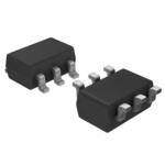
| 产品图片 |
|
| rohs | 符合RoHS无铅 / 符合限制有害物质指令(RoHS)规范要求 |
| 产品系列 | 电源管理 IC,线性稳压器,Analog Devices ADP3330ARTZ-3-RL7anyCAP® |
| 数据手册 | |
| 产品型号 | ADP3330ARTZ-3-RL7 |
| 产品种类 | |
| 供应商器件封装 | SOT-23-6 |
| 其它名称 | ADP3330ARTZ-3-RL7-ND |
| 包装 | 带卷 (TR) |
| 商标 | Analog Devices |
| 安装类型 | 表面贴装 |
| 安装风格 | SMD/SMT |
| 封装 | Reel |
| 封装/外壳 | SOT-23-6 |
| 封装/箱体 | SOT-23-6 |
| 工作温度 | -40°C ~ 85°C |
| 工厂包装数量 | 3000 |
| 最大输入电压 | 12 V |
| 最小输入电压 | 2.9 V |
| 标准包装 | 3,000 |
| 电压-跌落(典型值) | 0.14V @ 200mA |
| 电压-输入 | 最高 12V |
| 电压-输出 | 3V |
| 电流-输出 | 200mA |
| 电流-限制(最小值) | - |
| 稳压器拓扑 | 正,固定式 |
| 稳压器数 | 1 |
| 系列 | ADP3330 |
| 视频文件 | http://www.digikey.cn/classic/video.aspx?PlayerID=1364138032001&width=640&height=505&videoID=2245193149001 |
| 设计资源 | |
| 负载调节 | 0.04 mV |
| 输出电流 | 200 mA |


- 商务部:美国ITC正式对集成电路等产品启动337调查
- 曝三星4nm工艺存在良率问题 高通将骁龙8 Gen1或转产台积电
- 太阳诱电将投资9.5亿元在常州建新厂生产MLCC 预计2023年完工
- 英特尔发布欧洲新工厂建设计划 深化IDM 2.0 战略
- 台积电先进制程称霸业界 有大客户加持明年业绩稳了
- 达到5530亿美元!SIA预计今年全球半导体销售额将创下新高
- 英特尔拟将自动驾驶子公司Mobileye上市 估值或超500亿美元
- 三星加码芯片和SET,合并消费电子和移动部门,撤换高东真等 CEO
- 三星电子宣布重大人事变动 还合并消费电子和移动部门
- 海关总署:前11个月进口集成电路产品价值2.52万亿元 增长14.8%


PDF Datasheet 数据手册内容提取
High Accuracy, Ultralow I , 200 mA, Q SOT-23, anyCAP Low Dropout Regulator Data Sheet ADP3330 FEATURES SIMPLIFIED FUNCTIONAL BLOCK DIAGRAM High accuracy over line and load IN 2 Q1 1 OUT ±0.7% at +25°C ADP3330 ±1.4% over temperature THERMAL R1 PROTECTION CC Ultralow dropout voltage: 140 mV (typical) at 200 mA ERR 3 Requires only COUT= 0.47 μF for stability DRIVER gm anyCAP = stable with any type of capacitor, including R2 multilayer ceramic capacitors (MLCC) SD 6 BAND GAP REF Current and thermal limiting LLooww nshouisted own current: <2 µA GN4D 12098-001 2.9 V to 12 V supply range Figure 1. –40°C to +85°C ambient temperature range Ultrasmall, thermally enhanced, chip-on-lead™ 6-lead SOT-23 package APPLICATIONS Cell phones Notebook and palmtop computers Battery-powered systems PCMCIA regulators Bar code scanners Camcorders and cameras GENERAL DESCRIPTION The ADP3330 is a member of the Analog Devices, Inc., precision reduced to less than 2 µA. The ADP3330 has an ultralow low dropout (LDO) anyCAP® voltage regulator family of products. ground current 34 µA (typical) in light load situations. The ADP3330 operates with an input voltage range of 2.9 V to The 6-lead SOT-23 package has been thermally enhanced using 12 V and delivers a load current up to 200 mA. The ADP3330 Analog Devices proprietary chip-on-lead feature to maximize stands out from the conventional LDOs with a novel architecture power dissipation. and an enhanced process that enables it to offer performance advantages and higher output current than its competition. Its NR ERR patented design requires only a minimum output capacitor of ADP3330 0.47 µF for stability. This device is insensitive to output capacitor equivalent series resistance (ESR), and is stable with any good VIN IN OUT VOUT CIN + + COUT quality capacitor, including ceramic (MLCC) types for space 0.47µF – – 0.47µF SD GND restricted applications. The ADP3330 achieves exceptional atecmcuprearcayt uorfe ±, l0i.n7e% a natd r loooamd vtaermiapteiorantsu. rTeh aen ddr ±op1.o4u%t voovletra ge of OFFON 12098-002 the ADP3330 is only 140 mV (typical) at 200 mA. This device also Figure 2. Typical Application Circuit includes a safety current limit, thermal overload protection, and a shutdown feature. In shutdown mode, the ground current is Rev. C Document Feedback Information furnished by Analog Devices is believed to be accurate and reliable. However, no responsibility is assumed by Analog Devices for its use, nor for any infringements of patents or other One Technology Way, P.O. Box 9106, Norwood, MA 02062-9106, U.S.A. rights of third parties that may result from its use. Specifications subject to change without notice. No license is granted by implication or otherwise under any patent or patent rights of Analog Devices. Tel: 781.329.4700 ©1999–2015 Analog Devices, Inc. All rights reserved. Trademarks and registered trademarks are the property of their respective owners. Technical Support www.analog.com
ADP3330 Data Sheet TABLE OF CONTENTS Features .............................................................................................. 1 Capacitor Selection .................................................................... 11 Applications ....................................................................................... 1 Noise Reduction ......................................................................... 11 Simplified Functional Block Diagram ........................................... 1 Chip-on-Lead Package .............................................................. 11 General Description ......................................................................... 1 Thermal Overload Protection .................................................. 11 Revision History ............................................................................... 2 Calculating Junction Temperature ........................................... 12 Specifications ..................................................................................... 3 Printed Circuit Board (PCB) Layout Considerations ........... 12 ADP3330 ........................................................................................ 3 Error Flag Dropout Detector .................................................... 12 ADP3330-2.5 ................................................................................. 4 Shutdown Mode ......................................................................... 12 Absolute Maximum Ratings ............................................................ 5 Low Power, Low Dropout Applications .................................. 12 ESD Caution .................................................................................. 5 Application Circuits ....................................................................... 13 Pin Configuration and Function Descriptions ............................. 6 Crossover Switch ........................................................................ 13 Typical Performance Characteristics ............................................. 7 Higher Output Current ............................................................. 13 Theory of Operation ...................................................................... 10 Outline Dimensions ....................................................................... 14 Applications Information .............................................................. 11 Ordering Guide .......................................................................... 14 REVISION HISTORY 5/15—Rev. B to Rev. C Changes to General Description Section ...................................... 1 Changes to Chip-On-Lead Package Section ............................... 11 Changes to Ordering Guide .......................................................... 14 5/14—Rev. A to Rev. B Updated Format .................................................................. Universal Changed 0.47 mF to 0.47 µF, Features Section ............................. 1 Changes to General Description Section ...................................... 1 Changed −2.5 V to 2.5 V, ADP3330-xx Section .......................... 3 Changes to Table 1 ............................................................................ 3 Changes to Table 2 ............................................................................ 4 Changes to Figure 4 Caption through Figure 7 Caption ............. 7 Changes to Figure 10, Figure 13 Caption, Figure 14 Caption, and Figure 15 ..................................................................................... 8 Changes to Figure 16, Figure 17, and Figure 19 Caption ............ 9 Changes to Printed Circuit Board (PCB) Layout Considerations Section, and Low Power, Low Dropout Applications Section .. 12 Updated Outline Dimensions ....................................................... 14 Changes to Ordering Guide .......................................................... 14 8/99—Rev. 0 to Rev. A Rev. C | Page 2 of 16
Data Sheet ADP3330 SPECIFICATIONS ADP3330 At T = −40°C to +85°C, V = 7 V, C = 0.47 µF, C = 0.47 µF, unless otherwise noted. Ambient temperature of 85°C corresponds to a A IN IN OUT junction temperature of 125°C under typical full load test conditions. Application stable with no load. The following specifications apply to all voltage options except 2.5 V. Table 1. Parameter Symbol Test Conditions/Comments Min Typ Max Unit OUTPUT VOLTAGE ACCURACY V V = V + 0.25 V to 12 V, −0.7 +0.7 % OUT IN OUTNOM I = 0.1 mA to 200 mA, T = 25°C L A V = V + 0.25 V to 12 V, I = −1.4 +1.4 % IN OUTNOM L 0.1 mA to 150 mA, T = –40°C to +85°C A V = V + 0.25 V to 12 V, I = −1.4 +1.4 % IN OUTNOM L 0.1 mA to 200 mA, T = −20°C to +85°C A LINE REGULATION ΔV /ΔV V = V + 0.25 V to 12 V, T = 25°C 0.04 mV/V O IN IN OUTNOM A LOAD REGULATION ΔV /ΔI I = 0.1 mA to 200 mA, T = 25°C 0.04 mV/mA O L L A GROUND CURRENT I I = 200 mA, T = −20°C to +85°C 1.6 4.0 mA GND L A I = 150 mA 1.2 3.1 mA L I = 50 mA 0.4 1.1 mA L I = 0.1 mA 34 50 µA L GROUND CURRENT IN DROPOUT I V = V – 100 mV, I = 0.1 mA 37 55 µA GND IN OUTNOM L DROPOUT VOLTAGE V V = 98% of V DROP OUT OUTNOM I = 200 mA, T = −20°C to +85°C 140 230 mV L A I = 150 mA 110 170 mV L I = 10 mA 42 60 mV L I = 1 mA 25 501 mV L PEAK LOAD CURRENT I V = V + 1 V 300 mA LDPK IN OUTNOM OUTPUT NOISE2 V f = 10 Hz to 100 kHz, C = 10 µF, 47 µV rms NOISE L I = 200 mA, C = 10 nF, V = 3 V L NR OUT f = 10 Hz to 100 kHz, C = 10 µF, 95 µV rms L I = 200 mA, C = 0 nF, V = 3 V L NR OUT SHUTDOWN THRESHOLD V On 2.0 V THSD Off 0.4 V SHUTDOWN PIN INPUT CURRENT I V = 12 V, 0 V<SD ≤12 V 1.9 9 µA SD IN 0 V <SD ≤5 V 1.4 6 µA GROUND CURRENT IN SHUTDOWN MODE I SD = 0 V, V = 12 V 0.01 2 µA GNDSD IN OUTPUT CURRENT IN SHUTDOWN MODE I T = 25°C at V = 12 V 1 µA OSD A IN T = 85°C at V = 12 V 2 µA A IN ERROR PIN OUTPUT LEAKAGE I V = 5 V 1 µA EL EO ERROR PIN OUTPUT LOW VOLTAGE V I = 400 µA 0.19 0.40 V EOL SINK 1 Application stable with no load. 2 See Figure 21 and Applications Information section for additional information. Rev. C | Page 3 of 16
ADP3330 Data Sheet ADP3330-2.5 At T = −40°C to +85°C, V = 7 V, C = 0.47 µF, C = 0.47 µF, unless otherwise noted. Ambient temperature of +85°C corresponds to a A IN IN OUT junction temperature of +125°C under typical full load test conditions. Application stable with no load. Table 2. Parameter Symbol Test Conditions/Conditions Min Typ Max Unit OUTPUT VOLTAGE ACCURACY V V = 2.9 V to 12 V, −0.7 +0.7 % OUT IN I = 0.1 mA to 200 mA, T = 25°C L A V = 2.9 V to 12 V, I = 0.1 mA to −1.4 +1.4 % IN L 150 mA, T = −40°C to +85°C A V = 2.9 V to 12 V, I = 0.1 mA to −1.4 +1.4 % IN L 200 mA, T = −20°C to +85°C A LINE REGULATION ΔV /ΔV V = 2.9 V to 12 V, T = 25°C 0.04 mV/V O IN IN A LOAD REGULATION ΔV /ΔI I = 0.1 mA to 200 mA, T = 25°C 0.04 mV/mA O L L A GROUND CURRENT I I = 200 mA, T = −20°C to +85°C 1.6 4.0 mA GND L A I = 150 mA 1.2 3.1 mA L I = 50 mA 0.4 1.1 mA L I = 0.1 mA 34 50 µA L GROUND CURRENT IN DROPOUT I V = V − 100 mV, I = 0.1 mA 37 55 µA GND IN OUTNOM L DROPOUT VOLTAGE V V = 98% of V DROP OUT OUTNOM I = 200 mA, T = −20°C to +85°C 140 230 mV L A I = 150 mA 110 170 mV L I = 10 mA 42 60 mV L I = 1 mA 25 501 mV L PEAK LOAD CURRENT I V = V + 1 V 300 mA LDPK IN OUTNOM OUTPUT NOISE2 V f = 10 Hz to 100 kHz, C = 10 µF, 47 µV rms NOISE L I = 200 mA, C = 10 nF, V = 3 V L NR OUT f = 10 Hz to 100 kHz, C = 10 µF, 95 µV rms L I = 200 mA, C = 0 nF, V = 3 V L NR OUT SHUTDOWN THRESHOLD V On 2.0 V THSD Off 0.4 V SHUTDOWN PIN INPUT CURRENT I V = 12 V, 0 V<SD ≤12 V 1.9 9 µA SD IN 0 V <SD ≤5 V 1.4 6 µA GROUND CURRENT IN SHUTDOWN MODE I SD = 0 V, V = 12 V 0.01 2 µA GNDSD IN OUTPUT CURRENT IN SHUTDOWN MODE I T = 25°C at V = 12 V 1 µA OSD A IN T = 85°C at V = 12 V 2 µA A IN ERROR PIN OUTPUT LEAKAGE I V = 5 V 1 µA EL EO ERROR PIN OUTPUT LOW VOLTAGE V I = 400 µA 0.19 0.40 V EOL SINK 1 Application stable with no load. 2 See Figure 21 and Applications Information section for additional information. Rev. C | Page 4 of 16
Data Sheet ADP3330 ABSOLUTE MAXIMUM RATINGS Stresses at or above those listed under Absolute Maximum Table 3. Ratings may cause permanent damage to the product. This is a Parameter Rating stress rating only; functional operation of the product at these Input Supply Voltage −0.3 V to +16 V or any other conditions above those indicated in the operational Shutdown Input Voltage −0.3 V to +16 V section of this specification is not implied. Operation beyond Power Dissipation Internally limited the maximum operating conditions for extended periods may Operating Ambient Temperature Range −40°C to +85°C affect product reliability. Operating Junction Temperature Range −40°C to +125°C θ (4-Layer Board) 165°C/W ESD CAUTION JA θ (2-Layer Board) 190°C/W JA Storage Temperature Range −65°C to +150°C Lead Temperature (not a range) (Soldering 10 seconds) 300°C Vapor Phase (60 seconds) 215°C Infrared (15 seconds) 220°C Rev. C | Page 5 of 16
ADP3330 Data Sheet PIN CONFIGURATION AND FUNCTION DESCRIPTIONS OUT 1 6 SD ADP3330 IN 2 TOP VIEW 5 NR (Not to Scale) ERR 3 4 GND 12098-003 Figure 3. Pin Configuration Table 4. Pin Function Descriptions Pin No. Mnemonic Description 1 OUT Output of the Regulator. Bypass to ground with a 0.47 µF or larger capacitor. 2 IN Regulator Input. 3 ERR Open Collector Output. This pin goes low to indicate that the output is about to go out of regulation. 4 GND Ground Pin. 5 NR Noise Reduction Pin. This pin is used for further reduction of output noise (see the Applications Information section). Do not connect if this pin is not used. 6 SD Active Low Shutdown Pin. Connect to ground to disable the regulator output. When shutdown is not used, this pin must be connected to the input pin. Rev. C | Page 6 of 16
Data Sheet ADP3330 TYPICAL PERFORMANCE CHARACTERISTICS 3.010 1.6 VOUT = 3V VIN = 7V 3.008 1.4 3.006 V)3.004 IL = 0mA mA) 1.2 AGE (3.002 IL = 10mA ENT ( 1.0 OUTPUT VOLT232...909909608 IIILLL === 511005m00mmAAA ROUND CURR 00..86 G 0.4 2.994 IL = 200mA 0.2 2.992 2.9903.25 4 5 6 INPU7T VOLT8AGE (V9) 10 11 12 12098-004 00 50 OUTPUT1 L0O0AD (mA) 150 200 12098-007 Figure 4. Line Regulation Output Voltage vs. Input Voltage Figure 7. Ground Current vs. Output Current 3.005 0.4 VOUT = 3V IL = 0mA 3.004 VIN = 7V 3.003 0.3 IL = 50mA V)3.002 %) AGE (3.001 AGE ( 0.2 LT3.000 LT O O UT V2.999 UT V 0.1 IL = 150mA OUTP22..999987 OUTP IL = 200mA 2.996 0 2.995 2.9940 25 50 O7U5TPUT1 L0O0AD (1m2A5) 150 175 200 12098-005 –0.1–45 –25 –5JUNC15TION 3T5EMPE5R5ATUR7E5 (°C)95 115 135 12098-008 Figure 5. Output Voltage vs. Output Current Figure 8. Output Voltage Variation Percent vs. Junction Temperature 45 3.0 IL = 100µA VOUT = 3V 2.8 IL = 200mA VIN = 7V 40 2.6 35 2.4 A) A) 2.2 µ m GROUND CURRENT ( 32210505 IL = 0µA GROUND CURRENT ( 2111110.......0864208 IL = 150mA IL = 100mA 10 0.6 5 0.4 IL = 50mA 0.2 IL = 0mA 00 2 4INPUT VO6LTAGE (V)8 10 12 12098-006 0–45 –25 –5JUNC15TION 3T5EMPE5R5ATUR7E5 (°C)95 115 135 12098-009 Figure 6. Ground Current vs. Input Voltage Figure 9. Ground Current vs. Junction Temperature Rev. C | Page 7 of 16
ADP3330 Data Sheet 250 3.04 VOUT = 3V RL = 15Ω 3.02 CL = 0.47µF 200 V) V) 3.00 AGE (m 150 V (OUT 2.98 T L O 2.96 V T U 100 O 2.94 P O R D V) 7.5 50 (N VI 7.0 00 25 50 O7U5TPUT1 L0O0AD (1m2A5) 150 175 200 12098-010 6.50 100 200TIME (µs)300 400 500 12098-013 Figure 10. Dropout Voltage vs. Output Current Figure 13. Line Transient Response, CL = 0.47 µF 3.5 3.04 VOUT = 3V VOUT = 3V 3.0 SRDL == 1V5INΩ 3.02 RCLL == 1150ΩµF LTAGE (V) 22..50 V (V)OUT 32..0908 O V UT 1.5 2.96 P T OU 1.0 2.94 T/ U INP 0.5 (V)N 7.5 0 VI 7.0 –0.50 1 T2IME (Second3s) 4 5 12098-011 6.50 100 200TIME (µs)300 400 500 12098-014 Figure 11. Power-Up/Power-Down Figure 14. Line Transient Response, CL = 10 µF 4 3.10 V (V)OUT 32 CL = 0.47µF VSVDIONU ==T V7=IV N3V T VOLTAGE(V)33..0050 VCVIOLN U ==T 0 7=.V4 37VµF 1 CL = 10µF RL = 15Ω UTPU 2.95 0 O 2.90 10 200 T V (V)IN 5 CURRENmA)100 20mA 0 D ( 0 A O L –50 100 200TIME (µs)300 400 500 12098-012 –1000 200 400TIME (µs)600 800 1000 12098-015 Figure 12. Power-Up Response Figure 15. Load Transient Response, CL = 0.47 µF Rev. C | Page 8 of 16
Data Sheet ADP3330 3.10 0 VIN = 7V VOUT = 3V VOUT = 3V –10 GE 3.05 CL = 10µF VOLTAV)3.00 dB) ––3200 CILL == 00..14m7µAF UTPUT (2.95 CTION ( –40 CILL = = 2 00.04m7µAF O 2.90 JE –50 E R CURRENTmA)210000 20mA RIPPLE –––876000 CL = 10µF CILL = = 2 1000µmFA D ( 0 IL = 0.1mA A –90 O L –1000 200 400TIME (µs)600 800 1000 12098-016 –10010 100 1kFREQU1E0NkCY (Hz)100k 1M 10M 12098-019 Figure 16. Load Transient Response, CL = 10 µF Figure 19. Power Supply Ripple Rejection vs. Frequency 160 3 VOUT E 0 G 140 A LT 500 IL = 200mA O 120 VV) UTPUT (400 E (µV) 100 IL = 0mA O 300 IOUT OIS 80 N S NT 200 RM 60 WIL I=T H20 N0mOIASE REDUCTION E CURRmA)100 40 AD ( 0 20 IL = 0mA LO VIN = 7V WITH NOISE REDUCTION –1000 1 T2IME (Second3s) 4 5 12098-017 00 10 20 CL (µF) 30 40 50 12098-020 Figure 17. Short-Circuit Current Figure 20. RMS Noise vs. CL (10 Hz to100 kHz) V (V)OUT 32 VCVRIOLLN U ===T 11 7=50V Ωµ3FV TY (µV√Hz) 1 CL = 10µF CCLN R= =0 .047µF NSI CNR = 0 1 DE CL = 0.47µF V) AL CNR = 10nF (RR 0 CTR 0.1 CL = 10µF VE 3 PE CNR = 10nF 0 E S S OI (V)D 2 GE N VS 0 TA OL VOUT = 3V V IL = 200mA –20 200 400TIME (µs)600 800 1000 12098-018 0.0110 100 1kFREQU1E0NkCY (Hz)100k 1M 10M 12098-021 Figure 18. Turn On/Turn Off Response Figure 21. Output Noise Density Rev. C | Page 9 of 16
ADP3330 Data Sheet THEORY OF OPERATION The anyCAP low dropout (LDO) ADP3330 uses a single control The patented amplifier controls a new and unique noninverting loop for regulation and reference functions. The output voltage driver that drives the pass transistor, Q1. The use of this is sensed by a resistive voltage divider consisting of R1 and R2, noninverting driver enables the frequency compensation to which is varied to provide the available output voltage options. include the load capacitor in a pole splitting arrangement to Feedback is taken from this network by way of a series diode achieve reduced sensitivity to the value, type, and ESR of the (D1) and a second resistor divider (R3 and R4) to the input of load capacitance. an amplifier. Most LDOs place strict requirements on the range of ESR values INPUT OUTPUT for the output capacitor because they are difficult to stabilize, due to the uncertainty of load capacitance and resistance. Q1 CCAOPMAPCEINTSOARTION ATTENUATION R1 Moreover, the ESR value required to keep conventional LDOs (VBAND GAP/VOUT) NOWNIIDNEVBEARNTDING gm PVTOAST R3 D1 (a) CLOAD slitmabitlea tciohnans gmesa kdee pdeensidginnign go nw liotha dL DanOds t emmopree rdaitfufirceu. lTt hbeescea uEsSeR o f DRIVER R4 CUPRTRAETNT RLOAD their unclear specifications and extreme variations over R2 ADP3330 temperature. The ADP3330 anyCAP LDO overcomes these limitations. It can GND 12098-022 bcoen ussteradi nwti tohn v tihretu malilny iamnuym go EoSdR q. uTahliet yin cnapovacatitiover, dweistihg nn oa llows Figure 22. Functional Block Diagram the circuit to be stable with just a small 0.47 µF capacitor on the A very high gain error amplifier is used to control this loop. The output. Additional advantages of the pole splitting scheme amplifier is constructed in such a way that, at equilibrium, the include superior line noise rejection and very high regulator amplifier produces a large, temperature proportional input gain, which leads to excellent line and load regulation. An offset voltage that is repeatable and very well controlled. The impressive ±1.4% accuracy is guaranteed over line, load and temperature proportional offset voltage is combined with the temperature. complementary diode voltage to form a virtual band gap Additional features of the circuit include current limit, thermal voltage, implicit in the network, although it never appears shutdown, and noise reduction. Compared to standard explicitly in the circuit. Ultimately, this patented design makes it solutions that give warning after the output has lost regulation, possible to control the loop with only one amplifier. This the ADP3330 provides improved system performance by technique also improves the noise characteristics of the enabling the ERR pin to give warning just before the device amplifier by providing more flexibility on the trade-off of noise loses regulation. sources that leads to a low noise design. When the temperature of the chip rises to more than 165°C, the The R1, R2 divider is chosen in the same ratio as the band gap circuit activates a soft thermal shutdown, indicated by a signal voltage to the output voltage. Although the R1, R2 resistor low on the ERR pin, to reduce the current to a safe level. divider is loaded by the D1 diode and a second divider consisting of R3 and R4, the values are chosen to produce a temperature stable output. This unique arrangement specifically corrects the loading of the divider so that the typical error resulting from base current loading in conventional circuits is avoided. Rev. C | Page 10 of 16
Data Sheet ADP3330 APPLICATIONS INFORMATION CAPACITOR SELECTION CHIP-ON-LEAD PACKAGE Output Capacitors The ADP3330 uses a Chip-on-Lead package design (protected As with any micropower device, output transient response is a by U.S. Patent 5929514 A) to ensure the best thermal performance function of the output capacitance. The ADP3330 is stable with in the 6-lead SOT-23 footprint. In a standard 6-lead SOT-23 a wide range of capacitor values, types, and ESR (anyCAP). A package, the majority of the heat flows out of the ground pin. capacitor as low as 0.47 µF is all that is needed for stability; The Chip-on-Lead package uses an electrically isolated die larger capacitors can be used if high output current surges are attachment that allows all pins to contribute to the heat anticipated. The ADP3330 is stable with extremely low ESR conduction. This technique reduces the thermal resistance to capacitors (ESR ≈ 0), such as MLCC or OSCON. Note that the 190°C/W on a 2-layer board as compared to >230°C/W for a effective capacitance of some capacitor types may fall less than standard SOT-23 lead frame. Figure 24 and Figure 25 show the the minimum at cold temperature. Ensure that the capacitor difference between the standard 6-lead SOT-23 and the Chip-on- provides more than 0.47 µF at minimum temperature. Lead lead frames. Input Bypass Capacitor An input bypass capacitor is not strictly required, but it is advisable in any application involving long input wires or high source impedance. Connecting a 0.47 µF capacitor from IN to SILICON GboNaDrd r(ePdCuBce) sl atyhoeu ste.n Isf iati vlairtyg eorf vtahleu ec iorcuutpitu tto c parpianctietdo rc iisr cuusiet d, a DIE 12098-024 larger value input capacitor is also recommended. Figure 24. Normal 6-Lead SOT-23 Package NOISE REDUCTION A noise reduction capacitor (C ) can be used to further reduce NR the noise by 6 dB to 10 dB (see Figure 23). Low leakage capacitors in the 10 pF to 500 pF range provide the best SILICON DIE WITH ELECTRICALLY ppiecrkfourpm fraonmce .e xCtaerrenfaull lsyo ucorcnense bcet ctaou tshei st hneo ndoe itsoe arvedoiudc tnioonis ep in DIEIS AOTLTAATCEHD 12098-025 (NR) is internally connected to a high impedance node. The Figure 25. Thermally Enhanced, Chip-on-Lead Package pad connected to this pin must be as small as possible and long THERMAL OVERLOAD PROTECTION PCB traces are not recommended. The ADP3330 is protected against damage due to excessive When adding a noise reduction capacitor, use the following power dissipation by its thermal overload protection circuit, guidelines: which limits the die temperature to a maximum of 165°C. • Maintain a minimum load current of 1 mA when not in Under extreme conditions, (that is, high ambient temperature shutdown. and power dissipation) where die temperature starts to rise • For C values greater than 500 pF, add a 100 kΩ series more than 165°C, the output current decreases until the die NR resistor (R ). temperature has dropped to a safe level. The output current is NR restored when the die temperature is reduced. It is important to note that as C increases, the turn on time is NR Current and thermal limit protections protect the device against delayed. When C values are greater than 1 nF, this delay may NR accidental overload conditions. For normal operation, device be in the order of several milliseconds. power dissipation must be externally limited so that the junction temperatures do not exceed 125°C. NR ADP3330-3 CNR RNR VIN IN OUT VOUT = 3.3V 0.47CµF1 +– R3310kΩ +– C0.247µF ERR SD GND 12098-023 Figure 23. Noise Reduction Circuit Rev. C | Page 11 of 16
ADP3330 Data Sheet CALCULATING JUNCTION TEMPERATURE ERROR FLAG DROPOUT DETECTOR Device power dissipation is calculated as follows: The ADP3330 maintains its output voltage over a wide range of load, input voltage, and temperature conditions. If the output is P = (V − V ) I + (V ) I D IN OUT LOAD IN GND about to lose regulation by reducing the supply voltage less than where: the combined regulated output and dropout voltages, the ERR I and I are load current and ground current. LOAD GND flag is activated. The ERR output is an open collector that is V and V are input and output voltages, respectively. IN OUT driven low. Assuming I = 200 mA, I = 4 mA, V = 4.2 V, and V = LOAD GND IN OUT When the ERR output is set, the hysteresis of the ERR flag keeps 3.0 V, the device power dissipation is the following: the output low until a small margin of the operating range is PD = (4.2 − 3.0) 200 mA + 4.2 (4 mA) = 257 mW restored either by raising the supply voltage or reducing the load. The proprietary package used in the ADP3330 has a thermal SHUTDOWN MODE resistance of 165°C/W, significantly lower than the standard Applying a TTL high signal to the shutdown (SD) pin, or tying 6-lead SOT-23 package. Assuming a 4-layer board, the junction temperature rise above ambient temperature is approximately the SD pin to the input pin, turns the output on. Pulling the SD equal to pin down to 0.4 V or below, or tying the SD pin to ground, turns the output off (we do not do all caps for emphasis). In ΔT = 0.257 W × 165°C/W = 42.4°C JA shutdown mode, the ground current is reduced to much less To limit the maximum junction temperature to 125°C, than 1 µA. maximum allowable ambient temperature is LOW POWER, LOW DROPOUT APPLICATIONS T = 125°C − 42.4°C = 82.6°C A MAX The ADP3330 is well suited for applications such as cell phone PRINTED CIRCUIT BOARD (PCB) LAYOUT handsets that require low ground current and low dropout CONSIDERATIONS voltage features. The ADP3330 typically draws 34 µA under All packages rely on the traces of the PCB to conduct heat away light load situations (that is, load current = 100 µA), which from the package. results in low power consumption when the cell phone is in standby mode. In standard packages, the dominant component of the heat resistance path is the plastic between the die attach pad and the Figure 26 shows an application in which the ADP3330 is used individual leads. In typical thermally enhanced packages, one or in a handset to provide 2.75 V nominal output voltage. The cell more of the leads are fused to the die attach pad, significantly phone is powered from a 3 cell NiCd or 1 cell Li-Ion battery. decreasing this component. To make the improvement The ADP3330 guarantees an accuracy of 1.4%, even when the meaningful, however, a significant copper area on the PCB must input/output differential is merely 250 mV (worst case). be attached to these fused pins. Therefore, the voltage output is regulated and within specification even when the battery voltage has reached its end The patented chip-on-lead frame design of the ADP3330 of discharge voltage of 3 V. The output voltage never falls less uniformly minimizes the value of the dominant portion of the than 2.7 V, even under worst case load and temperature thermal resistance. It ensures that heat is conducted away by all conditions. The low dropout feature coupled with the high of the package pins and yields a very low 165°C/W thermal accuracy of the ADP3330 ensures that the system is reliably resistance for the 6-lead SOT-23 package. Low thermal powered until the end of the life of the battery, which results in resistance is achieved without any special board layout increased system talk time. requirements, just the normal traces connected to the leads, and END OF DISCHARGE VOLTAGE yields a 17% improvement in heat dissipation capability as OF 3 CELL NiCd OR 1 CELL Li-Ion BATTERY compared to a standard 6-lead SOT-23 package. The thermal MINIMUM BATTERY VOLTAGE 3.0V resistance can be decreased by approximately an additional 10% by attaching a few square cm of copper area to the VIN pin of the 250mV MAXIMUM INPUT-OUTPUT OVERHEAD FOR 200mA OUTPUT ADP3330 package. CURRENT It is not recommended to use solder mask or silkscreen on the NOMINAL OUTPUT VOLTAGE 2.75V PCB traces adjacent to the pins of the ADP3330 because it –1.4% OUTPUT increases the junction to ambient thermal resistance of the VOLTAGE ACCURACY package. 2.712V 12mV TRANSIENT, LINE AND ABOSUOTLPUUTTE V MOINL2TI.M7A0UG0MVE LOAD RESPECTIVE MARGIN 12098-026 Figure 26. LDO Budgeting for a 3 Cell NiCd/1 Cell Li-Ion Supply Rev. C | Page 12 of 16
Data Sheet ADP3330 APPLICATION CIRCUITS CROSSOVER SWITCH HIGHER OUTPUT CURRENT The circuit in Figure 27 shows how two ADP3330s can be used The ADP3330 can source up to 200 mA at room temperature to form a mixed supply voltage system. The output switches without any heat-sink, or pass transistor. If higher current is between two different levels selected by an external digital needed, an appropriate pass transistor can be used, as in input. Output voltages can be any combination of voltages that Figure 28, to increase the output current to 1 A. are included in the Ordering Guide. MJE253* VIN = 4.5V TO 8V VOUT = 3V AT 1A C1 VIN = 3.85V TO 12V IN OUT VOUT = 3.6V/2.5V 100µF R1 50Ω ADP3330-3.6 OUTPUT SELECT IN 3V SD OUT 0V GND + C2 ADP3330-3 100µF SD ERR GND 1.0CµF1+ AINDP3330-O2U.5T + C0.247µF *AAVID531002 HEAT-SINK IS USED 12098-028 LOGIC SUPPLY Figure 28. High Output Current Linear Regulator SD GND 12098-027 Figure 27. Crossover Switch Rev. C | Page 13 of 16
ADP3330 Data Sheet OUTLINE DIMENSIONS 3.00 2.90 2.80 1.70 6 5 4 3.00 1.60 2.80 1.50 2.60 1 2 3 PIN1 INDICATOR 0.95BSC 1.90 BSC 1.30 1.15 0.90 1.45MAX 0.20MAX 0.95MIN 0.08MIN 0.55 0.15MAX 10° 0.45 0.05MIN 0.50MAX SPELAATNIENG 4° B0S.6C0 0.35 0.30MIN 0° COMPLIANTTOJEDECSTANDARDSMO-178-AB 12-16-2008-A Figure 29. 6-Lead Small Outline Transistor Package [SOT-23] RJ-6 Dimensions shown in millimeters ORDERING GUIDE Model1 Temperature Range Voltage Output (V) Package Description Package Option2 Branding ADP3330ARTZ-2.5-R7 −40°C to +85°C 2.5 6-Lead SOT-23 RJ-6 L1B ADP3330ARTZ-2.75R7 −40°C to +85°C 2.75 6-Lead SOT-23 RJ-6 L2B ADP3330ARTZ-2.75RL −40°C to +85°C 2.75 6-Lead SOT-23 RJ-6 L2B ADP3330ARTZ-2.85R7 −40°C to +85°C 2.85 6-Lead SOT-23 RJ-6 L3B ADP3330ARTZ-3-RL7 −40°C to +85°C 3.0 6-Lead SOT-23 RJ-6 L4B ADP3330ARTZ3.3-RL7 −40°C to +85°C 3.3 6-Lead SOT-23 RJ-6 L5B ADP3330ARTZ-3.6-R7 −40°C to +85°C 3.6 6-Lead SOT-23 RJ-6 L6B ADP3330ARTZ-5-RL7 −40°C to +85°C 5.0 6-Lead SOT-23 RJ-6 L8B 1 Z = RoHS Compliant Part. 2 Contact the factory for the availability of other output voltage options. Rev. C | Page 14 of 16
Data Sheet ADP3330 NOTES Rev. C | Page 15 of 16
ADP3330 Data Sheet NOTES ©1999–2015 Analog Devices, Inc. All rights reserved. Trademarks and registered trademarks are the property of their respective owners. D12098-0-5/15(C) Rev. C | Page 16 of 16