ICGOO在线商城 > 集成电路(IC) > PMIC - AC-DC 转换器,离线开关 > NCP1337DR2G
 Datasheet下载
- 型号: NCP1337DR2G
- 制造商: ON Semiconductor
- 库位|库存: xxxx|xxxx
- 要求:
| 数量阶梯 | 香港交货 | 国内含税 |
| +xxxx | $xxxx | ¥xxxx |
查看当月历史价格
查看今年历史价格
NCP1337DR2G产品简介:
ICGOO电子元器件商城为您提供NCP1337DR2G由ON Semiconductor设计生产,在icgoo商城现货销售,并且可以通过原厂、代理商等渠道进行代购。 NCP1337DR2G价格参考。ON SemiconductorNCP1337DR2G封装/规格:PMIC - AC-DC 转换器,离线开关, Converter Offline Flyback Topology 130kHz 7-SOIC。您可以下载NCP1337DR2G参考资料、Datasheet数据手册功能说明书,资料中有NCP1337DR2G 详细功能的应用电路图电压和使用方法及教程。
ON Semiconductor(安森美)的NCP1337DR2G是一款电流模式脉冲宽度调制(PWM)控制器,属于PMIC - AC-DC转换器、离线开关类别,广泛应用于低功耗至中等功率的开关电源系统。其主要应用场景包括:

1. 消费类电子产品:常用于手机充电器、USB适配器、智能家居设备电源模块等,因其高能效和轻载高效待机特性,符合能源之星等节能标准。

2. 家电辅助电源:适用于电视、音响、微波炉等家用电器中的待机电源或控制电路供电,支持宽输入电压范围,适应全球交流电网。

3. 工业电源模块:用于小型工业设备、传感器供电、PLC辅助电源等对可靠性和稳定性要求较高的场合。

4. LED照明驱动:可作为LED灯泡或灯具的离线式恒压或恒流驱动电源方案,具备良好的动态响应和保护功能。

5. IoT设备电源:适用于各类物联网终端设备,如智能网关、无线摄像头等,满足小体积、低待机功耗的设计需求。

NCP1337DR2G采用DIP-8封装,内置软启动、过载保护、过压保护和热关断等多重安全机制,提升了系统可靠性。其准谐振(Quasi-Resonant)工作模式有效降低开关损耗,提高转换效率,是设计高效、低成本AC-DC电源的理想选择。
| 参数 | 数值 |
| 产品目录 | 集成电路 (IC)半导体 |
| Cuk | 无 |
| 描述 | IC REG CTRLR FLYBK ISO PWM 7SOIC开关控制器 PWM CONTROLLER |
| 产品分类 | |
| 品牌 | ON Semiconductor |
| 产品手册 | |
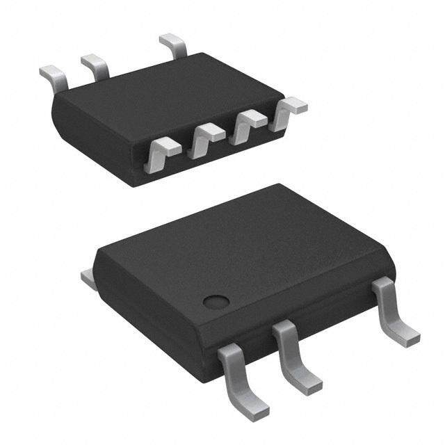
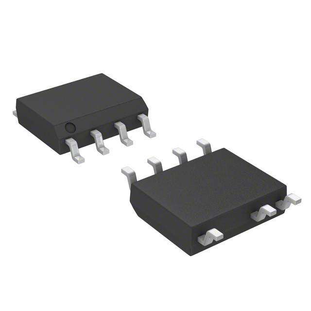
| 产品图片 |
|
| rohs | 符合RoHS无铅 / 符合限制有害物质指令(RoHS)规范要求 |
| 产品系列 | 电源管理 IC,开关控制器 ,ON Semiconductor NCP1337DR2G- |
| 数据手册 | |
| 产品型号 | NCP1337DR2G |
| PWM类型 | 电流模式 |
| 上升时间 | 50 ns |
| 下降时间 | 20 ns |
| 产品种类 | 开关控制器 |
| 倍增器 | 无 |
| 其它名称 | NCP1337DR2GOSDKR |
| 分频器 | 无 |
| 包装 | Digi-Reel® |
| 升压 | 无 |
| 占空比 | - |
| 反向 | 无 |
| 反激式 | 是 |
| 商标 | ON Semiconductor |
| 安装风格 | SMD/SMT |
| 封装 | Reel |
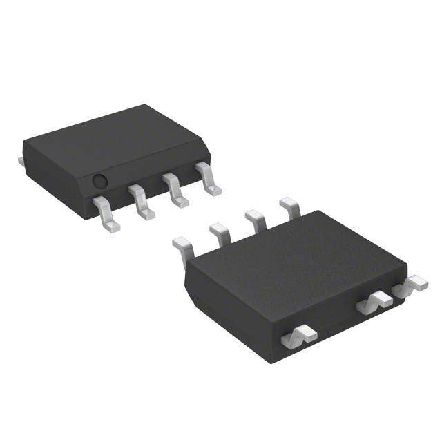
| 封装/外壳 | 8-SOIC(0.154",3.90mm 宽)7 引线 |
| 封装/箱体 | SOIC-7 |
| 工作温度 | -40°C ~ 125°C |
| 工厂包装数量 | 2500 |
| 最大工作温度 | + 125 C |
| 最小工作温度 | - 40 C |
| 标准包装 | 1 |
| 电压-电源 | 11 V ~ 20 V |
| 类型 | Current Mode PWM Controllers |
| 系列 | NCP1337 |
| 输出数 | 1 |
| 输出电流 | 500 mA |
| 输出端数量 | 1 Output |
| 配用 | /product-detail/zh/NCP1337ADAPEVB/NCP1337ADAPEVBOS-ND/2890964/product-detail/zh/NCP1337ADAPGEVB/NCP1337ADAPGEVBOS-ND/2337327 |
| 降压 | 无 |
| 隔离式 | 是 |
| 频率-最大值 | 130kHz |


- 商务部:美国ITC正式对集成电路等产品启动337调查
- 曝三星4nm工艺存在良率问题 高通将骁龙8 Gen1或转产台积电
- 太阳诱电将投资9.5亿元在常州建新厂生产MLCC 预计2023年完工
- 英特尔发布欧洲新工厂建设计划 深化IDM 2.0 战略
- 台积电先进制程称霸业界 有大客户加持明年业绩稳了
- 达到5530亿美元!SIA预计今年全球半导体销售额将创下新高
- 英特尔拟将自动驾驶子公司Mobileye上市 估值或超500亿美元
- 三星加码芯片和SET,合并消费电子和移动部门,撤换高东真等 CEO
- 三星电子宣布重大人事变动 还合并消费电子和移动部门
- 海关总署:前11个月进口集成电路产品价值2.52万亿元 增长14.8%


PDF Datasheet 数据手册内容提取
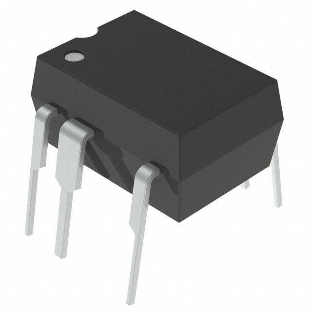
NCP1337 PWM Current-Mode Controller for Free Running Quasi-Resonant Operation The NCP1337 combines a true current mode modulator and ademagnetization detector which ensures full Borderline/Critical Conduction Mode in any load/line conditions together with www.onsemi.com minimum drain voltage switching (Quasi−Resonant operation). Thetransformer core reset detection is done internally, without using MARKING any external signal, due to the Soxyless concept. The frequency is DIAGRAM internally limited to 130 kHz, preventing the controller to operate above the 150 kHz CISPR−22 EMI starting limit. 7 By monitoring the feedback pin activity, the controller enters skip PDIP−7 NCP1337P mode as soon as the power demand falls below a predetermined P SUFFIX AWL level. As each restart is softened by an internal Soft−Skip(cid:2), and as CASE 626B YYWWG the frequency cannot go below 25 kHz, no audible noise can be 1 heard. The NCP1337 also features an efficient protective circuitry which, 8 in presence of an overcurrent condition, disables the output pulses P1337 and enters a safe burst mode, trying to restart. Once the default has SOIC−7 ALYW(cid:3) gone, the device auto−recovers. Also included is a bulk voltage D SUFFIX (cid:3) CASE 751U monitoring function (known as brown−out protection), an adjustable 1 overpower compensation, and a V OVP. The controller CC immediately restarts after any of these conditions, unless the fault A = Assembly Location timer has timed out. Finally, an internal 4.0 ms soft−start eliminates WL, L = Wafer Lot the traditional startup stress. YY, Y = Year WW, W = Work Week Features G, (cid:3) = Pb−Free Package • Free−Running Borderline/Critical Mode Quasi−Resonant Operation (Note: Microdot may be in either location) • Current−Mode • PIN CONNECTIONS Soft−Skip Mode with Minimum Switching Frequency for Standby • Auto−Recovery Short−Circuit Protection Independent of Auxiliary 1 8 BO HV Voltage 2 • Overvoltage Protection FB • 3 6 Brown−Out Protection CS VCC • Two Externally Triggerable Fault Comparators (one for a disable 4 5 GND DRV function, and the other for a permanent latch) • Internal 4.0 ms Soft−Start (Top View) • 500 mA Peak Current Drive Sink Capability • 130 kHz Max Frequency ORDERING INFORMATION • Internal Leading Edge Blanking Device Package Shipping† • Internal Temperature Shutdown • NCP1337PG PDIP−7 50 Units/Rail Direct Optocoupler Connection (Pb−Free) • Dynamic Self−Supply with Levels of 12 V (On) and 10 V (Off) • NCP1337DR2G SOIC−7 2500 Tape & Reel SPICE Models Available for TRANsient and AC Analysis (Pb−Free) • These are Pb−Free Devices †For information on tape and reel specifications, Typical Applications including part orientation and tape sizes, please • refer to our Tape and Reel Packaging Specification AC−DC Adapters for Notebooks, etc. Brochure, BRD8011/D. • Offline Battery Chargers • Consumer Electronics (DVD Players, Set−Top Boxes, TVs, etc.) • Auxiliary Power Supplies (USB, Appliances, TVs, etc.) © Semiconductor Components Industries, LLC, 2014 1 Publication Order Number: December, 2014 − Rev. 6 NCP1337/D
NCP1337 PIN FUNCTION DESCRIPTION Pin No. Symbol Function Description 1 BO Brown−out and external • By connecting this pin to the input voltage through a resistor divider, the triggering controller ensures operation at a safe mains level, thanks to a 500 mV brown−out comparator. • If an external event brings this pin above 3.0 V, the controller’s output is disabled. • If an external event brings this pin above 5.0 V, the controller is permanently latched−off. 2 FB Sets the peak current • By connecting an optocoupler or an auxiliary winding to this pin, the peak setpoint current setpoint is adjusted accordingly to the output power demand. • When the requested peak current setpoint is below the internal standby level, the device enters Soft−Skip mode. 3 CS Current sense input and • This pin senses the primary current and routes it to the internal comparator overpower compensation via an L.E.B. adjustment • Inserting a resistor in series with the pin allows to control the overpower compensation level. 4 GND IC ground 5 DRV Output driver • To be connected to an external MOSFET. 6 VCC IC supply • Connected to a tank capacitor (and possibly an auxiliary winding). • When VCC reaches 18.6 V, an internal OVP stops the output pulses. 8 HV High−voltage pin • Connected to the high−voltage rail, this pin injects a constant current into the VCC bulk capacitor and ensures a clean lossless startup sequence. VOUT + NCP1337 VCC BO 1 8 + + 2 Cbulk 3 6 4 5 VCC Rcomp Figure 1. Typical Application Schematic www.onsemi.com 2
NCP1337 - + S Q PERM. LATCH + 8 (cid:2)s 35 (cid:2)s 5 V R Vdd timeout max Toff +3 V +- DISABLE VCC < 4 V Toff b5la.5n k(cid:2)insg Vdd TSD TSD BO 10 (cid:2)A S Ton Startup Soxyless Clk VCC Q 7.5 (cid:2)s min VBO + BOK Ton period D Q Inhib - Toff + Soxyless 500 mV OVP SStart R1 R2 ddeetemctaiogn DRV 67 (cid:2)s Skip Ton - max Ton 100 mV + SSkip Vdd 130 mV + FB Soxyless 3 V Setpoint 12 V 20 kHz HV Lowfi−lteprass +- TSD 150 V V + + CS - PERM. 9.5 mA or 500 mV comp. LATCH 600 (cid:2)A FAULT FAULT Vdd if Zener Management* VCC activated 300 (cid:2)s SSkip Soft−Skip(cid:2) VBO 70 (cid:2)A x VBO − 35 (cid:2)A 4 ms SStart OVP - soft−start + Ton + CS 350 ns 18.6 V LEB 4 k FAULT 2 p (*If FAULT duration > 80 ms = > STOP GND Restart when 2nd time VCC = VCCon) Figure 2. Internal Circuit Architecture www.onsemi.com 3
NCP1337 MAXIMUM RATINGS Rating Symbol Value Unit Voltage on Pin 8 (HV) when Pin 6 (VCC) is Decoupled to Ground with 10 (cid:2)F VHV −0.3 to 500 V Maximum Current in Pin 8 (HV) − 20 mA Power Supply Voltage, Pin 6 (VCC) and Pin 5 (DRV) VCCmax −0.3 to 20 V Maximum Current in Pin 6 (VCC) − ±30 mA Maximum VCC Slew Rate (dV/dt) dVCC/dt 9.0 V/ms Maximum Voltage on all Pins except Pin 8 (HV), Pin 6 (VCC) and Pin 5 (DRV) − −0.3 to 10 V Maximum Current into all Pins except Pin 8 (HV), Pin 6 (VCC) and Pin 5 (DRV) − ±10 mA Maximum Current into Pin 6 (DRV) during ON Time and TBLANK − ±1.0 A Maximum Current into Pin 6 (DRV) after TBLANK during OFF Time − ±15 mA Thermal Resistance, Junction−to−Case R(cid:3)JC 57 °C/W Thermal Resistance, Junction−to−Air, SOIC Version R(cid:3)JA 178 °C/W Thermal Resistance, Junction−to−Air, DIP Version R(cid:3)JA 100 °C/W Maximum Junction Temperature TJMAX 150 °C Operating Temperature Range − −40 to +125 °C Storage Temperature Range − −60 to +150 °C ESD Capability, HBM Model per JESD22, Method A114E (All Pins except HV) − 2.0 kV ESD Capability, Machine Model per JESD22, Method A115A − 200 V Stresses exceeding those listed in the Maximum Ratings table may damage the device. If any of these limits are exceeded, device functionality should not be assumed, damage may occur and reliability may be affected. 1. This device contains latchup protection and exceeds 100 mA per JEDEC standard JESD78. www.onsemi.com 4
NCP1337 ELECTRICAL CHARACTERISTICS (For typical values TJ = 25°C, for min/max values TJ = 0°C to +125°C, Max TJ = 150°C, VCC = 11 V, unless otherwise noted.) Characteristic Pin Symbol Min Typ Max Unit SUPPLY SECTION VCC Increasing Level at which the Controller Starts 6 VCCON 11 12 13 V VCC Decreasing Level at which the Controller Stops 6 VCCMIN 9.0 10 11 V Protection Mode is Activated if VCC reaches this Level whereas the HV 6 VCCOFF − 9.0 − V Current Source is ON VCC Decreasing Level at which the Latch−Off Phase Ends 6 VCCLATCH 3.6 5.0 6.0 V Margin between VCC Level at which Latch Fault is Released and − VMARGIN 0.3 − − V VCCLATCH VCC Increasing Level at which the Controller Enters Protection Mode 6 VCCOVP 17.6 18.6 19.6 V VCC Level below which HV Current Source is Reduced 6 VCCINHIB − 1.5 − V Internal IC Consumption, No Output Load on Pin 5, FSW = 60 kHz 6 ICC1 − 1.2 − mA Internal IC Consumption, 1.0 nF Output Load on Pin 5, FSW = 60 kHz 6 ICC2 − 2.0 − mA Internal IC Consumption, Latch−Off Phase, VCC = 8.0 V 6 ICC3 − 600 − (cid:2)A Internal IC Consumption in Skip 6 ICCLOW − 600 − (cid:2)A INTERNAL STARTUP CURRENT SOURCE Minimum Guaranteed Startup Voltage on HV Pin 8 VHVmin − − 55 V High−Voltage Current Source when VCC > VCCINHIB 8 IC1 5.5 9.5 15 mA (VCC = 10.5 V, VHV = 60 V) High−Voltage Current Source when VCC < VCCINHIB 8 IC2 0.3 0.6 1.1 mA (VCC = 0 V, VHV = 60 V) Leakage Current Flowing when the HV Current Source is OFF 8 IHVLeak − − 90 (cid:2)A (VCC = 17 V, VHV = 500 V) DRIVE OUTPUT Output Voltage Rise−Time @ CL = 1.0 nF, 10−90% of Output Signal 5 TR − 50 − ns Output Voltage Fall−Time @ CL = 1.0 nF, 10−90% of Output Signal 5 TF − 20 − ns Source Resistance 5 ROH − 20 − (cid:4) Sink Resistance 5 ROL − 8.0 − (cid:4) TEMPERATURE SHUTDOWN Temperature Shutdown − TSD 130 − − °C Hysteresis on Temperature Shutdown − − − 30 − °C CURRENT COMPARATOR Maximum Internal Current Setpoint (@ IFB = IFB100%) 3 VCSLimit 475 500 525 mV Minimum Internal Current Setpoint (@ IFB = IFBrippleIN) 3 VCSrippleIN − 100 − mV Internal Current Setpoint for IFB = IFBrippleOUT 3 VCSrippleOUT − 130 − mV Propagation Delay from Current Detection to Gate OFF State 3 TDEL − 120 150 ns Leading Edge Blanking Duration 3 TLEB − 350 − ns Internal Current Offset Injected on the CS Pin during ON Time 3 IOPC (cid:2)A (Over Power Compensation) @ 1.0 V on Pin 1 and Vpin3 = 0.5 V − 35 − @ 2.0 V on Pin 1 and Vpin3 = 0.5 V − 105 − Maximum ON Time 5 MaxTON 52 67 82 (cid:2)s www.onsemi.com 5
NCP1337 ELECTRICAL CHARACTERISTICS (continued) (For typical values TJ = 25°C, for min/max values TJ = 0°C to +125°C, Max TJ = 150°C, VCC = 11 V, unless otherwise noted.) Characteristic Pin Symbol Min Typ Max Unit FEEDBACK SECTION FB Current under which FAULT is Detected 2 IFBopen − 40 − (cid:2)A FB Current for which Internal Setpoint is 100% 2 IFB100% − 50 − (cid:2)A FB Current above which DRV Pulses are Stopped 2 IFBrippleIN − 220 − (cid:2)A FB Current under which DRV Pulses are Reauthorized after having 2 IFBrippleOUT − 205 − (cid:2)A reached IFBrippleIN FB Current above which FB Pin Voltage is not Regulated anymore 2 IFBregMax − 500 − (cid:2)A FB Pin Voltage when IFBopen < IFB < IFBregMax 2 VFB 2.8 3.0 3.2 V Duration before Entering Protection Mode after FAULT Detection − TFAULT − 80 − ms Internal Soft−Start Duration (Up to VCSLimit) − TSS − 4.0 − ms Internal Soft−Skip Duration (Up to VCSLimit) − TSSkip − 300 − (cid:2)s BROWN−OUT AND LATCH SECTION Brown−Out Detection Level 1 VBO 460 500 540 mV Current Flowing out of Pin 1 when Brown−Out Comparator has Toggled 1 IBO − 10 − (cid:2)A Vpin1 Threshold that Disables the Output 1 VDISABLE 2.8 3.0 3.3 V Vpin1 Threshold that Activates the Permanent Latch 1 VLATCH 4.75 5.0 5.25 V DEMAGNETIZATION DETECTION BLOCK Current Threshold for Demagnetization Detection 5 ISOXYth − 210 − (cid:2)A Max Voltage on DRV Pin During OFF Time after TBLANK 5 VDRVlowMAX − − 1.5 V (when Sinking 15 mA) Min Voltage on DRV Pin During OFF Time after TBLANK 5 VDRVlowMIN −0.6 − − V (when Sourcing 15 mA) Propagation Delay from Demag Detection to Gate ON State 5 TDMG − 180 220 ns (IGATE Slope of 500 A/s) Blanking Window after Gate OFF State before Detecting 5 TBLANK − 5.5 − (cid:2)s Demagnetization Timeout on Demag Signal 5 TOUT − 8.0 − (cid:2)s Maximum OFF Time 5 MaxTOFF − 35 42 (cid:2)s Minimum Switching Period 5 MinPeriod 6.8 7.7 8.5 (cid:2)s Product parametric performance is indicated in the Electrical Characteristics for the listed test conditions, unless otherwise noted. Product performance may not be indicated by the Electrical Characteristics if operated under different conditions. www.onsemi.com 6
NCP1337 APPLICATION INFORMATION INTRODUCTION starts again. The soft−start, together with a minimum frequency clamp, allow to reduce the noise generated The NCP1337 implements a standard current mode in the transformer in short−circuit conditions. architecture where the switch−off time is dictated by the • Overvoltage Protection (OVP): By continuously peak current setpoint, whereas the core−reset detection monitoring the V voltage level, the NCP1337 stops triggers the turn−on event. This component represents CC switching whenever an overvoltage condition is the ideal candidate where low part−count is the key detected. parameter, particularly in low−cost AC−DC adapters, • consumer electronics, auxiliary supplies, etc. Due to Brown−Out Detection (BO): By monitoring the level its high−performance, high−voltage technology, the on Pin 1 during normal operation, the controller NCP1337 incorporates all the necessary features needed to protects the SMPS against low mains condition. When build a rugged and reliable Switch−Mode Power Supply Pin 1 level falls below 500 mV, the controller stops (SMPS): switching until this level goes back and resumes • Quasi−Resonant Operation: Valley−switching operation, unless the fault timer has timed out. By operation is ensured whatever the operating conditions adjusting the resistor divider connected between the are, due to the internal soxyless circuitry. As a result, high input voltage and this pin, start and stop levels there are virtually no primary switch turn−on losses, are programmable. • and no secondary diode recovery losses, and EMI and Over Power Compensation (OPC): An internal video noise perturbations are reduced. The converter current source injects out of Pin 3 (CS pin) a current also stays a first−order system and accordingly eases proportional to the voltage applied on Pin 1. As this the feedback loop design. voltage is an image of the input voltage, by inserting a • Dynamic Self−Supply (DSS): Due to its Very High resistor in series with Pin 3, it is possible to create an Voltage Integrated Circuit (VHVIC) technology, offset on the current sense signal that will compensate ON Semiconductor’s NCP1337 allows for a direct pin the effect of the input voltage variation. • connection to the high−voltage DC rail. A dynamic External Latch Trip Point: By externally forcing a current source charges up a capacitor and thus level on Pin 1 (e.g., with a signal coming from a provides a fully independent V level. As a result, temperature sensor) greater than 3.0 V (but below CC low power applications will not require any auxiliary 5.0 V), it is possible to disable the output of the winding to supply the controller. In applications controller. If the voltage is forced over 5.0 V, the where this winding is anyway required (see “Power controller is permanently latched−off: to resume Dissipation” section in the application note), the DSS normal operation, the VCC voltage should go below will simplify the V capacitor selection. 4.0 V, which implies to unplug the SMPS from the CC • Overcurrent Protection (OCP): When the feedback mains. • current is below minimum value, a fault is detected. If Standby Ability: Under low load conditions, this fault is present for more than 80 ms, NCP1337 NCP1337 enters a Soft−Skip mode: when the CS enters an auto−recovery soft burst mode. All pulses are setpoint becomes lower than 20% of the maximum stopped and the V capacitor discharges down to peak current, output pulses are stopped, then switching CC 5.0 V. Then, by monitoring the V level, the startup is starting again when FB loop forces a setpoint higher CC current source is activated ON and OFF to create a than 25%. As this occurs at low peak current, with burst mode. After the current source being activated Soft−Skip activated, and as the TOFF is clamped, twice, the controller tries to restart, with a 4.0 ms noise−free operation is guaranteed, even with a cheap soft−start. If the fault has gone, the SMPS resumes transformer. operation. If the fault is still there, the burst sequence www.onsemi.com 7
NCP1337 Timing Diagrams VCC VCCON VCCMIN At startup, a 4.0 ms soft−start is activated. If the current Setpoint is above the fault level, FAULT flag is raised. CS Setpoint Fault VCSstby CS VCSLimit FAULT SS TIMER When FAULT is activated, the 80 ms timer starts. 80 ms When the timer ends, if FAULT is not activated anymore, the controller works normally. Figure 3. Startup Sequence www.onsemi.com 8
NCP1337 VCC Restart on 2nd cycle VCCON VCCMIN VCCLATCH CS Overload Overload is removed here Setpoint Fault When the current setpoint rises above fault level, FAULT flag is activated. CS VCSLimit Output pulses are stopped. FAULT SS When FAULT flag TIMER is activated, timer is restarted. 80 ms 80 ms Fault Timer Normal Startup Figure 4. Overload www.onsemi.com 9
NCP1337 VCC VCCon VCCmin CS Setpoint VCSrippleOUT VCSrippleIN CS (envelope) Min TON Soft−Skip on each re−start Figure 5. Soft−Skip Mode in Standby www.onsemi.com 10
NCP1337 Soxyless The “Valley point detection” is based on the observation MOSFET (modelized by the Crss capacitance between of the Power MOSFET Drain voltage variations. When the Gate and Drain): a negative current (flowing out of DRV transformer is fully demagnetized, the Drain voltage pin) takes place during the decreasing part of the Drain evolution from the plateau level down to the V asymptote oscillation, and a positive current (entering into the DRV IN is governed by the resonating energy transfer between the pin) during the increasing part. L transformer inductor and the global capacitance present The Drain valley corresponds to the inversion of the P on the Drain. These voltage oscillations create current current (i.e., the zero crossing): by detecting this point, we oscillation in the parasitic capacitor across the switching always ensure a true valley turn−on. Lprim TSWING Vswitch Crss Isoxy DRV t Figure 6. Soxyless Concept The current in the Power MOSFET gate is: Drain. This capacitance includes the snubber capacitor if any, the transformer windings stray capacitance plus the Igate = Vringing/Zc (with Zc the capacitance impedance) parasitic MOSFET capacitances C and C ). so OSS RSS Igate = Vringing (cid:4) (2 (cid:4) (cid:5) (cid:4) Fres (cid:4) Crss) Internal Feedback Circuitry The magnitude of this gate current depends on the To simplify the implementation of a primary regulation, MOSFET, the resonating frequency and the voltage swing it is necessary to inject a current into the FB pin (instead of present on the Drain at the end of the plateau voltage. sourcing it out). But to have a precise primary regulation, The dead time TSWING is given by the equation: the voltage present on FB pin must be regulated. Figure 8 Tswing(cid:2)0.5(cid:3)Fres(cid:2)(cid:5)*(cid:4)Lp*Cdrain (eq. 1) gives the FB pin internal implementation: the circuitry combines the functions of a current to voltage converter (where LP is the primary transformer inductance and and a voltage regulator. C the total capacitance present on the MOSFET DRAIN Vdd FB + - Internal + 3 V Setpoint 20 kHz Low−pass Filter Figure 7. Internal Implementation of FB Pin www.onsemi.com 11
NCP1337 The input information is the current injected in FB pin by activated. However, as the fault timer is still active, it can the feedback loop. The range of current is from 40 (cid:2)A for time out while the switching is stopped. As a result the overload detection to 220 (cid:2)A corresponding to V . controller will go into protection mode, and won’t restart CSrippleIN In transients, currents from 0 to more than 400 (cid:2)A may also instantaneously. appear: the circuitry is able to sustain them. • Permanent Latch (Comparator activated by an external To regulate the FB pin voltage, the operational amplifier signal): Activated when the voltage on BO pin is needs to have a high gain and a wide bandwidth. But the above 5.0 V feedback information used internally needs to be filtered, When this comparator is activated, the DRV pulses are because we don’t want the controller to be sensitive to the stopped, and the DSS is deactivated (only the start−up switching noise. For this purpose, a 20 kHz filter is added current source is turned on each time V reaches CC after the shunt regulator, and any reading of the feedback VCC , maintaining V between 5.0 V and 12 V): LATCH CC signal (for ripple mode, fault detection, or setpoint the controller stays in this position until the V voltage is CC elaboration) is done after. decreased below 4.0 V, i.e., when the power supply is unplugged from the mains (in normal operation, as soon as Soft Burst Mode (Protection Mode) The NCP1337 features a fault timer to detect an overload a voltage is present on the HV pin, VCC is always kept completely independently of the V voltage. As soon as above 5.0 V). CC the feedback loop asks for the maximum power, a fault is Soft−Skip Mode detected, and an internal timer is started. When the fault The soft ripple mode is a skip mode with a large disappears the timer is reset, but if the timer reaches 80 ms, hysteresis on the skip comparator in order to ensure a the protection mode is activated. noise−free and high−efficiency operation in low−load Once this protection is toggled, output pulses are stopped conditions (standby). When internal setpoint is reaching and DSS is deactivated (HV current source turn−on V = 100 mV (corresponding to 20% of the CSrippleIN threshold changes from VCC to VCC ). V MIN LATCH CC maximum setpoint), the output pulses are stopped. Then slowly decreases (the current consumption is ICC3), and FB loop asks for more power and internal setpoint is the HV current source is switched ON when V reaches CC increasing: when it reaches V = 130 mV CSrippleOUT VCC . As a result V increases until VCC , but the LATCH CC ON (corresponding to 25% of the maximum setpoint), the controller does not start as the output is still forced low. output starts switching again. Soft−Skip is activated in each V decreases again down to VCC , and a new CC LATCH activity following a stop period. See Figure 5 for detailed start−up cycle occurs. On the second attempt, the output is timing diagram. released, and NCP1337 effectively starts, with the soft−start activated. Figure 4 illustrates this behavior. HV Current Source NCP1337 features a DSS, to allow operation without any Safety Features auxiliary voltage. But to protect the die in case of The NCP1337 includes several safety features to help the short−circuit on V pin, the current delivered by the HV CC power supply designer to build a rugged design: current source is lowered when V voltage is below 1.5 V. • CC OVP (Overvoltage on V ): Activated when voltage CC In the case the current consumed on the DRV pin is on pin V is higher than 18.6 V CC higher than the DSS capability (high Qg MOSFET or • Brown−Out (Undervoltage lockout on bulk voltage): failure), the HV current source is switched ON when V CC Activated when voltage on pin BO is below 500 mV reaches VCC , but the voltage on V pin keep on MIN CC • Disable (Comparator activated by an external signal): decreasing. If there is no UVLO threshold to stop the DRV Activated when the voltage on BO pin is higher than pulses, the gate voltage will become too low and the risk is 3.0 V but below 5.0 V high to destroy the MOSFET. NCP1337 features an • additional comparator, which threshold is 9.0 V: when V TSD (Temperature shutdown): Typically activated CC when the die temperature is above 150°C, released at reaches this level whereas the HV current source is ON, 120°C DRV pulses are stopped and the protection mode is activated. All these events have the same consequence for the The maximum dV/dt that can be applied to the VCC pin controller: the DRV pulses are stopped. When the condition is 9.0 V/ms. The supply capacitor is selected to ensure the disappears, the controller restarts with the soft−start maximum dV/dt is not exceeded. www.onsemi.com 12
NCP1337 Brown−Out The brown−out protection comparator has a fixed The BO pin also features two additional comparators: the reference of 500 mV. When the comparator is activated first one (that toggles at 3.0 V) stops the DRV pulses, (i.e., when the input voltage V is above the starting level), whereas the second one (that toggles at 5.0 V) permanently IN a 10 (cid:2)A internal current source is activated and creates an latches off the controller (the V should be forced below CC offset across the bottom resistor of the external resistor 4.0 V to release the latch). divider. It gives the minimum hysteresis of the brown−out Figure 8 gives the internal implementation of the BO protection. By adding a series resistor between the divider pin. and the BO pin, it is possible to adjust (increase) the hysteresis. + Permanent Latch - + 5 V - Enable + + 3 V Vin Vdd 3.3 meg 10 (cid:2)A current source activated when VBOK is high Rhyst BO + BOK - + 11 k 500 mV Figure 8. Internal Implementation of BO Pin www.onsemi.com 13
NCP1337 PACKAGE DIMENSIONS SOIC−7 D SUFFIX CASE 751U ISSUE E −A− NOTES: 1. DIMENSIONING AND TOLERANCING PER ANSI Y14.5M, 1982. 2. CONTROLLING DIMENSION: MILLIMETER. 8 5 3. DIMENSION A AND B ARE DATUMS AND T IS A DATUM SURFACE. −B− S 0.25 (0.010) M B M 4. DIMENSION A AND B DO NOT INCLUDE MOLD PROTRUSION. 1 5. MAXIMUM MOLD PROTRUSION 0.15 (0.006) 4 PER SIDE. MILLIMETERS INCHES DIM MIN MAX MIN MAX G A 4.80 5.00 0.189 0.197 B 3.80 4.00 0.150 0.157 C RX 45(cid:5) C 1.35 1.75 0.053 0.069 D 0.33 0.51 0.013 0.020 J G 1.27 BSC 0.050 BSC −T− H 0.10 0.25 0.004 0.010 SEATING J 0.19 0.25 0.007 0.010 PLANE K K 0.40 1.27 0.016 0.050 H D7 PL M MN 0.205 (cid:5) 0.580 (cid:5) 0.0100 (cid:5) 0.0280 (cid:5) S 5.80 6.20 0.228 0.244 0.25 (0.010)M T B S A S SOLDERING FOOTPRINT* 1.52 0.060 7.0 4.0 0.275 0.155 0.6 1.270 0.024 0.050 (cid:5) (cid:6) mm SCALE 6:1 inches *For additional information on our Pb−Free strategy and soldering details, please download the ON Semiconductor Soldering and Mounting Techniques Reference Manual, SOLDERRM/D. www.onsemi.com 14
NCP1337 PACKAGE DIMENSIONS PDIP−7 (PDIP−8 LESS PIN 7) P SUFFIX CASE 626B ISSUE C D A NOTES: 1. DIMENSIONING AND TOLERANCING PER ASME Y14.5M, 1994. E 2. CONTROLLING DIMENSION: INCHES. H 3. DIMENSIONS A, A1 AND L ARE MEASURED WITH THE PACK- AGE SEATED IN JEDEC SEATING PLANE GAUGE GS−3. 8 5 4. DIMENSIONS D, D1 AND E1 DO NOT INCLUDE MOLD FLASH OR PROTRUSIONS. MOLD FLASH OR PROTRUSIONS ARE NOT E1 TO EXCEED 0.10 INCH. 5. DIMENSION E IS MEASURED AT A POINT 0.015 BELOW DATUM 1 4 PLANE H WITH THE LEADS CONSTRAINED PERPENDICULAR TO DATUM C. 6. DIMENSION E3 IS MEASURED AT THE LEAD TIPS WITH THE NOTE 8 c LEADS UNCONSTRAINED. b2 B 7. DATUM PLANE H IS COINCIDENT WITH THE BOTTOM OF THE END VIEW LEADS, WHERE THE LEADS EXIT THE BODY. TOP VIEW WITH LEADS CONSTRAINED 8. PACKAGE CONTOUR IS OPTIONAL (ROUNDED OR SQUARE CORNERS). NOTE 5 INCHES MILLIMETERS A2 DIM MIN MAX MIN MAX e/2 A −−−− 0.210 −−− 5.33 A NOTE 3 A1 0.015 −−−− 0.38 −−− A2 0.115 0.195 2.92 4.95 L b 0.014 0.022 0.35 0.56 b2 0.060 TYP 1.52 TYP C 0.008 0.014 0.20 0.36 D 0.355 0.400 9.02 10.16 SEATING A1 PLANE DE1 00..030050 0−.−3−2−5 07..1632 8−.−2−6 C M E1 0.240 0.280 6.10 7.11 D1 e 0.100 BSC 2.54 BSC e eB eB −−−− 0.430 −−− 10.92 L 0.115 0.150 2.92 3.81 8Xb END VIEW M −−−− 10° −−− 10° 0.010 M C A M B M NOTE 6 SIDE VIEW Soft−Skip is a trademark of Semiconductor Components Industries, LLC (SCILLC). ON Semiconductor and the are registered trademarks of Semiconductor Components Industries, LLC (SCILLC) or its subsidiaries in the United States and/or other countries. SCILLC owns the rights to a number of patents, trademarks, copyrights, trade secrets, and other intellectual property. A listing of SCILLC’s product/patent coverage may be accessed at www.onsemi.com/site/pdf/Patent−Marking.pdf. SCILLC reserves the right to make changes without further notice to any products herein. SCILLC makes no warranty, representation or guarantee regarding the suitability of its products for any particular purpose, nor does SCILLC assume any liability arising out of the application or use of any product or circuit, and specifically disclaims any and all liability, including without limitation special, consequential or incidental damages. “Typical” parameters which may be provided in SCILLC data sheets and/or specifications can and do vary in different applications and actual performance may vary over time. All operating parameters, including “Typicals” must be validated for each customer application by customer’s technical experts. SCILLC does not convey any license under its patent rights nor the rights of others. SCILLC products are not designed, intended, or authorized for use as components in systems intended for surgical implant into the body, or other applications intended to support or sustain life, or for any other application in which the failure of the SCILLC product could create a situation where personal injury or death may occur. Should Buyer purchase or use SCILLC products for any such unintended or unauthorized application, Buyer shall indemnify and hold SCILLC and its officers, employees, subsidiaries, affiliates, and distributors harmless against all claims, costs, damages, and expenses, and reasonable attorney fees arising out of, directly or indirectly, any claim of personal injury or death associated with such unintended or unauthorized use, even if such claim alleges that SCILLC was negligent regarding the design or manufacture of the part. SCILLC is an Equal Opportunity/Affirmative Action Employer. This literature is subject to all applicable copyright laws and is not for resale in any manner. PUBLICATION ORDERING INFORMATION LITERATURE FULFILLMENT: N. American Technical Support: 800−282−9855 Toll Free ON Semiconductor Website: www.onsemi.com Literature Distribution Center for ON Semiconductor USA/Canada P.O. Box 5163, Denver, Colorado 80217 USA Europe, Middle East and Africa Technical Support: Order Literature: http://www.onsemi.com/orderlit Phone: 303−675−2175 or 800−344−3860 Toll Free USA/Canada Phone: 421 33 790 2910 Fax: 303−675−2176 or 800−344−3867 Toll Free USA/Canada Japan Customer Focus Center For additional information, please contact your local Email: orderlit@onsemi.com Phone: 81−3−5817−1050 Sales Representative www.onsemi.com NCP1337/D 15
Mouser Electronics Authorized Distributor Click to View Pricing, Inventory, Delivery & Lifecycle Information: O N Semiconductor: NCP1337DR2G NCP1337PG