ICGOO在线商城 > 集成电路(IC) > 线性 - 放大器 - 仪表,运算放大器,缓冲器放大器 > LPV324MX/NOPB

 Datasheet下载
- 型号: LPV324MX/NOPB
- 制造商: Texas Instruments
- 库位|库存: xxxx|xxxx
- 要求:
| 数量阶梯 | 香港交货 | 国内含税 |
| +xxxx | $xxxx | ¥xxxx |
查看当月历史价格
查看今年历史价格
LPV324MX/NOPB产品简介:
ICGOO电子元器件商城为您提供LPV324MX/NOPB由Texas Instruments设计生产,在icgoo商城现货销售,并且可以通过原厂、代理商等渠道进行代购。 LPV324MX/NOPB价格参考。Texas InstrumentsLPV324MX/NOPB封装/规格:线性 - 放大器 - 仪表,运算放大器,缓冲器放大器, 通用 放大器 4 电路 满摆幅 14-SOIC。您可以下载LPV324MX/NOPB参考资料、Datasheet数据手册功能说明书,资料中有LPV324MX/NOPB 详细功能的应用电路图电压和使用方法及教程。
Texas Instruments 的 LPV324MX/NOPB 是一款低功耗、四路运算放大器,属于线性放大器类别。它广泛应用于对功耗敏感且需要多通道放大的便携式或电池供电设备中。

该器件主要应用场景包括:

1. 传感器信号调理:用于放大来自温度、压力、光等传感器的微弱信号,提升测量精度。
2. 便携式电子设备:如手持仪表、医疗设备和穿戴设备,因其低功耗特性,有助于延长电池寿命。
3. 工业控制系统:在工业自动化中处理模拟信号,实现信号放大与滤波功能。
4. 消费类电子产品:如音频设备、家用电器中的模拟信号处理模块。
5. 数据采集系统:作为前置放大器,用于提高小信号的幅度以便后续ADC转换。

其宽电源电压范围(2.7V 至 15V)使其适用于多种供电环境,轨至轨输出特性提高了动态范围,适合通用模拟电路设计。
| 参数 | 数值 |
| -3db带宽 | - |
| 产品目录 | 集成电路 (IC)半导体 |
| 描述 | IC OPAMP GP 152KHZ RRO 14SOIC运算放大器 - 运放 General Purpose, Low Voltage, Low Power, Rail-to-Rail Output Operational Amplifiers 14-SOIC -40 to 85 |
| 产品分类 | Linear - Amplifiers - Instrumentation, OP Amps, Buffer Amps集成电路 - IC |
| 品牌 | Texas Instruments |
| 产品手册 | |
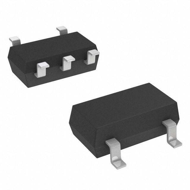
| 产品图片 |
|
| rohs | 符合RoHS无铅 / 符合限制有害物质指令(RoHS)规范要求 |
| 产品系列 | 放大器 IC,运算放大器 - 运放,Texas Instruments LPV324MX/NOPB- |
| 数据手册 | |
| 产品型号 | LPV324MX/NOPB |
| 产品种类 | 运算放大器 - 运放 |
| 供应商器件封装 | 14-SOICN |
| 共模抑制比—最小值 | 50 dB |
| 关闭 | No Shutdown |
| 其它名称 | LPV324MX/NOPBCT |
| 包装 | 剪切带 (CT) |
| 压摆率 | 0.1 V/µs |
| 商标 | Texas Instruments |
| 增益带宽生成 | 0.152 MHz |
| 增益带宽积 | 152kHz |
| 安装类型 | 表面贴装 |
| 安装风格 | SMD/SMT |
| 封装 | Reel |
| 封装/外壳 | 14-SOIC(0.154",3.90mm 宽) |
| 封装/箱体 | SOIC-14 |
| 工作温度 | -40°C ~ 85°C |
| 工作电源电压 | 2.7 V to 5 V |
| 工厂包装数量 | 2500 |
| 放大器类型 | 通用 |
| 最大工作温度 | + 85 C |
| 最小工作温度 | - 40 C |
| 标准包装 | 1 |
| 电压-电源,单/双 (±) | 2.7 V ~ 5 V |
| 电压-输入失调 | 1.5mV |
| 电流-电源 | 28µA |
| 电流-输入偏置 | 2nA |
| 电流-输出/通道 | 16mA |
| 电源电流 | 28 uA |
| 电路数 | 4 |
| 系列 | LPV324-N |
| 转换速度 | 0.1 V/us |
| 输入偏压电流—最大 | 50 nA |
| 输入补偿电压 | 7 mV |
| 输出电流 | 2 mA |
| 输出类型 | 满摆幅 |
| 通道数量 | 4 Channel |


- 商务部:美国ITC正式对集成电路等产品启动337调查
- 曝三星4nm工艺存在良率问题 高通将骁龙8 Gen1或转产台积电
- 太阳诱电将投资9.5亿元在常州建新厂生产MLCC 预计2023年完工
- 英特尔发布欧洲新工厂建设计划 深化IDM 2.0 战略
- 台积电先进制程称霸业界 有大客户加持明年业绩稳了
- 达到5530亿美元!SIA预计今年全球半导体销售额将创下新高
- 英特尔拟将自动驾驶子公司Mobileye上市 估值或超500亿美元
- 三星加码芯片和SET,合并消费电子和移动部门,撤换高东真等 CEO
- 三星电子宣布重大人事变动 还合并消费电子和移动部门
- 海关总署:前11个月进口集成电路产品价值2.52万亿元 增长14.8%


PDF Datasheet 数据手册内容提取
Product Sample & Technical Tools & Support & Folder Buy Documents Software Community LPV321-N,LPV324-N,LPV358-N SNOS413E–AUGUST2000–REVISEDNOVEMBER2016 LPV321-N Single, LPV358-N Dual, and LPV324-N Quad General-Purpose, Low Voltage, Low Power, Rail-to-Rail Output Operational Amplifiers 1 Features 3 Description • Specified2.7-Vand5-VPerformance The LPV3xx-N are low power (9-µA per channel at 1 5V)versionsoftheLMV3xxopamps.Thisisanother • NoCrossoverDistortion additiontotheLMVfamilyofcommodityopamps. • Space-SavingPackage The LPV3xx-N are the most cost effective solutions – 5-PinSC702 × 2.1 ×1mm for the applications where low voltage, low power • IndustrialTemperatureRange:−40°Cto85°C operation, space saving and low price are needed. • Gain-BandwidthProduct:152kHz The LPV3xx-N have rail-to-rail output swing capability and the input common-mode voltage range includes • LowSupplyCurrent ground. They all exhibit excellent speed-power ratio, – LPV321-N:9 µA achieving 152 kHz of bandwidth with a supply current – LPV358-N:15µA ofonly9µA. – LPV324-N:28µA The LPV321-N is available in space saving 5-Pin • Rail-to-RailOutputSwingat100kΩLoad: SC70, which is approximately half the size of 5-Pin SOT-23. The small package saves space on PC – V+− 3.5mV boards, and enables the design of small portable – V− +90mV electronicdevices.Italsoallowsthedesignertoplace • V ,−0.2VtoV+−0.8V the device closer to the signal source to reduce noise CM pickupandincreasesignalintegrity. 2 Applications The chips are built with Texas Instruments's • ActiveFilters advanced submicron silicon-gate BiCMOS process. The LPV3xx-N have bipolar input and output stages • General-PurposeLowVoltageApplications for improved noise performance and higher output • General-PurposePortableDevices currentdrive. DeviceInformation(1) PARTNUMBER PACKAGE BODYSIZE(NOM) SC70(5) 2.00mm×1.25mm LPV321-N SOT-23(5) 2.90mm×1.60mm SOIC(8) 4.90mm×3.91mm LPV358-N VSSOP(8) 3.00mm×3.00mm SOIC(14) 8.65mm×3.91mm LPV324-N TSSOP(14) 5.00mm×4.40mm (1) For all available packages, see the orderable addendum at theendofthedatasheet. MicropowerSupplyCurrent Rail-to-RailOutputSwing 1 An IMPORTANT NOTICE at the end of this data sheet addresses availability, warranty, changes, use in safety-critical applications, intellectualpropertymattersandotherimportantdisclaimers.PRODUCTIONDATA.
LPV321-N,LPV324-N,LPV358-N SNOS413E–AUGUST2000–REVISEDNOVEMBER2016 www.ti.com Table of Contents 1 Features.................................................................. 1 7.4 DeviceFunctionalModes........................................14 2 Applications........................................................... 1 8 ApplicationandImplementation........................ 16 3 Description............................................................. 1 8.1 ApplicationInformation ..........................................16 4 RevisionHistory..................................................... 2 8.2 TypicalApplications................................................16 5 PinConfigurationandFunctions......................... 3 9 PowerSupplyRecommendations...................... 19 6 Specifications......................................................... 4 10 Layout................................................................... 20 6.1 AbsoluteMaximumRatings......................................4 10.1 LayoutGuidelines.................................................20 6.2 ESDRatings..............................................................4 10.2 LayoutExample....................................................20 6.3 RecommendedOperatingConditions.......................4 11 DeviceandDocumentationSupport................. 21 6.4 ThermalInformation..................................................4 11.1 DeviceSupport ....................................................21 6.5 DCElectricalCharacteristics–2.7V........................5 11.2 DocumentationSupport .......................................21 6.6 ACElectricalCharacteristics–2.7V........................5 11.3 RelatedLinks........................................................21 6.7 DCElectricalCharacteristics–5V...........................5 11.4 ReceivingNotificationofDocumentationUpdates21 6.8 ACElectricalCharacteristics–5V...........................6 11.5 CommunityResources..........................................21 6.9 TypicalCharacteristics..............................................7 11.6 Trademarks...........................................................21 7 DetailedDescription............................................ 13 11.7 ElectrostaticDischargeCaution............................22 7.1 Overview ................................................................13 11.8 Glossary................................................................22 7.2 FunctionalBlockDiagram.......................................13 12 Mechanical,Packaging,andOrderable Information........................................................... 22 7.3 FeatureDescription.................................................13 4 Revision History NOTE:Pagenumbersforpreviousrevisionsmaydifferfrompagenumbersinthecurrentversion. ChangesfromRevisionD(March2013)toRevisionE Page • AddedESDRatingstable,FeatureDescriptionsection,DeviceFunctionalModes,ApplicationandImplementation section,PowerSupplyRecommendationssection,Layoutsection,DeviceandDocumentationSupportsection,and Mechanical,Packaging,andOrderableInformationsection.................................................................................................. 1 • DeletedSolderingtemperature(235°Cmaximum)................................................................................................................. 4 • ChangedThermalResistance,R ,valuesFrom:478To:296.7(SC70),From:265To:206.6(SOT-23),From:190 θJA To:130.1(8-PinSOIC),From:235To:187.5(VSSOP),From:145To:103.9(14-PinSOIC),From:155To:132.7 (TSSOP)................................................................................................................................................................................. 4 ChangesfromRevisionC(March2013)toRevisionD Page • ChangedlayoutofNationalSemiconductorDataSheettoTIformat.................................................................................... 1 2 SubmitDocumentationFeedback Copyright©2000–2016,TexasInstrumentsIncorporated ProductFolderLinks:LPV321-N LPV324-N LPV358-N
LPV321-N,LPV324-N,LPV358-N www.ti.com SNOS413E–AUGUST2000–REVISEDNOVEMBER2016 5 Pin Configuration and Functions DBVorDCKPackage DorDGKPackage DorPWPackage 5-PinSC70orSOT-23 8-PinSOICorVSSOP 14-PinSOICorTSSOP TopView TopView TopView IN+ 1 5 V+ OUT A 1 8 V+ OUT A 1 14 OUT D V- 2 -IN A 2 7 OUT B -IN A 2 13 -IN D IN- 3 4 OUT +IN A 3 6 -IN B +IN A 3 12 +IN D V- 4 5 +IN B V+ 4 11 V- +IN B 5 10 +IN C -IN B 6 9 -IN C OUT B 7 8 OUT C PinFunctions PIN SC70or SOICor SOICor TYPE(1) DESCRIPTION NAME SOT-23 VSSOP TSSOP +IN 1 — — I Noninvertinginput INA+ — 3 3 I Noninvertinginput,channelA INB+ — 5 5 I Noninvertinginput,channelB INC+ — — 10 I Noninvertinginput,channelC IND+ — — 12 I Noninvertinginput,channelD –IN 3 — — I Invertinginput INA– — 2 2 I Invertinginput,channelA INB– — 6 6 I Invertinginput,channelB INC– — — 9 I Invertinginput,channelC IND– — — 13 I Invertinginput,channelD OUTPUT 4 — — O Output OUTA — 1 1 O Output,channelA OUTB — 7 7 O Output,channelB OUTC — — 8 O Output,channelC OUTD — — 14 O Output,channelD V+ 5 8 4 P Positive(highest)powersupply V– 2 4 11 P Negative(lowest)powersupply (1) I=Input,O=Output,P=Power Copyright©2000–2016,TexasInstrumentsIncorporated SubmitDocumentationFeedback 3 ProductFolderLinks:LPV321-N LPV324-N LPV358-N
LPV321-N,LPV324-N,LPV358-N SNOS413E–AUGUST2000–REVISEDNOVEMBER2016 www.ti.com 6 Specifications 6.1 Absolute Maximum Ratings overoperatingfree-airtemperaturerange(unlessotherwisenoted)(1) MIN MAX UNIT Differentialinputvoltage ±Supplyvoltage Supplyvoltage(V+–V−) 5.5 V OutputshortcircuittoV+ See(2) OutputshortcircuittoV− See(3) Junctiontemperature,T (4) 150 °C J(MAX) Storagetemperature,T –65 150 °C stg (1) StressesbeyondthoselistedunderAbsoluteMaximumRatingsmaycausepermanentdamagetothedevice.Thesearestressratings only,whichdonotimplyfunctionaloperationofthedeviceattheseoranyotherconditionsbeyondthoseindicatedunderRecommended OperatingConditions.Exposuretoabsolute-maximum-ratedconditionsforextendedperiodsmayaffectdevicereliability. (2) ShortingoutputtoV+willadverselyaffectreliability. (3) ShortingoutputtoV−willadverselyaffectreliability. (4) ThemaximumpowerdissipationisafunctionofT andR .Themaximumallowablepowerdissipationatanyambient J(MAX) θJA temperatureisP =(T –T )/R .AllnumbersapplyforpackagessoldereddirectlyontoaPCB. D J(MAX) A θJA 6.2 ESD Ratings VALUE UNIT LPV321-NinDBVandDCKPackages Human-bodymodel(HBM),perANSI/ESDA/JEDECJS-001(1) ±1500 V Electrostaticdischarge V (ESD) Machinemodel ±100 LPV358-NinDandDGKPackages Human-bodymodel(HBM),perANSI/ESDA/JEDECJS-001(1) ±1500 V Electrostaticdischarge V (ESD) Machinemodel ±100 LPV324-NinDandPWPackages Human-bodymodel(HBM),perANSI/ESDA/JEDECJS-001(1) ±2000 V Electrostaticdischarge V (ESD) Machinemodel ±100 (1) HumanBodyModel,applicablestd.MIL-STD-883,Method3015.7.MachineModel,applicablestd.JESD22-A115-A(ESDMMstd.of JEDEC)Field-InducedCharge-DeviceModel,applicablestd.JESD22-C101-C(ESDFICDMstd.ofJEDEC). 6.3 Recommended Operating Conditions overoperatingfree-airtemperaturerange(unlessotherwisenoted) MIN MAX UNIT Supplyvoltage 2.7 5 V Operatingtemperature –40 85 °C 6.4 Thermal Information LPV321-N LPV358-N LPV324-N THERMALMETRIC(1) DBV DCK DGK D D PW UNIT (SOT-23) (SC70) (VSSOP) (SOIC) (SOIC) (TSSOP) 5PINS 5PINS 8PINS 8PINS 14PINS 14PINS R Junction-to-ambientthermalresistance 206.6 296.7 187.5 130.1 103.9 132.7 °C/W θJA R Junction-to-case(top)thermalresistance 167.2 128.1 77.7 74.3 61.6 59.1 °C/W θJC(top) R Junction-to-boardthermalresistance 65.5 74.3 108 70.7 58.4 75.1 °C/W θJB ψ Junction-to-topcharacterizationparameter 50.2 6.5 15.2 23.1 21.2 10.8 °C/W JT ψ Junction-to-boardcharacterizationparameter 65.1 73.6 106.5 70.2 58.1 74.58 °C/W JB R Junction-to-case(bottom)thermalresistance — — — — — — °C/W θJC(bot) (1) Formoreinformationabouttraditionalandnewthermalmetrics,seetheSemiconductorandICPackageThermalMetricsapplication report. 4 SubmitDocumentationFeedback Copyright©2000–2016,TexasInstrumentsIncorporated ProductFolderLinks:LPV321-N LPV324-N LPV358-N
LPV321-N,LPV324-N,LPV358-N www.ti.com SNOS413E–AUGUST2000–REVISEDNOVEMBER2016 6.5 DC Electrical Characteristics – 2.7 V T =25°C,V+=2.7V,V−=0V,V =1V,V =V+/2,andR >1MΩ(unlessotherwisenoted) J CM O L PARAMETER TESTCONDITIONS MIN(1) TYP(2) MAX(1) UNIT V Inputoffsetvoltage 1.2 7 mV OS TCV Inputoffsetvoltageaveragedrift 2 µV/°C OS I Inputbiascurrent 1.7 50 nA B I Inputoffsetcurrent 0.6 40 nA OS CMRR Commonmoderejectionratio 0V≤V ≤1.7V 50 70 dB CM PSRR Powersupplyrejectionratio 2.7V≤V+≤5V,V =1V,V =1V 50 65 dB O CM 0 −0.2 V Inputcommon-modevoltage ForCMRR≥50dB V CM 1.9 1.7 V+−100 V+−3 V Outputswing R =100kΩto1.35V mV O L 80 180 LPV321-N 4 8 I Supplycurrent LPV358-N,bothamplifiers 8 16 µA S LPV324-N,allfouramplifiers 16 24 (1) Alllimitsarespecifiedbytestingorstatisticalanalysis. (2) Typicalvaluesrepresentthemostlikelyparametricnormasdeterminedatthetimeofcharacterization.Actualtypicalvaluesmayvary overtimeandwillalsodependontheapplicationandconfiguration.Thetypicalvaluesarenottestedandarenotensuredonshipped productionmaterial. 6.6 AC Electrical Characteristics – 2.7 V T =25°C,V+=2.7V,V−=0V,V =1V,V =V+/2,andR >1MΩ(unlessotherwisenoted) J CM O L PARAMETER TESTCONDITIONS MIN(1) TYP(2) MAX(1) UNIT GBWP Gain-bandwidthproduct C =22pF 112 kHz L Φ Phasemargin 97 ° m G Gainmargin 35 dB m e Input-referredvoltagenoise f=1kHz 178 nV/√Hz n i Input-referredcurrentnoise f=1kHz 0.5 pA/√Hz n (1) Alllimitsarespecifiedbytestingorstatisticalanalysis. (2) Typicalvaluesrepresentthemostlikelyparametricnormasdeterminedatthetimeofcharacterization.Actualtypicalvaluesmayvary overtimeandwillalsodependontheapplicationandconfiguration.Thetypicalvaluesarenottestedandarenotensuredonshipped productionmaterial. 6.7 DC Electrical Characteristics – 5 V T =25°C,V+=5V,V−=0V,V =2V,V =V+/2,andR >1MΩ(unlessotherwisenoted) J CM O L PARAMETER TESTCONDITIONS MIN(1) TYP(2) MAX(1) UNIT T =25°C 1.5 7 J V Inputoffsetvoltage mV OS T =–40°Cto85°C 10 J Inputoffsetvoltageaverage TCV 2 µV/°C OS drift T =25°C 2 50 J I Inputbiascurrent nA B T =–40°Cto85°C 60 J T =25°C 0.6 40 J I Inputoffsetcurrent nA OS T =–40°Cto85°C 50 J Commonmoderejection CMRR 0V≤V ≤4V 50 71 dB ratio CM PSRR Powersupplyrejectionratio 2.7V≤V+≤5V,V =1V,V =1V 50 65 dB O CM (1) Alllimitsarespecifiedbytestingorstatisticalanalysis. (2) Typicalvaluesrepresentthemostlikelyparametricnormasdeterminedatthetimeofcharacterization.Actualtypicalvaluesmayvary overtimeandwillalsodependontheapplicationandconfiguration.Thetypicalvaluesarenottestedandarenotensuredonshipped productionmaterial. Copyright©2000–2016,TexasInstrumentsIncorporated SubmitDocumentationFeedback 5 ProductFolderLinks:LPV321-N LPV324-N LPV358-N
LPV321-N,LPV324-N,LPV358-N SNOS413E–AUGUST2000–REVISEDNOVEMBER2016 www.ti.com DC Electrical Characteristics – 5 V (continued) T =25°C,V+=5V,V−=0V,V =2V,V =V+/2,andR >1MΩ(unlessotherwisenoted) J CM O L PARAMETER TESTCONDITIONS MIN(1) TYP(2) MAX(1) UNIT 0 −0.2 V Inputcommon-modevoltage ForCMRR≥50dB V CM 4.2 4 T =25°C 15 100 A Largesignalvoltagegain(3) R =100kΩ J V/mV V L T =–40°Cto85°C 10 J Sourcing TJ=25°C V+−100 V+−3.5 RL=100kΩto2.5V TJ=–40°Cto85°C V+−200 V Outputswing mV O Sinking TJ=25°C 90 180 RL=100kΩto2.5V TJ=–40°Cto85°C 220 Outputshortcircuitcurrent LPV3xx-N,V =0V 2 16 sourcing O I mA O Outputshortcircuitcurrent LPV321-N,VO=5V 20 60 sinking LPV324-NandLPV358-N,V =5V 11 16 O T =25°C 9 12 J LPV321-N T =–40°Cto85°C 15 J LPV358-N, TJ=25°C 15 20 I Supplycurrent µA S Bothamplifiers T =–40°Cto85°C 24 J LPV324-N, TJ=25°C 28 42 Allfouramplifiers T =–40°Cto85°C 46 J (3) R isconnectedtoV-.Theoutputvoltageis0.5V≤V ≤4.5V. L O 6.8 AC Electrical Characteristics – 5 V T =25°C,V+=5V,V−=0V,V =2V,V =V+/2,andR >1MΩ(unlessotherwisenoted) J CM O L PARAMETER TESTCONDITIONS MIN(1) TYP(2) MAX(1) UNIT SR Slewrate(3) 0.1 V/µs GBWP Gain-bandwidthproduct C =22pF 152 kHz L Φ Phasemargin 87 ° m G Gainmargin 19 dB m e Input-referredvoltagenoise f=1kHz 146 nV/√Hz n i Input-referredcurrentnoise f=1kHz 0.3 pA/√Hz n (1) Alllimitsarespecifiedbytestingorstatisticalanalysis. (2) Typicalvaluesrepresentthemostlikelyparametricnormasdeterminedatthetimeofcharacterization.Actualtypicalvaluesmayvary overtimeandwillalsodependontheapplicationandconfiguration.Thetypicalvaluesarenottestedandarenotensuredonshipped productionmaterial. (3) Connectedasvoltagefollowerwith3Vstepinput.Numberspecifiedistheslowerofthepositiveandnegativeslewrates. 6 SubmitDocumentationFeedback Copyright©2000–2016,TexasInstrumentsIncorporated ProductFolderLinks:LPV321-N LPV324-N LPV358-N
LPV321-N,LPV324-N,LPV358-N www.ti.com SNOS413E–AUGUST2000–REVISEDNOVEMBER2016 6.9 Typical Characteristics V =5V,singlesupply,andT =25°C(unlessotherwisenoted) S A Figure1.SupplyCurrentvsSupplyVoltage(LPV321-N) Figure2.InputCurrentvsTemperature Figure3.SourcingCurrentvsOutputVoltage Figure4.SourcingCurrentvsOutputVoltage Figure5.SinkingCurrentvsOutputVoltage Figure6.SinkingCurrentvsOutputVoltage Copyright©2000–2016,TexasInstrumentsIncorporated SubmitDocumentationFeedback 7 ProductFolderLinks:LPV321-N LPV324-N LPV358-N
LPV321-N,LPV324-N,LPV358-N SNOS413E–AUGUST2000–REVISEDNOVEMBER2016 www.ti.com Typical Characteristics (continued) V =5V,singlesupply,andT =25°C(unlessotherwisenoted) S A Figure7.OutputVoltageSwingvsSupplyVoltage Figure8.InputVoltageNoisevsFrequency Figure9.InputCurrentNoisevsFrequency Figure10.InputCurrentNoisevsFrequency Figure11.CrosstalkRejectionvsFrequency Figure12.PSRRvsFrequency 8 SubmitDocumentationFeedback Copyright©2000–2016,TexasInstrumentsIncorporated ProductFolderLinks:LPV321-N LPV324-N LPV358-N
LPV321-N,LPV324-N,LPV358-N www.ti.com SNOS413E–AUGUST2000–REVISEDNOVEMBER2016 Typical Characteristics (continued) V =5V,singlesupply,andT =25°C(unlessotherwisenoted) S A Figure13.CMRRvsFrequency Figure14.CMRRvsInputCommonModeVoltage Figure15.CMRRvsInputCommonModeVoltage Figure16.ΔV vsV OS CM Figure17.ΔV vsV Figure18.InputVoltagevsOutputVoltage OS CM Copyright©2000–2016,TexasInstrumentsIncorporated SubmitDocumentationFeedback 9 ProductFolderLinks:LPV321-N LPV324-N LPV358-N
LPV321-N,LPV324-N,LPV358-N SNOS413E–AUGUST2000–REVISEDNOVEMBER2016 www.ti.com Typical Characteristics (continued) V =5V,singlesupply,andT =25°C(unlessotherwisenoted) S A Figure19.InputVoltagevsOutputVoltage Figure20.Open-LoopFrequencyResponse Figure21.Open-LoopFrequencyResponse Figure22.GainandPhasevsCapacitiveLoad Figure23.GainandPhasevsCapacitiveLoad Figure24.SlewRatevsSupplyVoltage 10 SubmitDocumentationFeedback Copyright©2000–2016,TexasInstrumentsIncorporated ProductFolderLinks:LPV321-N LPV324-N LPV358-N
LPV321-N,LPV324-N,LPV358-N www.ti.com SNOS413E–AUGUST2000–REVISEDNOVEMBER2016 Typical Characteristics (continued) V =5V,singlesupply,andT =25°C(unlessotherwisenoted) S A Figure25.NoninvertingLargeSignalPulseResponse Figure26.NoninvertingSmallSignalPulseResponse Figure27.InvertingLargeSignalPulseResponse Figure28.InvertingSmallSignalPulseResponse Figure29.StabilityvsCapacitiveLoad Figure30.StabilityvsCapacitiveLoad Copyright©2000–2016,TexasInstrumentsIncorporated SubmitDocumentationFeedback 11 ProductFolderLinks:LPV321-N LPV324-N LPV358-N
LPV321-N,LPV324-N,LPV358-N SNOS413E–AUGUST2000–REVISEDNOVEMBER2016 www.ti.com Typical Characteristics (continued) V =5V,singlesupply,andT =25°C(unlessotherwisenoted) S A Figure31.StabilityvsCapacitiveLoad Figure32.StabilityvsCapacitiveLoad Figure33.THDvsFrequency Figure34.Open-LoopOutputImpedancevsFrequency Figure35.ShortCircuitCurrentvsTemperature(Sinking) Figure36.ShortCircuitCurrentvsTemperature(Sourcing) 12 SubmitDocumentationFeedback Copyright©2000–2016,TexasInstrumentsIncorporated ProductFolderLinks:LPV321-N LPV324-N LPV358-N
LPV321-N,LPV324-N,LPV358-N www.ti.com SNOS413E–AUGUST2000–REVISEDNOVEMBER2016 7 Detailed Description 7.1 Overview The LPV321-N, LPV358-N, and LPV324-N devices are micropower (10-µA) versions of the popular LMV3xx-N. The LPV321-N is the single-channel version. The LPV358-N is the dual, and the LPV324-N is the quad. The LPV32x-Narethemostcosteffectivesolutionforapplicationswherelowpowerandlowvoltageoperation,space efficiency, and low-price are important. The LPV3x-N have rail-to-rail output swing capability and the input common-mode voltage range includes ground. They all exhibit excellent speed to power ratio, achieving 152 kHz ofbandwidthand0.1-V/µsslewratewith10mAofsupplycurrent. 7.2 Functional Block Diagram + V IN– _ OUT + IN + – V Copyright © 2016, Texas Instruments Incorporated 7.3 Feature Description 7.3.1 Size The small footprints of the LPV3xx-N packages save space on printed circuit boards, and enable the design of smaller electronic products (such as cellular phones, pagers, or other portable systems). The low profile of the LPV3xx-NmakethempossibletouseinPCMCIAtypeIIIcards. 7.3.2 SignalIntegrity Signals can pick up noise between the signal source and the amplifier. By using a physically smaller amplifier package, the LPV3xx-N can be placed closer to the signal source, reducing noise pickup and increasing signal integrity. 7.3.3 SimplifiedBoardLayout These products help avoid using long printed-circuit traces in the PCB. This means no additional components, such as capacitors and resistors, are needed to filter out unwanted signals due to the interference between the longprinted-circuittraces. 7.3.4 LowSupplyCurrent Thesedeviceshelpmaximizebatterylife.Theyareidealforbatterypoweredsystems. 7.3.5 LowSupplyVoltage TI provides ensured performance at 2.7 V and 5 V. These specifications ensure operation throughout the battery lifetime. 7.3.6 Rail-to-RailOutput Rail-to-rail output swing provides maximum possible dynamic range at the output. This is particularly important whenoperatingonlow-supplyvoltages. Copyright©2000–2016,TexasInstrumentsIncorporated SubmitDocumentationFeedback 13 ProductFolderLinks:LPV321-N LPV324-N LPV358-N
LPV321-N,LPV324-N,LPV358-N SNOS413E–AUGUST2000–REVISEDNOVEMBER2016 www.ti.com Feature Description (continued) 7.3.7 InputIncludesGround AllowsdirectsensingnearGNDinsinglesupplyoperation. The differential input voltage may be larger than V+ without damaging the device. Protection should be provided to prevent the input voltages from going negative more than −0.3 V (at 25°C). An input clamp diode with a resistortotheICinputterminalcanbeused. 7.4 Device Functional Modes The LPV3xx-N can be operated as a single-supply or a dual-supply operational amplifier depending on the application. 7.4.1 CapacitiveLoadTolerance The LPV3xx-N can directly drive 200 pF in unity-gain without oscillation. The unity-gain follower is the most sensitive configuration to capacitive loading. Direct capacitive loading reduces the phase margin of amplifiers. The combination of the amplifier's output impedance and the capacitive load induces phase lag. This results in either an underdamped pulse response or oscillation. To drive a heavier capacitive load, circuit in Figure 37 can beused. Figure37. IndirectlyDrivingACapacitiveLoadUsingResistiveIsolation In Figure 37, the isolation resistor (R ) and the load capacitor (C ) form a pole to increase stability by adding ISO L morephasemargintotheoverallsystem.ThedesiredperformancedependsonthevalueofR .Thebiggerthe ISO R resistor value, the more stable V is. Figure 38 is an output waveform of Figure 37 using 100 kΩ for R ISO OUT ISO and1000pFforC . L Figure38. PulseResponseoftheLPV324CircuitinFigure37 14 SubmitDocumentationFeedback Copyright©2000–2016,TexasInstrumentsIncorporated ProductFolderLinks:LPV321-N LPV324-N LPV358-N
LPV321-N,LPV324-N,LPV358-N www.ti.com SNOS413E–AUGUST2000–REVISEDNOVEMBER2016 Device Functional Modes (continued) The circuit in Figure 39 is an improvement to the one in Figure 37 because it provides DC accuracy as well as AC stability. If there were a load resistor in Figure 37, the output would be voltage divided by R and the load ISO resistor. Instead, in Figure 39, R provides the DC accuracy by using feed-forward techniques to connect V to F IN R . Caution is needed in choosing the value of R due to the input bias current of the LPV3xx-N. C and R L F F ISO serve to counteract the loss of phase margin by feeding the high frequency component of the output signal back to the amplifier's inverting input, thereby preserving phase margin in the overall feedback loop. Increased capacitivedriveispossiblebyincreasingthevalueofC .Thisinturnslowsdownthepulseresponse. F Figure39. IndirectlyDrivingACapacitiveLoadWithDCAccuracy 7.4.2 InputBiasCurrentCancellation The LPV3xx-N family has a bipolar input stage. The typical input bias current of LPV3xx-N is 1.5 nA with 5-V supply. Thus a 100-kΩ input resistor causes 0.15 mV of error voltage. By balancing the resistor values at both inverting and noninverting inputs, the error caused by the amplifier's input bias current is reduced. The circuit in Figure40showshowtocanceltheerrorcausedbyinputbiascurrent. Figure40. CancellingtheErrorCausedbyInputBiasCurrent Copyright©2000–2016,TexasInstrumentsIncorporated SubmitDocumentationFeedback 15 ProductFolderLinks:LPV321-N LPV324-N LPV358-N
LPV321-N,LPV324-N,LPV358-N SNOS413E–AUGUST2000–REVISEDNOVEMBER2016 www.ti.com 8 Application and Implementation NOTE Information in the following applications sections is not part of the TI component specification, and TI does not warrant its accuracy or completeness. TI’s customers are responsible for determining suitability of components for their purposes. Customers should validateandtesttheirdesignimplementationtoconfirmsystemfunctionality. 8.1 Application Information The LPV3xx-N family of amplifiers is specified for operation from 2.7 V to 5 V (±1.35 V to ±2.5 V). Many of the specificationsapplyfrom –40°Cto125°C.Theyprovideground-sensinginputsaswellasrail-to-railoutputswing. Parameters that can exhibit significant variance with regard to operating voltage or temperature are presented in theTypicalCharacteristics. 8.2 Typical Applications 8.2.1 SimpleLow-PassActiveFilter Asimplelow-passfilterisshowninFigure41. Figure41. SimpleLow-PassActiveFilterSchematic 8.2.1.1 DesignRequirements The low-pass filter is shown in Figure 41 passes low frequencies and attenuate frequencies above corner frequency(fc)ataroll-offrateof20dB/Decade. 8.2.1.2 DetailedDesignProcedure The low-frequency gain (ω → o) is defined by −R /R . This allows low-frequency gains other than unity to be 3 1 obtained. The filter has a −20 dB/decade roll-off after its corner frequency fc. R must be chosen equal to the 2 parallel combination of R and R to minimize errors due to bais current. The frequency response of the filter is 1 3 showninFigure42. R A (cid:16) 3 L R 1 1 f c 2SR C 3 1 R R IIR 2 1 3 (1) 16 SubmitDocumentationFeedback Copyright©2000–2016,TexasInstrumentsIncorporated ProductFolderLinks:LPV321-N LPV324-N LPV358-N
LPV321-N,LPV324-N,LPV358-N www.ti.com SNOS413E–AUGUST2000–REVISEDNOVEMBER2016 Typical Applications (continued) Note that the single op amp active filters are used in to the applications that require low quality factor, Q (≤ 10), low frequency (≤ 5 kHz), and low gain (≤ 10), or a small value for the product of gain times Q (≤ 100). The op amp must have an open loop voltage gain at the highest frequency of interest at least 50 times larger than the gain of the filter at this frequency. In addition, the selected op amp must have a slew rate that meets the requirementsinEquation2. SlewRate≥0.5×(ω V )×10−6V/µsec H OPP where • ω isthehighestfrequencyofinterest H • V istheoutputpeak-to-peakvoltage (2) OPP 8.2.1.3 ApplicationCurve Figure42. FrequencyResponseofSimpleLow-passActiveFilter 8.2.2 DifferenceAmplifier The difference amplifier allows the subtraction of two voltages or, as a special case, the cancellation of a signal commontotwoinputs.Itisusefulasacomputationalamplifierinmakingadifferentialtosingle-endedconversion orinrejectingacommonmodesignal. Figure43. DifferenceAmplifierSchematic §R1(cid:14)R2•R4 R2 §R1(cid:14)R2•R3 V(cid:14) VOUT ¤ ‚ V2(cid:16) V1(cid:14)¤ ‚ u 'R3(cid:14)R4„R1 R1 'R3(cid:14)R4„R1 2 for R1 R3andR2 R4 R2 V(cid:14) V (cid:11)V (cid:16)V1(cid:12) (cid:14) OUT 2 R1 2 (3) 8.2.3 InstrumentationCircuits The input impedance of the previous difference amplifier is set by the resistor R , R , R , and R . To eliminate 1 2 3 4 the problems of low input impedance, one way is to use a voltage follower ahead of each input as shown in the followingtwoinstrumentationamplifiers. Copyright©2000–2016,TexasInstrumentsIncorporated SubmitDocumentationFeedback 17 ProductFolderLinks:LPV321-N LPV324-N LPV358-N
LPV321-N,LPV324-N,LPV358-N SNOS413E–AUGUST2000–REVISEDNOVEMBER2016 www.ti.com Typical Applications (continued) 8.2.3.1 ThreeOperatingAmplifierInstrumentation ThequadLPV324canbeusedtobuildathree-op-ampinstrumentationamplifierasshowninFigure44 Figure44. Three-op-ampInstrumentationAmplifierSchematic The first stage of this instrumentation amplifier is a differential-input, differential-output amplifier, with two voltage followers. These two voltage followers assure that the input impedance is over 100 MΩ. The gain of this instrumentation amplifier is set by the ratio of R /R . R should equal R and R equal R . Matching of R to R 2 1 3 1 4 2 3 1 and R to R affects the CMRR. For good CMRR over temperature, low drift resistors should be used. Making R 4 2 4 Slightly smaller than R and adding a trim pot equal to twice the difference between R and R will allow the 2 2 4 CMRRtobeadjustedforoptimum. 8.2.3.2 TwoOperatingAmplifierInstrumentation A two-op-amp instrumentation amplifier can also be used to make a high-input-impedance DC differential amplifier (Figure 45). As in the three-op-amp circuit, this instrumentation amplifier requires precise resistor matchingforgoodCMRR.R shouldequaltoR andR mustequalR . 4 1 3 2 Figure45. Two-op-ampInstrumentationAmplifierSchematic § R4• VO ¤1(cid:14) ‚(cid:11)V2(cid:16)V1(cid:12),whereR1 R4andR2 R3 ' R3„ Asshown:V 2(cid:11)V (cid:16)V (cid:12) O 2 1 (4) 8.2.3.3 Single-SupplyInvertingAmplifier There may be cases where the input signal going into the amplifier is negative. Because the amplifier is operating in single supply voltage, a voltage divider using R and R is implemented to bias the amplifier so the 3 4 input signal is within the input common-common voltage range of the amplifier. The capacitor C is placed 1 between the inverting input and resistor R to block the DC signal going into the AC signal source, V . The 1 IN valuesofR andC affectthecutofffrequencyinEquation5. 1 1 fc=1/2πR C (5) 1 1 18 SubmitDocumentationFeedback Copyright©2000–2016,TexasInstrumentsIncorporated ProductFolderLinks:LPV321-N LPV324-N LPV358-N
LPV321-N,LPV324-N,LPV358-N www.ti.com SNOS413E–AUGUST2000–REVISEDNOVEMBER2016 Typical Applications (continued) As a result, the output signal is centered around mid-supply (if the voltage divider provides V+/2 at the non- invertinginput).Theoutputcanswingtobothrails,maximizingthesignal-to-noiseratioinalowvoltagesystem. Figure46. Single-SupplyInvertingAmplifier R2 V (cid:16) V OUT IN R1 (6) 9 Power Supply Recommendations The LPV3xx-N is specified for operation from 2.7 V to 5.5 V; many specifications apply from –40°C to 125°C. Parameters that can exhibit significant variance with regard to operating voltage or temperature are presented in theTypicalCharacteristics. Place 0.1-µF bypass capacitors close to the power-supply pins to reduce errors coupling in from noisy or high impedance power supplies. For more detailed information on bypass capacitor placement, see Layout Guidelines section. Copyright©2000–2016,TexasInstrumentsIncorporated SubmitDocumentationFeedback 19 ProductFolderLinks:LPV321-N LPV324-N LPV358-N
LPV321-N,LPV324-N,LPV358-N SNOS413E–AUGUST2000–REVISEDNOVEMBER2016 www.ti.com 10 Layout 10.1 Layout Guidelines Forbestoperationalperformance,usegoodPCBlayoutpracticesincluding: • Noise can propagate into analog circuitry through the power pins of the circuit as a whole and the operational amplifier. Bypass capacitors are used to reduce the coupled noise by providing low impedance power sourceslocaltotheanalogcircuitry. • Connect low-ESR, 0.1-µF ceramic bypass capacitors between each supply pin and ground, placed as close to the device as possible. A single bypass capacitor from V+ to ground is applicable for single supply applications. • Separate grounding for analog and digital portions of circuitry is one of the simplest and most-effective methods of noise suppression. One or more layers on multilayer PCBs are usually devoted to ground planes. A ground plane helps distribute heat and reduces EMI noise pickup. Make sure to physically separate digital and analog grounds, paying attention to the flow of the ground current. For more detailed information, see CircuitBoardLayoutTechniques (SLOA089). • To reduce parasitic coupling, run the input traces as far away from the supply or output traces as possible. If it is not possible to keep them separate, it is much better to cross the sensitive trace perpendicular as opposedtoinparallelwiththenoisytrace. • Place the external components as close to the device as possible. Keeping RF and RG close to the inverting inputminimizesparasiticcapacitance,asshowninFigure47. • Keep the length of input traces as short as possible. Always remember that the input traces are the most sensitivepartofthecircuit. • Consider a driven, low-impedance guard ring around the critical traces. A guard ring can significantly reduce leakagecurrentsfromnearbytracesthatareatdifferentpotentials. 10.2 Layout Example Figure47. OperationalAmplifierBoardLayoutforNoninvertingConfiguration 20 SubmitDocumentationFeedback Copyright©2000–2016,TexasInstrumentsIncorporated ProductFolderLinks:LPV321-N LPV324-N LPV358-N
LPV321-N,LPV324-N,LPV358-N www.ti.com SNOS413E–AUGUST2000–REVISEDNOVEMBER2016 11 Device and Documentation Support 11.1 Device Support 11.1.1 DevelopmentSupport • LPV321-NPSPICEModel (SNOM026) • LPV358-NPSPICEModel (SNOM022) • LPV324-NPSPICEModel (SNOM027) • TINA-TISPICE-BasedAnalogSimulationProgram • DIPAdapterEvaluationModule • TIUniversalOperationalAmplifierEvaluationModule • TIFilterproSoftware 11.2 Documentation Support 11.2.1 RelatedDocumentation Forrelateddocumentationseethefollowing: • HandbookofOperationalAmplifierApplications (SBOA092) • CompensateTransimpedanceAmplifiersIntuitively (SBOA055) • CircuitBoardLayoutTechniques (SLOA089) • AN-1803DesignConsiderationsforaTransimpedanceAmplifier(SNOA515) 11.3 Related Links The table below lists quick access links. Categories include technical documents, support and community resources,toolsandsoftware,andquickaccesstosampleorbuy. Table1.RelatedLinks TECHNICAL TOOLS& SUPPORT& PARTS PRODUCTFOLDER SAMPLE&BUY DOCUMENTS SOFTWARE COMMUNITY LPV321-N Clickhere Clickhere Clickhere Clickhere Clickhere LPV324-N Clickhere Clickhere Clickhere Clickhere Clickhere LPV358-N Clickhere Clickhere Clickhere Clickhere Clickhere 11.4 Receiving Notification of Documentation Updates To receive notification of documentation updates, navigate to the device product folder on ti.com. In the upper right corner, click on Alert me to register and receive a weekly digest of any product information that has changed.Forchangedetails,reviewtherevisionhistoryincludedinanyreviseddocument. 11.5 Community Resources The following links connect to TI community resources. Linked contents are provided "AS IS" by the respective contributors. They do not constitute TI specifications and do not necessarily reflect TI's views; see TI's Terms of Use. TIE2E™OnlineCommunity TI'sEngineer-to-Engineer(E2E)Community.Createdtofostercollaboration amongengineers.Ate2e.ti.com,youcanaskquestions,shareknowledge,exploreideasandhelp solveproblemswithfellowengineers. DesignSupport TI'sDesignSupport QuicklyfindhelpfulE2Eforumsalongwithdesignsupporttoolsand contactinformationfortechnicalsupport. 11.6 Trademarks E2EisatrademarkofTexasInstruments. Allothertrademarksarethepropertyoftheirrespectiveowners. Copyright©2000–2016,TexasInstrumentsIncorporated SubmitDocumentationFeedback 21 ProductFolderLinks:LPV321-N LPV324-N LPV358-N
LPV321-N,LPV324-N,LPV358-N SNOS413E–AUGUST2000–REVISEDNOVEMBER2016 www.ti.com 11.7 Electrostatic Discharge Caution Thesedeviceshavelimitedbuilt-inESDprotection.Theleadsshouldbeshortedtogetherorthedeviceplacedinconductivefoam duringstorageorhandlingtopreventelectrostaticdamagetotheMOSgates. 11.8 Glossary SLYZ022—TIGlossary. Thisglossarylistsandexplainsterms,acronyms,anddefinitions. 12 Mechanical, Packaging, and Orderable Information The following pages include mechanical, packaging, and orderable information. This information is the most current data available for the designated devices. This data is subject to change without notice and revision of thisdocument.Forbrowser-basedversionsofthisdatasheet,refertotheleft-handnavigation. 22 SubmitDocumentationFeedback Copyright©2000–2016,TexasInstrumentsIncorporated ProductFolderLinks:LPV321-N LPV324-N LPV358-N
PACKAGE OPTION ADDENDUM www.ti.com 6-Feb-2020 PACKAGING INFORMATION Orderable Device Status Package Type Package Pins Package Eco Plan Lead/Ball Finish MSL Peak Temp Op Temp (°C) Device Marking Samples (1) Drawing Qty (2) (6) (3) (4/5) LPV321M5/NOPB ACTIVE SOT-23 DBV 5 1000 Green (RoHS SN Level-1-260C-UNLIM -40 to 85 A27A & no Sb/Br) LPV321M5X/NOPB ACTIVE SOT-23 DBV 5 3000 Green (RoHS SN Level-1-260C-UNLIM -40 to 85 A27A & no Sb/Br) LPV321M7 NRND SC70 DCK 5 1000 TBD Call TI Call TI -40 to 85 A19 LPV321M7/NOPB ACTIVE SC70 DCK 5 1000 Green (RoHS SN Level-1-260C-UNLIM -40 to 85 A19 & no Sb/Br) LPV321M7X/NOPB ACTIVE SC70 DCK 5 3000 Green (RoHS SN Level-1-260C-UNLIM -40 to 85 A19 & no Sb/Br) LPV324M/NOPB ACTIVE SOIC D 14 55 Green (RoHS SN Level-1-260C-UNLIM -40 to 85 LPV324M & no Sb/Br) LPV324MT/NOPB ACTIVE TSSOP PW 14 94 Green (RoHS SN Level-1-260C-UNLIM -40 to 85 LPV324 & no Sb/Br) MT LPV324MTX NRND TSSOP PW 14 2500 TBD Call TI Call TI -40 to 85 LPV324 MT LPV324MTX/NOPB ACTIVE TSSOP PW 14 2500 Green (RoHS SN Level-1-260C-UNLIM -40 to 85 LPV324 & no Sb/Br) MT LPV324MX NRND SOIC D 14 2500 TBD Call TI Call TI -40 to 85 LPV324M LPV324MX/NOPB ACTIVE SOIC D 14 2500 Green (RoHS SN Level-1-260C-UNLIM -40 to 85 LPV324M & no Sb/Br) LPV358M/NOPB ACTIVE SOIC D 8 95 Green (RoHS SN Level-1-260C-UNLIM LPV & no Sb/Br) 358M LPV358MM/NOPB ACTIVE VSSOP DGK 8 1000 Green (RoHS SN Level-1-260C-UNLIM -40 to 85 P358 & no Sb/Br) LPV358MMX/NOPB ACTIVE VSSOP DGK 8 3500 Green (RoHS SN Level-1-260C-UNLIM -40 to 85 P358 & no Sb/Br) LPV358MX NRND SOIC D 8 2500 TBD Call TI Call TI -40 to 85 LPV 358M LPV358MX/NOPB ACTIVE SOIC D 8 2500 Green (RoHS SN Level-1-260C-UNLIM -40 to 85 LPV & no Sb/Br) 358M (1) The marketing status values are defined as follows: ACTIVE: Product device recommended for new designs. LIFEBUY: TI has announced that the device will be discontinued, and a lifetime-buy period is in effect. NRND: Not recommended for new designs. Device is in production to support existing customers, but TI does not recommend using this part in a new design. Addendum-Page 1
PACKAGE OPTION ADDENDUM www.ti.com 6-Feb-2020 PREVIEW: Device has been announced but is not in production. Samples may or may not be available. OBSOLETE: TI has discontinued the production of the device. (2) RoHS: TI defines "RoHS" to mean semiconductor products that are compliant with the current EU RoHS requirements for all 10 RoHS substances, including the requirement that RoHS substance do not exceed 0.1% by weight in homogeneous materials. Where designed to be soldered at high temperatures, "RoHS" products are suitable for use in specified lead-free processes. TI may reference these types of products as "Pb-Free". RoHS Exempt: TI defines "RoHS Exempt" to mean products that contain lead but are compliant with EU RoHS pursuant to a specific EU RoHS exemption. Green: TI defines "Green" to mean the content of Chlorine (Cl) and Bromine (Br) based flame retardants meet JS709B low halogen requirements of <=1000ppm threshold. Antimony trioxide based flame retardants must also meet the <=1000ppm threshold requirement. (3) MSL, Peak Temp. - The Moisture Sensitivity Level rating according to the JEDEC industry standard classifications, and peak solder temperature. (4) There may be additional marking, which relates to the logo, the lot trace code information, or the environmental category on the device. (5) Multiple Device Markings will be inside parentheses. Only one Device Marking contained in parentheses and separated by a "~" will appear on a device. If a line is indented then it is a continuation of the previous line and the two combined represent the entire Device Marking for that device. (6) Lead/Ball Finish - Orderable Devices may have multiple material finish options. Finish options are separated by a vertical ruled line. Lead/Ball Finish values may wrap to two lines if the finish value exceeds the maximum column width. Important Information and Disclaimer:The information provided on this page represents TI's knowledge and belief as of the date that it is provided. TI bases its knowledge and belief on information provided by third parties, and makes no representation or warranty as to the accuracy of such information. Efforts are underway to better integrate information from third parties. TI has taken and continues to take reasonable steps to provide representative and accurate information but may not have conducted destructive testing or chemical analysis on incoming materials and chemicals. TI and TI suppliers consider certain information to be proprietary, and thus CAS numbers and other limited information may not be available for release. In no event shall TI's liability arising out of such information exceed the total purchase price of the TI part(s) at issue in this document sold by TI to Customer on an annual basis. Addendum-Page 2
PACKAGE MATERIALS INFORMATION www.ti.com 29-Sep-2019 TAPE AND REEL INFORMATION *Alldimensionsarenominal Device Package Package Pins SPQ Reel Reel A0 B0 K0 P1 W Pin1 Type Drawing Diameter Width (mm) (mm) (mm) (mm) (mm) Quadrant (mm) W1(mm) LPV321M5/NOPB SOT-23 DBV 5 1000 178.0 8.4 3.2 3.2 1.4 4.0 8.0 Q3 LPV321M5X/NOPB SOT-23 DBV 5 3000 178.0 8.4 3.2 3.2 1.4 4.0 8.0 Q3 LPV321M7 SC70 DCK 5 1000 178.0 8.4 2.25 2.45 1.2 4.0 8.0 Q3 LPV321M7/NOPB SC70 DCK 5 1000 178.0 8.4 2.25 2.45 1.2 4.0 8.0 Q3 LPV321M7X/NOPB SC70 DCK 5 3000 178.0 8.4 2.25 2.45 1.2 4.0 8.0 Q3 LPV324MTX TSSOP PW 14 2500 330.0 12.4 6.95 5.6 1.6 8.0 12.0 Q1 LPV324MTX/NOPB TSSOP PW 14 2500 330.0 12.4 6.95 5.6 1.6 8.0 12.0 Q1 LPV324MX SOIC D 14 2500 330.0 16.4 6.5 9.35 2.3 8.0 16.0 Q1 LPV324MX/NOPB SOIC D 14 2500 330.0 16.4 6.5 9.35 2.3 8.0 16.0 Q1 LPV358MM/NOPB VSSOP DGK 8 1000 178.0 12.4 5.3 3.4 1.4 8.0 12.0 Q1 LPV358MMX/NOPB VSSOP DGK 8 3500 330.0 12.4 5.3 3.4 1.4 8.0 12.0 Q1 LPV358MX SOIC D 8 2500 330.0 12.4 6.5 5.4 2.0 8.0 12.0 Q1 LPV358MX/NOPB SOIC D 8 2500 330.0 12.4 6.5 5.4 2.0 8.0 12.0 Q1 PackMaterials-Page1
PACKAGE MATERIALS INFORMATION www.ti.com 29-Sep-2019 *Alldimensionsarenominal Device PackageType PackageDrawing Pins SPQ Length(mm) Width(mm) Height(mm) LPV321M5/NOPB SOT-23 DBV 5 1000 210.0 185.0 35.0 LPV321M5X/NOPB SOT-23 DBV 5 3000 210.0 185.0 35.0 LPV321M7 SC70 DCK 5 1000 210.0 185.0 35.0 LPV321M7/NOPB SC70 DCK 5 1000 210.0 185.0 35.0 LPV321M7X/NOPB SC70 DCK 5 3000 210.0 185.0 35.0 LPV324MTX TSSOP PW 14 2500 367.0 367.0 35.0 LPV324MTX/NOPB TSSOP PW 14 2500 367.0 367.0 35.0 LPV324MX SOIC D 14 2500 367.0 367.0 35.0 LPV324MX/NOPB SOIC D 14 2500 367.0 367.0 35.0 LPV358MM/NOPB VSSOP DGK 8 1000 210.0 185.0 35.0 LPV358MMX/NOPB VSSOP DGK 8 3500 367.0 367.0 35.0 LPV358MX SOIC D 8 2500 367.0 367.0 35.0 LPV358MX/NOPB SOIC D 8 2500 367.0 367.0 35.0 PackMaterials-Page2
PACKAGE OUTLINE DBV0005A SOT-23 - 1.45 mm max height SCALE 4.000 SMALL OUTLINE TRANSISTOR C 3.0 2.6 0.1 C 1.75 1.45 1.45 B A 0.90 PIN 1 INDEX AREA 1 5 2X 0.95 3.05 2.75 1.9 1.9 2 4 3 0.5 5X 0.3 0.15 0.2 C A B (1.1) TYP 0.00 0.25 GAGE PLANE 0.22 TYP 0.08 8 TYP 0.6 0 0.3 TYP SEATING PLANE 4214839/E 09/2019 NOTES: 1. All linear dimensions are in millimeters. Any dimensions in parenthesis are for reference only. Dimensioning and tolerancing per ASME Y14.5M. 2. This drawing is subject to change without notice. 3. Refernce JEDEC MO-178. 4. Body dimensions do not include mold flash, protrusions, or gate burrs. Mold flash, protrusions, or gate burrs shall not exceed 0.15 mm per side. www.ti.com
EXAMPLE BOARD LAYOUT DBV0005A SOT-23 - 1.45 mm max height SMALL OUTLINE TRANSISTOR PKG 5X (1.1) 1 5 5X (0.6) SYMM (1.9) 2 2X (0.95) 3 4 (R0.05) TYP (2.6) LAND PATTERN EXAMPLE EXPOSED METAL SHOWN SCALE:15X SOLDER MASK SOLDER MASK METAL UNDER METAL OPENING OPENING SOLDER MASK EXPOSED METAL EXPOSED METAL 0.07 MAX 0.07 MIN ARROUND ARROUND NON SOLDER MASK SOLDER MASK DEFINED DEFINED (PREFERRED) SOLDER MASK DETAILS 4214839/E 09/2019 NOTES: (continued) 5. Publication IPC-7351 may have alternate designs. 6. Solder mask tolerances between and around signal pads can vary based on board fabrication site. www.ti.com
EXAMPLE STENCIL DESIGN DBV0005A SOT-23 - 1.45 mm max height SMALL OUTLINE TRANSISTOR PKG 5X (1.1) 1 5 5X (0.6) SYMM 2 (1.9) 2X(0.95) 3 4 (R0.05) TYP (2.6) SOLDER PASTE EXAMPLE BASED ON 0.125 mm THICK STENCIL SCALE:15X 4214839/E 09/2019 NOTES: (continued) 7. Laser cutting apertures with trapezoidal walls and rounded corners may offer better paste release. IPC-7525 may have alternate design recommendations. 8. Board assembly site may have different recommendations for stencil design. www.ti.com
None
None
None
None
None
None
None
None
PACKAGE OUTLINE D0008A SOIC - 1.75 mm max height SCALE 2.800 SMALL OUTLINE INTEGRATED CIRCUIT C SEATING PLANE .228-.244 TYP [5.80-6.19] .004 [0.1] C A PIN 1 ID AREA 6X .050 [1.27] 8 1 2X .189-.197 [4.81-5.00] .150 NOTE 3 [3.81] 4X (0 -15 ) 4 5 8X .012-.020 B .150-.157 [0.31-0.51] .069 MAX [3.81-3.98] .010 [0.25] C A B [1.75] NOTE 4 .005-.010 TYP [0.13-0.25] 4X (0 -15 ) SEE DETAIL A .010 [0.25] .004-.010 0 - 8 [0.11-0.25] .016-.050 [0.41-1.27] DETAIL A (.041) TYPICAL [1.04] 4214825/C 02/2019 NOTES: 1. Linear dimensions are in inches [millimeters]. Dimensions in parenthesis are for reference only. Controlling dimensions are in inches. Dimensioning and tolerancing per ASME Y14.5M. 2. This drawing is subject to change without notice. 3. This dimension does not include mold flash, protrusions, or gate burrs. Mold flash, protrusions, or gate burrs shall not exceed .006 [0.15] per side. 4. This dimension does not include interlead flash. 5. Reference JEDEC registration MS-012, variation AA. www.ti.com
EXAMPLE BOARD LAYOUT D0008A SOIC - 1.75 mm max height SMALL OUTLINE INTEGRATED CIRCUIT 8X (.061 ) [1.55] SYMM SEE DETAILS 1 8 8X (.024) [0.6] SYMM (R.002 ) TYP [0.05] 5 4 6X (.050 ) [1.27] (.213) [5.4] LAND PATTERN EXAMPLE EXPOSED METAL SHOWN SCALE:8X SOLDER MASK SOLDER MASK METAL OPENING OPENING METAL UNDER SOLDER MASK EXPOSED METAL EXPOSED METAL .0028 MAX .0028 MIN [0.07] [0.07] ALL AROUND ALL AROUND NON SOLDER MASK SOLDER MASK DEFINED DEFINED SOLDER MASK DETAILS 4214825/C 02/2019 NOTES: (continued) 6. Publication IPC-7351 may have alternate designs. 7. Solder mask tolerances between and around signal pads can vary based on board fabrication site. www.ti.com
EXAMPLE STENCIL DESIGN D0008A SOIC - 1.75 mm max height SMALL OUTLINE INTEGRATED CIRCUIT 8X (.061 ) [1.55] SYMM 1 8 8X (.024) [0.6] SYMM (R.002 ) TYP [0.05] 5 4 6X (.050 ) [1.27] (.213) [5.4] SOLDER PASTE EXAMPLE BASED ON .005 INCH [0.125 MM] THICK STENCIL SCALE:8X 4214825/C 02/2019 NOTES: (continued) 8. Laser cutting apertures with trapezoidal walls and rounded corners may offer better paste release. IPC-7525 may have alternate design recommendations. 9. Board assembly site may have different recommendations for stencil design. www.ti.com
IMPORTANTNOTICEANDDISCLAIMER TI PROVIDES TECHNICAL AND RELIABILITY DATA (INCLUDING DATASHEETS), DESIGN RESOURCES (INCLUDING REFERENCE DESIGNS), APPLICATION OR OTHER DESIGN ADVICE, WEB TOOLS, SAFETY INFORMATION, AND OTHER RESOURCES “AS IS” AND WITH ALL FAULTS, AND DISCLAIMS ALL WARRANTIES, EXPRESS AND IMPLIED, INCLUDING WITHOUT LIMITATION ANY IMPLIED WARRANTIES OF MERCHANTABILITY, FITNESS FOR A PARTICULAR PURPOSE OR NON-INFRINGEMENT OF THIRD PARTY INTELLECTUAL PROPERTY RIGHTS. These resources are intended for skilled developers designing with TI products. You are solely responsible for (1) selecting the appropriate TI products for your application, (2) designing, validating and testing your application, and (3) ensuring your application meets applicable standards, and any other safety, security, or other requirements. These resources are subject to change without notice. TI grants you permission to use these resources only for development of an application that uses the TI products described in the resource. Other reproduction and display of these resources is prohibited. No license is granted to any other TI intellectual property right or to any third party intellectual property right. TI disclaims responsibility for, and you will fully indemnify TI and its representatives against, any claims, damages, costs, losses, and liabilities arising out of your use of these resources. TI’s products are provided subject to TI’s Terms of Sale (www.ti.com/legal/termsofsale.html) or other applicable terms available either on ti.com or provided in conjunction with such TI products. TI’s provision of these resources does not expand or otherwise alter TI’s applicable warranties or warranty disclaimers for TI products. Mailing Address: Texas Instruments, Post Office Box 655303, Dallas, Texas 75265 Copyright © 2020, Texas Instruments Incorporated