ICGOO在线商城 > 集成电路(IC) > 线性 - 放大器 - 仪表,运算放大器,缓冲器放大器 > LTC2051IS8#PBF

 Datasheet下载
- 型号: LTC2051IS8#PBF
- 制造商: LINEAR TECHNOLOGY
- 库位|库存: xxxx|xxxx
- 要求:
| 数量阶梯 | 香港交货 | 国内含税 |
| +xxxx | $xxxx | ¥xxxx |
查看当月历史价格
查看今年历史价格
LTC2051IS8#PBF产品简介:
ICGOO电子元器件商城为您提供LTC2051IS8#PBF由LINEAR TECHNOLOGY设计生产,在icgoo商城现货销售,并且可以通过原厂、代理商等渠道进行代购。 LTC2051IS8#PBF价格参考。LINEAR TECHNOLOGYLTC2051IS8#PBF封装/规格:线性 - 放大器 - 仪表,运算放大器,缓冲器放大器, 零漂移 放大器 2 电路 满摆幅 8-SO。您可以下载LTC2051IS8#PBF参考资料、Datasheet数据手册功能说明书,资料中有LTC2051IS8#PBF 详细功能的应用电路图电压和使用方法及教程。
LTC2051IS8#PBF 是 Linear Technology(现为 Analog Devices)生产的一款低功耗、零漂移运算放大器,属于线性放大器系列中的仪表、运算放大器和缓冲器放大器类别。其主要应用场景包括以下几类:

1. 高精度信号调理
   LTC2051 的零漂移特性使其非常适合用于需要高精度信号处理的场合,例如传感器信号放大。它能够有效抑制温度漂移和长时间漂移,确保输出信号的稳定性,适用于医疗设备(如心率监测仪、血压计)、工业自动化系统以及精密测量仪器。

2. 电池供电设备
   由于其超低功耗设计(典型值为 35 µA/放大器),LTC2051 非常适合电池供电的应用场景,例如便携式电子设备、无线传感器节点和物联网 (IoT) 终端。这些设备通常对功耗要求极为严格,而 LTC2051 可以在保持性能的同时延长电池寿命。

3. 工业控制与监测
   在工业环境中,LTC2051 可用于数据采集系统中的信号放大和滤波,例如压力传感器、温度传感器或加速度计的信号处理。其宽工作电压范围(1.8V 至 5.5V)使其能够在各种电源条件下稳定运行。

4. 汽车电子
   该器件可用于汽车电子系统的信号处理模块,例如胎压监测系统 (TPMS) 或车载传感器接口。其低噪声和高共模抑制比 (CMRR) 特性有助于提高信号质量,减少干扰影响。

5. 消费电子
   在音频设备中,LTC2051 可作为前置放大器使用,提供低失真和高增益精度。此外,它还适用于家用健康监测设备,如智能秤或血糖仪,确保测量结果的准确性。

6. 通信系统
   在低功耗通信设备中,LTC2051 可用于信号链中的放大和调节,支持稳定的信号传输和接收。

总之,LTC2051IS8#PBF 凭借其低功耗、零漂移和高精度特性,广泛应用于需要高性能和低能耗的各类电子系统中。
| 参数 | 数值 |
| -3db带宽 | - |
| 产品目录 | 集成电路 (IC) |
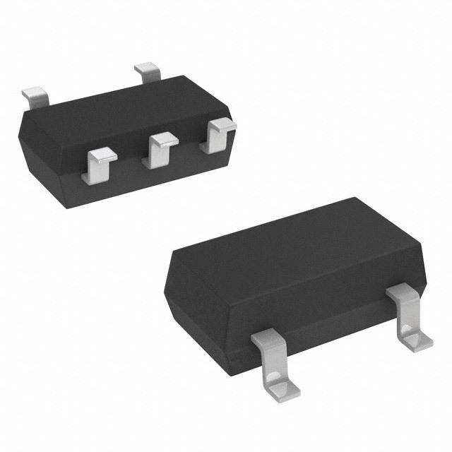
| 描述 | IC OPAMP CHOPPER 3MHZ RRO 8SO |
| 产品分类 | Linear - Amplifiers - Instrumentation, OP Amps, Buffer Amps |
| 品牌 | Linear Technology |
| 数据手册 | http://www.linear.com/docs/1799 |
| 产品图片 |
|
| 产品型号 | LTC2051IS8#PBF |
| rohs | 无铅 / 符合限制有害物质指令(RoHS)规范要求 |
| 产品系列 | - |
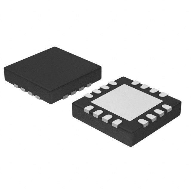
| 供应商器件封装 | 8-SO |
| 其它名称 | LTC2051IS8PBF |
| 包装 | 管件 |
| 压摆率 | 2 V/µs |
| 增益带宽积 | 3MHz |
| 安装类型 | 表面贴装 |
| 封装/外壳 | 8-SOIC(0.154",3.90mm 宽) |
| 工作温度 | -40°C ~ 85°C |
| 放大器类型 | 断路器(零漂移) |
| 标准包装 | 100 |
| 电压-电源,单/双 (±) | 2.7 V ~ 7 V |
| 电压-输入失调 | 0.5µV |
| 电流-电源 | 850µA |
| 电流-输入偏置 | 25pA |
| 电流-输出/通道 | - |
| 电路数 | 2 |
| 输出类型 | 满摆幅 |


- 商务部:美国ITC正式对集成电路等产品启动337调查
- 曝三星4nm工艺存在良率问题 高通将骁龙8 Gen1或转产台积电
- 太阳诱电将投资9.5亿元在常州建新厂生产MLCC 预计2023年完工
- 英特尔发布欧洲新工厂建设计划 深化IDM 2.0 战略
- 台积电先进制程称霸业界 有大客户加持明年业绩稳了
- 达到5530亿美元!SIA预计今年全球半导体销售额将创下新高
- 英特尔拟将自动驾驶子公司Mobileye上市 估值或超500亿美元
- 三星加码芯片和SET,合并消费电子和移动部门,撤换高东真等 CEO
- 三星电子宣布重大人事变动 还合并消费电子和移动部门
- 海关总署:前11个月进口集成电路产品价值2.52万亿元 增长14.8%


PDF Datasheet 数据手册内容提取
LTC2051/LTC2052 Dual/Quad Zero-Drift Operational Amplifiers FEATURES DESCRIPTIOU ■ Maximum Offset Voltage of 3μV The LTC®2051/LTC2052 are dual/quad zero-drift opera- ■ Maximum Offset Voltage Drift of 30nV/°C tional amplifiers available in the MS8 and SO-8/GN16 and ■ Small Footprint, Low Profile MS8/GN16 Packages S14 packages. For space limited applications, the LTC2051 ■ Single Supply Operation: 2.7V to ±5.5V is available in a 3mm × 3mm × 0.8mm dual fine pitch ■ Noise: 1.5μV (0.01Hz to 10Hz Typ) leadless package (DFN). They operate from a single 2.7V P-P ■ Voltage Gain: 140dB (Typ) supply and support ±5V applications. The current con- ■ PSRR: 130dB (Typ) sumption is 750μA per op amp. ■ CMRR: 130dB (Typ) The LTC2051/LTC2052, despite their miniature size, fea- ■ Supply Current: 0.75mA (Typ) per Amplifier ture uncompromising DC performance. The typical input ■ Extended Common Mode Input Range offset voltage and offset drift are 0.5μV and 10nV/°C. The ■ Output Swings Rail-to-Rail almost zero DC offset and drift are supported with a power ■ Operating Temperature Range –40°C to 125°C supply rejection ratio (PSRR) and common mode rejec- ■ Available in 3mm × 3mm × 0.8mm DFN Package tion ratio (CMRR) of more than 130dB. APPLICATIOU S The input common mode voltage ranges from the negative supply up to typically 1V from the positive supply. The ■ Thermocouple Amplifiers LTC2051/LTC2052 also have an enhanced output stage ■ Electronic Scales capable of driving loads as low as 2kΩ to both supply rails. ■ Medical Instrumentation The open-loop gain is typically 140dB. The LTC2051/ ■ Strain Gauge Amplifiers LTC2052 also feature a 1.5μV DC to 10Hz noise and a ■ High Resolution Data Acquisition P-P 3MHz gain-bandwidth product. ■ DC Accurate RC Active Filters ■ Low Side Current Sense , LT, LTC and LTM are registered trademarks of Linear Technology Corporation. All other trademarks are the property of their respective owners. TYPICAL APPLICATIOU High Performance Low Cost Instrumentation Amplifier Input Referred Noise 0.1Hz to 10Hz 2 R1 R2 100Ω 10k 0.1% 0.1% 1 R2 5V 10k R1 0.1% 2 – 8 100Ω Vμ 0 1/2 1 0.1% 6 – LTC2051HV –VIN 3 + LTC210/251HV 7 –1 VIN 5 + 4 AV = 101 –5V 20512 TA01 –2 0 2 4 6 8 10 TIME (SEC) 2052 TA02 20512fd 1
LTC2051/LTC2052 ABSOLUTE W AXIW UW RATIU GS (Note 1) Total Supply Voltage (V+ to V–) Operating Temperature Range............. –40°C to 125°C LTC2051/LTC2052 .................................................. 7V Specified Temperature Range (Note 3) –40°C to 125°C LTC2051HV/LTC2052HV....................................... 12V Storage Temperature Range................ –65°C to 150°C Input Voltage (Note 5)..........(V+ + 0.3V) to (V– – 0.3V) DD Package...................................... –65°C to 125°C Output Short-Circuit Duration......................... Indefinite Lead Temperature (Soldering, 10 sec)................. 300°C PACKAGE/ORDER IU FORW ATIOU TOP VIEW TOP VIEW TOP VIEW OUT A 1 8 V+ OUT A 1 8V+ OUT A 1 10 V+ –IN A 2 9 7 OUT B –IN A 2 7OUT B –IN A 2 9 OUT B +INV A– 43 56 –+IINN BB +INV A– 34 65–+IINN BB SH+DINNV AA– 345 876 –+SHIINND BBN B MS8 PACKAGE MS10 PACKAGE DD PACKAGE 8-LEAD PLASTIC MSOP 10-LEAD PLASTIC MSOP 8-LEAD (3mm × 3mm) PLASTIC DFN TJMAX = 125°C, θJA = 160°C/W TJMAX = 125°C, θJA = 250°C/W TJMAX = 125°C, θJA = 250°C/W EXPOSED PAD (PIN 9) IS CONNECTED TO V– (PIN 4) ORDER PART DD PART ORDER PART MS8 PART ORDER PART MS10 PART NUMBER* MARKING NUMBER MARKING NUMBER MARKING LTC2051CDD LAAN LTC2051CMS8 LTMN LTC2051CMS10 LTMQ LTC2051IDD LTC2051IMS8 LTMP LTC2051IMS10 LTMR LTC2051HVCDD LAEL LTC2051HVCMS8 LTPJ LTC2051HVCMS10 LTRB LTC2051HVIDD LTC2051HVIMS8 LTPK LTC2051HVIMS10 LTRC LTC2051HMS8 LTVF LTC2051HVHMS8 LTVH TOP VIEW ORDER PART S8 PART NUMBER MARKING OUT A 1 8 V+ –IN A 2 7 OUT B LTC2051CS8 2051 +IN A 3 6 –IN B LTC2051IS8 2051I V– 4 5 +IN B LTC2051HVCS8 2051HV LTC2051HVIS8 051HVI S8 PACKAGE 8-LEAD PLASTIC SO LTC2051HS8 2051H TJMAX = 125°C, θJA = 190°C/W LTC2051HVHS8 051HVH Order Options Tape and Reel: Add #TR Lead Free: Add #PBF Lead Free Tape and Reel: Add #TRPBF Lead Free Part Marking: http://www.linear.com/leadfree/ Consult LTC Marketing for parts specified with wider operating temperature ranges. 20512fd 2
LTC2051/LTC2052 PACKAGE/ORDER IU FORW ATIOU ORDER PART ORDER PART NUMBER NUMBER TOP VIEW LTC2052CGN TOP VIEW LTC2052CS OUT A 1 16 OUT D LTC2052IGN OUT A 1 14 OUT D LTC2052IS –IN A 2 15 –IN D LTC2052HVCGN –IN A 2 13 –IN D LTC2052HVCS +IN A 3 14 +IN D LTC2052HVIGN LTC2052HVIS V+ 4 13 V– +IN A 3 12 +IN D LTC2052HGN V+ 4 11 V– LTC2052HS +IN B 5 12 +IN C LTC2052HVHGN LTC2052HVHS +IN B 5 10 +IN C –IN B 6 11 –IN C –IN B 6 9 –IN C OUT B 7 10 OUT C GN PART MARKING OUT B 7 8 OUT C NC 8 9 NC 2052 S PACKAGE GN PACKAGE 2052I 14-LEAD PLASTIC SO 16-LEAD PLASTIC SSOP 2052HV TJMAX = 125°C, θJA = 110°C/W TJMAX = 125°C, θJA = 110°C/W 052HVI 2052H 052HVH AVAILABLE OPTIOU S PART NUMBER AMPS/PACKAGE SPECIFIED TEMP RANGE SPECIFIED VOLTAGE PACKAGE LTC2051CDD 2 0°C to 70°C 3V, 5V DD LTC2051CS8 2 0°C to 70°C 3V, 5V SO-8 LTC2051CMS8 2 0°C to 70°C 3V, 5V 8-Lead MSOP LTC2051CMS10 2 0°C to 70°C 3V, 5V 10-Lead MSOP LTC2051HVCDD 2 0°C to 70°C 3V, 5V, ±5V DD LTC2051HVCS8 2 0°C to 70°C 3V, 5V, ±5V SO-8 LTC2051HVCMS8 2 0°C to 70°C 3V, 5V, ±5V 8-Lead MSOP LTC2051HVCMS10 2 0°C to 70°C 3V, 5V, ±5V 10-Lead MSOP LTC2051IDD 2 –40°C to 85°C 3V, 5V DD LTC2051IS8 2 –40°C to 85°C 3V, 5V SO-8 LTC2051IMS8 2 –40°C to 85°C 3V, 5V 8-Lead MSOP LTC2051IMS10 2 –40°C to 85°C 3V, 5V 10-Lead MSOP LTC2051HVIDD 2 –40°C to 85°C 3V, 5V, ±5V DD LTC2051HVIS8 2 –40°C to 85°C 3V, 5V, ±5V SO-8 LTC2051HVIMS8 2 –40°C to 85°C 3V, 5V, ±5V 8-Lead MSOP LTC2051HVIMS10 2 –40°C to 85°C 3V, 5V, ±5V 10-Lead MSOP LTC2051HS8 2 –40°C to 125°C 3V, 5V SO-8 LTC2051HMS8 2 –40°C to 125°C 3V, 5V 8-Lead MSOP LTC2051HVHS8 2 –40°C to 125°C 3V, 5V, ±5V SO-8 LTC2051HVHMS8 2 –40°C to 125°C 3V, 5V, ±5V 8-Lead MSOP LTC2052CS 4 0°C to 70°C 3V, 5V 14-Lead SO LTC2052CGN 4 0°C to 70°C 3V, 5V 16-Lead SSOP LTC2052HVCS 4 0°C to 70°C 3V, 5V, ±5V 14-Lead SO LTC2052HVCGN 4 0°C to 70°C 3V, 5V, ±5V 16-Lead SSOP 20512fd 3
LTC2051/LTC2052 AVAILABLE OPTIOU S PART NUMBER AMPS/PACKAGE SPECIFIED TEMP RANGE SPECIFIED VOLTAGE PACKAGE LTC2052IS 4 –40°C to 85°C 3V, 5V 14-Lead SO LTC2052IGN 4 –40°C to 85°C 3V, 5V 16-Lead SSOP LTC2052HVIS 4 –40°C to 85°C 3V, 5V, ±5V 14-Lead SO LTC2052HVIGN 4 –40°C to 85°C 3V, 5V, ±5V 16-Lead SSOP LTC2052HS 4 –40°C to 125°C 3V, 5V 14-Lead SO LTC2052HGN 4 –40°C to 125°C 3V, 5V 16-Lead SSOP LTC2052HVHS 4 –40°C to 125°C 3V, 5V, ±5V 14-Lead SO LTC2052HVHGN 4 –40°C to 125°C 3V, 5V, ±5V 16-Lead SSOP ELECTRICAL CHARACTERISTICS (LTC2051/LTC2052, LTC2051HV/LTC2052HV) The ● denotes the specifications which apply over the full operating temperature range, otherwise specifications are at TA = 25°C. VS = 3V, 5V unless otherwise noted. (Note 3) LTC2051C/LTC2052C LTC2051I/LTC2052I LTC2051H/LTC2052H PARAMETER CONDITIONS MIN TYP MAX MIN TYP MAX UNITS Input Offset Voltage (Note 2) ±0.5 ±3 ±0.5 ±3 μV Average Input Offset Drift (Note 2) ● 0.01 ±0.03 0.01 ±0.05 μV/°C Long-Term Offset Drift 50 50 nV/√mo Input Bias Current (Note 4) VS = 3V ±8 ±50 ±8 ±50 pA VS = 3V ● ±100 ±3000 pA VS = 5V ±25 ±75 ±25 ±75 pA VS = 5V ● ±150 ±3000 pA Input Offset Current (Note 4) VS = 3V ±100 ±100 pA VS = 3V ● ±150 ±700 pA VS = 5V ±150 ±150 pA VS = 5V ● ±200 ±700 pA Input Noise Voltage RS = 100Ω, DC to 10Hz 1.5 1.5 μVP-P Common Mode Rejection Ratio V = GND to V+ – 1.3, 115 130 115 130 dB CM V = 3V ● 110 130 110 130 dB S V = GND to V+ – 1.3, 120 130 120 130 dB CM V = 5V ● 115 130 115 130 dB S Power Supply Rejection Ratio 120 130 120 130 dB ● 115 130 115 130 dB Large-Signal Voltage Gain R = 10k, V = 3V 120 140 120 140 dB L S ● 115 140 115 140 dB R = 10k, V = 5V 125 140 125 140 dB L S ● 120 140 120 140 dB Output Voltage Swing High R = 2k to GND ● V+ – 0.15 V+ – 0.06 V+ – 0.15 V+ – 0.06 V L R = 10k to GND ● V+ – 0.05 V+ – 0.02 V+ – 0.05 V+ – 0.02 V L Output Voltage Swing Low R = 2k to GND ● 2 15 2 15 mV L R = 10k to GND ● 2 15 2 15 mV L Slew Rate 2 2 V/μs Gain Bandwidth Product 3 3 MHz Supply Current (Per Amplifier) No Load, V = 3V, V = V ● 0.75 1.0 0.75 1.1 mA S SHDN IH No Load, V = 5V, V = V ● 0.85 1.2 0.85 1.3 mA S SHDN IH Supply Current, Shutdown VSHDN = VIL, VS = 3V ● 2 5 2 5 μA VSHDN = VIL, VS = 5V ● 4 10 4 10 μA 20512fd 4
LTC2051/LTC2052 ELECTRICAL CHARACTERISTICS (LTC2051/LTC2052, LTC2051HV/LTC2052HV) The ● denotes the specifications which apply over the full operating temperature range, otherwise specifications are at TA = 25°C. VS = 3V, 5V unless otherwise noted. (Note 3) LTC2051C/LTC2052C LTC2051I/LTC2052I LTC2051H/LTC2052H PARAMETER CONDITIONS MIN TYP MAX MIN TYP MAX UNITS Shutdown Pin Input Low Voltage (V ) ● V– + 0.5 V– + 0.5 V IL Shutdown Pin Input High Voltage (V ) ● V+ – 0.5 V+ – 0.5 V IH Shutdown Pin Input Current VSHDN = VIL, VS = 3V ● –1 –3 –1 –3 μA VSHDN = VIL, VS = 5V ● –2 –5 –2 –5 μA Internal Sampling Frequency 7.5 7.5 kHz (LTC2051HV/LTC2052HV) The ● denotes the specifications which apply over the full operating temperature range, otherwise specifications are at TA = 25°C. VS = ±5V unless otherwise noted. (Note 3) LTC2051C/LTC2052C LTC2051I/LTC2052I LTC2051H/LTC2052H PARAMETER CONDITIONS MIN TYP MAX MIN TYP MAX UNITS Input Offset Voltage (Note 2) ±1 ±3 ±1 ±3 μV Average Input Offset Drift (Note 2) ● 0.01 ±0.03 0.01 ±0.05 μV/°C Long-Term Offset Drift 50 50 nV/√mo Input Bias Current (Note 4) ±90 ±150 ±90 ±150 pA ● ±300 ±3000 pA Input Offset Current (Note 4) ±300 ±300 pA ● ±500 ±700 pA Input Noise Voltage RS = 100Ω, DC to 10Hz 1.5 1.5 μVP-P Common Mode Rejection Ratio V = V– to V+ – 1.3 125 130 125 130 dB CM ● 120 130 120 130 dB Power Supply Rejection Ratio 120 130 120 130 dB ● 115 130 115 130 dB Large-Signal Voltage Gain R = 10k 125 140 125 140 dB L ● 120 140 120 140 dB Maximum Output Voltage Swing RL = 2k to GND ● ±4.75 ±4.92 ±4.50 ±4.92 V RL = 10k to GND ● ±4.90 ±4.98 ±4.85 ±4.98 V Slew Rate 2 2 V/μs Gain Bandwidth Product 3 3 MHz Supply Current (Per Amplifier) No Load, V = V ● 1 1.5 1 1.5 mA SHDN IH Supply Current, Shutdown VSHDN = VIL ● 15 30 15 30 μA Shutdown Pin Input Low Voltage (V ) ● V– + 0.5 V– + 0.5 V IL Shutdown Pin Input High Voltage (V ) ● V+ – 0.5 V+ – 0.5 V IH Shutdown Pin Input Current VSHDN = VIL ● –7 –15 –7 –15 μA Internal Sampling Frequency 7.5 7.5 kHz Note 1: Stresses beyond those listed under Absolute Maximum Ratings are guaranteed to meet the temperature limits of –40°C and 125°C. may cause permanent damage to the device. Exposure to any Absolute Note 4: The bias current measurement accuracy depends on the proximity of Maximum Rating condition for extended periods may affect device the negative supply bypass capacitors to the device under test. Because of reliability and lifetime. this, only the bias current of channel B (LTC2051) and channels A and B Note 2: These parameters are guaranteed by design. Thermocouple effects (LTC2052) are 100% tested to the data sheet specifications. The bias preclude measurements of these voltage levels during automated testing. currents of the remaining channels are 100% tested to relaxed limits, Note 3: All versions of the LTC2051/LTC2052 are designed, characterized however, their values are guaranteed by design to meet the data sheet limits. and expected to meet the extended temperature limits of –40°C and 125°C. Note 5: This parameter is guaranteed to meet specified performance The LTC2051C/LTC2052C/LTC2051HVC/LTC2052HVC are guaranteed to through design and characterization. It has not been tested. meet the temperature limits of 0°C and 70°C. The LTC2051I/LTC2052I/ Note 6: The θJA specified for the DD package is with minimal PCB heat LTC2051HVI/LTC2052HVI are guaranteed to meet temperature limits of – spreading metal. Using expanded metal area on all layers of a board 40°C and 85°C. The LTC2051H/LTC2051HVH and LTC2052H/LTC2052HVH reduces this value. 20512fd 5
LTC2051/LTC2052 TYPICAL PERFORW AU CE CHARACTERISTICS Common Mode Rejection Ratio DC CMRR vs Frequency vs Common Mode Input Range PSRR vs Frequency 140 140 120 VS = 3V OR ±5V VCM = 0.5VP-P 120 120 100 VS = 10V –PSRR 100 100 80 VS = 3V VS = 5V R (dB) 80 R (dB) 80 R (dB) 60 MR 60 MR 60 SR +PSRR C C P 40 40 40 20 20 20 0 0 0 1 10 100 1k 10k 100k 0 2 4 6 8 10 10 100 1k 10k 100k 1M FREQUENCY (Hz) VCM (V) FREQUENCY (Hz) 20512 G01 20512 G03 20512 G02 Output Voltage Swing Output Swing vs Load Resistance Output Swing vs Output Current vs Load Resistance ±5V 6 6 5 RL TO GND 5 VS = 5V 5 VS = 5V 4 RL TO GND 3 NG (V) 4 AGE (V) 4 AGE (V) 21 SWI 3 VS = 3V OLT 3 VS = 3V OLT 0 PUT UT V UT V –1 T P P U 2 T 2 T O OU OU –2 –3 1 1 –4 0 0 –5 0 2 4 6 8 10 0.01 0.1 1 10 0 2 4 6 8 10 LOAD RESISTANCE (kΩ) OUTPUT CURRENT (mA) LOAD RESISTANCE (kΩ) 20512 G04 20512 G05 20512 G06 Output Swing vs Output Current, ±5V Supply Gain/Phase vs Frequency Bias Current vs Temperature 5 100 80 10k PHASE 4 RL TO GND 80 100 3 1k OUTPUT SWING (V) ––11220 GAIN (dB) 4260000 GAIN 111462000PHASE (DEG) BIAS CURRENT (pA)100 VVSS = = ± 55VV 10 VS = 3V –3 –20 VS = 3V OR ±5V 180 –4 CL = 50pF RL = 100k –5 –40 200 1 0.01 0.1 1 10 100 1k 10k 100k 1M 10M –50 0 50 100 125 OUTPUT CURRENT (mA) FREQUENCY (Hz) TEMPERATURE (°C) 20512 G07 20512 G08 20512 G09 20512fd 6
LTC2051/LTC2052 TYPICAL PERFORW AU CE CHARACTERISTICS Input Bias Current vs Input Common Mode Voltage Transient Response Input Overload Recovery 250 V) T ( 0 U A) 200 INP–0.1 p T ( V RREN 150 2V/DI V) 1.5 CU T ( BIAS 100 UTPU UT VS = ±5V O 0 P N I 50 VS = 5V AV = 1 1μs/DIV 20512 G11 AV = –100 500μs/DIV 2050 G12 VS = 3V RL = 10k RL = 100k 0 CL = 100pF CL = 10pF –5 –3 –1 0 1 3 5 VS = ±5V VS = 3V INPUT COMMON MODE VOLTAGE (V) 20512 G10 Sampling Frequency Sampling Frequency vs Supply Voltage vs Temperature 10 10 Hz) 9 Hz) 9 k k Y ( Y ( C C UEN 8 UEN 8 VS = ±5V Q Q E E FR FR VS = 3V G 7 G 7 N N LI LI P P M M SA 6 SA 6 5 5 3 5 7 9 11 –50 0 50 100 125 SUPPLY VOLTAGE (V) TEMPERATURE (°C) 20512 G13 20512 G14 Supply Current (Per Amplifier) Supply Current (Per Amplifier) vs Supply Voltage vs Temperature 1.2 1.2 VS = ±5V 1.0 1.0 NT (mA) 0.8 NT (mA) 0.8 VS = 5V RE RE UR 0.6 UR 0.6 VS = 3V C C Y Y PPL 0.4 PPL 0.4 U U S S 0.2 0.2 0 0 2.5 4.5 6.5 8.5 10.5 –50 0 50 100 125 SUPPLY VOLTAGE (V) TEMPERATURE (°C) 20512 G15 20512 G16 20512fd 7
LTC2051/LTC2052 APPLICATIOU S IU FORW ATIOU Shutdown To reduce this form of clock feedthrough, use smaller valued gain setting resistors and minimize the source The LTC2051 includes a shutdown pin in the 10-lead resistance at the input. If the resistance seen at the inputs MSOP. When this active low pin is high or allowed to float, is less than 10k, this form of clock feedthrough is less the device operates normally. When the shutdown pin is than 1μV input referred at 7.5kHz, or less than the pulled low, the device enters shutdown mode; supply RMS amount of residue clock feedthrough from the first form current drops to 3μA, all clocking stops and the output previously described. assumes a high impedance state. Placing a capacitor across the feedback resistor reduces Clock Feedthrough, Input Bias Current either form of clock feedthrough by limiting the bandwidth of the closed-loop gain. The LTC2051/LTC2052 use autozeroing circuitry to achieve an almost zero DC offset over temperature, common Input bias current is defined as the DC current into the mode voltage and power supply voltage. The frequency of input pins of the op amp. The same current spikes that the clock used for autozeroing is typically 7.5kHz. The cause the second form of clock feedthrough previously term clock feedthrough is broadly used to indicate visibil- described, when averaged, dominate the DC input bias ity of this clock frequency in the op amp output spectrum. current of the op amp below 70°C. There are typically two types of clock feedthrough in At temperatures above 70°C, the leakage of the ESD autozeroed op amps like the LTC2051/LTC2052. protection diodes on the inputs increase the input bias The first form of clock feedthough is caused by the settling currents of both inputs in the positive direction, while the of the internal sampling capacitor and is input referred; current caused by the charge injection stays relatively that is, it is multiplied by the closed-loop gain of the op constant. At elevated temperatures (above 85°C) the amp. This form of clock feedthrough is independent of the leakage current begins to dominate and both the negative magnitude of the input source resistance or the magnitude and positive pin’s input bias currents are in the positive of the gain setting resistors. The LTC2051/LTC2052 have direction (into the pins). a residue clock feedthrough of less than 1μV input RMS referred at 7.5kHz. Input Pins, ESD Sensitivity The second form of clock feedthrough is caused by the ESD voltages above 700V on the input pins of the op amp small amount of charge injection occurring during the will cause the input bias currents to increase (more DC sampling and holding of the op amps input offset voltage. current into the pins). At these voltages, it is possible to The current spikes are multiplied by the impedance seen damage the device to a point where the input bias current at the input terminals of the op amp, appearing at the exceeds the maximums specified in this data sheet. output multiplied by the closed-loop gain of the op amp. TYPICAL APPLICATIOU The dual chopper op amp buffers the inputs of A1 and needed and the input source resistance is low. (For in- corrects its offset voltage and offset voltage drift. With the stance a 350Ω strain gauge bridge.) The LT1012 or RC values shown, the power-up warm-up time is typically equivalent should be used when low bias current (100pA) 20 seconds. The step response of the composite amplifier is also required in conjunction with DC to 10Hz low noise, does not present settling tails. The LT®1677 should be low V and V drift. The measured typical input offset OS OS used when extremely low noise, V and V drift are voltages are less than 1μV. OS OS 20512fd 8
LTC2051/LTC2052 TYPICAL APPLICATIOU Obtaining Ultralow V Drift and Low Noise OS + 5 + 2 – 1/2 LTC2051 7 1 R4 6 1/2 LTC2051 – 3 + 5V R5 C1 OUT C2 20512 F01 R1 R2 R3 3 + 1 8 6 A1 OUT 2 – – A1 R1 R2 R3 R4 R5 C1 C2 e (DC – 1Hz) e (DC – 10Hz) IN IN LT1677 2.49k 3.01k 340k 10k 100k 0.01μF 0.001μF 0.15μVP-P 0.2μVP-P LT1012 750Ω 57Ω 250k 10k 100k 0.01μF 0.001μF 0.3μVP-P 0.4μVP-P PACKAGE DESCRIPTIOU DD Package 8-Lead Plastic DFN (3mm × 3mm) (Reference LTC DWG # 05-08-1698) R = 0.115 0.38 ± 0.10 TYP 5 8 0.675 ±0.05 3.00 ±0.10 1.65 ± 0.10 3.5 ±0.05 1.65 ±0.05 (4 SIDES) (2 SIDES) 2.15 ±0.05 (2 SIDES) PIN 1 TOP MARK PACKAGE (NOTE 6) OUTLINE 4 1 0.200 REF 0.75 ±0.05 0.25 ± 0.05 0.25 ± 0.05 0.50 BSC 0.50 2.38 ±0.10 BSC 0.00 – 0.05 (2 SIDES) 2.38 ±0.05 BOTTOM VIEW—EXPOSED PAD (2 SIDES) NOTE: RECOMMENDED SOLDER PAD PITCH AND DIMENSIONS 1. DRAWING TO BE MADE A JEDEC PACKAGE OUTLINE M0-229 VARIATION OF (WEED-1) (DD) DFN 1203 2. DRAWING NOT TO SCALE 3. ALL DIMENSIONS ARE IN MILLIMETERS 4. DIMENSIONS OF EXPOSED PAD ON BOTTOM OF PACKAGE DO NOT INCLUDE MOLD FLASH. MOLD FLASH, IF PRESENT, SHALL NOT EXCEED 0.15mm ON ANY SIDE 5. EXPOSED PAD SHALL BE SOLDER PLATED 6. SHADED AREA IS ONLY A REFERENCE FOR PIN 1 LOCATION ON TOP AND BOTTOM OF PACKAGE 20512fd 9
LTC2051/LTC2052 PACKAGE DESCRIPTIOU MS8 Package 8-Lead Plastic MSOP (Reference LTC DWG # 05-08-1660) DETAIL “A” 0.254 (.010) 0° – 6° TYP GAUGE PLANE 3.00 ± 0.102 0.53 ± 0.152 (.118 ± .004) 0.52 DETAIL “A” (.021 ± .006) (M1.0.A1403X) (0.R0.E83F64) (NOTE 3) 8 7 6 5 (.0R2E0F5) 0(..083859 ±± 0.0.10257) 0.18 (.007) 4.90 ± 0.152 3.00 ± 0.102 SEPALTAINNGE 0.22 – 0.38 0.127 ± 0.076 (.193 ± .006) (.1(1N8O ±TE . 040)4) (5.M2.20IN36) (3.1.2206 –– 3.1.4356) (.009T Y–P .015) 0.65 (.005 ± .003) NOTE: (.0256) 1. DIMENSIONS IN MILLIMETER/(INCH) BSC 1 2 3 4 2. DRAWING NOT TO SCALE 0.42 ± 0.038 0.65 3. DIMENSION DOES NOT INCLUDE MOLD FLASH, PROTRUSIONS OR GATE BURRS. (.0165 ± .0015) (.0256) MOLD FLASH, PROTRUSIONS OR GATE BURRS SHALL NOT EXCEED 0.152mm (.006") PER SIDE TYP BSC 4. DIMENSION DOES NOT INCLUDE INTERLEAD FLASH OR PROTRUSIONS. RECOMMENDED SOLDER PAD LAYOUT INTERLEAD FLASH OR PROTRUSIONS SHALL NOT EXCEED 0.152mm (.006") PER SIDE 5. LEAD COPLANARITY (BOTTOM OF LEADS AFTER FORMING) SHALL BE 0.102mm (.004") MAX MSOP (MS8) 0204 MS Package 10-Lead Plastic MSOP (Reference LTC DWG # 05-08-1661) 3.00 ± 0.102 (.118 ± .004) 0.497 ± 0.076 (NOTE 3) 109 8 76 (.019R6 E±F .003) 0.889 ± 0.127 (.035 ± .005) 4.90 ± 0.152 3.00 ± 0.102 0.254 DETAIL “A” (.193 ± .006) (.1(1N8O ±TE . 040)4) (5.2.2036) 3.20 – 3.45 (.010) 0° – 6° TYP MIN (.126 – .136) GAUGE PLANE 1 2 3 4 5 0.53 ± 0.152 0.305 ± 0.038 0.50 (.021 ± .006) 1.10 0.86 (.0120T Y±P .0015) (.0B1S9C7) (.043) (.034) DETAIL “A” MAX REF RECOMMENDED SOLDER PAD LAYOUT 0.18 MSOP (MS) 0603 (.007) SEATING PLANE 0.17 – 0.27 0.127 ± 0.076 (.007 – .011) 0.50 (.005 ± .003) TYP NOTE: (.0197) 1. DIMENSIONS IN MILLIMETER/(INCH) BSC 2. DRAWING NOT TO SCALE 3. DIMENSION DOES NOT INCLUDE MOLD FLASH, PROTRUSIONS OR GATE BURRS. MOLD FLASH, PROTRUSIONS OR GATE BURRS SHALL NOT EXCEED 0.152mm (.006") PER SIDE 4. DIMENSION DOES NOT INCLUDE INTERLEAD FLASH OR PROTRUSIONS. INTERLEAD FLASH OR PROTRUSIONS SHALL NOT EXCEED 0.152mm (.006") PER SIDE 5. LEAD COPLANARITY (BOTTOM OF LEADS AFTER FORMING) SHALL BE 0.102mm (.004") MAX 20512fd 10
LTC2051/LTC2052 PACKAGE DESCRIPTIOU S8 Package 8-Lead Plastic Small Outline (Narrow .150 Inch) (Reference LTC DWG # 05-08-1610) .189 – .197 (4.801 – 5.004) NOTE 3 (0..021504 –– .00.25008)× 45°(cid:31) .053 – .069 .004 – .010 8 7 6 5 .050 BSC .045 ±.005 (1.346 – 1.752) (0.101 – 0.254) .008 – .010 (0.203 – 0.254) 0°– 8° TYP .150 – .157 .228 – .244 .245 (0..041066 –– .10.52070) .014 – .019 .050 (5.791 – 6.197) (3.81N0O T–E 3 3.988) MIN .160 ±.005 (0.355 – 0.483) (1.270) NOTE: INCHES TYP BSC SO8 0303 1. DIMENSIONS IN (MILLIMETERS) 2. DRAWING NOT TO SCALE 3. THESE DIMENSIONS DO NOT INCLUDE MOLD FLASH OR PROTRUSIONS. 1 2 3 4 .030 ±.005 MOLD FLASH OR PROTRUSIONS SHALL NOT EXCEED .006" (0.15mm) TYP RECOMMENDED SOLDER PAD LAYOUT GN Package 16-Lead Plastic SSOP (Narrow .150 Inch) (Reference LTC DWG # 05-08-1641) ( 0.0.3185 ±± 0.0.1004)× 45° .(015.3325 –– .10.67858) (0.0.10042 – – . 000.29489) ( 4 ..188091 –– .41.9967*8) .045 ±.005 (0.0.10778 – – . 000.29489) 0° – 8° TYP (0.0.20299) 16 1514131211109 REF .016 – .050 .008 – .012 .0250 (0.406 – 1.270) (0.203 – 0.305) (0.635) .254 MIN .150 – .165 TYP BSC NOTE: .229 – .244 .150 – .157** 1. CONTROLLING DIMENSION: INCHES (5.817 – 6.198) (3.810 – 3.988) 2. DIMENSIONS ARE IN(MILILNICMHEETSERS) 3. DRAWING NOT TO SCALE .0165 ±.0015 .0250 BSC * DIMENSION DOES NOT INCLUDE MOLD FLASH. MOLD FLASH SHALL NOT EXCEED 0.006" (0.152mm) PER SIDE RECOMMENDED SOLDER PAD LAYOUT **D IMENSION DOES NOT INCLUDE INTERLEAD FLASH. INTERLEAD FLASH SHALL NOT EXCEED 0.010" (0.254mm) PER SIDE 1 2 3 4 5 6 7 8 GN16 (SSOP) 0204 S Package 14-Lead Plastic Small Outline (Narrow .150 Inch) (Reference LTC DWG # 05-08-1610) .337 – .344 .045 ±.005 (8.560 – 8.738) .050 BSC NOTE 3 14 13 12 11 10 9 8 N N .245 MIN .160 ±.005 .228 – .244 .150 – .157 (5.791 – 6.197) (3.810 – 3.988) NOTE 3 1 2 3 N/2 N/2 .030 ±.005 TYP RECOMMENDED SOLDER PAD LAYOUT 1 2 3 4 5 6 7 .010 – .020 × 45° .053 – .069 (0.254 – 0.508) (1.346 – 1.752) .008 – .010 .004 – .010 (0.203 – 0.254) 0° – 8° TYP (0.101 – 0.254) .016 – .050 .014 – .019 .050 (0.406 – 1.270) (0.355 – 0.483) (1.270) TYP BSC NOTE: INCHES S14 0502 1. DIMENSIONS IN (MILLIMETERS) 2. DRAWING NOT TO SCALE 3. THESE DIMENSIONS DO NOT INCLUDE MOLD FLASH OR PROTRUSIONS. MOLD FLASH OR PROTRUSIONS SHALL NOT EXCEED .006" (0.15mm) 20512fd Information furnished by Linear Technology Corporation is believed to be accurate and reliable. 11 However, no responsibility is assumed for its use. Linear Technology Corporation makes no represen- tation that the interconnection of its circuits as described herein will not infringe on existing patent rights.
LTC2051/LTC2052 TYPICAL APPLICATIOU Paralleling Amplifiers to Improve Noise R2 R1 2 – 1 R 1/4 LTC2052 3 + R 5V R2 R1 6 0.1μF VIN – 7 R 13 4 1/4 LTC2052 – 5 + 1/4 LTC2052 14 VOUT 12 + 11 R2 0.1μF R1 9 –5V – 8 R 1/4 LTC2052 10 + VOUT R2 NOISE OF EACH PARALLEL OP AMP VIN = 3R1; INPUT DC – 10Hz NOISE ≅ 0.8μVP-P = √3 20512 F02 RELATED PARTS PART NUMBER DESCRIPTION COMMENTS LTC1051/LTC1053 Precision Zero-Drift Op Amp Dual/Quad LTC1151 ±15V Zero-Drift Op Amp Dual High Voltage Operation ±18V LTC1152 Rail-to-Rail Input and Output Zero-Drift Op Amp Single Zero-Drift Op Amp with Rail-to-Rail Input and Output and Shutdown LTC2050 Zero-Drift Op Amp in SOT-23 Single Supply Operation 2.7V to ±5V, Shutdown LTC2053 Zero-Drift Precision Instrumentation Amp MS8, 116dB CMRR, Two External Resistors Set Gain LTC6800 Rail-to-Rail Input and Output Instrumentation Amp Low Cost, MS8, Two External Resistors Set Gain 20512fd 12 Linear Technology Corporation LT 0108 REV D • PRINTED IN USA 1630 McCarthy Blvd., Milpitas, CA 95035-7417 (408) 432-1900 ● FAX: (408) 434-0507 ● www.linear.com © LINEAR TECHNOLOGY CORPORATION 2000
Mouser Electronics Authorized Distributor Click to View Pricing, Inventory, Delivery & Lifecycle Information: A nalog Devices Inc.: LTC2052HGN#TRPBF LTC2051HVIDD#TRPBF LTC2052IGN#PBF LTC2052HVCS#PBF LTC2051HVIS8#PBF LTC2051HVCS8#TR LTC2051HVCMS10 LTC2051CDD#PBF LTC2051HVIDD LTC2051CMS8 LTC2052HVHS#TRPBF LTC2051HVIMS8#TR LTC2052HVHGN LTC2051HVCMS8#TR LTC2052IS LTC2051HMS8#TR LTC2052CGN#PBF LTC2051IMS8#TR LTC2052HVIGN#TR LTC2051CMS8#TRPBF LTC2052HVHGN#TRPBF LTC2051IDD LTC2051HVIMS10#TR LTC2051HVCMS10#TRPBF LTC2052CS LTC2052HS#TRPBF LTC2051IMS8 LTC2051HS8#TR LTC2052IS#TRPBF LTC2052HVIS#PBF LTC2051CMS8#PBF LTC2051HVHMS8#PBF LTC2052HS#TR LTC2051HMS8#TRPBF LTC2051HS8#PBF LTC2051HVCMS8 LTC2052HVIGN#TRPBF LTC2051HVIS8#TR LTC2052HVHGN#PBF LTC2052HVCS#TR LTC2052CGN#TR LTC2052HS LTC2051CMS10#PBF LTC2051HVIMS10#TRPBF LTC2051IMS10 LTC2052IS#PBF LTC2051CS8 LTC2052HVCGN#TR LTC2051HVCDD#PBF LTC2052CS#PBF LTC2051IDD#PBF LTC2051HVHS8#PBF LTC2051HVIMS10#PBF LTC2051HVCMS8#TRPBF LTC2052HVIS LTC2052IS#TR LTC2051CDD#TRPBF LTC2051IDD#TR LTC2052HVHGN#TR LTC2051HVIS8#TRPBF LTC2051HS8#TRPBF LTC2051HVIMS8 LTC2051IMS8#TRPBF LTC2051HVHMS8#TRPBF LTC2051CS8#PBF LTC2051HVIMS8#TRPBF LTC2052HVHS#PBF LTC2051HVIDD#PBF LTC2052HGN#PBF LTC2051HVCMS8#PBF LTC2052CS#TR LTC2052HVIS#TRPBF LTC2051IMS10#PBF LTC2051HVCDD#TR LTC2051IS8#TRPBF LTC2052HGN LTC2051HVHS8#TR LTC2051CMS10#TR LTC2052IGN LTC2051HVCDD LTC2051HVCS8#TRPBF LTC2051HVIMS8#PBF LTC2052HVCGN LTC2052IGN#TR LTC2051HMS8 LTC2051IDD#TRPBF LTC2051HVHS8#TRPBF LTC2052HVCGN#TRPBF LTC2052HVIGN LTC2052HGN#TR LTC2051HS8 LTC2052IGN#TRPBF LTC2051HVCMS10#PBF LTC2051HVCMS10#TR LTC2052HS#PBF LTC2052CS#TRPBF LTC2052HVCS LTC2051CMS10#TRPBF LTC2051HVHMS8 LTC2051CDD