ICGOO在线商城 > 集成电路(IC) > 线性 - 放大器 - 仪表,运算放大器,缓冲器放大器 > EL5462ISZ

 Datasheet下载
- 型号: EL5462ISZ
- 制造商: Intersil
- 库位|库存: xxxx|xxxx
- 要求:
| 数量阶梯 | 香港交货 | 国内含税 |
| +xxxx | $xxxx | ¥xxxx |
查看当月历史价格
查看今年历史价格
EL5462ISZ产品简介:
ICGOO电子元器件商城为您提供EL5462ISZ由Intersil设计生产,在icgoo商城现货销售,并且可以通过原厂、代理商等渠道进行代购。 EL5462ISZ价格参考¥16.86-¥33.94。IntersilEL5462ISZ封装/规格:线性 - 放大器 - 仪表,运算放大器,缓冲器放大器, 电流反馈 放大器 4 电路 14-SOIC。您可以下载EL5462ISZ参考资料、Datasheet数据手册功能说明书,资料中有EL5462ISZ 详细功能的应用电路图电压和使用方法及教程。
EL5462ISZ 是由 Renesas Electronics America Inc. 生产的一款线性放大器,属于仪表、运算放大器和缓冲器放大器类别。该型号具有低噪声、高精度以及宽频带特性,适用于多种精密信号处理场景。以下是其主要应用场景:

1. 工业自动化与控制
   EL5462ISZ 可用于工业自动化设备中的信号调理电路,例如传感器信号放大和滤波。它能够精确地处理来自压力、温度或位置传感器的微弱信号,确保数据采集系统的准确性。

2. 医疗设备
   在医疗领域,这款放大器适合用在心电图(ECG)、脑电图(EEG)等生物医学仪器中。其低噪声性能可以有效放大人体微弱的生理电信号,同时减少干扰,提供更清晰的诊断结果。

3. 测试测量仪器
   EL5462ISZ 常被集成到示波器、信号发生器和其他测试设备中,用于提高输入信号的质量和稳定性。它的高精度特性有助于实现更准确的测量结果。

4. 音频处理
   该放大器也可应用于高品质音频设备中,如前置放大器或麦克风信号增强器。凭借其优异的线性度和低失真特性,可显著改善音质表现。

5. 通信系统
   在无线通信基站或有线网络设备中,EL5462ISZ 能够优化射频前端模块的信号增益控制,从而提升整体传输效率和可靠性。

综上所述,EL5462ISZ 凭借其卓越的技术参数,在需要高精度、低噪声和稳定性能的各种电子应用中表现出色,是许多关键系统设计的理想选择。
| 参数 | 数值 |
| -3db带宽 | 500MHz |
| 产品目录 | 集成电路 (IC) |
| 描述 | IC OPAMP CFA 500MHZ 14SOIC |
| 产品分类 | Linear - Amplifiers - Instrumentation, OP Amps, Buffer Amps |
| 品牌 | Intersil |
| 数据手册 | |
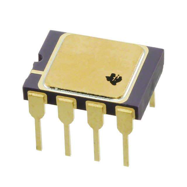
| 产品图片 |
|
| 产品型号 | EL5462ISZ |
| PCN组件/产地 | |
| rohs | 无铅 / 符合限制有害物质指令(RoHS)规范要求 |
| 产品系列 | - |
| 产品目录页面 | |
| 供应商器件封装 | 14-SOIC |
| 包装 | 管件 |
| 压摆率 | 4000 V/µs |
| 增益带宽积 | - |
| 安装类型 | 表面贴装 |
| 封装/外壳 | 14-SOIC(0.154",3.90mm 宽) |
| 工作温度 | -40°C ~ 85°C |
| 放大器类型 | 电流反馈 |
| 标准包装 | 55 |
| 电压-电源,单/双 (±) | 5 V ~ 12 V, ±2.5 V ~ 6 V |
| 电压-输入失调 | 1.5mV |
| 电流-电源 | 1.5mA |
| 电流-输入偏置 | 2µA |
| 电流-输出/通道 | 100mA |
| 电路数 | 4 |
| 输出类型 | - |


- 商务部:美国ITC正式对集成电路等产品启动337调查
- 曝三星4nm工艺存在良率问题 高通将骁龙8 Gen1或转产台积电
- 太阳诱电将投资9.5亿元在常州建新厂生产MLCC 预计2023年完工
- 英特尔发布欧洲新工厂建设计划 深化IDM 2.0 战略
- 台积电先进制程称霸业界 有大客户加持明年业绩稳了
- 达到5530亿美元!SIA预计今年全球半导体销售额将创下新高
- 英特尔拟将自动驾驶子公司Mobileye上市 估值或超500亿美元
- 三星加码芯片和SET,合并消费电子和移动部门,撤换高东真等 CEO
- 三星电子宣布重大人事变动 还合并消费电子和移动部门
- 海关总署:前11个月进口集成电路产品价值2.52万亿元 增长14.8%


PDF Datasheet 数据手册内容提取
DATASHEET EL5462 FN7492 500MHz Low Power Current Feedback Amplifier Rev 0.00 February 14, 2005 The EL5462 is a current feedback amplifier with a bandwidth Features of 500MHz which makes this amplifier ideal for today’s high • 500MHz -3dB bandwidth speed video and monitor applications. • 4000V/µs slew rate With a supply current of just 1.5mA per amplifier and the ability to run from a single supply voltage from 5V to 12V, the • 1.5mA supply current per amplifier EL5462 is also ideal for handheld, portable or battery- • Single and dual supply operation, from 5V to 12V supply powered equipment. span The EL5462 is available in a 14-pin SO package and • High speed, 1.4GHz product available (EL5167 & operates over the industrial temperature range of -40°C to EL5167) +85°C. • High speed, 4mA, 630MHz product available (EL5164 & Pinout EL5165) • Pb-free available (RoHS compliant) EL5462 (14-PIN SO) Applications TOP VIEW • Battery-powered equipment OUTA 1 14OUTD • Handheld, portable devices A D INA- 2 - + + - 13IND- • Video amplifiers INA+ 3 12IND+ • Cable drivers VS+ 4 11VS- • RGB amplifiers INB+ 5 10INC+ • Test equipment INB- 6 -B+ +C- 9 INC- • Instrumentation OUTB 7 8 OUTC • Current-to-voltage converters Ordering Information TAPE & PART NUMBER PACKAGE REEL PKG. DWG. # EL5462IS 14-Pin SO - MDP0027 EL5462IS-T7 14-Pin SO 7” MDP0027 EL5462IS-T13 14-Pin SO 13” MDP0027 EL5462ISZ 14-Pin SO - MDP0027 (See Note) (Pb-Free) EL5462ISZ-T7 14-Pin SO 7” MDP0027 (See Note) (Pb-Free) EL5462ISZ-T13 14-Pin SO 13” MDP0027 (See Note) (Pb-Free) NOTE: Intersil Pb-free products employ special Pb-free material sets; molding compounds/die attach materials and 100% matte tin plate termination finish, which are RoHS compliant and compatible with both SnPb and Pb-free soldering operations. Intersil Pb-free products are MSL classified at Pb-free peak reflow temperatures that meet or exceed the Pb-free requirements of IPC/JEDEC J STD-020. FN7492 Rev 0.00 Page 1 of 9 February 14, 2005
EL5462 Absolute Maximum Ratings (TA = 25°C) Supply Voltage between VS+ and VS-. . . . . . . . . . . . . . . . . . . 13.2V Pin Voltages. . . . . . . . . . . . . . . . . . . . . . . . .VS- - 0.5V to VS+ +0.5V Maximum Continuous Output Current. . . . . . . . . . . . . . . . . . . 50mA Power Dissipation . . . . . . . . . . . . . . . . . . . . . . . . . . . . . See Curves Maximum Voltage between IN+ and IN-, Disabled . . . . . . . . . ±1.5V Operating Junction Temperature. . . . . . . . . . . . . . . . . . . . . .+125°C Current into IN+, IN-, CE . . . . . . . . . . . . . . . . . . . . . . . . . . . . . ±5mA Storage Temperature. . . . . . . . . . . . . . . . . . . . . . . .-65°C to +150°C Slew Rate from VS+ to VS- . . . . . . . . . . . . . . . . . . . . . . . . . . . 1V/µs Ambient Operating Temperature . . . . . . . . . . . . . . . .-40°C to +85°C CAUTION: Stresses above those listed in “Absolute Maximum Ratings” may cause permanent damage to the device. This is a stress only rating and operation of the device at these or any other conditions above those indicated in the operational sections of this specification is not implied. IMPORTANT NOTE: All parameters having Min/Max specifications are guaranteed. Typical values are for information purposes only. Unless otherwise noted, all tests are at the specified temperature and are pulsed tests, therefore: TJ = TC = TA Electrical Specifications VS+ = +5V, VS- = -5V, RF = 750 for AV = 1, RF = 400 for AV = 2, RL = 150, TA = 25°C unless otherwise specified. PARAMETER DESCRIPTION CONDITIONS MIN TYP MAX UNIT AC PERFORMANCE BW -3dB Bandwidth AV = +1, RL = 500RF = 598 500 MHz AV = +2, RL = 150RF = 422 233 MHz BW1 0.1dB Bandwidth 30 MHz SR Slew Rate VO = -2.5V to +2.5V, AV = +2, RL = 100 2500 4000 5000 V/µs tS 0.1% Settling Time VOUT = -2.5V to +2.5V, AV = +1 25 ns eN Input Voltage Noise 3 nV/Hz iN- IN- Input Current Noise 10 pA/Hz iN+ IN+ Input Current Noise 6.5 pA/Hz dG Differential Gain Error (Note 1) AV = +2 0.05 % dP Differential Phase Error (Note 1) AV = +2 0.15 ° DC PERFORMANCE VOS Offset Voltage -5 1.5 +5 mV TCVOS Input Offset Voltage Temperature Measured from TMIN to TMAX 6 µV/°C Coefficient ROL Transimpedance 500 1000 k INPUT CHARACTERISTICS CMIR Common Mode Input Range Guaranteed by CMRR test ±3 ±3.3 V CMRR Common Mode Rejection Ratio VIN = ±3V 50 62 75 dB -ICMR - Input Current Common Mode Rejection -1 0.22 +1 µA/V +IIN + Input Current -8 0.5 +8 µA -IIN - Input Current -10 2 +10 µA RIN Input Resistance 0.8 1.6 3 M CIN Input Capacitance 1 pF OUTPUT CHARACTERISTICS VO Output Voltage Swing RL = 150 to GND ±3.35 ±3.6 ±3.75 V RL = 1k to GND ±3.75 ±3.9 ±4.15 V IOUT Output Current RL = 10 to GND 60 100 mA FN7492 Rev 0.00 Page 2 of 9 February 14, 2005
EL5462 Electrical Specifications VS+ = +5V, VS- = -5V, RF = 750 for AV = 1, RF = 400 for AV = 2, RL = 150, TA = 25°C unless otherwise specified. (Continued) PARAMETER DESCRIPTION CONDITIONS MIN TYP MAX UNIT SUPPLY ISON Supply Current - Enabled, per Amplifier No load, VIN = 0V 1.3 1.5 1.7 mA PSRR Power Supply Rejection Ratio DC, VS = ±4.75V to ±5.25V 65 76 dB -IPSR - Input Current Power Supply Rejection DC, VS = ±4.75V to ±5.25V -0.5 0.1 +0.5 µA/V NOTE: 1. Standard NTSC test, AC signal amplitude = 286mVP-P, f = 3.58MHz Typical Performance Curves 4 4 AV=+1 AV=+4.6 VCC=+5V VCC=+5V B) 2 VEE=-5V B) 2 VEE=-5V d RL=500 d RF=375 N ( RF=598 N ( GAI 0 GAI 0 D D E E Z Z LI -2 LI -2 A A M M R R O O N -4 N -4 -6 -6 10K 100K 1M 10M 100M 1G 100K 1M 10M 100M 1G FREQUENCY (Hz) FREQUENCY (Hz) FIGURE 1. FREQUENCY RESPONSE FOR AV=+1 FIGURE 2. FREQUENCY RESPONSE FOR AV=+4.6 2 3 B) 0 B) 1 d d N ( N ( GAI -2 GAI -1 D D E E Z Z LI -4 LI -3 A A M AV=+10 M AV=+2 OR VCC=+5V OR VCC=+5V N -6 VEE=-5V N -5 VEE=-5V RL=150 RL=150 RF=375 RF=422 -8 -7 100K 1M 10M 100M 1G 100K 1M 10M 100M 1G FREQUENCY (Hz) FREQUENCY (Hz) FIGURE 3. FREQUENCY RESPONSE FOR AV=+10 FIGURE 4. FREQUENCY RESPONSE FOR AV=+2 FN7492 Rev 0.00 Page 3 of 9 February 14, 2005
EL5462 Typical Performance Curves (Continued) 3 5 AV=+1 RL=150 B) 1 B) 3 RF=698 d d N ( N ( VCC,VEE=±6V GAI -1 GAI 1 D D E E LIZ -3 LIZ -1 VCC,VEE=±5V A A M AV=+4 M VCC,VEE=±4V OR VCC=+5V OR N -5 VEE=-5V N -3 VCC,VEE=±3V RL=150 RF=422 VCC,VEE=±2.5V -7 -5 100K 1M 10M 100M 1G 100K 1M 10M 100M 1G FREQUENCY (Hz) FREQUENCY (Hz) FIGURE 5. FREQUENCY RESPONSE FOR AV=+4 FIGURE 6. FREQUENCY RESPONSE FOR VARIOUS VCC, VEE 100 AV=+2 VCC=+5V INPUT ) VEE=-5V RISE E ( 10 TIME 1V/DIV C 1.028ns N A D PE 1 M OUTPUT T I RISE PU TIME 2V/DIV UT 0.1 2.218ns AV=+2 O VCC=+5V VEE=-5V RL=150 0.01 10K 100K 1M 10M 100M 4ns/DIV FREQUENCY (Hz) FIGURE 7. CLOSED LOOP OUTPUT IMPEDANCE FIGURE 8. OUTPUT RISE TIME AV=+2 CH1=5V VCC=+5V CH1 CH2=200mV INPUT VEE=-5V M=100ns FALL 1V/DIV RL=150 TIME 1.036ns OUTPUT FALL 2V/DIV TIME CH2 2.21ns 4ns/DIV 100ns/DIV FIGURE 9. OUTPUT FALL TIME FIGURE 10. TURN ON TIME FN7492 Rev 0.00 Page 4 of 9 February 14, 2005
EL5462 Typical Performance Curves (Continued) 0 CH1=5V AV=+2 CH2=200mV VCC=+5V M=100ns -20 VEE=-5V RL=150 CH1 B) -40 d R ( R S -60 P CH2 -80 -100 10 100 1K 10K 100K 1M 10M 100M 100ns/DIV FREQUENCY (Hz) FIGURE 11. TURN OFF TIME FIGURE 12. PSRR (VCC) JEDEC JESD51-7 HIGH EFFECTIVE THERMAL CONDUCTIVITY TEST BOARD 0 1.4 AV=+2 VCC=+5V 1.2 1.136W -20 VEE=-5V W) RL=150 N ( 1 O PSRR (dB) --4600 R DISSIPATI 00..68 JA=88S°OC/1W4 WE 0.4 -80 O P 0.2 -100 0 10 100 1K 10K 100K 1M 10M 100M 0 25 50 75 85 100 125 150 FREQUENCY (Hz) AMBIENT TEMPERATURE (°C) FIGURE 13. PSRR (VEE) FIGURE 14. PACKAGE POWER DISSIPATION vs AMBIENT TEMPERATURE JEDEC JESD51-3 LOW EFFECTIVE THERMAL CONDUCTIVITY TEST BOARD 1 0.9 833mW W) 0.8 N ( 0.7 O SSIPATI 00..65 JA=120S°OC1/4 DI 0.4 W R E 0.3 W O 0.2 P 0.1 0 0 25 50 75 85 100 125 150 AMBIENT TEMPERATURE (°C) FIGURE 15. PACKAGE POWER DISSIPATION vs AMBIENT TEMPERATURE FN7492 Rev 0.00 Page 5 of 9 February 14, 2005
EL5462 Pin Descriptions EL5462 PIN NAME FUNCTION EQUIVALENT CIRCUIT 2, 6, 9, 13 IN- Inverting input VS+ IN+ IN- VS- Circuit 1 3, 5, 10, 12 IN+ Non-inverting input (See circuit 1) 11 VS- Negative supply 1, 7, 8, 14 OUT Output VS+ OUT VS- Circuit 2 4 VS+ Positive supply Applications Information ground plane construction is used, it should be removed from the area near the inverting input to minimize any stray Product Description capacitance at that node. Carbon or Metal-Film resistors are The EL5462 is a low power, current-feedback operational acceptable with the Metal-Film resistors giving slightly less amplifier that offers a wide -3dB bandwidth of 500MHz and a peaking and bandwidth because of additional series low supply current of 1.5mA per amplifier. The EL5462 inductance. Use of sockets, particularly for the SO package, works with supply voltages ranging from a single 5V to 10V should be avoided if possible. Sockets add parasitic and they are also capable of swinging to within 1V of either inductance and capacitance which will result in additional supply on the output. Because of its current-feedback peaking and overshoot. topology, the EL5462 does not have the normal gain- Capacitance at the Inverting Input bandwidth product associated with voltage-feedback operational amplifiers. Instead, its -3dB bandwidth to remain Any manufacturer’s high-speed voltage or current-feedback relatively constant as closed-loop gain is increased. This amplifier can be affected by stray capacitance at the combination of high bandwidth and low power, together with inverting input. For inverting gains, this parasitic capacitance aggressive pricing makes the EL5462 the ideal choice for has little effect because the inverting input is a virtual many low-power/high-bandwidth applications such as ground, but for non-inverting gains, this capacitance (in portable, handheld, or battery-powered equipment. conjunction with the feedback and gain resistors) creates a pole in the feedback path of the amplifier. This pole, if low Power Supply Bypassing and Printed Circuit enough in frequency, has the same destabilizing effect as a Board Layout zero in the forward open-loop response. The use of large- As with any high frequency device, a good printed circuit value feedback and gain resistors exacerbates the problem board layout is necessary for optimum performance. Low by further lowering the pole frequency (increasing the impedance ground plane construction is essential. Surface possibility of oscillation.) mount components are recommended, but if leaded The EL5462 has been optimized with a 600 feedback components are used, lead lengths should be as short as resistor. With the high bandwidth of these amplifiers, these possible. The power supply pins must be well bypassed to resistor values might cause stability problems when reduce the risk of oscillation. The combination of a 4.7µF combined with parasitic capacitance, thus ground plane is tantalum capacitor in parallel with a 0.01µF capacitor has not recommended around the inverting input pin of the been shown to work well when placed at each supply pin. amplifier. For good AC performance, parasitic capacitance should be kept to a minimum, especially at the inverting input. (See the Capacitance at the Inverting Input section) Even when FN7492 Rev 0.00 Page 6 of 9 February 14, 2005
EL5462 Feedback Resistor Values Video performance has also been measured with a 500 load at a gain of +1. Under these conditions, the EL5462 has dG The EL5462 has been designed and specified at a gain of +1 and dP specifications of 0.1% and 0.1°. with RF approximately 606. This value of feedback resistor gives 500MHz of -3dB bandwidth at AV = 1 with 0.5dB of Output Drive Capability peaking. With AV = -2, an RF of approximately 600 gives In spite of its low 1.5mA of supply current, the EL5462 is 300MHz of bandwidth with 1dB of peaking. Since the EL5462 capable of providing a minimum of ±50mA of output current. is a current-feedback amplifier, it is also possible to change the With a minimum of ±50mA of output drive, the EL5462 is value of RF to get more bandwidth. As seen in the curve of capable of driving 50 loads to both rails, making it an Frequency Response for Various RF and RG, bandwidth and excellent choice for driving isolation transformers in peaking can be easily modified by varying the value of the telecommunications applications. feedback resistor. Driving Cables and Capacitive Loads Because the EL5462 is a current-feedback amplifier, its gain- bandwidth product is not a constant for different closed-loop When used as a cable driver, double termination is always gains. This feature actually allows the EL5462 to maintain recommended for reflection-free performance. For those about the same -3dB bandwidth. As gain is increased, applications, the back-termination series resistor will decouple bandwidth decreases slightly while stability increases. Since the EL5462 from the cable and allow extensive capacitive the loop stability is improving with higher closed-loop gains, it drive. However, other applications may have high capacitive becomes possible to reduce the value of RF below the loads without a back-termination resistor. In these applications, specified TBD and still retain stability, resulting in only a slight a small series resistor (usually between 5 and 50) can be placed in series with the output to eliminate most peaking. The loss of bandwidth with increased closed-loop gain. gain resistor (RG) can then be chosen to make up for any gain Supply Voltage Range and Single-Supply Operation loss which may be created by this additional resistor at the The EL5462 has been designed to operate with supply output. In many cases it is also possible to simply increase the voltages having a span of greater than 5V and less than 10V. value of the feedback resistor (RF) to reduce the peaking. In practical terms, this means that they will operate on dual Current Limiting supplies ranging from ±2.5V to ±5V. With single-supply, the EL5462 will operate from 5V to 10V. The EL5462 has no internal current-limiting circuitry. If the output is shorted, it is possible to exceed the Absolute As supply voltages continue to decrease, it becomes Maximum Rating for output current or power dissipation, necessary to provide input and output voltage ranges that can potentially resulting in the destruction of the device. get as close as possible to the supply voltages. The EL5462 Power Dissipation has an input range which extends to within 2V of either supply. So, for example, on +5V supplies, the EL5462 has an input With the high output drive capability of the EL5462, it is range which spans ±3V. The output range of the EL5462 is possible to exceed the 125°C Absolute Maximum junction also quite large, extending to within 1V of the supply rail. On a temperature under certain very high load current conditions. ±5V supply, the output is therefore capable of swinging from - Generally speaking when RL falls below about 25, it is 4V to +4V. Single-supply output range is larger because of the important to calculate the maximum junction temperature increased negative swing due to the external pull-down resistor (TJMAX) for the application to determine if power supply to ground. voltages, load conditions, or package type need to be modified for the EL5462 to remain in the safe operating area. These Video Performance parameters are calculated as follows: For good video performance, an amplifier is required to maintain the same output impedance and the same frequency T = T + nPD JMAX MAX JA MAX response as DC levels are changed at the output. This is especially difficult when driving a standard video load of 150, where: because of the change in output current with DC level. Previously, good differential gain could only be achieved by • TMAX = Maximum ambient temperature running high idle currents through the output transistors (to • JA = Thermal resistance of the package reduce variations in output impedance.) These currents were • n = Number of amplifiers in the package typically comparable to the entire 1mA supply current of the EL5462 amplifier. Special circuitry has been incorporated in the • PDMAX = Maximum power dissipation of each amplifier in EL5462 to reduce the variation of output impedance with the package current output. This results in dG and dP specifications of 0.1% PDMAX for each amplifier can be calculated as follows: and 0.1°, while driving 150 at a gain of 2. V PD = 2V I + V –V -----O----U----T----M-----A----X-- MAX S SMAX S OUTMAX R L FN7492 Rev 0.00 Page 7 of 9 February 14, 2005
EL5462 where: • VS = Supply voltage • ISMAX = Maximum supply current of 1.5mA • VOUTMAX = Maximum output voltage (required) • RL = Load resistance Typical Application Circuits 0.1µF +5V IN+ VS+ OUT IN- VS- 0.1µF -5V 500 5 +5V 0.1µF VOUT IN+ VS+ OUT 5 IN- VS- 0.1µF -5V 500 500 VIN FIGURE 16. INVERTING 200mA OUTPUT CURRENT DISTRIBUTION AMPLIFIER 500 500 0.1µF +5V IN+ VS+ OUT IN- VS- 0.1µF 500 -5V 0.1µF 500 +5V VIN IN+ VS+ OUT IN- VOUT VS- 0.1µF -5V FIGURE 17. FAST-SETTLING PRECISION AMPLIFIER FN7492 Rev 0.00 Page 8 of 9 February 14, 2005
EL5462 SO Package Outline Drawing NOTE: The package drawing shown here may not be the latest version. To check the latest revision, please refer to the Intersil website at <http://www.intersil.com/design/packages/index.asp> © Copyright Intersil Americas LLC 2005. All Rights Reserved. All trademarks and registered trademarks are the property of their respective owners. For additional products, see www.intersil.com/en/products.html Intersil products are manufactured, assembled and tested utilizing ISO9001 quality systems as noted in the quality certifications found at www.intersil.com/en/support/qualandreliability.html Intersil products are sold by description only. Intersil may modify the circuit design and/or specifications of products at any time without notice, provided that such modification does not, in Intersil's sole judgment, affect the form, fit or function of the product. Accordingly, the reader is cautioned to verify that datasheets are current before placing orders. Information furnished by Intersil is believed to be accurate and reliable. However, no responsibility is assumed by Intersil or its subsidiaries for its use; nor for any infringements of patents or other rights of third parties which may result from its use. No license is granted by implication or otherwise under any patent or patent rights of Intersil or its subsidiaries. For information regarding Intersil Corporation and its products, see www.intersil.com FN7492 Rev 0.00 Page 9 of 9 February 14, 2005