ICGOO在线商城 > 集成电路(IC) > 线性 - 放大器 - 仪表,运算放大器,缓冲器放大器 > AD8513ARZ
 Datasheet下载
- 型号: AD8513ARZ
- 制造商: Analog
- 库位|库存: xxxx|xxxx
- 要求:
| 数量阶梯 | 香港交货 | 国内含税 |
| +xxxx | $xxxx | ¥xxxx |
查看当月历史价格
查看今年历史价格
AD8513ARZ产品简介:
ICGOO电子元器件商城为您提供AD8513ARZ由Analog设计生产,在icgoo商城现货销售,并且可以通过原厂、代理商等渠道进行代购。 AD8513ARZ价格参考。AnalogAD8513ARZ封装/规格:线性 - 放大器 - 仪表,运算放大器,缓冲器放大器, J-FET 放大器 4 电路 14-SOIC。您可以下载AD8513ARZ参考资料、Datasheet数据手册功能说明书,资料中有AD8513ARZ 详细功能的应用电路图电压和使用方法及教程。
AD8513ARZ 是由 Analog Devices Inc.(亚德诺半导体)生产的一款线性放大器,属于仪表、运算放大器和缓冲器放大器类别。它是一款低功耗、高精度的 CMOS 运算放大器,适用于多种精密信号调理应用。以下是 AD8513ARZ 的主要应用场景:

 1. 工业自动化与控制
   - 传感器信号放大:AD8513ARZ 可用于放大来自压力、温度、位移等传感器的微弱信号,其低输入偏置电流和低噪声特性使其非常适合高阻抗传感器。
   - 数据采集系统:在工业数据采集系统中,AD8513ARZ 可作为前端放大器,将传感器信号调整到适合模数转换器(ADC)输入的范围。

 2. 医疗设备
   - 生物电势信号放大:例如心电图(ECG)、脑电图(EEG)或肌电图(EMG)设备中,AD8513ARZ 能够精确放大微弱的生物电信号,同时保持低噪声和低漂移。
   - 便携式医疗设备:由于其低功耗特性,AD8513ARZ 非常适合电池供电的便携式医疗设备,如血糖仪、脉搏血氧仪等。

 3. 消费电子
   - 音频信号处理:AD8513ARZ 可用作音频信号的前置放大器,提供高质量的信号放大,同时降低失真。
   - 智能家居传感器:在智能家居系统中,可用于环境监测(如温湿度、光照强度等)的信号调理。

 4. 汽车电子
   - 车载传感器信号调理:AD8513ARZ 可用于汽车中的各种传感器信号放大,例如胎压监测系统(TPMS)、发动机温度传感器等。
   - 低功耗设计:其低功耗特性非常适合需要长时间运行的汽车电子系统。

 5. 通信设备
   - 射频前端信号调理:在通信系统中,AD8513ARZ 可用于低频信号的放大和滤波,确保信号质量。
   - 电源管理:其低静态电流特性有助于优化通信设备的电源效率。

 6. 测试与测量
   - 精密仪器:AD8513ARZ 可用于实验室仪器(如示波器、万用表)中,提供高精度的信号放大功能。
   - 校准设备:其稳定的增益和低漂移特性使其成为校准系统的理想选择。

 特性总结
- 低功耗:适合电池供电设备。
- 高精度:低输入偏置电流、低噪声和低漂移。
- 宽工作电压范围:支持单电源或双电源操作,灵活性高。
- 小型封装:节省电路板空间,适合紧凑型设计。

综上所述,AD8513ARZ 广泛应用于需要高精度、低功耗和稳定性能的领域,是许多现代电子系统中不可或缺的关键组件。
| 参数 | 数值 |
| -3db带宽 | - |
| 产品目录 | 集成电路 (IC)半导体 |
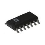
| 描述 | IC OPAMP JFET 8MHZ 14SOIC精密放大器 Lo Noise-Inpt Bias Crnt Wide BW JFET QD |
| 产品分类 | Linear - Amplifiers - Instrumentation, OP Amps, Buffer Amps集成电路 - IC |
| 品牌 | Analog Devices |
| 产品手册 | |
| 产品图片 |
|
| rohs | 符合RoHS无铅 / 符合限制有害物质指令(RoHS)规范要求 |
| 产品系列 | 放大器 IC,精密放大器,Analog Devices AD8513ARZ- |
| 数据手册 | |
| 产品型号 | AD8513ARZ |
| 产品培训模块 | http://www.digikey.cn/PTM/IndividualPTM.page?site=cn&lang=zhs&ptm=30008http://www.digikey.cn/PTM/IndividualPTM.page?site=cn&lang=zhs&ptm=26202 |
| 产品目录页面 | |
| 产品种类 | 精密放大器 |
| 供应商器件封装 | 14-SOIC |
| 共模抑制比—最小值 | 108 dB |
| 关闭 | No |
| 包装 | 管件 |
| 压摆率 | 20 V/µs |
| 双重电源电压 | 5 V to 15 V |
| 商标 | Analog Devices |
| 增益带宽生成 | 8 MHz |
| 增益带宽积 | 8MHz |
| 安装类型 | 表面贴装 |
| 安装风格 | SMD/SMT |
| 封装 | Tube |
| 封装/外壳 | 14-SOIC(0.154",3.90mm 宽) |
| 封装/箱体 | SOIC-14 |
| 工作温度 | -40°C ~ 125°C |
| 工作电源电压 | 5 V to 15 V |
| 工厂包装数量 | 56 |
| 放大器类型 | J-FET |
| 最大双重电源电压 | 15 V |
| 最大工作温度 | + 125 C |
| 最小双重电源电压 | 5 V |
| 最小工作温度 | - 40 C |
| 标准包装 | 56 |
| 电压-电源,单/双 (±) | ±4.5 V ~ 18 V |
| 电压-输入失调 | 100µV |
| 电压增益dB | 100.59 dB |
| 电流-电源 | 2.2mA |
| 电流-输入偏置 | 25pA |
| 电流-输出/通道 | 70mA |
| 电源电压-最大 | 5 V |
| 电源电压-最小 | 15 V |
| 电源电流 | 2.2 mA |
| 电源类型 | Dual |
| 电路数 | 4 |
| 系列 | AD8513 |
| 视频文件 | http://www.digikey.cn/classic/video.aspx?PlayerID=1364138032001&width=640&height=505&videoID=2245193153001http://www.digikey.cn/classic/video.aspx?PlayerID=1364138032001&width=640&height=505&videoID=2245193159001 |
| 转换速度 | 20 V/us |
| 输入偏压电流—最大 | 80 pA |
| 输入电压范围—最大 | 13 V |
| 输入补偿电压 | 0.1 mV |
| 输出电流 | 70 mA |
| 输出类型 | No |
| 通道数量 | 4 Channel |


- 商务部:美国ITC正式对集成电路等产品启动337调查
- 曝三星4nm工艺存在良率问题 高通将骁龙8 Gen1或转产台积电
- 太阳诱电将投资9.5亿元在常州建新厂生产MLCC 预计2023年完工
- 英特尔发布欧洲新工厂建设计划 深化IDM 2.0 战略
- 台积电先进制程称霸业界 有大客户加持明年业绩稳了
- 达到5530亿美元!SIA预计今年全球半导体销售额将创下新高
- 英特尔拟将自动驾驶子公司Mobileye上市 估值或超500亿美元
- 三星加码芯片和SET,合并消费电子和移动部门,撤换高东真等 CEO
- 三星电子宣布重大人事变动 还合并消费电子和移动部门
- 海关总署:前11个月进口集成电路产品价值2.52万亿元 增长14.8%


PDF Datasheet 数据手册内容提取
Precision, Very Low Noise, Low Input Bias Current, Wide Bandwidth JFET Operational Amplifiers Date Sheet AD8510/AD8512/AD8513 FEATURES PIN CONFIGURATIONS Fast settling time: 500 ns to 0.1% Low offset voltage: 400 μV maximum NULL 1 8 NC NULL 1 8 NC –IN 2 AD8510 7 V+ –IN 2 AD8510 7 V+ Low T V : 1 μV/°C typical C OS +IN 3 TOP VIEW 6 OUT +IN 3 TOP VIEW 6 OUT Low input bias current: 25 pA typical at V = ±15 V (Not to Scale) (Not to Scale) DLouwal n-souipsep:l 8y onpVe/√raHtzio tny:p ±ic5a Vl a tto f ± =1 15 kVH z S V– N4C = NO CONNECT5 NULL 02729-003 V– N4C = NO CONNECT5 NULL 02729-004 Figure 1. 8-Lead MSOP (RM Suffix) Figure 2. 8-Lead SOIC_N (R Suffix) Low distortion: 0.0005% No phase reversal Unity-gain stable OUT A 1 8 V+ OUT A 1 8 V+ –IN A 2 AD8512 7 OUT B –IN A 2 AD8512 7 OUT B AInPstPruLmICeAntTaItOioNn S +INV A– 34 (NToOt Pto V SIEcWale) 65 –+IINN BB 02729-001 +INV A– 34 (NToOt Pto V SIEcWale) 56 –+IINN BB 02729-002 Multipole filters Figure 3. 8-Lead MSOP (RM Suffix) Figure 4. 8-Lead SOIC_N (R Suffix) Precision current measurement Photodiode amplifiers OUT A 1 14 OUT D OUT A 1 14 OUT D Sensors –IN A 2 13 –IN D –IN A 2 13 –IN D Audio +IN A 3 AD8513 12 +IN D +IN A 3 AD8513 12 +IN D V+ 4 TOP VIEW 11 V– V+ 4 TOP VIEW 11 V– +IN B 5 (Not to Scale) 10 +IN C +IN B 5 (Not to Scale) 10 +IN C –IN B 6 9 –IN C –IN B 6 9 –IN C OUT B 7 8 OUT C 02729-005 OUT B 7 8 OUT C 02729-006 Figure 5. 14-Lead SOIC_N (R Suffix) Figure 6. 14-Lead TSSOP (RU Suffix) GENERAL DESCRIPTION The AD8510/AD8512/AD8513 are single-, dual-, and quad- Fast slew rate and great stability with capacitive loads make the precision JFET amplifiers that feature low offset voltage, input AD8510/AD8512/AD8513 a perfect fit for high performance bias current, input voltage noise, and input current noise. filters. Low input bias currents, low offset, and low noise result in a wide dynamic range of photodiode amplifier circuits. Low The combination of low offsets, low noise, and very low input noise and distortion, high output current, and excellent speed bias currents makes these amplifiers especially suitable for high make the AD8510/AD8512/AD8513 great choices for audio impedance sensor amplification and precise current measurements applications. using shunts. The combination of dc precision, low noise, and fast settling time results in superior accuracy in medical The AD8510/AD8512 are both available in 8-lead narrow SOIC_N instruments, electronic measurement, and automated test and 8-lead MSOP packages. MSOP-packaged devices are only equipment. Unlike many competitive amplifiers, the AD8510/ available in tape and reel. The AD8513 is available in 14-lead AD8512/AD8513 maintain their fast settling performance even SOIC_N and TSSOP packages. with substantial capacitive loads. Unlike many older JFET The AD8510/AD8512/AD8513 are specified over the −40°C to amplifiers, the AD8510/AD8512/AD8513 do not suffer from +125°C extended industrial temperature range. output phase reversal when input voltages exceed the maximum common-mode voltage range. Rev. K Document Feedback Information furnished by Analog Devices is believed to be accurate and reliable. However, no responsibility is assumed by Analog Devices for its use, nor for any infringements of patents or other One Technology Way, P.O. Box 9106, Norwood, MA 02062-9106, U.S.A. rights of third parties that may result from its use. Specifications subject to change without notice. No license is granted by implication or otherwise under any patent or patent rights of Analog Devices. Tel: 781.329.4700 ©2002–2018 Analog Devices, Inc. All rights reserved. Trademarks and registered trademarks are the property of their respective owners. Technical Support www.analog.com
AD8510/AD8512/AD8513 Date Sheet TABLE OF CONTENTS Features .............................................................................................. 1 Output Phase Reversal ............................................................... 14 Applications ....................................................................................... 1 Total Harmonic Distortion (THD) + Noise .............................. 14 Pin Configurations ........................................................................... 1 Total Noise Including Source Resistors ................................... 14 General Description ......................................................................... 1 Settling Time ............................................................................... 15 Revision History ............................................................................... 2 Overload Recovery Time .......................................................... 15 Specifications ..................................................................................... 4 Capacitive Load Drive ............................................................... 15 Electrical Characteristics ............................................................. 5 Open-Loop Gain and Phase Response .................................... 16 Absolute Maximum Ratings ............................................................ 7 Precision Rectifiers ..................................................................... 17 ESD Caution .................................................................................. 7 I-V Conversion Applications .................................................... 18 Typical Performance Characteristics ............................................. 8 Outline Dimensions ....................................................................... 20 General Application Information ................................................. 14 Ordering Guide .......................................................................... 21 Input Overvoltage Protection ................................................... 14 REVISION HISTORY 12/2018—Rev. J to Rev. K 6/2004—Rev. D to Rev. E Change to 8-Lead SOIC_N (R) Parameter, Table 4 ..................... 7 Changes to Format ............................................................. Universal Changes to Specifications ................................................................. 3 6/2017—Rev. I to Rev. J Updated Outline Dimensions ....................................................... 19 Changes to Figure 14 Caption ......................................................... 8 Deleted Figure 39; Renumbered Sequentially ............................ 12 10/2003—Rev. C to Rev. D Updated Outline Dimensions ....................................................... 19 Added AD8513 Model ....................................................... Universal Changes to Ordering Guide .......................................................... 20 Changes to Specifications ................................................................. 3 Added Figure 36 through Figure 40 ............................................. 10 2/2009—Rev. H to Rev. I Added Figure 55 and Figure 57 .................................................... 17 Changes to Figure 25 ...................................................................... 10 Changes to Ordering Guide .......................................................... 20 Changes to Ordering Guide .......................................................... 20 9/2003—Rev. B to Rev. C 10/2007—Rev. G to Rev. H Changes to Ordering Guide ............................................................ 4 Changes to Crosstalk Section ........................................................ 18 Updated Figure 2 ............................................................................ 10 Added Figure 58 .............................................................................. 18 Changes to Input Overvoltage Protection Section .................... 10 Changes to Figure 10 and Figure 11............................................. 12 6/2007—Rev. F to Rev. G Changes to Photodiode Circuits Section .................................... 13 Changes to Figure 1 and Figure 2 ................................................... 1 Changes to Figure 13 and Figure 14............................................. 13 Changes to Table 1 and Table 2 ....................................................... 3 Deleted Precision Current Monitoring Section ......................... 14 Updated Outline Dimensions ....................................................... 19 Updated Outline Dimensions ....................................................... 15 Changes to Ordering Guide .......................................................... 20 6/2006—Rev. E to Rev. F 3/2003—Rev. A to Rev. B Changes to Figure 23 ........................................................................ 9 Updated Figure 5 ............................................................................ 11 Updated Outline Dimensions ....................................................... 19 Updated Outline Dimensions ....................................................... 15 Changes to Ordering Guide .......................................................... 20 Rev. K | Page 2 of 21
Date Sheet AD8510/AD8512/AD8513 8/2002—Rev. 0 to Rev. A Added AD8510 Model ....................................................... Universal Added Pin Configurations ............................................................... 1 Changes to Specifications ................................................................. 2 Changes to Ordering Guide ............................................................. 4 Changes to TPC 2 and TPC 3 .......................................................... 5 Added TPC 10 and TPC 12 ............................................................. 6 Replaced TPC 20 ............................................................................... 8 Replaced TPC 27 ............................................................................... 9 Changes to General Application Information Section ............... 10 Changes to Figure 5 ......................................................................... 11 Changes to I-V Conversion Applications Section ...................... 13 Changes to Figure 13 and Figure 14 ............................................. 13 Changes to Figure 17 ...................................................................... 14 Rev. K | Page 3 of 21
AD8510/AD8512/AD8513 Date Sheet SPECIFICATIONS At V = ±5 V, V = 0 V, T = 25°C, unless otherwise noted. S CM A Table 1. Parameter Symbol Conditions Min Typ Max Unit INPUT CHARACTERISTICS Offset Voltage (B Grade)1 V 0.08 0.4 mV OS −40°C < T < +125°C 0.8 mV A Offset Voltage (A Grade) V 0.1 0.9 mV OS −40°C < T < +125°C 1.8 mV A Input Bias Current I 21 75 pA B −40°C < T < +85°C 0.7 nA A −40°C < T < +125°C 7.5 nA A Input Offset Current I 5 50 pA OS −40°C < T < +85°C 0.3 nA A −40°C < T < +125°C 0.5 nA A Input Capacitance Differential 12.5 pF Common Mode 11.5 pF Input Voltage Range −2.0 +2.5 V Common-Mode Rejection Ratio CMRR V = −2.0 V to +2.5 V 86 100 dB CM Large-Signal Voltage Gain A R = 2 kΩ, V = −3 V to +3 V 65 107 V/mV VO L O Offset Voltage Drift (B Grade)1 ΔV /ΔT 0.9 5 μV/°C OS Offset Voltage Drift (A Grade) ΔV /ΔT 1.7 12 μV/°C OS OUTPUT CHARACTERISTICS Output Voltage High V R = 10 kΩ 4.1 4.3 V OH L Output Voltage Low V R = 10 kΩ, −40°C < T < +125°C −4.9 −4.7 V OL L A Output Voltage High V R = 2 kΩ 3.9 4.2 V OH L Output Voltage Low V R = 2 kΩ, −40°C < T < +125°C −4.9 −4.5 V OL L A Output Voltage High V R = 600 Ω 3.7 4.1 V OH L Output Voltage Low V R = 600 Ω, −40°C < T < +125°C −4.8 −4.2 V OL L A Output Current I ±40 ±54 mA OUT POWER SUPPLY Power Supply Rejection Ratio PSRR V = ±4.5 V to ±18 V 86 130 dB S Supply Current/Amplifier I SY AD8510/AD8512/AD8513 V = 0 V 2.0 2.3 mA O AD8510/AD8512 −40°C < T < +125°C 2.5 mA A AD8513 −40°C < T < +125°C 2.75 mA A DYNAMIC PERFORMANCE Slew Rate SR R = 2 kΩ 20 V/μs L Gain Bandwidth Product GBP 8 MHz Settling Time t To 0.1%, 0 V to 4 V step, G = +1 0.4 μs S Total Harmonic Distortion (THD) + Noise THD + N 1 kHz, G = +1, R = 2 kΩ 0.0005 % L Phase Margin φ 44.5 Degrees M NOISE PERFORMANCE Voltage Noise Density e f = 10 Hz 34 nV/√Hz n f = 100 Hz 12 nV/√Hz f = 1 kHz 8.0 10 nV/√Hz f = 10 kHz 7.6 nV/√Hz Peak-to-Peak Voltage Noise e p-p 0.1 Hz to 10 Hz bandwidth 2.4 5.2 μV p-p n 1 AD8510/AD8512 only. Rev. K | Page 4 of 21
Date Sheet AD8510/AD8512/AD8513 ELECTRICAL CHARACTERISTICS At V = ±15 V, V = 0 V, T = 25°C, unless otherwise noted. S CM A Table 2. Parameter Symbol Conditions Min Typ Max Unit INPUT CHARACTERISTICS Offset Voltage (B Grade)1 V 0.08 0.4 mV OS −40°C < T < +125°C 0.8 mV A Offset Voltage (A Grade) V 0.1 1.0 mV OS −40°C < T < +125°C 1.8 mV A Input Bias Current I 25 80 pA B −40°C < T < +85°C 0.7 nA A −40°C < T < +125°C 10 nA A Input Offset Current I 6 75 pA OS −40°C < T < +85°C 0.3 nA A −40°C < T < +125°C 0.5 nA A Input Capacitance Differential 12.5 pF Common Mode 11.5 pF Input Voltage Range −13.5 +13.0 V Common-Mode Rejection Ratio CMRR V = −12.5 V to +12.5 V 86 108 dB CM Large-Signal Voltage Gain A R = 2 kΩ, V = 0 V, 115 196 V/mV VO L CM V = −13.5 V to +13.5 V O Offset Voltage Drift (B Grade)1 ΔV /ΔT 1.0 5 μV/°C OS Offset Voltage Drift (A Grade) ΔV /ΔT 1.7 12 μV/°C OS OUTPUT CHARACTERISTICS Output Voltage High V R = 10 kΩ +14.0 +14.2 V OH L Output Voltage Low V R = 10 kΩ, −40°C < T < +125°C −14.9 −14.6 V OL L A Output Voltage High V R = 2 kΩ +13.8 +14.1 V OH L Output Voltage Low V R = 2 kΩ, −40°C < T < +125°C –14.8 −14.5 V OL L A Output Voltage High V R = 600 Ω +13.5 +13.9 V OH L R = 600 Ω, −40°C < T < +125°C +11.4 V L A Output Voltage Low V R = 600 Ω −14.3 −13.8 V OL L R = 600 Ω, −40°C < T < +125°C −12.1 V L A Output Current I ±70 mA OUT POWER SUPPLY Power Supply Rejection Ratio PSRR V = ±4.5 V to ±18 V 86 dB S Supply Current/Amplifier I SY AD8510/AD8512/AD8513 V = 0 V 2.2 2.5 mA O AD8510/AD8512 −40°C < T < +125°C 2.6 mA A AD8513 −40°C < T < +125°C 3.0 mA A DYNAMIC PERFORMANCE Slew Rate SR R = 2 kΩ 20 V/μs L Gain Bandwidth Product GBP 8 MHz Settling Time t To 0.1%, 0 V to 10 V step, G = +1 0.5 μs S To 0.01%, 0 V to 10 V step, G = +1 0.9 μs Total Harmonic Distortion (THD) + Noise THD + N 1 kHz, G = +1, R = 2 kΩ 0.0005 % L Phase Margin φ 52 Degrees M Rev. K | Page 5 of 21
AD8510/AD8512/AD8513 Date Sheet Parameter Symbol Conditions Min Typ Max Unit NOISE PERFORMANCE Voltage Noise Density e f = 10 Hz 34 nV/√Hz n f = 100 Hz 12 nV/√Hz f = 1 kHz 8.0 10 nV/√Hz f = 10 kHz 7.6 nV/√Hz Peak-to-Peak Voltage Noise e p-p 0.1 Hz to 10 Hz bandwidth 2.4 5.2 μV p-p n 1 AD8510/AD8512 only. Rev. K | Page 6 of 21
Date Sheet AD8510/AD8512/AD8513 ABSOLUTE MAXIMUM RATINGS Table 4. Thermal Resistance Table 3. Package Type θ 1 θ Unit Parameter Rating JA JC 8-Lead MSOP (RM) 210 45 °C/W Supply Voltage ±18 V 8-Lead SOIC_N (R) 120 43 °C/W Input Voltage ±V S 14-Lead SOIC_N (R) 120 36 °C/W Output Short-Circuit Duration to GND Observe derating curves 14-Lead TSSOP (RU) 180 35 °C/W Storage Temperature Range −65°C to +150°C Operating Temperature Range −40°C to +125°C 1 θJA is specified for worst case conditions, that is, θJA is specified for device Junction Temperature Range −65°C to +150°C soldered in circuit board for surface-mount packages. Lead Temperature (Soldering, 10 sec) 300°C Electrostatic Discharge 2000 V ESD CAUTION (Human Body Model) Stresses at or above those listed under Absolute Maximum Ratings may cause permanent damage to the product. This is a stress rating only; functional operation of the product at these or any other conditions above those indicated in the operational section of this specification is not implied. Operation beyond the maximum operating conditions for extended periods may affect product reliability. Rev. K | Page 7 of 21
AD8510/AD8512/AD8513 Date Sheet TYPICAL PERFORMANCE CHARACTERISTICS 120 100k VSY = ±15V VSY = ±5V, ±15V TA = 25°C 100 RS A) 10k LIFIE 80 NT (p MP RE 1k A R F 60 U O C NUMBER 40 PUT BIAS 100 N I 20 10 0 –0.5 –0.4 –0.3 –0.2 –0.1 0 0.1 0.2 0.3 0.4 0.5 02729-007 1 02729-010 –40 –25 –10 5 20 35 50 65 80 95 110 125 INPUT OFFSET VOLTAGE (mV) TEMPERATURE (°C) Figure 7. Input Offset Voltage Distribution Figure 10. Input Bias Current vs. Temperature 30 1000 VSY = ±15V B GRADE 25 OFAMPLIFIERS 1250 ET CURRENT (pA)10100 ±15V UMBER 10 T OFFS ±5V N U P 1 N 5 I 0 02729-008 0.1 02729-011 0 1 2 3 4 5 6 –40 –25 –10 5 20 35 50 65 80 95 110 125 TCVOS (µV/°C) TEMPERATURE (°C) Figure 8. AD8510/AD8512 TCVOS Distribution Figure 11. Input Offset Current vs. Temperature 30 40 VSY = ±15V TA = 25°C A GRADE 35 25 RS A) 30 E p LIFI20 NT (25 P E M R MBER OFA1105 T BIAS CUR2105 U U N P10 N I 5 0 02729-009 508 13 18 23 28 3002729-012 0 1 2 3 4 5 6 TCVOS (µV/°C) SUPPLY VOLTAGE (V+ – V– ) Figure 9. AD8510/AD8512 TCVOS Distribution Figure 12. Input Bias Current vs. Supply Voltage Rev. K | Page 8 of 21
Date Sheet AD8510/AD8512/AD8513 2.0 2.8 mA) 1.9 TA = 25°C 2.6 TA = 25°C R ( 1.8 E 2.4 AMPLIFI 11..67 NT (mA) 2.2 ER RE 2.0 P 1.5 R NT CU 1.8 RE 1.4 LY R P CU 1.3 UP 1.6 Y S PL 1.2 1.4 P SU 11..01 02729-013 11..02 02729-016 8 13 18 23 28 30 8 13 18 23 28 33 SUPPLY VOLTAGE (V+ – V–) SUPPLY VOLTAGE (V+ – V–) Figure 13. AD8512 Supply Current per Amplifier vs. Supply Voltage Figure 16. AD8510 Supply Current vs. Supply Voltage 16 70 315 14 VOL VSY = ±15V 60 VCRSSLY C= O= 2P .±E51 k=5Ω V20pF 270 VOH 50 ΦM = 52° 225 12 V) 40 180 E ( s) OUTPUT VOLTAG1086 VOL VSY = ±5V GAIN (dB)1230000 41905305PHASE (Degree 4 VOH –10 –45 02 02729-039 ––3200 ––91035 02729-017 0 10 20 30 40 50 60 70 80 10k 100k 1M 10M 50M LOAD CURRENT (mA) FREQUENCY (Hz) Figure 14. Output Voltage vs. Load Current Figure 17. Open-Loop Gain and Phase vs. Frequency 2.50 2.50 A) m R (2.25 2.25 ±15V E AMPLIFI2.00 ±15V NT (mA)2.00 ±5V R E E R T P1.75 UR1.75 N ±5V C RE LY UR1.50 PP1.50 C U Y S L P SUP11..0205 02729-015 11..0205 02729-018 –40 –25 –10 5 20 35 50 65 80 95 110 125 –40 –25 –10 5 20 35 50 65 80 95 110 125 TEMPERATURE (°C) TEMPERATURE (°C) Figure 15. AD8512 Supply Current per Amplifier vs. Temperature Figure 18. AD8510 Supply Current vs. Temperature Rev. K | Page 9 of 21
AD8510/AD8512/AD8513 Date Sheet 70 300 VSY = ±15V 60 VSY = ±15V,±5V 270 VIN = 50mV 50 240 GAIN (dB) 3400 AV = 100 ANCE (Ω)128100 OOP 20 MPED150 AV = 1 CLOSED-L 100 AAVV == 110 OUTPUT I1269000 AV = 100 –10 AV = 10 ––3200 02729-019 300 02729-022 1k 10k 100k 1M 10M 50M 100 1k 10k 100k 1M 10M 100M FREQUENCY (Hz) FREQUENCY (Hz) Figure 19. Closed-Loop Gain vs. Frequency Figure 22. Output Impedance vs. Frequency 120 1k VSY = ±5V TO ±15V VSY = ±15V 100 Hz) V/ n 80 TY (100 B) NSI RR (d 60 E DE CM OIS N 40 E 10 G A T L O 20 V 0 02729-020 1 02729-023 100 1k 10k 100k 1M 10M 100M 1 10 100 1k 10k FREQUENCY (Hz) FREQUENCY (Hz) Figure 20. CMRR vs. Frequency Figure 23. Voltage Noise Density vs. Frequency 120 VSY = ±5V, ±15V VSY = ±15V 100 80 V) –PSRR DI V/ R (dB) 60 GE (1µ PSR 40 LTA O +PSRR V 20 –200 02729-021 02729-024 100 1k 10k 100k 1M 10M 100M TIME (1s/DIV) FREQUENCY (Hz) Figure 21. PSRR vs. Frequency Figure 24. 0.1 Hz to 10 Hz Input Voltage Noise Rev. K | Page 10 of 21
Date Sheet AD8510/AD8512/AD8513 280 90 VSY = ±5VTO ±15V VSY = ±15V 245 80 RL = 2kΩ Hz) %) V 210 T ( 70 n O OISE DENSITY (117450 NAL OVERSHO 456000 +OS–OS N105 G E SI 30 VOLTAG 70 SMALL- 20 350 02729-025 100 02729-028 0 1 2 3 4 5 6 7 8 9 10 1 10 100 1k 10k FREQUENCY (Hz) LOAD CAPACITANCE (pF) Figure 25. Voltage Noise Density vs. Frequency Figure 28. Small-Signal Overshoot vs. Load Capacitance 70 315 VSY = ±15V VSY = ±5V RL = 2kΩ 60 RL = 2.5kΩ 270 CL = 100pF CSCOPE = 20pF AV = 1 50 ΦM = 44.5° 225 DIV) N (dB) 40 180es) OLTAGE (5V/ N-LOOP GAI 231000 9140355HASE (Degre V E P OP 0 0 –10 –45 02729-026 ––2300 ––19305 02729-029 10k 100k 1M 10M 50M TIME (1µs/DIV) FREQUENCY (Hz) Figure 26. Large-Signal Transient Response Figure 29. Open-Loop Gain and Phase vs. Frequency 120 VSY = ±15V VSY = ±5V RL = 2kΩ 100 CL = 100pF AV = 1 V) 80 V/DI B) E (50m MRR (d 60 G C A LT 40 O V 20 02729-027 0100 1k 10k 100k 1M 10M 100M02729-030 TIME (100ns/DIV) FREQUENCY (Hz) Figure 27. Small-Signal Transient Response Figure 30. CMRR vs. Frequency Rev. K | Page 11 of 21
AD8510/AD8512/AD8513 Date Sheet 300 270 VVSINY == 5±05mVV VRCSLLY == = 21 k0±Ω05pVF 240 AV = 1 E (Ω)210 DIV) ANC180 AV= 1 mV/ PED150 E (50 M G UT I120 LTA TP AV= 100 VO U 90 O 60 300 AV= 10 02729-031 02729-034 100 1k 10k 100k 1M 10M 100M TIME (100ns/DIV) FREQUENCY (Hz) Figure 31. Output Impedance vs. Frequency Figure 34. Small-Signal Transient Response 100 VSY = ±5V VSY = ±5V 90 RL = 2kΩ %) T ( 80 O V) O 70 GE (1µV/DI L OVERSH 5600 +OS TA NA –OS VOL SIG 40 LL- 30 A M S 20 02729-032 100 02729-035 TIME (1s/DIV) 1 10 100 1k 10k LOAD CAPACITANCE (pF) Figure 32. 0.1 Hz to 10 Hz Input Voltage Noise Figure 35. Small-Signal Overshoot vs. Load Capacitance VSY = ±5V 100 RCLL == 21k0Ω0pF 90 VS = ±15V AV = 1 80 S R V) E 70 DI FI E (2V/ AMPLI 60 OLTAG ER OF 4500 V B M U 30 N 20 TIME (1µs/DIV) 02729-033 100 0 1 2 3 4 5 6 02729-036 TCVOS (µV/°C) Figure 33. Large-Signal Transient Response Figure 36. AD8513 TCVOS Distribution Rev. K | Page 12 of 21
Date Sheet AD8510/AD8512/AD8513 120 3.0 VS = ±5V A) 100 R (m 2.5 ±15V E PLIFIERS80 AMPLIFI 2.0 ±5V M R R OF A60 ENT PE 1.5 E R MB40 UR 1.0 U C N Y L P 20 P 0.5 0 02729-037 SU 0 02729-040 0 1 2 3 4 5 6 –40 –25 –10 5 20 35 50 65 80 95 110 125 TCVOS (µV/°C) TEMPERATURE (°C) Figure 37. AD8513 TCVOS Distribution Figure 39. AD8513 Supply Current per Amplifier vs. Temperature 2.5 TA= 25°C A)2.4 m R (2.3 E FI LI2.2 P M A2.1 R E P2.0 T N E1.9 R R CU1.8 Y PL1.7 P SU11..65 02729-038 8 13 18 23 28 33 SUPPLY VOLTAGE (V+ – V–) Figure 38. AD8513 Supply Current per Amplifier vs. Supply Voltage Rev. K | Page 13 of 21
AD8510/AD8512/AD8513 Date Sheet GENERAL APPLICATION INFORMATION INPUT OVERVOLTAGE PROTECTION 0.01 The AD8510/AD8512/AD8513 have internal protective VRSLY = = 1 0±05kVΩ circuitry that allows voltages as high as 0.7 V beyond the BW = 22kHz supplies to be applied at the input of either terminal without causing damage. For higher input voltages, a series resistor is %) necessary to limit the input current. The resistor value can be ON ( TI 0.001 determined from the formula R O T S V V DI IN S 5mA R S Wresiitsht oar v vearlyu elos wca onf fbsee tu csuerdr einn ts oerf i<es0 .w5 inthA t huep itnop 1u2t5s.° CA, 5h ikgΩh er 0.0001 02729-056 resistor protects the inputs from voltages as high as 25 V 20 100 1k 10k 20k FREQUENCY (Hz) beyond the supplies and adds less than 10 μV to the offset. Figure 41. THD + N vs. Frequency OUTPUT PHASE REVERSAL TOTAL NOISE INCLUDING SOURCE RESISTORS Phase reversal is a change of polarity in the transfer function of The low input current noise and input bias current of the the amplifier. This can occur when the voltage applied at the AD8510/AD8512/AD8513 make them the ideal amplifiers for input of an amplifier exceeds the maximum common-mode circuits with substantial input source resistance. Input offset voltage. voltage increases by less than 15 nV per 500 Ω of source Phase reversal can cause permanent damage to the device and resistance at room temperature. The total noise density of the can result in system lockups. The AD8510/AD8512/AD8513 do circuit is not exhibit phase reversal when input voltages are beyond the supplies. enTOTAL en2 inRS2 4kTRS where: VSY = ±5V e is the input voltage noise density of the devices. AV = 1 n RL = 10kΩ in is the input current noise density of the devices. R is the source resistance at the noninverting terminal. S V) VOUT k is Boltzmann’s constant (1.38 × 10⁻²³ J/K). DI V/ T is the ambient temperature in Kelvin (T = 273 + °C). 2 E ( G For R < 3.9 kΩ, e dominates and e ≈ e. The current noise A S n nTOTAL n LT VIN of the AD8510/AD8512/AD8513 is so low that its total density O V does not become a significant term unless R is greater than S 165 MΩ, an impractical value for most applications. 02729-057 Texhper etosstaedl e aqsu ivalent rms noise over a specific bandwidth is TIME (20µs/DIV) e e BW Figure 40. No Phase Reversal nTOTAL nTOTAL where BW is the bandwidth in hertz. TOTAL HARMONIC DISTORTION (THD) + NOISE Note that the previous analysis is valid for frequencies larger The AD8510/AD8512/AD8513 have low THD and excellent gain than 150 Hz and assumes flat noise above 10 kHz. For lower linearity, making these amplifiers great choices for precision frequencies, flicker noise (1/f) must be considered. circuits with high closed-loop gain and for audio application circuits. Figure 41 shows that the AD8510/AD8512/AD8513 have approximately 0.0005% of total distortion when configured in positive unity gain (the worst case) and driving a 100 kΩ load. Rev. K | Page 14 of 21
Date Sheet AD8510/AD8512/AD8513 SETTLING TIME VSY = ±15V Settling time is the time it takes the output of the amplifier to AV = –100 +15V RL = 10kΩ reach and remain within a percentage of its final value after a T U P pulse is applied at the input. The AD8510/AD8512/AD8513 T U O settle to within 0.01% in less than 900 ns with a step of 0 V to 0V E G 10 V in unity gain. This makes each of these devices an excellent A T L choice as a buffer at the output of DACs whose settling time is O V typically less than 1 μs. T 0V U P N In addition to the fast settling time and fast slew rate, low offset I–200mV voltage drift and input offset current maintain the full accuracy oOf V12E-RbiLt cOoAnvDer tRerEs CovOerV tEheR eYn tTirIeM opEe rating temperature range. 02729-054 TIME (2µs/DIV) Overload recovery, also known as overdrive recovery, is the Figure 43. Negative Overload Recovery time it takes the output of an amplifier to recover to its linear CAPACITIVE LOAD DRIVE region from a saturated condition. This recovery time is par- The AD8510/AD8512/AD8513 are unconditionally stable at all ticularly important in applications where the amplifier must gains in inverting and noninverting configurations. Each device amplify small signals in the presence of large transient voltages. is capable of driving a capacitive load of up to 1000 pF without Figure 42 shows the positive overload recovery of the AD8510/ oscillation in unity gain using the worst case configuration. AD8512/AD8513. The output recovers in approximately 200 ns However, as with most amplifiers, driving larger capacitive from a saturated condition. loads in a unity-gain configuration can cause excessive overshoot and ringing, or even oscillation. A simple snubber VSY = ±15V network significantly reduces the amount of overshoot and VIN = 200mV T 0V AV = –100 ringing. The advantage of this configuration is that the output UTPU RL = 10kΩ swing of the amplifier is not reduced, because RS is outside the O –15V feedback loop. E G A T L O V+ V T200mV U P N I 0V 2 7 02729-053 200mV 3 AD85104 6 RS VOUT Figure 42. PositiveT IOMvEe (r2lµosa/DdI RV)ecovery V– CS CL 02729-055 The negative overdrive recovery time shown in Figure 43 is less Figure 44. Snubber Network Configuration than 200 ns. In addition to the fast recovery time, the AD8510/AD8512/ AD8513 show excellent symmetry of the positive and negative recovery times. This is an important feature for transient signal rectification because the output signal is kept equally undistorted throughout any given period. Rev. K | Page 15 of 21
AD8510/AD8512/AD8513 Date Sheet Figure 45 shows a scope plot of the output of the AD8510/AD8512/ OPEN-LOOP GAIN AND PHASE RESPONSE AD8513 in response to a 400 mV pulse. The circuit is configured in In addition to their impressive low noise, low offset voltage, and positive unity gain (worst case) with a load experience of 500 pF. offset current, the AD8510/AD8512/AD8513 have excellent loop gain and phase response even when driving large resistive VSY = ±15V and capacitive loads. CL = 500pF RL =10kΩ Compared with Competitor A (see Figure 48) under the same V) conditions, with a 2.5 kΩ load at the output, the AD8510/AD8512/ DI V/ AD8513 have more than 8 MHz of bandwidth and a phase margin m 00 of more than 52°. 2 E ( G Competitor A, on the other hand, has only 4.5 MHz of band- A T OL width and 28° of phase margin under the same test conditions. V Even with a 1 nF capacitive load in parallel with the 2 kΩ load at the output, the AD8510/AD8512/AD8513 show much better 02729-041 rtoes lpeossn tshe atnh a0n, iCnodmicapteintigto ors Aci,l lwathioonse. phase margin is degraded TIME (1µs/DIV) Figure 45. Capacitive Load Drive Without Snubber 70 315 VSY = ±15V When the snubber circuit is used, the overshoot is reduced from 60 RL = 2.5kΩ 270 CL = 0pF 55% to less than 3% with the same load capacitance. Ringing is 50 225 virtually eliminated, as shown in Figure 46. 40 180 s) DIV) RVRCCSLLSSY ==== = 1511 00±0nk010Fp5ΩΩVF GAIN (dB)1230000 49105035PHASE (Degree V/ m –10 –45 0 0 LTAGE (2 ––320010k 100k 1M 10M 50M––19305 02729-043 O V FREQUENCY (Hz) Figure 47. Frequency Response of the AD8510/AD8512/AD8513 02729-042 70 315 TIME (1µs/DIV) 60 VRSLY = = 2 .±51k5ΩV 270 Figure 46. Capacitive Load with Snubber Network CL = 0pF 50 225 Optimum values for R and C depend on the load capacitance S S 40 180 and input stray capacitance and are determined empirically. s) TTaabbllee 55 s. hOopwtsim a ufemw Vvaalluueess t fhoart Ccaanp bacei utisveed L aosa sdtasr ting points. GAIN (dB) 123000 4915035ASE (Degree H CLOAD RS (Ω) CS 0 0 P 500 pF 100 1 nF –10 –45 2 nF 70 100 pF 5 nF 60 300 pF ––3200 ––91035 02729-044 10k 100k 1M 10M 50M FREQUENCY (Hz) Figure 48. Frequency Response of Competitor A Rev. K | Page 16 of 21
Date Sheet AD8510/AD8512/AD8513 PRECISION RECTIFIERS Rectifying circuits are used in a multitude of applications. One of the most popular uses is in the design of regulated power supplies, where a rectifier circuit is used to convert an input V) sinusoid to a unipolar output voltage. DI V/ 1 However, there are some potential problems with amplifiers E ( G used in this manner. When the input voltage (VIN) is negative, LTA the output is zero, and the magnitude of VIN is doubled at the VO inputs of the op amp. If this voltage exceeds the power supply voltage, it can permanently damage some amplifiers. In addition, tThhei so pd ealmayps tmheu sotu ctopmute s oigunt aolf b seactuaurastei othne w ahmepnl iVfiIeNr irse nqeugiraetisv e. 02729-046 time to enter its linear region. TIME (1ms/DIV) Figure 50. Half-Wave Rectifier Signal (OUT A in Figure 49) Although the AD8510/AD8512/AD8513 have a very fast overdrive recovery time, which makes them great choices for the rectification of transient signals, the symmetry of the positive and negative recovery times is also important to keep the output signal undistorted. V) DI Figure 49 shows the test circuit of the rectifier. The first stage of V/ 1 the circuit is a half-wave rectifier. When the sine wave applied at E ( G A the input is positive, the output follows the input response. LT O During the negative cycle of the input, the output tries to swing V negative to follow the input, but the power supply restrains it to zero. In a similar fashion, the second stage is a follower during tnheeg aptoivseit icvyec cley.c le of the sine wave and an inverter during the 02729-047 TIME (1ms/DIV) R2 R3 Figure 51. Full-Wave Rectifier Signal (OUT B in Figure 49) 10kΩ 10kΩ 10V 3VVIN p-p 6 2/2 4 3 1/2 8 AD8512 7 1Rk1Ω AD8512 1 5 8 O(FUUTL LBWAVE) 2 4 10V O(HUATL AFWAVE) 02729-045 Figure 49. Half-Wave and Full-Wave Rectifiers Rev. K | Page 17 of 21
AD8510/AD8512/AD8513 Date Sheet I-V CONVERSION APPLICATIONS A typical value for Rd is 1000 MΩ. Because Rd >> R2, the Photodiode Circuits circuit behavior is not impacted by the effect of the junction resistance. The maximum signal bandwidth is Common applications for I-V conversion include photodiode circuits where the amplifier is used to convert a current emitted ft f by a diode placed at the positive input terminal into an output MAX 2R2Ct voltage. where ft is the unity-gain frequency of the amplifier. The AD8510/AD8512/AD8513’s low input bias current, wide Cf can be calculated by bandwidth, and low noise make them each an excellent choice for various photodiode applications, including fax machines, Ct Cf fiber optic controls, motion sensors, and bar code readers. 2R2ft The circuit shown in Figure 52 uses a silicon diode with zero where ft is the unity-gain frequency of the op amp, and it achieves bias voltage. This is known as a photovoltaic mode; this a phase margin, φ , of approximately 45°. M configuration limits the overall noise and is suitable for A higher phase margin can be obtained by increasing the value instrumentation applications. of Cf. Setting Cf to twice the previous value yields approximately Cf φ = 65° and a maximal flat frequency response, but it reduces the M maximum signal bandwidth by 50%. R2 Using the previous parameters with a Cf ≈ 1 pF, the signal VEE bandwidth is approximately 2.6 MHz. Signal Transmission Applications 4 2 One popular signal transmission method uses pulse-width AD8510 6 modulation. High data rates can require a fast comparator Rd Ct 3 7 rather than an op amp. However, the need for sharp, undistorted VCC 02729-048 sTihgne aAlsD c8a5n1 f0a/vAoDr u8s5i1n2g/ Aa Dlin8e5a1r3 a mmapklief ieexr.c ellent voltage Figure 52. Equivalent Preamplifier Photodiode Circuit comparators. In addition to a high slew rate, the AD8510/ A larger signal bandwidth can be attained at the expense of AD8512/AD8513 have a very fast saturation recovery time. In additional output noise. The total input capacitance (Ct) the absence of feedback, the amplifiers are in open-loop mode consists of the sum of the diode capacitance (typically 3 pF to (very high gain). In this mode of operation, they spend much of 4 pF) and the amplifier’s input capacitance (12 pF), which their time in saturation. includes external parasitic capacitance. Ct creates a pole in the The circuit shown in Figure 53 was used to compare two signals frequency response that can lead to an unstable system. To of different frequencies, namely a 100 Hz sine wave and a 1 kHz ensure stability and optimize the bandwidth of the signal, a triangular wave. Figure 54 shows a scope plot of the resulting capacitor is placed in the feedback loop of the circuit shown in output waveforms. A pull-up resistor (typically 5 kΩ) can be Figure 52. It creates a zero and yields a bandwidth whose corner connected from the output to V if the output voltage needs to CC frequency is 1/(2π(R2Cf)). reach the positive rail. The trade-off is that power consumption The value of R2 can be determined by the ratio is higher. +15V V/I D where: 3 7 V is the desired output voltage of the op amp. 6 VOUT I is the diode current. D 2 4 For example, if I is 100 μA and a 10 V output voltage is desired, V1 D R2 can be 100 kΩ. Rd (see Figure 52) is a junction resistance ttehmatp derroaptus rtey.p ically by a factor of 2 for every 10°C increase in V2–15V 02729-049 Figure 53. Pulse-Width Modulator Rev. K | Page 18 of 21
Date Sheet AD8510/AD8512/AD8513 The AD8510 single has two additional active terminals that are not present on the AD8512 dual or AD8513 quad devices. These pins are labeled null and are used for fine adjustment of the input offset voltage. Although the guaranteed maximum offset V) voltage at room temperature is 400 μV and over the −40°C to DI V/ +125°C range is 800 mV maximum, this offset voltage can be 5 E ( reduced by adding a potentiometer to the null pins as shown in G A LT Figure 57. With the 20 kΩ potentiometer shown, the adjustment O V range is approximately ±3.5 mV. The potentiometer parallels low value resistors in the drain circuit of the JFET differential input pair and allows unbalancing of the drain currents to 02729-050 cthheasneg pei tnhse m ouffsste tb ev oleltfat guen. cIfo onfnfseectt eadd.j u stment is not required, TIME (2ms/DIV) Caution must be used when adding adjusting potentiometers to Figure 54. Pulse-Width Modulation any op amp with this capability for several reasons. First, there is Crosstalk gain from these nodes to the output; therefore, capacitive coupling Crosstalk, also known as channel separation, is a measure of from noisy traces to these nodes injects noise into the signal signal feedthrough from one channel to another on the same path. Second, the temperature coefficient of the potentiometer IC. The AD8512/AD8513 have a channel separation of better does not match the temperature coefficient of the internal resistors, than −90 dB for frequencies up to 10 kHz and of better than so the offset voltage drift with temperature is slightly affected. −50 dB for frequencies up to 10 MHz. Figure 56 shows the Third, this provision is for adjusting the offset voltage of the typical channel separation behavior between Amplifier A op amp, not for adjusting the offset of the overall system. Although (driving amplifier) and each of the following: Amplifier B, it is tempting to decrease the value of the potentiometer to attain Amplifier C, and Amplifier D. more range, this adversely affects the dc and ac parameters. Instead, increase the potentiometer to 50 kΩ to decrease the VOUT range if needed. 20kΩ 2.2kΩ 20kΩ +VS V+ 2 8 6 1 18V p-p 1 7 – 2 5 3 5 7 INPUT AD8510 6 OUTPUT 5kΩ 5kΩ 4 VIN + 3 CROSSTALK = 20 Floiggu1Vr0eOV U5ITN5. Crosstalk Tes–tV CSircuit 02729-052 V4– VTYOPS ITCRAILML RY A±N3.G5mE VIS 02729-058 Figure 57. Optional Offset Nulling Circuit 0 –20 dB) –40 N ( O TI –60 CH B A AR CH D CH C P –80 E S L E–100 N N A H–120 C ––116400 02729-051 100 1k 10k 100k 1M 10M FREQUENCY (Hz) Figure 56. Channel Separation Rev. K | Page 19 of 21
AD8510/AD8512/AD8513 Date Sheet OUTLINE DIMENSIONS 5.10 5.00(0.1968) 5.00 4.80(0.1890) 4.90 8 5 4.00 (0.1574) 6.20 (0.2441) 14 8 3.80 (0.1497) 1 4 5.80 (0.2284) 4.50 4.40 6.40 BSC 4.30 1.27 (0.0500) 0.50 (0.0196) BSC 1.75 (0.0688) 0.25 (0.0099) 45° 1 7 0.25 (0.0098) 1.35 (0.0532) 8° 0.10 (0.0040) 0° PIN 1 COPLANARITY 0.51 (0.0201) 1.05 0.65 0.10 SEPALTAINNGE 0.31 (0.0122) 00..2157 ((00..00009687)) 10..2470 ((00..00510507)) 10..0800 BSC 1M.A20X 00..2009 0.75 C(RINOEFNPETARRREOENNLCLTEIHN CEOGOSN MEDLSIPYM)LAEAIANNRNDSETI AORTRNOOESU JNANEORDDEETE DAICN-P O SMPFTRIFALO NLMPDIIMRLAELIRATIMDTEESER TFSMEO;S RIR-N 0 ECU1Q2HS-U EADI VAIINMA LEDENENSSTIIOGSN NFS.OR 012407-A 00..1055COM00..P3109LIANT SPTELOAA JNTEIENDGEC CSOTAPNL0AD.1NA0ARRDIST YMO80°°-153-AB-1 00..6405 Figure 58. 8-Lead Standard Small Outline Package [SOIC_N] Figure 60. 14-Lead Thin Shrink Small Outline Package [TSSOP] Narrow Body (R-8) (RU-14) Dimensions shown in millimeters and (inches) Dimensions shown in millimeters 3.20 3.00 2.80 8 5 5.15 8.75 (0.3445) 3.20 4.90 8.55 (0.3366) 3.00 4.65 2.80 1 4 4.00 (0.1575) 14 8 6.20 (0.2441) 3.80 (0.1496) 1 7 5.80 (0.2283) PIN 1 IDENTIFIER 0.65 BSC 1.27 B(0S.C0500) 1.75 (0.0689) 00..5205 ((00..00109978)) 45° 0.95 15° MAX 0.25 (0.0098) 1.35 (0.0531) 8° 0.85 1.10 MAX 0.10 (0.0039) 0° 0.75 COPL0A.1N0ARITY 0.51 (0.0201) SPELAATNIENG 0.25 (0.0098) 1.27 (0.0500) 0.15 0.40 6° 0.23 00..8505 0.31 (0.0122) 0.17 (0.0067) 0.40 (0.0157) CO0P.0L50A.1N0ARICTOYMPLIANT0. 2T5O JEDEC STA0°NDARDS 0M.0O9-187-AA 0.40 10-07-2009-B C(RINOEFNPEATRRREOENNLCLTEIHNC EOGOSN MEDLSIPYM)LAEAIANNRNDSETI AORTRNOOESU JNANEORDDEETE DAICN-P O SMPFTRIFALO NLMPDIIMRLAELIRATIMDTEESER TFMSEO;S RIR-N 0 ECU1Q2HS-U EADI VBIINMA LEDENENSSTIIOGSN NFS.OR 060606-A Figure 59. 8-Lead Mini Small Outline Package [MSOP] Figure 61. 14-Lead Standard Small Outline Package [SOIC_N] (RM-8) Narrow Body (R-14) Dimensions shown in millimeters Dimensions shown in millimeters and (inches) Rev. K | Page 20 of 21
Date Sheet AD8510/AD8512/AD8513 ORDERING GUIDE Model1 Temperature Range Package Description Package Option Marking Code AD8510ARMZ-REEL −40°C to +125°C 8-Lead MSOP RM-8 B7A# AD8510ARMZ −40°C to +125°C 8-Lead MSOP RM-8 B7A# AD8510ARZ −40°C to +125°C 8-Lead SOIC_N R-8 AD8510ARZ-REEL −40°C to +125°C 8-Lead SOIC_N R-8 AD8510ARZ-REEL7 −40°C to +125°C 8-Lead SOIC_N R-8 AD8510BRZ −40°C to +125°C 8-Lead SOIC_N R-8 AD8510BRZ-REEL −40°C to +125°C 8-Lead SOIC_N R-8 AD8510BRZ-REEL7 −40°C to +125°C 8-Lead SOIC_N R-8 AD8512ARMZ-REEL −40°C to +125°C 8-Lead MSOP RM-8 B8A# AD8512ARMZ −40°C to +125°C 8-Lead MSOP RM-8 B8A# AD8512ARZ −40°C to +125°C 8-Lead SOIC_N R-8 AD8512ARZ-REEL −40°C to +125°C 8-Lead SOIC_N R-8 AD8512ARZ-REEL7 −40°C to +125°C 8-Lead SOIC_N R-8 AD8512BRZ −40°C to +125°C 8-Lead SOIC_N R-8 AD8512BRZ-REEL −40°C to +125°C 8-Lead SOIC_N R-8 AD8512BRZ-REEL7 −40°C to +125°C 8-Lead SOIC_N R-8 AD8513ARZ −40°C to +125°C 14-Lead SOIC_N R-14 AD8513ARZ-REEL −40°C to +125°C 14-Lead SOIC_N R-14 AD8513ARZ-REEL7 −40°C to +125°C 14-Lead SOIC_N R-14 AD8513ARUZ −40°C to +125°C 14-Lead TSSOP RU-14 AD8513ARUZ-REEL −40°C to +125°C 14-Lead TSSOP RU-14 1 Z = RoHS Compliant Part, # denotes RoHS compliant product may be top or bottom marked. ©2002–2018 Analog Devices, Inc. All rights reserved. Trademarks and registered trademarks are the property of their respective owners. D02729-0-12/18(K) Rev. K | Page 21 of 21
Mouser Electronics Authorized Distributor Click to View Pricing, Inventory, Delivery & Lifecycle Information: A nalog Devices Inc.: AD8510ARMZ AD8510ARZ AD8512ARMZ AD8512ARZ AD8512BRZ AD8513ARUZ AD8513ARZ AD8510ARMZ- REEL AD8510ARZ-REEL AD8510ARZ-REEL7 AD8510BR-REEL AD8510BRZ AD8510BRZ-REEL AD8510BRZ- REEL7 AD8512ARMZ-REEL AD8512ARZ-REEL AD8512ARZ-REEL7 AD8512BR AD8512BR-REEL AD8512BR- REEL7 AD8512BRZ-REEL AD8512BRZ-REEL7 AD8513AR AD8513AR-REEL AD8513AR-REEL7 AD8513ARUZ- REEL AD8513ARZ-REEL AD8513ARZ-REEL7