ICGOO在线商城 > 集成电路(IC) > 线性 - 放大器 - 仪表,运算放大器,缓冲器放大器 > TLV341IDRLR
 Datasheet下载
- 型号: TLV341IDRLR
- 制造商: Texas Instruments
- 库位|库存: xxxx|xxxx
- 要求:
| 数量阶梯 | 香港交货 | 国内含税 |
| +xxxx | $xxxx | ¥xxxx |
查看当月历史价格
查看今年历史价格
TLV341IDRLR产品简介:
ICGOO电子元器件商城为您提供TLV341IDRLR由Texas Instruments设计生产,在icgoo商城现货销售,并且可以通过原厂、代理商等渠道进行代购。 TLV341IDRLR价格参考¥2.37-¥5.85。Texas InstrumentsTLV341IDRLR封装/规格:线性 - 放大器 - 仪表,运算放大器,缓冲器放大器, 通用 放大器 1 电路 满摆幅 6-SOT。您可以下载TLV341IDRLR参考资料、Datasheet数据手册功能说明书,资料中有TLV341IDRLR 详细功能的应用电路图电压和使用方法及教程。
TLV341IDRLR 是由 Texas Instruments(德州仪器)生产的一款低功耗、单通道运算放大器,属于线性放大器中的仪表、运算放大器和缓冲器放大器类别。其主要应用场景包括以下方面:

1. 便携式电子设备:
   TLV341IDRLR 的低静态电流(典型值为 280 µA)使其非常适合用于电池供电的便携式设备,例如手持式测量仪器、便携式医疗设备(如血糖仪或脉搏血氧仪)以及消费类电子产品。

2. 传感器信号调理:
   该运放具有高输入阻抗和低输入偏置电流,适合用于微弱信号的放大,例如温度传感器、压力传感器或光电二极管等输出信号的调理电路中。

3. 音频信号处理:
   TLV341IDRLR 可用作音频信号的前置放大器,适用于低功率音频系统,如耳机放大器或小型音响设备。

4. 工业自动化与控制:
   在工业领域,该运放可用于数据采集系统的信号调理部分,例如将传感器信号转换为适合 ADC 输入的电平范围。

5. 医疗设备:
   其低噪声特性使其适合用于需要高精度信号放大的医疗设备,例如心电图(ECG)或脑电图(EEG)监测设备。

6. 通信设备:
   TLV341IDRLR 可用于低功耗通信设备中的信号放大和滤波,例如无线传感器节点或物联网(IoT)设备。

7. 汽车电子:
   在汽车应用中,该运放可用于车内传感器信号的放大和处理,例如胎压监测系统(TPMS)或环境传感器。

总之,TLV341IDRLR 凭借其低功耗、高精度和宽工作电压范围(1.8V 至 5.5V),广泛适用于需要高性能和低功耗的各种场景,特别是在对电源效率要求较高的应用中表现出色。
| 参数 | 数值 |
| -3db带宽 | - |
| 产品目录 | 集成电路 (IC)半导体 |
| 描述 | IC OPAMP GP 2.3MHZ RRO SOT23-6运算放大器 - 运放 Low-Voltage R-To-R Output CMOS |
| 产品分类 | Linear - Amplifiers - Instrumentation, OP Amps, Buffer Amps集成电路 - IC |
| 品牌 | Texas Instruments |
| 产品手册 | |
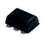
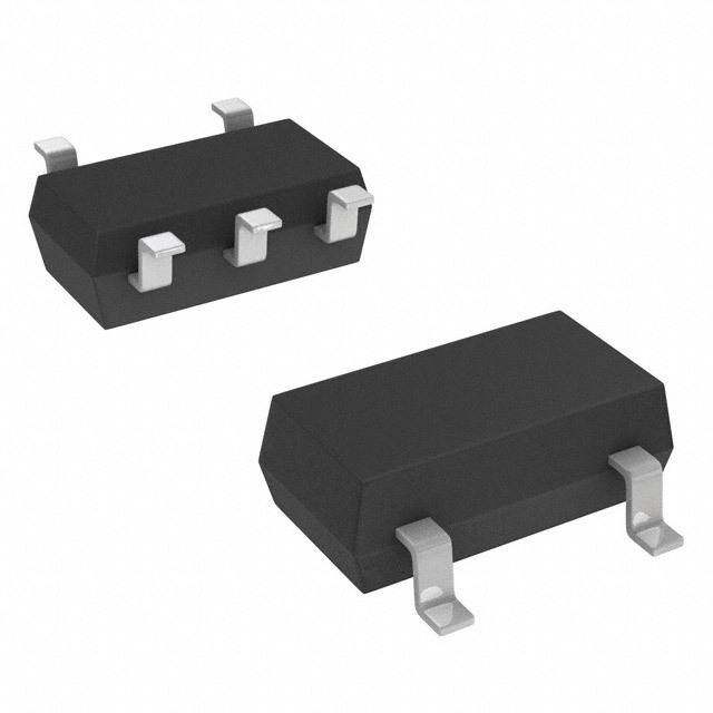
| 产品图片 |
|
| rohs | 符合RoHS无铅 / 符合限制有害物质指令(RoHS)规范要求 |
| 产品系列 | 放大器 IC,运算放大器 - 运放,Texas Instruments TLV341IDRLR- |
| 数据手册 | |
| 产品型号 | TLV341IDRLR |
| 产品种类 | 运算放大器 - 运放 |
| 供应商器件封装 | SOT-23-6 |
| 共模抑制比—最小值 | 75 dB |
| 关闭 | Shutdown |
| 其它名称 | 296-21126-1 |
| 包装 | 剪切带 (CT) |
| 单位重量 | 2.800 mg |
| 压摆率 | 1 V/µs |
| 商标 | Texas Instruments |
| 增益带宽生成 | 2.3 MHz |
| 增益带宽积 | 2.3MHz |
| 安装类型 | 表面贴装 |
| 安装风格 | SMD/SMT |
| 封装 | Reel |
| 封装/外壳 | SOT-563,SOT-666 |
| 封装/箱体 | SOT-553-6 |
| 工作温度 | -40°C ~ 125°C |
| 工作电源电压 | 1.5 V to 5.5 V |
| 工厂包装数量 | 4000 |
| 技术 | CMOS |
| 放大器类型 | 通用 |
| 最大工作温度 | + 125 C |
| 最小工作温度 | - 40 C |
| 标准包装 | 1 |
| 电压-电源,单/双 (±) | 1.5 V ~ 5.5 V |
| 电压-输入失调 | 300µV |
| 电流-电源 | 75µA |
| 电流-输入偏置 | 1pA |
| 电流-输出/通道 | 115mA |
| 电源电流 | 0.15 mA |
| 电路数 | 1 |
| 系列 | TLV341 |
| 转换速度 | 1 V/us |
| 输入偏压电流—最大 | 200 pA |
| 输入参考电压噪声 | 33 nV |
| 输入补偿电压 | 4 mV |
| 输出电流 | 115 mA |
| 输出类型 | 满摆幅 |
| 通道数量 | 1 Channel |


- 商务部:美国ITC正式对集成电路等产品启动337调查
- 曝三星4nm工艺存在良率问题 高通将骁龙8 Gen1或转产台积电
- 太阳诱电将投资9.5亿元在常州建新厂生产MLCC 预计2023年完工
- 英特尔发布欧洲新工厂建设计划 深化IDM 2.0 战略
- 台积电先进制程称霸业界 有大客户加持明年业绩稳了
- 达到5530亿美元!SIA预计今年全球半导体销售额将创下新高
- 英特尔拟将自动驾驶子公司Mobileye上市 估值或超500亿美元
- 三星加码芯片和SET,合并消费电子和移动部门,撤换高东真等 CEO
- 三星电子宣布重大人事变动 还合并消费电子和移动部门
- 海关总署:前11个月进口集成电路产品价值2.52万亿元 增长14.8%


PDF Datasheet 数据手册内容提取
Product Sample & Technical Tools & Support & Folder Buy Documents Software Community TLV341,TLV341A,TLV342,TLV342S SLVS568D–JANUARY2005–REVISEDAPRIL2016 TLV34xx Low-Voltage Rail-to-Rail Output CMOS Operational Amplifiers With Shutdown 1 Features 3 Description • 1.8-Vand5-VPerformance The TLV34xx devices are single and dual CMOS 1 operational amplifiers, respectively, with low-voltage, • LowOffset(AGrade) low-power, and rail-to-rail output swing capabilities. – 1.25mVMaximum(25°C) The PMOS input stage offers an ultra-low input bias – 1.7mVMaximum(–40°Cto125°C) currentof1pA(typical)andanoffsetvoltageof 0.3 mV (typical). For applications requiring excellent • Rail-to-RailOutputSwing dc precision, the A grade (TLV34xA) has a low offset • WideCommon-ModeInputVoltageRange:–0.2V voltageof1.25mV(maximum)at25°C. to(V –0.5V) + These single-supply amplifiers are designed • InputBiasCurrent:1pA(Typical) specifically for ultra-low-voltage (1.5 V to 5 V) • InputOffsetVoltage:0.3mV(Typical) operation, with a common-mode input voltage range • LowSupplyCurrent:70μA/Channel that typically extends from –0.2 V to 0.5 V from the positivesupplyrail. • LowShutdownCurrent: 10pA(Typical)PerChannel The TLV341 (single) and TLV342 (dual) in the RUG • GainBandwidth:2.3MHz(Typical) package also offer a shutdown (SHDN) pin that can be used to disable the device. In shutdown mode, the • SlewRate:0.9V/μs(Typical) supply current is reduced to 45 pA (typical). Offered • TurnonTimeFromShutdown:5 μs(Typical) in both the SOT-23 and smaller SC70 packages, the • InputReferredVoltageNoise(at10kHz): TLV341 is suitable for the most space-constrained applications. The dual TLV342 is offered in the 20nV/√Hz standardSOIC,VSSOP,andX2QFNpackages. • ESDProtectionExceedsJESD22 An extended industrial temperature range from –40°C – 2000-VHuman-BodyModel(HBM) to 125°C makes the TLV34xx suitable in a wide – 750-VCharged-devicemodel(CDM) varietyofcommercialandindustrialapplications. 2 Applications DeviceInformation(1) • CellularPhones PARTNUMBER PACKAGE BODYSIZE(NOM) • ConsumerElectronics(Laptops) SOT-23(6) 2.90mm×1.60mm • AudioPreamplifierforVoice TLV341 SC70(6) 2.00mm×1.25mm • PortableandBattery-PoweredElectronic SOT(6) 1.60mm×1.20mm Equipment SOIC(8) 4.90mm×3.91mm • SupplyCurrentMonitoring TLV342 VSSOP(8) 3.00mm×3.00mm X2QFN(10) 1.50mm×2.00mm • BatteryMonitoring TLV342S X2QFN(10) 1.50mm×2.00mm • Buffers (1) For all available packages, see the orderable addendum at • Filters theendofthedatasheet. SampleandHoldCircuitUsingTwoTLV341 V+ V+ − − VO + VI + C = 200 pF Sample Clock Copyright © 2016,Texas Instruments Incorporated 1 An IMPORTANT NOTICE at the end of this data sheet addresses availability, warranty, changes, use in safety-critical applications, intellectualpropertymattersandotherimportantdisclaimers.PRODUCTIONDATA.
TLV341,TLV341A,TLV342,TLV342S SLVS568D–JANUARY2005–REVISEDAPRIL2016 www.ti.com Table of Contents 1 Features.................................................................. 1 7.1 Overview.................................................................15 2 Applications........................................................... 1 7.2 FunctionalBlockDiagram.......................................15 3 Description............................................................. 1 7.3 FeatureDescription.................................................15 7.4 DeviceFunctionalModes........................................15 4 RevisionHistory..................................................... 2 8 ApplicationandImplementation........................ 16 5 PinConfigurationandFunctions......................... 3 8.1 ApplicationInformation............................................16 6 Specifications......................................................... 4 8.2 TypicalApplication .................................................16 6.1 AbsoluteMaximumRatings......................................4 9 PowerSupplyRecommendations...................... 17 6.2 ESDRatings..............................................................4 10 Layout................................................................... 18 6.3 RecommendedOperatingConditions.......................5 6.4 ThermalInformation:TLV341...................................5 10.1 LayoutGuidelines.................................................18 6.5 ThermalInformation:TLV342...................................5 10.2 LayoutExample....................................................18 6.6 ThermalInformation:TLV342S.................................5 11 DeviceandDocumentationSupport................. 19 6.7 ElectricalCharacteristics:V =1.8V........................6 11.1 RelatedLinks........................................................19 + 6.8 ElectricalCharacteristics:V =5V...........................7 11.2 CommunityResource............................................19 + 6.9 ShutdownCharacteristics:V =1.8V.......................8 11.3 Trademarks...........................................................19 + 6.10 ShutdownCharacteristics:V =5V........................8 11.4 ElectrostaticDischargeCaution............................19 + 6.11 TypicalCharacteristics............................................9 11.5 Glossary................................................................19 7 DetailedDescription............................................ 15 12 Mechanical,Packaging,andOrderable Information........................................................... 19 4 Revision History NOTE:Pagenumbersforpreviousrevisionsmaydifferfrompagenumbersinthecurrentversion. ChangesfromRevisionC(November2007)toRevisionD Page • AddedESDRatingstable,FeatureDescriptionsection,DeviceFunctionalModes,ApplicationandImplementation section,PowerSupplyRecommendationssection,Layoutsection,DeviceandDocumentationSupportsection,and Mechanical,Packaging,andOrderableInformationsection ................................................................................................. 1 • RemovedDPKpackageandTLV344partfromthePinConfigurationandFunctionstable ................................................ 3 2 SubmitDocumentationFeedback Copyright©2005–2016,TexasInstrumentsIncorporated ProductFolderLinks:TLV341 TLV341A TLV342 TLV342S
TLV341,TLV341A,TLV342,TLV342S www.ti.com SLVS568D–JANUARY2005–REVISEDAPRIL2016 5 Pin Configuration and Functions TLV341DBVorDCKPackage 6-PinSOT-23orSC70 TLV341DRLPackage TopView 6-PinSOT TopView GINND+ 12 65 VS+HDN GND 1 6 V+ IN+ 2 5 SHDN IN− 3 4 OUT IN− 3 4 OUT PinFunctions:TLV341 PIN I/O DESCRIPTION NAME SOT-23,SC70 SOT 1IN+ 1 2 I Noninvertinginputonchannel1 1IN– 3 3 I Invertinginputonchannel1 1OUT 4 4 O Outputonchannel1 GND 2 1 — Ground SHDN 5 5 I Shutdownactivelow V 6 6 — Positivepowersupply + TLV342DorDGKPackage 10-PinSOICorVSSOP TLV342RUGPackage TopView 10-PinX2QFN TopView 1OUT 1 8 V+ 1IN− 1IN− 2 7 2OUT 1IN+ 1 10 9 1OUT 1IN+ 3 6 2IN− GND 2 8 NC GND 4 5 2IN+ NC 3 7 V+ 2IN+ 4 6 2OUT 5 2IN− PinFunctions:TLV342 PIN I/O DESCRIPTION NAME SOIC,VSSOP X2QFN 1IN+ 3 1 I Noninvertinginputonchannel1 1IN– 2 10 I Invertinginputonchannel1 1OUT 1 9 O Outputonchannel1 2IN+ 5 4 I Noninvertinginputonchannel2 2IN– 6 5 I Invertinginputonchannel2 2OUT 7 6 O Outputonchannel2 GND 4 2 — Ground NC(1) — 3,8 — Notconnected V 8 7 — Positivepowersupply + (1) NC–Nointernalconnection Copyright©2005–2016,TexasInstrumentsIncorporated SubmitDocumentationFeedback 3 ProductFolderLinks:TLV341 TLV341A TLV342 TLV342S
TLV341,TLV341A,TLV342,TLV342S SLVS568D–JANUARY2005–REVISEDAPRIL2016 www.ti.com TLV342SRUGPackage 10-PinX2QFN TopView 1IN− 1IN+ 1 10 9 1OUT GND 2 8 NC SHDN 3 7 V+ 2IN+ 4 6 2OUT 5 2IN− PinFunctions:TLV342S PIN I/O DESCRIPTION NAME NO. 1IN+ 1 I Noninvertinginputonchannel1 1IN– 10 I Invertinginputonchannel1 1OUT 9 O Outputonchannel1 2IN+ 4 I Noninvertinginputonchannel2 2IN– 5 I Invertinginputonchannel2 2OUT 6 O Outputonchannel2 GND 2 — Ground NC(1) 8 — Notconnected SHDN 3 I Shutdownactivelow V 7 — Positivepowersupply + (1) NC–Nointernalconnection 6 Specifications 6.1 Absolute Maximum Ratings overoperatingfree-airtemperaturerange(unlessotherwisenoted)(1) MIN MAX UNIT V Supplyvoltage(2) –0.3 5.5 V + V Differentialinputvoltage(3) ±5.5 V ID V Inputvoltage(eitherinputorshutdown) –0.3 5.5 V I V Outputvoltage –0.3 V +0.3 V O CC T Operatingvirtual-junctiontemperature 150 °C J T Storagetemperature –65 150 °C stg (1) StressesbeyondthoselistedunderAbsoluteMaximumRatingsmaycausepermanentdamagetothedevice.Thesearestressratings only,andfunctionaloperationofthedeviceattheseoranyotherconditionsbeyondthoseindicatedunderRecommendedOperating Conditionsisnotimplied.Exposuretoabsolute-maximum-ratedconditionsforextendedperiodsmayaffectdevicereliability. (2) Allvoltagevalues(exceptdifferentialvoltages)arewithrespecttothenetworkGND. (3) DifferentialvoltagesareatIN+withrespecttoIN−. 6.2 ESD Ratings VALUE UNIT Human-bodymodel(HBM),perANSI/ESDA/JEDECJS-001(1) ±2000 V Electrostaticdischarge V (ESD) Charged-devicemodel(CDM),perJEDECspecificationJESD22-C101(2) ±750 (1) JEDECdocumentJEP155statesthat500-VHBMallowssafemanufacturingwithastandardESDcontrolprocess. (2) JEDECdocumentJEP157statesthat250-VCDMallowssafemanufacturingwithastandardESDcontrolprocess. 4 SubmitDocumentationFeedback Copyright©2005–2016,TexasInstrumentsIncorporated ProductFolderLinks:TLV341 TLV341A TLV342 TLV342S
TLV341,TLV341A,TLV342,TLV342S www.ti.com SLVS568D–JANUARY2005–REVISEDAPRIL2016 6.3 Recommended Operating Conditions MIN MAX UNIT V Supplyvoltage(single-supplyoperation) 1.5 5.5 V + T Operatingfree-airtemperature –40 125 °C A 6.4 Thermal Information: TLV341 TLV341 THERMALMETRIC(1) DBV DCK DRL UNIT (SOT-23) (SC70) (SOT) 6PINS 6PINS 6PINS R Junction-to-ambientthermalresistance 193.4 196.8 221.1 °C/W θJA R Junction-to-case(top)thermalresistance 145.6 82.4 109.1 °C/W θJC(top) R Junction-to-boardthermalresistance 44.1 95.2 111.4 °C/W θJB ψ Junction-to-topcharacterizationparameter 34.1 1.8 6.2 °C/W JT ψ Junction-to-boardcharacterizationparameter 43.4 93.2 109.8 °C/W JB (1) Formoreinformationabouttraditionalandnewthermalmetrics,seetheSemiconductorandICPackageThermalMetricsapplication report,SPRA953. 6.5 Thermal Information: TLV342 TLV342 THERMALMETRIC(1) D DGK RUG UNIT (SOIC) (MSOP) (X2QFN) 8PINS 8PINS 10PINS R Junction-to-ambientthermalresistance 123.6 192.3 167 °C/W θJA R Junction-to-case(top)thermalresistance 69.8 78.2 56.5 °C/W θJC(top) R Junction-to-boardthermalresistance 63.9 112.6 94.3 °C/W θJB ψ Junction-to-topcharacterizationparameter 24.4 15.2 4.1 °C/W JT ψ Junction-to-boardcharacterizationparameter 63.4 111.2 94 °C/W JB (1) Formoreinformationabouttraditionalandnewthermalmetrics,seetheSemiconductorandICPackageThermalMetricsapplication report,SPRA953. 6.6 Thermal Information: TLV342S TLV342S THERMALMETRIC(1) RUG UNIT (X2QFN) 10PINS R Junction-to-ambientthermalresistance 158.3 °C/W θJA R Junction-to-case(top)thermalresistance 52.6 °C/W θJC(top) R Junction-to-boardthermalresistance 87.9 °C/W θJB ψ Junction-to-topcharacterizationparameter 1 °C/W JT ψ Junction-to-boardcharacterizationparameter 87 °C/W JB (1) Formoreinformationabouttraditionalandnewthermalmetrics,seetheSemiconductorandICPackageThermalMetricsapplication report,SPRA953. Copyright©2005–2016,TexasInstrumentsIncorporated SubmitDocumentationFeedback 5 ProductFolderLinks:TLV341 TLV341A TLV342 TLV342S
TLV341,TLV341A,TLV342,TLV342S SLVS568D–JANUARY2005–REVISEDAPRIL2016 www.ti.com 6.7 Electrical Characteristics: V = 1.8 V + V =1.8V,GND=0V,V =V =V /2,R >1MΩ(unlessotherwisenoted).SeeShutdownCharacteristics:V =1.8V. + IC O + L + PARAMETER TESTCONDITIONS T MIN TYP(1) MAX UNIT A 25°C 0.3 4 Standardgrade Fullrange 4.5 V Inputoffsetvoltage 25°C 0.3 1.25 mV IO Agrade 0°Cto125°C 0.3 1.5 –40°Cto125°C 0.3 1.7 Averagetemperaturecoefficient α Fullrange 1.9 μV/°C VIO ofinputoffsetvoltage 25°C 1 100 I Inputbiascurrent –40°Cto85°C 375 pA IB –40°Cto125°C 3000 I Inputoffsetcurrent 25°C 6.6 fA IO 25°C 60 85 CMRR Common-moderejectionratio 0≤V ≤1.2V dB ICR Fullrange 50 25°C 75 95 k Supply-voltagerejectionratio 1.8V≤V ≤5V dB SVR + Fullrange 65 Common-modeinputvoltage V CMRR≥60dB 25°C 0 1.2 V ICR range 25°C 70 110 R =10kΩto1.35V L Fullrange 60 A Large-signalvoltagegain(2) dB V 25°C 65 100 R =2kΩto1.35V L Fullrange 55 25°C 22 50 Lowlevel Fullrange 75 R =2kΩto1.35V L 25°C 25 50 Highlevel Outputswing Fullrange 75 V mV O (deltafromsupplyrails) 25°C 14 20 Lowlevel Fullrange 25 R =10kΩto1.35V L 25°C 7 20 Highlevel Fullrange 25 25°C 70 150 I Supplycurrent(perchannel) μA CC Fullrange 200 Sourcing 6 12 I Outputshort-circuitcurrent 25°C mA OS Sinking 10 20 SR Slewrate R =10kΩ(3) 25°C 0.9 V/μs L GBW Unity-gainbandwidth R =10kΩ,C =200pF 25°C 2.2 MHz L L φ Phasemargin R =100kΩ,C =200pF 25°C 55 ° m L L G Gainmargin R =100kΩ,C =200pF 25°C 15 dB m L L V Equivalentinputnoisevoltage f=1kHz 25°C 33 nV/√Hz n I Equivalentinputnoisecurrent f=1kHz 25°C 0.001 pA/√Hz n f=1kHz,A =1,R =600Ω, THD Totalharmonicdistortion V L 25°C 0.015% V =1V I PP (1) Typicalvaluesrepresentthemostlikelyparametricnorm. (2) GND+0.2V≤V ≤V –0.2V O + (3) Connectedasvoltagefollowerwith2-V stepinput.Numberspecifiedistheslowerofthepositiveandnegativeslewrates. PP 6 SubmitDocumentationFeedback Copyright©2005–2016,TexasInstrumentsIncorporated ProductFolderLinks:TLV341 TLV341A TLV342 TLV342S
TLV341,TLV341A,TLV342,TLV342S www.ti.com SLVS568D–JANUARY2005–REVISEDAPRIL2016 6.8 Electrical Characteristics: V = 5 V + V =5V,GND=0V,V =V =V /2,R >1MΩ(unlessotherwisenoted).SeeShutdownCharacteristics:V =5V. + IC O + L + PARAMETER TESTCONDITIONS T MIN TYP(1) MAX UNIT A 25°C 0.3 4 Standardgrade Fullrange 4.5 V Inputoffsetvoltage 25°C 0.3 1.25 mV IO Agrade 0°Cto125°C 0.3 1.5 –40°Cto125°C 0.3 1.7 Averagetemperaturecoefficient α Fullrange 1.9 μV/°C VIO ofinputoffsetvoltage 25°C 1 200 I Inputbiascurrent –40°Cto85°C 375 pA IB –40°Cto125°C 3000 I Inputoffsetcurrent 25°C 6.6 fA IO 25°C 75 90 CMRR Common-moderejectionratio 0≤V ≤4.4V dB ICR Fullrange 70 25°C 75 95 k Supply-voltagerejectionratio 1.8V≤V ≤5V dB SVR + Fullrange 65 Common-modeinputvoltage V CMRR≥70dB 25°C 0 4.4 V ICR range 25°C 80 110 R =10kΩto2.5V L Fullrange 70 A Large-signalvoltagegain(2) dB V 25°C 75 105 R =2kΩto2.5V L Fullrange 60 25°C 40 60 Lowlevel Fullrange 85 R =2kΩto2.5V L 25°C 25 60 Highlevel Outputswing Fullrange 85 V mV O (deltafromsupplyrails) 25°C 18 30 Lowlevel Fullrange 40 R =10kΩto2.5V L 25°C 7 15 Highlevel Fullrange 20 25°C 75 150 I Supplycurrent(perchannel) μA CC Fullrange 200 Sourcing 60 113 I Outputshort-circuitcurrent 25°C mA OS Sinking 80 115 SR Slewrate R =10kΩ(3) 25°C 1 V/μs L GBW Unity-gainbandwidth R =10kΩ,C =200pF 25°C 2.3 MHz L L φ Phasemargin R =100kΩ,C =200pF 25°C 55 ° m L L G Gainmargin R =100kΩ,C =200pF 25°C 15 dB m L L V Equivalentinputnoisevoltage f=1kHz 25°C 33 nV/√Hz n I Equivalentinputnoisecurrent f=1kHz 25°C 0.001 pA/√Hz n f=1kHz,A =1,R =600Ω, THD Totalharmonicdistortion V L 25°C 0.012% V =1V I PP (1) Typicalvaluesrepresentthemostlikelyparametricnorm. (2) GND+0.2V≤V ≤V –0.2V O + (3) Connectedasvoltagefollowerwith2-V stepinput.Numberspecifiedistheslowerofthepositiveandnegativeslewrates. PP Copyright©2005–2016,TexasInstrumentsIncorporated SubmitDocumentationFeedback 7 ProductFolderLinks:TLV341 TLV341A TLV342 TLV342S
TLV341,TLV341A,TLV342,TLV342S SLVS568D–JANUARY2005–REVISEDAPRIL2016 www.ti.com 6.9 Shutdown Characteristics: V = 1.8 V + V =1.8V,GND=0V,V =V =V /2,R >1MΩ(unlessotherwisenoted) + IC O + L PARAMETER TESTCONDITIONS T MIN TYP MAX UNIT A 25°C 0.01 1 I Supplycurrentinshutdownmode V =0V μA CC(SHDN) SD Fullrange 1.5 t Amplifierturnontime 25°C 5 μs (on) Onmode 1.5 1.8 V Recommendedshutdownpinvoltagerange 25°C V SD Shutdownmode 0 0.5 6.10 Shutdown Characteristics: V = 5 V + V =5V,GND=0V,V =V =V /2,R >1MΩ(unlessotherwisenoted) + IC O + L PARAMETER TESTCONDITIONS T MIN TYP MAX UNIT A 25°C 0.01 1 I Supplycurrentinshutdownmode V =0V μA CC(SHDN) SD Fullrange 1.5 t Amplifierturnontime 25°C 5 μs (on) Onmode 4.5 5 V Recommendedshutdownpinvoltagerange 25°C V SD Shutdownmode 0 0.8 8 SubmitDocumentationFeedback Copyright©2005–2016,TexasInstrumentsIncorporated ProductFolderLinks:TLV341 TLV341A TLV342 TLV342S
TLV341,TLV341A,TLV342,TLV342S www.ti.com SLVS568D–JANUARY2005–REVISEDAPRIL2016 6.11 Typical Characteristics 130 1,000 V+= 5 V 120 110 A A p 100 µnt− 100 125°C ent− urre 90 85°C Curr ply C 80 25°C Bias 10 Sup 70 put I−CC 5600 −40°C I−InIB 1 40 30 0.1 1.5 2 2.5 3 3.5 4 4.5 5 −40 −20 0 20 40 60 80 100 120 140 VCC−Supply Voltage−V TA−Free-Air Temperature−°C Figure1.SupplyCurrentvs Figure2.InputBiasCurrentvs SupplyVoltage Temperature 35 7 mV RL= 2 kΩ mV RL= 10 kΩ − − 6.5 oltagem Supply V 2350 Negative Swing oltagem Supply V 5.65 Negative Swing Output Swing Fro 1250 Positive Swing Output Swing Fro 4.455 − − 3.5 Positive Swing VO VO 10 3 1.5 2 2.5 3 3.5 4 4.5 5 1.5 2 2.5 3 3.5 4 4.5 5 VCC−Supply Voltage−V VCC−Supply Voltage−V Figure3.OutputVoltageSwingvs Figure4.OutputVoltageSwingvs SupplyVoltage SupplyVoltage 1000 1000 V+= 2.7 V V+= 5 V 100 100 −40°C mA −40°C mA − − Source Current 110 125°C85°C25°C Source Current 110 125°8C5°C25°C − − IS IS 0.1 0.1 0.01 0.01 0.001 0.01 0.1 1 10 0.001 0.01 0.1 1 10 VO−Output Voltage Referenced to V+(V) VO−Output Voltage Referenced to V+(V) Figure5.SourceCurrentvs Figure6.SourceCurrentvs OutputVoltage OutputVoltage Copyright©2005–2016,TexasInstrumentsIncorporated SubmitDocumentationFeedback 9 ProductFolderLinks:TLV341 TLV341A TLV342 TLV342S
TLV341,TLV341A,TLV342,TLV342S SLVS568D–JANUARY2005–REVISEDAPRIL2016 www.ti.com Typical Characteristics (continued) 1000 1000 V+= 2.7 V V+= 5 V mA 100 −40°C 100 −40°C − A nt m −Sink Curre 110 85°C25°C nk Current− 110 85°C 25°C IS 125°C Si − 125°C IS 0.1 0.1 0.01 0.01 0.001 0.01 0.1 1 10 0.001 0.01 0.1 1 10 VO−Output Voltage Referenced to V−(V) VO−Output Voltage Referenced to V−(V) Figure7.SinkCurrentvs Figure8.SinkCurrentvs OutputVoltage OutputVoltage 1 1 V+= 2.7 V V+= 5 V 0.5 0.5 mV 0 mV 0 V−oOffset Vltage−IO −−10−−..2155 1282555°°°CCC V−Offset oltage−VIO −−10−−..5521 1282555°°°CCC −40°C −40°C −2.5 −2.5 −3 −3 −0.2 0.8 1.8 2.8 −0.2 0.8 1.8 2.8 3.8 4.8 5.8 VIC−Common-Mode Voltage−V VIC−Common-Mode Voltage−V Figure9.OffsetVoltagevs Figure10.OffsetVoltagevs Common-ModeVoltage Common-ModeVoltage 300 300 V+/GND =±2.5 V V+/GND =±1.35 V 200 V 200 RL= 2 kΩ m µV RL= 2 kΩ e− −Ioltnput Vage− 1000 RL= 10 kΩ V−Ioltnput VagI 1000 RL= 10 kΩ VI −100 −100 −200 −200 −300 −300 −3 −2 −1 0 1 2 3 −1.5 −1 −0.5 0 0.5 1 1.5 VO−Output Voltage−V VO−Output Voltage−V Figure11.InputVoltagevsOutputVoltage Figure12.InputVoltagevs OutputVoltage 10 SubmitDocumentationFeedback Copyright©2005–2016,TexasInstrumentsIncorporated ProductFolderLinks:TLV341 TLV341A TLV342 TLV342S
TLV341,TLV341A,TLV342,TLV342S www.ti.com SLVS568D–JANUARY2005–REVISEDAPRIL2016 Typical Characteristics (continued) 1.9 2.5 RL= 10 kΩ 1.7 Falling Edge 2.3 AVVI== 2 1 VPP 2.1 V+= 2.7 V msV/ 1.5 V/µs 1.9 Falling Edge − − 1.7 Slew Rate 11..13 Rising Edge Slew Rate 11..35 R− R− Rising Edge S 0.9 S 1.1 RL= 10 kΩ 0.9 0.7 AV= 1 VI= 0.8 VPPfor V+< 2.7 V 0.7 0.5 VI= 2 VPPfor V+> 2.7 V 0.5 1.5 2 2.5 3 3.5 4 4.5 5 −40 −20 0 20 40 60 80 100 120 140 VCC−Supply Voltage−V TA–Free-AirTemperature–°C Figure13.SlewRatevs Figure14.SlewRatevs SupplyVoltage Temperature 2.5 100 RL= 10 kΩ 2.3 AV= 1 90 2.1 VVI+== 2 5 V VPP 80 5 V µs 1.9 Falling Edge 70 V/ Slew Rate− 111...357 Rising Edge Gain−dB 456000 2.7 V − R S 1.1 30 0.9 20 0.7 10 VI= V+/2 0.5 0 RL= 5 kΩ −40 −20 0 20 40 60 80 100 120 140 100 1K 10K 100K 1M TA–Free-AirTemperature–°C f−Frequency−Hz Figure15.SlewRatevs Figure16.CMRRvsFrequency Temperature 100 220 +PSRR (2.7 V) 90 200 −PSRR (2.7 V) 80 Hz 180 70 nV/ 160 − e 140 dB 60 −PSRR (5 V) Nois 120 n− 50 +PSRR (5 V) ge Gai 40 oltVa 100 ut 80 30 Inp 60 5 V 2.7 V − 20 VI 40 10 20 RL= 5 kΩ 0 0 100 1K 10K 100K 1M 10M 10 100 1K 10K f−Frequency−Hz f−Frequency−Hz Figure17.PSRRvsFrequency Figure18.InputVoltageNoisevs Frequency Copyright©2005–2016,TexasInstrumentsIncorporated SubmitDocumentationFeedback 11 ProductFolderLinks:TLV341 TLV341A TLV342 TLV342S
TLV341,TLV341A,TLV342,TLV342S SLVS568D–JANUARY2005–REVISEDAPRIL2016 www.ti.com Typical Characteristics (continued) 10 10 % RL= 600Ω % f = 10 kHz THD+N−Total Harmonic Distortion + Noise−00.00.000.000.11111 VVOO==A 21V2. .7=V5 PVV1P0PfPofro Vr +VA=+V =2=.5 751 V 0VV5A VV= 1 2A.V7 =V 1 THD+N−Total Harmonic Distortion + Noise− 00.0.111 RL= 600Ω AV5= V1 AV2=.A7 12 VV0.7= AV1V5= V 10 10 100 1K 10K 100K 0.001 0.01 0.1 1 10 f−Frequency−Hz VO−Output Voltage−VPP Figure19.TotalHarmonicDistortion+Noise Figure20.TotalHarmonicDistortion+Noise vsFrequency vsOutputVoltage 140 Phase V+= 5 V 160 140 VC+lo=s e2d.7- LVoop 160 120 RL= 2 kΩ 140 120 Gain = 60 dB 140 100 120 100 Phase 120 Gai−dnB 24680000 Gain −2450°°CC 125°C −40°C25°C 468100000 Phase Margin−DegGain−dB 24680000 Gain RL= 100 kΩRL= 100 kΩ RLR=L 6=0 02ΩΩW 468100000Phase Margin−Deg 0 125°C 20 0 RL= 2 kΩ RL= 600Ω 20 −201 10 100 1K 10K0 −20 0 1 10 100 1K 10K f−Frequency−kHz f−Frequency−kHz Figure21.FrequencyResponsevs Figure22.FrequencyResponsevsR L Temperature 112400 Phase VCG+laoins=e =5d 6-VL0o doBp 114600 112400 VRC+lLo==s e56d 0V-0LoΩop Gain = 60 dB Phase CL= 0 pF 81000 100 60 100 120 CL= 100 pF Gain−dB 24680000 Gain RL= 2 kΩRL= 100 kΩ RL= 100 kΩ RL=R 6L0=0 2Ω kΩ 468100000 Phase Margin−Deg Gain−dB 246800000 Gain CLCL= =5 0100 0p0F pF CL= 0 pF −−024004200 Phase Margin−Deg 0 RL= 600Ω 20 −20 CL= 500 pF −60 CL= 1000 pF CL= 100 pF −201 10 100 1K 10K 0 −401 10 100 1K 10K −80 f−Frequency−kHz f−Frequency−kHz Figure23.FrequencyResponsevsRL Figure24.FrequencyResponsevsCL 12 SubmitDocumentationFeedback Copyright©2005–2016,TexasInstrumentsIncorporated ProductFolderLinks:TLV341 TLV341A TLV342 TLV342S
TLV341,TLV341A,TLV342,TLV342S www.ti.com SLVS568D–JANUARY2005–REVISEDAPRIL2016 Typical Characteristics (continued) 0.25 0.1 6 2 Input Input 0.2 0.05 5 1 V−Output Voltage−VO000..01.1055 TRVA+L/=G= N−24 Dk0 Ω°=C±2.5 V −−−0000...11055V−Input Voltage−VI V−Outpoltageut V−VO4123 TRVA+L/=G= N−24 Dk0 Ω°=C±2.5 V −−−0321 V−Inoltaput Vge−VI 0 −4 −0.05 −0.2 −1 −5 Output Output −0.1 −0.25 −2 −6 4µs/div 4µs/div Figure25.Small-SignalNoninvertingResponse Figure26.Large-SignalNoninvertingResponse 0.25 0.1 6 2 Input Input 5 1 0.2 0.05 4 0 V−olOutput Vtage−VO000..01.0155 TRVA+L/=G= N225 Dk° ΩC=±2.5 V −−−0000...11055V−Input Voltage−VI V−Output Voltage−VO 0123 TRVA+L/=G= N225 Dk° ΩC=±2.5 V −−−−4321V−Inpuoltage−t VVI −0.05 −0.2 −1 −5 Output Output −0.1 4µs/div −0.25 −2 4µs/div −6 Figure27.Small-SignalNoninvertingResponse Figure28.Large-SignalNoninvertingResponse 0.25 0.1 6 2 Input Input 0.2 0.05 5 1 V−Outpuoltage−Vt VO 000..01.0155 TRVA+L/=G= N122 Dk5 Ω°=C±2.5 V −−−0000...11055V−Input oltage−VVI V−Outpoltage−Vut VO1234 TRVA+L/=G= N122 Dk5 Ω°=C±2.5 V −−−0321 V−Input oltageV−VI 0 −4 −0.05 −0.2 −1 −5 Output Output −0.1 4µs/div −0.25 −2 4µs/div −6 Figure29.Small-SignalNoninvertingResponse Figure30.Large-SignalNoninvertingResponse Copyright©2005–2016,TexasInstrumentsIncorporated SubmitDocumentationFeedback 13 ProductFolderLinks:TLV341 TLV341A TLV342 TLV342S
TLV341,TLV341A,TLV342,TLV342S SLVS568D–JANUARY2005–REVISEDAPRIL2016 www.ti.com Typical Characteristics (continued) 0.25 0.1 6 2 Input Input 0.2 0.05 5 1 V−Output Voltage−VO000..01.1055 TRVA+L/=G= N−24 Dk0 Ω°=C±2.5 V −−−0000...11055 V−Inoltageput V−VI V−Output Voltage−VO01234 TRVA+L/=G= N−24 Dk0 Ω°=C±2.5 V −−−−04321 V−Input Voltage−VI −0.05 −0.2 −1 −5 Output Output −0.1 −0.25 −2 −6 4µs/div 4µs/div Figure31.Small-SignalNoninvertingResponse Figure32.Large-SignalInvertingResponse 0.25 0.1 6 2 Input Input 0.2 0.05 5 1 −V 0.15 0 V −V4 0 V −Outputoltage V 00.0.15 TRVA+L/=G= N225 Dk° ΩC=±2.5 V −−00..105olt−Input Vage− −Output Voltage123 TRVA+L/=G= N225 Dk° ΩC=±2.5 V −−−321 −Input Voltage− VO 0 −0.15VI VO VI 0 −4 −0.05 −0.2 −1 −5 Output Output −0.1 −0.25 −2 −6 4µs/div 4µs/div Figure33.Small-SignalInvertingResponse Figure34.Large-SignalInvertingResponse 0.25 0.1 6 2 Input Input 0.2 0.05 5 1 V−Outputoltage− VVO000..01.0155 TRVA+L/=G= N122 Dk5 Ω°=C±2.5 V −−−0000...11055V−Input Voltage−VI V−olOutput Vtage−VO 01234 RVTA+L/=G= N122 Dk5 Ω°=C±2.5 V −−−−04321V−Input Voltage−VI −0.05 −0.2 −1 −5 Output Output −0.1 −0.25 −2 −6 4µs/div 4µs/div Figure35.Small-SignalInvertingResponse Figure36.Large-SignalInvertingResponse 14 SubmitDocumentationFeedback Copyright©2005–2016,TexasInstrumentsIncorporated ProductFolderLinks:TLV341 TLV341A TLV342 TLV342S
TLV341,TLV341A,TLV342,TLV342S www.ti.com SLVS568D–JANUARY2005–REVISEDAPRIL2016 7 Detailed Description 7.1 Overview The TLV34xx devices are precision operational amplifiers with CMOS inputs for very low input bias current. Grade A devices offer lower V for high accuracy in direct-coupled applications. Output is rail to rail and input IO commonmodeincludesground.TLV341andTLV342Shaveshutdownmodeforverylowsupplycurrent. 7.2 Functional Block Diagram Copyright © 2016,Texas Instruments Incorporated 7.3 Feature Description 7.3.1 PMOSInputStage PMOSInputStagesupportsalowerinputrangethatincludesground.UpperrangelimitisVCC – 0.6V. 7.3.2 CMOSOutputStage TheCMOSdrainoutputtopologyallowsrail-to-railoutputswing. 7.3.3 Shutdown TLV341 and TLV342S include a shutdown pin. During shutdown, I is nearly zero and the output becomes high CC impedance.Thetypicalturnontimecomingoutofshutdownis5 µs. 7.4 Device Functional Modes TheTLV34xxdeviceshavetwooperationmodes: • NormaloperationwhenSHDNpinisatV levelortheSHDNpinisnotpresent + • ShutdownmodewhenSHDNisatGNDlevel;I isverylowandoutputishighimpedance. CC Copyright©2005–2016,TexasInstrumentsIncorporated SubmitDocumentationFeedback 15 ProductFolderLinks:TLV341 TLV341A TLV342 TLV342S
TLV341,TLV341A,TLV342,TLV342S SLVS568D–JANUARY2005–REVISEDAPRIL2016 www.ti.com 8 Application and Implementation NOTE Information in the following applications sections is not part of the TI component specification, and TI does not warrant its accuracy or completeness. TI’s customers are responsible for determining suitability of components for their purposes. Customers should validateandtesttheirdesignimplementationtoconfirmsystemfunctionality. 8.1 Application Information The TLV34xx devices have rail-to-rail output and input range from ground to VCC – 0.6 V. CMOS inputs provide very low input current. Shutdown capability is an option in dual amplifier version. Operation from 1.5 V to 5.5 V is possible. 8.2 Typical Application A typical application for an operational amplifier in an inverting amplifier. This amplifier takes a positive voltage on the input, and makes it a negative voltage of the same magnitude. In the same manner, it also makes negativevoltagespositive. RF Vsup+ RI V OUT + V IN Vsup- Copyright © 2016, Texas Instruments Incorporated Figure37. ApplicationSchematic 8.2.1 DesignRequirements The supply voltage must be chosen such that it is larger than the input voltage range and output voltage range. For instance, this application scales a signal of ±0.5 V to ±1.8 V. Setting the supply at ± 2 V is sufficient to accommodate this application. The supplies can power up in any order; however, neither supply can be of opposite polarity relative to ground at any time; otherwise, a large current can flow though the input ESD diodes. TI highliy recommends adding a series resistor to the grounded input to limit current in such an occurrence. Vsup+mustbemorepositivethanVsup– atalltimes;otherwise,alargereversesupplycurrentmayflow. 8.2.2 DetailedDesignProcedure DeterminethegainrequiredbytheinvertingamplifierusingEquation1 andEquation2: (1) (2) Once the desired gain is determined, choose a value for RI or RF. Choosing a value in the kΩ range is desirable because the amplifier circuit uses currents in the mA range. This ensures the part does not draw too much current. For this example, choose 10 kΩ for RI, which means 36 kΩ is used for RF. This was determined by Equation3. (3) 16 SubmitDocumentationFeedback Copyright©2005–2016,TexasInstrumentsIncorporated ProductFolderLinks:TLV341 TLV341A TLV342 TLV342S
TLV341,TLV341A,TLV342,TLV342S www.ti.com SLVS568D–JANUARY2005–REVISEDAPRIL2016 Typical Application (continued) 8.2.3 ApplicationCurve 2 VIN 1.5 VOUT 1 0.5 olts0 V -0.5 -1 -1.5 -2 0 0.5 1 1.5 2 Time (ms) Figure38. InputandOutputVoltagesoftheInvertingAmplifier 9 Power Supply Recommendations CAUTION Supply voltages larger than 5.5 V for a single supply can permanently damage the device(seetheAbsoluteMaximumRatings). Place 0.1-μF bypass capacitors close to the power-supply pins to reduce errors coupling in from noisy or high- impedancepowersupplies. Copyright©2005–2016,TexasInstrumentsIncorporated SubmitDocumentationFeedback 17 ProductFolderLinks:TLV341 TLV341A TLV342 TLV342S
TLV341,TLV341A,TLV342,TLV342S SLVS568D–JANUARY2005–REVISEDAPRIL2016 www.ti.com 10 Layout 10.1 Layout Guidelines Forbestoperationalperformanceofthedevice,usegoodPCBlayoutpractices,including: • Noise can propagate into analog circuitry through the power pins of the circuit as a whole, as well as the operational amplifier. Bypass capacitors are used to reduce the coupled noise by providing low-impedance powersourceslocaltotheanalogcircuitry. – Connect low-ESR, 0.1-μF ceramic bypass capacitors between each supply pin and ground, placed as closetothedeviceaspossible.AsinglebypasscapacitorfromV togroundisapplicableforsingle-supply + applications. • Separate grounding for analog and digital portions of circuitry is one of the simplest and most effective methods of noise suppression. One or more layers on multilayer PCBs are usually devoted to ground planes. A ground plane helps distribute heat and reduces EMI noise pickup. Make sure to physically separate digital andanaloggroundswhilepayingattentiontotheflowofthegroundcurrent. • To reduce parasitic coupling, run the input traces as far away from the supply or output traces as possible. If it is not possible to keep them separate, it is much better to cross the sensitive trace perpendicular as opposedtoinparallelwiththenoisytrace. • Place the external components as close to the device as possible. Keeping RF and RG close to the inverting inputminimizesparasiticcapacitance,asshowninLayoutGuidelines. • Keep the length of input traces as short as possible. Always remember that the input traces are the most sensitivepartofthecircuit. • Consider a driven, low-impedance guard ring around the critical traces. A guard ring can significantly reduce leakagecurrentsfromnearbytracesthatareatdifferentpotentials. 10.2 Layout Example RIN VIN + VOUT RG RF Figure39. LayoutSchematic Place components close to device and to each other to reduce parasitic errors Run the input traces as far away from the supply lines RF as possible NC NC VS+ Use low-ESR, ceramic RG bypass capacitor GND IN1(cid:237) VCC+ VIN IN1+ OUT RIN VCC(cid:237) NC GND Only needed for dual-supply operation GND VS- (or GND for single supply) VOUT Ground (GND) plane on another layer Figure40. OperationalAmplifierSchematicforNoninvertingConfiguration 18 SubmitDocumentationFeedback Copyright©2005–2016,TexasInstrumentsIncorporated ProductFolderLinks:TLV341 TLV341A TLV342 TLV342S
TLV341,TLV341A,TLV342,TLV342S www.ti.com SLVS568D–JANUARY2005–REVISEDAPRIL2016 11 Device and Documentation Support 11.1 Related Links The table below lists quick access links. Categories include technical documents, support and community resources,toolsandsoftware,andquickaccesstosampleorbuy. Table1.RelatedLinks TECHNICAL TOOLS& SUPPORT& PARTS PRODUCTFOLDER SAMPLE&BUY DOCUMENTS SOFTWARE COMMUNITY TLV341 Clickhere Clickhere Clickhere Clickhere Clickhere TLV341A Clickhere Clickhere Clickhere Clickhere Clickhere TLV342 Clickhere Clickhere Clickhere Clickhere Clickhere TLV342S Clickhere Clickhere Clickhere Clickhere Clickhere 11.2 Community Resource The following links connect to TI community resources. Linked contents are provided "AS IS" by the respective contributors. They do not constitute TI specifications and do not necessarily reflect TI's views; see TI's Terms of Use. TIE2E™OnlineCommunity TI'sEngineer-to-Engineer(E2E)Community.Createdtofostercollaboration amongengineers.Ate2e.ti.com,youcanaskquestions,shareknowledge,exploreideasandhelp solveproblemswithfellowengineers. DesignSupport TI'sDesignSupport QuicklyfindhelpfulE2Eforumsalongwithdesignsupporttoolsand contactinformationfortechnicalsupport. 11.3 Trademarks E2EisatrademarkofTexasInstruments. Allothertrademarksarethepropertyoftheirrespectiveowners. 11.4 Electrostatic Discharge Caution This integrated circuit can be damaged by ESD. Texas Instruments recommends that all integrated circuits be handled with appropriateprecautions.Failuretoobserveproperhandlingandinstallationprocedurescancausedamage. ESDdamagecanrangefromsubtleperformancedegradationtocompletedevicefailure.Precisionintegratedcircuitsmaybemore susceptibletodamagebecauseverysmallparametricchangescouldcausethedevicenottomeetitspublishedspecifications. 11.5 Glossary SLYZ022—TIGlossary. Thisglossarylistsandexplainsterms,acronyms,anddefinitions. 12 Mechanical, Packaging, and Orderable Information The following pages include mechanical, packaging, and orderable information. This information is the most current data available for the designated devices. This data is subject to change without notice and revision of thisdocument.Forbrowser-basedversionsofthisdatasheet,refertotheleft-handnavigation. Copyright©2005–2016,TexasInstrumentsIncorporated SubmitDocumentationFeedback 19 ProductFolderLinks:TLV341 TLV341A TLV342 TLV342S
PACKAGE OPTION ADDENDUM www.ti.com 6-Feb-2020 PACKAGING INFORMATION Orderable Device Status Package Type Package Pins Package Eco Plan Lead/Ball Finish MSL Peak Temp Op Temp (°C) Device Marking Samples (1) Drawing Qty (2) (6) (3) (4/5) TLV341AIDBVR ACTIVE SOT-23 DBV 6 3000 Green (RoHS NIPDAU Level-1-260C-UNLIM -40 to 125 YCGE & no Sb/Br) TLV341AIDBVT ACTIVE SOT-23 DBV 6 250 Green (RoHS NIPDAU Level-1-260C-UNLIM -40 to 125 YCGE & no Sb/Br) TLV341AIDBVTE4 ACTIVE SOT-23 DBV 6 250 Green (RoHS NIPDAU Level-1-260C-UNLIM -40 to 125 YCGE & no Sb/Br) TLV341AIDCKR ACTIVE SC70 DCK 6 3000 Green (RoHS NIPDAU Level-1-260C-UNLIM -40 to 125 Y5E & no Sb/Br) TLV341AIDCKT ACTIVE SC70 DCK 6 250 Green (RoHS NIPDAU Level-1-260C-UNLIM -40 to 125 Y5E & no Sb/Br) TLV341AIDCKTG4 ACTIVE SC70 DCK 6 250 Green (RoHS NIPDAU Level-1-260C-UNLIM -40 to 125 Y5E & no Sb/Br) TLV341IDBVR ACTIVE SOT-23 DBV 6 3000 Green (RoHS NIPDAU Level-1-260C-UNLIM -40 to 125 YC9E & no Sb/Br) TLV341IDCKR ACTIVE SC70 DCK 6 3000 Green (RoHS NIPDAU Level-1-260C-UNLIM -40 to 125 Y4E & no Sb/Br) TLV341IDCKT ACTIVE SC70 DCK 6 250 Green (RoHS NIPDAU Level-1-260C-UNLIM -40 to 125 Y4E & no Sb/Br) TLV341IDCKTG4 ACTIVE SC70 DCK 6 250 Green (RoHS NIPDAU Level-1-260C-UNLIM -40 to 125 Y4E & no Sb/Br) TLV341IDRLR ACTIVE SOT-5X3 DRL 6 4000 Green (RoHS NIPDAU | NIPDAUAG Level-1-260C-UNLIM -40 to 125 (Y4A, Y4W) & no Sb/Br) TLV342AID ACTIVE SOIC D 8 75 Green (RoHS NIPDAU Level-1-260C-UNLIM -40 to 125 TY342A & no Sb/Br) TLV342AIDR ACTIVE SOIC D 8 2500 Green (RoHS NIPDAU Level-1-260C-UNLIM -40 to 125 TY342A & no Sb/Br) TLV342ID ACTIVE SOIC D 8 75 Green (RoHS NIPDAU Level-1-260C-UNLIM -40 to 125 TY342 & no Sb/Br) TLV342IDGKR ACTIVE VSSOP DGK 8 2500 Green (RoHS NIPDAU Level-1-260C-UNLIM -40 to 125 Y6A & no Sb/Br) TLV342IDR ACTIVE SOIC D 8 2500 Green (RoHS NIPDAU Level-1-260C-UNLIM -40 to 125 TY342 & no Sb/Br) TLV342IRUGR ACTIVE X2QFN RUG 10 3000 Green (RoHS NIPDAU Level-1-260C-UNLIM -40 to 125 Y6E & no Sb/Br) Addendum-Page 1
PACKAGE OPTION ADDENDUM www.ti.com 6-Feb-2020 Orderable Device Status Package Type Package Pins Package Eco Plan Lead/Ball Finish MSL Peak Temp Op Temp (°C) Device Marking Samples (1) Drawing Qty (2) (6) (3) (4/5) TLV342SIRUGR ACTIVE X2QFN RUG 10 3000 Green (RoHS NIPDAU Level-1-260C-UNLIM -40 to 125 2YE & no Sb/Br) (1) The marketing status values are defined as follows: ACTIVE: Product device recommended for new designs. LIFEBUY: TI has announced that the device will be discontinued, and a lifetime-buy period is in effect. NRND: Not recommended for new designs. Device is in production to support existing customers, but TI does not recommend using this part in a new design. PREVIEW: Device has been announced but is not in production. Samples may or may not be available. OBSOLETE: TI has discontinued the production of the device. (2) RoHS: TI defines "RoHS" to mean semiconductor products that are compliant with the current EU RoHS requirements for all 10 RoHS substances, including the requirement that RoHS substance do not exceed 0.1% by weight in homogeneous materials. Where designed to be soldered at high temperatures, "RoHS" products are suitable for use in specified lead-free processes. TI may reference these types of products as "Pb-Free". RoHS Exempt: TI defines "RoHS Exempt" to mean products that contain lead but are compliant with EU RoHS pursuant to a specific EU RoHS exemption. Green: TI defines "Green" to mean the content of Chlorine (Cl) and Bromine (Br) based flame retardants meet JS709B low halogen requirements of <=1000ppm threshold. Antimony trioxide based flame retardants must also meet the <=1000ppm threshold requirement. (3) MSL, Peak Temp. - The Moisture Sensitivity Level rating according to the JEDEC industry standard classifications, and peak solder temperature. (4) There may be additional marking, which relates to the logo, the lot trace code information, or the environmental category on the device. (5) Multiple Device Markings will be inside parentheses. Only one Device Marking contained in parentheses and separated by a "~" will appear on a device. If a line is indented then it is a continuation of the previous line and the two combined represent the entire Device Marking for that device. (6) Lead/Ball Finish - Orderable Devices may have multiple material finish options. Finish options are separated by a vertical ruled line. Lead/Ball Finish values may wrap to two lines if the finish value exceeds the maximum column width. Important Information and Disclaimer:The information provided on this page represents TI's knowledge and belief as of the date that it is provided. TI bases its knowledge and belief on information provided by third parties, and makes no representation or warranty as to the accuracy of such information. Efforts are underway to better integrate information from third parties. TI has taken and continues to take reasonable steps to provide representative and accurate information but may not have conducted destructive testing or chemical analysis on incoming materials and chemicals. TI and TI suppliers consider certain information to be proprietary, and thus CAS numbers and other limited information may not be available for release. In no event shall TI's liability arising out of such information exceed the total purchase price of the TI part(s) at issue in this document sold by TI to Customer on an annual basis. Addendum-Page 2
PACKAGE MATERIALS INFORMATION www.ti.com 8-May-2018 TAPE AND REEL INFORMATION *Alldimensionsarenominal Device Package Package Pins SPQ Reel Reel A0 B0 K0 P1 W Pin1 Type Drawing Diameter Width (mm) (mm) (mm) (mm) (mm) Quadrant (mm) W1(mm) TLV341AIDBVR SOT-23 DBV 6 3000 180.0 8.4 3.2 3.2 1.4 4.0 8.0 Q3 TLV341AIDBVT SOT-23 DBV 6 250 180.0 8.4 3.2 3.2 1.4 4.0 8.0 Q3 TLV341AIDCKR SC70 DCK 6 3000 179.0 8.4 2.2 2.5 1.2 4.0 8.0 Q3 TLV341AIDCKT SC70 DCK 6 250 179.0 8.4 2.2 2.5 1.2 4.0 8.0 Q3 TLV341IDBVR SOT-23 DBV 6 3000 179.0 8.4 3.2 3.2 1.4 4.0 8.0 Q3 TLV341IDCKR SC70 DCK 6 3000 179.0 8.4 2.2 2.5 1.2 4.0 8.0 Q3 TLV341IDCKT SC70 DCK 6 250 179.0 8.4 2.2 2.5 1.2 4.0 8.0 Q3 TLV341IDRLR SOT-5X3 DRL 6 4000 180.0 8.4 1.98 1.78 0.69 4.0 8.0 Q3 TLV341IDRLR SOT-5X3 DRL 6 4000 180.0 9.5 1.78 1.78 0.69 4.0 8.0 Q3 TLV342AIDR SOIC D 8 2500 330.0 12.4 6.4 5.2 2.1 8.0 12.0 Q1 TLV342IDGKR VSSOP DGK 8 2500 330.0 12.4 5.3 3.4 1.4 8.0 12.0 Q1 TLV342IDR SOIC D 8 2500 330.0 12.4 6.4 5.2 2.1 8.0 12.0 Q1 TLV342IRUGR X2QFN RUG 10 3000 179.0 8.4 1.75 2.25 0.65 4.0 8.0 Q1 TLV342SIRUGR X2QFN RUG 10 3000 179.0 8.4 1.75 2.25 0.65 4.0 8.0 Q1 PackMaterials-Page1
PACKAGE MATERIALS INFORMATION www.ti.com 8-May-2018 *Alldimensionsarenominal Device PackageType PackageDrawing Pins SPQ Length(mm) Width(mm) Height(mm) TLV341AIDBVR SOT-23 DBV 6 3000 203.0 203.0 35.0 TLV341AIDBVT SOT-23 DBV 6 250 203.0 203.0 35.0 TLV341AIDCKR SC70 DCK 6 3000 203.0 203.0 35.0 TLV341AIDCKT SC70 DCK 6 250 203.0 203.0 35.0 TLV341IDBVR SOT-23 DBV 6 3000 203.0 203.0 35.0 TLV341IDCKR SC70 DCK 6 3000 203.0 203.0 35.0 TLV341IDCKT SC70 DCK 6 250 203.0 203.0 35.0 TLV341IDRLR SOT-5X3 DRL 6 4000 202.0 201.0 28.0 TLV341IDRLR SOT-5X3 DRL 6 4000 184.0 184.0 19.0 TLV342AIDR SOIC D 8 2500 340.5 338.1 20.6 TLV342IDGKR VSSOP DGK 8 2500 358.0 335.0 35.0 TLV342IDR SOIC D 8 2500 340.5 338.1 20.6 TLV342IRUGR X2QFN RUG 10 3000 203.0 203.0 35.0 TLV342SIRUGR X2QFN RUG 10 3000 203.0 203.0 35.0 PackMaterials-Page2
PACKAGE OUTLINE DBV0006A SOT-23 - 1.45 mm max height SCALE 4.000 SMALL OUTLINE TRANSISTOR C 3.0 2.6 0.1 C 1.75 1.45 B A 1.45 MAX PIN 1 INDEX AREA 1 6 2X 0.95 3.05 2.75 1.9 5 2 4 3 0.50 6X 0.25 0.15 0.2 C A B (1.1) TYP 0.00 0.25 GAGE PLANE 0.22 TYP 0.08 8 TYP 0.6 0 0.3 TYP SEATING PLANE 4214840/B 03/2018 NOTES: 1. All linear dimensions are in millimeters. Any dimensions in parenthesis are for reference only. Dimensioning and tolerancing per ASME Y14.5M. 2. This drawing is subject to change without notice. 3. Body dimensions do not include mold flash or protrusion. Mold flash and protrusion shall not exceed 0.15 per side. 4. Leads 1,2,3 may be wider than leads 4,5,6 for package orientation. 5. Refernce JEDEC MO-178. www.ti.com
EXAMPLE BOARD LAYOUT DBV0006A SOT-23 - 1.45 mm max height SMALL OUTLINE TRANSISTOR PKG 6X (1.1) 1 6X (0.6) 6 SYMM 2 5 2X (0.95) 3 4 (R0.05) TYP (2.6) LAND PATTERN EXAMPLE EXPOSED METAL SHOWN SCALE:15X SOLDER MASK SOLDER MASK METAL UNDER METAL OPENING OPENING SOLDER MASK EXPOSED METAL EXPOSED METAL 0.07 MAX 0.07 MIN ARROUND ARROUND NON SOLDER MASK SOLDER MASK DEFINED DEFINED (PREFERRED) SOLDER MASK DETAILS 4214840/B 03/2018 NOTES: (continued) 6. Publication IPC-7351 may have alternate designs. 7. Solder mask tolerances between and around signal pads can vary based on board fabrication site. www.ti.com
EXAMPLE STENCIL DESIGN DBV0006A SOT-23 - 1.45 mm max height SMALL OUTLINE TRANSISTOR PKG 6X (1.1) 1 6X (0.6) 6 SYMM 2 5 2X(0.95) 3 4 (R0.05) TYP (2.6) SOLDER PASTE EXAMPLE BASED ON 0.125 mm THICK STENCIL SCALE:15X 4214840/B 03/2018 NOTES: (continued) 8. Laser cutting apertures with trapezoidal walls and rounded corners may offer better paste release. IPC-7525 may have alternate design recommendations. 9. Board assembly site may have different recommendations for stencil design. www.ti.com
None
None
PACKAGE OUTLINE DRL0006A SOT - 0.6 mm max height SCALE 8.000 PLASTIC SMALL OUTLINE 1.7 1.5 PIN 1 A ID AREA 1 6 4X 0.5 1.7 1.5 2X 1 NOTE 3 4 3 B 11..31 6X 00..31 00..0050 TYP 0.6 MAX C SEATING PLANE 0.18 6X 0.08 SYMM 0.05 C SYMM 0.27 6X 0.15 0.1 C A B 0.4 6X 0.2 0.05 4223266/A 09/2016 NOTES: 1. All linear dimensions are in millimeters. Any dimensions in parenthesis are for reference only. Dimensioning and tolerancing per ASME Y14.5M. 2. This drawing is subject to change without notice. 3. This dimension does not include mold flash, protrusions, or gate burrs. Mold flash, protrusions, or gate burrs shall not exceed 0.15 mm per side. www.ti.com
EXAMPLE BOARD LAYOUT DRL0006A SOT - 0.6 mm max height PLASTIC SMALL OUTLINE 6X (0.67) SYMM 1 6X (0.3) 6 SYMM 4X (0.5) 4 3 (R0.05) TYP (1.48) LAND PATTERN EXAMPLE SCALE:30X 0.05 MAX 0.05 MIN AROUND AROUND SOLDER MASK METAL METAL UNDER SOLDER MASK OPENING SOLDER MASK OPENING NON SOLDER MASK SOLDER MASK DEFINED DEFINED (PREFERRED) SOLDERMASK DETAILS 4223266/A 09/2016 NOTES: (continued) 4. Publication IPC-7351 may have alternate designs. 5. Solder mask tolerances between and around signal pads can vary based on board fabrication site. www.ti.com
EXAMPLE STENCIL DESIGN DRL0006A SOT - 0.6 mm max height PLASTIC SMALL OUTLINE 6X (0.67) SYMM 1 6X (0.3) 6 SYMM 4X (0.5) 4 3 (R0.05) TYP (1.48) SOLDER PASTE EXAMPLE BASED ON 0.1 mm THICK STENCIL SCALE:30X 4223266/A 09/2016 NOTES: (continued) 6. Laser cutting apertures with trapezoidal walls and rounded corners may offer better paste release. IPC-7525 may have alternate design recommendations. 7. Board assembly site may have different recommendations for stencil design. www.ti.com
None
None
PACKAGE OUTLINE D0008A SOIC - 1.75 mm max height SCALE 2.800 SMALL OUTLINE INTEGRATED CIRCUIT C SEATING PLANE .228-.244 TYP [5.80-6.19] .004 [0.1] C A PIN 1 ID AREA 6X .050 [1.27] 8 1 2X .189-.197 [4.81-5.00] .150 NOTE 3 [3.81] 4X (0 -15 ) 4 5 8X .012-.020 B .150-.157 [0.31-0.51] .069 MAX [3.81-3.98] .010 [0.25] C A B [1.75] NOTE 4 .005-.010 TYP [0.13-0.25] 4X (0 -15 ) SEE DETAIL A .010 [0.25] .004-.010 0 - 8 [0.11-0.25] .016-.050 [0.41-1.27] DETAIL A (.041) TYPICAL [1.04] 4214825/C 02/2019 NOTES: 1. Linear dimensions are in inches [millimeters]. Dimensions in parenthesis are for reference only. Controlling dimensions are in inches. Dimensioning and tolerancing per ASME Y14.5M. 2. This drawing is subject to change without notice. 3. This dimension does not include mold flash, protrusions, or gate burrs. Mold flash, protrusions, or gate burrs shall not exceed .006 [0.15] per side. 4. This dimension does not include interlead flash. 5. Reference JEDEC registration MS-012, variation AA. www.ti.com
EXAMPLE BOARD LAYOUT D0008A SOIC - 1.75 mm max height SMALL OUTLINE INTEGRATED CIRCUIT 8X (.061 ) [1.55] SYMM SEE DETAILS 1 8 8X (.024) [0.6] SYMM (R.002 ) TYP [0.05] 5 4 6X (.050 ) [1.27] (.213) [5.4] LAND PATTERN EXAMPLE EXPOSED METAL SHOWN SCALE:8X SOLDER MASK SOLDER MASK METAL OPENING OPENING METAL UNDER SOLDER MASK EXPOSED METAL EXPOSED METAL .0028 MAX .0028 MIN [0.07] [0.07] ALL AROUND ALL AROUND NON SOLDER MASK SOLDER MASK DEFINED DEFINED SOLDER MASK DETAILS 4214825/C 02/2019 NOTES: (continued) 6. Publication IPC-7351 may have alternate designs. 7. Solder mask tolerances between and around signal pads can vary based on board fabrication site. www.ti.com
EXAMPLE STENCIL DESIGN D0008A SOIC - 1.75 mm max height SMALL OUTLINE INTEGRATED CIRCUIT 8X (.061 ) [1.55] SYMM 1 8 8X (.024) [0.6] SYMM (R.002 ) TYP [0.05] 5 4 6X (.050 ) [1.27] (.213) [5.4] SOLDER PASTE EXAMPLE BASED ON .005 INCH [0.125 MM] THICK STENCIL SCALE:8X 4214825/C 02/2019 NOTES: (continued) 8. Laser cutting apertures with trapezoidal walls and rounded corners may offer better paste release. IPC-7525 may have alternate design recommendations. 9. Board assembly site may have different recommendations for stencil design. www.ti.com
None
None
IMPORTANTNOTICEANDDISCLAIMER TI PROVIDES TECHNICAL AND RELIABILITY DATA (INCLUDING DATASHEETS), DESIGN RESOURCES (INCLUDING REFERENCE DESIGNS), APPLICATION OR OTHER DESIGN ADVICE, WEB TOOLS, SAFETY INFORMATION, AND OTHER RESOURCES “AS IS” AND WITH ALL FAULTS, AND DISCLAIMS ALL WARRANTIES, EXPRESS AND IMPLIED, INCLUDING WITHOUT LIMITATION ANY IMPLIED WARRANTIES OF MERCHANTABILITY, FITNESS FOR A PARTICULAR PURPOSE OR NON-INFRINGEMENT OF THIRD PARTY INTELLECTUAL PROPERTY RIGHTS. These resources are intended for skilled developers designing with TI products. You are solely responsible for (1) selecting the appropriate TI products for your application, (2) designing, validating and testing your application, and (3) ensuring your application meets applicable standards, and any other safety, security, or other requirements. These resources are subject to change without notice. TI grants you permission to use these resources only for development of an application that uses the TI products described in the resource. Other reproduction and display of these resources is prohibited. No license is granted to any other TI intellectual property right or to any third party intellectual property right. TI disclaims responsibility for, and you will fully indemnify TI and its representatives against, any claims, damages, costs, losses, and liabilities arising out of your use of these resources. TI’s products are provided subject to TI’s Terms of Sale (www.ti.com/legal/termsofsale.html) or other applicable terms available either on ti.com or provided in conjunction with such TI products. TI’s provision of these resources does not expand or otherwise alter TI’s applicable warranties or warranty disclaimers for TI products. Mailing Address: Texas Instruments, Post Office Box 655303, Dallas, Texas 75265 Copyright © 2020, Texas Instruments Incorporated