ICGOO在线商城 > 集成电路(IC) > 线性 - 放大器 - 仪表,运算放大器,缓冲器放大器 > PA61
 Datasheet下载
- 型号: PA61
- 制造商: Apex Microtechnology Corporation
- 库位|库存: xxxx|xxxx
- 要求:
| 数量阶梯 | 香港交货 | 国内含税 |
| +xxxx | $xxxx | ¥xxxx |
查看当月历史价格
查看今年历史价格
PA61产品简介:
ICGOO电子元器件商城为您提供PA61由Apex Microtechnology Corporation设计生产,在icgoo商城现货销售,并且可以通过原厂、代理商等渠道进行代购。 PA61价格参考。Apex Microtechnology CorporationPA61封装/规格:线性 - 放大器 - 仪表,运算放大器,缓冲器放大器, 功率 放大器 1 电路 TO-3-8。您可以下载PA61参考资料、Datasheet数据手册功能说明书,资料中有PA61 详细功能的应用电路图电压和使用方法及教程。
Apex Microtechnology的PA61是一款高性能的功率运算放大器,属于线性放大器中的运算放大器类别。它具有高输出电流能力、宽电源电压范围和优异的热稳定性,适用于需要高精度和高驱动能力的模拟信号放大场合。

PA61的主要应用场景包括:

1. 工业自动化与控制:用于驱动高精度传感器、执行器和电机控制电路,提供稳定可靠的信号放大和功率输出。

2. 测试与测量设备:在示波器、信号发生器、功率放大器等仪器中,作为高精度信号放大和输出级使用。

3. 医疗设备:如成像系统、监护仪和诊断设备中,用于处理和放大微弱生物电信号,并驱动后续负载。

4. 音频功率放大:在专业音频设备中作为后级放大器,提供高保真音频输出。

5. 航空航天与军事电子:由于其高可靠性和宽温工作范围,PA61适用于恶劣环境下的精密控制系统和通信设备。

总之,PA61适用于需要高输出电流、高稳定性和宽动态范围的高性能模拟电路中,广泛用于工业、医疗、测试和高可靠性领域。
| 参数 | 数值 |
| -3db带宽 | - |
| 产品目录 | 集成电路 (IC) |
| 描述 | IC OPAMP POWER 1MHZ TO3-8 |
| 产品分类 | Linear - Amplifiers - Instrumentation, OP Amps, Buffer Amps |
| 品牌 | Apex Microtechnology |
| 数据手册 | |
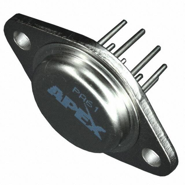
| 产品图片 |
|
| 产品型号 | PA61 |
| rohs | 无铅 / 符合限制有害物质指令(RoHS)规范要求 |
| 产品系列 | Apex Precision Power® |
| 产品培训模块 | http://www.digikey.cn/PTM/IndividualPTM.page?site=cn&lang=zhs&ptm=30464 |
| 产品目录页面 | |
| 供应商器件封装 | TO-3-8 |
| 其它名称 | 598-1317 |
| 包装 | 管件 |
| 压摆率 | 2.8 V/µs |
| 增益带宽积 | 1MHz |
| 安装类型 | 通孔 |
| 封装/外壳 | TO-3-8 |
| 工作温度 | -25°C ~ 85°C |
| 放大器类型 | 功率 |
| 标准包装 | 1 |
| 电压-电源,单/双 (±) | 20 V ~ 90 V, ±10 V ~ 45 V |
| 电压-输入失调 | 2mV |
| 电流-电源 | 3mA |
| 电流-输入偏置 | 12nA |
| 电流-输出/通道 | 10A |
| 电路数 | 1 |
| 输出类型 | - |


- 商务部:美国ITC正式对集成电路等产品启动337调查
- 曝三星4nm工艺存在良率问题 高通将骁龙8 Gen1或转产台积电
- 太阳诱电将投资9.5亿元在常州建新厂生产MLCC 预计2023年完工
- 英特尔发布欧洲新工厂建设计划 深化IDM 2.0 战略
- 台积电先进制程称霸业界 有大客户加持明年业绩稳了
- 达到5530亿美元!SIA预计今年全球半导体销售额将创下新高
- 英特尔拟将自动驾驶子公司Mobileye上市 估值或超500亿美元
- 三星加码芯片和SET,合并消费电子和移动部门,撤换高东真等 CEO
- 三星电子宣布重大人事变动 还合并消费电子和移动部门
- 海关总署:前11个月进口集成电路产品价值2.52万亿元 增长14.8%


PDF Datasheet 数据手册内容提取
PA61 • PA61A RoHS Power Operational Amplifiers COMPLIANT FEATURES • Wide Supply Range — ±10 to ±45V • High Output Current — ±10A Peak • Low Cost — Class “C” Output Stage • Low Quiescent Current — 3mA APPLICATIONS • Programmable Power Supply • Motor/Syncro Driver • Valve And Actuator Control • DC or AC Power Regulator • Fixed Frequency Power Oscillator DESCRIPTION The PA61 and PA61A are high output current operational amplifiers designed to drive resistive, inductive and capacitive loads. Their complementary emitter follower output stage is the simple class C type and opti‐ mized for low frequency applications where crossover distortion is not critical. These amplifiers are not rec‐ ommended for audio, transducer or deflection coil drive circuits above 1 kHz or when distortion is critical. The safe operating area (SOA) is fully specified and can be observed for all operating conditions by selection of user programmable current limiting resistors. Both amplifiers are internally compensated for all gain set‐ tings. For continuous operation under load, mounting on a heatsink of proper rating is recommended. This hybrid circuit utilizes thick film conductors, ceramic capacitors, and semiconductor chips to maxi‐ mize reliability, minimize size, and give top performance. Ultrasonically bonded aluminum wires provide reli‐ able interconnections at all operating temperatures. The 8‐pin TO‐3 package is electrically isolated and hermetically sealed. The use of compressible thermal washers and/or improper mounting torque voids the product warranty. Please see Application Note 1, “General Operating Considerations”. Figure 1: Equivalent Schematic 3 Q1A Q1B 2 Q3 4 A1 1 5 Q4 8 C1 Q6B Q6A 6 © Apex Microtechnology Inc. Dec 2015 www.apexanalog.com All rights reserved PA61U Rev P
PA61 • PA61A TYPICAL CONNECTION Figure 2: Typical Connection 2 PA61U Rev P
PA61 • PA61A PINOUT AND DESCRIPTION TABLE Figure 3: External Connections Pin Number Name Description 1 OUT The output. Connect this pin to load and to the feedback resistors. Connect to the sourcing current limit resistor. Output current flows into/out of this 2 +CL pin through RCL+. The output pin and the load are connected to the other side of R . CL+ 3 ‐Vs The positive supply rail. 4 +IN The non‐inverting input. 5 ‐IN The inverting input. 6 ‐Vs The negative supply rail. 7 NC No connection. Connect to the sinking current limit resistor. Output current flows into/out of this 8 ‐CL pin through R . The output pin and the load are connected to the other side of R CL‐ CL‐ . PA61U Rev P 3
PA61 • PA61A SPECIFICATIONS The power supply voltage for all specifications is the TYP rating unless noted as a test condition. ABSOLUTE MAXIMUM RATINGS Parameter Symbol Min Max Units Supply Voltage, total +V to ‐V 90 V s s Output Current, within SOA I 10 A O Power Dissipation, internal P 97 W D Input Voltage, differential V ±37 V IN (Diff) Input Voltage, common mode V ±V V cm S Temperature, pin solder, 10s max. 350 °C Temperature, junction 1 TJ 200 °C Temperature Range, storage ‐65 +150 °C Operating Temperature Range, case T ‐55 +125 °C C 1. Long term operation at the maximum junction temperature will result in reduced product life. Derate internal power dis‐ sipation to achieve high MTTF. The internal substrate contains beryllia (BeO). Do not break the seal. If accidentally broken, do CAUTION not crush, machine, or subject to temperatures in excess of 850°C to avoid generating toxic fumes. 4 PA61U Rev P
PA61 • PA61A INPUT PA61 PA61A Test Parameter Units Conditions Min Typ Max Min Typ Max Offset Voltage, initial T = 25°C ±2 ±6 ±1 ±4 mV C Specified temp Offset Voltage vs. Temperature ±10 ±65 * ±40 µV/°C range Offset Voltage vs. Supply T = 25°C ±30 ±200 * * µV/V C Offset Voltage vs. Power T = 25°C ±20 * µV/W C Bias Current, initial T = 25°C 12 30 10 20 nA C Specified temp Bias Current vs. Temperature ±50 ±500 * * pA/°C range Bias Current vs. Supply T = 25°C ±10 * pA/V C Offset Current, initial T = 25°C ±12 ±30 ±5 ±10 nA C Specified temp Offset Current vs. Temperature ±50 * pA/°C range Input Impedance, DC T = 25°C 200 * MΩ C Input Capacitance T = 25°C 3 * pF C Specified temp Common Mode Voltage Range 1 range ±VS – 5 ±VS – 3 * * V Specified temp Common Mode Rejection, DC 1 74 100 * * dB range 1. +V and –V denote the positive and negative supply rail respectively. Total V is measured from +V to –V . S S S S S GAIN PA61 PA61A Test Parameter Units Conditions Min Typ Max Min Typ Max Full temp range, Open Loop @ 10 Hz 96 108 * * dB full load T = 25°C, full Gain Bandwidth Product @ 1 MHz C 1 * MHz load T = 25°C, I = C O Power Bandwidth 10 16 * * kHz 8A, V = 40V O PP Phase Margin Full temp range 45 * ° PA61U Rev P 5
PA61 • PA61A OUTPUT PA61 PA61A Test Parameter Units Conditions Min Typ Max Min Typ Max Voltage Swing 1 TC=25°C, IO=10A ±VS–7 ±VS–5 ±VS–6 * V Full temp range, Voltage Swing 1 I = 4A ±VS–6 ±VS–4 * * V O Full temp range, Voltage Swing 1 I = 68mA ±VS–5 * V O Current T = 25°C ±10 * A C Settling Time to 0.1% T =25°C, 2V step 2 * µs C Slew Rate T =25°C, R =6 Ω 1.0 2.8 * * V/µs C L Capacitive Load, unit gain Full temp range 1.5 * nF Capacitive Load, gain > 4 Full temp range SOA * 1. +V and –V denote the positive and negative supply rail respectively. Total V is measured from +V to –V . S S S S S POWER SUPPLY PA61 PA61A Test Parameter Units Conditions Min Typ Max Min Typ Max Voltage Full temp range ±10 ±32 ±45 * * * V Current, quiescent T = 25°C 3 10 * * mA C THERMAL PA61 PA61A Test Parameter Units Conditions Min Typ Max Min Typ Max Resistance, AC, junction to case 1 F > 60 Hz 1.0 1.2 * * °C/W Resistance, DC, junction to case F < 60 Hz 1.5 1.8 * * °C/W Resistance, junction to air 30 * °C/W Meets full range Temperature Range, case ‐25 25 +85 * * * °C specs 1. Rating applies if the output current alternates between both output transistors at a rate faster than 60 Hz. Note: * The specification of PA61A is identical to the specification for PA61 in applicable column to the left. 6 PA61U Rev P
PA61 • PA61A TYPICAL PERFORMANCE GRAPHS Figure 4: Power Derating Figure 5: Output Voltage Swing 100 5.5 ) (cid:116) T = T V) 5.0 (cid:374)(cid:853)(cid:3)(cid:87)(cid:3)(cid:894) 80 C ply ( (cid:381) p (cid:415) u 4.5 (cid:258) S (cid:381)(cid:449)(cid:286)(cid:396)(cid:3)(cid:24)(cid:349)(cid:400)(cid:400)(cid:349)(cid:393) 6400 Drop From 43..05 T C = T – 2= 5 °2 C5 t o 8 5 ° C (cid:87) e C (cid:258)(cid:367)(cid:3) ag (cid:410)(cid:286)(cid:396)(cid:374) 20 Volt 3.0 (cid:374) (cid:47) 0 2.5 0 25 50 75 100 125 150 0 2 4 6 8 10 Temperature, T (°C) Output Current, I (A) C O Figure 6: Small Signal Response Figure 7: Phase Response 120 0 100 -30 ) B (d 80 -60 OL A ) ain, 60 (°(cid:588)(cid:3) -90 G e, p 40 as -120 o h o P L n 20 -150 e p O 0 -180 -20 -210 1 10 100 1k 10k .1M 1M 10M 1 10 100 1k 10k .1M 1M 10M Frequency, F (Hz) Frequency, F (Hz) PA61U Rev P 7
PA61 • PA61A Figure 8: Current Limit Figure 9: Power Response 7 80 V = ±40V S 6 58 ) t, I(A) LIM 54 RCL(cid:3)(cid:1089)(cid:3)(cid:1004)(cid:856)(cid:1005)(cid:1006)(cid:3)(cid:591)(cid:3)(cid:3)(cid:3)(cid:3) e, V(VO P-P 4310 RL(cid:3)(cid:1089)(cid:3)(cid:1012)(cid:3)(cid:591) mi ag nt Li 3 Volt 21 urre 2 RCL(cid:3)(cid:1089)(cid:3)(cid:1004)(cid:856)(cid:1007)(cid:3)(cid:591) tput 15 C u O R(cid:3)(cid:1089)(cid:3)(cid:1007)(cid:3)(cid:591) L 1 11 0 8 -25 0 25 50 75 100 125 10k 20k 30k 50k 70k .1M Case Temperature, T (°C) Frequency, F (Hz) C Figure 10: Pulse Response Figure 11: Common Mode Rejection 8 120 A = +1 R(cid:3)(cid:1089)(cid:3)(cid:1009)(cid:3)(cid:591) (cid:17)(cid:895) 6 V L (cid:282) (cid:90)(cid:3)(cid:894) 100 (cid:68) ) 4 V (cid:18) (O (cid:374)(cid:853)(cid:3) 80 V 2 (cid:381) e (cid:415) g (cid:272) a (cid:286) olt 0 (cid:90)(cid:286)(cid:361) 60 V (cid:286)(cid:3) t -2 (cid:282) pu (cid:68)(cid:381) 40 t Ou -4 (cid:374)(cid:3) (cid:381) (cid:373) 20 -6 (cid:373) (cid:381) (cid:18) -8 0 0 2 4 6 8 10 12 14 1 10 100 1k 10k .1M 1M Time, t (μs) Frequency, F (Hz) 8 PA61U Rev P
PA61 • PA61A Figure 12: Bias Current Figure 13: Harmonic Distortion 2.5 10 V = ±36 S ) 2.2 R(cid:3)(cid:1089)(cid:3)(cid:1008)(cid:3)(cid:591) X 3 L (B A = 10 Current, I 11..69 %)(cid:374)(cid:3)(cid:894) 1 V P O= 0.1 W s (cid:415)(cid:381) 0.3 ed Bia 1.3 (cid:24)(cid:349)(cid:400)(cid:410)(cid:381)(cid:396) 0.1 P O= 5 W z W ali 1.0 50 m = r P O No .7 0.03 .4 0.01 –50 –25 0 25 50 75 100 125 30 100 300 1k 3k 10k 30k Case Temperature, T (°C) Frequency, F (Hz) C Figure 14: Quiescent Current Figure 15: Input Noise 1.6 100 ) X t, I (Q 1.4 Hz) (cid:1103) 70 n / e V r n 50 r 1.2 ( u V nt C T = 125°C ge, 40 ce 1.0 C ta 30 d Quies 0.8 TC = 25°C T = – 5 5°C oise Vol 20 e C N z ali ut m 0.6 p r n o I N 0.4 10 20 30 40 50 60 70 80 90 10 100 1k 10k .1M Total Supply Voltage, V (V) Frequency, F (Hz) S PA61U Rev P 9
PA61 • PA61A SAFE OPERATING AREA (SOA) The output stage of most power amplifiers has 3 distinct limitations: 1. The current handling capability of the transistor geometry and the wire bonds. 2. The second breakdown effect which occurs whenever the simultaneous collector current and collector‐ emitter voltage exceeds specified limits. 3. The junction temperature of the output transistors. The SOA curves combine the effect of all limits for this Power Op Amp. For a given application, the direc‐ tion and magnitude of the output current should be calculated or measured and checked against the SOA curves. This is simple for resistive loads but more complex for reactive and EMF generating loads. The follow‐ ing guidelines may save extensive analytical efforts. 1. Under transient conditions, capacitive and dynamic* inductive loads up to the following maximum are safe: Capacitive Load Inductive Load ±V S I = 5A I = 10A I = 5A I = 10A LIM LIM LIM LIM 45V 200 F 150 F 8 mH 2.8 mH 40V 400 F 200 F 11 mH 4.3 mH 35V 800 F 400 F 20 mH 5.0 mH 30V 160 F 800 F 35 mH 6.2 mH 25V 5mF 2.5mF 50 mH 15 mH 20V 10mF 5mF 400 mH 20 mH 15V 20mF 10mF ** 100 mH * If the inductive load is driven near steady state conditions, allowing the output voltage to drop more than 8V below the supply rail with I = 10A or 15V below the supply rail with I = 5A while the amplifier is LIM LIM current limiting, the inductor should be capacitively coupled or the current limit must be lowered to meet SOA criteria. ** Second breakdown effect imposes no limitation but thermal limitations must still be observed. 2. The amplifier can handle any EMF generating or reactive load and short circuits to the supply rail or shorts to common if the current limits are set as follows at T = 85°C. C Short to ±V ±V S Short to Common S C, L, or EMF Load 45V 0.1A 1.3A 40V 0.2A 1.5A 35V 0.3A 1.6A 30V 0.5A 2.0A 25V 1.2A 2.4A 20V 1.5A 3.0A 15V 2.0A 4.0A * These simplified limits may be exceeded with further analysis using the operating conditions for a specific application. 10 PA61U Rev P
PA61 • PA61A 3. The output stage is protected against transient flyback. However, for protection against sustained, high energy flyback, external fast‐recovery diodes should be used. Figure 16: SOA 10 8.0 ) 6.0 t +V or -V(ASS 432...000 TC =TTC 1C =2 = 58 2°5C5°°CC t = 5t = =1 m0.5sms 1.5 m m (cid:94) s o 1.0 (cid:410)(cid:286) r (cid:258) F 0.8 (cid:282) t (cid:455)(cid:3) n 0.6 (cid:94)(cid:410) e (cid:258) r (cid:410) r 0.4 (cid:286) u C 0.3 t u p 0.2 n I 0.1 10 15 20 25 30 40 50 6070 8090 (cid:94)(cid:437)(cid:393)(cid:393)(cid:367)(cid:455)(cid:3)(cid:410)(cid:381)(cid:3)(cid:75)(cid:437)(cid:410)(cid:393)(cid:437)(cid:410)(cid:3)(cid:24)(cid:349)(cid:299)(cid:286)(cid:396)(cid:286)(cid:374)(cid:415)(cid:258)(cid:367)(cid:853)(cid:3)V -V (V) S O PA61U Rev P 11
PA61 • PA61A GENERAL Please read Application Note 1 “General Operating Considerations” which covers stability, supplies, heat sinking, mounting, current limit, SOA interpretation, and specification interpretation. Visit www.apexana‐ log.com for Apex Microtechnology’s complete Application Notes library, Technical Seminar Workbook, and Evaluation Kits. TYPICAL APPLICATION Due to its high current drive capability, PA61 applications often utilize remote sensing to compensate IR drops in the wiring. The importance of remote sensing increases as accuracy requirements, output currents, and distance between amplifier and load go up. The circuit above shows wire resistance from the PA61 to the load and back to the local ground via the power return line. Without remote sensing, a 7.5A load current across only 0.05 ohm in each line would produce a 0.75V error at the load. With the addition of the second ratio matched R /R pair and two low current sense wires, IR drops in F IN the power return line become common mode voltages for which the op amp has a very high rejection ratio. Voltage drops in the output and power return wires are inside the feedback loop. Therefore, as long as the Power Op Amp has the voltage drive capability to overcome the IR losses, accuracy remains the same. Appli‐ cation Note 7 presents a general discussion of PPS circuits. Figure 17: Typical Application (Programmable Power Supply With Remote Sensing) 12 PA61U Rev P
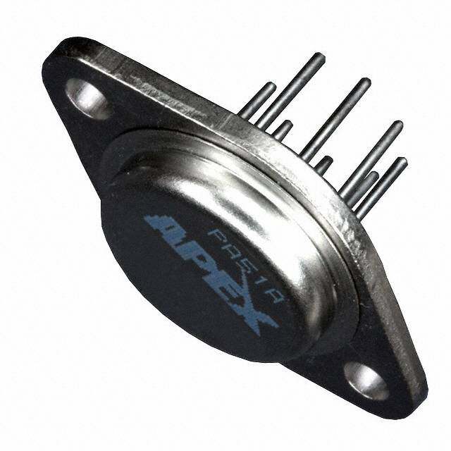
PA61 • PA61A PACKAGE OPTIONS Part Number Apex Package Style Description PA61 CE 8‐pin TO‐3 PA61A CE 8‐pin TO‐3 PACKAGE STYLE CE PA61U Rev P 13
PA61 • PA61A NEED TECHNICAL HELP? CONTACT APEX SUPPORT! For all Apex Microtechnology product questions and inquiries, call toll free 800-546-2739 in North America. For inquiries via email, please contact apex.support@apexanalog.com. International customers can also request support by contacting their local Apex Microtechnology Sales Representative. To find the one nearest to you, go to www.apexanalog.com IMPORTANT NOTICE Apex Microtechnology, Inc. has made every effort to insure the accuracy of the content contained in this document. However, the information is subject to change without notice and is provided "AS IS" without warranty of any kind (expressed or implied). Apex Microtechnology reserves the right to make changes without further notice to any specifications or products mentioned herein to improve reliability. This document is the property of Apex Microtechnology and by furnishing this information, Apex Microtechnology grants no license, expressed or implied under any patents, mask work rights, copyrights, trademarks, trade secrets or other intellectual property rights. Apex Microtechnology owns the copyrights associated with the information contained herein and gives consent for copies to be made of the information only for use within your organization with respect to Apex Microtechnology integrated circuits or other products of Apex Microtechnology. This consent does not extend to other copying such as copying for general distribution, advertising or promotional purposes, or for creating any work for resale. APEX MICROTECHNOLOGY PRODUCTS ARE NOT DESIGNED, AUTHORIZED OR WARRANTED TO BE SUITABLE FOR USE IN PRODUCTS USED FOR LIFE SUPPORT, AUTOMOTIVE SAFETY, SECURITY DEVICES, OR OTHER CRITICAL APPLICATIONS. PRODUCTS IN SUCH APPLICATIONS ARE UNDERSTOOD TO BE FULLY AT THE CUSTOMER OR THE CUSTOMER’S RISK. Apex Microtechnology, Apex and Apex Precision Power are trademarks of Apex Microtechnology, Inc. All other corporate names noted herein may be trademarks of their respective holders. 14 PA61U Rev P