ICGOO在线商城 > 集成电路(IC) > 线性 - 放大器 - 仪表,运算放大器,缓冲器放大器 > TS507ILT
 Datasheet下载
- 型号: TS507ILT
- 制造商: STMicroelectronics
- 库位|库存: xxxx|xxxx
- 要求:
| 数量阶梯 | 香港交货 | 国内含税 |
| +xxxx | $xxxx | ¥xxxx |
查看当月历史价格
查看今年历史价格
TS507ILT产品简介:
ICGOO电子元器件商城为您提供TS507ILT由STMicroelectronics设计生产,在icgoo商城现货销售,并且可以通过原厂、代理商等渠道进行代购。 TS507ILT价格参考。STMicroelectronicsTS507ILT封装/规格:线性 - 放大器 - 仪表,运算放大器,缓冲器放大器, 通用 放大器 1 电路 满摆幅 SOT-23-5。您可以下载TS507ILT参考资料、Datasheet数据手册功能说明书,资料中有TS507ILT 详细功能的应用电路图电压和使用方法及教程。
TS507ILT 是 STMicroelectronics 生产的一款高性能仪表放大器,属于线性 - 放大器 - 仪表、运算放大器、缓冲器放大器类别。它具有低功耗、高精度和宽电源电压范围的特点,适合多种应用场景。以下是其主要应用场景:

1. 工业测量:TS507ILT 可用于工业自动化中的传感器信号调理,例如压力传感器、温度传感器或应变片等微弱信号的放大与处理。其高共模抑制比 (CMRR) 和低偏移特性使其非常适合在嘈杂的工业环境中使用。

2. 医疗设备:在医疗领域,该器件可用于心电图 (ECG)、脑电图 (EEG) 或肌电图 (EMG) 等生物电信号的采集与放大。它的低噪声性能能够确保对微弱生理信号的精确捕捉。

3. 音频处理:TS507ILT 的低失真特性也适用于高品质音频信号的放大,例如麦克风前置放大器或音频混音器中,以提高信噪比并减少失真。

4. 汽车电子:在汽车应用中,这款放大器可以用于电池管理系统的电压监测、车载传感器信号处理(如氧传感器或胎压传感器)以及动力总成控制单元中的信号调理。

5. 消费电子:对于需要精密信号放大的消费电子产品,如智能家居设备、可穿戴设备或便携式仪器,TS507ILT 提供了小型化封装和低功耗优势,延长电池寿命同时保持高性能。

6. 数据采集系统 (DAQ):作为多通道数据采集系统的一部分,TS507ILT 能够准确地放大来自不同类型的传感器输入信号,并将其转换为适合后续 ADC 处理的形式。

总之,TS507ILT 凭借其优异的技术参数,在任何需要高精度、低噪声和稳定性的信号放大场合都能发挥重要作用。
| 参数 | 数值 |
| -3db带宽 | - |
| 产品目录 | 集成电路 (IC)半导体 |
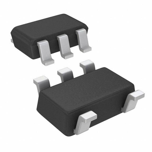
| 描述 | IC OPAMP GP 1.9MHZ RRO SOT23-5精密放大器 Hi precision op amp |
| 产品分类 | Linear - Amplifiers - Instrumentation, OP Amps, Buffer Amps集成电路 - IC |
| 品牌 | STMicroelectronics |
| 产品手册 | |
| 产品图片 |
|
| rohs | 符合RoHS无铅 / 符合限制有害物质指令(RoHS)规范要求 |
| 产品系列 | 放大器 IC,精密放大器,STMicroelectronics TS507ILT- |
| 数据手册 | |
| 产品型号 | TS507ILT |
| 产品目录页面 | |
| 产品种类 | 精密放大器 |
| 供应商器件封装 | SOT-23-5 |
| 其它名称 | 497-8118-2 |
| 其它有关文件 | http://www.st.com/web/catalog/sense_power/FM123/SC61/SS1613/LN1589/PF89213?referrer=70071840http://www.st.com/web/catalog/sense_power/FM123/SC61/SS1613/LN1591/PF89213?referrer=70071840 |
| 包装 | 带卷 (TR) |
| 压摆率 | 0.6 V/µs |
| 参考设计库 | http://www.digikey.com/rdl/4294959886/4294959870/766 |
| 商标 | STMicroelectronics |
| 增益带宽生成 | 1.9 MHz |
| 增益带宽积 | 1.9MHz |
| 安装类型 | 表面贴装 |
| 安装风格 | SMD/SMT |
| 封装 | Reel |
| 封装/外壳 | SC-74A,SOT-753 |
| 封装/箱体 | SOT23-5 |
| 工作温度 | -40°C ~ 125°C |
| 工作电源电压 | 2.7 V to 5.5 V |
| 工厂包装数量 | 3000 |
| 放大器类型 | 通用 |
| 最大工作温度 | + 125 C |
| 最小工作温度 | - 40 C |
| 标准包装 | 3,000 |
| 电压-电源,单/双 (±) | 2.7 V ~ 5.5 V |
| 电压-输入失调 | 25µV |
| 电流-电源 | 850µA |
| 电流-输入偏置 | 8nA |
| 电流-输出/通道 | 128mA |
| 电源电压-最大 | 5.5 V |
| 电源电压-最小 | 2.7 V |
| 电源电流 | 1.15 mA |
| 电源类型 | Single |
| 电路数 | 1 |
| 系列 | TS507 |
| 输入电压范围—最大 | 0 V to 5.5 V |
| 输入补偿电压 | 25 uV |
| 输出类型 | 满摆幅 |
| 通道数量 | 1 Channel |


- 商务部:美国ITC正式对集成电路等产品启动337调查
- 曝三星4nm工艺存在良率问题 高通将骁龙8 Gen1或转产台积电
- 太阳诱电将投资9.5亿元在常州建新厂生产MLCC 预计2023年完工
- 英特尔发布欧洲新工厂建设计划 深化IDM 2.0 战略
- 台积电先进制程称霸业界 有大客户加持明年业绩稳了
- 达到5530亿美元!SIA预计今年全球半导体销售额将创下新高
- 英特尔拟将自动驾驶子公司Mobileye上市 估值或超500亿美元
- 三星加码芯片和SET,合并消费电子和移动部门,撤换高东真等 CEO
- 三星电子宣布重大人事变动 还合并消费电子和移动部门
- 海关总署:前11个月进口集成电路产品价值2.52万亿元 增长14.8%


PDF Datasheet 数据手册内容提取
TS507 High precision rail-to-rail operational amplifier Datasheet - production data Applications Pin connections (top view) • Battery-powered applications • Portable devices OOuuttppuutt 11 55 VVCCCC • Signal conditioning • Medical instrumentation VVDDDD 22 NNoonn IInnvveerrttiinngg IInnppuutt 33 44 IInnvveerrttiinngg IInnppuutt Description SOT23-5 The TS507 is a high performance rail-to-rail input/output amplifier with very low offset voltage. This amplifier uses a new trimming technique that NN..CC.. 11 88 NN..CC.. yields ultra low offset voltages without any need for external zeroing. IInnvveerrttiinngg IInnppuutt 22 __ 77 VVCCCC NNoonn IInnvveerrttiinngg IInnppuutt 33 ++ 66 OOuuttppuutt The circuit offers very stable electrical characteristics over the entire supply voltage VVDDDD 44 55 NN..CC.. range, and is particularly intended for automotive and industrial applications. SO-8 The TS507 is housed in the space-saving 5-pin SOT23 package, making it well suited for battery- powered systems. This micropackage simplifies Features the PC board design because of its ability to be placed in small spaces (external dimensions are • Ultra low offset voltage: 25 µV typ, 100 µV max 2.8 mm x 2.9 mm). • Rail-to-rail input/output voltage swing • Operates from 2.7 V to 5.5 V • High speed: 1.9 MHz • 45° phase margin with 100 pF • Low consumption: 0.8 mA at 2.7 V • Very large signal voltage gain: 131 dB • High-power supply rejection ratio: 105 dB • Very high ESD protection 5kV (HBM) • Latchup immunity • Available in SOT23-5 micropackage • Automotive qualification March 2013 DocID10958 Rev 6 1/20 This is information on a product in full production. www.st.com 20
Contents TS507 Contents 1 Absolute maximum ratings and operating conditions . . . . . . . . . . . . . 3 2 Electrical characteristics . . . . . . . . . . . . . . . . . . . . . . . . . . . . . . . . . . . . . 4 3 Application note . . . . . . . . . . . . . . . . . . . . . . . . . . . . . . . . . . . . . . . . . . . 15 3.1 Out-of-the-loop compensation technique . . . . . . . . . . . . . . . . . . . . . . . . . 15 3.2 In-the-loop-compensation technique . . . . . . . . . . . . . . . . . . . . . . . . . . . . 16 4 Package information . . . . . . . . . . . . . . . . . . . . . . . . . . . . . . . . . . . . . . . . 17 4.1 SOT23-5 package information . . . . . . . . . . . . . . . . . . . . . . . . . . . . . . . . . 17 4.2 SO-8 package . . . . . . . . . . . . . . . . . . . . . . . . . . . . . . . . . . . . . . . . . . . . . 18 5 Ordering information . . . . . . . . . . . . . . . . . . . . . . . . . . . . . . . . . . . . . . . 19 6 Revision history . . . . . . . . . . . . . . . . . . . . . . . . . . . . . . . . . . . . . . . . . . . 19 2/20 DocID10958 Rev 6
TS507 Absolute maximum ratings and operating conditions 1 Absolute maximum ratings and operating conditions Table 1. Absolute maximum ratings (AMR) Symbol Parameter Value Unit V Supply voltage(1) 6 CC V Differential input voltage(2) ±2.5 V id V Input voltage(3) V -0.3 to V +0.3 in DD CC T Storage temperature -65 to +150 °C stg Thermal resistance junction to ambient(4)(5) Rthja SOT23-5 250 SO-8 125 °C/W Thermal resistance junction to case Rthjc SOT23-5 81 SO-8 40 T Maximum junction temperature 150 °C j HBM: human body model(6) 5 kV ESD MM: machine model(7) 300 V CDM: charged device model(8) 2 kV Latchup immunity class A 1. Value with respect to V pin. DD 2. Differential voltages are the non-inverting input terminal with respect to the inverting input terminal. 3. V -V and V must not exceed 6 V. CC in in 4. Short-circuits can cause excessive heating and destructive dissipation. 5. R are typical values. thja/c 6. Human body model: A 100 pF capacitor is charged to the specified voltage, then discharged through a 1.5 kΩ resistor between two pins of the device. This is done for all couples of connected pin combinations while the other pins are floating. 7. Machine model: A 200 pF capacitor is charged to the specified voltage, then discharged directly between two pins of the device with no external series resistor (internal resistor < 5 Ω). This is done for all couples of connected pin combinations while the other pins are floating. 8. Charged device model: all pins and the package are charged together to the specified voltage and then discharged directly to the ground through only one pin. This is done for all pins. Table 2. Operating conditions Symbol Parameter Value Unit V Supply voltage(1) 2.7 to 5.5 CC V Common mode input voltage range V to V V icm DD CC V Differential input voltage(2) ±2.5 id Operating free air temperature range Toper TS507C 0 to +85 °C TS507I -40 to +125 1. Value with respect to V pin. DD 2. Differential voltages are the non-inverting input terminal with respect to the inverting input terminal. DocID10958 Rev 6 3/20
Electrical characteristics TS507 2 Electrical characteristics Table 3 . Electrical characteristics at V = +5 V, V = 0 V, V = V /2, T = 25 °C, CC DD icm CC amb R connected to V /2 (unless otherwise specified)(1) L CC Symbol Parameter Conditions Min. Typ. Max. Unit DC performance V = 0 to 3.8 V, T=25 °C 25 100 icm TS507C full temperature range 250 TS507I full temperature range 400 V Input offset voltage(2) µV io V = 0 V to 5 V, T=25 °C 450 icm TS507C full temperature range 550 TS507I full temperature range 750 ΔV /Δt V drift vs. temperature T < T < T 1 µV/°C io io min op max T = 25 °C 8 70 I Input bias current TS507C full temperature range 75 ib TS507I full temperature range 110 nA T = 25 °C 2 25 I Input offset current TS507C full temperature range 35 io TS507I full temperature range 50 V from 0 V to 3.8 V, T=25 °C 94 115 icm Common mode rejection ratio TS507C full temperature range 94 CMRR 20 log (ΔV /ΔV ) TS507I full temperature range 91 icm io V from 0 V to 5 V 96 icm V from 2.7 V to 5.5 V, CC dB Power supply rejection ratio Vicm=Vcc/2, T=25 °C 91 105 PSRR 20 log (ΔVCC/ΔVio) TS507C full temperature range 90 TS507I full temperature range 89 R = 10 kΩ, V = 0.5 V to 4.5 V 99 131 A Large signal voltage gain L out vd Full temperature range 98 R = 600Ω, T=25°C 67 95 L TS507C full temperature range 110 V -V High level output voltage drop TS507I full temperature range 120 CC OH R = 10 kΩ, T=25 °C 4 15 L Full temperature range 15 mV R = 600 Ω, T=25 °C 64 90 L TS507C full temperature range 110 V Low level output voltage TS507I full temperature range 125 OL R = 10 kΩ, T=25 °C 4 15 L Full temperature range 15 4/20 DocID10958 Rev 6
TS507 Electrical characteristics Table 3. Electrical characteristics at V = +5 V, V = 0 V, V = V /2, T = 25 °C, CC DD icm CC amb R connected to V /2 (unless otherwise specified)(1) (continued) L CC Symbol Parameter Conditions Min. Typ. Max. Unit V = V V =-1 V, T=25 °C 74 104 out CC, id I TS507C full temperature range 60 sink TS507I full temperature range 53 I out V = V , V =1 V, T=25 °C 90 128 out DD id I TS507C full temperature range 77 mA source TS507I full temperature range 70 No load, V =V /2, out CC I Supply current (per operator)(2) V =0 to 5 V, T=25 °C 0.85 1.15 CC icm Full temperature range 1.25 Dynamic performance R = 2 kΩ, C = 100 pF, GBP Gain bandwidth product L L 1.9 MHz f = 100 kHz φ Phase margin 45 Degrees m R = 2 kΩ, C =100 pF L L G Gain margin 10 dB m R = 2 kΩ, C =100 pF, SR Slew rate VL = 1.25 V Lto 3.75 V, 0.6 V/µs out 10% to 90% e Equivalent input noise voltage f = 1 kHz 12 nV/√ Hz N i Equivalent input noise current f = 10 kHz 1.2 pA/√ Hz N f=1 kHz, G=1, R =2 kΩ, THD+e THD + noise L 0.0003 % N V =2 V, V =3.5 V icm out pp 1. All parameter limits at temperatures different from 25 ° C are guaranteed by correlation. 2. Measurements made at 4 V values: V =0 V, V =3.8 V, V =4.2 V, V =5 V. icm icm icm icm icm DocID10958 Rev 6 5/20
Electrical characteristics TS507 Table 4 . Electrical characteristics at V = +3.3 V, V = 0 V, V = V /2, T = 25 °C, CC DD icm CC amb R connected to V /2 (unless otherwise specified)(1) L CC Symbol Parameter Conditions Min. Typ. Max. Unit DC performance V = 0 to 2.1 V, T=25 °C 25 100 icm TS507C full temperature range 250 TS507I full temperature range 400 V Input offset voltage(2) µV io V = 0 V to 3.3 V, T=25 °C 450 icm TS507C full temperature range 550 TS507I full temperature range 750 ΔV V drift vs. temperature T < T < T 1 µV/°C io io min op max T = 25 °C 6 70 I Input bias current TS507C full temperature range 75 ib TS507I full temperature range 145 nA T = 25 °C 2 25 I Input offset current TS507C full temperature range 40 io TS507I full temperature range 45 Common mode rejection ratio CMRR V from 0 V to 2.1 V 115 20 log (ΔV /ΔV ) icm icm io dB A Large signal voltage gain R = 10 kΩ, V = 0.5 V to 2.8 V 127 vd L out R = 600 Ω, T=25 °C 59 85 L TS507C full temperature range 100 V -V High level output voltage drop TS507I full temperature range 110 CC OH R = 10 kΩ, T=25 °C 4 15 L Full temperature range 15 mV R = 600 Ω, T=25 °C 57 80 L TS507C full temperature range 100 V Low level output voltage TS507I full temperature range 115 OL R = 10 kΩ, T=25 °C 4 15 L Full temperature range 15 V = V V =-1 V, T=25 °C 33 48 out CC, id I TS507C full temperature range 26 sink TS507I full temperature range 22 I out V = V , V =1 V, T=25 °C 37 56 out DD id I TS507C full temperature range 32 mA source TS507I full temperature range 29 No load, V =V /2, out CC I Supply current (per operator)(2) V =0 to 3.3 V, T=25 °C 0.81 1.1 CC icm Full temperature range 1.2 6/20 DocID10958 Rev 6
TS507 Electrical characteristics Table 4. Electrical characteristics at V = +3.3 V, V = 0 V, V = V /2, T = 25 °C, CC DD icm CC amb R connected to V /2 (unless otherwise specified)(1) (continued) L CC Symbol Parameter Conditions Min. Typ. Max. Unit Dynamic performance R = 2 kΩ, C = 100 pF, GBP Gain bandwidth product L L 1.9 MHz f = 100 kHz φ Phase margin 45 Degrees m R = 2 kΩ, C =100 pF L L G Gain margin 10 dB m R = 2 kΩ, C =100 pF, L L SR Slew rate Vout= 0.5 V to 2.8 V, 0.6 V/µs 10 % to 90 % e Equivalent input noise voltage f = 1 kHz 12 nV/√ Hz N f=1 KHz, G=1, R =2 kΩ, THD+e THD + noise L 0.0004 % N V =1.15 V, V =1.8 V icm out pp 1. All parameter limits at temperatures different from 25 ° C are guaranteed by correlation. 2. Measurements done at 4 V values: V =0 V, V =2.1 V, V =2.5 V, V =3.3 V. icm icm icm icm icm DocID10958 Rev 6 7/20
Electrical characteristics TS507 Table 5 . Electrical characteristics at V = +2.7 V V = 0 V, V = V /2, T = 25 °C, CC DD icm CC amb R connected to V /2 (unless otherwise specified)(1) L CC Symbol Parameter Conditions Min. Typ. Max. Unit DC performance V = 0 to 1.9 V, T=25 °C 25 100 icm TS507C full temperature range 250 TS507I full temperature range 400 V Input offset voltage(2) µV io V = 0 V to 2.7 V, T=25 °C 450 icm TS507C full temperature range 550 TS507I full temperature range 750 ΔV V drift vs. temperature T < T < T 1 µV/°C io io min op max T = 25 °C 8 70 I Input bias current TS507C full temperature range 75 ib TS507I full temperature range 160 nA T = 25 °C 2 25 I Input offset current TS507C full temperature range 45 io TS507I full temperature range 45 Common mode rejection ratio CMRR V from 0 V to 1.5 V 115 20 log (ΔV /ΔV ) icm icm io dB A Large signal voltage gain R = 10 kΩ, V = 0.5 V to 2.2 V 126 vd L out R = 600 Ω, T=25 °C 57 85 L TS507C full temperature range 100 V -V High level output voltage drop TS507I full temperature range 105 CC OH R = 10 kΩ, T=25 °C 4 15 L Full temperature range 15 mV R = 600 Ω, T=25 °C 57 80 L TS507C full temperature range 100 V Low level output voltage TS507I full temperature range 115 OL R = 10 kΩ, T=25 °C 4 15 L Full temperature range 15 V = V V =-1 V, T=25 °C 20 30 out CC, id I TS507C full temperature range 15 sink TS507I full temperature range 13 I out V = V , V =1 V, T=25 °C 22 35 out DD id I TS507C full temperature range 19 mA source TS507I full temperature range 17 No load, V =V /2, out CC I Supply current (per operator)(2) V =0 to 2.7 V, T=25 °C 0.79 1.1 CC icm Full temperature range 1.2 8/20 DocID10958 Rev 6
TS507 Electrical characteristics Table 5. Electrical characteristics at V = +2.7 V V = 0 V, V = V /2, T = 25 °C, CC DD icm CC amb R connected to V /2 (unless otherwise specified)(1) (continued) L CC Symbol Parameter Conditions Min. Typ. Max. Unit Dynamic performance R = 2 kΩ, C = 100 pF, GBP Gain bandwidth product L L 1.9 MHz f = 100 kHz φ Phase margin 45 Degrees m R = 2 kΩ, C =100 pF L L G Gain margin 11 dB m R = 2 kΩ, C =100 pF, L L SR Slew rate V = 0.5 V to 2.2 V, 0.6 V/µs out 10 % to 90 % e Equivalent input noise voltage f = 1 kHz 12 nV/√ Hz N f=1 KHz, G=1, R =2 kΩ, THD+e THD + noise L 0.0005 % N V =0.85 V, V =1.2 V icm out pp 1. All parameter limits at temperatures different from 25 ° C are guaranteed by correlation. 2. Measurements done at 4 V values: V =0 V, V =1.5 V, V =1.9 V, V =2.7 V. icm icm icm icm icm DocID10958 Rev 6 9/20
Electrical characteristics TS507 Figure 1. Input offset voltage distribution for Figure 2. Input offset voltage distribution vs. V ≤ V -1.2 V at T=25 °C temperature for V ≤ V -1.2 V icm CC icm CC 30 400 350 25 Vio distribution at T=25°C for 0V<=Vicm<=Vcc-1.2V 235000 0V<=Vicm<=Vcc-1.2V 200 150 20 100 % pulation 15 Vio (µV) -1-0550000 Po 10 -150 -200 -250 5 -300 -350 -400 0 -50-40-30-20-10 0 10 20 30 40 50 60 70 80 90100110120130 -120 -100 -80 -60 -40 -20 0 20 40 60 80 100 120 Input offset voltage (µV) Temperature (°C) Figure 3. Input offset voltage distribution vs. Figure 4. Input offset voltage distribution for temperature for V ≥ V -0.8 V V ≤ V -1.2 V at T=25 °C after HTB icm CC icm CC 700 45 600 Vio distribution at T=25°C for 0V<=Vicm<=Vcc-1.2V 500 Vcc-0.8V<=Vicm<=Vcc 40 after HTB (1000 hours at 125°C) 400 35 300 200 30 100 % µV) 0 on 25 Vio ( --210000 pulati 20 -300 Po 15 -400 -500 10 -600 5 -700 -50-40-30-20-10 0 10 20 30 40 50 60 70 80 90100110120130 0 -100 -80 -60 -40 -20 0 20 40 60 80 100 Temperature (°C) Input offset voltage (µV) Figure 5. Input offset voltage distribution for Figure 6. Input offset voltage vs. input common V ≤ V -1.2 V at T=25 °C after THB mode voltage at T=25 °C icm CC 4400 35 Vcc=3.3V Vcc=2.7V Vio distribution at T=25°C for 0V<=Vicm<=Vcc-1.2V 2200 30 after THB (1000 hours at 85°C, humidity 85%) V) 25 μe ( 00 % ag opulation 1250 Offset Volt ----44220000 Vcc=5.5V Vcc=5V P ut 10 p --6600 n I 5 --8800 0 --110000 -120 -100 -80 -60 -40 -20 0 20 40 60 80 100 120 --22..55 --22..00 --11..55 --11..00 --00..55 00..00 Input offset voltage (µV) Vicm-Vcc (V) 10/20 DocID10958 Rev 6
TS507 Electrical characteristics Figure 7. Supply current vs. input common Figure 8. Supply current vs. supply voltage mode voltage in closed loop configuration at V =V /2 icm CC at V =5 V CC 11..00 11..00 T=125°C 0.8 0.8 mA)0.7 T=125°C mA)0.7 nt ( T=-40°C T=25°C nt ( T=25°C urre00..55 urre00..55 T=-40°C C C y y pl0.3 pl0.3 up Vcc=5V up S Closed loop S 0.2 0.2 Vicm=Vcc/2 00..00 00..00 00 11 22 33 44 55 00 11 22 33 44 55 Input common mode voltage (V) Supply voltage (V) Figure 9. Supply current vs. input common Figure 10. Supply current vs. input common mode voltage in follower configuration mode voltage in follower configuration at V =2.7 V at V =5 V CC CC 11..00 11..00 T=125°C 0.8 0.8 T=25°C A)0.7 A)0.7 nt (m nt (m T=125°C T=25°C urre00..55 T=-40°C urre00..55 T=-40°C C C y y pl0.3 pl0.3 p Follower configuration p Su Vcc=2.7V Su Follower configuration Vcc=5V 0.2 0.2 00..00 00..00 00..00 00..55 11..00 11..55 22..00 22..55 00 11 22 33 44 55 Input Common Mode Voltage (V) Input Common Mode Voltage (V) Figure 11. Output current vs. supply voltage Figure 12. Output current vs. output voltage at V =V /2 at V =2.7 V icm CC CC 150 4400 125 SVoidu =rc 1eV T=-40°C 3305 T=-40°C 110000 T=25°C 25 Source 75 T=125°C 2200 Vid=1V mA) 50 mA) 15 T=25°C T=125°C nt ( 25 nt ( 105 e Vicm=Vcc/2 e urr 00 urr 00 Vcc=2.7V ut C -25 ut C -1-05 utp -50 utp -15 T=125°C T=25°C O -75 O --2200 --110000 T=125°C -25 Sink Sink -30 Vid=-1V -125 Vid = -1V T=25°C T=-40°C -35 T=-40°C -150 --4400 33..00 33..55 44..00 44..55 55..00 55..55 00..00 00..55 11..00 11..55 22..00 22..55 Supply voltage (V) Output Voltage (V) DocID10958 Rev 6 11/20
Electrical characteristics TS507 Figure 13. Output current vs. output voltage Figure 14. Positive and negative slew rate vs. at V =5 V supply voltage CC 150 11..00 111002005 T=25°C SVoidu=r1cVe e (V/µs) 00..88 Positive slew rate T=125°C 75 T=-40°C Rat 00..66 nt (mA) 2550 T=125°C ve Slew 0000....2244 T=-40°C T=25°C ut Curre -2500 Vcc=5V T=125°C d Negati --0000....2200 VSiRn :: cfraolmcu l0a.t5eVd tforo Vmc c1-00%.5 Vto 90% T=-40°C Outp --7550 ve an --00..44 T=25°C --110000 Sink ositi --00..66 -125 Vid=-1V P --00..88 Negative slew rate T=125°C T=-40°C T=25°C -150 --11..00 00..00 11..00 22..00 33..00 44..00 55..00 2.0 2.5 33..00 3.5 4.0 4.5 55..00 5.5 6.0 Output Voltage (V) Supply Voltage (V) Figure 15. Voltage gain and phase vs. frequency Figure 16. Voltage gain and phase vs. frequency at V =5 V and V =2.5 V at T=25 °C at V =5 V and V =2.5 V at T=-40 °C CC icm CC icm 50 180 50 180 4400 Phase 150 4400 150 120 120 30 30 90 90 2200 Cl=100pF 2200 60 60 n (dB) 1000 Gain Cl=230pF 030 se (°) n (dB) 1000 Phase 030 se (°) Gai -10 -30 Pha Gai -10 Gain -30 Pha --2200 Vcc=5V, Vicm=2.5V, G= -100 -60 --2200 -60 Rl=2kOhms, Vrl=Vcc/2 -90 -90 -30 Tamb=25°C -30 Vcc=5V, Vicm=2.5V, G= -100 -120 Rl=2kOhms, Cl=100pF, Vrl=Vcc/2 -120 --4400 -150 --4400 Tamb=-40°C -150 -50 -180 -50 -180 104 105 106 107 104 105 106 107 Frequency (Hz) Frequency (Hz) Figure 17. Voltage gain and phase vs. frequency Figure 18. Closed loop gain in voltage follower at V =5 V and V =2.5 V at T=125 °C configuration for different capacitive load CC icm at T=25 °C 50 180 2200 4400 115500 TS507 : V = 5 V 30 112200 10 Vciccm = 2,5 V 9900 T = 25 °C 2200 6600 00 RL = 10 kΩ Gain (dB) -110000 Gain Phase --033330000 Phase (°) Gain (dB) -10 GGaainin w witihtho uCt C=3L00 pF --2200 --6600 --2200 L Vcc=5V, Vicm=2.5V, G= -100 --9900 -30 Rl=2kOhms, Cl=100pF, Vrl=Vcc/2 --112200 -30 Gain with CL=550 pF --4400 Tamb=125°C --115500 -50 -180 --4400 104 105 106 107 10k 100k 1M 10M Frequency (Hz) Frequency (Hz) 12/20 DocID10958 Rev 6
TS507 Electrical characteristics Figure 19. Gain margin according to the output Figure 20. Phase margin according to the load, at V =5 V and T=25 °C output load, at V =5 V and T=25 °C CC CC 1E-6 1E-6 V = 5 V V = 5 V cc cc 1E-7 VTaicmmb == 22,55 °VC 1E-7 0 ° UNSTABLE VTaicmmb == 22,55 °VC d Capacitor (F) 11EE--98 UNSTABLE0 dB d Capacitor (F) 11EE--98 10 ° Loa 1E-10 10 dB Loa 1E-10 20 ° 30 ° 1E-11 30 dB 20 dB 1E-11 40 ° STABLE STABLE 50 ° 1E-12 1E-12 1 10 100 1k 10k 100k 1M 10M 1 10 100 1k 10k 100k 1M 10M Load Resistor (Ω) Load Resistor (Ω) Figure 21. Gain margin vs. output current, Figure 22. Phase margin vs. output current, at V =5 V and T=25 °C at V =5 V and T=25 °C CC CC 2200..00 70 17.5 Recommended area 6600 Recommended area 1155..00 100 pF 50 n Margin (dB) 1117002....5005 550 pF 300 pF se Margin (°) 344000 550 pF 100 pF 300 pF Gai 55..00 Pha 2200 V = 5 V V = 5 V 2.5 Vcc = 2,5 V 10 Vcc = 2,5 V 00..00 TRaicm m=b =2 2k5Ω °C 00 TRaicm m=b =2 2k5Ω °C L L -2.5 -10 --44 -3 --22 -1 00 1 22 3 44 --44 -3 --22 -1 00 1 22 3 44 Output Current (mA) Output Current (mA) Figure 23. Phase and gain margins vs Figure 24. Distortion + noise vs. output voltage capacitive load at = 25 °C 30 75 0.1000 V = 5 V cc 2200 VTicm == 22,55 °VC 50 Vcc=5V Ram =b 2 kΩ 10 L 25 0.0100 Gain (dB) -1000 Gain Margin -025 Phase (°) HD + N (%) f=1kHz VccV=c3c.=3V2.7V T 0.0010 Rl=2kOhms --2200 -50 Gain=1 Phase Margin BW=22kHz -30 -75 Vicm=(Vcc-1V)/2 --440010p 100p 1n 10n-100 0.0001 0.01 0.1 1 Load Capacitor (F) Output Voltage (Vpp) DocID10958 Rev 6 13/20
Electrical characteristics TS507 Figure 25. Distortion + noise vs. frequency Figure 26. Noise vs. frequency 0.01 1000 Vout=Vcc-1.5Vpp VHz) Rl=2kOhms V/ n Gain=1 y ( %) BViWcm==80(VkcHcz-1V)/2 Vcc=2.7V densit 100 + N ( 1E-3 oise THD Vcc=3.3V ent n al 10 Vcc=5V uiv q Vcc=5V, Vicm=2.5V, Tamb=25°C e ut p n I 1E-4 1 10 100 1000 10000 1 10 100 1000 10000 Frequency (Hz) Frequency (Hz) 14/20 DocID10958 Rev 6
TS507 Application note 3 Application note The application note AN2653, based on the TS507, describes three compensation techniques for solving stability issues when driving large capacitive loads. Two of these techniques are briefly explained below. For more details, refer to the AN2653 on: www.st.com. 3.1 Out-of-the-loop compensation technique The first technique, named out-of-the-loop compensation, uses an isolation resistor, R , OL added in series between the output of the amplifier and its load (see Figure 27). The resistor isolates the op-amp feedback network from the capacitive load. This compensation method is effective, but the drawback is a limitation on the accuracy of V depending on the out resistive load value. Figure 27. Out-of-the-loop compensation schematics To help implement the compensation, the abacus given in Figure 28 and Figure 29 provides the R value to be chosen for a given C and phase/gain margins. These abacus are OL L plotted for voltage follower configuration with a load resistor of 10 kΩ at 25 °C. Figure 28. Gain margin abacus: serial resistor Figure 29. Phase margin abacus: serial resistor to be added in a voltage follower to be added in a voltage follower configuration at 25 °C configuration at 25 °C 100 100 STABLE STABLE 30 ° Compensation Resistor ROL 01.011 16 dB 12 dB8 dB4 dB0 dB UNSTABLE Vcc = 5 V Compensation Resistor ROL 01.011 UNSTABLE Vcc = 5 21V000 °°° V = 2,5 V V = 2,5 V icm icm T = 25 °C T = 25 °C R = 10 kΩ R = 10 kΩ L L 0.01 0.01 10p 100p 1n 10n 100n 1µ 10µ 10p 100p 1n 10n 100n 1µ 10µ Load Capacitor (F) Load Capacitor (F) DocID10958 Rev 6 15/20
Application note TS507 3.2 In-the-loop-compensation technique The second technique is called in-the-loop-compensation technique, because the additional components (a resistor and a capacitor) used to improve the stability are inserted in the feedback loop (see Figure 30). Figure 30. In-the-loop compensation schematics This compensation method allows (by a good choice of compensation components) the original pole caused by the capacitive load to be compensated. Stability is thus improved. The main drawback of this circuit is the reduction of the output swing, because the isolation resistor is in the signal path. Table 6 shows the best compensation components for different ranges of load capacitors (with R = 10 kΩ) in voltage follower configuration. L Table 6. Best compensation components for different load capacitor ranges in voltage follower configuration for TS507 (with R = 10 kΩ) L Load capacitor Minimum gain Minimum phase R (kΩ) C (pF) range IL IL margin (dB)(1) margin (degree)(1) 10 pF to 100 pF 1 250 17 55 100 pF to 1 nF 1 250 16 42 1 nF to 10 nF 1 630 11 27 1. Parameter guaranteed by design at 25 °C. 16/20 DocID10958 Rev 6
TS507 Package information 4 Package information In order to meet environmental requirements, ST offers these devices in different grades of ECOPACK® packages, depending on their level of environmental compliance. ECOPACK® specifications, grade definitions and product status are available at: www.st.com. ECOPACK® is an ST trademark. 4.1 SOT23-5 package information Figure 31. SOT23-5 package mechanical drawing Table 7. SOT23-5 package mechanical data Dimensions Ref. Millimeters Mils Min. Typ. Max. Min. Typ. Max. A 0.90 1.45 35.4 57.1 A1 0.00 0.15 0.00 5.9 A2 0.90 1.30 35.4 51.2 b 0.35 0.50 13.7 19.7 C 0.09 0.20 3.5 7.8 D 2.80 3.00 110.2 118.1 E 2.60 3.00 102.3 118.1 E1 1.50 1.75 59.0 68.8 e 0.95 37.4 e1 1.9 74.8 L 0.35 0.55 13.7 21.6 DocID10958 Rev 6 17/20
Package information TS507 4.2 SO-8 package Figure 32. SO-8 package mechanical drawing Table 8. SO-8 package mechanical data Dimensions Ref. Millimeters Inches Min. Typ. Max. Min. Typ. Max. A 1.75 0.069 A1 0.10 0.25 0.004 0.010 A2 1.25 0.049 b 0.28 0.48 0.011 0.019 c 0.17 0.23 0.007 0.010 D 4.80 4.90 5.00 0.189 0.193 0.197 E 5.80 6.00 6.20 0.228 0.236 0.244 E1 3.80 3.90 4.00 0.150 0.154 0.157 e 1.27 0.050 h 0.25 0.50 0.010 0.020 L 0.40 1.27 0.016 0.050 k 1° 8° 1° 8° ccc 0.10 0.004 18/20 DocID10958 Rev 6
TS507 Ordering information 5 Ordering information Table 9. Order codes Order code Temperature range Package Packing Marking TS507ID Tube or -40°C to 125 °C SO-8 TS507I TS507IDT tape and reel TS507ILT SOT23-5(1) K131 -40°C to 125 °C SOT23-5(1) Tape and reel TS507IYLT(2) K137 (automotive grade) TS507CD Tube or SO-8 TS507C TS507CDT 0°C to 85 °C tape and reel TS507CLT SOT23-5(1) Tape and reel K136 1. All information related to the SOT23-5 package is subject to change without notice. 2. Qualification and characterization according to AEC Q100 and Q003 or equivalent, advanced screening according to AEC Q001 & Q 002 or equivalent are qualified. 6 Revision history Figure 33. Document revision history Date Revision Changes 01-Oct-2004 1 Preliminary data release for product in development. 02-May-2006 2 Update preliminary data release for product in development. 15-Dec-2006 3 First public release. 03-May-2007 4 Automotive grade products added. Electrical characteristics curves for Bode and AC stability added and 08-Apr-2008 5 updated. Application note section added. Features: added automotive qualification 21-Mar-2013 6 Updated Table 9: Order codes DocID10958 Rev 6 19/20
TS507 Please Read Carefully: Information in this document is provided solely in connection with ST products. STMicroelectronics NV and its subsidiaries (“ST”) reserve the right to make changes, corrections, modifications or improvements, to this document, and the products and services described herein at any time, without notice. All ST products are sold pursuant to ST’s terms and conditions of sale. Purchasers are solely responsible for the choice, selection and use of the ST products and services described herein, and ST assumes no liability whatsoever relating to the choice, selection or use of the ST products and services described herein. No license, express or implied, by estoppel or otherwise, to any intellectual property rights is granted under this document. If any part of this document refers to any third party products or services it shall not be deemed a license grant by ST for the use of such third party products or services, or any intellectual property contained therein or considered as a warranty covering the use in any manner whatsoever of such third party products or services or any intellectual property contained therein. UNLESS OTHERWISE SET FORTH IN ST’S TERMS AND CONDITIONS OF SALE ST DISCLAIMS ANY EXPRESS OR IMPLIED WARRANTY WITH RESPECT TO THE USE AND/OR SALE OF ST PRODUCTS INCLUDING WITHOUT LIMITATION IMPLIED WARRANTIES OF MERCHANTABILITY, FITNESS FOR A PARTICULAR PURPOSE (AND THEIR EQUIVALENTS UNDER THE LAWS OF ANY JURISDICTION), OR INFRINGEMENT OF ANY PATENT, COPYRIGHT OR OTHER INTELLECTUAL PROPERTY RIGHT. ST PRODUCTS ARE NOT AUTHORIZED FOR USE IN WEAPONS. NOR ARE ST PRODUCTS DESIGNED OR AUTHORIZED FOR USE IN: (A) SAFETY CRITICAL APPLICATIONS SUCH AS LIFE SUPPORTING, ACTIVE IMPLANTED DEVICES OR SYSTEMS WITH PRODUCT FUNCTIONAL SAFETY REQUIREMENTS; (B) AERONAUTIC APPLICATIONS; (C) AUTOMOTIVE APPLICATIONS OR ENVIRONMENTS, AND/OR (D) AEROSPACE APPLICATIONS OR ENVIRONMENTS. WHERE ST PRODUCTS ARE NOT DESIGNED FOR SUCH USE, THE PURCHASER SHALL USE PRODUCTS AT PURCHASER’S SOLE RISK, EVEN IF ST HAS BEEN INFORMED IN WRITING OF SUCH USAGE, UNLESS A PRODUCT IS EXPRESSLY DESIGNATED BY ST AS BEING INTENDED FOR “AUTOMOTIVE, AUTOMOTIVE SAFETY OR MEDICAL” INDUSTRY DOMAINS ACCORDING TO ST PRODUCT DESIGN SPECIFICATIONS. PRODUCTS FORMALLY ESCC, QML OR JAN QUALIFIED ARE DEEMED SUITABLE FOR USE IN AEROSPACE BY THE CORRESPONDING GOVERNMENTAL AGENCY. Resale of ST products with provisions different from the statements and/or technical features set forth in this document shall immediately void any warranty granted by ST for the ST product or service described herein and shall not create or extend in any manner whatsoever, any liability of ST. ST and the ST logo are trademarks or registered trademarks of ST in various countries. Information in this document supersedes and replaces all information previously supplied. The ST logo is a registered trademark of STMicroelectronics. All other names are the property of their respective owners. © 2013 STMicroelectronics - All rights reserved STMicroelectronics group of companies Australia - Belgium - Brazil - Canada - China - Czech Republic - Finland - France - Germany - Hong Kong - India - Israel - Italy - Japan - Malaysia - Malta - Morocco - Philippines - Singapore - Spain - Sweden - Switzerland - United Kingdom - United States of America www.st.com 20/20 DocID10958 Rev 6
Mouser Electronics Authorized Distributor Click to View Pricing, Inventory, Delivery & Lifecycle Information: S TMicroelectronics: TS507CDT TS507IDT TS507CLT TS507ILT TS507CD TS507ID TS507IYLT