ICGOO在线商城 > 集成电路(IC) > 线性 - 放大器 - 仪表,运算放大器,缓冲器放大器 > AD8659ACPZ-R7

 Datasheet下载
- 型号: AD8659ACPZ-R7
- 制造商: Analog
- 库位|库存: xxxx|xxxx
- 要求:
| 数量阶梯 | 香港交货 | 国内含税 |
| +xxxx | $xxxx | ¥xxxx |
查看当月历史价格
查看今年历史价格
AD8659ACPZ-R7产品简介:
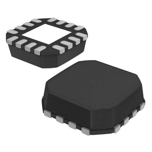
ICGOO电子元器件商城为您提供AD8659ACPZ-R7由Analog设计生产,在icgoo商城现货销售,并且可以通过原厂、代理商等渠道进行代购。 AD8659ACPZ-R7价格参考¥17.50-¥27.92。AnalogAD8659ACPZ-R7封装/规格:线性 - 放大器 - 仪表,运算放大器,缓冲器放大器, General Purpose Amplifier 4 Circuit Rail-to-Rail 16-LFCSP-WQ (4x4)。您可以下载AD8659ACPZ-R7参考资料、Datasheet数据手册功能说明书,资料中有AD8659ACPZ-R7 详细功能的应用电路图电压和使用方法及教程。
AD8659ACPZ-R7是Analog Devices Inc.推出的一款精密双通道运算放大器,属于线性放大器类别,适用于对精度、低噪声和低失调有较高要求的应用场景。该器件具有低输入偏置电流、低失调电压和轨到轨输出特性,工作电压范围宽(2.7V至5.5V),适合单电源或双电源系统。

典型应用场景包括:便携式医疗设备(如心电图仪、血糖仪)、工业传感器信号调理、高精度数据采集系统、电池供电仪器以及音频与通信前端电路。其低功耗和高精度特性使其在需要长期稳定运行的测量设备中表现优异。此外,AD8659ACPZ-R7也常用于光电二极管前置放大器、热电偶放大和应变桥放大等精密模拟信号处理场合。

由于采用紧凑的8引脚LFCSP封装,并具备良好的温度稳定性,该器件特别适用于空间受限且环境条件多变的嵌入式系统。整体而言,AD8659ACPZ-R7是一款适用于高精度、低功耗模拟信号放大的理想选择。
| 参数 | 数值 |
| -3db带宽 | - |
| 产品目录 | 集成电路 (IC) |
| 描述 | IC OPAMP GP 200KHZ RRO 16LFCSP |
| 产品分类 | Linear - Amplifiers - Instrumentation, OP Amps, Buffer Amps |
| 品牌 | Analog Devices Inc |
| 数据手册 | |
| 产品图片 | |
| 产品型号 | AD8659ACPZ-R7 |
| PCN组件/产地 | |
| rohs | 无铅 / 符合限制有害物质指令(RoHS)规范要求 |
| 产品系列 | - |
| 产品培训模块 | http://www.digikey.cn/PTM/IndividualPTM.page?site=cn&lang=zhs&ptm=30008http://www.digikey.cn/PTM/IndividualPTM.page?site=cn&lang=zhs&ptm=26202 |
| 供应商器件封装 | 16-LFCSP-WQ(4x4) |
| 其它名称 | AD8659ACPZ-R7CT |
| 包装 | 剪切带 (CT) |
| 压摆率 | 0.07 V/µs |
| 增益带宽积 | 200kHz |
| 安装类型 | 表面贴装 |
| 封装/外壳 | 16-WQFN 裸露焊盘,CSP |
| 工作温度 | -40°C ~ 125°C |
| 放大器类型 | 通用 |
| 标准包装 | 1 |
| 电压-电源,单/双 (±) | 2.7 V ~ 18 V, ±1.35 V ~ 9 V |
| 电压-输入失调 | 350µV |
| 电流-电源 | 18µA |
| 电流-输入偏置 | 5pA |
| 电流-输出/通道 | 12mA |
| 电路数 | 4 |
| 视频文件 | http://www.digikey.cn/classic/video.aspx?PlayerID=1364138032001&width=640&height=505&videoID=2245193153001 |
| 输出类型 | 满摆幅 |


- 商务部:美国ITC正式对集成电路等产品启动337调查
- 曝三星4nm工艺存在良率问题 高通将骁龙8 Gen1或转产台积电
- 太阳诱电将投资9.5亿元在常州建新厂生产MLCC 预计2023年完工
- 英特尔发布欧洲新工厂建设计划 深化IDM 2.0 战略
- 台积电先进制程称霸业界 有大客户加持明年业绩稳了
- 达到5530亿美元!SIA预计今年全球半导体销售额将创下新高
- 英特尔拟将自动驾驶子公司Mobileye上市 估值或超500亿美元
- 三星加码芯片和SET,合并消费电子和移动部门,撤换高东真等 CEO
- 三星电子宣布重大人事变动 还合并消费电子和移动部门
- 海关总署:前11个月进口集成电路产品价值2.52万亿元 增长14.8%


PDF Datasheet 数据手册内容提取
22 μA, RRIO, CMOS,18 V Operational Amplifiers Data Sheet AD8657/AD8659 FEATURES PIN CONNECTION DIAGRAMS Micropower at high voltage (18 V): 22 μA maximum OUT A 1 8 V+ Low offset voltage: 350 μV maximum –IN A 2 AD8657 7 OUT B TOP VIEW LGoawin i bnapnudt wbiiadst hcu prrroednut:c 2t:0 2 p3A0 mkHazx iamt uAmV = 100 typical +INV A– 34 (Not to Scale) 65 –+IINN BB 08804-001 Unity-gain crossover: 230 kHz Figure 1. AD8657 Pin Configuration, 8-Lead MSOP −3 dB closed-loop bandwidth: 305 kHz Single-supply operation: 2.7 V to 18 V OUT A 1 8 V+ Dual-supply operation: ±1.35 V to ±9 V –IN A 2 AD8657 7 OUT B TOP VIEW Unity-gain stable +IN A 3 (Not to Scale) 6 –IN B Excellent electromagnetic interference immunity V– 4 5 +IN B APoPrPtaLbIlCe AopTeIOraNtinSg systems N1 . O CLTEOEANSVNEE ICTT U TNHCEO ENXNPEOCSTEEDD.PADTO V– OR 08804-061 Figure 2. AD8657 Pin Configuration, 8-Lead LFCSP Current monitors 4 mA to 20 mA loop drivers Note: For AD8659 pin connections and for more information Buffer/level shifting about the pin connections for these products, see the Pin Multipole filters Configurations and Function Descriptions section. Remote/wireless sensors 60 Low power transimpedance amplifiers 50 GENERAL DESCRIPTION VSY = 2.7V VSY = 18V The AD8657/AD8659 are dual and quad micropower, precision, A) 40 rail-to-rail input/output amplifiers optimized for low power and MP (µ A 30 wide operating supply voltage range applications. ER P The AD8657/AD8659 operate from 2.7 V to 18 V with a typical I SY 20 quiescent supply current of 18 μA. The devices use the Analog 10 Devices, Inc., patented DigiTrim® trimming technique, which achieves low offset voltage. The AD8657/AD8659 also have 0 high immunity to electromagnetic interference. –50 –25 0 TEM2P5ERATUR5E0 (°C) 75 100 125 08804-023 The combination of low supply current, low offset voltage, very Figure 3. AD8657, Supply Current vs. Temperature low input bias current, wide supply range, and rail-to-rail input Table 1. Precision Micropower Op Amps (<250 μA) and output make the AD8657/AD8659 ideal for current Supply Voltage 5 V 12 V to 16 V 36 V monitoring in process and motor control applications. The Single AD8538 OP196 combination of precision specifications makes these devices AD8603 ideal for dc gain and buffering of sensor front ends or high ADA4051-1 impedance input sources in wireless or remote sensors or Dual AD8539 AD8657 AD8622 transmitters. AD8607 ADA4091-2 The AD8657/AD8659 are specified over the extended industrial ADA4051-2 ADA4096-2 temperature range (−40°C to +125°C). The AD8657 is available in Quad AD8609 AD8659 AD8624 an 8-lead MSOP package and an 8-lead LFCSP package; the ADA4091-4 AD8659 is available in a 14-lead SOIC package and 16-lead ADA4096-4 LFCSP package. Rev. C Information furnished by Analog Devices is believed to be accurate and reliable. However, no responsibility is assumed by Analog Devices for its use, nor for any infringements of patents or other One Technology Way, P.O. Box 9106, Norwood, MA 02062-9106, U.S.A. rights of third parties that may result from its use. Specifications subject to change without notice. No license is granted by implication or otherwise under any patent or patent rights of Analog Devices. Tel: 781.329.4700 www.analog.com Trademarks and registered trademarks are the property of their respective owners. Fax: 781.461.3113 ©2011–2017 Analog Devices, Inc. All rights reserved.
AD8657/AD8659 Data Sheet TABLE OF CONTENTS Features .............................................................................................. 1 Typical Performance Characteristics ..............................................9 Applications ....................................................................................... 1 Applications Information .............................................................. 19 General Description ......................................................................... 1 Input Stage ................................................................................... 19 Pin Connection Diagrams ............................................................... 1 Output Stage ................................................................................ 20 Revision History ............................................................................... 2 Rail to Rail ................................................................................... 20 Specifications ..................................................................................... 3 Resistive Load ............................................................................. 20 Electrical Characteristics—18 V Operation ............................. 3 Comparator Operation—AD8657 ........................................... 21 Electrical Characteristics—10 V Operation ............................. 4 EMI Rejection Ratio .................................................................. 22 Electrical Characteristics—2.7 V Operation ............................ 5 4 mA to 20 mA Process Control Current Loop Transmitter— Absolute Maximum Ratings ............................................................ 6 AD8657 ........................................................................................ 22 Thermal Resistance ...................................................................... 6 Outline Dimensions ....................................................................... 23 ESD Caution .................................................................................. 6 Ordering Guide .......................................................................... 24 Pin Configurations and Function Descriptions ........................... 7 REVISION HISTORY 6/2017—Rev. B to Rev. A Change to Inverting Op Amp Configuration Section Heading Change to 4 mA to 20 mA Process Control Current Loop and Changes to Figure 70 .............................................................. 20 Transmitter—AD8657 Section and Figure 78 ............................ 22 Change to Noninverting Op Amp Configuration Heading and Updated Outline Dimensions ....................................................... 24 Changes to Figure 71 ...................................................................... 20 Changes to Ordering Guide .......................................................... 24 Change to Comparator Operation—AD8657 Heading ............ 21 Change to 4 mA to 20 mA Process Control Current Loop 8/2012—Rev. A to Rev. B Transmitter—AD8657 Section Heading and Changed Added AD8659 ................................................................... Universal 33 μA to 34 μA ................................................................................ 22 Changes to Features Section............................................................ 1 Updated Outline Dimensions ....................................................... 24 Changes to Pin Connection Diagrams Section ............................ 1 Added Figure 81 and Figure 82 .................................................... 24 Added Figure 3, Renumbered Figures Sequentially ..................... 1 Changes to Ordering Guide .......................................................... 24 Changes to Table 1 ............................................................................ 1 Reordered Table 2 and Table 4 ........................................................ 3 3/2011—Rev. 0 to Rev. A Changes to Table 2 ............................................................................ 3 Added LFCSP Package Information ........................... Throughout Changes to Table 3 ............................................................................ 4 Added Figure 2, Renumbered Subsequent Figures .................... 1 Changes to Table 4 ............................................................................ 5 Changes to Table 2, Introductory Text; Input Characteristics, Changes to Table 6 ............................................................................ 6 Offset Voltage and Common-Mode Rejection Ratio Test Added Pin Configurations and Function Descriptions Section 7 Conditions/Comments; and Dynamic Performance, Phase Added Figure 4 and Figure 5 ........................................................... 7 Margin Values .................................................................................... 3 Added Table 7, Renumbered Tables Sequentially ........................ 7 Changes to Table 3, Introductory Text; Input Characteristics, Added Figure 6 and Figure 7 ........................................................... 8 Offset Voltage and Common-Mode Rejection Ratio Test Added Table 8 .................................................................................... 8 Conditions/Comments ..................................................................... 4 Changes to Figure 10 and Figure 13 ............................................... 9 Changes to Table 4, Introductory Text; Input Characteristics, Changes to Figure 14, Figure 15, Figure 17, and Figure 18 ....... 10 Offset Voltage and Common-Mode Rejection Ratio Test Changes to Figure 28 and Figure 31 ............................................. 12 Conditions/Comments ..................................................................... 5 Changes to Figure 32 ...................................................................... 13 Changes to Thermal Resistance Section and Table 5 ................... 6 Changes to Figure 39 ...................................................................... 14 Updated Outline Dimensions ....................................................... 21 Changes to Figure 63 and Figure 66 ............................................. 18 Changes to Ordering Guide .......................................................... 21 Moved Figure 68 ............................................................................. 19 1/2011—Revision 0: Initial Version Rev. C | Page 2 of 24
Data Sheet AD8657/AD8659 SPECIFICATIONS ELECTRICAL CHARACTERISTICS—18 V OPERATION V = 18 V, V = V /2 V, T = 25°C, unless otherwise specified. SY CM SY A Table 2. Parameter Symbol Test Conditions/Comments Min Typ Max Unit INPUT CHARACTERISTICS Offset Voltage V V = 0 V to 18 V 350 µV OS CM V = 0.3 V to 17.7 V, −40°C ≤ T ≤ +85°C 1.8 mV CM A V = 0.3 V to 17.7 V, −40°C ≤ T ≤ +125°C 2 mV CM A V = 0 V to 18 V, −40°C ≤ T ≤ +125°C 16 mV CM A Input Bias Current I 5 20 pA B −40°C ≤ T ≤ +125°C 2.9 nA A Input Offset Current I 40 pA OS −40°C ≤ T ≤ +125°C 5.8 nA A Input Voltage Range 0 18 V Common-Mode Rejection Ratio CMRR V = 0 V to 18 V 94 110 dB CM V = 0.3 V to 17.7 V, −40°C ≤ T ≤ +85°C 82 dB CM A V = 0.3 V to 17.7 V, −40°C ≤ T ≤ +125°C 80 dB CM A V = 0 V to 18 V, −40°C ≤ T ≤ +125°C 64 dB CM A Large Signal Voltage Gain A R = 100 kΩ, V = 0.5 V to 17.5 V 115 120 dB VO L O −40°C ≤ T ≤ +125°C 105 dB A Offset Voltage Drift ΔV /ΔT 2 μV/°C OS Input Resistance R 10 GΩ IN Input Capacitance, Differential Mode C 11 pF INDM Input Capacitance, Common Mode C 3.5 pF INCM OUTPUT CHARACTERISTICS Output Voltage High V R = 100 kΩ to V , −40°C ≤ T ≤ +125°C 17.97 V OH L CM A Output Voltage Low V R = 100 kΩ to V , −40°C ≤ T ≤ +125°C 30 mV OL L CM A Short-Circuit Current I ±12 mA SC Closed-Loop Output Impedance Z f = 1 kHz, A = 1 15 Ω OUT V POWER SUPPLY Power Supply Rejection Ratio PSRR V = 2.7 V to 18 V 100 115 dB SY −40°C ≤ T ≤ +125°C 90 dB A Supply Current per Amplifier I I = 0 mA 18 22 µA SY O −40°C ≤ T ≤ +125°C 34 µA A DYNAMIC PERFORMANCE Slew Rate SR R = 1 MΩ, C = 10 pF, A = 1 80 V/ms L L V Settling Time to 0.1% t V = 1 V step, R = 100 kΩ, C = 10 pF 15 µs S IN L L Unity-Gain Crossover UGC V = 10 mV p-p, R = 1 MΩ, C = 10 pF, A = 1 230 kHz IN L L V Phase Margin Φ V = 10 mV p-p, R = 1 MΩ, C = 10 pF, A = 1 60 Degrees M IN L L V Gain Bandwidth Product GBP V = 10 mV p-p, R = 1 MΩ, C = 10 pF, A = 100 230 kHz IN L L V −3 dB Closed-Loop Bandwidth f V = 10 mV p-p, R = 1 MΩ, C = 10 pF, A = 1 305 kHz −3 dB IN L L V Channel Separation CS f = 10 kHz, R = 1 MΩ 95 dB L EMI Rejection Ratio of +IN x EMIRR V = 100 mV ; f = 400 MHz, 900 MHz, 90 dB IN PEAK 1800 MHz, 2400 MHz NOISE PERFORMANCE Voltage Noise e p-p f = 0.1 Hz to 10 Hz 5 µV p-p n Voltage Noise Density e f = 1 kHz 50 nV/√Hz n f = 10 kHz 45 nV/√Hz Current Noise Density i f = 1 kHz 0.1 pA/√Hz n Rev. C | Page 3 of 24
AD8657/AD8659 Data Sheet ELECTRICAL CHARACTERISTICS—10 V OPERATION V = 10 V, V = V /2 V, T = 25°C, unless otherwise specified. SY CM SY A Table 3. Parameter Symbol Test Conditions/Comments Min Typ Max Unit INPUT CHARACTERISTICS Offset Voltage V V = 0 V to 10 V 350 µV OS CM V = 0.3 V to 9.7 V, −40°C ≤ T ≤ +85°C 1.6 mV CM A V = 0.3 V to 9.7 V, −40°C ≤ T ≤ +125°C 2 mV CM A V = 0 V to 10 V, −40°C ≤ T ≤ +125°C 16 mV CM A Input Bias Current I 2 15 pA B −40°C ≤ T ≤ +125°C 2.6 nA A Input Offset Current I 30 pA OS −40°C ≤ T ≤ +125°C 5.2 nA A Input Voltage Range 0 10 V Common-Mode Rejection Ratio CMRR V = 0 V to 10 V 88 105 dB CM V = 0.3 V to 9.7 V, −40°C ≤ T ≤ +85°C 76 dB CM A V = 0.3 V to 9.7 V, −40°C ≤ T ≤ +125°C 75 dB CM A V = 0 V to 10 V, −40°C ≤ T ≤ +125°C 59 dB CM A Large Signal Voltage Gain A R = 100 kΩ, V = 0.5 V to 9.5 V 108 120 dB VO L O −40°C ≤ T ≤ +125°C 100 dB A Offset Voltage Drift ΔV /ΔT 2 μV/°C OS Input Resistance R 10 GΩ IN Input Capacitance, Differential Mode C 11 pF INDM Input Capacitance, Common Mode C 3.5 pF INCM OUTPUT CHARACTERISTICS Output Voltage High V R = 100 kΩ to V , −40°C ≤ T ≤ +125°C 9.98 V OH L CM A Output Voltage Low V R = 100 kΩ to V , −40°C ≤ T ≤ +125°C 20 mV OL L CM A Short-Circuit Current I ±11 mA SC Closed-Loop Output Impedance Z f = 1 kHz, A = 1 15 Ω OUT V POWER SUPPLY Power Supply Rejection Ratio PSRR V = 2.7 V to 18 V 100 115 dB SY −40°C ≤ T ≤ +125°C 90 dB A Supply Current per Amplifier I I = 0 mA 18 22 µA SY O −40°C ≤ T ≤ +125°C 34 µA A DYNAMIC PERFORMANCE Slew Rate SR R = 1 MΩ, C = 10 pF, A = 1 75 V/ms L L V Settling Time to 0.1% t V = 1 V step, R = 100 kΩ, C = 10 pF 15 µs s IN L L Unity-Gain Crossover UGC V = 10 mV p-p, R = 1 MΩ, C = 10 pF, A = 1 225 kHz IN L L V Phase Margin Φ V = 10 mV p-p, R = 1 MΩ, C = 10 pF, A = 1 60 Degrees M IN L L V Gain Bandwidth Product GBP V = 10 mV p-p, R = 1 MΩ, C = 10 pF, A = 100 230 kHz IN L L V −3 dB Closed-Loop Bandwidth f V = 10 mV p-p, R = 1 MΩ, C = 10 pF, A = 1 300 kHz −3 dB IN L L V Channel Separation CS f = 10 kHz, R = 1 MΩ 95 dB L EMI Rejection Ratio of +IN x EMIRR V = 100 mV ; f = 400 MHz, 900 MHz, 90 dB IN PEAK 1800 MHz, 2400 MHz NOISE PERFORMANCE Voltage Noise e p-p f = 0.1 Hz to 10 Hz 5 µV p-p n Voltage Noise Density e f = 1 kHz 50 nV/√Hz n f = 10 kHz 45 nV/√Hz Current Noise Density i f = 1 kHz 0.1 pA/√Hz n Rev. C | Page 4 of 24
Data Sheet AD8657/AD8659 ELECTRICAL CHARACTERISTICS—2.7 V OPERATION V = 2.7 V, V = V /2 V, T = 25°C, unless otherwise specified. SY CM SY A Table 4. Parameter Symbol Test Conditions/Comments Min Typ Max Unit INPUT CHARACTERISTICS Offset Voltage V V = 0 V to 2.7 V 350 µV OS CM V = 0.3 V to 2.4 V, −40°C ≤ T ≤ +85°C 1.2 mV CM A V = 0.3 V to 2.4 V, −40°C ≤ T ≤ +125°C 2.5 mV CM A V = 0 V to 2.7 V, −40°C ≤ T ≤ +125°C 16 mV CM A Input Bias Current I 1 10 pA B −40°C ≤ T ≤ +125°C 2.6 nA A Input Offset Current I 20 pA OS −40°C ≤ T ≤ +125°C 5.2 nA A Input Voltage Range 0 2.7 V Common-Mode Rejection Ratio CMRR V = 0 V to 2.7 V 77 95 dB CM V = 0.3 V to 2.4 V, −40°C ≤ T ≤ +85°C 69 dB CM A V = 0.3 V to 2.4 V, −40°C ≤ T ≤ +125°C 62 dB CM A V = 0 V to 2.7 V, −40°C ≤ T ≤ +125°C 47 dB CM A Large Signal Voltage Gain A R = 100 kΩ, V = 0.5 V to 2.2 V 95 105 dB VO L O −40°C ≤ T ≤ +125°C 90 dB A Offset Voltage Drift ΔV /ΔT 2 μV/°C OS Input Resistance R 10 GΩ IN Input Capacitance, Differential Mode C 11 pF INDM Input Capacitance, Common Mode C 3.5 pF INCM OUTPUT CHARACTERISTICS Output Voltage High V R = 100 kΩ to V , −40°C ≤ T ≤ +125°C 2.69 V OH L CM A Output Voltage Low V R = 100 kΩ to V , −40°C ≤ T ≤ +125°C 10 mV OL L CM A Short-Circuit Current I ±4 mA SC Closed-Loop Output Impedance Z f = 1 kHz, A = 1 20 Ω OUT V POWER SUPPLY Power Supply Rejection Ratio PSRR V = 2.7 V to 18 V 100 115 dB SY −40°C ≤ T ≤ +125°C 90 dB A Supply Current per Amplifier I I = 0 mA 18 22 µA SY O −40°C ≤ T ≤ +125°C 34 µA A DYNAMIC PERFORMANCE Slew Rate SR R = 1 MΩ, C = 10 pF, A = 1 50 V/ms L L V Settling Time to 0.1% t V = 1 V step, R = 100 kΩ, C = 10 pF 20 µs s IN L L Unity-Gain Crossover UGC V = 10 mV p-p, R = 1 MΩ, C = 10 pF, A = 1 190 kHz IN L L V Phase Margin Φ V = 10 mV p-p, R = 1 MΩ, C = 10 pF, A = 1 55 Degrees M IN L L V Gain Bandwidth Product GBP V = 10 mV p-p, R = 1 MΩ, C = 10 pF, A = 100 200 kHz IN L L V −3 dB Closed-Loop Bandwidth f V = 10 mV p-p, R = 1 MΩ, C = 10 pF, A = 1 245 kHz −3 dB IN L L V Channel Separation CS f = 10 kHz, R = 1 MΩ 95 dB L EMI Rejection Ratio of +IN x EMIRR V = 100 mV ; f = 400 MHz, 900 MHz, 90 dB IN PEAK 1800 MHz, 2400 MHz NOISE PERFORMANCE Voltage Noise e p-p f = 0.1 Hz to 10 Hz 6 µV p-p n Voltage Noise Density e f = 1 kHz 60 nV/√Hz n f = 10 kHz 56 nV/√Hz Current Noise Density i f = 1 kHz 0.1 pA/√Hz n Rev. C | Page 5 of 24
AD8657/AD8659 Data Sheet ABSOLUTE MAXIMUM RATINGS THERMAL RESISTANCE Table 5. θ is specified for the worst-case conditions, that is, a device Parameter Rating JA soldered in a circuit board for surface-mount packages using a Supply Voltage 20.5 V standard 4-layer JEDEC board. The exposed pad (LFCSP Input Voltage (V−) − 300 mV to (V+) + 300 mV packages only) is soldered to the board. Input Current1 ±10 mA Differential Input Voltage ±V SY Table 6. Thermal Resistance Output Short-Circuit Indefinite Package Type θ θ Unit JA JC Duration to GND 8-Lead MSOP (RM-8) 142 45 °C/W Temperature Ranges 8-Lead LFCSP (CP-8-11) 75 12 °C/W Storage −65°C to +150°C 14-Lead SOIC (R-14) 115 36 °C/W Operating −40°C to +125°C 16-Lead LFCSP (CP-16-20) 52 13 °C/W Junction −65°C to +150°C Lead Temperature 300°C (Soldering, 60 sec) ESD CAUTION 1 The input pins have clamp diodes to the power supply pins. Limit the input current to 10 mA or less whenever input signals exceed the power supply rail by 0.3 V. Stresses at or above those listed under Absolute Maximum Ratings may cause permanent damage to the product. This is a stress rating only; functional operation of the product at these or any other conditions above those indicated in the operational section of this specification is not implied. Operation beyond the maximum operating conditions for extended periods may affect product reliability. Rev. C | Page 6 of 24
Data Sheet AD8657/AD8659 PIN CONFIGURATIONS AND FUNCTION DESCRIPTIONS OUT A 1 8 V+ OUT A 1 8 V+ AD8657 –IN A 2 7 OUT B –IN A 2 AD8657 7 OUT B TOP VIEW +INV A– 34 (Not to Scale) 65 –+IINN BB 08804-001 +INV A– 34 (NToOt Pto V SIEcWale) 65 –+IINN BB N1 . O CLTEOEANSVNEE ICTT U TNHCEO ENXNPEOCSTEEDD.PADTO V– OR 08804-061 Figure 4. AD8657 Pin Configuration, 8-Lead MSOP Figure 5. AD8657 Pin Configuration, 8-Lead LFCSP Table 7. Pin Function Descriptions, AD8657 Pin No.1 8-Lead MSOP 8-Lead LFCSP Mnemonic Description 1 1 OUT A Output Channel A. 2 2 −IN A Negative Input Channel A. 3 3 +IN A Positive Input Channel A. 4 4 V− Negative Supply Voltage. 5 5 +IN B Positive Input Channel B. 6 6 −IN B Negative Input Channel B. 7 7 OUT B Output Channel B. 8 8 V+ Positive Supply Voltage. N/A EP2 EPAD Exposed Pad. For the AD8657 (8-lead LFCSP only), connect the exposed pad to V− or leave it unconnected. 1 N/A means not applicable. 2 The exposed pad is not shown in the pin configuration diagram. Rev. C | Page 7 of 24
AD8657/AD8659 Data Sheet A D O–UINT AA 12 1143 O–IUNT D D NIC OUT OUT NC 6 5 4 3 +IN A 3 AD8659 12 +IN D 1 1 1 1 V+ 4 TOP VIEW 11 V– (Not to Scale) –IN A 1 12 –IN D +IN B 5 10 +IN C O–UINT BB 67 98 –OIUNT C C 08804-103 ++IINNV AB+ 342 (NAToOtD Pto8 V 6SIE5caW9le) 11910 +V+II–NN DC 5 6 7 8 B B C C N T T N –I OU OU –I NOTES 12 .. CNLOEICAN V=NE EN CIOTT IU NTNTHCEEOR ENNXNAPELO CCSTOEENDDN.PEACDTITOON V.– OR 08804-104 Figure 6. AD8659 Pin Configuration, 14-Lead SOIC_N Figure 7. AD8659 Pin Configuration, 16-Lead LFCSP Table 8. Pin Function Descriptions, AD8659 Pin No.1 14-Lead SOIC 16-Lead LFCSP Mnemonic Description 1 15 OUT A Output Channel A. 2 1 −IN A Negative Input Channel A. 3 2 +IN A Positive Input Channel A. 11 10 V− Negative Supply Voltage. 5 4 +IN B Positive Input Channel B. 6 5 −IN B Negative Input Channel B. 7 6 OUT B Output Channel B. 4 3 V+ Positive Supply Voltage. 8 7 OUT C Output Channel C. 9 8 −IN C Negative Input Channel C. 10 9 +IN C Positive Input Channel C. 12 11 +IN D Positive Input Channel D. 13 12 −IN D Negative Input Channel D. 14 14 OUT D Output Channel D. N/A 13 NIC No Internal Connection. N/A 16 NIC No Internal Connection. N/A EP2 EPAD2 Exposed Pad. For the AD8659 (16-lead LFCSP only), connect the exposed pad to V− or leave it unconnected. 1 N/A means not applicable. 2 The exposed pad is not shown in the pin configuration diagram. Rev. C | Page 8 of 24
Data Sheet AD8657/AD8659 TYPICAL PERFORMANCE CHARACTERISTICS T = 25°C, unless otherwise noted. A 160 160 140 VSY = 2.7V 140 VSY = 18V VCM = VSY/2 VCM = VSY/2 S 120 S 120 R R E E FI FI LI 100 LI 100 P P M M A A F 80 F 80 O O R R E 60 E 60 B B M M U U N 40 N 40 20 20 0 0 –140 –120 –100 –80 –60 –40 –20VOS0 (µV)20 40 60 80 100 120 140 08804-002 –140 –120 –100 –80 –60 –40 –20VOS0 (µV)20 40 60 80 100 120 140 08804-005 Figure 8. Input Offset Voltage Distribution Figure 11. Input Offset Voltage Distribution 18 20 16 VSY = 2.7V 18 VSY = 18V –40°C ≤ TA ≤ +125°C –40°C ≤ TA ≤ +125°C 16 14 S S ER ER14 FI12 FI PLI PLI12 M10 M A A F F10 O 8 O ER ER 8 MB 6 MB U U 6 N N 4 4 2 2 0 0 0 0.5 1.0 1.5 2.0 2.5T3C.V0OS3 .(5µV4/°.0C)4.5 5.0 5.5 6.0 6.5 7.0 08804-003 0 0.5 1.0 1.5 2.0 2.5T3C.V0OS3 .(5µV4/°.0C)4.5 5.0 5.5 6.0 6.5 7.0 08804-006 Figure 9. Input Offset Voltage Drift Distribution Figure 12. Input Offset Voltage Drift Distribution 350 350 VSY = 2.7V VSY = 18V 250 250 150 150 V) 50 V) 50 µ µ (S (S O O V –50 V –50 –150 –150 –250 –250 –3500 0.3 0.6 0.9 1.V2CM (V1).5 1.8 2.1 2.4 2.7 08804-207 –3500 2 4 6 8VCM (V1)0 12 14 16 18 08804-210 Figure 10. Input Offset Voltage vs. Common-Mode Voltage Figure 13. Input Offset Voltage vs. Common-Mode Voltage Rev. C | Page 9 of 24
AD8657/AD8659 Data Sheet 3.0 3.0 2.5 V–4S0Y°=C2≤.7TVA≤+85°C 2.5 V–4S0Y°=C1<8TVA<+85°C 2.0 2.0 1.5 1.5 1.0 1.0 V) 0.5 V) 0.5 m m (S 0 (S 0 O O V–0.5 V–0.5 –1.0 –1.0 –1.5 –1.5 –2.0 –2.0 –2.5 –2.5 –3.00 0.3 0.6 0.9 1.V2CM (V1).5 1.8 2.1 2.4 2.7 08804-211 –3.00 2 4 6 8VCM (V1)0 12 14 16 18 08804-214 Figure 14. Input Offset Voltage vs. Common-Mode Voltage Figure 17. Input Offset Voltage vs. Common-Mode Voltage 6 6 VSY = 2.7V VSY = 18V 4 –40°C ≤ TA ≤ +125°C 4 –40°C ≤ TA ≤ +125°C 2 2 V) V) m m (OS 0 (OS 0 V V –2 –2 –4 –4 –60 0.3 0.6 0.9 1.V2CM (V1).5 1.8 2.1 2.4 2.7 08804-212 –60 2 4 6 V8CM (V)10 12 14 16 18 08804-215 Figure 15. Input Offset Voltage vs. Common-Mode Voltage Figure 18. Input Offset Voltage vs. Common-Mode Voltage 10000 10000 VSY = 2.7V VSY = 18V 1000 1000 100 100 A) │IB+│ A) │IB+│ (pB │IB–│ (pB │IB–│ I I 10 10 1 1 0.1 0.1 25 50 TEMPERA75TURE (°C) 100 125 08804-008 25 50 TEMPERA75TURE (°C) 100 125 08804-011 Figure 16. Input Bias Current vs. Temperature Figure 19. Input Bias Current vs. Temperature Rev. C | Page 10 of 24
Data Sheet AD8657/AD8659 4 4 VSY = 2.7V VSY = 18V 3 3 2 2 1 1 A) A) (nB 0 (nB 0 I 125°C I 125°C –1 85°C –1 85°C 25°C 25°C –2 –2 –3 –3 –4 –4 0 0.3 0.6 0.9 1.V2CM (V1).5 1.8 2.1 2.4 2.7 08804-009 0 2 4 6 8VCM (V1)0 12 14 16 18 08804-012 Figure 20. Input Bias Current vs. Common-Mode Voltage Figure 23. Input Bias Current vs. Common-Mode Voltage 10 10 L (V)RAI 1 VSY = 2.7V RAIL (V) 1 VSY = 18V PLY PLY UP 100m –40°C UP 100m –40°C TO S ++2855°°CC TO S ++2855°°CC V)OH 10m +125°C V)OH 10m +125°C E ( E ( G G OLTA 1m OLTA 1m V V PUT 0.1m PUT 0.1m UT UT O O 0.01m0.001 0.01 LOA0D.1 CURRENT 1(mA) 10 100 08804-010 0.01m0.001 0.01 LOA0D.1 CURRENT 1(mA) 10 100 08804-013 Figure 21. Output Voltage (VOH) to Supply Rail vs. Load Current Figure 24. Output Voltage (VOH) to Supply Rail vs. Load Current 10 10 RAIL (V) 1 VSY = 2.7V RAIL (V) 1 VSY = 18V UPPLY 100m –40°C UPPLY 100m –40°C GE (V)TO SOL 10m +++281552°°5CC°C GE (V)TO SOL 10m +++281552°°5CC°C OLTA 1m OLTA 1m UTPUT V 0.1m UTPUT V 0.1m O O 0.01m0.001 0.01 LOA0D.1 CURRENT 1(mA) 10 100 08804-014 0.01m0.001 0.01 LOA0D.1 CURRENT 1(mA) 10 100 08804-017 Figure 22. Output Voltage (VOL) to Supply Rail vs. Load Current Figure 25. Output Voltage (VOL) to Supply Rail vs. Load Current Rev. C | Page 11 of 24
AD8657/AD8659 Data Sheet 2.700 18.000 RL = 1MΩ RL = 1MΩ 2.699 17.995 OUTPUT VOLTAGE, V (V)OH22..669978 RL = 100kΩ OUTPUT VOLTAGE, V (V)OH1177..998950 RL = 100kΩ 2.696 17.980 VSY = 2.7V VSY = 18V 2.695 17.975 –50 –25 0 TEM2P5ERATUR5E0 (°C) 75 100 125 08804-015 –50 –25 0 TEM2P5ERATUR50E (°C) 75 100 125 08804-018 Figure 26. Output Voltage (VOH) vs. Temperature Figure 29. Output Voltage (VOH) vs. Temperature 12 12 VSY = 2.7V VSY = 18V 10 10 RL = 100kΩ V) V) m m (OL 8 (OL 8 V V E, E, G G LTA 6 LTA 6 O O V V T T PU 4 PU 4 T T U U O RL = 100kΩ O 2 2 RL = 1MΩ RL = 1MΩ 0 0 –50 –25 0 TEMP25ERATUR5E0 (°C) 75 100 125 08804-016 –50 –25 0 TEMP25ERATUR5E0 (°C) 75 100 125 08804-019 Figure 27. Output Voltage (VOL) vs. Temperature Figure 30. Output Voltage (VOL) vs. Temperature 35 35 VSY = 2.7V VSY = 18V 30 30 25 25 A) A) µ µ P ( 20 P ( 20 M M A A R R PE 15 PE 15 Y Y S S I I 10 10 –40°C –40°C +25°C +25°C 5 +85°C 5 +85°C +125°C +125°C 00 0.3 0.6 0.9 1.V2CM (V1).5 1.8 2.1 2.4 2.7 08804-225 00 3 6 VC9M (V) 12 15 18 08804-228 Figure 28. Supply Current vs. Common-Mode Voltage Figure 31. Supply Current vs. Common-Mode Voltage Rev. C | Page 12 of 24
Data Sheet AD8657/AD8659 40 60 35 50 VSY = 2.7V 30 VSY = 18V A) A) 40 P (µ 25 P (µ M M A 20 A 30 R R E E P P I SY 15 I SY 20 10 –40°C 10 +25°C 5 +85°C +125°C 00 3 6 VSY9 (V) 12 15 18 08804-229 0–50 –25 0 TEMP25ERATUR5E0 (°C) 75 100 125 08804-023 Figure 32. Supply Current vs. Supply Voltage Figure 35. Supply Current vs. Temperature 60 135 40 PHASE VRSLY = = 1 M2.Ω7V 90 60 PHASE RVSLY = = 1 M18ΩV 135 40 90 B) OPEN-LOOP GAIN (d –22000 GAIN 04–545 PHASE (Degrees) PEN-LOOP GAIN (dB) –22000 GAIN 40–545 PHASE (Degrees) O CL = 10pF –40 CL = 100pF –90 –40 CL = 10pF –90 CL = 100pF –60 –135 1k 10kFREQUENCY (Hz)100k 1M 08804-021 –601k 10kFREQUENCY (Hz)100k 1M–135 08804-024 Figure 33. Open-Loop Gain and Phase vs. Frequency Figure 36. Open-Loop Gain and Phase vs. Frequency 60 60 VSY = 2.7V 40 AV = 100 40 AV = 100 VSY = 18V B) AIN (d 20 AV = 10 N (dB) 20 AV = 10 G AI LOOP 0 AV = 1 OOP G 0 AV = 1 D- L E D- LOS –20 OSE –20 C L C –40 –40 –60 100 1k FREQU1E0NkCY (Hz) 100k 1M 08804-022 –60100 1k FREQU1E0NkCY (Hz) 100k 1M 08804-025 Figure 34. Closed-Loop Gain vs. Frequency Figure 37. Closed-Loop Gain vs. Frequency Rev. C | Page 13 of 24
AD8657/AD8659 Data Sheet 1000 1000 AV = 100 AV = 100 AV = 10 AV = 10 100 100 Ω) AV = 1 Ω) AV = 1 (UT (UT O O Z Z 10 10 VSY = 2.7V VSY = 18V 1 100 1kFREQUENCY (Hz)10k 100k 08804-026 1 100 1kFREQUENCY (Hz)10k 100k 08804-029 Figure 38. Output Impedance vs. Frequency Figure 41. Output Impedance vs. Frequency 140 140 120 VVSCYM == 2V.S7YV/2 120 VVSCYM == 1V8SVY/2 100 100 R (dB) 80 R (dB) 80 R R CM 60 CM 60 40 40 20 20 0100 1k FREQU1E0NkCY (Hz) 100k 1M 08804-236 0100 1k FREQU1E0NkCY (Hz) 100k 1M 08804-030 Figure 39. CMRR vs. Frequency Figure 42. CMRR vs. Frequency 100 100 VSY = 2.7V VSY = 18V 80 80 PSRR (dB) 4600 PPSSRRRR+– PSRR (dB) 4600 PPSSRRRR+– 20 20 0 0 100 1k FREQU1E0NkCY (Hz) 100k 1M 08804-028 100 1k FREQU1E0NkCY (Hz) 100k 1M 08804-031 Figure 40. PSRR vs. Frequency Figure 43. PSRR vs. Frequency Rev. C | Page 14 of 24
Data Sheet AD8657/AD8659 70 70 60 VVSINY == 120.m7VV p-p OOSS+– 60 VVSINY == 1108mVV p-p OOSS+– RL = 1MΩ RL = 1MΩ 50 50 %) %) OT ( 40 OT ( 40 O O H H S S R 30 R 30 E E V V O O 20 20 10 10 0 0 10 CAPACIT1A00NCE (pF) 1000 08804-032 10 CAPACIT1A00NCE (pF) 1000 08804-035 Figure 44. Small Signal Overshoot vs. Load Capacitance Figure 47. Small Signal Overshoot vs. Load Capacitance VSY = ±1.35V CARVLL === 111M00ΩpF AVRSVLY == = 11 M±9ΩV V) CL = 100pF DI V) V/ DI m V/ OLTAGE (500 VOLTAGE (5 V TIME (100µs/DIV) 08804-033 TIME (100µs/DIV) 08804-036 Figure 45. Large Signal Transient Response Figure 48. Large Signal Transient Response CAVRSVLLY === = 111 M0±01Ωp.3F5V CAVRSVLLY === = 111 M0±09ΩpVF V) V) DI DI V/ V/ m m 5 5 E ( E ( G G A A T T L L O O V V TIME (100µs/DIV) 08804-034 TIME (100µs/DIV) 08804-037 Figure 46. Small Signal Transient Response Figure 49. Small Signal Transient Response Rev. C | Page 15 of 24
AD8657/AD8659 Data Sheet VSY = ±9V 0 AV = –10 INPUT INPUT RL = 1MΩ –0.2 0 E (V) –0.4 AVSVY = = – ±110.35 GE (V) E (V) –1 GE (V) AG RL = 1MΩ TA AG TA T L T L L O L –2 O O V O V T V UT T V UT U 2 P U 10 P P T P T N U N U I O I O 1 5 OUTPUT OUTPUT 0 0 TIME (40µs/DIV) 08804-039 TIME (40µs/DIV) 08804-042 Figure 50. Positive Overload Recovery Figure 53. Positive Overload Recovery VSY = ±9V 0.4 2 AV = –10 RL = 1MΩ 0.2 1 E (V) 0 INPUT GE (V) E (V) 0 INPUT GE (V) G A G A A T A T T L T L L O L O O V O V T V OUTPUT UT T V OUTPUT UT U 0 P U 0 P P T P T N U N U I VSY = ±1.35V O I O AV = –10 –1 –5 RL = 1MΩ –2 –10 TIME (40µs/DIV) 08804-038 TIME (40µs/DIV) 08804-041 Figure 51. Negative Overload Recovery Figure 54. Negative Overload Recovery INPUT INPUT DIV) VSY = 2.7V DIV) VSY = 18V V/ RL = 100kΩ V/ RL = 100kΩ 0m CL = 10pF 0m CL = 10pF 0 0 5 5 E ( E ( G G TA +5mV TA +5mV L L O O V V 0 0 ERROR BAND OUTPUT ERROR BAND OUTPUT –5mV –5mV TIME (10µs/DIV) 08804-040 TIME (10µs/DIV) 08804-043 Figure 52. Positive Settling Time to 0.1% Figure 55. Positive Settling Time to 0.1% Rev. C | Page 16 of 24
Data Sheet AD8657/AD8659 VSY = 2.7V VSY =18V RL = 100kΩ RL = 100kΩ CL = 10pF CL = 10pF V) V) DI INPUT DI INPUT V/ V/ m m 0 0 0 0 E (5 +5mV E (5 +5mV TAG OUTPUT 0 TAG OUTPUT 0 L L O ERROR BAND O ERROR BAND V V –5mV –5mV TIME (10µs/DIV) 08804-044 TIME (10µs/DIV) 08804-047 Figure 56. Negative Settling Time to 0.1% Figure 59. Negative Settling Time to 0.1% 1000 1000 VSY = 2.7V VSY = 18V Hz) Hz) √ √ V/ V/ n n Y ( 100 Y ( 100 T T SI SI N N E E D D E E S S OI OI N N E 10 E 10 G G A A T T L L O O V V 1 1 10 100 FR1kEQUENCY 1(H0kz) 100k 1M 08804-045 10 100 FR1kEQUENCY 1(H0kz) 100k 1M 08804-048 Figure 57. Voltage Noise Density vs. Frequency Figure 60. Voltage Noise Density vs. Frequency VSY = 2.7V VSY = 18V V) V) DI DI V/ V/ µ µ 2 2 E ( E ( G G A A T T L L O O V V TIME (2s/DIV) 08804-046 TIME (2s/DIV) 08804-049 Figure 58. 0.1 Hz to 10 Hz Noise Figure 61. 0.1 Hz to 10 Hz Noise Rev. C | Page 17 of 24
AD8657/AD8659 Data Sheet 3.0 20 VSY = 2.7V 18 VSY = 18V 2.5 VIN = 2.6V VIN = 17.9V RL = 1MΩ 16 RL = 1MΩ AV = 1 AV = 1 NG (V)2.0 NG (V)1124 WI WI UT S1.5 UT S10 UTP UTP 8 O1.0 O 6 4 0.5 2 0 0 10 100 FR1kEQUENCY 1(H0kz) 100k 1M 08804-050 10 100 FR1kEQUENCY 1(H0kz) 100k 1M 08804-053 Figure 62. Output Swing vs. Frequency Figure 65. Output Swing vs. Frequency 10 100 VSY=18V VIN=0.2VRMS VSY=2.7V 10 RL=1MΩ VIN=0.2VRMS AV= 1 RL=1MΩ %) 1 AV= 1 %) 1 N ( N ( + + D D H H T T 0.1 0.1 0.01 0.0110 100 FREQUE1NkCY (Hz) 10k 100k 08804-260 0.00110 100 FREQUE1NkCY (Hz) 10k 100k 08804-263 Figure 63. THD + N vs. Frequency Figure 66. THD + N vs. Frequency 0 0 1MΩ 1MΩ –20 VRSLY = = 1 M2.Ω7V 10kΩ –20 VRSLY = = 1 M18ΩV 10kΩ N (dB) –40 AV = –100 RL N (dB) –40 AV = –100 RL O O ARATI –60 ARATI –60 VVIINN == 15VV pp--pp EP VIN = 0.5V p-p EP VIN = 10V p-p L S –80 VIN = 1.5V p-p L S –80 VIN = 15V p-p NE VIN = 2.6V p-p NE VIN = 17V p-p N N A–100 A–100 H H C C –120 –120 –140 –140 100 1kFREQUENCY (Hz)10k 100k 08804-052 100 1kFREQUENCY (Hz)10k 100k 08804-055 Figure 64. Channel Separation vs. Frequency Figure 67. Channel Separation vs. Frequency Rev. C | Page 18 of 24
Data Sheet AD8657/AD8659 APPLICATIONS INFORMATION V+ VB1 I1 M8 M9 M5 M10 M11 M3 M4 +IN x R1 M16 D1 D2 VB2 OUT x –IN x R2 M1 M2 M17 M12 M13 V– M7 M6 M14 M15 08804-056 Figure 68. Simplified Schematic The AD8657/AD8659 are low power, rail-to-rail input and output These changes are a result of the load transistors (M8, M9, M14, precision CMOS amplifiers that operate over a wide supply and M15) running out of headroom. As the load transistors are voltage range of 2.7 V to 18 V. The AD8657/AD8659 use the forced into the triode region of operation, the mismatch of their Analog Devices DigiTrim technique to achieve a higher degree drain impedances contributes to the offset voltage of the amplifier. of precision than is available from other CMOS amplifiers. The This problem is exacerbated at high temperatures due to the DigiTrim technique is a method of trimming the offset voltage decrease in the threshold voltage of the input transistors (see of an amplifier after assembly. The advantage of post-package Figure 14, Figure 15, Figure 17, and Figure 18 for typical perfor- trimming is that it corrects any shifts in offset voltage caused by mance data). mechanical stresses of assembly. Current Source I1 drives the PMOS transistor pair. As the input The AD8657/AD8659 also employ unique input and output common-mode voltage approaches the upper rail, I1 is steered stages to achieve a rail-to-rail input and output range with a away from the PMOS differential pair through the M5 transistor. very low supply current. The bias voltage, VB1 (see Figure 68), controls the point where this transfer occurs. M5 diverts the tail current into a current mirror INPUT STAGE consisting of the M6 and M7 transistors. The output of the current Figure 68 shows the simplified schematic of the AD8657/AD8659. mirror then drives the NMOS pair. Note that the activation of The input stage comprises two differential transistor pairs, an this current mirror causes a slight increase in supply current at NMOS pair (M1, M2) and a PMOS pair (M3, M4). The input high common-mode voltages (see Figure 28 and Figure 31 for common-mode voltage determines which differential pair turns more details). on and is more active than the other. The AD8657/AD8659 achieve their high performance by using The PMOS differential pair is active when the input voltage low voltage MOS devices for their differential inputs. These low approaches and reaches the lower supply rail. The NMOS pair voltage MOS devices offer excellent noise and bandwidth per is needed for input voltages up to and including the upper supply unit of current. Each differential input pair is protected by proprie- rail. This topology allows the amplifier to maintain a wide tary regulation circuitry (not shown in the simplified schematic). dynamic input voltage range and to maximize signal swing to The regulation circuitry consists of a combination of active both supply rails. devices that maintain the proper voltages across the input pairs For the majority of the input common-mode voltage range, the during normal operation and passive clamping devices that protect PMOS differential pair is active. Differential pairs commonly the amplifier during fast transients. However, these passive exhibit different offset voltages. The handoff from one pair to the clamping devices begin to forward bias as the common-mode other creates a step-like characteristic that is visible in the V vs. voltage approaches either power supply rail, thereby causing an OS V graphs (see Figure 10 and Figure 13). This characteristic is increase in the input bias current (see Figure 20 and Figure 23). CM inherent in all rail-to-rail amplifiers that use the dual differential The input devices are also protected from large differential pair topology. Therefore, always choose a common-mode voltage input voltages by clamp diodes (D1 and D2). These diodes are that does not include the region of handoff from one input buffered from the inputs with two 10 kΩ resistors (R1 and R2). differential pair to the other. The differential diodes turn on whenever the differential voltage Additional steps in the V vs. V curves are also visible as the exceeds approximately 600 mV; in this condition, the differential OS CM input common-mode voltage approaches the power supply rails. input resistance drops to 20 kΩ. Rev. C | Page 19 of 24
AD8657/AD8659 Data Sheet OUTPUT STAGE Inverting Op Amp Configuration The AD8657/AD8659 feature a complementary output stage Figure 70 shows the AD8657/AD8659 in an inverting configu- consisting of the M16 and M17 transistors. These transistors are ration with a resistive load, RL, at the output. The actual load configured in Class AB topology and are biased by the voltage seen by the amplifier is the parallel combination of the feedback source, VB2. This topology allows the output voltage to go resistor, R2, and load, RL. For example, the combination of a feed- within millivolts of the supply rails, achieving a rail-to-rail output back resistor of 1 kΩ and a load of 1 MΩ results in an equivalent swing. The output voltage is limited by the output impedance of the load resistance of 999 Ω at the output. Because the AD8657/ transistors, which are low R MOS devices. The output voltage AD8659 are incapable of driving such a heavy load, performance ON swing is a function of the load current and can be estimated using degrades greatly. the output voltage to the supply rail vs. load current diagrams (see To avoid loading the output, use a larger feedback resistor, but Figure 21, Figure 22, Figure 24, and Figure 25). consider the resistor thermal noise effect on the overall circuit. RAIL TO RAIL R2 The AD8657/AD8659 feature rail-to-rail input and output with +VSY a supply voltage from 2.7 V to 18 V. Figure 69 shows the input R1 and output waveforms of the AD8657/AD8659 configured as a VIN unity-gain buffer with a supply voltage of ±9 V and a resistive AADD88665579/ VOUT load of 1 MΩ. With an input voltage of ±9 V, the AD8657/AD8659 RL allow the output to swing very close to both rails. Additionally, they do not exhibit phase reversal. RL, EFF– =V SRYL||R2 08804-058 INPUT VSY = ±9V Figure 70. Inverting Op Amp Configuration OUTPUT RL = 1MΩ Noninverting Op Amp Configuration Figure 71 shows the AD8657/AD8659 in a noninverting configu- V) DI ration with a resistive load, R, at the output. The actual load seen V/ L E (5 by the amplifier is the parallel combination of R1 + R2 and RL. G TA R2 L O V +VSY R1 AD8657/ TIME (200µs/DIV) 08804-057 VIN AD8659 VROLUT RESISTIVE LOFigAuDre 69. Rail-to-Rail Input and Output RL, EFF = –RVLS|Y| (R1 + R2) 08804-059 Figure 71. Noninverting Op Amp Configuration The feedback resistor alters the load resistance that an amplifier sees. It is, therefore, important to be aware of the value of feed- back resistors chosen for use with the AD8657/AD8659. The amplifiers are capable of driving resistive loads down to 100 kΩ. The following two examples, inverting and noninverting configurations, show how the feedback resistor changes the actual load resistance seen at the output of the amplifier. Rev. C | Page 20 of 24
Data Sheet AD8657/AD8659 COMPARATOR OPERATION—AD8657 These diodes consist of substrate PNP bipolar transistors, and conduct whenever the differential input voltage exceeds approxi- An op amp is designed to operate in a closed-loop configuration mately 600 mV; however, these diodes also allow a current path with feedback from its output to its inverting input. Figure 72 from the input to the lower supply rail, thus resulting in an shows the AD8657 configured as a voltage follower with an input increase in the total supply current of the system. As shown in voltage that is always kept at midpoint of the power supplies. Figure 76, both configurations yield the same result. At 18 V of The same configuration is applied to the unused channel. A1 and power supply, I + remains at 36 μA per dual amplifier, but I − A2 indicate the placement of ammeters to measure supply current. SY SY increases to 140 μA in magnitude per dual amplifier. I + refers to the current flowing from the upper supply rail to SY the op amp, and ISY− refers to the current flowing from the op +VSY amp to the lower supply rail. As shown in Figure 73, as expected in normal operating condition, the total current flowing into the op amp is equivalent to the total current flowing out of the op amp, 100kΩ A1 ISY+ where, I + = I − = 36 μA for the dual AD8657 at V = 18 V. SY SY SY +VSY AD8657 VOUT 1/2 A1 ISY+ 100kΩ A2 ISY– 100kΩ AD18/2657 VOUT –VSY 08804-068 Figure 74. Comparator A +VSY 100kΩ A2 ISY– –VSY 08804-066 A1 ISY+ Figure 72. Voltage Follower 100kΩ AD8657 40 1/2 VOUT 35 A) 100kΩ A2 ISY– µ 30 R ( E AMPLIFI 2205 –VSY 08804-069 L Figure 75. Comparator B A U R D 15 160 E PSY 10 IISSYY+– 140 I 5 µA) 120 R ( E 0 0 2 4 6 V8SY (V)10 12 14 16 18 08804-067 AMPLIFI 10800 ISY– Figure 73. Supply Current vs. Supply Voltage (Voltage Follower) AL ISY+ U D 60 In contrast to op amps, comparators are designed to work in an R E p open-loop configuration and to drive logic circuits. Although Y 40 S I op amps are different from comparators, occasionally an unused 20 section of a dual op amp is used as a comparator to save board space and cost; however, this is not recommended. 0 Figure 74 and Figure 75 show the AD8657 configured as a com- 0 2 4 6 8VSY (V1)0 12 14 16 18 08804-070 parator, with 100 kΩ resistors in series with the input pins. Any Figure 76. Supply Current vs. Supply Voltage (AD8657 as a Comparator) unused channels are configured as buffers with the input voltage kept at the midpoint of the power supplies. The AD8657/AD8659 have input devices that are protected from large differential input voltages by Diode D1 and Diode D2 (refer to Figure 68). Rev. C | Page 21 of 24
AD8657/AD8659 Data Sheet Note that 100 kΩ resistors are used in series with the input of The transmitter powers directly from the control loop power the op amp. If smaller resistor values are used, the supply current of supply, and the current in the loop carries signal from 4 mA to the system increases much more. For more details on op amps as 20 mA. Thus, 4 mA establishes the baseline current budget within comparators, refer to the AN-849 Application Note Using Op which the circuit must operate. Using the AD8657 is an excellent Amps as Comparators. choice due to its low supply current of 34 μA per amplifier over temperature and supply voltage. The current transmitter controls EMI REJECTION RATIO the current flowing in the loop, where a zero-scale input signal Circuit performance is often adversely affected by high frequency is represented by 4 mA of current and a full-scale input signal electromagnetic interference (EMI). In the event where signal is represented by 20 mA. The transmitter also floats from the strength is low and transmission lines are long, an op amp must control loop power supply, V , while signal ground is in the DD accurately amplify the input signals. However, all op amp pins— receiver. The loop current is measured at the load resistor, R, L the noninverting input, inverting input, positive supply, negative at the receiver side. supply, and output pins—are susceptible to EMI signals. These At a zero-scale input, a current of V /R flows through R´. high frequency signals are coupled into an op amp by various REF NULL This creates a current flowing through the sense resistor, I , means such as conduction, near field radiation, or far field radi- SENSE determined by the following equation (see Figure 78 for details): ation. For example, wires and PCB traces can act as antennas and pick up high frequency EMI signals. ISENSE, MIN = (VREF × R´)/(RNULL × RSENSE) Precision op amps, such as the AD8657 and AD8659, do not With a full-scale input voltage, current flowing through R´ is amplify EMI or RF signals because of their relatively low increased by the full-scale change in VIN/RSPAN. This creates an bandwidth. However, due to the nonlinearities of the input increase in the current flowing through the sense resistor. devices, op amps can rectify these out-of-band signals. When I = (Full-Scale Change in V × R´)/(R × R ) SENSE, DELTA IN SPAN SENSE these high frequency signals are rectified, they appear as a dc Therefore offset at the output. I = I + I To describe the ability of the AD8657/AD8659 to perform as SENSE, MAX SENSE, MIN SENSE, DELTA intended in the presence of an electromagnetic energy, the When R´ >> RSENSE, the current through the load resistor at the electromagnetic interference rejection ratio (EMIRR) of the receiver side is almost equivalent to ISENSE. noninverting pin is specified in Table 2, Table 3, and Table 4 of Figure 78 is designed for a full-scale input voltage of 5 V. At 0 V the Specifications section. A mathematical method of of input, loop current is 3.5 mA; and at a full scale of 5 V, the measuring EMIRR is defined as follows: loop current is 21 mA. This allows software calibration to fine EMIRR = 20 log (V /ΔV ) tune the current loop to the 4 mA to 20 mA range. IN_PEAK OS 140 The AD8657 and ADR3550 both consume only 160 μA quiescent current, making 3.34 mA current available to power additional 120 signal conditioning circuitry or to power a bridge circuit. 100 VREF VAODURT35V5IN0 B) GND R (d 80 RN1UMLΩL 10CµF2 0.1CµF3 C0.41µF C105µF MIR 1% E 60 RSPAN 200kΩ 1/2 VIN 1% AD8657 Q1 240010M VVISNY ==F 1i2g0.u07mVr1e0VT 07OPM7EF 1A.R 8KEEVMQIURERN vCsY. F (rHezq)u1Gency 10G 08804-071 0V TO 5V 62811kkRR%%ΩΩ21 R1.32kΩ 39C01pF 3.R3k4ΩRS1E0ND0SΩ1E 240TmmOAA V1R18D0VDL0Ω 1% 4 mA TO 20 mA PROCESS CONTROL CURRENT LOOP TRANSMITTER—AD8657 N1.O RT1E +S R2 = R´. 08804-060 The 2-wire current transmitters are often used in distributed Figure 78. 4 mA to 20 mA Current Loop Transmitter control systems and process control applications to transmit analog signals between sensors and process controllers. Figure 78 shows a 4 mA to 20 mA current loop transmitter. Rev. C | Page 22 of 24
Data Sheet AD8657/AD8659 OUTLINE DIMENSIONS 3.20 3.00 2.80 8 5 5.15 3.20 4.90 3.00 4.65 2.80 1 4 PIN 1 IDENTIFIER 0.65 BSC 0.95 15° MAX 0.85 1.10 MAX 0.75 0.80 0.15 0.40 6° 0.23 0.55 CO0P.0L50A.1N0ARICTOYMPLIANT0. 2T5O JEDEC STA0°NDARDS 0M.0O9-187-AA 0.40 10-07-2009-B Figure 79. 8-Lead Mini Small Outline Package [MSOP] (RM-8) Dimensions shown in millimeters DETAIL A (JEDEC 95) 2.44 3.10 2.34 3.00 SQ 2.24 2.90 0.50 BSC 5 8 PIN 1 INDEX 1.70 AREA EXPPAODSED 1.60 0.50 1.50 0.40 4 11 0.30 0.20 MIN TOP VIEW BOTTOM VIEW PIN 1 INDICATOR AREA OPTIONS (SEE DETAIL A) 0.80 0.75 SIDE VIEW 0.05 MAX FTOHER EPXRPOOPSEERD C POANDN, ERCETFIEORN TOOF 0.70 0.02 NOM THE PIN CONFIGURATION AND COPLANARITY FUNCTION DESCRIPTIONS SEATING 0.30 0.08 SECTION OF THIS DATA SHEET PKG-005136 PLANE CO00..M2250PLIANTTOJEDEC S0.T2A0N3 DRAERFDS MO-229-W3030D-4 02-10-2017-C Figure 80. 8-Lead Lead Frame Chip Scale Package [LFCSP] 3 mm × 3 mm Body and 0.75 mm Package Height (CP-8-11) Dimensions shown in millimeters Rev. C | Page 23 of 24
AD8657/AD8659 Data Sheet 8.75 (0.3445) 8.55 (0.3366) 4.00 (0.1575) 14 8 6.20 (0.2441) 3.80 (0.1496) 1 7 5.80 (0.2283) 1.27 (0.0500) 0.50 (0.0197) BSC 45° 1.75 (0.0689) 0.25 (0.0098) 0.25 (0.0098) 1.35 (0.0531) 8° 0.10 (0.0039) 0° COPLANARITY SEATING 0.10 0.51 (0.0201) PLANE 0.25 (0.0098) 1.27 (0.0500) 0.31 (0.0122) 0.17 (0.0067) 0.40 (0.0157) COMPLIANTTO JEDEC STANDARDS MS-012-AB C(RINOEFNPETARRREOENNLCLTEIHN EOGSN EDLSIYM)AEANNRDSEI AORRNOESU NANORDEET DAIN-PO MPFRIFLO LMPIIMRLELIATIMTEEER TFSEO; RIRN ECUQHSU EDI VIINMA LEDENENSSTIIOGSN NFS.OR 060606-A Figure 81. 14-Lead Standard Small Outline Package [SOIC_N] Narrow Body (R-14) Dimensions shown in millimeters and (inches) DETAIL A (JEDEC 95) 4.10 0.35 4.00 SQ 0.30 PIN 1 3.90 0.25 INDICATOR PIN 1 0.65 13 16 (INSEDEIC DAETTAOIRL AAR)EA OPTIONS BSC 12 11 2.70 EXPPAODSED 2.60 SQ 2.50 4 9 0.45 8 5 0.20 MIN TOP VIEW 0.40 BOTTOM VIEW 0.35 0.80 FOR PROPER CONNECTION OF 0.75 SIDE VIEW 0.05 MAX THE EXPOSED PAD, REFER TO 0.70 THE PIN CONFIGURATION AND 0.02 NOM FUNCTION DESCRIPTIONS COPLANARITY SECTION OF THIS DATA SHEET. SEATING 0.08 PLANE 0.20 REF PKG-004828 COMPLIANTTOJEDEC STANDARDS MO-220-WGGC. 02-22-2017-C Figure 82. 16-Lead Lead Frame Chip Scale Package [LFCSP] 4 mm × 4 mm Body and 0.75 mm Package Height (CP-16-17) Dimensions shown in millimeters ORDERING GUIDE Model1 Temperature Range Package Description Package Option Branding AD8657ARMZ −40°C to +125°C 8-Lead Mini Small Outline Package [MSOP] RM-8 A2N AD8657ARMZ-R7 −40°C to +125°C 8-Lead Mini Small Outline Package [MSOP] RM-8 A2N AD8657ARMZ-RL −40°C to +125°C 8-Lead Mini Small Outline Package [MSOP] RM-8 A2N AD8657ACPZ-R7 −40°C to +125°C 8-Lead Lead Frame Chip Scale Package [LFCSP] CP-8-11 A2N AD8657ACPZ-RL −40°C to +125°C 8-Lead Lead Frame Chip Scale Package [LFCSP] CP-8-11 A2N AD8659ARZ −40°C to +125°C 14-Lead Standard Small Outline Package [SOIC_N] R-14 AD8659ARZ-R7 −40°C to +125°C 14-Lead Standard Small Outline Package [SOIC_N] R-14 AD8659ARZ-RL −40°C to +125°C 14-Lead Standard Small Outline Package [SOIC_N] R-14 AD8659ACPZ-R7 −40°C to +125°C 16-Lead Lead Frame Chip Scale Package [LFCSP] CP-16-17 AD8659ACPZ-RL −40°C to +125°C 16-Lead Lead Frame Chip Scale Package [LFCSP] CP-16-17 1 Z = RoHS Compliant Part. ©2011–2017 Analog Devices, Inc. All rights reserved. Trademarks and registered trademarks are the property of their respective owners. D08804-0-6/17(C) Rev. C | Page 24 of 24