ICGOO在线商城 > 集成电路(IC) > 线性 - 放大器 - 仪表,运算放大器,缓冲器放大器 > TSV994AIYPT
 Datasheet下载
- 型号: TSV994AIYPT
- 制造商: STMicroelectronics
- 库位|库存: xxxx|xxxx
- 要求:
| 数量阶梯 | 香港交货 | 国内含税 |
| +xxxx | $xxxx | ¥xxxx |
查看当月历史价格
查看今年历史价格
TSV994AIYPT产品简介:
ICGOO电子元器件商城为您提供TSV994AIYPT由STMicroelectronics设计生产,在icgoo商城现货销售,并且可以通过原厂、代理商等渠道进行代购。 TSV994AIYPT价格参考。STMicroelectronicsTSV994AIYPT封装/规格:线性 - 放大器 - 仪表,运算放大器,缓冲器放大器, 通用 放大器 4 电路 满摆幅 14-TSSOP。您可以下载TSV994AIYPT参考资料、Datasheet数据手册功能说明书,资料中有TSV994AIYPT 详细功能的应用电路图电压和使用方法及教程。
TSV994AIYPT 是由 STMicroelectronics(意法半导体)生产的一款高性能运算放大器,属于线性放大器中的仪表、运算及缓冲放大器类别。以下是其典型应用场景:

 1. 工业自动化与控制
   - 传感器信号放大:TSV994AIYPT 具有低噪声和高增益带宽积(7 MHz),适合用于放大来自压力、温度或位置传感器的微弱信号。
   - 电机驱动反馈回路:在工业电机控制系统中,该运放可用于电流或电压反馈信号的精确处理。

 2. 消费电子
   - 音频信号处理:由于其低失真特性,TSV994AIYPT 可用于便携式音频设备(如耳机放大器或音响系统)中的信号放大。
   - 触摸屏控制器:在触控屏应用中,这款运放可以增强电容式触摸传感器的信号灵敏度。

 3. 医疗设备
   - 生物电信号采集:例如心电图(ECG)、脑电图(EEG)等设备中,TSV994AIYPT 的低输入偏置电流和轨到轨输出特性使其非常适合放大微弱的生物电信号。
   - 超声波成像:作为前端信号调理电路的一部分,用于放大超声探头接收到的弱信号。

 4. 汽车电子
   - 车载信息娱乐系统:可用于音频信号的放大和处理,提升音质表现。
   - ADAS(高级驾驶辅助系统):在摄像头模块或雷达系统中,用于信号调理以提高检测精度。

 5. 通信设备
   - 射频前端信号调理:TSV994AIYPT 的高速性能和低功耗特点使其适用于无线通信模块中的信号预处理。
   - 数据转换接口:在 ADC/DAC 系统中用作缓冲放大器,确保信号完整性。

 6. 测试与测量
   - 精密仪器:如数字万用表、示波器等,利用其高精度和稳定性进行信号放大和测量。
   - 电源监控:在电源管理单元中,用于监测和调节输出电压或电流。

总之,TSV994AIYPT 凭借其出色的电气性能(低噪声、低功耗、高带宽)和小型化的 SOIC-8 封装设计,广泛适用于需要高精度和低功耗的各类应用场合。
| 参数 | 数值 |
| -3db带宽 | - |
| 产品目录 | 集成电路 (IC) |
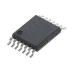
| 描述 | IC OPAMP GP 20MHZ RRO 14TSSOP |
| 产品分类 | Linear - Amplifiers - Instrumentation, OP Amps, Buffer Amps |
| 品牌 | STMicroelectronics |
| 数据手册 | |
| 产品图片 |
|
| 产品型号 | TSV994AIYPT |
| rohs | 无铅 / 符合限制有害物质指令(RoHS)规范要求 |
| 产品系列 | Q 汽车 |
| 供应商器件封装 | 14-TSSOP |
| 其它名称 | 497-10825-1 |
| 其它有关文件 | http://www.st.com/web/catalog/sense_power/FM123/SC61/SS1613/LN1591/PF247558?referrer=70071840http://www.st.com/web/catalog/sense_power/FM123/SC61/SS1613/LN1592/PF247558?referrer=70071840 |
| 包装 | 剪切带 (CT) |
| 压摆率 | 10 V/µs |
| 增益带宽积 | 20MHz |
| 安装类型 | 表面贴装 |
| 封装/外壳 | 14-TSSOP(0.173",4.40mm 宽) |
| 工作温度 | -40°C ~ 125°C |
| 放大器类型 | 通用 |
| 标准包装 | 1 |
| 电压-电源,单/双 (±) | 2.5 V ~ 5.5 V |
| 电压-输入失调 | - |
| 电流-电源 | 820µA |
| 电流-输入偏置 | 1pA |
| 电流-输出/通道 | 35mA |
| 电路数 | 4 |
| 输出类型 | 满摆幅 |


- 商务部:美国ITC正式对集成电路等产品启动337调查
- 曝三星4nm工艺存在良率问题 高通将骁龙8 Gen1或转产台积电
- 太阳诱电将投资9.5亿元在常州建新厂生产MLCC 预计2023年完工
- 英特尔发布欧洲新工厂建设计划 深化IDM 2.0 战略
- 台积电先进制程称霸业界 有大客户加持明年业绩稳了
- 达到5530亿美元!SIA预计今年全球半导体销售额将创下新高
- 英特尔拟将自动驾驶子公司Mobileye上市 估值或超500亿美元
- 三星加码芯片和SET,合并消费电子和移动部门,撤换高东真等 CEO
- 三星电子宣布重大人事变动 还合并消费电子和移动部门
- 海关总署:前11个月进口集成电路产品价值2.52万亿元 增长14.8%


PDF Datasheet 数据手册内容提取
TSV991, TSV992, TSV994 TSV991A TSV992A, TSV994A Datasheet Rail-to-rail input/output 20 MHz GBP operational amplifiers Features Pinconnections (topview) • Low input offset voltage: 1.5 mV max. (A grade) SOT23-5 DDFFNN8822xx22 • Rail-to-rail input and output • Wide bandwidth 20 MHz • Stable for gain ≥ 4 or ≤ -3 • Low power consumption: 820 µA typ. • High output current: 35 mA DFN61.3x1.6x0.55 • Operating from 2.5 V to 5.5 V MiniSO8,SO8, DFN8 2x2 • Low input bias current, 1 pA typ. IN-1 6 VCC+ • ESD internal protection ≥ 5 kV IN+2 5 VCC- NC3 4 OUT Applications SO14,TSSOP14 • Battery-powered applications • Portable devices • Signal conditioning and active filtering • Medical instrumentation • Automotive applications Description The TSV99x and TSV99xA family of single, dual, and quad operational amplifiers Product status link offers low voltage operation and rail-to-rail input and output. These devices feature an excellent speed/power consumption ratio, offering a 20 MHz gain-bandwidth, TSV991, TSV992, TSV994, TSV991A, stable for gains above 4 (100 pF capacitive load), while consuming only 1.1 mA TSV992A, TSV994A maximum at 5 V. They also feature an ultra-low input bias current. These Related products characteristics make the TSV99x family ideal for sensor interfaces, battery-supplied and portable applications, as well as active filtering. These characteristics make the See For unity-gain TSV99x, TSV99xA family ideal for sensor interfaces, battery-supplied and portable TSV991,TSV992, stable amplifiers applications, as well as active filtering. TSV994 DS4975 - Rev 13 - April 2018 www.st.com For further information contact your local STMicroelectronics sales office.
TSV991, TSV992, TSV994 TSV991A, TSV992A, TSV994A Absolute maximum ratings and operating conditions 1 Absolute maximum ratings and operating conditions Table 1. Absolute maximum ratings (AMR) Symbol Parameter Value Unit VCC Supply voltage (1) 6 Vid Differential input voltage (2) ±VCC V Vin Input voltage (3) (VCC-) - 0.2 to (VCC+) + 0.2 Iin Input current (4) 10 mA Tstg Storage temperature -65 to 150 °C Tj Maximum junction temperature 150 DFN8 2x2 57 DFN6 1.3x1.6x0.55 230 SOT23-5 250 Thermal resistance junction to Rthja ambient (5) (6) SO8 125 MiniSO8 190 SO14 103 °C/W TSSOP14 100 SOT23-5 81 SO8 40 Rthjc Thermal resistance junction to case MiniSO8 39 SO14 31 TSSOP14 32 HBM: human body model (7) 5 kV MM: machine model (8) 400 SOT23-5, SO8, MiniSO8, 1500 ESD DFN8 2x2 V CDM: charged device model (9) DFN6 1.3x1.6x0.55 TBD TSSOP14 750 SO14 500 Latch-up immunity 200 mA 1. Value is with respect to the VCC- pin. 2. Differential voltages are the non-inverting input terminal with respect to the inverting input terminal. 3. VCC - VIN must not exceed 6 V. 4. Input current must be limited by a resistor in series with the inputs. 5. Short-circuits can cause excessive heating and destructive dissipation. 6. Rth are typical values. 7. Human body model: 100 pF discharged through a 1.5 kΩ resistor between two pins of the device, done for all couples of pin combinations with other pins floating. 8. Machine model: 200 pF charged to the specified voltage, then discharged directly between two pins of the device with no external series resistor (internal resistor < 5 Ω), done for all couples of pin combinations with other pins floating. 9. Charged device model: all pins plus packages are charged together to the specified voltage and then discharged directly to the ground. DS4975 - Rev 13 page 2/28
TSV991, TSV992, TSV994 TSV991A, TSV992A, TSV994A Absolute maximum ratings and operating conditions Table 2. Operating conditions Symbol Parameter Value Unit VCC Supply voltage 2.5 to 5.5 V Vicm Common mode input voltage range (VCC-) - 0.1 to (VCC+) + 0.1 Top Operating free air temperature range -40 to 125 °C DS4975 - Rev 13 page 3/28
TSV991, TSV992, TSV994 TSV991A, TSV992A, TSV994A Electrical characteristics 2 Electrical characteristics Note: In the electrical characteristic tables below, all parameter limits at temperatures other than 25 °C are guaranteed by correlation. Table 3. Electrical characteristics at V = 2.5 V, V = 0 V, V = V /2, with R connected to V /2, full temperature CC+ CC- icm CC L CC range (unless otherwise specified) Symbol Parameter Conditions Min. Typ. Max. Unit DC performance Top = 25 °C 0.1 4.5 Offset voltage, TSV99x Tmin < Top < Tmax 7.5 Vio mV Top = 25 °C 1.5 Offset voltage, TSV99xA Tmin < Top < Tmax 3 ∆Vio/∆T Input offset voltage drift 2 μV/°C Input offset current, Top = 25 °C 1 10 Iio Vout = VCC/2 (1) Tmin < Top < Tmax 100 pA Iib InpSuect tiboina 2s Ecluecrtrreicnatl ,c Vhaoruatc t=e rVistCicCs/2 Top = 25 °C 1 10 Tmin < Top < Tmax 100 Common mode rejection ratio, 0 V to 2.5 V, Vout = 1.25 V, Top = 25 °C 58 75 CMR 20 log (ΔVic/ΔVio) Tmin < Top < Tmax 53 RL = 10 kΩ, Vout = 0.5 V to 2 V, 80 89 dB Avd Large signal voltage gain Top = 25 °C Tmin < Top < Tmax 75 RL = 10 kΩ, Tmin < Top < Tmax 15 40 VCC - VOH High-level output voltage RL = 600 Ω, Tmin < Top < Tmax 45 150 mV RL = 10 kΩ, Tmin < Top < Tmax 15 40 VOL Low-level output voltage RL = 600 Ω, Tmin < Top < Tmax 45 150 Vo = 2.5 V, Top = 25 °C 18 32 Isink Tmin < Top < Tmax 16 Iout Vo = 0 V, Top = 25 °C 18 35 Isource mA Tmin < Top < Tmax 16 ICC Supply current (per channel) No load, Vout = TVmCaCx/2, Tmin < Top < 0.78 1.1 AC performance RL = 2 kΩ, CL = 100 pF, f = 100 kHz, 20 GBP Gain bandwidth product MHz Top = 25 °C Phase margin = 45 °, Rf = 10 kΩ, 4 Gain Minimum gain for stability RL = 2 kΩ, CL = 100 pF, Top = 25 °C, V/V positive gain configuration Phase margin = 45 °, Rf = 10 kΩ, -3 Gain Minimum gain for stability RL = 2 kΩ, CL = 100 pF, Top = 25 °C, V/V negative gain configuration SR Slew rate RL = 2 kΩ, CL = 100 pF, Top = 25 °C 10 V/μs DS4975 - Rev 13 page 4/28
TSV991, TSV992, TSV994 TSV991A, TSV992A, TSV994A Electrical characteristics Symbol Parameter Conditions Min. Typ. Max. Unit en Equivalent input noise voltage f = 10 kHz, Top = 25 °C 21 nV/√Hz G = -3, f = 1 kHz, RL = 2 kΩ, Bw = 22 0.0025 THD+N Total harmonic distortion kHz, Vicm = VCC/2, Vout = 2 Vpp, % Top=25 °C 1. Guaranteed by design Table 4. Electrical characteristics at V = 3.3 V, V = 0 V, V = V /2, with R connected to V /2, full temperature CC+ CC- icm CC L CC range (unless otherwise specified) Symbol Parameter Conditions Min. Typ. Max. Unit DC performance Top = 25 °C 0.1 4.5 Offset voltage, TSV99x Tmin < Top < Tmax 7.5 Vio mV Top = 25 °C 1.5 Offset voltage, TSV99xA Tmin < Top < Tmax 3 ∆Vio/∆T Input offset voltage drift 2 μV/°C Input offset current, Top = 25 °C 1 10 Iio Vout = VCC/2 (1) Tmin < Top < Tmax 100 pA Iib InpSuect tiboina 2s Ecluecrtrreicnatl ,c Vhaoruatc t=e rVistCicCs/2 Top = 25 °C 1 10 Tmin < Top < Tmax 100 Common mode rejection ratio, 0 V to 3.3 V, Vout = 1.65 V, Top = 25 °C 60 78 CMR 20 log (ΔVic/ΔVio) Tmin < Top < Tmax 55 RL = 10 kΩ, Vout = 0.5 V to 2.8 V, 80 89 dB Avd Large signal voltage gain Top = 25 °C Tmin < Top < Tmax 75 RL = 10 kΩ, Tmin < Top < Tmax 15 40 VCC - VOH High-level output voltage RL = 600 Ω, Tmin < Top < Tmax 45 150 mV RL = 10 kΩ, Tmin < Top < Tmax 15 40 VOL Low-level output voltage RL = 600 Ω, Tmin < Top < Tmax 45 150 Vo = 3.3 V, Top = 25 °C 18 32 Isink Tmin < Top < Tmax 16 Iout Vo = 0 V, Top = 25 °C 18 35 Isource mA Tmin < Top < Tmax 16 ICC No load, Vout = VCC/2, Tmin < Top < 0.8 1.1 Supply current (per channel) Tmax AC performance RL = 2 kΩ, CL = 100 pF, f = 100 kHz, 20 GBP Gain bandwidth product MHz Top = 25 °C DS4975 - Rev 13 page 5/28
TSV991, TSV992, TSV994 TSV991A, TSV992A, TSV994A Electrical characteristics Symbol Parameter Conditions Min. Typ. Max. Unit Phase margin = 45 °, Rf = 10 kΩ, 4 RL = 2 kΩ, CL = 100 pF, Top = 25 °C, positive gain configuration Gain Minimum gain for stability V/V Phase margin = 45 °, Rf = 10 kΩ, -3 RL = 2 kΩ, CL = 100 pF, Top = 25 °C, negative gain configuration RL = 2 kΩ, CL = 100 pF, f = 100 kHz, 10 SR Slew rate V/μs Top = 25 °C en Equivalent input noise voltage f = 10 kHz, Top = 25 °C 21 nV/√Hz G = -3, f = 1 kHz, RL = 2 kΩ, Bw = 22 0.0018 THD+N Total harmonic distortion kHz, Vicm = VCC/2, Vout = 2.8 Vpp, % Top = 25 °C 1. Guaranteed by design. Table 5. Electrical characteristics at V = 5 V, V = 0 V, V = V /2, with R connected to V /2, full temperature CC+ CC- icm CC L CC range (unless otherwise specified) Symbol Parameter Conditions Min. Typ. Max. Unit DC performance Top = 25 °C 0.1 4.5 Offset voltage, TSV99x Tmin < Top < Tmax 7.5 Vio mV Top = 25 °C 1.5 Offset voltage, TSV99xA Tmin < Top < Tmax 3 ∆Vio/∆T Input offset voltage drift 2 μV/°C Input offset current, Top = 25 °C 1 10 Iio Vout = VCC/2 (1) Tmin < Top < Tmax 100 pA Iib InpSuect tiboina 2s Ecluecrtrreicnatl ,c Vhaoruatc t=e rVistCicCs/2 Top = 25 °C 1 10 Tmin < Top < Tmax 100 0 V to 5 V, Vout = 2.5 V, 62 82 Common mode rejection ratio, CMR 20 log (ΔVic/ΔVio) Top = 25 °C Tmin < Top < Tmax 57 SVR Supply voltage rejection ratio, VCC = 2.5 V to 5 V 70 86 dB 20 log (ΔVcc/ΔVio) RL = 10 kΩ, Vout = 0.5 V to 4.5 V, 80 91 Avd Large signal voltage gain Top = 25 °C Tmin < Top < Tmax 75 RL = 10 kΩ, Tmin < Top < Tmax 15 40 VCC - VOH High-level output voltage RL = 600 Ω, Tmin < Top < Tmax 45 150 mV RL = 10 kΩ, Tmin < Top < Tmax 15 40 VOL Low-level output voltage RL = 600 Ω, Tmin < Top < Tmax 45 150 DS4975 - Rev 13 page 6/28
TSV991, TSV992, TSV994 TSV991A, TSV992A, TSV994A Electrical characteristics Symbol Parameter Conditions Min. Typ. Max. Unit Vo = 5 V, Top = 25 °C 18 32 Isink Tmin < Top < Tmax 16 Iout Vo = 0 V, Top = 25 °C 18 35 Isource mA Tmin < Top < Tmax 16 ICC Supply current (per channel) No load, Vout =T 2m.5ax V, Tmin < Top < 0.82 1.1 AC performance Gain bandwidth product RL = 2 kΩ, CL = 100 pF, f = 100 kHz, 20 MHz GBP Top = 25 °C Phase margin = 45 °, Rf = 10 kΩ, 4 RL = 2 kΩ, CL = 100 pF, Top = 25 °C, positive gain configuration Gain Minimum gain for stability V/V Phase margin = 45 °, Rf = 10 kΩ, -3 RL = 2 kΩ, CL = 100 pF, Top=25 °C, negative gain configuration Slew rate RL = 2 kΩ, CL = 100 pF, f = 100 kHz, 10 V/μs SR Top = 25 °C en Equivalent input noise voltage f = 10 kHz, Top = 25 °C 21 nV/√Hz Total harmonic distortion G = -3, f = 1 kHz, RL = 2 kΩ, Bw = 22 0.0014 THD+N kHz, Vicm = VCC/2, Vout = 4.4 Vpp, % Top = 25 °C 1. Guaranteed by design. DS4975 - Rev 13 page 7/28
TSV991, TSV992, TSV994 TSV991A, TSV992A, TSV994A Electrical characteristic curves 3 Electrical characteristic curves Figure 1. Input offset voltage distribution at T = 25 °C Figure 2. Input offset voltage distribution at T = 125 °C 40 140 Vcc=5V Vicm=2.5V 120 Tamb=25°C ° 30 100 Quantity of parts 468000 Quantity of parts 20 10 20 0 0 -5 -4 -3 -2 -1 0 1 2 3 4 5 -5 -4 -3 -2 -1 0 1 2 3 4 5 Input offset Voltage (mV) Input offset Voltage (mV) Figure 3. Supply current vs. input common-mode voltage Figure 4. Supply current vs. input common-mode voltage at V = 2.5 V at V = 5 V CC CC Figure 5. Output current vs. output voltage at V = 2.5 V Figure 6. Output current vs. output voltage at V = 5 V CC CC DS4975 - Rev 13 page 8/28
TSV991, TSV992, TSV994 TSV991A, TSV992A, TSV994A Electrical characteristic curves Figure 7. Voltage gain and phase vs. frequency at V = 5 Figure 8. Voltage gain and phase vs. frequency at V = 5 CC CC V and V = 0.5 V V and V = 2.5 V icm icm Phase (°) Phase (°) Figure 9. Positive slew rate Figure 10. Negative slew rate Vin : from 0.5V to Vcc-0.5V SR : calculated from 10% to 90% Vin : from 0.5V to Vcc-0.5V SR : calculated from 10% to 90% Figure 11. Distortion + noise vs. frequency Figure 12. Distortion + noise vs. output voltage DS4975 - Rev 13 page 9/28
TSV991, TSV992, TSV994 TSV991A, TSV992A, TSV994A Electrical characteristic curves Figure 13. Noise vs. frequency Figure 14. Supply current vs. supply voltage DS4975 - Rev 13 page 10/28
TSV991, TSV992, TSV994 TSV991A, TSV992A, TSV994A Application information 4 Application information 4.1 Driving resistive and capacitive loads These products are low-voltage, low-power operational amplifiers optimized to drive rather large resistive loads above 2 kΩ. The TSV99x products are not unity gain stable. To ensure proper stability they must be used in a gain configuration, with a minimum gain of -3 or 4. However, they can be used in a “follower“ configuration by adding a small, in-series resistor at the output, which drastically improves the stability of the device (Figure 15. In-series resistor vs. capacitive load when TSV99x is used in follower configuration shows the recommended in-series resistor values). Once the in-series resistor value has been selected, the stability of the circuit should be tested on the bench and simulated with the simulation model. Another way to improve stability and reduce peaking is to add a capacitor in parallel with the feedback resistor. As shown in Figure 16. Peaking versus capacitive load, with or without feedback capacitor in inverting gain configuration, the feedback capacitor drastically reduces the peaking versus capacitive load (inverting gain configuration, gain = -2). Figure 15. In-series resistor vs. capacitive load when Figure 16. Peaking versus capacitive load, with or without TSV99x is used in follower configuration feedback capacitor in inverting gain configuration 4.2 PCB layouts For correct operation, it is advised to add 10 nF decoupling capacitors as close as possible to the power supply pins. 4.3 Macromodel An accurate macromodel of the TSV99x is available on STMicroelectronics’ web site at www.st.com. This model is a trade-off between accuracy and complexity (that is, time simulation) of the TSV99x operational amplifiers. It emulates the nominal performance of a typical device within the specified operating conditions mentioned in the datasheet. It helps to validate a design approach and to select the right operational amplifier, however, it does not replace on-board measurements. DS4975 - Rev 13 page 11/28
TSV991, TSV992, TSV994 TSV991A, TSV992A, TSV994A Package information 5 Package information In order to meet environmental requirements, ST offers these devices in different grades of ECOPACK® packages, depending on their level of environmental compliance. ECOPACK® specifications, grade definitions and product status are available at: www.st.com. ECOPACK® is an ST trademark. DS4975 - Rev 13 page 12/28
TSV991, TSV992, TSV994 TSV991A, TSV992A, TSV994A SOT23-5 package information 5.1 SOT23-5 package information Figure 17. SOT23-5 package outline Table 6. SOT23-5 mechanical data Dimensions Ref. Millimeters Inches Min. Typ. Max. Min. Typ. Max. A 0.90 1.20 1.45 0.035 0.047 0.057 A1 0.15 0.006 A2 0.90 1.05 1.30 0.035 0.041 0.051 B 0.35 0.40 0.50 0.014 0.016 0.020 C 0.09 0.15 0.20 0.004 0.006 0.008 D 2.80 2.90 3.00 0.110 0.114 0.118 D1 1.90 0.075 e 0.95 0.037 E 2.60 2.80 3.00 0.102 0.110 0.118 F 1.50 1.60 1.75 0.059 0.063 0.069 L 0.10 0.35 0.60 0.004 0.014 0.024 K 0 degrees 10 degrees 0 degrees 10 degrees DS4975 - Rev 13 page 13/28
TSV991, TSV992, TSV994 TSV991A, TSV992A, TSV994A DFN8 2 x 2 package information 5.2 DFN8 2 x 2 package information Figure 18. DFN8 2 x 2 package outline Table 7. DFN8 2 x 2 mechanical data Dimensions Ref. Millimeters Inches Min. Typ. Max. Min. Typ. Max. A 0.51 0.55 0.60 0.020 0.022 0.024 A1 0.05 0.002 A3 0.15 0.006 b 0.18 0.25 0.30 0.007 0.010 0.012 D 1.85 2.00 2.15 0.073 0.079 0.085 D2 1.45 1.60 1.70 0.057 0.063 0.067 E 1.85 2.00 2.15 0.073 0.079 0.085 E2 0.75 0.90 1.00 0.030 0.035 0.039 e 0.50 0.020 L 0.425 0.017 ddd 0.08 0.003 DS4975 - Rev 13 page 14/28
TSV991, TSV992, TSV994 TSV991A, TSV992A, TSV994A DFN8 2 x 2 package information Figure 19. DFN8 2 x 2 recommended footprint Note: The exposed pad of the DFN8 2x2 package is not internally connected. It can be set to ground or left floating. DS4975 - Rev 13 page 15/28
TSV991, TSV992, TSV994 TSV991A, TSV992A, TSV994A DFN6 1.3 x 1.6 x 0.55 package information 5.3 DFN6 1.3 x 1.6 x 0.55 package information Figure 20. DFN6 1.3 x 1.6 x 0.55 package outline DS4975 - Rev 13 page 16/28
TSV991, TSV992, TSV994 TSV991A, TSV992A, TSV994A DFN6 1.3 x 1.6 x 0.55 package information Table 8. DFN6 1.3 x 1.6 x 0.55 mechanical data Dimensions Ref. Millimeters Inches Min. Typ. Max. Min. Typ. Max. A 0.50 0.55 0.60 0.020 0.022 0.024 A1 0.00 0.02 0.05 0.000 0.001 0.002 A3 0.15 0.006 B 0.15 0.20 0.25 0.006 0.008 0.010 D 1.30 0.051 E 1.60 0.063 e 0.40 0.016 L 0.453 0.553 0.653 0.018 0.022 0.026 N 6 0.236 aaa 0.05 0.002 bbb 0.07 0.003 ccc 0.10 0.004 ddd 0.05 0.002 eee 0.08 0.003 Figure 21. DFN6 1.3 x 1.6 x 0.55 recommended footprint DS4975 - Rev 13 page 17/28
TSV991, TSV992, TSV994 TSV991A, TSV992A, TSV994A MiniSO8 package information 5.4 MiniSO8 package information Figure 22. MiniSO8 package outline Table 9. MiniSO8 package mechanical data Dimensions Ref. Millimeters Inches Min. Typ. Max. Min. Typ. Max. A 1.1 0.043 A1 0 0.15 0 0.0006 A2 0.75 0.85 0.95 0.030 0.033 0.037 b 0.22 0.40 0.009 0.016 c 0.08 0.23 0.003 0.009 D 2.80 3.00 3.20 0.11 0.118 0.126 E 4.65 4.90 5.15 0.183 0.193 0.203 E1 2.80 3.00 3.10 0.11 0.118 0.122 e 0.65 0.026 L 0.40 0.60 0.80 0.016 0.024 0.031 L1 0.95 0.037 L2 0.25 0.010 k 0° 8° 0° 8° ccc 0.10 0.004 DS4975 - Rev 13 page 18/28
TSV991, TSV992, TSV994 TSV991A, TSV992A, TSV994A SO8 package information 5.5 SO8 package information Figure 23. SO8 package outline Table 10. SO8 package mechanical data Dimensions Ref. Millimeters Inches Min. Typ. Max. Min. Typ. Max. A 1.75 0.069 A1 0.10 0.25 0.004 0.010 A2 1.25 0.049 b 0.28 0.48 0.011 0.019 c 0.17 0.23 0.007 0.010 D 4.80 4.90 5.00 0.189 0.193 0.197 E 5.80 6.00 6.20 0.228 0.236 0.244 E1 3.80 3.90 4.00 0.150 0.154 0.157 e 1.27 0.050 h 0.25 0.50 0.010 0.020 L 0.40 1.27 0.016 0.050 L1 1.04 0.040 k 0° 8° 0° 8° ccc 0.10 0.004 DS4975 - Rev 13 page 19/28
TSV991, TSV992, TSV994 TSV991A, TSV992A, TSV994A SO14 package information 5.6 SO14 package information Figure 24. SO14 package outline Table 11. SO14 package mechanical data Dimensions Ref. Millimeters Inches Min. Typ. Max. Min. Typ. Max. 1.75 0.069 A 1.35 1.75 0.05 0.068 A1 0.10 0.25 0.004 0.009 A2 1.10 1.65 0.04 0.06 B 0.33 0.51 0.01 0.02 C 0.19 0.25 0.007 0.009 D 8.55 8.75 0.33 0.34 E 3.80 4.0 0.15 0.15 e 1.27 0.05 H 5.80 6.20 0.22 0.24 h 0.25 0.50 0.009 0.02 L 0.40 1.27 0.015 0.05 k 8° (max.) ddd 0.10 0.004 DS4975 - Rev 13 page 20/28
TSV991, TSV992, TSV994 TSV991A, TSV992A, TSV994A TSSOP14 package information 5.7 TSSOP14 package information Figure 25. TSSOP14 package outline aaa Table 12. TSSOP14 package mechanical data Dimensions Ref. Millimeters Inches Min. Typ. Max. Min. Typ. Max. A 1.20 0.047 A1 0.05 0.15 0.002 0.004 0.006 A2 0.80 1.00 1.05 0.031 0.039 0.041 b 0.19 0.30 0.007 0.012 c 0.09 0.20 0.004 0.0089 D 4.90 5.00 5.10 0.193 0.197 0.201 E 6.20 6.40 6.60 0.244 0.252 0.260 E1 4.30 4.40 4.50 0.169 0.173 0.176 e 0.65 0.0256 L 0.45 0.60 0.75 0.018 0.024 0.030 L1 1.00 0.039 k 0° 8° 0° 8° aaa 0.10 0.004 DS4975 - Rev 13 page 21/28
TSV991, TSV992, TSV994 TSV991A, TSV992A, TSV994A Ordering information 6 Ordering information Table 13. Order code Order code Temperature range Package Packing Marking TSV991ILT K130 SOT23-5 TSV991AILT K129 TSV991IQ2T K1F DFN8 2x2 TSV991AIQ2T K1E TSV991AIQ1T DFN6 1.3x1.6x0.55 K5 TSV992IST K132 MiniSO8 TSV992AIST K135 -40 °C to 125 °C TSV992IDT V992I SO8 TSV992AIDT V992AI TSV992IQ2T DFN8 2x2 K38 TSV994IPT V994I TSSOP14 TSV994AIPT V994AI Tape and reel TSV994IDT V994I SO14 TSV994AIDT V994AI TSV991IYLT (1) K149 SOT23-5 TSV991AIYLT (1) K150 TSV992IYDT (1) V992IY SO8 TSV992AIYDT (1) V992AY TSV992IYST (1) K149 -40 °C to 125 °C MiniSO8 TSV992AIYST (1) automotive grade K150 TSV994IYDT (1) V994IY SO14 TSV994AIYDT (1) V994AY TSV994IYPT (1) V994IY TSSOP14 TSV994AIYPT (1) V994AY 1. Qualified and characterized according to AEC Q100 and Q003 or equivalent, advanced screening according to AEC Q001 & Q 002 or equivalent. Note: In the table above, all packages except the SO14 are "moisture sensitivity level 1" as per JEDEC J-STD-020-C. SO14 is JEDEC level 3. DS4975 - Rev 13 page 22/28
TSV991, TSV992, TSV994 TSV991A, TSV992A, TSV994A Revision history Table 14. Document revision history Date Revision Changes 31-Jul-2006 1 Preliminary data release for product under development. 07-Nov-2006 2 Final version of datasheet. 12-Dec-2006 3 Noise and distortion figures added. 07-Jun-2007 4 ESD tolerance modified for SO14, CDM in Table 1: "Absolute maximum ratings (AMR)". Automotive grade commercial products added in Table 13: "Order codes". Note about SO14 added in Table 13: "Order codes". Limits in temperature added in Section 2: "Electrical characteristics". 11-Feb-2008 5 Corrected MiniSO8 package information. Corrected footnote for automotive grade order codes in order code table. Improved presentation of package information. 25-May-2009 6 Added input current information in Table 1: "Absolute maximum ratings (AMR)". Added Section 3: "Application information". Updated all packages in Section 4: "Package information". Added new order codes: TSV991IYLT, TSV991AIYLT, TSV992IYST, TSV992AIYST, TSV994IYPT, TSV994AIYPT in Table 13: "Order codes". 19-Oct-2009 7 Added A versions of devices in title on cover page. Added parameters for full temperature range in Table 3, Table 4, and Table 5. Removed gain margin and phase margin parameters in Table 3, Table 4, and Table 5. These parameters have been replaced by the gain parameter (minimum gain for stability). Added Figure 14 and Figure 16. 14-Jan-2010 8 Added parameters for full temperature range in Table 3, Table 4, and Table 5. Modified note relative to automotive grade in Table 13: "Order codes". 22-Oct-2012 9 Document status changed to production data. Modified gain value in Features and Description. Added DFN8 2x2 pin connection diagram. Table 1: "Absolute maximum ratings (AMR)": added package DFN8 2x2 to rows Rthja and ESD. Table 3, Table 4, and Table 5: replaced “DVio” with ΔVio/ΔT; modified “Gain” and “THD +N” conditions and typical values. Figure 7 and Figure 8: added arrows indicating “Gain” and ‘Phase”. 22-Oct-2012 9 cont’d Figure 11 and Figure 12: updated. Added Figure 18: "DFN8 2 x 2 mm (NB) package outline" and Figure 19: "DFN8 2 x 2 mm (NB) recommended footprint". Table 13: "Order codes": updated automotive grade qualification and added order code of DFN8 package. 10-Mar-2014 10 Table 13: "Order codes": added new commercial product TSV991AIQ2T; corrected “Marking” error for TSV991IQ2T from K1E to K1F. 12-Jun-2015 11 Added DFN6 1.3 x 1.6 x 0.55 package for new order code TSV991AIQ1T. Updated "L" dimension of Section 4: "DFN8 2 x 2 mm (NB) package information". Updated min "k" value of Section 4.5: "SO8 package information". DS4975 - Rev 13 page 23/28
TSV991, TSV992, TSV994 TSV991A, TSV992A, TSV994A Date Revision Changes 27-Nov-2015 12 Table 3, Table 4, and Table 5: modified that RL = 600 Ω (not 600 kΩ) for the high-level and low-level output voltage parameters. Section 5.2: updated name of package and titles of drawings and table; added note about exposed pad. Section 5.3: updated name of package. 03-Apr-2018 13 Updated cover image and Table 13. Order code. DS4975 - Rev 13 page 24/28
TSV991, TSV992, TSV994 TSV991A, TSV992A, TSV994A Contents Contents 1 Absolute maximum ratings and operating conditions...............................2 2 Electrical characteristics...........................................................4 3 Electrical characteristic curves ....................................................8 4 Application information...........................................................11 4.1 Driving resistive and capacitive loads ............................................11 4.2 PCB layouts .................................................................11 4.3 Macromodel .................................................................11 5 Package information..............................................................12 5.1 SOT23-5 package information ..................................................13 5.2 DFN8 2 x 2 package information ................................................14 5.3 DFN6 1.3 x 1.6 x 0.55 package information .......................................15 5.4 MiniSO8 package information...................................................17 5.5 SO8 package information ......................................................19 5.6 SO14 package information.....................................................20 5.7 TSSOP14 package information .................................................21 6 Ordering information .............................................................22 Revision history .......................................................................23 Contents ..............................................................................25 List of tables ..........................................................................26 List of figures..........................................................................27 Disclaimer.............................................................................28 DS4975 - Rev 13 page 25/28
TSV991, TSV992, TSV994 TSV991A, TSV992A, TSV994A List of tables List of tables Table 1. Absolute maximum ratings (AMR) . . . . . . . . . . . . . . . . . . . . . . . . . . . . . . . . . . . . . . . . . . . . . . . . . . . . . . . . 2 Table 2. Operating conditions . . . . . . . . . . . . . . . . . . . . . . . . . . . . . . . . . . . . . . . . . . . . . . . . . . . . . . . . . . . . . . . . . 3 Table 3. Electrical characteristics at V = 2.5 V, V = 0 V, V = V /2, with R connected to V /2, full temperature CC+ CC- icm CC L CC range (unless otherwise specified). . . . . . . . . . . . . . . . . . . . . . . . . . . . . . . . . . . . . . . . . . . . . . . . . . . . . . . . 4 Table 4. Electrical characteristics at V = 3.3 V, V = 0 V, V = V /2, with R connected to V /2, full temperature CC+ CC- icm CC L CC range (unless otherwise specified). . . . . . . . . . . . . . . . . . . . . . . . . . . . . . . . . . . . . . . . . . . . . . . . . . . . . . . . 5 Table 5. Electrical characteristics at V = 5 V, V = 0 V, V = V /2, with R connected to V /2, full temperature CC+ CC- icm CC L CC range (unless otherwise specified). . . . . . . . . . . . . . . . . . . . . . . . . . . . . . . . . . . . . . . . . . . . . . . . . . . . . . . . 6 Table 6. SOT23-5 mechanical data. . . . . . . . . . . . . . . . . . . . . . . . . . . . . . . . . . . . . . . . . . . . . . . . . . . . . . . . . . . . . 13 Table 7. DFN8 2 x 2 mechanical data. . . . . . . . . . . . . . . . . . . . . . . . . . . . . . . . . . . . . . . . . . . . . . . . . . . . . . . . . . . 14 Table 8. DFN6 1.3 x 1.6 x 0.55 mechanical data. . . . . . . . . . . . . . . . . . . . . . . . . . . . . . . . . . . . . . . . . . . . . . . . . . . . 17 Table 9. MiniSO8 package mechanical data . . . . . . . . . . . . . . . . . . . . . . . . . . . . . . . . . . . . . . . . . . . . . . . . . . . . . . 18 Table 10. SO8 package mechanical data . . . . . . . . . . . . . . . . . . . . . . . . . . . . . . . . . . . . . . . . . . . . . . . . . . . . . . . . . 19 Table 11. SO14 package mechanical data . . . . . . . . . . . . . . . . . . . . . . . . . . . . . . . . . . . . . . . . . . . . . . . . . . . . . . . . 20 Table 12. TSSOP14 package mechanical data . . . . . . . . . . . . . . . . . . . . . . . . . . . . . . . . . . . . . . . . . . . . . . . . . . . . . 21 Table 13. Order code . . . . . . . . . . . . . . . . . . . . . . . . . . . . . . . . . . . . . . . . . . . . . . . . . . . . . . . . . . . . . . . . . . . . . . . 22 Table 14. Document revision history. . . . . . . . . . . . . . . . . . . . . . . . . . . . . . . . . . . . . . . . . . . . . . . . . . . . . . . . . . . . . 23 DS4975 - Rev 13 page 26/28
TSV991, TSV992, TSV994 TSV991A, TSV992A, TSV994A List of figures List of figures Figure 1. Input offset voltage distribution at T = 25 °C. . . . . . . . . . . . . . . . . . . . . . . . . . . . . . . . . . . . . . . . . . . . . . . . 8 Figure 2. Input offset voltage distribution at T = 125 °C . . . . . . . . . . . . . . . . . . . . . . . . . . . . . . . . . . . . . . . . . . . . . . . 8 Figure 3. Supply current vs. input common-mode voltage at V = 2.5 V. . . . . . . . . . . . . . . . . . . . . . . . . . . . . . . . . . . 8 CC Figure 4. Supply current vs. input common-mode voltage at V = 5 V . . . . . . . . . . . . . . . . . . . . . . . . . . . . . . . . . . . . 8 CC Figure 5. Output current vs. output voltage at V = 2.5 V. . . . . . . . . . . . . . . . . . . . . . . . . . . . . . . . . . . . . . . . . . . . . 8 CC Figure 6. Output current vs. output voltage at V = 5 V . . . . . . . . . . . . . . . . . . . . . . . . . . . . . . . . . . . . . . . . . . . . . . 8 CC Figure 7. Voltage gain and phase vs. frequency at V = 5 V and V = 0.5 V. . . . . . . . . . . . . . . . . . . . . . . . . . . . . . . 9 CC icm Figure 8. Voltage gain and phase vs. frequency at V = 5 V and V = 2.5 V. . . . . . . . . . . . . . . . . . . . . . . . . . . . . . . 9 CC icm Figure 9. Positive slew rate . . . . . . . . . . . . . . . . . . . . . . . . . . . . . . . . . . . . . . . . . . . . . . . . . . . . . . . . . . . . . . . . . . 9 Figure 10. Negative slew rate . . . . . . . . . . . . . . . . . . . . . . . . . . . . . . . . . . . . . . . . . . . . . . . . . . . . . . . . . . . . . . . . . 9 Figure 11. Distortion + noise vs. frequency . . . . . . . . . . . . . . . . . . . . . . . . . . . . . . . . . . . . . . . . . . . . . . . . . . . . . . . . 9 Figure 12. Distortion + noise vs. output voltage . . . . . . . . . . . . . . . . . . . . . . . . . . . . . . . . . . . . . . . . . . . . . . . . . . . . . 9 Figure 13. Noise vs. frequency. . . . . . . . . . . . . . . . . . . . . . . . . . . . . . . . . . . . . . . . . . . . . . . . . . . . . . . . . . . . . . . . 10 Figure 14. Supply current vs. supply voltage . . . . . . . . . . . . . . . . . . . . . . . . . . . . . . . . . . . . . . . . . . . . . . . . . . . . . . 10 Figure 15. In-series resistor vs. capacitive load when TSV99x is used in follower configuration . . . . . . . . . . . . . . . . . . . 11 Figure 16. Peaking versus capacitive load, with or without feedback capacitor in inverting gain configuration. . . . . . . . . . 11 Figure 17. SOT23-5 package outline . . . . . . . . . . . . . . . . . . . . . . . . . . . . . . . . . . . . . . . . . . . . . . . . . . . . . . . . . . . 13 Figure 18. DFN8 2 x 2 package outline. . . . . . . . . . . . . . . . . . . . . . . . . . . . . . . . . . . . . . . . . . . . . . . . . . . . . . . . . . 14 Figure 19. DFN8 2 x 2 recommended footprint. . . . . . . . . . . . . . . . . . . . . . . . . . . . . . . . . . . . . . . . . . . . . . . . . . . . . 15 Figure 20. DFN6 1.3 x 1.6 x 0.55 package outline . . . . . . . . . . . . . . . . . . . . . . . . . . . . . . . . . . . . . . . . . . . . . . . . . . 16 Figure 21. DFN6 1.3 x 1.6 x 0.55 recommended footprint . . . . . . . . . . . . . . . . . . . . . . . . . . . . . . . . . . . . . . . . . . . . . 17 Figure 22. MiniSO8 package outline. . . . . . . . . . . . . . . . . . . . . . . . . . . . . . . . . . . . . . . . . . . . . . . . . . . . . . . . . . . . 18 Figure 23. SO8 package outline. . . . . . . . . . . . . . . . . . . . . . . . . . . . . . . . . . . . . . . . . . . . . . . . . . . . . . . . . . . . . . . 19 Figure 24. SO14 package outline. . . . . . . . . . . . . . . . . . . . . . . . . . . . . . . . . . . . . . . . . . . . . . . . . . . . . . . . . . . . . . 20 Figure 25. TSSOP14 package outline. . . . . . . . . . . . . . . . . . . . . . . . . . . . . . . . . . . . . . . . . . . . . . . . . . . . . . . . . . . 21 DS4975 - Rev 13 page 27/28
TSV991, TSV992, TSV994 TSV991A, TSV992A, TSV994A IMPORTANT NOTICE – PLEASE READ CAREFULLY STMicroelectronics NV and its subsidiaries (“ST”) reserve the right to make changes, corrections, enhancements, modifications, and improvements to ST products and/or to this document at any time without notice. Purchasers should obtain the latest relevant information on ST products before placing orders. ST products are sold pursuant to ST’s terms and conditions of sale in place at the time of order acknowledgement. Purchasers are solely responsible for the choice, selection, and use of ST products and ST assumes no liability for application assistance or the design of Purchasers’ products. No license, express or implied, to any intellectual property right is granted by ST herein. Resale of ST products with provisions different from the information set forth herein shall void any warranty granted by ST for such product. ST and the ST logo are trademarks of ST. All other product or service names are the property of their respective owners. Information in this document supersedes and replaces information previously supplied in any prior versions of this document. © 2018 STMicroelectronics – All rights reserved DS4975 - Rev 13 page 28/28