ICGOO在线商城 > 集成电路(IC) > 线性 - 放大器 - 仪表,运算放大器,缓冲器放大器 > TLV2375IDR
 Datasheet下载
- 型号: TLV2375IDR
- 制造商: Texas Instruments
- 库位|库存: xxxx|xxxx
- 要求:
| 数量阶梯 | 香港交货 | 国内含税 |
| +xxxx | $xxxx | ¥xxxx |
查看当月历史价格
查看今年历史价格
TLV2375IDR产品简介:
ICGOO电子元器件商城为您提供TLV2375IDR由Texas Instruments设计生产,在icgoo商城现货销售,并且可以通过原厂、代理商等渠道进行代购。 TLV2375IDR价格参考¥6.26-¥14.09。Texas InstrumentsTLV2375IDR封装/规格:线性 - 放大器 - 仪表,运算放大器,缓冲器放大器, General Purpose Amplifier 4 Circuit Rail-to-Rail 16-SOIC。您可以下载TLV2375IDR参考资料、Datasheet数据手册功能说明书,资料中有TLV2375IDR 详细功能的应用电路图电压和使用方法及教程。
TLV2375IDR是Texas Instruments(德州仪器)推出的一款低功耗、宽电源电压范围的运算放大器,属于线性放大器类别,具有高精度和低噪声特性。该器件采用双通道设计,适用于对性能要求较高的模拟信号处理场景。

典型应用场景包括:便携式电子设备(如智能手机、平板电脑和可穿戴设备)中的传感器信号调理,因其低功耗特性有助于延长电池寿命;工业控制系统中的信号放大与滤波,适用于压力、温度、流量等传感器的前端信号处理;医疗设备(如便携式监护仪、血糖仪)中用于精确放大微弱生物电信号;消费类电子产品中的音频信号放大与缓冲,提供清晰的音频输出;数据采集系统中作为缓冲器或增益级,提高系统信噪比和稳定性。

TLV2375IDR支持单电源和双电源供电,工作电压范围宽(2.7V至16V),可在较宽温度范围内稳定工作(-40°C 至 +125°C),适合工业级应用。其单位增益稳定、高输入阻抗和轨至轨输出特性,使其在精密放大和多级放大电路中表现优异。

综上,TLV2375IDR广泛应用于需要低功耗、高精度和稳定性能的信号放大与缓冲场合,尤其适合便携式设备和工业传感系统。
| 参数 | 数值 |
| -3db带宽 | - |
| 产品目录 | 集成电路 (IC)半导体 |
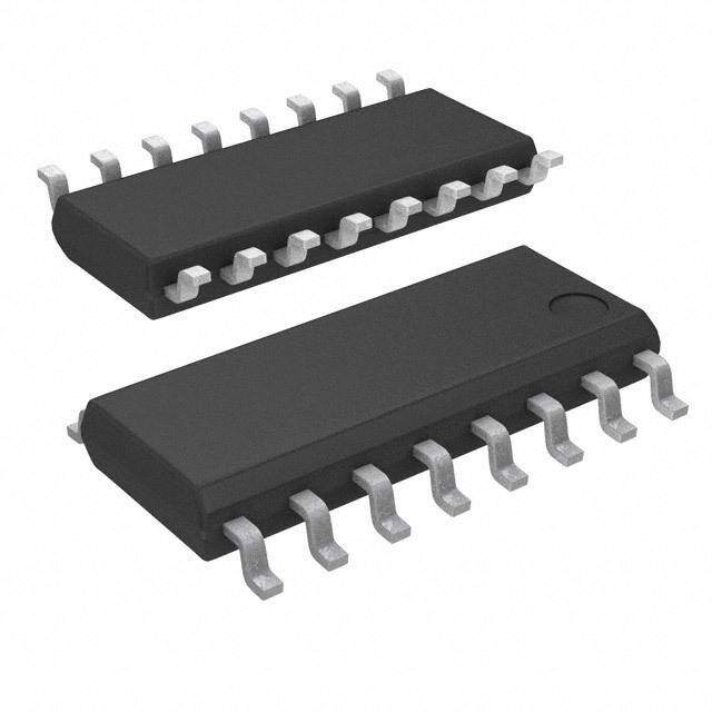
| 描述 | IC OPAMP GP 3MHZ RRO 16SOIC运算放大器 - 运放 Quad 3MHz R/R |
| 产品分类 | Linear - Amplifiers - Instrumentation, OP Amps, Buffer Amps集成电路 - IC |
| 品牌 | Texas Instruments |
| 产品手册 | |
| 产品图片 |
|
| rohs | 符合RoHS无铅 / 符合限制有害物质指令(RoHS)规范要求 |
| 产品系列 | 放大器 IC,运算放大器 - 运放,Texas Instruments TLV2375IDR- |
| 数据手册 | |
| 产品型号 | TLV2375IDR |
| 产品种类 | 运算放大器 - 运放 |
| 供应商器件封装 | 16-SOIC N |
| 共模抑制比—最小值 | 67 dB |
| 关闭 | Shutdown |
| 其它名称 | 296-11969-6 |
| 包装 | Digi-Reel® |
| 单位重量 | 141.700 mg |
| 压摆率 | 2.1 V/µs |
| 双重电源电压 | +/- 3 V, +/- 5 V |
| 商标 | Texas Instruments |
| 增益带宽生成 | 3 MHz |
| 增益带宽积 | 3MHz |
| 安装类型 | 表面贴装 |
| 安装风格 | SMD/SMT |
| 封装 | Reel |
| 封装/外壳 | 16-SOIC(0.154",3.90mm 宽) |
| 封装/箱体 | SOIC-16 |
| 工作温度 | -40°C ~ 125°C |
| 工作电源电压 | 2.7 V to 16 V, +/- 1.35 V to +/- 8 V |
| 工厂包装数量 | 2500 |
| 放大器类型 | 通用 |
| 最大双重电源电压 | +/- 8 V |
| 最大工作温度 | + 125 C |
| 最小双重电源电压 | +/- 1.35 V |
| 最小工作温度 | - 40 C |
| 标准包装 | 1 |
| 电压-电源,单/双 (±) | 2.7 V ~ 16 V, ±1.35 V ~ 8 V |
| 电压-输入失调 | 2mV |
| 电流-电源 | 750µA |
| 电流-输入偏置 | 1pA |
| 电流-输出/通道 | 16mA |
| 电源电流 | 3.6 mA |
| 电路数 | 4 |
| 系列 | TLV2375 |
| 转换速度 | 2.4 V/us |
| 输入偏压电流—最大 | 60 pA |
| 输入参考电压噪声 | 39 nV |
| 输入补偿电压 | 4.5 mV |
| 输出电流 | 16 mA |
| 输出类型 | 满摆幅 |
| 通道数量 | 4 Channel |


- 商务部:美国ITC正式对集成电路等产品启动337调查
- 曝三星4nm工艺存在良率问题 高通将骁龙8 Gen1或转产台积电
- 太阳诱电将投资9.5亿元在常州建新厂生产MLCC 预计2023年完工
- 英特尔发布欧洲新工厂建设计划 深化IDM 2.0 战略
- 台积电先进制程称霸业界 有大客户加持明年业绩稳了
- 达到5530亿美元!SIA预计今年全球半导体销售额将创下新高
- 英特尔拟将自动驾驶子公司Mobileye上市 估值或超500亿美元
- 三星加码芯片和SET,合并消费电子和移动部门,撤换高东真等 CEO
- 三星电子宣布重大人事变动 还合并消费电子和移动部门
- 海关总署:前11个月进口集成电路产品价值2.52万亿元 增长14.8%


PDF Datasheet 数据手册内容提取
Product Sample & Technical Tools & Support & Reference Folder Buy Documents Software Community Design TLV2370,TLV2371,TLV2372 TLV2373,TLV2374,TLV2375 SLOS270F–MARCH2001–REVISEDAUGUST2016 TLV237x 500-µA/Ch, 3-MHz Rail-to-Rail Input and Output Operational Amplifiers With Shutdown 1 Features 3 Description • Rail-to-RailInputandOutput The TLV237x single-supply operational amplifiers 1 provide rail-to-rail input and output capability. The • WideBandwidth:3MHz TLV237x takes the minimum operating supply voltage • HighSlewRate:2.4V/μs down to 2.7 V over the extended industrial • SupplyVoltageRange:2.7Vto16V temperature range while adding the rail-to-rail output swing feature. The TLV237x also provides 3-MHz • SupplyCurrent:550μA/Channel bandwidth from only 550 μA. The maximum • Low-PowerShutdownMode recommended supply voltage is 16 V, which allows – I :25 μA/Channel the devices to be operated from (±8-V supplies down DD(SHDN) to±1.35V)avarietyofrechargeablecells. • InputNoiseVoltage:39nV/√Hz • InputBiasCurrent:1pA The CMOS inputs enable use in high-impedance sensor interfaces, with the lower voltage operation • SpecifiedTemperatureRange: making an ideal alternative for the TLC227x in – −40°Cto+125°C(IndustrialGrade) battery-powered applications. The rail-to-rail input • Ultra-SmallPackaging: stage further increases its versatility. The TLV237x is the seventh member of a rapidly growing number of – 5-or6-PinSOT-23(TLV2370,TLV2371) RRIO products available from TI, and it is the first to – 8-or10-PinMSOP(TLV2372,TLV2373) allow operation up to 16-V rails with good ac performance. 2 Applications All members are available in PDIP and SOIC with the • WhiteGoods singles in the small SOT-23 package, duals in the • HandheldTestEquipment MSOP,andquadsintheTSSOPpackage. • PortableBloodGlucoseSystems The 2.7-V operation makes the TLV237x compatible • RemoteSensing withLi-Ionpoweredsystemsandtheoperatingsupply voltage range of many micro-power microcontrollers • ActiveFilters availabletodayincludingTI’sMSP430. • IndustrialAutomation • Battery-PoweredElectronics DeviceInformation(1) PARTNUMBER PACKAGE BODYSIZE(NOM) OperationalAmplifier PDIP(8) 9.81mm×6.35mm PDIP(14) 19.30mm×6.35mm − SOIC(8) 4.90mm×3.91mm + SOIC(14) 8.65mm×3.91mm TSSOP(14) TLV237x 5.00mm×4.40mm TSSOP(16) SOT-23(6) 2.90mm×1.60mm SOT-23(5) VSSOP(8) 3.00mm×3.00mm VSSOP(10) (1) For all available packages, see the orderable addendum at theendofthedatasheet. 1 An IMPORTANT NOTICE at the end of this data sheet addresses availability, warranty, changes, use in safety-critical applications, intellectualpropertymattersandotherimportantdisclaimers.PRODUCTIONDATA.
TLV2370,TLV2371,TLV2372 TLV2373,TLV2374,TLV2375 SLOS270F–MARCH2001–REVISEDAUGUST2016 www.ti.com Table of Contents 1 Features.................................................................. 1 8.3 FeatureDescription.................................................22 2 Applications........................................................... 1 8.4 DeviceFunctionalModes........................................24 3 Description............................................................. 1 9 ApplicationandImplementation........................ 25 4 RevisionHistory..................................................... 2 9.1 ApplicationInformation............................................25 9.2 TypicalApplication..................................................25 5 DeviceComparisonTables................................... 3 10 PowerSupplyRecommendations..................... 27 6 PinConfigurationandFunctions......................... 3 11 Layout................................................................... 27 7 Specifications......................................................... 8 11.1 LayoutGuidelines.................................................27 7.1 AbsoluteMaximumRatings......................................8 11.2 LayoutExample....................................................27 7.2 RecommendedOperatingConditions.......................8 11.3 PowerDissipationConsiderations........................28 7.3 ThermalInformation:TLV2370.................................9 12 DeviceandDocumentationSupport................. 29 7.4 ThermalInformation:TLV2371.................................9 7.5 ThermalInformation:TLV2372.................................9 12.1 DocumentationSupport........................................29 7.6 ThermalInformation:TLV2373...............................10 12.2 RelatedLinks........................................................29 7.7 ThermalInformation:TLV2374...............................10 12.3 ReceivingNotificationofDocumentationUpdates29 7.8 ThermalInformation:TLV2375...............................10 12.4 CommunityResources..........................................29 7.9 ElectricalCharacteristics.........................................11 12.5 Trademarks...........................................................29 7.10 TypicalCharacteristics..........................................15 12.6 ElectrostaticDischargeCaution............................29 12.7 Glossary................................................................29 8 DetailedDescription............................................ 22 13 Mechanical,Packaging,andOrderable 8.1 Overview.................................................................22 Information........................................................... 30 8.2 FunctionalBlockDiagram.......................................22 4 Revision History ChangesfromRevisionE(May2016)toRevisionF Page • Changednamesofpins2and3inTLV2372D,DGK,andPpackagespinoutdiagram...................................................... 4 ChangesfromRevisionD(January2005)toRevisionE Page • AddedESDRatingstable,FeatureDescriptionsection,DeviceFunctionalModes,ApplicationandImplementation section,PowerSupplyRecommendationssection,Layoutsection,DeviceandDocumentationSupportsection,and Mechanical,Packaging,andOrderableInformationsection.................................................................................................. 1 • DeletedTLV2370andTLV2371AvailableOptions,TLV2372ANDTLV2373AvailableOptions,andTLV2374and TLV2375AvailableOptionstables......................................................................................................................................... 3 • DeletedContinuoustotalpowerdissipationandleadtemperaturespecificationsfromAbsoluteMaximumRatingstable...8 • DeletedDissipationRatingstable........................................................................................................................................ 14 2 SubmitDocumentationFeedback Copyright©2001–2016,TexasInstrumentsIncorporated ProductFolderLinks:TLV2370 TLV2371 TLV2372TLV2373 TLV2374 TLV2375
TLV2370,TLV2371,TLV2372 TLV2373,TLV2374,TLV2375 www.ti.com SLOS270F–MARCH2001–REVISEDAUGUST2016 5 Device Comparison Tables Table1.SelectionofSignalAmplifierProducts(1) SINGLES, V V I /Ch I GBW SR RAIL-TO- DEVICE DD IO Q IB SHUTDOWN DUALS, (V) (µV) (µA) (pA) (MHz) (V/µs) RAIL QUADS TLV237x 2.7to16 500 550 1 3 2.4 Yes I/O S,D,Q TLC227x 4to16 300 1100 1 2.2 3.6 — O D,Q TLV27x 2.7to16 500 550 1 3 2.4 — O S,D,Q TLC27x 3to16 1100 675 1 1.7 3.6 — — S,D,Q TLV246x 2.7to16 150 550 1300 6.4 1.6 Yes I/O S,D,Q TLV247x 2.7to16 250 600 2 2.8 1.5 Yes I/O S,D,Q TLV244x 2.7to10 300 725 1 1.8 1.4 — O D,Q (1) Typicalvaluesmeasuredat5Vand25°C. Table2.FamilyPackageTable(1) PACKAGETYPES UNIVERSAL NUMBEROF DEVICE SHUTDOWN EVM CHANNELS PDIP SOIC SOT-23 TSSOP MSOP BOARD TLV2370 1 8 8 6 — — Yes TLV2371 1 8 8 5 — — — TLV2372 2 8 8 — — 8 — SeetheEVM Selection TLV2373 2 14 14 — — 10 Yes Guide TLV2374 4 14 14 — 14 — — TLV2375 4 16 16 — 16 — Yes (1) Forthemostcurrentpackageandorderinginformation,seethePackageOptionAddendumattheendofthisdocument,orseetheTI websiteatwww.ti.com. 6 Pin Configuration and Functions TLV2370DBVPackage 6-PinSOT-23 TLV2370DandPPackages TopView 8-PinSOICandPDIP TopView OUT 1 6 V DD NC 1 8 SHDN GND 2 5 SHDN IN- 2 7 VDD IN+ 3 6 OUT IN+ 3 4 IN- GND 4 5 NC PinFunctions:TLV2370 PIN I/O DESCRIPTION NAME SOT-23 SOIC,PDIP GND 2 4 — Groundconnection IN– 4 2 I Negative(inverting)input IN+ 3 3 I Positive(noninverting)input NC — 1,5 — Nointernalconnection(canbeleftfloating) OUT 1 6 O Output SHDN 5 8 I Shutdowncontrol(activelow,canbeleftfloating) V 6 7 — Positivepowersupply DD Copyright©2001–2016,TexasInstrumentsIncorporated SubmitDocumentationFeedback 3 ProductFolderLinks:TLV2370 TLV2371 TLV2372TLV2373 TLV2374 TLV2375
TLV2370,TLV2371,TLV2372 TLV2373,TLV2374,TLV2375 SLOS270F–MARCH2001–REVISEDAUGUST2016 www.ti.com TLV2371DBVPackage TLV2371DandPPackages 5-PinSOT-23 8-PinSOICandPDIP TopView TopView OUT 1 5 VDD NC 1 8 NC IN- 2 7 V DD GND 2 IN+ 3 6 OUT GND 4 5 NC IN+ 3 4 IN- PinFunctions:TLV2371 PIN I/O DESCRIPTION NAME SOT-23 SOIC,PDIP GND 2 4 — Groundconnection IN– 4 2 I Negative(inverting)input IN+ 3 3 I Positive(noninverting)input NC — 1,5,8 — Nointernalconnection(canbeleftfloating) OUT 1 6 O Output V 5 7 — Positivepowersupply DD TLV2372D,DGK,andPPackages 8-PinSOIC,VSSOP,andPDIP TopView 1OUT 1 8 VDD 1IN- 2 7 2OUT 1IN+ 3 6 2IN- GND 4 5 2IN+ PinFunctions:TLV2372 PIN SOIC,VSSOP, I/O DESCRIPTION NAME PDIP GND 4 — Groundconnection 1IN– 2 I Invertinginput,channel1 1IN+ 3 I Noninvertinginput,channel1 2IN– 6 I Invertinginput,channel2 2IN+ 5 I Noninvertinginput,channel2 1OUT 1 O Output,channel1 2OUT 7 O Output,channel2 V 8 — Positivepowersupply DD 4 SubmitDocumentationFeedback Copyright©2001–2016,TexasInstrumentsIncorporated ProductFolderLinks:TLV2370 TLV2371 TLV2372TLV2373 TLV2374 TLV2375
TLV2370,TLV2371,TLV2372 TLV2373,TLV2374,TLV2375 www.ti.com SLOS270F–MARCH2001–REVISEDAUGUST2016 TLV2373DGSPackage TLV2373DandNPackages 10-PinVSSOP 14-PinSOICandPDIP TopView TopView 1OUT 1 10 VDD 1OUT 1 14 VDD 1IN- 2 9 2OUT 1IN- 2 13 2OUT 1IN+ 3 8 2IN- 1IN+ 3 12 2IN- GND 4 7 2IN+ GND 4 11 2IN+ 1SHDN 5 6 2SHDN NC 5 10 NC 1SHDN 6 9 2SHDN NC 7 8 NC PinFunctions:TLV2373 PIN I/O DESCRIPTION NAME SOIC,PDIP VSSOP GND 4 4 — Groundconnection 1IN– 2 2 I Invertinginput,channel1 1IN+ 3 3 I Noninvertinginput,channel1 2IN– 12 8 I Invertinginput,channel2 2IN+ 11 7 I Noninvertinginput,channel2 1OUT 1 1 O Output,channel1 2OUT 13 9 O Output,channel2 1SHDN 6 5 I Shutdowncontrol,channel1,(activelow,canbeleftfloating) 2SHDN 9 6 I Shutdowncontrol,channel2,(activelow,canbeleftfloating) V 14 10 — Positivepowersupply DD NC 5,7,8,10 — — Nointernalconnection(canbeleftfloating) Copyright©2001–2016,TexasInstrumentsIncorporated SubmitDocumentationFeedback 5 ProductFolderLinks:TLV2370 TLV2371 TLV2372TLV2373 TLV2374 TLV2375
TLV2370,TLV2371,TLV2372 TLV2373,TLV2374,TLV2375 SLOS270F–MARCH2001–REVISEDAUGUST2016 www.ti.com TLV2374D,N,andPWPackages 14-PinSOIC,PDIP,andTSSOP TopView 1OUT 1 14 4OUT 1IN- 2 13 4IN- 1IN+ 3 12 4IN+ V 4 11 GND DD 2IN+ 5 10 3IN+ 2IN- 6 9 3IN- 2OUT 7 8 3OUT PinFunctions:TLV2374 PIN I/O DESCRIPTION NAME SOIC,PDIP,TSSOP GND 11 — Groundconnection 1IN– 2 I Invertinginput,channel1 1IN+ 3 I Noninvertinginput,channel1 2IN– 6 I Invertinginput,channel2 2IN+ 5 I Noninvertinginput,channel2 3IN– 9 I Invertinginput,channel3 3IN+ 10 I Noninvertinginput,channel3 4IN– 13 I Invertinginput,channel4 4IN+ 12 I Noninvertinginput,channel4 1OUT 1 O Output,channel1 2OUT 7 O Output,channel2 3OUT 8 O Output,channel3 4OUT 14 O Output,channel4 V 4 — Positivepowersupply DD 6 SubmitDocumentationFeedback Copyright©2001–2016,TexasInstrumentsIncorporated ProductFolderLinks:TLV2370 TLV2371 TLV2372TLV2373 TLV2374 TLV2375
TLV2370,TLV2371,TLV2372 TLV2373,TLV2374,TLV2375 www.ti.com SLOS270F–MARCH2001–REVISEDAUGUST2016 TLV2375D,N,andPWPackages 16-PinSOIC,PDIP,andTSSOP TopView 1OUT 1 16 4OUT 1IN− 2 15 4IN− 1IN+ 3 14 4IN+ VDD+ 4 13 GND 2IN+ 5 12 3IN+ 2IN− 6 11 3IN− 2OUT 7 10 3OUT 1/2SHDN 8 9 3/4SHDN PinFunctions:TLV2375 PIN I/O DESCRIPTION NAME SOIC,PDIP,TSSOP GND 13 — Groundconnection 1IN– 2 I Invertinginput,channel1 2IN– 6 I Invertinginput,channel2 3IN– 11 I Invertinginput,channel3 4IN– 15 I Invertinginput,channel4 1IN+ 3 I Noninvertinginput,channel1 2IN+ 5 I Noninvertinginput,channel2 3IN+ 12 I Noninvertinginput,channel3 4IN+ 14 I Noninvertinginput,channel4 1OUT 1 O Output,channel1 2OUT 7 O Output,channel2 3OUT 10 O Output,channel3 4OUT 16 O Output,channel4 1/2SHDN 8 I Shutdowncontrol,channels1and2,(activelow,canbeleftfloating) 3/4SHDN 9 I Shutdowncontrol,channels3and4,(activelow,canbeleftfloating) V 4 — Positivepowersupply DD TYPICALPIN1INDICATORS Pin 1 Printedor Pin 1 Pin 1 Pin 1 Molded Dot Stripe Bevel Edges Molded“U”Shape IfthereisnotaPin1indicator,turndevicetoenablereadingthesymbolfromthelefttoright.Pin1isatthelowerleft cornerofthedevice. Figure1. TypicalPin1Indicators Copyright©2001–2016,TexasInstrumentsIncorporated SubmitDocumentationFeedback 7 ProductFolderLinks:TLV2370 TLV2371 TLV2372TLV2373 TLV2374 TLV2375
TLV2370,TLV2371,TLV2372 TLV2373,TLV2374,TLV2375 SLOS270F–MARCH2001–REVISEDAUGUST2016 www.ti.com 7 Specifications 7.1 Absolute Maximum Ratings overoperatingfree-airtemperaturerange(unlessotherwisenoted)(1) MIN MAX UNIT Supplyvoltage,V (2) 16.5 DD Voltage Differentialinputvoltage,V –V V V ID DD DD Inputvoltage,V(2) –0.2 V +0.2 I DD Inputcurrent,I –10 10 IN Current mA Outputcurrent,I –100 100 O Operatingfree-airtemperature,T :I-suffix –40 125 A Temperature Maximumjunctiontemperature,T 150 °C J Storagetemperature,T –65 150 stg (1) StressesbeyondthoselistedunderAbsoluteMaximumRatingsmaycausepermanentdamagetothedevice.Thesearestressratings only,whichdonotimplyfunctionaloperationofthedeviceattheseoranyotherconditionsbeyondthoseindicatedunderRecommended OperatingConditions.Exposuretoabsolute-maximum-ratedconditionsforextendedperiodsmayaffectdevicereliability. (2) Allvoltagevalues,exceptdifferentialvoltages,arewithrespecttoGND. 7.2 Recommended Operating Conditions overoperatingfree-airtemperaturerange(unlessotherwisenoted). MIN MAX UNIT Singlesupply 2.7 16 Supplyvoltage,V V DD Splitsupply ±1.35 ±8 Common-modeinputvoltage,V 0 V V CM DD Operatingfree-airtemperature,T I-suffix –40 125 °C A Turnonvoltage(shutdownpinvoltagelevel),V ,relativetoGNDpinvoltage 2 V (ON) Turnoff(shutdownpinvoltagelevel),V ,relativetoGNDpinvoltage 0.8 V (OFF) 8 SubmitDocumentationFeedback Copyright©2001–2016,TexasInstrumentsIncorporated ProductFolderLinks:TLV2370 TLV2371 TLV2372TLV2373 TLV2374 TLV2375
TLV2370,TLV2371,TLV2372 TLV2373,TLV2374,TLV2375 www.ti.com SLOS270F–MARCH2001–REVISEDAUGUST2016 7.3 Thermal Information: TLV2370 TLV2370 THERMALMETRIC(1) DBV(SOT-23) D(SOIC) P(PDIP) UNIT 6PINS 8PINS 8PINS R Junction-to-ambientthermalresistance 228.5 138.4 49.2 °C/W θJA R Junction-to-case(top)thermalresistance 99.1 89.5 39.4 °C/W θJC(top) R Junction-to-boardthermalresistance 54.6 78.6 26.4 °C/W θJB ψ Junction-to-topcharacterizationparameter 7.7 29.9 15.4 °C/W JT ψ Junction-to-boardcharacterizationparameter 53.8 78.1 26.3 °C/W JB R Junction-to-case(bottom)thermalresistance n/a n/a n/a °C/W θJC(bot) (1) Formoreinformationabouttraditionalandnewthermalmetrics,seetheSemiconductorandICPackageThermalMetricsapplication report. 7.4 Thermal Information: TLV2371 TLV2371 THERMALMETRIC(1) DBV(SOT-23) D(SOIC) P(PDIP) UNIT 5PINS 8PINS 8PINS R Junction-to-ambientthermalresistance 228.5 138.4 49.2 °C/W θJA R Junction-to-case(top)thermalresistance 99.1 89.5 39.4 °C/W θJC(top) R Junction-to-boardthermalresistance 54.6 78.6 26.4 °C/W θJB ψ Junction-to-topcharacterizationparameter 7.7 29.9 15.4 °C/W JT ψ Junction-to-boardcharacterizationparameter 53.8 78.1 26.3 °C/W JB R Junction-to-case(bottom)thermalresistance n/a n/a n/a °C/W θJC(bot) (1) Formoreinformationabouttraditionalandnewthermalmetrics,seetheSemiconductorandICPackageThermalMetricsapplication report. 7.5 Thermal Information: TLV2372 TLV2372 THERMALMETRIC(1) D(SOIC) DGK(VSSOP) P(PDIP) UNIT 8PINS 8PINS 8PINS R Junction-to-ambientthermalresistance 138.4 191.2 49.2 °C/W θJA R Junction-to-case(top)thermalresistance 89.5 61.9 39.4 °C/W θJC(top) R Junction-to-boardthermalresistance 78.6 111.9 26.4 °C/W θJB ψ Junction-to-topcharacterizationparameter 29.9 5.1 15.4 °C/W JT ψ Junction-to-boardcharacterizationparameter 78.1 110.2 26.3 °C/W JB R Junction-to-case(bottom)thermalresistance n/a n/a n/a °C/W θJC(bot) (1) Formoreinformationabouttraditionalandnewthermalmetrics,seetheSemiconductorandICPackageThermalMetricsapplication report. Copyright©2001–2016,TexasInstrumentsIncorporated SubmitDocumentationFeedback 9 ProductFolderLinks:TLV2370 TLV2371 TLV2372TLV2373 TLV2374 TLV2375
TLV2370,TLV2371,TLV2372 TLV2373,TLV2374,TLV2375 SLOS270F–MARCH2001–REVISEDAUGUST2016 www.ti.com 7.6 Thermal Information: TLV2373 TLV2373 THERMALMETRIC(1) DGS(VSSOP) D(SOIC) P(PDIP) UNIT 10PINS 14PINS 14PINS R Junction-to-ambientthermalresistance 166.5 67 66.3 °C/W θJA R Junction-to-case(top)thermalresistance 41.8 24.1 20.5 °C/W θJC(top) R Junction-to-boardthermalresistance 86.1 22.5 26.8 °C/W θJB ψ Junction-to-topcharacterizationparameter 1.5 2.2 2.1 °C/W JT ψ Junction-to-boardcharacterizationparameter 84.7 22.1 26.2 °C/W JB R Junction-to-case(bottom)thermalresistance n/a n/a n/a °C/W θJC(bot) (1) Formoreinformationabouttraditionalandnewthermalmetrics,seetheSemiconductorandICPackageThermalMetricsapplication report. 7.7 Thermal Information: TLV2374 TLV2374 THERMALMETRIC(1) D(SOIC) N(PDIP) PW(TSSOP) UNIT 14PINS 14PINS 14PINS R Junction-to-ambientthermalresistance 67 66.3 121 °C/W θJA R Junction-to-case(top)thermalresistance 24.1 20.5 49.4 °C/W θJC(top) R Junction-to-boardthermalresistance 22.5 26.8 62.8 °C/W θJB ψ Junction-to-topcharacterizationparameter 2.2 2.1 5.9 °C/W JT ψ Junction-to-boardcharacterizationparameter 22.1 26.2 62.2 °C/W JB R Junction-to-case(bottom)thermalresistance n/a n/a n/a °C/W θJC(bot) (1) Formoreinformationabouttraditionalandnewthermalmetrics,seetheSemiconductorandICPackageThermalMetricsapplication report. 7.8 Thermal Information: TLV2375 TLV2375 THERMALMETRIC(1) D(SOIC) N(PDIP) PW(TSSOP) UNIT 16PINS 16PINS 16PINS R Junction-to-ambientthermalresistance 83 55.8 115.6 °C/W θJA R Junction-to-case(top)thermalresistance 44 43.1 50.5 °C/W θJC(top) R Junction-to-boardthermalresistance 40.5 35.8 60.7 °C/W θJB ψ Junction-to-topcharacterizationparameter 11.5 27.9 7.4 °C/W JT ψ Junction-to-boardcharacterizationparameter 40.2 35.7 60.1 °C/W JB R Junction-to-case(bottom)thermalresistance n/a n/a n/a °C/W θJC(bot) (1) Formoreinformationabouttraditionalandnewthermalmetrics,seetheSemiconductorandICPackageThermalMetricsapplication report. 10 SubmitDocumentationFeedback Copyright©2001–2016,TexasInstrumentsIncorporated ProductFolderLinks:TLV2370 TLV2371 TLV2372TLV2373 TLV2374 TLV2375
TLV2370,TLV2371,TLV2372 TLV2373,TLV2374,TLV2375 www.ti.com SLOS270F–MARCH2001–REVISEDAUGUST2016 7.9 Electrical Characteristics atT =25°C,V =2.7V,5V,and15V(unlessotherwisenoted). A DD PARAMETER TESTCONDITIONS MIN TYP MAX UNIT DCPERFORMANCE AtT =25°C,V =V /2,V =V /2,R =50Ω 2 4.5 mV A IC DD O DD S VOS Inputoffsetvoltage AtTA=–40°Cto+125°C,VIC=VDD/2,VO=VDD/2, 6 mV R =50Ω S dV /dT Offsetvoltagedrift AtT =25°C,V =V /2,V =V /2,R =50Ω 2 µV/°C OS A IC DD O DD S V =0toV 50 68 IC DD AtT =–40°Cto+125°C, A 49 VDD=2.7V, VIC=0toVDD RS=50Ω VIC=0toVDD−1.35V 56 70 AtT =–40°Cto+125°C, A 54 V =0toV −1.35V IC DD V =0toV 55 72 IC DD AtT =–40°Cto+125°C, A 54 CMRR Common-moderejectionratio VDD=5V, VIC=0toVDD dB RS=50Ω VIC=0toVDD−1.35V 67 80 AtT =–40°Cto+125°C, A 64 V =0toV −1.35V IC DD V =0toV 64 82 IC DD AtT =–40°Cto+125°C, A 63 VDD=15V, VIC=0toVDD RS=50Ω VIC=0toVDD−1.35V 67 84 AtT =–40°Cto+125°C, A 66 V =0toV −1.35V IC DD V =2.7V, 98 106 DD V = O(PP) VDD/2, AtTA=–40°Cto+125°C 76 R =10kΩ L V =5V, 100 110 DD Large-signaldifferential V = A O(PP) dB VD voltageamplification VDD/2, AtTA=–40°Cto+125°C 86 R =10kΩ L V =15V, 81 83 DD V = O(PP) VDD/2, AtTA=–40°Cto+125°C 79 R =10kΩ L INPUTCHARACTERISTICS 1 60 V =15V, DD I Inputoffsetcurrent V =V = AtT =70°C 100 pA OS IC O A V /2 DD AtT =125°C 1000 A 1 60 V =15V, DD I Inputbiascurrent V =V = AtT =70°C 100 pA B IC O A V /2 DD AtT =125°C 1000 A Differentialinputresistance 1000 GΩ Common-modeinput f=21kHz 8 pF capacitance Copyright©2001–2016,TexasInstrumentsIncorporated SubmitDocumentationFeedback 11 ProductFolderLinks:TLV2370 TLV2371 TLV2372TLV2373 TLV2374 TLV2375
TLV2370,TLV2371,TLV2372 TLV2373,TLV2374,TLV2375 SLOS270F–MARCH2001–REVISEDAUGUST2016 www.ti.com Electrical Characteristics (continued) atT =25°C,V =2.7V,5V,and15V(unlessotherwisenoted). A DD PARAMETER TESTCONDITIONS MIN TYP MAX UNIT OUTPUTCHARACTERISTICS AtT =25°C,V =V /2,I =−1mA 2.55 2.58 A IC DD OH VDD=2.7V AtTA=–40°Cto+125°C,VIC=VDD/2, 2.48 I =−1mA OH AtT =25°C,V =V /2,I =−1mA 4.9 4.93 A IC DD OH VDD=5V AtTA=–40°Cto+125°C,VIC=VDD/2, 4.85 I =−1mA OH AtT =25°C,V =V /2,I =−1mA 14.92 14.96 A IC DD OH VDD=15V AtTA=–40°Cto+125°C,VIC=VDD/2, 14.9 I =−1mA OH V High-leveloutputvoltage OH AtT =25°C,V =V /2,I =−5mA 1.9 2 V A IC DD OH VDD=2.7V AtTA=–40°Cto+125°C,VIC=VDD/2, 1.6 I =−5mA OH AtT =25°C,V =V /2,I =−5mA 4.6 4.68 A IC DD OH VDD=5V AtTA=–40°Cto+125°C,VIC=VDD/2, 4.5 I =−5mA OH AtT =25°C,V =V /2,I =−5mA 14.7 14.8 A IC DD OH VDD=15V AtTA=–40°Cto+125°C,VIC=VDD/2, 14.6 I =−5mA OH AtT =25°C,V =V /2,I =1mA 0.1 0.15 A IC DD OL VDD=2.7V AtTA=–40°Cto+125°C,VIC=VDD/2, 0.22 I =1mA OL AtT =25°C,V =V /2,I =1mA 0.05 0.1 A IC DD OL VDD=5V AtTA=–40°Cto+125°C,VIC=VDD/2, 0.15 I =1mA OL AtT =25°C,V =V /2,I =1mA 0.05 0.08 A IC DD OL VDD=15V AtTA=–40°Cto+125°C,VIC=VDD/2, 0.1 I =1mA OL V Low-leveloutputvoltage OL AtT =25°C,V =V /2,I =5mA 0.52 0.7 V A IC DD OL VDD=2.7V AtTA=–40°Cto+125°C,VIC=VDD/2, 1.1 I =5mA OL AtT =25°C,V =V /2,I =5mA 0.28 0.4 A IC DD OL VDD=5V AtTA=–40°Cto+125°C,VIC=VDD/2, 0.5 I =5mA OL AtT =25°C,V =V /2,I =5mA 0.19 0.3 A IC DD OL VDD=15V AtTA=–40°Cto+125°C,VIC=VDD/2, 0.35 I =5mA OL V =2.7V, Positiverail 4 DD V =0.5V O fromrail Negativerail 5 V =5V, Positiverail 7 DD I Outputcurrent V =0.5V mA O O fromrail Negativerail 8 V =15V, Positiverail 16 DD V =0.5V O fromrail Negativerail 15 12 SubmitDocumentationFeedback Copyright©2001–2016,TexasInstrumentsIncorporated ProductFolderLinks:TLV2370 TLV2371 TLV2372TLV2373 TLV2374 TLV2375
TLV2370,TLV2371,TLV2372 TLV2373,TLV2374,TLV2375 www.ti.com SLOS270F–MARCH2001–REVISEDAUGUST2016 Electrical Characteristics (continued) atT =25°C,V =2.7V,5V,and15V(unlessotherwisenoted). A DD PARAMETER TESTCONDITIONS MIN TYP MAX UNIT POWERSUPPLY V =2.7V,V =V /2 470 560 DD O DD V =5V,V =V /2 550 660 DD O DD I Supplycurrent(perchannel) µA DD VDD=15V, AtTA=25°C 750 900 VO=VDD/2 AtTA=–40°Cto+125°C 1200 V =2.7V AtT =25°C 70 80 DD A Power-supplyrejectionratio to15V, PSRR dB (ΔVDD/ΔVIO) VIC=VDD/2, AtTA=–40°Cto+125°C 65 noload DYNAMICPERFORMANCE V =2.7V R =2kΩ,C =10pF 2.4 DD L L UGBW Unitygainbandwidth V =5Vto MHz DD R =2kΩ,C =10pF 3 15V L L AtT =25°C,V =V /2, A O(PP) DD 1.4 2 C =50pF,R =10kΩ L L VDD=2.7V AtTA=–40°Cto+125°C,VO(PP)= V /2, 1 DD C =50pF,R =10kΩ L L AtT =25°C,V =V /2, A O(PP) DD 1.6 2.4 C =50pF,R =10kΩ L L SR Slewrateatunitygain VDD=5V AtTA=–40°Cto+125°C,VO(PP)= V/µs V /2, 1.2 DD C =50pF,R =10kΩ L L AtT =25°C,V =V /2, A O(PP) DD 1.9 2.1 C =50pF,R =10kΩ L L VDD=15V AtTA=–40°Cto+125°C,VO(PP)= V /2, 1.4 DD C =50pF,R =10kΩ L L φm Phasemargin R =2kΩ,C =100pF 65 ° L L Gainmargin R =2kΩ,C =10pF 18 dB L L V =2.7V,V =1V,A =−1, DD (STEP)PP V 2.9 C =10pF,R =2kΩ,0.1% L L t Settlingtime µs s V =5V,15V,V =1V,A =−1, DD (STEP)PP V 2 C =47pF,R =2kΩ,0.1% L L Copyright©2001–2016,TexasInstrumentsIncorporated SubmitDocumentationFeedback 13 ProductFolderLinks:TLV2370 TLV2371 TLV2372TLV2373 TLV2374 TLV2375
TLV2370,TLV2371,TLV2372 TLV2373,TLV2374,TLV2375 SLOS270F–MARCH2001–REVISEDAUGUST2016 www.ti.com Electrical Characteristics (continued) atT =25°C,V =2.7V,5V,and15V(unlessotherwisenoted). A DD PARAMETER TESTCONDITIONS MIN TYP MAX UNIT NOISE,DISTORTIONPERFORMANCE V =V /2V,R =2kΩ, O(PP) DD L 0.02% f=10kHz,A =1 V V =V /2V,R =2kΩ, V =2.7V O(PP) DD L 0.05% DD f=10kHz,A =10 V V =V /2V,R =2kΩ, O(PP) DD L 0.18% Totalharmonicdistortionplus f=10kHz,AV=100 THD+N noise V =V /2V,R =2kΩ, O(PP) DD L 0.02% f=10kHz,A =1 V V =5V, V =V /2V,R =2kΩ, DD O(PP) DD L 0.09% 15V f=10kHz,A =10 V V =V /2V,R =2kΩ, O(PP) DD L 0.5% f=10kHz,A =100 V Equivalentinputnoise f=1kHz 39 V nV/√Hz n voltage f=10kHz 35 I Equivalentinputnoisecurrent f=1kHz 0.6 fA/√Hz n SHUTDOWNCHARACTERISTICS V =2.7V, AtT =25°C 25 30 DD A 5V, Supplycurrentinshutdown SHDN=0V AtTA=–40°Cto+125°C 35 I mode(TLV2370,TLV2373, µA DD(SHDN) TLV2375)(perchannel) VDD=15V, AtTA=25°C 40 45 SHDN=0V AtT =–40°Cto+125°C 50 A t Amplifierturnontime(1) R =2kΩ 0.8 µs (on) L t Amplifierturnofftime(1) R =2kΩ 1 µs (off) L (1) DisabletimeandenabletimearedefinedastheintervalbetweenapplicationofthelogicsignaltotheSHDNterminalandthepointat whichthesupplycurrenthasreachedonehalfofitsfinalvalue. 14 SubmitDocumentationFeedback Copyright©2001–2016,TexasInstrumentsIncorporated ProductFolderLinks:TLV2370 TLV2371 TLV2372TLV2373 TLV2374 TLV2375
TLV2370,TLV2371,TLV2372 TLV2373,TLV2374,TLV2375 www.ti.com SLOS270F–MARCH2001–REVISEDAUGUST2016 7.10 Typical Characteristics Table3.TableofGraphs FIGURE V Inputoffsetvoltage vsCommon-modeinputvoltage Figure2,Figure3,Figure4 IO CMRR Common-moderejectionratio vsFrequency Figure5 Inputbiasandoffsetcurrent vsFree-airtemperature Figure6 V Low-leveloutputvoltage vsLow-leveloutputcurrent Figure7,Figure9,Figure11 OL V High-leveloutputvoltage vsHigh-leveloutputcurrent Figure8,Figure10,Figure12 OH V Peak-to-peakoutputvoltage vsFrequency Figure13 O(PP) I Supplycurrent vsSupplyvoltage Figure14 DD PSRR Powersupplyrejectionratio vsFrequency Figure15 A Differentialvoltagegainandphase vsFrequency Figure16 VD Gain-bandwidthproduct vsFree-airtemperature Figure17 vsSupplyvoltage Figure18 SR Slewrate vsFree-airtemperature Figure19 φm Phasemargin vsCapacitiveload Figure20 V Equivalentinputnoisevoltage vsFrequency Figure21 n Voltage-followerlarge-signalpulse Figure22,Figure23 response Voltage-followersmall-signalpulse Figure24 response Invertinglarge-signalresponse Figure25,Figure26 Invertingsmall-signalresponse Figure27 Crosstalk vsFrequency Figure28 Shutdownforward&reverseisolation vsFrequency Figure29 I Shutdownsupplycurrent vsSupplyvoltage Figure30 DD(SHDN) I Shutdownpinleakagecurrent vsShutdownpinvoltage Figure31 DD(SHDN) I Shutdownsupplycurrent,outputvoltage vsTime Figure32,Figure33 DD(SHDN) Copyright©2001–2016,TexasInstrumentsIncorporated SubmitDocumentationFeedback 15 ProductFolderLinks:TLV2370 TLV2371 TLV2372TLV2373 TLV2374 TLV2375
TLV2370,TLV2371,TLV2372 TLV2373,TLV2374,TLV2375 SLOS270F–MARCH2001–REVISEDAUGUST2016 www.ti.com 1000 1000 VDD= 2.7 V VDD= 5 V 800 TA= 25°C 800 TA= 25°C V) V) m m e ( 600 e ( 600 g g a a olt olt et V 400 et V 400 s s ut Off 200 ut Off 200 p p n n I 0 I 0 -200 -200 0 0.4 0.8 1.2 1.6 2 2.4 2.7 0 1 2 3 4 5 Common-Mode Input Voltage (V) Common-Mode Input Voltage (V) Figure2.InputOffsetVoltagevsCommon-ModeInput Figure3.InputOffsetVoltagevsCommon-ModeInput Voltage Voltage 1000 120 V = 15 V V)m 800 TADD= 25°C atio (dB) 100 VDD= 5 V, 15 V et Voltage ( 640000 Rejection R 8600 VDD= 2.7 V ut Offs 200 Mode 40 Inp 0 mmon- 20 o C -200 0 0 2 4 6 8 10 12 14 15 10 100 1 k 10 k 100 k 1 M Common-Mode Input Voltage (V) Frequency (Hz) Figure4.InputOffsetVoltagevsCommon-ModeInput Figure5.Common-ModeRejectionRatiovsFrequency Voltage 300 2.80 urrent (pA) 225000 VVDICD== V 2D.7D/ 2V, 5 V, 15 V Voltage (V) 2.402 VDD= 2.T7A V= 125°C Offset C 115000 Output 11..6200 TA= 70°C Bias/ 50 evel 0.80 TA= 25°C put w-L TA= 0°C In 0 Lo 0.40 T =-40°C A -50 0 -40 -25 -10 5 20 35 50 65 80 95 110 125 0 2 4 6 8 10 12 14 16 18 20 24 28 Temperature,TA(°C) Low-Level Output Current (mA) Figure6.InputBiasorOffsetCurrentvsFree-Air Figure7.Low-LevelOutputVoltagevsLow-LevelOutput Temperature Current 16 SubmitDocumentationFeedback Copyright©2001–2016,TexasInstrumentsIncorporated ProductFolderLinks:TLV2370 TLV2371 TLV2372TLV2373 TLV2374 TLV2375
TLV2370,TLV2371,TLV2372 TLV2373,TLV2374,TLV2375 www.ti.com SLOS270F–MARCH2001–REVISEDAUGUST2016 2.80 5 VDD= 2.7 V 4.50 VDD= 5 V age (V) 2.402 TA=-40°C age (V) 3.504 TTAA== 7 102°5C°C Volt TA= 125°C Volt 3 Output 11..6200 TA= 70°C Output 2.50 TA= 25°C TA= 0°C el T = 25°C el 2 High-Lev 00..8400 A TA= 0°C Low-Lev 1.501 TA=-40°C 0.50 0 0 0 1 2 3 4 5 6 7 8 9 10 11 12 0 5 10 15 20 25 30 35 40 45 50 55 60 65 70 High-Level Output Current (mA) Low-Level Output Current (mA) Figure8.High-LevelOutputVoltagevsHigh-LevelOutput Figure9.Low-LevelOutputVoltagevsLow-LevelOutput Current Current 5 15 e (V) 4.504 TA= 0°C VCC= 5 V e (V) 1142 VDD= 15 V TA= 125°C utput Voltag 32..55003 TA= 25°C TA=-40°C utput Voltag 180 TA= 70°C Level O 1.502 TA= 70°C Level O 64 TA= 25°C TA= 0°C High- 1 TA= 125°C Low- 2 TA=-40°C 0.50 0 0 0 5 10 15 20 25 30 35 40 45 0 20 40 60 80 100 120 140 160 High-Level Output Current (mA) Low-Level Output Current (mA) Figure10.High-LevelOutputVoltagevsHigh-LevelOutput Figure11.Low-LevelOutputVoltagevsLow-LevelOutput Current Current 15 16 High-Level Output Voltage (V) 1118604422 TATA= =2 57°T0C°AC=-40°C TAV=D D0°=C 15 V Peak-to-Peak Output Voltage (V) 11111154320198765432 VDD= 15 V VDDV=D D2.=7 5V V ARCTTAHVLLD==== 221-=5 01 k5° 0WpC%F T = 125°C 1 A 0 0 0 20 40 60 80 100 120 140 160 10 100 1 k 10 k 100 k 1 M 10 M High-Level Output Current (mA) Frequency (Hz) Figure12.High-LevelOutputVoltagevsHigh-LevelOutput Figure13.Peak-to-PeakOutputVoltagevsFrequency Current Copyright©2001–2016,TexasInstrumentsIncorporated SubmitDocumentationFeedback 17 ProductFolderLinks:TLV2370 TLV2371 TLV2372TLV2373 TLV2374 TLV2375
TLV2370,TLV2371,TLV2372 TLV2373,TLV2374,TLV2375 SLOS270F–MARCH2001–REVISEDAUGUST2016 www.ti.com 1 120 mA/Ch) 000...987 VAIVC== 2VDD/2 TA= 70°C TA= 125°C n Ratio (dB) 10800 VDD= 5 V, 15 V TA= 25°C Current ( 000...654 TA= 25°C y Rejectio 60 VDD= 2.7 V Supply 00..32 TA=-40°C TA= 0°C wer-Suppl 4200 0.1 Po 0 0 0 1 2 3 4 5 6 7 8 9 10 11 12 13 14 15 10 100 1 k 10 k 100 k 1 M Supply Voltage (V) Frequency (Hz) Figure14.SupplyCurrentvsSupplyVoltage Figure15.PowerSupplyRejectionRatiovsFrequency 120 180 4 V = 5 V DD ain (dB) 10800 Gain Phase 19305 ct (MHz) 3.53 VDD= 15 V ntial Voltage G 642000 V = 5 V 40-455 °Phae () ndwidth Produ 21..552 VDD= 2.7 V Differe -200 RCDLLD== 21 0k WpFDC --91035 Gain Ba 0.51 T = 25°C A -40 -180 0 10 100 1 k 10 k 100 k 1 M 10 M -40 -25 -10 5 20 35 50 65 80 95 110 125 Frequency (Hz) Temperature,T (°C) A Figure16.DifferentialVoltageGainandPhasevs Figure17.GainBandwidthProductvsFree-Air Frequency Temperature 3 3.5 SR- 2.5 3 SR- 2.5 s) 2 s) m m ate (V/ 1.5 SR+ ate (V/ 2 SR+ Slew R 1 AV= 1 Slew R 1.51 VADVD== 1 5 V R = 10 kW R = 10 kW 0.5 CL= 50 pF 0.5 CL= 50 pF L L TA= 25°C VI= 3 V 0 0 2.5 4.5 6.5 8.5 10.5 12.5 14.5 -40 -25 -10 5 20 35 50 65 80 95 110 125 Supply Voltage (V) Temperature,TA(°C) Figure18.SlewRatevsSupplyVoltage Figure19.SlewRatevsFree-AirTemperature 18 SubmitDocumentationFeedback Copyright©2001–2016,TexasInstrumentsIncorporated ProductFolderLinks:TLV2370 TLV2371 TLV2372TLV2373 TLV2374 TLV2375
TLV2370,TLV2371,TLV2372 TLV2373,TLV2374,TLV2375 www.ti.com SLOS270F–MARCH2001–REVISEDAUGUST2016 100 100 )z 90 ÖH 90 V/ 80 n 80 e ( °Margin () 765000 RNULL= 100 oise Voltag 765000 e N Phas 432000 VRDLD== 2 5k WV RNULL= 50 RNULL= 0 ent Input 432000 100 TAAV== 2O5p°eCn-Loop Equival 100 VTADD= =2 52°.7C V, 5 V, 15 V 10 100 1000 10 100 1 k 10 k 100 k Capacitive Load (pF) Frequency (Hz) Figure20.PhaseMarginvsCapacitiveLoad Figure21.EquivalentInputNoiseVoltagevsFrequency V) 4 V) 12 e ( 3 e ( 9 g g olta 2 VDD= 5 V olta 6 VDD= 15 V V A = 1 V A = 1 nput 10 VI RVL= 2 kW nput 30 VI RVL= 2 kW I CL= 10 pF I CL= 10 pF V = 3 V V = 9 V TI = 25°PCP 4 V) TI = 25°PCP 12 V) A 3 ge ( A 9 ge ( a a 2 olt 6 olt V V VO 10 utput VO 30 utput O O 0 2 4 6 8 10 12 14 16 18 0 2 4 6 8 10 12 14 16 18 Time (ms) Time (ms) Figure22.Voltage-FollowerLarge-SignalPulseResponse Figure23.Voltage-FollowerLarge-SignalPulseResponse V) V) Input Voltage (m 000...0018042 VI VARCDVLLD==== 211 05k WpVF Input Voltage ( 3210 VI VARCDVLLD==== 211 05k WpVF VO VTAI== 12050° CmVPP 0000...010428 Output Voltage (mV) VO VTAI== 32 5V°PCP 3210 Output Voltage (V) 0 0.2 0.4 0.6 0.8 1 1.2 1.4 1.6 1.8 0 2 4 6 8 10 12 14 16 Time (ms) Time (ms) Figure24.Voltage-FollowerSmall-SignalPulseResponse Figure25.InvertingLarge-SignalResponse Copyright©2001–2016,TexasInstrumentsIncorporated SubmitDocumentationFeedback 19 ProductFolderLinks:TLV2370 TLV2371 TLV2372TLV2373 TLV2374 TLV2375
TLV2370,TLV2371,TLV2372 TLV2373,TLV2374,TLV2375 SLOS270F–MARCH2001–REVISEDAUGUST2016 www.ti.com Input Voltage (V) 9630 VVARCTADIVLL=D==== = 9221- 5 011Vk° 5PWpC PFV VI VO 96 oltage (V) Input Voltage (V) 0.00.501 VI VO VVARCTADIVLL=D==== = 1221- 05 015k0° WpV CmFVPP 00..015 Voltage (V) 30 utput V 0 Output O 0 0.5 1 1.5 2 2.5 3 3.5 4 4.5 0 2 4 6 8 10 12 14 16 Time (ms) Time (ms) Figure27.InvertingSmall-SignalResponse Figure26.InvertingLarge-SignalResponse 0 V = 2.7 V, 5 V, 15 V dB) 160 -20 AVDI=D= V1DD/2 ation ( 140 VVDI=D =V D2D.7/2 V, 5 V, 15 V V ol R = 2 kW k (dB) --4600 RTAL== 225 k°WC everse Is 112000 ATCVLL=== 21150° pCF Crosstal -1-0800 Crosstalk in Shutdown ward and R 8600 A or 40 F -120 n w 20 Crosstalk o d -140 hut 0 S 10 100 1 k 10 k 100 k 10 100 1 k 10 k 100 k 1 M 10 M Frequency (Hz) Frequency (Hz) Figure28.CrosstalkvsFrequency Figure29.ShutdownForwardandReverseIsolationvs Frequency 50 250 y Current (A/Ch)m 4433250505 SVAHIV=D= V N1D=D /02 V TA= 70°C TA=T A1=25 2°5C°C akage Current (pA) 210500 TA= 125°C uppl 20 TA= 0°C n Le 100 Shutdown S 11505 TA=-40°C Shutdown Pi 50 0 0 0 1 2 3 4 5 6 7 8 9 10 11 12 13 14 15 0 1 2 3 4 5 6 7 8 9 10 11 12 13 14 15 Supply Voltage (V) Shutdown Pin Voltage (V) Figure30.ShutdownSupplyCurrentvsSupplyVoltage Figure31.ShutdownPinLeakageCurrentvsShutdown PinVoltage 20 SubmitDocumentationFeedback Copyright©2001–2016,TexasInstrumentsIncorporated ProductFolderLinks:TLV2370 TLV2371 TLV2372TLV2373 TLV2374 TLV2375
TLV2370,TLV2371,TLV2372 TLV2373,TLV2374,TLV2375 www.ti.com SLOS270F–MARCH2001–REVISEDAUGUST2016 10 6 own Pulse (V) 864 SHDN VVARCDIVLL=D==== V 211 D 01kD 5Wp/ 2FV down Pulse (V) 5432 SHDN VARDVD=== 21 5k WV hutd 2 TA= 25°C Shut 1 CLL= 10 pF S 0 V = V /2 I DD 0 T = 25°C A 7.5 V V O O 2.5 6 utput Voltage (V) 41..535 put Voltage (V) 10..25150 O 0 ut O -0.5 -1.5 -1 1 Ch) h) 1 ent (mA/ 0.07.55 IDD(SHDN=0) nt (mA/C 0.07.55 IDD(SHDN=0) Curr 0.25 urre 0.25 pply 0 ply C 0 u p S -0.25 Su -0.25 -40 -20 0 20 40 60 80 100 120 140 160 180 -2 -1 0 1 2 3 4 5 6 7 8 9 10 Time (ms) Time (ms) Figure32.ShutdownSupplyCurrentandOutputVoltage Figure33.ShutdownSupplyCurrent/outputVoltagevs vsTime Time Copyright©2001–2016,TexasInstrumentsIncorporated SubmitDocumentationFeedback 21 ProductFolderLinks:TLV2370 TLV2371 TLV2372TLV2373 TLV2374 TLV2375
TLV2370,TLV2371,TLV2372 TLV2373,TLV2374,TLV2375 SLOS270F–MARCH2001–REVISEDAUGUST2016 www.ti.com 8 Detailed Description 8.1 Overview TheTLV237xsingle-supplyCMOSoperationalamplifiersproviderail-to-railinputandoutputcapabilitywith 3-MHz bandwidth. Consuming only 550 μA the TLV237x is the perfect choice for portable and battery-operated applications. The maximum recommended supply voltage is 16 V, which allows the devices to be operated from (±8-V supplies down to ±1.35 V) a variety of rechargeable cells. The rail-to-rail inputs with high input impedance maketheTLV237xidealforsensorsignal-conditioningapplications. 8.2 Functional Block Diagram V+ Reference Current VIN+ VIN- VBIAS1 ClassAB Control V O Circuitry V BIAS2 V- (Ground) Copyright © 2016,Texas Instruments Incorporated 8.3 Feature Description 8.3.1 Rail-to-RailInputOperation The TLV237x input stage consists of two differential transistor pairs, NMOS and PMOS, that operate together to achieve rail-to-rail input operation. The transition point between these two pairs can be seen in Figure 2, Figure 3, and Figure 4 for a 2.7-V, 5-V, and 15-V supply. As the common-mode input voltage approaches the positive supply rail, the input pair switches from the PMOS differential pair to the NMOS differential pair. This transition occurs approximately 1.35 V from the positive rail and results in a change in offset voltage due to different device characteristics between the NMOS and PMOS pairs. If the input signal to the device is large enough to swing between both rails, this transition results in a reduction in common-mode rejection ratio (CMRR). If the input signal does not swing between both rails, it is best to bias the signal in the region where only one input pair is active. This is the region inFigure 2 through Figure 4 where the offset voltage varies slightly across the input range and optimal CMRR can be achieved. This has the greatest impact when operating from a 2.7-Vsupplyvoltage. 8.3.2 DrivingaCapacitiveLoad When the amplifier is configured in this manner, capacitive loading directly on the output decreases the device phase margin leading to high frequency ringing or oscillations. Therefore, for capacitive loads of greater than 10 pF, TI recommends that a resistor be placed in series (RNULL) with the output of the amplifier, as shown in Figure34.Aminimumvalueof20 Ωshouldworkwellformostapplications. 22 SubmitDocumentationFeedback Copyright©2001–2016,TexasInstrumentsIncorporated ProductFolderLinks:TLV2370 TLV2371 TLV2372TLV2373 TLV2374 TLV2375
TLV2370,TLV2371,TLV2372 TLV2373,TLV2374,TLV2375 www.ti.com SLOS270F–MARCH2001–REVISEDAUGUST2016 Feature Description (continued) R F R G Input − RNULL Output + C LOAD V /2 DD Figure34. DrivingaCapacitiveLoad 8.3.3 OffsetVoltage The output offset voltage, (VOO) is the sum of the input offset voltage (VIO) and both input bias currents (IIB) timesthecorrespondinggains.Figure35canbeusedtocalculatetheoutputoffsetvoltage: R F R IIB- G + − V V I + O R S I IB+ (R ( (R ( VOO= VIO 1 + RF ±IIB+RS 1 + RF ±IIB-RF G G Figure35. OutputOffsetVoltageModel 8.3.4 GeneralConfigurations When receiving low-level signals, limiting the bandwidth of the incoming signals into the system is often required. The simplest way to accomplish this is to place an RC filter at the noninverting terminal of the amplifier (see Figure36). RG RF VDD/2 − + VO VI R1 C1 1 f = _3dB 2pR1C1 V æ R öæ 1 ö O =ç1+ F ÷ç ÷ VI è RGøè1+2pfR1C1ø Figure36. Single-PoleLow-PassFilter If even more attenuation is needed, a multiple pole filter is required. The Sallen-Key filter can be used for this task. For best results, the amplifier must have a bandwidth that is 8 to 10 times the filter frequency bandwidth. Failuretodothiscanresultinphaseshiftoftheamplifier. Copyright©2001–2016,TexasInstrumentsIncorporated SubmitDocumentationFeedback 23 ProductFolderLinks:TLV2370 TLV2371 TLV2372TLV2373 TLV2374 TLV2375
TLV2370,TLV2371,TLV2372 TLV2373,TLV2374,TLV2375 SLOS270F–MARCH2001–REVISEDAUGUST2016 www.ti.com Feature Description (continued) C1 R1=R2=R C1 = C2 = C Q = Peaking Factor (Butterworth Q = 0.707) VI + R1 R2 _ C2 1 f = _3dB 2pRC RG RF RG=æ RF1ö ç2- ÷ è Qø VDD/2 Figure37. 2-PoleLow-PassSallen-KeyFilter 8.3.5 ShutdownFunction Three members of the TLV237x family (TLV2370, TLV2373, and TLV2375) have a shutdown terminal for conserving battery life in portable applications. When the shutdown terminal is tied low, the supply current is reduced to 25 μA/channel, the amplifier is disabled, and the outputs are placed in a high impedance mode. To enable the amplifier, the shutdown terminal can either be left floating or pulled high. When the shutdown terminal is left floating, take care to ensure that parasitic leakage current at the shutdown terminal does not inadvertently placetheoperationalamplifierintoshutdown. 8.4 Device Functional Modes The TLV2371, TLV2372, and TLV2374 have a single functional mode. These devices are operational as long as thepower-supplyvoltageisbetween2.7V(±1.35V)and16V(±8V). The TLV2370, TLV2373, and TLV2375 are likewise operational as long as the power-supply voltage is between 2.7 V (±1.35 V) and 16 V (±8 V), additionally these devices also have a shutdown capability. When the shutdown control pin is driven below 0.8 V above ground, the device is in shutdown. If the shutdown control pin voltage is driven to greater than 2 V above ground, the device is in its normal operating mode. See Shutdown Function for additionalinformationregardingshutdownoperation. 24 SubmitDocumentationFeedback Copyright©2001–2016,TexasInstrumentsIncorporated ProductFolderLinks:TLV2370 TLV2371 TLV2372TLV2373 TLV2374 TLV2375
TLV2370,TLV2371,TLV2372 TLV2373,TLV2374,TLV2375 www.ti.com SLOS270F–MARCH2001–REVISEDAUGUST2016 9 Application and Implementation NOTE Information in the following applications sections is not part of the TI component specification, and TI does not warrant its accuracy or completeness. TI’s customers are responsible for determining suitability of components for their purposes. Customers should validateandtesttheirdesignimplementationtoconfirmsystemfunctionality. 9.1 Application Information When designing for low power, choose system components carefully. To minimize current consumption, select large-valueresistors.Anyresistorscanreactwithstraycapacitanceinthecircuitandtheinputcapacitanceofthe operational amplifier. These parasitic RC combinations can affect the stability of the overall system. Use of a feedbackcapacitorassuresstabilityandlimitsovershootorgainpeaking. 9.2 Typical Application A typical application for an operational amplifier is an inverting amplifier, as shown in Figure 38. An inverting amplifier takes a positive voltage on the input and outputs a signal inverted to the input, making a negative voltageofthesamemagnitude.Inthesamemanner,theamplifieralsomakesnegativeinputvoltagespositiveon theoutput.Inaddition,amplificationcanbeaddedbyselectingtheinputresistorR andthefeedbackresistorR . I F R F V SUP+ R I V OUT + V IN V SUP- Copyright © 2016, Texas Instruments Incorporated Figure38. ApplicationSchematic 9.2.1 DesignRequirements The supply voltage must be chosen to be larger than the input voltage range and the desired output range. The limits of the input common-mode range (V ) and the output voltage swing to the rails (V ) must also be CM O considered. For instance, this application scales a signal of ±0.5 V (1 V) to ±1.8 V (3.6 V). Setting the supply at ±2.5Vissufficienttoaccommodatethisapplication. 9.2.2 DetailedDesignProcedure DeterminethegainrequiredbytheinvertingamplifierusingEquation1 andEquation2: V A OUT V V IN (1) 1.8 A (cid:16)3.6 V (cid:16)0.5 (2) When the desired gain is determined, choose a value for R or R . Choosing a value in the kΩ range is desirable I F for general-purpose applications because the amplifier circuit uses currents in the milliamp range. This milliamp current range ensures the device does not draw too much current. The trade-off is that very large resistors (100s of kΩ) draw the smallest current but generate the highest noise. Very small resistors (100s of Ω) generate low noise but draw high current. This example uses 10 kΩ for R, meaning 36 kΩ is used for R . These values are I F determinedbyEquation3: Copyright©2001–2016,TexasInstrumentsIncorporated SubmitDocumentationFeedback 25 ProductFolderLinks:TLV2370 TLV2371 TLV2372TLV2373 TLV2374 TLV2375
TLV2370,TLV2371,TLV2372 TLV2373,TLV2374,TLV2375 SLOS270F–MARCH2001–REVISEDAUGUST2016 www.ti.com Typical Application (continued) R A (cid:16) F V R I (3) 9.2.3 ApplicationCurve 2 Input 1.5 Output 1 V) 0.5 ge ( 0 a olt V -0.5 -1 -1.5 -2 Time Figure39. InvertingAmplifierInputandOutput 26 SubmitDocumentationFeedback Copyright©2001–2016,TexasInstrumentsIncorporated ProductFolderLinks:TLV2370 TLV2371 TLV2372TLV2373 TLV2374 TLV2375
TLV2370,TLV2371,TLV2372 TLV2373,TLV2374,TLV2375 www.ti.com SLOS270F–MARCH2001–REVISEDAUGUST2016 10 Power Supply Recommendations The TLV237x family is specified for operation from 2.7 V to 15 V (±1.35 V to ±7.5 V); many specifications apply from –40°C to +125°C. The Typical Characteristics presents parameters that can exhibit significant variance with regardtooperatingvoltageortemperature. CAUTION Supply voltages larger than 16 V can permanently damage the device (see the AbsoluteMaximumRatingstable). Place 0.1-μF bypass capacitors close to the power-supply pins to reduce errors coupling in from noisy or high- impedancepowersupplies.Formoredetailedinformationonbypasscapacitorplacement;seeLayout. 11 Layout 11.1 Layout Guidelines To achieve the levels of high performance of the TLV237x, follow proper printed-circuit board design techniques. Ageneralsetofguidelinesisgiveninthefollowing. • Ground planes—TI highly recommends using a ground plane on the board to provide all components with a low inductive ground connection. However, in the areas of the amplifier inputs and output, the ground plane canberemovedtominimizethestraycapacitance. • Proper power supply decoupling—Use a 6.8-μF tantalum capacitor in parallel with a 0.1-μF ceramic capacitor on each supply terminal. It may be possible to share the tantalum among several amplifiers depending on the application, but a 0.1-μF ceramic capacitor should always be used on the supply terminal of every amplifier. In addition, the 0.1-μF capacitor must be placed as close as possible to the supply terminal. As this distance increases, the inductance in the connecting trace makes the capacitor less effective. The designer should strivefordistancesoflessthan0.1inchesbetweenthedevicepowerterminalsandtheceramiccapacitors. • Sockets—Sockets can be used but are not recommended. The additional lead inductance in the socket pins will often lead to stability problems. Surface-mount packages soldered directly to the printed-circuit board is thebestimplementation. • Short trace runs and compact part placements—Optimum high performance is achieved when stray series inductance has been minimized. To realize this, the circuit layout must be made as compact as possible, thereby minimizing the length of all trace runs. Pay particular attention to the inverting input of the amplifier. Its length must be kept as short as possible. This helps to minimize stray capacitance at the input of the amplifier. • Surface-mount passive components—Using surface-mount passive components is recommended for high performance amplifier circuits for several reasons. First, because of the extremely low lead inductance of surface-mount components, the problem with stray series inductance is greatly reduced. Second, the small size of surface-mount components naturally leads to a more compact layout thereby minimizing both stray inductance and capacitance. If leaded components are used, TI recommends that the lead lengths be kept as shortaspossible. 11.2 Layout Example VIN + VOUT – RG RF Copyright © 2016, Texas Instruments Incorporated Figure40. SchematicRepresentation Copyright©2001–2016,TexasInstrumentsIncorporated SubmitDocumentationFeedback 27 ProductFolderLinks:TLV2370 TLV2371 TLV2372TLV2373 TLV2374 TLV2375
TLV2370,TLV2371,TLV2372 TLV2373,TLV2374,TLV2375 SLOS270F–MARCH2001–REVISEDAUGUST2016 www.ti.com Layout Example (continued) Place components close to device and to eachother to Run the input traces reduce parasitic as far away from the supply lines errors RF VS+ as possible N/C N/C RG GND –IN V+ GND VIN +IN OUTPUT V– N/C Use low-ESR, ceramic bypass capacitor GND VS– Use low-ESR, VOUT ceramic bypass capacitor Copyright © 2016,Texas Instruments Incorporated Figure41. OperationalAmplifierBoardLayoutforNoninvertingConfiguration 11.3 Power Dissipation Considerations Foragivenθ ,themaximumpowerdissipationisshowninFigure42andiscalculatedbyEquation4: JA T -T P = MAX A D q JA where • P =MaximumpowerdissipationofTLV237xIC(watts) D • T =Absolutemaximumjunctiontemperature(150°C) MAX • T =Free-ambientairtemperature(°C) A • θ =θ (Thermalcoefficientfromjunctiontocase)+θ (Thermalcoefficientfromcasetoambientair(°C/W)) JA JC CA (4) 2 PDIPPackage T = 150°C n (W) 1.75 LqJoAw=-K 10Te4s°Ct P/WCB J ssipatio 1.12.55 SLqJoOAwI=C-K 1PT7ae6cs°kCt aP/gWCeB MLoSwO-KPTPeasctk PaCgeB er Di 1 qJA= 260°C/W w Po 0.75 m mu 0.5 Maxi 0.25 SLoOwT--K23T ePsat cPkCagBe qJA= 324°C/W 0 -55 -40 -25 -10 5 20 35 50 65 80 95 110 125 Temperature (°C) ResultsarewithnoairflowandusingJEDECStandardLow-KtestPCB. Figure42. MaximumPowerDissipationvsFree-AirTemperature 28 SubmitDocumentationFeedback Copyright©2001–2016,TexasInstrumentsIncorporated ProductFolderLinks:TLV2370 TLV2371 TLV2372TLV2373 TLV2374 TLV2375
TLV2370,TLV2371,TLV2372 TLV2373,TLV2374,TLV2375 www.ti.com SLOS270F–MARCH2001–REVISEDAUGUST2016 12 Device and Documentation Support 12.1 Documentation Support 12.1.1 RelatedDocumentation Forrelateddocumentationseethefollowing: EVMSelectionGuide(SLOU060) 12.2 Related Links The table below lists quick access links. Categories include technical documents, support and community resources,toolsandsoftware,andquickaccesstosampleorbuy. Table4.RelatedLinks TECHNICAL TOOLS& SUPPORT& PARTS PRODUCTFOLDER SAMPLE&BUY DOCUMENTS SOFTWARE COMMUNITY TLV2370 Clickhere Clickhere Clickhere Clickhere Clickhere TLV2371 Clickhere Clickhere Clickhere Clickhere Clickhere TLV2372 Clickhere Clickhere Clickhere Clickhere Clickhere TLV2373 Clickhere Clickhere Clickhere Clickhere Clickhere TLV2374 Clickhere Clickhere Clickhere Clickhere Clickhere TLV2375 Clickhere Clickhere Clickhere Clickhere Clickhere 12.3 Receiving Notification of Documentation Updates To receive notification of documentation updates, navigate to the device product folder on ti.com. In the upper right corner, click on Alert me to register and receive a weekly digest of any product information that has changed.Forchangedetails,reviewtherevisionhistoryincludedinanyreviseddocument. 12.4 Community Resources The following links connect to TI community resources. Linked contents are provided "AS IS" by the respective contributors. They do not constitute TI specifications and do not necessarily reflect TI's views; see TI's Terms of Use. TIE2E™OnlineCommunity TI'sEngineer-to-Engineer(E2E)Community.Createdtofostercollaboration amongengineers.Ate2e.ti.com,youcanaskquestions,shareknowledge,exploreideasandhelp solveproblemswithfellowengineers. DesignSupport TI'sDesignSupport QuicklyfindhelpfulE2Eforumsalongwithdesignsupporttoolsand contactinformationfortechnicalsupport. 12.5 Trademarks E2EisatrademarkofTexasInstruments. Allothertrademarksarethepropertyoftheirrespectiveowners. 12.6 Electrostatic Discharge Caution This integrated circuit can be damaged by ESD. Texas Instruments recommends that all integrated circuits be handled with appropriateprecautions.Failuretoobserveproperhandlingandinstallationprocedurescancausedamage. ESDdamagecanrangefromsubtleperformancedegradationtocompletedevicefailure.Precisionintegratedcircuitsmaybemore susceptibletodamagebecauseverysmallparametricchangescouldcausethedevicenottomeetitspublishedspecifications. 12.7 Glossary SLYZ022—TIGlossary. Thisglossarylistsandexplainsterms,acronyms,anddefinitions. Copyright©2001–2016,TexasInstrumentsIncorporated SubmitDocumentationFeedback 29 ProductFolderLinks:TLV2370 TLV2371 TLV2372TLV2373 TLV2374 TLV2375
TLV2370,TLV2371,TLV2372 TLV2373,TLV2374,TLV2375 SLOS270F–MARCH2001–REVISEDAUGUST2016 www.ti.com 13 Mechanical, Packaging, and Orderable Information The following pages include mechanical, packaging, and orderable information. This information is the most current data available for the designated devices. This data is subject to change without notice and revision of thisdocument.Forbrowser-basedversionsofthisdatasheet,refertotheleft-handnavigation. 30 SubmitDocumentationFeedback Copyright©2001–2016,TexasInstrumentsIncorporated ProductFolderLinks:TLV2370 TLV2371 TLV2372TLV2373 TLV2374 TLV2375
PACKAGE OPTION ADDENDUM www.ti.com 24-Aug-2018 PACKAGING INFORMATION Orderable Device Status Package Type Package Pins Package Eco Plan Lead/Ball Finish MSL Peak Temp Op Temp (°C) Device Marking Samples (1) Drawing Qty (2) (6) (3) (4/5) TLV2370ID ACTIVE SOIC D 8 75 Green (RoHS CU NIPDAU Level-1-260C-UNLIM -40 to 125 2370I & no Sb/Br) TLV2370IDBVR ACTIVE SOT-23 DBV 6 3000 Green (RoHS CU NIPDAU Level-1-260C-UNLIM -40 to 125 VBFI & no Sb/Br) TLV2370IDBVRG4 ACTIVE SOT-23 DBV 6 3000 Green (RoHS CU NIPDAU Level-1-260C-UNLIM -40 to 125 VBFI & no Sb/Br) TLV2370IDBVT ACTIVE SOT-23 DBV 6 250 Green (RoHS CU NIPDAU Level-1-260C-UNLIM -40 to 125 VBFI & no Sb/Br) TLV2370IDBVTG4 ACTIVE SOT-23 DBV 6 250 Green (RoHS CU NIPDAU Level-1-260C-UNLIM -40 to 125 VBFI & no Sb/Br) TLV2370IDR ACTIVE SOIC D 8 2500 Green (RoHS CU NIPDAU Level-1-260C-UNLIM -40 to 125 2370I & no Sb/Br) TLV2370IP ACTIVE PDIP P 8 50 Green (RoHS CU NIPDAU N / A for Pkg Type -40 to 125 2370I & no Sb/Br) TLV2371ID ACTIVE SOIC D 8 75 Green (RoHS CU NIPDAU Level-1-260C-UNLIM -40 to 125 2371I & no Sb/Br) TLV2371IDBVR ACTIVE SOT-23 DBV 5 3000 Green (RoHS CU NIPDAU Level-1-260C-UNLIM -40 to 125 VBGI & no Sb/Br) TLV2371IDBVRG4 ACTIVE SOT-23 DBV 5 3000 Green (RoHS CU NIPDAU Level-1-260C-UNLIM -40 to 125 VBGI & no Sb/Br) TLV2371IDBVT ACTIVE SOT-23 DBV 5 250 Green (RoHS CU NIPDAU Level-1-260C-UNLIM -40 to 125 VBGI & no Sb/Br) TLV2371IDBVTG4 ACTIVE SOT-23 DBV 5 250 Green (RoHS CU NIPDAU Level-1-260C-UNLIM -40 to 125 VBGI & no Sb/Br) TLV2371IDG4 ACTIVE SOIC D 8 75 Green (RoHS CU NIPDAU Level-1-260C-UNLIM -40 to 125 2371I & no Sb/Br) TLV2371IDR ACTIVE SOIC D 8 2500 Green (RoHS CU NIPDAU Level-1-260C-UNLIM -40 to 125 2371I & no Sb/Br) TLV2371IDRG4 ACTIVE SOIC D 8 2500 Green (RoHS CU NIPDAU Level-1-260C-UNLIM -40 to 125 2371I & no Sb/Br) TLV2371IP ACTIVE PDIP P 8 50 Green (RoHS CU NIPDAU N / A for Pkg Type -40 to 125 2371I & no Sb/Br) TLV2371IPE4 ACTIVE PDIP P 8 50 Green (RoHS CU NIPDAU N / A for Pkg Type -40 to 125 2371I & no Sb/Br) Addendum-Page 1
PACKAGE OPTION ADDENDUM www.ti.com 24-Aug-2018 Orderable Device Status Package Type Package Pins Package Eco Plan Lead/Ball Finish MSL Peak Temp Op Temp (°C) Device Marking Samples (1) Drawing Qty (2) (6) (3) (4/5) TLV2372ID ACTIVE SOIC D 8 75 Green (RoHS CU NIPDAU Level-1-260C-UNLIM -40 to 125 2372I & no Sb/Br) TLV2372IDGK ACTIVE VSSOP DGK 8 80 Green (RoHS CU NIPDAU | Level-1-260C-UNLIM -40 to 125 APG & no Sb/Br) CU NIPDAUAG TLV2372IDGKG4 ACTIVE VSSOP DGK 8 80 Green (RoHS CU NIPDAUAG Level-1-260C-UNLIM -40 to 125 APG & no Sb/Br) TLV2372IDGKR ACTIVE VSSOP DGK 8 2500 Green (RoHS CU NIPDAU | Level-1-260C-UNLIM -40 to 125 APG & no Sb/Br) CU NIPDAUAG TLV2372IDGKRG4 ACTIVE VSSOP DGK 8 2500 Green (RoHS CU NIPDAUAG Level-1-260C-UNLIM -40 to 125 APG & no Sb/Br) TLV2372IDR ACTIVE SOIC D 8 2500 Green (RoHS CU NIPDAU Level-1-260C-UNLIM -40 to 125 2372I & no Sb/Br) TLV2372IDRG4 ACTIVE SOIC D 8 2500 Green (RoHS CU NIPDAU Level-1-260C-UNLIM -40 to 125 2372I & no Sb/Br) TLV2372IP ACTIVE PDIP P 8 50 Green (RoHS CU NIPDAU N / A for Pkg Type -40 to 125 2372I & no Sb/Br) TLV2372IPE4 ACTIVE PDIP P 8 50 Green (RoHS CU NIPDAU N / A for Pkg Type -40 to 125 2372I & no Sb/Br) TLV2373ID ACTIVE SOIC D 14 50 Green (RoHS CU NIPDAU Level-1-260C-UNLIM -40 to 125 2373I & no Sb/Br) TLV2373IDGS ACTIVE VSSOP DGS 10 80 Green (RoHS CU NIPDAU | Level-1-260C-UNLIM -40 to 125 API & no Sb/Br) CU NIPDAUAG TLV2373IDGSR ACTIVE VSSOP DGS 10 2500 Green (RoHS CU NIPDAU | Level-1-260C-UNLIM -40 to 125 API & no Sb/Br) CU NIPDAUAG TLV2373IDGSRG4 ACTIVE VSSOP DGS 10 2500 Green (RoHS CU NIPDAUAG Level-1-260C-UNLIM -40 to 125 API & no Sb/Br) TLV2373IDR ACTIVE SOIC D 14 2500 Green (RoHS CU NIPDAU Level-1-260C-UNLIM -40 to 125 2373I & no Sb/Br) TLV2373IDRG4 ACTIVE SOIC D 14 2500 Green (RoHS CU NIPDAU Level-1-260C-UNLIM -40 to 125 2373I & no Sb/Br) TLV2373IN ACTIVE PDIP N 14 25 Green (RoHS CU NIPDAU N / A for Pkg Type -40 to 125 TLV2373I & no Sb/Br) TLV2374ID ACTIVE SOIC D 14 50 Green (RoHS CU NIPDAU Level-1-260C-UNLIM -40 to 125 2374I & no Sb/Br) TLV2374IDG4 ACTIVE SOIC D 14 50 Green (RoHS CU NIPDAU Level-1-260C-UNLIM -40 to 125 2374I & no Sb/Br) Addendum-Page 2
PACKAGE OPTION ADDENDUM www.ti.com 24-Aug-2018 Orderable Device Status Package Type Package Pins Package Eco Plan Lead/Ball Finish MSL Peak Temp Op Temp (°C) Device Marking Samples (1) Drawing Qty (2) (6) (3) (4/5) TLV2374IDR ACTIVE SOIC D 14 2500 Green (RoHS CU NIPDAU Level-1-260C-UNLIM -40 to 125 2374I & no Sb/Br) TLV2374IN ACTIVE PDIP N 14 25 Green (RoHS CU NIPDAU N / A for Pkg Type -40 to 125 2374I & no Sb/Br) TLV2374IPW ACTIVE TSSOP PW 14 90 Green (RoHS CU NIPDAU Level-1-260C-UNLIM -40 to 125 2374I & no Sb/Br) TLV2374IPWG4 ACTIVE TSSOP PW 14 90 Green (RoHS CU NIPDAU Level-1-260C-UNLIM -40 to 125 2374I & no Sb/Br) TLV2374IPWR ACTIVE TSSOP PW 14 2000 Green (RoHS CU NIPDAU Level-1-260C-UNLIM -40 to 125 2374I & no Sb/Br) TLV2374IPWRG4 ACTIVE TSSOP PW 14 2000 Green (RoHS CU NIPDAU Level-1-260C-UNLIM -40 to 125 2374I & no Sb/Br) TLV2375ID ACTIVE SOIC D 16 40 Green (RoHS CU NIPDAU Level-1-260C-UNLIM -40 to 125 2375I & no Sb/Br) TLV2375IDR ACTIVE SOIC D 16 2500 Green (RoHS CU NIPDAU Level-1-260C-UNLIM -40 to 125 2375I & no Sb/Br) TLV2375IN ACTIVE PDIP N 16 25 Green (RoHS CU NIPDAU N / A for Pkg Type -40 to 125 2375I & no Sb/Br) TLV2375IPW ACTIVE TSSOP PW 16 90 Green (RoHS CU NIPDAU Level-1-260C-UNLIM -40 to 125 2375I & no Sb/Br) TLV2375IPWR ACTIVE TSSOP PW 16 2000 Green (RoHS CU NIPDAU Level-1-260C-UNLIM -40 to 125 2375I & no Sb/Br) TLV2375IPWRG4 ACTIVE TSSOP PW 16 2000 Green (RoHS CU NIPDAU Level-1-260C-UNLIM -40 to 125 2375I & no Sb/Br) (1) The marketing status values are defined as follows: ACTIVE: Product device recommended for new designs. LIFEBUY: TI has announced that the device will be discontinued, and a lifetime-buy period is in effect. NRND: Not recommended for new designs. Device is in production to support existing customers, but TI does not recommend using this part in a new design. PREVIEW: Device has been announced but is not in production. Samples may or may not be available. OBSOLETE: TI has discontinued the production of the device. (2) RoHS: TI defines "RoHS" to mean semiconductor products that are compliant with the current EU RoHS requirements for all 10 RoHS substances, including the requirement that RoHS substance do not exceed 0.1% by weight in homogeneous materials. Where designed to be soldered at high temperatures, "RoHS" products are suitable for use in specified lead-free processes. TI may reference these types of products as "Pb-Free". RoHS Exempt: TI defines "RoHS Exempt" to mean products that contain lead but are compliant with EU RoHS pursuant to a specific EU RoHS exemption. Green: TI defines "Green" to mean the content of Chlorine (Cl) and Bromine (Br) based flame retardants meet JS709B low halogen requirements of <=1000ppm threshold. Antimony trioxide based flame retardants must also meet the <=1000ppm threshold requirement. Addendum-Page 3
PACKAGE OPTION ADDENDUM www.ti.com 24-Aug-2018 (3) MSL, Peak Temp. - The Moisture Sensitivity Level rating according to the JEDEC industry standard classifications, and peak solder temperature. (4) There may be additional marking, which relates to the logo, the lot trace code information, or the environmental category on the device. (5) Multiple Device Markings will be inside parentheses. Only one Device Marking contained in parentheses and separated by a "~" will appear on a device. If a line is indented then it is a continuation of the previous line and the two combined represent the entire Device Marking for that device. (6) Lead/Ball Finish - Orderable Devices may have multiple material finish options. Finish options are separated by a vertical ruled line. Lead/Ball Finish values may wrap to two lines if the finish value exceeds the maximum column width. Important Information and Disclaimer:The information provided on this page represents TI's knowledge and belief as of the date that it is provided. TI bases its knowledge and belief on information provided by third parties, and makes no representation or warranty as to the accuracy of such information. Efforts are underway to better integrate information from third parties. TI has taken and continues to take reasonable steps to provide representative and accurate information but may not have conducted destructive testing or chemical analysis on incoming materials and chemicals. TI and TI suppliers consider certain information to be proprietary, and thus CAS numbers and other limited information may not be available for release. In no event shall TI's liability arising out of such information exceed the total purchase price of the TI part(s) at issue in this document sold by TI to Customer on an annual basis. OTHER QUALIFIED VERSIONS OF TLV2371, TLV2372, TLV2374 : •Automotive: TLV2371-Q1, TLV2372-Q1, TLV2374-Q1 •Enhanced Product: TLV2371-EP, TLV2374-EP NOTE: Qualified Version Definitions: •Automotive - Q100 devices qualified for high-reliability automotive applications targeting zero defects •Enhanced Product - Supports Defense, Aerospace and Medical Applications Addendum-Page 4
PACKAGE MATERIALS INFORMATION www.ti.com 26-May-2019 TAPE AND REEL INFORMATION *Alldimensionsarenominal Device Package Package Pins SPQ Reel Reel A0 B0 K0 P1 W Pin1 Type Drawing Diameter Width (mm) (mm) (mm) (mm) (mm) Quadrant (mm) W1(mm) TLV2370IDBVR SOT-23 DBV 6 3000 180.0 9.0 3.15 3.2 1.4 4.0 8.0 Q3 TLV2370IDBVT SOT-23 DBV 6 250 180.0 9.0 3.15 3.2 1.4 4.0 8.0 Q3 TLV2370IDR SOIC D 8 2500 330.0 12.4 6.4 5.2 2.1 8.0 12.0 Q1 TLV2371IDBVR SOT-23 DBV 5 3000 178.0 9.0 3.23 3.17 1.37 4.0 8.0 Q3 TLV2371IDBVT SOT-23 DBV 5 250 178.0 9.0 3.3 3.2 1.4 4.0 8.0 Q3 TLV2371IDR SOIC D 8 2500 330.0 12.4 6.4 5.2 2.1 8.0 12.0 Q1 TLV2372IDGKR VSSOP DGK 8 2500 330.0 12.4 5.3 3.4 1.4 8.0 12.0 Q1 TLV2372IDGKR VSSOP DGK 8 2500 330.0 12.4 5.3 3.4 1.4 8.0 12.0 Q1 TLV2373IDGSR VSSOP DGS 10 2500 330.0 12.4 5.3 3.4 1.4 8.0 12.0 Q1 TLV2373IDGSR VSSOP DGS 10 2500 330.0 12.4 5.3 3.4 1.4 8.0 12.0 Q1 TLV2373IDR SOIC D 14 2500 330.0 16.4 6.5 9.0 2.1 8.0 16.0 Q1 TLV2374IDR SOIC D 14 2500 330.0 16.4 6.5 9.0 2.1 8.0 16.0 Q1 TLV2374IPWR TSSOP PW 14 2000 330.0 12.4 6.9 5.6 1.6 8.0 12.0 Q1 TLV2375IDR SOIC D 16 2500 330.0 16.4 6.5 10.3 2.1 8.0 16.0 Q1 TLV2375IPWR TSSOP PW 16 2000 330.0 12.4 6.9 5.6 1.6 8.0 12.0 Q1 PackMaterials-Page1
PACKAGE MATERIALS INFORMATION www.ti.com 26-May-2019 *Alldimensionsarenominal Device PackageType PackageDrawing Pins SPQ Length(mm) Width(mm) Height(mm) TLV2370IDBVR SOT-23 DBV 6 3000 182.0 182.0 20.0 TLV2370IDBVT SOT-23 DBV 6 250 182.0 182.0 20.0 TLV2370IDR SOIC D 8 2500 340.5 338.1 20.6 TLV2371IDBVR SOT-23 DBV 5 3000 180.0 180.0 18.0 TLV2371IDBVT SOT-23 DBV 5 250 180.0 180.0 18.0 TLV2371IDR SOIC D 8 2500 340.5 338.1 20.6 TLV2372IDGKR VSSOP DGK 8 2500 364.0 364.0 27.0 TLV2372IDGKR VSSOP DGK 8 2500 358.0 335.0 35.0 TLV2373IDGSR VSSOP DGS 10 2500 358.0 335.0 35.0 TLV2373IDGSR VSSOP DGS 10 2500 364.0 364.0 27.0 TLV2373IDR SOIC D 14 2500 333.2 345.9 28.6 TLV2374IDR SOIC D 14 2500 333.2 345.9 28.6 TLV2374IPWR TSSOP PW 14 2000 367.0 367.0 35.0 TLV2375IDR SOIC D 16 2500 333.2 345.9 28.6 TLV2375IPWR TSSOP PW 16 2000 367.0 367.0 35.0 PackMaterials-Page2
PACKAGE OUTLINE DBV0006A SOT-23 - 1.45 mm max height SCALE 4.000 SMALL OUTLINE TRANSISTOR C 3.0 2.6 0.1 C 1.75 1.45 B A 1.45 MAX PIN 1 INDEX AREA 1 6 2X 0.95 3.05 2.75 1.9 5 2 4 3 0.50 6X 0.25 0.15 0.2 C A B (1.1) TYP 0.00 0.25 GAGE PLANE 0.22 TYP 0.08 8 TYP 0.6 0 0.3 TYP SEATING PLANE 4214840/B 03/2018 NOTES: 1. All linear dimensions are in millimeters. Any dimensions in parenthesis are for reference only. Dimensioning and tolerancing per ASME Y14.5M. 2. This drawing is subject to change without notice. 3. Body dimensions do not include mold flash or protrusion. Mold flash and protrusion shall not exceed 0.15 per side. 4. Leads 1,2,3 may be wider than leads 4,5,6 for package orientation. 5. Refernce JEDEC MO-178. www.ti.com
EXAMPLE BOARD LAYOUT DBV0006A SOT-23 - 1.45 mm max height SMALL OUTLINE TRANSISTOR PKG 6X (1.1) 1 6X (0.6) 6 SYMM 2 5 2X (0.95) 3 4 (R0.05) TYP (2.6) LAND PATTERN EXAMPLE EXPOSED METAL SHOWN SCALE:15X SOLDER MASK SOLDER MASK METAL UNDER METAL OPENING OPENING SOLDER MASK EXPOSED METAL EXPOSED METAL 0.07 MAX 0.07 MIN ARROUND ARROUND NON SOLDER MASK SOLDER MASK DEFINED DEFINED (PREFERRED) SOLDER MASK DETAILS 4214840/B 03/2018 NOTES: (continued) 6. Publication IPC-7351 may have alternate designs. 7. Solder mask tolerances between and around signal pads can vary based on board fabrication site. www.ti.com
EXAMPLE STENCIL DESIGN DBV0006A SOT-23 - 1.45 mm max height SMALL OUTLINE TRANSISTOR PKG 6X (1.1) 1 6X (0.6) 6 SYMM 2 5 2X(0.95) 3 4 (R0.05) TYP (2.6) SOLDER PASTE EXAMPLE BASED ON 0.125 mm THICK STENCIL SCALE:15X 4214840/B 03/2018 NOTES: (continued) 8. Laser cutting apertures with trapezoidal walls and rounded corners may offer better paste release. IPC-7525 may have alternate design recommendations. 9. Board assembly site may have different recommendations for stencil design. www.ti.com
None
None
PACKAGE OUTLINE PW0016A TSSOP - 1.2 mm max height SCALE 2.500 SMALL OUTLINE PACKAGE SEATING PLANE C 6.6 TYP 6.2 A 0.1 C PIN 1 INDEX AREA 14X 0.65 16 1 2X 5.1 4.55 4.9 NOTE 3 8 9 0.30 B 4.5 16X 0.19 1.2 MAX 4.3 0.1 C A B NOTE 4 (0.15) TYP SEE DETAIL A 0.25 GAGE PLANE 0.15 0.05 0.75 0.50 0 -8 DETA 20AIL A TYPICAL 4220204/A 02/2017 NOTES: 1. All linear dimensions are in millimeters. Any dimensions in parenthesis are for reference only. Dimensioning and tolerancing per ASME Y14.5M. 2. This drawing is subject to change without notice. 3. This dimension does not include mold flash, protrusions, or gate burrs. Mold flash, protrusions, or gate burrs shall not exceed 0.15 mm per side. 4. This dimension does not include interlead flash. Interlead flash shall not exceed 0.25 mm per side. 5. Reference JEDEC registration MO-153. www.ti.com
EXAMPLE BOARD LAYOUT PW0016A TSSOP - 1.2 mm max height SMALL OUTLINE PACKAGE 16X (1.5) SYMM (R0.05) TYP 1 16X (0.45) 16 SYMM 14X (0.65) 8 9 (5.8) LAND PATTERN EXAMPLE EXPOSED METAL SHOWN SCALE: 10X SOLDER MASK METAL UNDER SOLDER MASK OPENING METAL SOLDER MASK OPENING EXPOSED METAL EXPOSED METAL 0.05 MAX 0.05 MIN ALL AROUND ALL AROUND NON-SOLDER MASK SOLDER MASK DEFINED DEFINED (PREFERRED) SOLDE15.000R MASK DETAILS 4220204/A 02/2017 NOTES: (continued) 6. Publication IPC-7351 may have alternate designs. 7. Solder mask tolerances between and around signal pads can vary based on board fabrication site. www.ti.com
EXAMPLE STENCIL DESIGN PW0016A TSSOP - 1.2 mm max height SMALL OUTLINE PACKAGE 16X (1.5) SYMM (R0.05) TYP 1 16X (0.45) 16 SYMM 14X (0.65) 8 9 (5.8) SOLDER PASTE EXAMPLE BASED ON 0.125 mm THICK STENCIL SCALE: 10X 4220204/A 02/2017 NOTES: (continued) 8. Laser cutting apertures with trapezoidal walls and rounded corners may offer better paste release. IPC-7525 may have alternate design recommendations. 9. Board assembly site may have different recommendations for stencil design. www.ti.com
PACKAGE OUTLINE DGS0010A VSSOP - 1.1 mm max height SCALE 3.200 SMALL OUTLINE PACKAGE C 5.05 4.75 TYP SEATING PLANE A PIN 1 ID 0.1 C AREA 8X 0.5 10 1 3.1 2X 2.9 NOTE 3 2 5 6 0.27 10X 0.17 B 3.1 0.1 C A B 1.1 MAX 2.9 NOTE 4 0.23 TYP SEE DETAIL A 0.13 0.25 GAGE PLANE 0.15 0.7 0 - 8 0.05 0.4 DETAIL A TYPICAL 4221984/A 05/2015 NOTES: 1. All linear dimensions are in millimeters. Any dimensions in parenthesis are for reference only. Dimensioning and tolerancing per ASME Y14.5M. 2. This drawing is subject to change without notice. 3. This dimension does not include mold flash, protrusions, or gate burrs. Mold flash, protrusions, or gate burrs shall not exceed 0.15 mm per side. 4. This dimension does not include interlead flash. Interlead flash shall not exceed 0.25 mm per side. 5. Reference JEDEC registration MO-187, variation BA. www.ti.com
EXAMPLE BOARD LAYOUT DGS0010A VSSOP - 1.1 mm max height SMALL OUTLINE PACKAGE 10X (1.45) 10X (0.3) SYMM (R0.05) TYP 1 10 SYMM 8X (0.5) 5 6 (4.4) LAND PATTERN EXAMPLE SCALE:10X SOOPLEDNEINRG MASK METAL MSOELTDAEL RU NMDAESRK SOOPLEDNEINRG MASK 0.05 MAX 0.05 MIN ALL AROUND ALL AROUND NON SOLDER MASK SOLDER MASK DEFINED DEFINED SOLDER MASK DETAILS NOT TO SCALE 4221984/A 05/2015 NOTES: (continued) 6. Publication IPC-7351 may have alternate designs. 7. Solder mask tolerances between and around signal pads can vary based on board fabrication site. www.ti.com
EXAMPLE STENCIL DESIGN DGS0010A VSSOP - 1.1 mm max height SMALL OUTLINE PACKAGE 10X (1.45) SYMM (R0.05) TYP 10X (0.3) 1 10 SYMM 8X (0.5) 5 6 (4.4) SOLDER PASTE EXAMPLE BASED ON 0.125 mm THICK STENCIL SCALE:10X 4221984/A 05/2015 NOTES: (continued) 8. Laser cutting apertures with trapezoidal walls and rounded corners may offer better paste release. IPC-7525 may have alternate design recommendations. 9. Board assembly site may have different recommendations for stencil design. www.ti.com
None
None
PACKAGE OUTLINE DBV0005A SOT-23 - 1.45 mm max height SCALE 4.000 SMALL OUTLINE TRANSISTOR C 3.0 2.6 0.1 C 1.75 1.45 B A 1.45 MAX PIN 1 INDEX AREA 1 5 2X 0.95 3.05 2.75 1.9 1.9 2 4 3 0.5 5X 0.3 0.15 0.2 C A B (1.1) TYP 0.00 0.25 GAGE PLANE 0.22 TYP 0.08 8 TYP 0.6 0 0.3 TYP SEATING PLANE 4214839/D 11/2018 NOTES: 1. All linear dimensions are in millimeters. Any dimensions in parenthesis are for reference only. Dimensioning and tolerancing per ASME Y14.5M. 2. This drawing is subject to change without notice. 3. Refernce JEDEC MO-178. 4. Body dimensions do not include mold flash, protrusions, or gate burrs. Mold flash, protrusions, or gate burrs shall not exceed 0.15 mm per side. www.ti.com
EXAMPLE BOARD LAYOUT DBV0005A SOT-23 - 1.45 mm max height SMALL OUTLINE TRANSISTOR PKG 5X (1.1) 1 5 5X (0.6) SYMM (1.9) 2 2X (0.95) 3 4 (R0.05) TYP (2.6) LAND PATTERN EXAMPLE EXPOSED METAL SHOWN SCALE:15X SOLDER MASK SOLDER MASK METAL UNDER METAL OPENING OPENING SOLDER MASK EXPOSED METAL EXPOSED METAL 0.07 MAX 0.07 MIN ARROUND ARROUND NON SOLDER MASK SOLDER MASK DEFINED DEFINED (PREFERRED) SOLDER MASK DETAILS 4214839/D 11/2018 NOTES: (continued) 5. Publication IPC-7351 may have alternate designs. 6. Solder mask tolerances between and around signal pads can vary based on board fabrication site. www.ti.com
EXAMPLE STENCIL DESIGN DBV0005A SOT-23 - 1.45 mm max height SMALL OUTLINE TRANSISTOR PKG 5X (1.1) 1 5 5X (0.6) SYMM 2 (1.9) 2X(0.95) 3 4 (R0.05) TYP (2.6) SOLDER PASTE EXAMPLE BASED ON 0.125 mm THICK STENCIL SCALE:15X 4214839/D 11/2018 NOTES: (continued) 7. Laser cutting apertures with trapezoidal walls and rounded corners may offer better paste release. IPC-7525 may have alternate design recommendations. 8. Board assembly site may have different recommendations for stencil design. www.ti.com
None
None
None
None
None
PACKAGE OUTLINE D0008A SOIC - 1.75 mm max height SCALE 2.800 SMALL OUTLINE INTEGRATED CIRCUIT C SEATING PLANE .228-.244 TYP [5.80-6.19] .004 [0.1] C A PIN 1 ID AREA 6X .050 [1.27] 8 1 2X .189-.197 [4.81-5.00] .150 NOTE 3 [3.81] 4X (0 -15 ) 4 5 8X .012-.020 B .150-.157 [0.31-0.51] .069 MAX [3.81-3.98] .010 [0.25] C A B [1.75] NOTE 4 .005-.010 TYP [0.13-0.25] 4X (0 -15 ) SEE DETAIL A .010 [0.25] .004-.010 0 - 8 [0.11-0.25] .016-.050 [0.41-1.27] DETAIL A (.041) TYPICAL [1.04] 4214825/C 02/2019 NOTES: 1. Linear dimensions are in inches [millimeters]. Dimensions in parenthesis are for reference only. Controlling dimensions are in inches. Dimensioning and tolerancing per ASME Y14.5M. 2. This drawing is subject to change without notice. 3. This dimension does not include mold flash, protrusions, or gate burrs. Mold flash, protrusions, or gate burrs shall not exceed .006 [0.15] per side. 4. This dimension does not include interlead flash. 5. Reference JEDEC registration MS-012, variation AA. www.ti.com
EXAMPLE BOARD LAYOUT D0008A SOIC - 1.75 mm max height SMALL OUTLINE INTEGRATED CIRCUIT 8X (.061 ) [1.55] SYMM SEE DETAILS 1 8 8X (.024) [0.6] SYMM (R.002 ) TYP [0.05] 5 4 6X (.050 ) [1.27] (.213) [5.4] LAND PATTERN EXAMPLE EXPOSED METAL SHOWN SCALE:8X SOLDER MASK SOLDER MASK METAL OPENING OPENING METAL UNDER SOLDER MASK EXPOSED METAL EXPOSED METAL .0028 MAX .0028 MIN [0.07] [0.07] ALL AROUND ALL AROUND NON SOLDER MASK SOLDER MASK DEFINED DEFINED SOLDER MASK DETAILS 4214825/C 02/2019 NOTES: (continued) 6. Publication IPC-7351 may have alternate designs. 7. Solder mask tolerances between and around signal pads can vary based on board fabrication site. www.ti.com
EXAMPLE STENCIL DESIGN D0008A SOIC - 1.75 mm max height SMALL OUTLINE INTEGRATED CIRCUIT 8X (.061 ) [1.55] SYMM 1 8 8X (.024) [0.6] SYMM (R.002 ) TYP [0.05] 5 4 6X (.050 ) [1.27] (.213) [5.4] SOLDER PASTE EXAMPLE BASED ON .005 INCH [0.125 MM] THICK STENCIL SCALE:8X 4214825/C 02/2019 NOTES: (continued) 8. Laser cutting apertures with trapezoidal walls and rounded corners may offer better paste release. IPC-7525 may have alternate design recommendations. 9. Board assembly site may have different recommendations for stencil design. www.ti.com
IMPORTANTNOTICEANDDISCLAIMER TIPROVIDESTECHNICALANDRELIABILITYDATA(INCLUDINGDATASHEETS),DESIGNRESOURCES(INCLUDINGREFERENCE DESIGNS),APPLICATIONOROTHERDESIGNADVICE,WEBTOOLS,SAFETYINFORMATION,ANDOTHERRESOURCES“ASIS” ANDWITHALLFAULTS,ANDDISCLAIMSALLWARRANTIES,EXPRESSANDIMPLIED,INCLUDINGWITHOUTLIMITATIONANY IMPLIEDWARRANTIESOFMERCHANTABILITY,FITNESSFORAPARTICULARPURPOSEORNON-INFRINGEMENTOFTHIRD PARTYINTELLECTUALPROPERTYRIGHTS. TheseresourcesareintendedforskilleddevelopersdesigningwithTIproducts.Youaresolelyresponsiblefor(1)selectingtheappropriate TIproductsforyourapplication,(2)designing,validatingandtestingyourapplication,and(3)ensuringyourapplicationmeetsapplicable standards,andanyothersafety,security,orotherrequirements.Theseresourcesaresubjecttochangewithoutnotice.TIgrantsyou permissiontousetheseresourcesonlyfordevelopmentofanapplicationthatusestheTIproductsdescribedintheresource.Other reproductionanddisplayoftheseresourcesisprohibited.NolicenseisgrantedtoanyotherTIintellectualpropertyrightortoanythird partyintellectualpropertyright.TIdisclaimsresponsibilityfor,andyouwillfullyindemnifyTIanditsrepresentativesagainst,anyclaims, damages,costs,losses,andliabilitiesarisingoutofyouruseoftheseresources. TI’sproductsareprovidedsubjecttoTI’sTermsofSale(www.ti.com/legal/termsofsale.html)orotherapplicabletermsavailableeitheron ti.comorprovidedinconjunctionwithsuchTIproducts.TI’sprovisionoftheseresourcesdoesnotexpandorotherwisealterTI’sapplicable warrantiesorwarrantydisclaimersforTIproducts. MailingAddress:TexasInstruments,PostOfficeBox655303,Dallas,Texas75265 Copyright©2019,TexasInstrumentsIncorporated