ICGOO在线商城 > 集成电路(IC) > PMIC - AC-DC 转换器,离线开关 > LNK626PG
 Datasheet下载
- 型号: LNK626PG
- 制造商: Power Integrations
- 库位|库存: xxxx|xxxx
- 要求:
| 数量阶梯 | 香港交货 | 国内含税 |
| +xxxx | $xxxx | ¥xxxx |
查看当月历史价格
查看今年历史价格
LNK626PG产品简介:
ICGOO电子元器件商城为您提供LNK626PG由Power Integrations设计生产,在icgoo商城现货销售,并且可以通过原厂、代理商等渠道进行代购。 LNK626PG价格参考¥5.87-¥5.87。Power IntegrationsLNK626PG封装/规格:PMIC - AC-DC 转换器,离线开关, Converter Offline Flyback Topology 100kHz DIP-8C。您可以下载LNK626PG参考资料、Datasheet数据手册功能说明书,资料中有LNK626PG 详细功能的应用电路图电压和使用方法及教程。
LNK626PG 是由 Power Integrations 公司推出的一款高效、集成化的离线开关电源(AC-DC 转换器)芯片,属于 LinkSwitch 系列。它广泛应用于需要小功率、高效率和低成本的 AC-DC 转换场景。以下是 LNK626PG 的主要应用场景:

 1. 消费类电子产品
   - 手机/平板充电器:适用于小型便携式设备的充电器,提供高效的电能转换和紧凑的设计。
   - 家电辅助电源:如电视、机顶盒、空调遥控器等设备的待机电源或辅助电源。
   - 智能家居设备:包括智能音箱、智能插座、智能灯泡等,这些设备通常需要低功耗、稳定输出的电源。

 2. 工业控制
   - 传感器供电:为各种工业传感器提供稳定的低功率电源。
   - 小型控制器电源:用于 PLC(可编程逻辑控制器)、数据采集模块等设备的小功率电源模块。
   - 物联网(IoT)设备:支持低功耗、长时间运行的物联网终端设备。

 3. 医疗设备
   - 便携式医疗设备:如电子血压计、血糖仪、脉搏血氧仪等,要求电源体积小、效率高且安全可靠。
   - 辅助电源:为大型医疗设备中的控制单元提供低功率电源支持。

 4. 通信设备
   - 网络设备电源:如路由器、交换机的辅助电源。
   - 通信模块供电:为无线通信模块(如 Wi-Fi、蓝牙、Zigbee 模块)提供稳定电源。

 5. 照明领域
   - LED 驱动电源:用于 LED 灯具的驱动电源,特别是在小功率 LED 照明应用中,如台灯、壁灯等。
   - 智能照明系统:支持调光、调色等功能的智能灯具电源。

 特点与优势
- 高集成度:集成了 MOSFET、PWM 控制器和保护电路,减少外围元件数量。
- 高效节能:在轻载和空载条件下具有极低的功耗,满足国际能效标准(如 Energy Star 和 CoC Tier 2)。
- 安全性:内置过温保护、过压保护、短路保护等多种保护功能,确保设备安全运行。
- 成本优化:简化设计流程,降低 BOM 成本,适合大规模量产。

综上所述,LNK626PG 主要应用于对功率需求不高但对效率、安全性和可靠性要求较高的场合,特别适合小型化、低成本的电源解决方案。
| 参数 | 数值 |
| 产品目录 | 集成电路 (IC) |
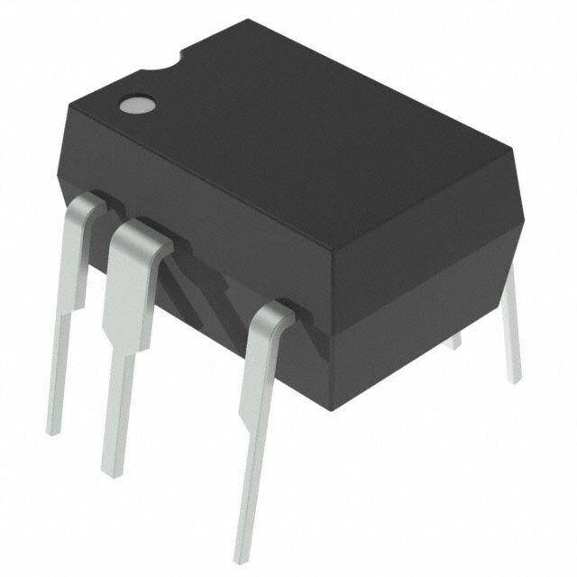
| 描述 | IC OFFLINE SWIT OTP OCP CV 8DIP |
| 产品分类 | |
| 品牌 | Power Integrations |
| 数据手册 | |
| 产品图片 |
|
| 产品型号 | LNK626PG |
| rohs | 无铅 / 符合限制有害物质指令(RoHS)规范要求 |
| 产品系列 | LinkSwitch®-CV |
| 产品目录页面 | |
| 供应商器件封装 | DIP-8C |
| 其它名称 | 596-1254-5 |
| 功率(W) | 17W |
| 包装 | 管件 |
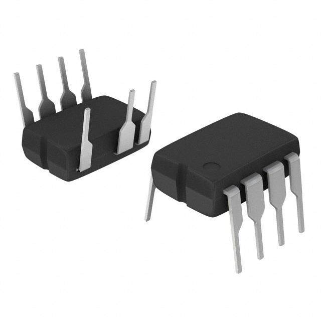
| 封装/外壳 | 8-DIP(0.300",7.62mm),7 引线 |
| 工作温度 | -40°C ~ 150°C |
| 标准包装 | 50 |
| 特色产品 | http://www.digikey.com/cn/zh/ph/PI/CV.html |
| 电压-击穿 | 700V |
| 电压-输入 | - |
| 电压-输出 | - |
| 输出隔离 | 隔离 |
| 配用 | /product-detail/zh/RDK-201/596-1266-ND/2058462 |
| 频率范围 | 93kHz ~ 106kHz |


- 商务部:美国ITC正式对集成电路等产品启动337调查
- 曝三星4nm工艺存在良率问题 高通将骁龙8 Gen1或转产台积电
- 太阳诱电将投资9.5亿元在常州建新厂生产MLCC 预计2023年完工
- 英特尔发布欧洲新工厂建设计划 深化IDM 2.0 战略
- 台积电先进制程称霸业界 有大客户加持明年业绩稳了
- 达到5530亿美元!SIA预计今年全球半导体销售额将创下新高
- 英特尔拟将自动驾驶子公司Mobileye上市 估值或超500亿美元
- 三星加码芯片和SET,合并消费电子和移动部门,撤换高东真等 CEO
- 三星电子宣布重大人事变动 还合并消费电子和移动部门
- 海关总署:前11个月进口集成电路产品价值2.52万亿元 增长14.8%


PDF Datasheet 数据手册内容提取
LNK623-626 LinkSwitch-CV Family Energy-Efficient, Off-line Switcher with Accurate Primary-side Constant-Voltage (CV) Control Product Highlights * Dramatically Simplifies CV Converters • Eliminates optocoupler and all secondary CV control circuitry • Eliminates bias winding supply – IC is self biasing Advanced Performance Features • Compensates for external component temperature variations Wide Range • Very tight IC parameter tolerances using proprietary trimming High-Voltage technology DC Input D FB • Continuous and/or discontinuous mode operation for design LinkSwitch-CV BP flexibility • Frequency jittering greatly reduces EMI filter cost S • Even tighter output tolerances achievable with external resistor selection/trimming PI-5195-012915 Advanced Protection/Safety Features (a) Typical Application Schematic • Auto-restart protection reduces delivered power by >95% for output short-circuit and all control loop faults (open and shorted VO ±5% components) • Hysteretic thermal shutdown – automatic recovery reduces power supply returns from the field • Meets HV creepage requirements between Drain and all other pins, both on the PCB and at the package E• cNooS-mloaadr ct™on–su Emnpetiorgn y< 2E0f0fi mciWen att 230 VAC and down to below A uto-R estart 70 mW with optional external bias PI-5196-012315 I • Easily meets all global energy efficiency regulations with no added O (b) Output Characteristic components • ON/OFF control provides constant efficiency down to very light Figure 1. Typical Application Schematic (a) and Output Characteristic Envelope (b). *Optional with LNK623-624PG/DG. (see Key Application Consider- loads – ideal for mandatory EISA and ENERGY STAR 2.0 regulations ations section for clamp and other external circuit design considerations). • No primary or secondary current sense resistors – maximizes efficiency Output Power Table Green Package 230 VAC ±15% 85-265 VAC • Halogen free and RoHS compliant package Product3 Peak or Peak or Applications Adapter1 Open Adapter1 Open Frame2 Frame2 • DVD/STB • Adapters LNK623PG/DG 6.5 W 9 W 5.0 W 6 W • Standby and auxiliary supplies LNK624PG/DG 7 W 11 W 5.5 W 6.5 W • Home appliances, white goods and consumer electronics LNK625PG/DG 8 W 13.5 W 6.5 W 8 W • Industrial controls LNK626PG/DG 10.5 W 17 W 8.5 W 10 W Description Table 1. Output Power Table. Based on 5 V Output. The LinkSwitchTM-CV dramatically simplifies low power, constant voltage Notes: (CV) converter design through a revolutionary control technique which 1. Minimum continuous power in a typical non-ventilated enclosed adapter eliminates the need for both an optocoupler and secondary CV control measured at +50 °C ambient. circuitry while providing very tight output voltage regulation. The 2. Maximum practical continuous power in an open frame design with adequate heat sinking, measured at 50 °C ambient (see Key Application Considerations combination of proprietary IC trimming and E-Shield™ transformer section for more information). construction techniques enables Clampless™ designs with the 3. Packages: P: DIP-8C, D: SO-8C. LinkSwitch-CV LNK623/4. LinkSwitch-CV provides excellent cross-regulation for multiple-output flyback applications such as DVDs and STBs. A 725 V power MOSFET and ON/OFF control state machine, self-biasing, frequency jittering, cycle-by-cycle current limit, and hysteretic thermal shutdown circuitry are all incorporated onto one IC. Figure 2. DIP-8C P and SO-8C D Packages. www.power.com August 2015 This Product is Covered by Patents and/or Pending Patent Applications.
LNK623-626 DRAIN (D) REGULATOR BYPASS 6 V (BP) + FB 6 V - + OUT Reset 5 V FEE(DFBBA)CK VTH - D Q MSATCAHTIENE V ILIMIT t SAMPLE-OUT I Drive LIM DC MAX FAULT 6.5 V FB Auto-Restart Open-Loop THERMAL SHUTDOWN DC MAX SAMPLE t DELAY SAMPLE-OUT OSCILLATOR SOURCE + (S) SOURCE ILIM - VILIMIT (S) Current Limit Comparator LEADING EDGE BLANKING PI-5197-012915 Figure 3 Functional Block Diagram. Pin Functional Description DRAIN (D) Pin: This pin is the power MOSFET drain connection. It provides internal P Package (DIP-8C) D Package (SO-8C) operating current for both start-up and steady-state operation. BYPASS (BP) Pin: This pin is the connection point for an external bypass capacitor for FB 1 8 S FB 1 8 S the internally generated 6 V supply. 2 7 BP 2 7 S BP S FEEDBACK (FB) Pin: 6 During normal operation, switching of the power MOSFET is 6 S S controlled by this pin. This pin senses the AC voltage on the bias 4 5 D S winding. This control input regulates the output voltage based on the D 4 5 S flyback voltage of the bias winding. SOURCE (S) Pin: This pin is internally connected to the output MOSFET source for PI-5198-012315 high-voltage power and control circuit common returns. Figure 4. Pin Configuration. 2 Rev. H 08/15 www.power.com
LNK623-626 LinkSwitch-CV Functional Description divider is open or missing) and reduces the auto-restart time from 200 ms to approximately 6 clock cycles (90 ms), whilst keeping the The LinkSwitch-CV combines a high-voltage power MOSFET switch disable period of 2.5 seconds. This effectively reduces the auto- with a power supply controller in one device. Similar to the restart duty cycle to less than 0.01%. LinkSwitch-LP and TinySwitch-III it uses ON/OFF control to regulate the output voltage. The LinkSwitch-CV controller consists of an Over-Temperature Protection oscillator, feedback (sense and logic) circuit, 6 V regulator, over- The thermal shutdown circuitry senses the die temperature. The temperature protection, frequency jittering, current limit circuit, threshold is set at 142 °C typical with a 60 °C hysteresis. When the leading-edge blanking, and ON/OFF state machine for CV control. die temperature rises above this threshold (142 °C) the power MOSFET is disabled and remains disabled until the die temperature Constant Voltage (CV) Operation falls by 60 °C, at which point the MOSFET is re-enabled. The controller regulates the FEEDBACK pin voltage to remain at V FBth using an ON/OFF state-machine. The FEEDBACK pin voltage is Current Limit sampled 2.5 ms after the turn-off of the high-voltage switch. At light The current limit circuit senses the current in the power MOSFET. loads the current limit is also reduced to decrease the transformer When this current exceeds the internal threshold (I ), the power LIMIT flux density. MOSFET is turned off for the remainder of that cycle. The leading edge blanking circuit inhibits the current limit comparator for a short Auto-Restart and Open-Loop Protection time (t ) after the power MOSFET is turned on. This leading edge In the event of a fault condition such as an output short or an open blankinLgEB time has been set so that current spikes caused by loop condition the LinkSwitch-CV enters into an appropriate capacitance and rectifier reverse recovery time will not cause protection mode as described below. premature termination of the MOSFET conduction. In the event the FEEDBACK pin voltage during the Flyback period falls 6.0 V Regulator below VFBth-0.3 V before the FEEDBACK pin sampling delay (~2.5 ms) The 6 V regulator charges the bypass capacitor connected to the for a duration in excess of 200 ms (auto-restart on-time (tAR-ON) the BYPASS pin to 6 V by drawing a current from the voltage on the converter enters into auto-restart, wherein the power MOSFET is DRAIN, whenever the MOSFET is off. The BYPASS pin is the internal disabled for 2.5 seconds (~8% auto-restart duty cycle). The auto-restart supply voltage node. When the MOSFET is on, the device runs off of alternately enables and disables the switching of the power MOSFET the energy stored in the bypass capacitor. Extremely low power until the fault condition is removed. consumption of the internal circuitry allows the LinkSwitch-CV to operate continuously from the current drawn from the DRAIN pin. In addition to the conditions for auto-restart described above, if the A bypass capacitor value of 1 mF is sufficient for both high frequency sensed FEEDBACK pin current during the Forward period of the decoupling and energy storage. conduction cycle (switch “on” time) falls below 120 mA, the converter annunciates this as an open-loop condition (top resistor in potential 3 www.power.com Rev. H 08/15
LNK623-626 Applications Example L1 3.5 × 7.6 mm T1 D8 Ferrite Bead EEL19 UF4003 12 V, 0.1 A 1 6 R1 C9 R8 51./18 kWΩ 82C03 pF 3 171 D7 SB540 4275 µVF 10L 3µH 12/48 k WΩ 5 V, 1.7 A FRD1106 FRD1206 1NV5R2712B 1 kV 8,9,10 4R71 0Ω 27C01 3pF 1010C008 VµF 417C001 0VµF 511/R807 WΩ D9 C11 R9 RTN UF4003 47 µF 39 kΩ R2 12 50 V 1/8 W 390 Ω F1 RV1 -22 V, 15 mA L 3.15 A 275 V 5 D5 1N4007 D6 85 - 265 C1 C2 1N4148 VAC 22 µF 22 µF 4 400 V 400 V N RT1 10 Ω 2 R3 6.34 kΩ LinkSwitch-CV 1% U1 D3 D4 LNK626PG 1N4007 1N4007 D FB BP S R4 R5 1C µ4F 6.2 kΩ 14/78 k WΩ 4.0R26 kΩ 10C 6µF 50 V C5 1% 50 V L2 680 pF 680 µH 50 V PI-5205-012315 Figure 5. 7 W (10 W peak) Multiple Output Flyback Converter for DVD Applications with Primary Sensed Feedback. Circuit Description The rectified and filtered input voltage is applied to one side of the This circuit is configured as a three output, primary-side regulated primary winding of T1. The other side of the transformer’s primary flyback power supply utilizing the LNK626PG. It can deliver 7 W winding is driven by the integrated MOSFET in U1. The leakage continuously and 10 W peak (thermally limited) from an universal inductance drain voltage spike is limited by the clamp circuit D5, R1, input voltage range (85 – 265 VAC). Efficiency is >67% at 115 R2, C3 and VR1. The Zener bleed clamp arrangement was selected VAC/230 VAC and no-load input power is <140 mW at 230 VAC. for lowest no-load input power but in applications where higher no-load input power is acceptable VR1 may be omitted and the value Input Filter of R1 increased to form a standard RCD clamp. AC input power is rectified by diodes D1 through D4. The rectified DC is filtered by the bulk storage capacitors C1 and C2. Inductor L1, Output Rectification L2, C1 and C2 form a pi (π) filter, which attenuates conducted The secondaries of the transformer are rectified by D7, D8 and D9. differential-mode EMI noise. This configuration along with Power A Schottky barrier type was used for the main 5 V output for higher Integrations transformer E-shield technology allow this design to efficiency. The +12 V and -22 V outputs use an ultrafast rectifier meet EMI standard EN55022 class B with good margin without diode. The main output is post filtered by L3 and C10 to remove requiring a Y capacitor. Fuse F1 provides protection against switching frequency ripple. Resistors R7, R8 and R9 provide a catastrophic failure. Negative temperature coefficient thermistor RT1 preload to maintain the output voltages within their respective limits limits the inrush current when AC is first applied to below the when unloaded. To reduce high frequency ringing and associated maximum rating of diodes D1 through D4. Metal oxide varistor RV1 radiated EMI an RC snubber formed by R10 and C13 was added clamps the AC input during differential line transients, protecting the across D7. input components and maintaining the peak drain voltage of U1 Output Regulation below its 725 V BV rating. For differential surge levels at or below DSS The LNK626 regulates the output using ON/OFF control, enabling or 2 kV this component may be omitted. disabling switching cycles based on the sampled voltage on the LNK626 Primary FEEDBACK pin. The output voltage is sensed using a primary The LNK626PG device (U1) incorporates the power switching device, referenced winding on transformer T1 eliminating the need for an oscillator, CV control engine, startup, and protection functions. The optocoupler and a secondary sense circuit. The resistor divider formed integrated 725 V MOSFET provides a large drain voltage margin in by R3 and R6 feeds the winding voltage into U1. Standard 1% resistor universal input AC applications, increasing reliability and also reducing values were used to center the nominal output voltages. Resistor R5 the output diode voltage stress by allowing a greater transformer and C5 reduce pulse grouping by creating an offset voltage that is turns ratio. The device can be completely self-powered from the proportional to the number of consecutive enabled switching cycles. BYPASS pin and decoupling capacitor C4. In this design a bias circuit (D6, C6 and R4) was added to reduce no load input power below 140 mW. 4 Rev. H 08/15 www.power.com
LNK623-626 Key Application Considerations Single Point Grounding Use a single point (Kelvin) connection at the negative terminal of the Output Power Table input filter capacitor for the LinkSwitch-CV SOURCE pin and bias The data sheet maximum output power table (Table 1) represents the winding return. This improves surge capabilities by returning surge maximum practical continuous output power level that can be obtained currents from the bias winding directly to the input filter capacitor. in a Flyback converter under the following assumed conditions: Bypass Capacitor 1. The minimum DC input voltage is 100 V or higher at 90 VAC input. The BYPASS pin capacitor should be located as close as possible to The value of the input capacitance should be large enough to the SOURCE and BYPASS pins. meet these criteria for AC input designs. 2. Secondary output of 5 V with a Schottky rectifier diode. Feedback Resistors 3. Assumed efficiency of 80%. Place the feedback resistors directly at the FEEDBACK pin of the 4. Continuous conduction mode operation (K = 0.4). LinkSwitch-CV device. This minimizes noise coupling. P 5. Reflected Output Voltage (V ) of 110 V. OR Thermal Considerations 6. The part is board mounted with SOURCE pins soldered to a The copper area connected to the SOURCE pins provide the sufficient area of copper to keep the SOURCE pin temperature at LinkSwitch-CV heat sink. A rule of thumb estimate is that the or below 110 °C for P package and 100 °C for D packaged LinkSwitch-CV will dissipate 10% of the output power. Provide devices. enough copper area to keep the SOURCE pin temperature below 7. Ambient temperature of 50 °C for open frame designs and an 110° C to provide margin for part to part R variation. internal enclosure temperature of 60 °C for adapter designs. DS(ON) Secondary Loop Area Note: Higher output power are achievable if the efficiency is higher To minimize leakage inductance and EMI, the area of the loop than 80%, typically for high output voltage designs. connecting the secondary winding, the output diode and the output BYPASS Pin Capacitor filter capacitor should be minimized. In addition, sufficient copper A 1 mF BYPASS pin capacitor (C4) is recommended. The capacitor area should be provided at the anode and cathode terminal of the diode for heat sinking. A larger area is preferred at the quiet cathode voltage rating should be equal to or greater than 6.8 V. The terminal. A large anode area can increase high frequency radiated EMI. capacitor’s dielectric material is not important. The capacitor must be physically located close to the LinkSwitch-CV BYPASS pin. Electrostatic Discharge Spark Gap In chargers and adapters ESD discharges may be applied to the Circuit board layout output of the supply. In these applications the addition of a spark LinkSwitch-CV is a highly integrated power supply solution that gap is recommended. A trace is placed along the isolation barrier to integrates on a single die, both the controller and the high-voltage form one electrode of a spark gap. The other electrode, on the MOSFET. The presence of high switching currents and voltages secondary side, is formed by the output return node. The arrange- together with analog signals makes it especially important to follow ment directs ESD energy from the secondary to the primary side AC good PCB design practice to ensure stable and trouble free operation input. A 10 mil gap is placed near the AC input. The gap decouples of the power supply. any noise picked up on the spark gap trace to the AC input. The When designing a board for the LinkSwitch-CV based power supply, it trace from the AC input to the spark gap electrode should be spaced is important to follow the following guidelines: away from other traces to prevent unwanted arcing occurring and possible circuit damage. 5 www.power.com Rev. H 08/15
LNK623-626 Primary Side Secondary Side Drain trace area miniminzed Output Filter Input Filter Clamp Output Capacitor Capacitor Components Isolation Barrier Rectifiers C1 VR1R2 Y1 C11 Copper area C3 Capacitor C12 maximized for L1 T1 (optional) D9 heat sinking R10 C13 D7 R1 D5 L3 C2 U1 D1 D3 S D L2 Transformer C8 S BP R3 S D4 D2 S JP1 C10 FB R4 C4 C9 D8 R8 R9 F1 RV1 C5 R7 R5 D6 R6 C6 J2 RT1 J1 1 6 ESD spark gap 10 mil Bypass Feedback DC Outputs + AC - gap Capacitor Resistors close IN close to device to device PI-5269-012315 Figure 6. PCB Layout Example. B+ B+ CLAMP CLAMP Small FEEDBACK pin node area D D FB FB BP BP S Bias resistor S Minimize FEEDBACK pin node PRI RTN PRI RTN area Bias currents Kelvin connection at PI-5266-012315 Bias currents Kelvin connection at PI-5265-012315 return to bulk SOURCE pin, no power return to bulk SOURCE pin, no power capacitor currents in signal traces capacitor currents in signal traces Figure 7. Schematic Representation of Recommended Layout Without Figure 8. Schematic Representation of Recommended Layout With External Bias. External Bias. 6 Rev. H 08/15 www.power.com
LNK623-626 B+ CLAMP Drain trace in close proximity of feedback trace will couple noise into feedback signal Power currents flow in signal source trace D FB BP Trace S Isource PRI RTN impedance Line surge Bias winding currents can currents flow in flow through ∆V signal source traces device S Voltage drops across trace impedance PI-5267-012615 may cause degraded performance Figure 9. Schematic Representation of Electrical Impact of Improper Layout. 7 www.power.com Rev. H 08/15
LNK623-626 Drain Clamp Recommended Clamp Circuits RC2 CC1 RC2 C C1 D C2 R C1 R C1 D C1 D C1 PI-5107-012615 PI-5108-110308 Figure 10. RCD Clamp, Low Power or Low Leakage Inductance Designs. RCD Clamp With Zener Bleed. High Power or High Leakage Inductance Designs. Components R1, R2, C3, VR1 and D5 in Figure 5 comprise the clamp. This circuit is preferred when the primary leakage inductance is greater than 125 mH to reduce drain voltage overshoot or ringing present on the feedback winding. For best output regulation, the feedback R C C2 C1 voltage must settle to within 1% at 2.1 ms from the turn off of the primary MOSFET. This requires careful selection of the clamp circuit components. The voltage of VR1 is selected to be ~20% above the R reflected output voltage (V ). This is to clip any turn off spike on the C1 OR drain but avoid conduction during the flyback voltage interval when the D C1 output diode is conducting. The value of R1 should be the largest value that results in acceptable settling of the FEEDBACK pin voltage and peak drain voltage. Making R1 too large will increase the discharge time of C3 and degrade regulation. Resistor R2 dampens the leakage inductance ring. The value must be large enough to dampen the ring in the required time but must not be too large to cause the drain PI-5107-012615 voltage to exceed 680 V. If the primary leakage inductance is less than 125 mH, VR1 can be eliminated and the value of R1 increased. A value of 470 kW with an 820 pF capacitor is a recommended starting point. Verify that the peak drain voltage is less than 680 V under all line and load conditions. Verify the feedback winding settles to an acceptable limit for good line and load regulation. Effect of Fast (500 ns) versus Slow (2 ms) Recovery Diodes in Clamp Circuit on Pulse Grouping and Output Ripple. A slow reverse recovery diode reduces the feedback voltage ringing. The amplitude of ringing with a fast diode represents 8% error in Figure 11. Black Trace: D is a FR107 (fast type, trr = 500 ns) C1 Gray Trace: D is a 1N4007G (standard recovery, trr = 2 us) C1 Figure 11. Effect of Clamp Diode on FEEDBACK Pin Settling. Clamp Circuit (top). FEEDBACK Pin Voltage (bottom). 8 Rev. H 08/15 www.power.com
LNK623-626 Clampless Designs To eliminate group pulsing verify that the feedback signal settles Clampless designs rely solely on the drain node capacitance to limit within 2.1 ms from the turn off of the internal MOSFET. A Zener diode the leakage inductance induced peak drain-to-source voltage. in the clamp circuit may be needed to achieve the desired settling Therefore the maximum AC input line voltage, the value of V , the time. If the settling time is satisfactory, then a RC network across OR leakage inductance energy, (a function of leakage inductance and R (R6) of the feedback resistors is necessary. LOWER peak primary current), and the primary winding capacitance determine The value of R (R5 in the Figure 13) should be an order of magnitude the peak drain voltage. With no significant dissipative element greater than R and selected such that R×C = 32 ms where C is present, as is the case with an external clamp, the longer duration of LOWER C5 in Figure 13. the leakage inductance ringing can increase EMI. Quick Design Checklist The following requirements are recommended for a universal input or 230 VAC only Clampless design: As with any power supply design, all LinkSwitch-CV designs should be verified on the bench to make sure that component specifications are 1. Clampless designs should only be used for P ≤5 W using a V O OR not exceeded under worst-case conditions. The following minimum of ≤90 V set of tests is strongly recommended: 2. For designs with P ≤5 W, a two-layer primary must be used to O ensure adequate primary intra-winding capacitance in the range 1. Maximum drain voltage – Verify that peak V does not exceed DS of 25 pF to 50 pF. A bias winding must be added to the trans- 680 V at highest input voltage and maximum output power. former using a standard recovery rectifier diode (1N4003– 1N4007) to act as a clamp. This bias winding may also be used to externally power the device by connecting a resistor from the 5 bias winding capacitor to the BYPASS pin. This inhibits the D6 internal high-voltage current source, reducing device dissipation 1N4148 and no-load consumption. 4 3. For designs with P >5 W, Clampless designs are not practical and O an external RCD or Zener clamp should be used. 4. Ensure that worst-case, high line, peak drain voltage is below the 2 R3 BV specification of the internal MOSFET and ideally ≤650 V to LinkSwitch-CV 6.34 kΩ DSS U1 1% allow margin for design variation. LNK626PG D V (Reflected Output Voltage), is the secondary output plus output FB OR diode forward voltage drop that is reflected to the primary via the BP turns ratio of the transformer during the diode conduction time. The S R4 R5 V adds to the DC bus voltage and the leakage spike to determine the 6.2 kΩ 47 kΩ OR C4 1/8 W R6 C6 peak drain voltage. 1 µF 4.02 kΩ 10 µF 50 V C5 1% 50 V 680 pF Pulse Grouping 50 V Pulse grouping is defined as 6 or more consecutive pulses followed by two or more timing state changes. The effect of pulse grouping is PI-5268-110608 increased output voltage ripple. This is shown on the right of Figure 12 where pulse grouping has caused an increase in the output ripple. Figure 13. RC Network Across R (R6) to Reduce Pulse Grouping. BOTTOM TToopp TTrraaccee:: DDrraaiinn WWaavveeffoorrmm ((220000 VV//ddiivv)) SSpplliitt SSccrreeeenn wwiitthh BBoottttoomm SSccrreeeenn ZZoooomm BBoottttoomm TTrraaccee:: OOuuttppuutt RRiippppllee VVoollttaaggee ((5500 mmVV//ddiivv)) TToopp TTrraaccee:: DDrraaiinn WWaavveeffoorrmm ((220000 VV//ddiivv)) BBoottttoomm TTrraaccee:: OOuuttppuutt RRiippppllee VVoollttaaggee ((5500 mmVV//ddiivv)) Figure 12. Not Pulse Grouping (<5 Consecutive Switching Cycles). Pulse Grouping (>5 Consecutive Switching Cycles). 9 www.power.com Rev. H 08/15
LNK623-626 2. Maximum drain current – At maximum ambient temperature, LinkSwitch-CV, transformer, output diodes and output capacitors. maximum input voltage and maximum output load, verify drain Enough thermal margin should be allowed for the part-to-part current waveforms at start-up for any signs of transformer variation of the R of LinkSwitch-CV, as specified in the data DS(ON) saturation and excessive leading edge current spikes. LinkSwitch-CV sheet. It is recommended that the maximum SOURCE pin has a leading edge blanking time of 215 ns to prevent premature temperature does not exceed 110 °C. termination of the ON-cycle. Verify that the leading edge current Design Tools spike is below the allowed current limit envelope for the drain current waveform at the end of the 215 ns blanking period. Up-to-date information on design tools can be found at the Power 3. Thermal check – At maximum output power, both minimum and Integrations web site: www.power.com maximum input voltage and maximum ambient temperature; verify that temperature specifications are not exceeded for 10 Rev. H 08/15 www.power.com
LNK623-626 Absolute Maximum Ratings1,5 DRAIN Voltage ........................................................-0.3 V to 725 V Notes: DRAIN Peak Current: LNK623 .................................400 (600) mA4 1. All voltages referenced to SOURCE, T = 25 °C. A LNK624 .................................400 (600) mA4 2. Duration not to exceed 2 msec. LNK625 .................................528 (790) mA4 3. 1/16 in. from case for 5 seconds. LNK626 ...............................720 (1080) mA4 4. The higher peak DRAIN current is allowed while the DRAIN Peak Negative Pulsed DRAIN Current .................................-100 mA2 voltage is simultaneously less than 400 V. Feedback Pin Voltage ..................................................-0.3 V to 9 V 5. Maximum ratings specified may be applied, one at a time Feedback Pin Current ..........................................................100 mA without causing permanent damage to the product. BYPASS Pin Voltage ....................................................-0.3 V to 9 V Exposure to Absolute Maximum ratings for extended BYPASS Pin Current ...............................................................10 mA periods of time may affect product reliability. Storage Temperature ...................................... ..........-65 °C to 150 °C Operating Junction Temperature ..............................-40 °C to 150 °C Lead Temperature(3) ..............................................................260 °C Thermal Resistance Thermal Resistance: P Package: Notes: (q ) .......................... ..............70 °C/W2; 60 °C/W3 1. Measured on pin 8 (SOURCE) close to plastic interface. JA (q )1 ......................................................11 °C/W 2. Soldered to 0.36 sq. in. (232 mm2), 2 oz. (610 g/m2) copper clad. JC D Package: 3. Soldered to 1 sq. in. (645 mm2), 2 oz. (610 g/m2) copper clad. (q ) .....................................100 °C/W2; 80 °C/W3 JA (q )1 .......................................................30 °C/W JC Conditions Parameter Symbol SOURCE = 0 V; T = -40 to 125 °C Min Typ Max Units J (Unless Otherwise Specified) Control Functions Output Frequency f T = 25 °C, V = V LNK623/6 93 100 106 kHz OSC J FB FBth Peak-Peak Jitter Compared to Frequency Jitter ±7 % Average Frequency, T = 25 °C J Ratio of Output T = 25 °C Frequency at Auto- f J 80 % OSC(AR) Relative to f , See Note C Restart OSC T = 25 °C Maximum Duty Cycle DC J 54 % MAX See Notes B, C LNK623-624P 1.815 1.840 1.865 T = 25 °C J LNK623-624D 1.855 1.880 1.905 See Figure 15 FEEDBACK Pin Voltage V V FBth C = 1 mF BP LNK625P, LNK625D 1.835 1.860 1.885 See Note D LNK626P, LNK626D 1.775 1.800 1.825 FEEDBACK Pin Voltage Temperature TC -0.01 %/°C VFB Coefficient FEEDBACK Pin Voltage V 1.45 V at Turn-Off Threshold FB(AR) LNK623/6P I2f = I2 × f 0.9 × I2f I2f 1.17 × I2f LIMIT(TYP) OSC(TYP) T = 25 °C J Power Coefficient I2f A2Hz LNK623/6D I2f = I2 × f 0.9 × I2f I2f 1.21 × I2f LIMIT(TYP) OSC(TYP) T = 25 °C J 11 www.power.com Rev. H 08/15
LNK623-626 Conditions Parameter Symbol SOURCE = 0 V; T = -40 to 125 °C Min Typ Max Units J (Unless Otherwise Specified) Control Functions (cont.) Minimum Switch t See Note C 700 ns “On”-Time ON(min) FEEDBACK Pin t 2.35 2.55 2.75 ms Sampling Delay FB IS1 FB Voltage > VFBth 280 330 LNK623/4 440 520 DRAIN Supply FB Voltage = V -0.1, mA Current FBth I Switch ON-Time = t (MOSFET LNK625 480 560 S2 ON Switching at f ) OSC LNK626 520 600 LNK623/4 -5.0 -3.4 -1.8 I V = 0 V CH1 BP LNK625/6 -7.0 -4.5 -2.0 BYPASS Pin mA Charge Current LNK623/4 -4.0 -2.3 -1.0 I V = 4 V CH2 BP LNK625/6 -5.6 -3.2 -1.4 BYPASS Pin Voltage V 5.65 6.00 6.25 V BP BYPASS Pin V 0.70 1.00 1.20 V Voltage Hysteresis BPH BYPASS Pin V 6.2 6.5 6.8 V Shunt Voltage SHUNT Circuit Protection LNK623 196 210 225 di/dt = 50 mA/ms , T = 25 °C J LNK624 233 250 268 di/dt = 60 mA/ms , T = 25 °C J Current Limit I mA LIMIT LNK625 307 330 353 di/dt = 80 mA/ms , T = 25 °C J LNK626 419 450 482 di/dt = 110 mA/ms , T = 25 °C J Leading Edge T = 25 °C t J 170 215 ns Blanking Time LEB See Note C Thermal Shutdown T 135 142 150 °C Temperature SD Thermal Shutdown T 60 °C Hysteresis SDH 12 Rev. H 08/15 www.power.com
LNK623-626 Conditions Parameter Symbol SOURCE = 0 V; T = -40 to 125 °C Min Typ Max Units J (Unless Otherwise Specified) Output T = 25 °C 24 28 LNK623 J I = 50 mA D T = 100 °C 36 42 J T = 25 °C 24 28 LNK624 J I = 50 mA ON-State D TJ = 100 °C 36 42 R W Resistance DS(ON) T = 25 °C 16 19 LNK625 J I = 62 mA D T = 100 °C 24 28 J T = 25 °C 9.6 11 LNK626 J I = 82 mA D T = 100 °C 14 17 J V = 560 V, See Figure 20 I DS 50 DSS1 T = 125 °C, See Note A OFF-State J mA Leakage V = 375 V, See Figure 20 I DS 15 DSS2 T = 50 °C J Breakdown T = 25 °C BV J 725 V Voltage DSS See Figure 20 DRAIN Supply 50 V Voltage Auto-Restart V = 0 t FB 200 ms ON-Time AR-ON See Note C LNK623/624/626 2 s Auto-Restart t OFF-Time AR-OFF LNK625 1 Open-Loop FEEDBACK Pin I See Note C -120 mA OL Current Threshold Open-Loop See Note C 90 ms ON-Time NOTES: A. I is the worst-case OFF-state leakage specification at 80% of BV and maximum operating junction temperature. I is a typical DSS1 DSS DSS2 specification under worst-case application conditions (rectified 265 VAC) for no-load consumption calculations. B. When the duty cycle exceeds DC the LinkSwitch-CV operates in on-time extension mode. MAX C. This parameter is derived from characterization. D. Mechanical stress induced during the assembly may cause shift in this parameter. This shift has not impact on the ability of LinkSwitch-CV to meet CV = ±5% in mass production given the design follows recommendation in AN-45 and good manufacturing practice. 13 www.power.com Rev. H 08/15
LNK623-626 Typical Performance Characteristics 1.200 1.200 °C)1.000 PI-5086-012315 e°C)1.000 PI-5089-012315 cyo 25 0.800 oltago 25 0.800 Frequenmalized t00..640000 edback Vmalized t00..640000 r er o Fo N N (0.200 (0.200 0.000 0.000 -40 -15 10 35 60 85 110 135 -40 -15 10 35 60 85 110 135 Temperature (°C) Temperature (°C) Figure 14. Output Frequency vs. Temperature. Figure 15. Feedback Voltage vs. Temperature. geC)°1.1 PI-2213-012315 A) 320500 TTCCAASSEE==2150 0° C°C PI-5211-080708 a5 m Breakdown VoltNormalized to 21.0 Drain Current ( 211005000 LSNcaKl6in2g3 Fact1o.r0s: ( 50 LNK624 1.0 LNK625 1.5 LNK626 2.5 0.9 0 -50 -25 0 25 50 75 100 125 150 0 2 4 6 8 10 Junction Temperature (°C) DRAIN Voltage (V) Figure 16. Breakdown vs. Temperature. Figure 17. Output Characteristic. (pF) 1000 LLLLSNNNNcaKKKKl6666in2222g3456 Fact1112o....r0055s : PI-5201-012615 5400 LLLLSNNNNcaKKKKl6666in2222g3456 Fact1112o....r0055s : PI-5212-012615 ce 100 W) an m 30 acit er ( p w 20 a n C 10 Po rai 10 D 1 0 0 100 200 300 400 500 600 0 200 400 600 Drain Voltage (V) DRAIN Voltage (V) Figure 18. C vs. Drain Voltage. Figure 19. Drain Capacitance Power. OSS 14 Rev. H 08/15 www.power.com
LNK623-626 LinkSwitch-CV FB S 5 µF 50 kΩ 10 kΩ 1 µF BP S .1 µF S D S 4 kΩ S1 S2 V IN + 16 V Curve Tracer To measure BV , I , and I follow these steps: DSS DSS1 DSS2 1) Close S1, open S2 2) Power-up V source (16 V) IN 3) Open S1, close S2 4) Measure I/V characteristics of DRAIN pin using the curve tracer PI-5203-012615 Figure 20. Test Set-up for Leakage and Breakdown Tests. 15 www.power.com Rev. H 08/15
LNK623-626 PDIP-8C (P Package) ⊕D S.004 (.10) Notes: -E- 1. Package dimensions conform to JEDEC specification MS-001-AB (Issue B 7/85) for standard dual-in-line (DIP) package with .300 inch row spacing. 2. Controlling dimensions are inches. Millimeter sizes are shown in parentheses. .240 (6.10) 3. Dimensions shown do not include mold flash or other .260 (6.60) protrusions. Mold flash or protrusions shall not exceed .006 (.15) on any side. 4. Pin locations start with Pin 1, and continue counter-clock- wise to Pin 8 when viewed from the top. The notch and/or dimple are aids in locating Pin 1. Pin 3 is omitted. Pin 1 5. Minimum metal to metal spacing at the package body for the omitted lead location is .137 inch (3.48 mm). .367 (9.32) -D- 6. Lead width measured at package body. .387 (9.83) 7. Lead spacing measured with the leads constrained to be .057 (1.45) perpendicular to plane T. .068 (1.73) (NOTE 6) .125 (3.18) .015 (.38) .145 (3.68) MINIMUM -T- SEATING .008 (.20) PLANE .120 (3.05) .015 (.38) .140 (3.56) .300 (7.62) BSC .100 (2.54) BSC .048 (1.22) .137 (3.48) (NOTE 7) .053 (1.35) MINIMUM P08C .014 (.36) .300 (7.62) .022 (.56) ⊕T E D S .010 (.25) M .390 (9.91) PI-3933-012315 16 Rev. H 08/15 www.power.com
LNK623-626 SO-8C (D Package) 0.10 (0.004) C A-B2X 2 DETAIL A 4 B 4.90 (0.193) BSC A 4 D 8 5 GAUGE PLANE SEATING PLANE 2 3.90 (0.154) BSC 6.00 (0.236) BSC C 0 - 8o 0.25 (0.010) 1.04 (0.041) REF BSC 0.10 (0.004) C D 0.40 (0.016) 2X Pin 1 ID 1 4 0.20 (0.008) C 1.27 (0.050) 1.27 (0.050) BSC 2X 7X 0.31 - 0.51 (0.012 - 0.020) 0.25 (0.010) M CA-BD 1.35 (0.053) 1.25 - 1.65 DETAIL A 1.75 (0.069) (0.049 - 0.065) 0.10 (0.004) 0.10 (0.004) C H 0.25 (0.010) 7X SEATING PLANE 0.17 (0.007) C 0.25 (0.010) Reference Solder Pad + Dimensions Notes: 1. JEDEC reference: MS-012. 2.00 (0.079) 4.90 (0.193) 2. Package outline exclusive of mold flash and metal burr. 3. Package outline inclusive of plating thickness. 4. Datums A and B to be determined at datum plane H. + + + 5. Controlling dimensions are in millimeters. Inch dimensions are shown in parenthesis. Angles in degrees. D07C 1.27 (0.050) 0.60 (0.024) PI-4526-012315 Part Ordering Information • LinkSwitch Product Family • CV Series Number • Package Identifier P Plastic DIP D Plastic SO-8 • Package Material G GREEN: Halogen Free and RoHS Compliant • Tape & Reel and Other Options Blank Standard Configurations LNK 625 D G - TL TL Tape & Reel, 2.5 k pcs for D Package. Not available for P Package. 17 www.power.com Rev. H 08/15
Revision Notes Date B Release data sheet. 11/08 C Correction made to Figure 5. 12/08 D Introduced Max Current Limit when V DRAIN is below 400 V. 07/09 E Introduced LNK626DG. 09/09 F Added Note 4 to Parameter Table 02/10 F Specified Max BYPASS Pin Current. 03/14 Figure removed “Test Set-up for FEEDBACK Pin Measurements” from previous version. Updated t parameter. G AR-OFF 02/15 Updated to latest Brand Style. H Update BV from 700 V to 725 V 08/15 DSS For the latest updates, visit our website: www.power.com Power Integrations reserves the right to make changes to its products at any time to improve reliability or manufacturability. Power Integrations does not assume any liability arising from the use of any device or circuit described herein. POWER INTEGRATIONS MAKES NO WARRANTY HEREIN AND SPECIFICALLY DISCLAIMS ALL WARRANTIES INCLUDING, WITHOUT LIMITATION, THE IMPLIED WARRANTIES OF MERCHANTABILITY, FITNESS FOR A PARTICULAR PURPOSE, AND NON-INFRINGEMENT OF THIRD PARTY RIGHTS. Patent Information The products and applications illustrated herein (including transformer construction and circuits external to the products) may be covered by one or more U.S. and foreign patents, or potentially by pending U.S. and foreign patent applications assigned to Power Integrations. A complete list of Power Integrations patents may be found at www.power.com. Power Integrations grants its customers a license under certain patent rights as set forth at http://www.power.com/ip.htm. Life Support Policy POWER INTEGRATIONS PRODUCTS ARE NOT AUTHORIZED FOR USE AS CRITICAL COMPONENTS IN LIFE SUPPORT DEVICES OR SYSTEMS WITHOUT THE EXPRESS WRITTEN APPROVAL OF THE PRESIDENT OF POWER INTEGRATIONS. As used herein: 1. A Life support device or system is one which, (i) is intended for surgical implant into the body, or (ii) supports or sustains life, and (iii) whose failure to perform, when properly used in accordance with instructions for use, can be reasonably expected to result in significant injury or death to the user. 2. A critical component is any component of a life support device or system whose failure to perform can be reasonably expected to cause the failure of the life support device or system, or to affect its safety or effectiveness. The PI logo, TOPSwitch, TinySwitch, LinkSwitch, LYTSwitch, InnoSwitch, DPA-Switch, PeakSwitch, CAPZero, SENZero, LinkZero, HiperPFS, HiperTFS, HiperLCS, Qspeed, EcoSmart, Clampless, E-Shield, Filterfuse, FluxLink, StakFET, PI Expert and PI FACTS are trademarks of Power Integrations, Inc. Other trademarks are property of their respective companies. ©2015, Power Integrations, Inc. Power Integrations Worldwide Sales Support Locations World Headquarters Germany Japan Taiwan 5245 Hellyer Avenue Lindwurmstrasse 114 Kosei Dai-3 Bldg. 5F, No. 318, Nei Hu Rd., Sec. 1 San Jose, CA 95138, USA. 80337 Munich 2-12-11, Shin-Yokohama, Nei Hu Dist. Main: +1-408-414-9200 Germany Kohoku-ku Taipei 11493, Taiwan R.O.C. Customer Service: Phone: +49-895-527-39110 Yokohama-shi Kanagwan Phone: +886-2-2659-4570 Phone: +1-408-414-9665 Fax: +49-895-527-39200 222-0033 Japan Fax: +886-2-2659-4550 Fax: +1-408-414-9765 e-mail: eurosales@power.com Phone: +81-45-471-1021 e-mail: taiwansales@power.com e-mail: usasales@power.com Fax: +81-45-471-3717 India e-mail: japansales@power.com UK China (Shanghai) #1, 14th Main Road Cambridge Semiconductor, Rm 2410, Charity Plaza, No. 88 Vasanthanagar Korea a Power Integrations company North Caoxi Road Bangalore-560052 India RM 602, 6FL Westbrook Centre, Block 5, 2nd Floor Shanghai, PRC 200030 Phone: +91-80-4113-8020 Korea City Air Terminal B/D, 159-6 Milton Road Phone: +86-21-6354-6323 Fax: +91-80-4113-8023 Samsung-Dong, Kangnam-Gu, Cambridge CB4 1YG Fax: +86-21-6354-6325 e-mail: indiasales@power.com Seoul, 135-728, Korea Phone: +44 (0) 1223-446483 e-mail: chinasales@power.com Phone: +82-2-2016-6610 e-mail: eurosales@power.com Italy Fax: +82-2-2016-6630 China (Shenzhen) Via Milanese 20, 3rd. Fl. e-mail: koreasales@power.com 17/F, Hivac Building, No. 2, Keji Nan 20099 Sesto San Giovanni (MI) 8th Road, Nanshan District, Italy Singapore Shenzhen, China, 518057 Phone: +39-024-550-8701 51 Newton Road Phone: +86-755-8672-8689 Fax: +39-028-928-6009 #19-01/05 Goldhill Plaza Fax: +86-755-8672-8690 e-mail: eurosales@power.com Singapore, 308900 e-mail: chinasales@power.com Phone: +65-6358-2160 Fax: +65-6358-2015 e-mail: singaporesales@power.com
Mouser Electronics Authorized Distributor Click to View Pricing, Inventory, Delivery & Lifecycle Information: P ower Integrations: LNK623PG LNK623DG LNK623DG-TL LNK624PG LNK624DG LNK624DG-TL LNK625PG LNK625DG LNK625DG-TL LNK626PG LNK626DG