ICGOO在线商城 > 射频/IF 和 RFID > RF 收发器 IC > JN5161/001,515

 Datasheet下载
- 型号: JN5161/001,515
- 制造商: NXP Semiconductors
- 库位|库存: xxxx|xxxx
- 要求:
| 数量阶梯 | 香港交货 | 国内含税 |
| +xxxx | $xxxx | ¥xxxx |
查看当月历史价格
查看今年历史价格
JN5161/001,515产品简介:
ICGOO电子元器件商城为您提供JN5161/001,515由NXP Semiconductors设计生产,在icgoo商城现货销售,并且可以通过原厂、代理商等渠道进行代购。 JN5161/001,515价格参考。NXP SemiconductorsJN5161/001,515封装/规格:RF 收发器 IC, IC 射频 TxRx + MCU 802.15.4 ZigbeePRO® 2.4GHz 40-VFQFN 裸露焊盘。您可以下载JN5161/001,515参考资料、Datasheet数据手册功能说明书,资料中有JN5161/001,515 详细功能的应用电路图电压和使用方法及教程。
NXP USA Inc. 生产的型号为 JN5161/001,515 的 RF 收发器 IC 是一款基于 IEEE 802.15.4 标准的低功耗无线通信芯片,主要应用于 Zigbee 和 JenNet-IP 等物联网协议栈。以下是其主要应用场景:

 1. 智能家居
   - 智能照明:用于控制灯光的开关、亮度调节和颜色变化,实现远程或自动化管理。
   - 环境监测:通过传感器网络监控温度、湿度、空气质量等环境参数。
   - 安防系统:支持门窗传感器、运动检测器和烟雾报警器等设备的无线连接。

 2. 工业自动化
   - 传感器网络:在工业环境中采集数据(如压力、流量、振动等),并传输到中央控制系统。
   - 设备监控:实时监测生产设备的状态,预测故障并优化维护计划。
   - 无线控制:用于工厂内设备的无线控制,减少布线需求,提高灵活性。

 3. 医疗健康
   - 可穿戴设备:如心率监测器、血糖仪等,将健康数据传输到手机或云端进行分析。
   - 远程监护:通过无线网络将患者的生命体征数据发送给医护人员。

 4. 楼宇自动化
   - 能源管理:监控和优化建筑物内的电力、水力和暖通空调(HVAC)系统的使用。
   - 门禁控制:实现无线门锁、考勤系统等功能。
   - 环境调控:根据传感器反馈自动调整室内温湿度和光照。

 5. 消费电子
   - 遥控器:用于家电设备的无线控制,替代传统的红外遥控。
   - 玩具与游戏:支持互动式玩具和多人在线游戏的无线通信。

 6. 农业物联网
   - 精准农业:监测土壤湿度、作物生长情况以及气象条件,帮助农民优化种植策略。
   - 牲畜跟踪:通过无线标签跟踪牲畜的位置和健康状况。

JN5161/001,515 的低功耗特性使其非常适合电池供电的设备,而其强大的处理能力和丰富的外设接口则能够满足复杂的应用需求。这款芯片广泛应用于需要稳定、可靠且低延迟无线通信的场景中。
| 参数 | 数值 |
| 产品目录 | |
| 描述 | MCU TXRX IEEE802.15.4 40HVQFN射频微控制器 - MCU IEEE802.15.4 Wireless MCU |
| 产品分类 | RF 收发器集成电路 - IC |
| 品牌 | NXP Semiconductors |
| 产品手册 | |
| 产品图片 |
|
| 产品系列 | 嵌入式处理器和控制器,微控制器 - MCU,射频微控制器 - MCU,NXP Semiconductors JN5161/001,515- |
| mouser_ship_limit | 此产品可能需要其他文件才能从美国出口。 |
| 数据手册 | |
| 产品型号 | JN5161/001,515 |
| rohs | 无铅 / 符合限制有害物质指令(RoHS)规范要求 |
| 产品种类 | 射频微控制器 - MCU |
| 其它名称 | 568-10147-1 |
| 功率-输出 | 2.5dBm |
| 包装 | 剪切带 (CT) |
| 可用A/D通道 | 4 |
| 可编程输入/输出端数量 | 20 |
| 商标 | NXP Semiconductors |
| 处理器系列 | JN516x |
| 天线连接器 | PCB,表面贴装 |
| 存储容量 | 64kB 闪存, 8kB RAM, 4kB EEPROM |
| 安装风格 | SMD/SMT |
| 定时器数量 | 3 Timer |
| 封装 | Reel |
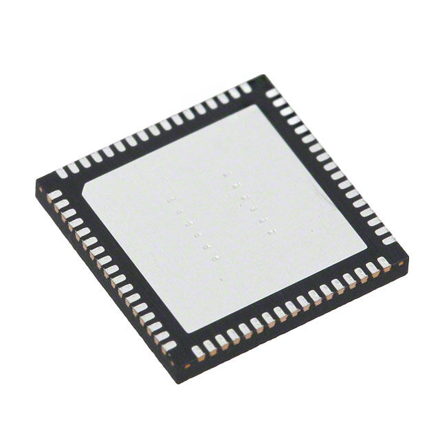
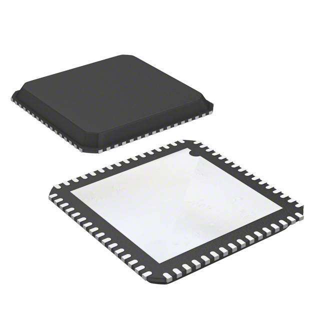
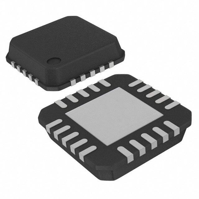
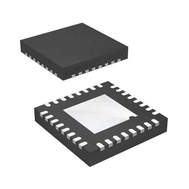
| 封装/外壳 | 40-VFQFN 裸露焊盘 |
| 封装/箱体 | QFN-40 |
| 工作温度 | -40°C ~ 125°C |
| 工作电源电压 | 2 V to 3.6 V |
| 工厂包装数量 | 1000 |
| 应用 | RF4CE |
| 接口类型 | 2-Wire, I2C, SPI |
| 数据RAM大小 | 8 kB |
| 数据Ram类型 | RAM |
| 数据ROM大小 | 4 kB |
| 数据Rom类型 | EEPROM |
| 数据总线宽度 | 32 bit |
| 数据接口 | PCB,表面贴装 |
| 数据速率(最大值) | - |
| 最大工作温度 | + 125 C |
| 最大时钟频率 | 32 MHz |
| 最小工作温度 | - 40 C |
| 标准包装 | 1 |
| 核心 | RISC |
| 灵敏度 | -95dBm |
| 片上ADC | Yes |
| 电压-电源 | 2 V ~ 3.6 V |
| 电流-传输 | 15mA |
| 电流-接收 | 17mA |
| 电源电压-最大 | 3.6 V |
| 电源电压-最小 | 2 V |
| 程序存储器大小 | 64 kB |
| 程序存储器类型 | Flash, EEPROM |
| 调制或协议 | 802.15.4 |
| 输入/输出端数量 | 20 I/O |
| 频率 | 2.4GHz |


- 商务部:美国ITC正式对集成电路等产品启动337调查
- 曝三星4nm工艺存在良率问题 高通将骁龙8 Gen1或转产台积电
- 太阳诱电将投资9.5亿元在常州建新厂生产MLCC 预计2023年完工
- 英特尔发布欧洲新工厂建设计划 深化IDM 2.0 战略
- 台积电先进制程称霸业界 有大客户加持明年业绩稳了
- 达到5530亿美元!SIA预计今年全球半导体销售额将创下新高
- 英特尔拟将自动驾驶子公司Mobileye上市 估值或超500亿美元
- 三星加码芯片和SET,合并消费电子和移动部门,撤换高东真等 CEO
- 三星电子宣布重大人事变动 还合并消费电子和移动部门
- 海关总署:前11个月进口集成电路产品价值2.52万亿元 增长14.8%


PDF Datasheet 数据手册内容提取
Data Sheet: JN516x IEEE802.15.4 Wireless Microcontroller Overview Features: Radio • 2.4GHz IEEE802.15.4 compliant The JN516x series is a range of ultra low power, high performance wireless • 128-bit AES security processor microcontrollers supporting JenNet-IP, ZigBee PRO or RF4CE networking stacks to facilitate the development of Home Automation, Smart Energy, • MAC accelerator with packet formatting, CRCs, address check, Light Link and Remote control applications. They feature an enhanced 32- auto-acks, timers bit RISC processor with embedded Flash and EEPROM memory, offering high coding efficiency through variable width instructions, a multi-stage • Integrated ultra low power sleep instruction pipeline and low power operation with programmable clock oscillator – 0.6µA speeds. They also include a 2.4GHz IEEE802.15.4 compliant transceiver • 2.0V to 3.6V battery operation and a comprehensive mix of analogue and digital peripherals. Three • Deep sleep current 0.12µA (Wake-up memory configurations are available to suit different applications. The best from IO) in class operating current of 15mA, with a 0.6uA sleep timer mode, gives • <$0.15 external component cost excellent battery life allowing operation direct from a coin cell. • RX current 17mA , TX 15mA The peripherals support a wide range of applications. They include a 2-wire • Receiver sensitivity -95dBm I2C, and SPI ports which can operate as either master or slave, a four • Transmit power 2.5dBm channel ADC with battery and a temperature sensor. It can support a large • Time of Flight engine for ranging switch matrix of up to 100 elements, or alternatively a 20 key capacitive touch pad. • Antenna Diversity (Auto RX) Features: Microcontroller Block Diagram • 32-bit RISC CPU, 1 to 32MHz clock speed WWTTaaiittmmcchheeddrroogg 8R/3A2MK 64/1F6l0a/s2h56K MasteSr P&I Slave • Variable instruction width for high 2-Wire Serial coding efficiency 2.4GHz Voltage Brownout (Master/Slave) • Multi-stage instruction pipeline Radio 32-bit 4xPWM + Timer Including O-QPSK RISC CPU • JN5161: 64kB/8kB/4kB Diversity Modem 2xUART • JN5164: 160kB/32kB/4kB 4kB 20 DIO • JN5168: 256kB/32kB/4kB EEPROM IEEE 802.15.4 Sleep Counter (Flash/RAM/EEPROM) XTAL PBraosceebsasnodr • Data EEPROM with guaranteed 100k 4-Channel write operations. 10-bit ADC Power 128-bit AES • RF4CE, JenNet-IP, ZigBee SE and Hardware Battery and Management Encryption Temp Sensors ZigBee Light Link stacks • 2-wire I2C compatible serial interface. Can operate as either master or slave • 5xPWM (4x timer & 1 timer/counter) • 2 low power sleep counters Benefits Applications • 2x UART • Single chip device to run • Robust and secure low power • SPI Master & Slave port, 3 selects stack and application wireless applications • Supply voltage monitor with 8 • Very low current solution for • RF4CE Remote Controls programmable thresholds long battery life – over 10 yrs • JenNet-IP networks • 4-input 10-bit ADC, comparator • Supports multiple network • ZigBee SE networks • Battery and temperature sensors stacks • Highly featured 32-bit RISC • ZigBee Light Link networks • Watchdog & Brown Out Reset CPU for high performance • Lighting & Home automation • Up to 20 Digital IO Pins (DIO) and low power • Toys and gaming peripherals • Infra-red remote control transmitter • System BOM is low in • Smart Energy component count and cost • Energy harvesting, for Temp range (-40°C to +125°C) • Flexible sensor interfacing example self powered light 6x6mm 40-lead options switch Lead-free and RoHS compliant © NXP Laboratories UK 2013 JN-DS-JN516x v1.3 Production 1
Contents Benefits 1 Applications 1 1 Introduction 6 1.1 Wireless Transceiver 6 1.2 RISC CPU and Memory 6 1.3 Peripherals 7 1.4 Block Diagram – JN516x 8 2 Pin Configurations 9 2.1 Pin Assignment 10 2.2 Pin Descriptions 12 2.2.1 Power Supplies 12 2.2.2 Reset 12 2.2.3 32MHz Oscillator 12 2.2.4 Radio 12 2.2.5 Analogue Peripherals 13 2.2.6 Digital Input/Output 13 3 CPU 15 4 Memory Organisation 16 4.1 FLASH 16 4.2 RAM 16 4.3 OTP Configuration Memory 16 4.4 EEPROM 17 4.5 External Memory 17 4.6 Peripherals 17 4.7 Unused Memory Addresses 17 5 System Clocks 18 5.1 High-Speed (32MHz) System Clock 18 5.1.1 32MHz Crystal Oscillator 18 5.1.2 High-Speed RC Oscillator 19 5.2 Low-speed (32kHz) System Clock 19 5.2.1 32kHz RC Oscillator 19 5.2.2 32kHz Crystal Oscillator 20 5.2.3 32kHz External Clock 20 6 Reset 21 6.1 Internal Power-On / Brown-out Reset (BOR) 21 6.2 External Reset 22 6.3 Software Reset 22 6.4 Supply Voltage Monitor (SVM) 22 6.5 Watchdog Timer 23 7 Interrupt System 24 7.1 System Calls 24 7.2 Processor Exceptions 24 7.2.1 Bus Error 24 2 JN-DS-JN516x v1.3 Production © NXP Laboratories UK 2013
7.2.2 Alignment 24 7.2.3 Illegal Instruction 24 7.2.4 Stack Overflow 24 7.3 Hardware Interrupts 25 8 Wireless Transceiver 26 8.1 Radio 26 8.1.1 Radio External Components 27 8.1.2 Antenna Diversity 27 8.2 Modem 29 8.3 Baseband Processor 30 8.3.1 Transmit 30 8.3.2 Reception 30 8.3.3 Auto Acknowledge 31 8.3.4 Beacon Generation 31 8.3.5 Security 31 8.4 Security Coprocessor 31 8.5 Time of Flight Engine 31 9 Digital Input/Output 32 10 Serial Peripheral Interface 34 10.1 Serial Peripheral Interface Master 34 10.2 Serial Peripheral Interface Slave 37 11 Timers 38 11.1 Peripheral Timer/Counters 38 11.1.1 Pulse Width Modulation Mode 39 11.1.2 Capture Mode 39 11.1.3 Counter/Timer Mode 40 11.1.4 Delta-Sigma Mode 40 11.1.5 Infra-Red Transmission Mode 41 11.1.6 Example Timer/Counter Application 41 11.2 Tick Timer 42 11.3 Wakeup Timers 42 11.3.1 32 KHZ RC Oscillator Calibration 43 12 Pulse Counters 44 13 Serial Communications 45 13.1 Interrupts 46 13.2 UART Application 46 14 JTAG Test Interface 48 2 15 Two-Wire Serial Interface (I C) 49 15.1 Connecting Devices 49 15.2 Clock Stretching 50 15.3 Master Two-wire Serial Interface 50 15.4 Slave Two-wire Serial Interface 52 16 Random Number Generator 53 © NXP Laboratories UK 2013 JN-DS-JN516x v1.3 Production 3
17 Analogue Peripherals 54 17.1 Analogue to Digital Converter 54 17.1.1 Operation 55 17.1.2 Supply Monitor 56 17.1.3 Temperature Sensor 56 17.1.4 ADC Sample Buffer Mode 56 17.2 Comparator 56 18 Power Management and Sleep Modes 57 18.1 Operating Modes 57 18.1.1 Power Domains 57 18.2 Active Processing Mode 57 18.2.1 CPU Doze 57 18.3 Sleep Mode 57 18.3.1 Wakeup Timer Event 58 18.3.2 DIO Event 58 18.3.3 Comparator Event 58 18.3.4 Pulse Counter 58 18.4 Deep Sleep Mode 58 19 Electrical Characteristics 59 19.1 Maximum Ratings 59 19.2 DC Electrical Characteristics 59 19.2.1 Operating Conditions 59 19.2.2 DC Current Consumption 60 19.2.3 I/O Characteristics 61 19.3 AC Characteristics 61 19.3.1 Reset and Supply Voltage Monitor 61 19.3.2 SPI Master Timing 63 19.3.3 SPI Slave Timing 64 19.3.4 Two-wire Serial Interface 65 19.3.5 Wakeup Timings 65 19.3.6 Bandgap Reference 66 19.3.7 Analogue to Digital Converters 66 19.3.8 Comparator 67 19.3.9 32kHz RC Oscillator 67 19.3.10 32kHz Crystal Oscillator 68 19.3.11 32MHz Crystal Oscillator 68 19.3.12 High-Speed RC Oscillator 69 19.3.13 Temperature Sensor 69 19.3.14 Non-Volatile Memory 69 19.3.15 Radio Transceiver 70 Appendix A Mechanical and Ordering Information 76 A.1 SOT618-1 HVQFN40 40-pin QFN Package Drawing 76 A.2 Footprint Information 77 A.3 Ordering Information 78 A.4 Device Package Marking 79 A.5 Tape and Reel Information 80 A.5.1 Tape Orientation and Dimensions 80 A.5.2 Reel Information: 180mm Reel 81 A.5.3 Reel Information: 330mm Reel 82 4 JN-DS-JN516x v1.3 Production © NXP Laboratories UK 2013
A.5.4 Dry Pack Requirement for Moisture Sensitive Material 82 Appendix B Development Support 83 B.1 Crystal Oscillators 83 B.1.1 Crystal Equivalent Circuit 83 B.1.2 Crystal Load Capacitance 83 B.1.3 Crystal ESR and Required Transconductance 84 B.2 32MHz Oscillator 85 B.3 32kHz Oscillator 87 B.4 JN516x Module Reference Designs 89 B.4.1 Schematic Diagram 89 B.4.2 PCB Design and Reflow Profile 91 B.4.3 Moisture Sensitivity Level (MSL) 91 Related Documents 92 RoHS Compliance 92 Status Information 92 Disclaimers 93 Trademarks 93 Version Control 93 Contact Details 94 © NXP Laboratories UK 2013 JN-DS-JN516x v1.3 Production 5
1 Introduction The JN516x is an IEEE802.15.4 wireless microcontroller that provides a fully integrated solution for applications using the IEEE802.15.4 standard in the 2.4 - 2.5GHz ISM frequency band [1], including Zigbee PRO, ZigBee Smart Energy, ZigBee LightLink, RF4CE and JenNet-IP. There are 3 versions in the range, differing only by memory configuration JN5161-001: 64kB Flash, 8kB RAM, 4 kB EEPROM, suitable for IEEE802.15.4 and RF4CE applications JN5164-001: 160kB Flash, 32kB RAM, 4 kB EEPROM suitable for Jennet-IP, IEEE802.15.4 and RF4CE applications JN5168-001: 256kB Flash, 32kB RAM, 4 kB EEPROM suitable for all applications Applications that transfer data wirelessly tend to be more complex than wired ones. Wireless protocols make stringent demands on frequencies, data formats, timing of data transfers, security and other issues. Application development must consider the requirements of the wireless network in addition to the product functionality and user interfaces. To minimise this complexity, NXP provides a series of software libraries and interfaces that control the transceiver and peripherals of the JN516x. These libraries and interfaces remove the need for the developer to understand wireless protocols and greatly simplifies the programming complexities of power modes, interrupts and hardware functionality. In view of the above, it is not necessary to provide the register details of the JN516x in the datasheet. The device includes a Wireless Transceiver, RISC CPU, on chip memory and an extensive range of peripherals. 1.1 Wireless Transceiver The Wireless Transceiver comprises a 2.45GHz radio, a modem, a baseband controller and a security coprocessor. In addition, the radio also provides an output to control transmit-receive switching of external devices such as power amplifiers allowing applications that require increased transmit power to be realised very easily. Appendix B.4, describes a complete reference design including Printed Circuit Board (PCB) design and Bill Of Materials (BOM). The security coprocessor provides hardware-based 128-bit AES-CCM* modes as specified by the IEEE802.15.4 2006 standard. Specifically this includes encryption and authentication covered by the MIC –32/-64/-128, ENC and ENC-MIC –32/-64/-128 modes of operation. The transceiver elements (radio, modem and baseband) work together to provide IEEE802.15.4 (2006) MAC and PHY functionality under the control of a protocol stack. Applications incorporating IEEE802.15.4 functionality can be developed rapidly by combining user-developed application software with a protocol stack library. 1.2 RISC CPU and Memory A 32-bit RISC CPU allows software to be run on-chip, its processing power being shared between the IEEE802.15.4 MAC protocol, other higher layer protocols and the user application. The JN516x has a unified memory architecture, code memory, data memory, peripheral devices and I/O ports are organised within the same linear address space. The device contains up to 256kbytes of Flash, up to 32kbytes of RAM and 4kbytes EEPROM . 6 JN-DS-JN516x v1.3 Production © NXP Laboratories UK 2013
1.3 Peripherals The following peripherals are available on chip: • Master SPI port with three select outputs • Slave SPI port • Two UART’s, one capable of hardware flow control (4-wire, includes RTS/CTS), and the other just 2-wire (RX/TX) • One programmable Timer/Counter which supports Pulse Width Modulation (PWM) and capture/compare, plus four PWM timers which support PWM and Timer modes only. • Two programmable Sleep Timers and a Tick Timer • Two-wire serial interface (compatible with SMbus and I2C) supporting master and slave operation • Twenty digital I/O lines (multiplexed with peripherals such as timers, SPI and UARTs) • Two digital outputs (multiplexed with SPI port) • 10-bit, Analogue to Digital converter with up to four input channels. Autonomous multi-channel sampling • Programmable analogue comparator • Internal temperature sensor and battery monitor • Two low power pulse counters • Random number generator • Watchdog Timer and Supply Voltage Monitor • JTAG hardware debug port • Infra-red remote control transmitter, supported by one of the PWM timers • Transmit and receive antenna diversity with automatic receive switching based on received energy detection • Time of Flight engine for ranging User applications access the peripherals using the Integrated Peripherals API. This allows applications to use a tested and easily understood view of the peripherals allowing rapid system development. © NXP Laboratories UK 2013 JN-DS-JN516x v1.3 Production 7
1.4 Block Diagram – JN516x SPICLK SPIMOSI SPI Slave SPIMISO SPISEL0 Tick Timer DIO0 SPICLK ProIgnrtaemrrumpat b le 32-bit RISC CPU SPI SSPPIIMMOISSOI DIO1 Controller Master SPISEL0 DIO2 SPISEL1 SPISEL2 DIO3 From Peripherals DIO4 TXD0 RXD0 DIO5 UART0 RTS0 CTS0 DIO6 RA M FLASH EEPROM TxD1 DIO7 32/32/8 KB 256/ 160/64KB 4KB UART1 RxD1 DIO8 CPU and 16MHz TIM0CK_GT DIO9 System Clock Timer0 TIM0OUT MUX TIM0CAP DIO10 VB_XX VDD1 Voltage 1.8V PPWWMM12 DIO11 VDD2 Regulators PWMs PWM3 DIO12 XTXATLA_LO_UINT 3G2eMCnHleozrca kXt otarl SSoCRuelaorlectceeck t & spHeOeigsdhc R- C In2te-wrfiarec e SPSIFWI_FCM_DL4K DDIIOO1134 RESETN Reset Watchdog Pulse PC0 DIO15 Timer Counters PC1 DIO16 Wakeup Time r0 JTAG_TDI Supply Volta ge JTAG JTAG_TMS Monit or Debug JTAG_TCK DIO17 WTiamkeeru1p JTAG_TDO DIO18 Antenna ADO DIO19 32kSHezl eCcltoc k 32KIN Diversity A DE DO0 Wireless 32RkCH z 32XktaHl z 3322KKXXTTAALLION UT Transceive r DO1 Osc Osc Security Processor Supply Monitor VREF/AAADDDCCC132 MU ADC Dig ital Baseband ADC4 X Temperatu re RF_IN Sensor Radio VCOTUNE IBIAS COMP1M Comparator1 COMP1P Figure 1: JN516x Block Diagram 8 JN-DS-JN516x v1.3 Production © NXP Laboratories UK 2013
2 Pin Configurations DIO15 VSS2 DIO14 DIO13 DIO12 VB_DIG DIO11 DIO10 DIO9 DIO8 40 39 38 37 36 35 34 33 32 31 DIO16 1 30 VDD2 DIO1 7 2 29 DIO7 RESETN 3 28 DIO6 XTAL_OUT 4 27 DIO5 VSSA XTAL_IN 5 26 DIO4 VB_SYNTH 6 25 VB_RAM VCOTUNE 7 24 DIO19 VB_VCO 8 23 DIO18 VDD1 9 22 DO1 IBIAS 10 21 VSS1 11 12 13 14 15 16 17 18 19 20 EF/ADC2 VB_RF2 RF_IN VB_RF1 ADC1 DIO0 DIO1 DIO2 DIO3 DO0 R V Figure 2: 40-pin QFN Configuration (top view) Note: Please refer to Appendix B.4 JN516x Module Reference Design for important applications information regarding the connection of the PADDLE to the PCB. © NXP Laboratories UK 2013 JN-DS-JN516x v1.3 Production 9
2.1 Pin Assignment Pin No Power supplies Signal Description Type 6, 8, VB_SYNTH, VB_VCO, VB_RF2, VB_RF1, VB_RAM, VB_DIG 1.8V Regulated supply voltage 12, 14, 25, 35 9, 30 VDD1, VDD2 3.3V Supplies: VDD1 for analogue, VDD2 for digital 21, 39, VSS1, VSS2, VSSA 0V Grounds (see appendix A.2 Paddle for paddle details) General 3 RESETN CMOS Reset input 4,5 XTAL_OUT, XTAL_IN 1.8V System crystal oscillator Radio 7 VCOTUNE 1.8V VCO tuning RC network 10 IBIAS 1.8V Bias current control 13 RF_IN 1.8V RF antenna Analogue Peripheral I/O 15, 16, ADC1, DIO0 (ADC3), DIO1 (ADC4) 3.3V ADC inputs 17 11 VREF/ADC2 1.8V Analogue peripheral reference voltage or ADC input 2 1, 2 DIO16 (COMP1P), DIO17 (COMP1M) 3.3V Comparator inputs Digital Peripheral I/O Primary Alternate Functions 16 DIO0 SPISEL1 ADC3 CMOS DIO0, SPI Master Select Output 1 or ADC input 3 17 DIO1 SPISEL2 ADC4 PC0 CMOS DIO1, SPI Master Select Output 2, ADC input 4 or Pulse Counter 0 Input 18 DIO2 RFRX TIM0CK_GT CMOS DIO2, Radio Receive Control Output or Timer0 Clock/Gate Input 19 DIO3 RFTX TIM0CAP CMOS DIO3, Radio Transmit Control Output or Timer0 Capture Input 26 DIO4 CTS0 JTAG_TCK TIM0OUT PC0 CMOS DIO4, UART 0 Clear To Send Input, JTAG CLK Input, Timer0 PWM Output, or Pulse Counter 0 input 27 DIO5 RTS0 JTAG_TMS PWM1 PC1 CMOS DIO5, UART 0 Request To Send Output, JTAG Mode Select Input, PWM1 Output or Pulse Counter 1 Input 28 DIO6 TXD0 JTAG_TDO PWM2 CMOS DIO6, UART 0 Transmit Data Output, JTAG Data Output or PWM2 Output 29 DIO7 RXD0 JTAG_TDI PWM3 CMOS DIO7, UART 0 Receive Data Input, JTAG Data Input or PWM 3 Output 31 DIO8 TIM0CK_GT PC1 PWM4 CMOS DIO8, Timer0 Clock/Gate Input, Pulse Counter1 Input or PWM 4 Output 10 JN-DS-JN516x v1.3 Production © NXP Laboratories UK 2013
32 DIO9 TIM0CAP 32KXTALIN RXD1 32KIN CMOS DIO9, Timer0 Capture Input, 32K External Crystal Input, UART 1 Receive Data Input or 32K external clock Input 33 DIO10 TIM0OUT 32KXTALOUT CMOS DIO10, Timer0 PWM Output or 32K External Crystal Output 34 DIO11 PWM1 TXD1 CMOS DIO11, PWM1 Output or UART 1 Transmit Data Output 36 DIO12 PWM2 CTS0 JTAG_TCK ADO SPISMO CMOS DIO12, PWM2 Output, UART SI 0 Clear To Send Input, JTAG CLK Input, Antenna Diversity Odd Output or SPI Slave Master Out Slave In Input 37 DIO13 PWM3 RTS0 JTAG_TMS ADE SPISMI CMOS DIO13, PWM3 Output, UART SO 0 Request To Send Output, JTAG Mode Select Input, Antenna Diversity Even output or SPI Slave Master In Slave Out Output 38 DIO14 SIF_CLK TXD0 TXD1 JTAG_TDO SPISEL SPISSE CMOS DIO14, Serial Interface 1 L Clock, UART 0 Transmit Data Output, UART 1 Transmit Data Output, JTAG Data Output, SPI Master Select Output 1 or SPI Slave Select Input 40 DIO15 SIF_D RXD0 RXD1 JTAG_TDI SPISEL SPISCL CMOS DIO15, Serial Interface Data, 2 K UART 0 Receive Data Input, UART 1 Receive Data Input, JTAG Data Input, SPI Master Select Output 2 or SPI Slave Clock Input 1 DIO16 COMP1P SIF_CLK SPISMOSI CMOS DIO16, Comparator Positive Input, Serial Interface clock or SPI Slave Master Out Slave In Input 2 DIO17 COMP1M SIF_D SPISMISO CMOS DIO17, Comparator Negative Input, Serial Interface Data or SPI Slave Master In Slave Out Output 23 DIO18 SPIMOSI CMOS SPI Master Out Slave In Output 24 DIO19 SPISEL0 CMOS SPI Master Select Output 0 20 DO0 SPICLK PWM2 CMOS SPI Master Clock Output or PWM2 Output 22 DO1 SPIMISO PWM3 CMOS SPI Master In Slave Out Input or PWM3 Output The PCB schematic and layout rules detailed in Appendix B.4 must be followed. Failure to do so will likely result in the JN516x failing to meet the performance specification detailed herein and worst case may result in device not functioning in the end application. © NXP Laboratories UK 2013 JN-DS-JN516x v1.3 Production 11
2.2 Pin Descriptions 2.2.1 Power Supplies The device is powered from the VDD1 and VDD2 pins, each being decoupled with a 100nF ceramic capacitor. VDD1 is the power supply to the analogue circuitry; it should be decoupled to ground. VDD2 is the power supply for the digital circuitry; and should also be decoupled to ground. In addition, a common 10µF tantalum capacitor is required for low frequencies. Decoupling pins for the internal 1.8V regulators are provided which each require a100nF capacitor located as close to the device as practical. VB_SYNTH, VB_RAM and VB_DIG require only a 100nF capacitor. VB_RF and VB_RF2 should be connected together as close to the device as practical, and require one 100nF capacitor and one 47pF capacitor. The pin VB_VCO requires a 10nF capacitor. Refer to B.4.1 for schematic diagram. VSSA (paddle), VSS1, VSS2 are the ground pins. Users are strongly discouraged from connecting their own circuits to the 1.8v regulated supply pins, as the regulators have been optimised to supply only enough current for the internal circuits. 2.2.2 Reset RESETN is an active low reset input pin that is connected to a 500kΩ internal pull-up resistor. It may be pulled low by an external circuit. Refer to Section 6.2 for more details. 2.2.3 32MHz Oscillator A crystal is connected between XTAL_IN and XTAL_OUT to form the reference oscillator, which drives the system clock. A capacitor to analogue ground is required on each of these pins. Refer to Section 5.1 for more details. The 32MHz reference frequency is divided down to 16MHz and this is used as the system clock throughout the device. 2.2.4 Radio The radio is a single ended design, requiring a capacitor and just two inductors to match to 50Ω microstrip line to the RF_IN pin. An external resistor (43kΩ) is required between IBIAS and analogue ground (paddle) to set various bias currents and references within the radio. 12 JN-DS-JN516x v1.3 Production © NXP Laboratories UK 2013
2.2.5 Analogue Peripherals The ADC requires a reference voltage to use as part of its operation. It can use either an internal reference voltage or an external reference connected to VREF. This voltage is referenced to analogue ground and the performance of the analogue peripherals is dependent on the quality of this reference. There are four ADC inputs and a pair of comparator inputs. ADC1 has a designated input pin but ADC2 uses the same pin as VREF, invalidating its use as an ADC pin when an external reference voltage is required. The remaining 2 ADC channels are shared with the digital I/Os DIO0 and DIO1 and connect to pins 16 and 17. When these two ADC channels are selected, the corresponding DIOs must be configured as Inputs with their pull-ups disabled. Similarly, the comparator shares pins 1 and 2 with DIO16 and DIO17, so when the comparator is selected these pins must be configured as Inputs with their pull-ups disabled. The analogue I/O pins on the JN516x can have signals applied up to 0.3v higher than VDD1. A schematic view of the analogue I/O cell is shown in Figure 3. Figure 4 demonstrates a special case, where a digital I/O pin doubles as an input to analogue devices. This applies to ADC3, ADC4, COMP1P and COMP1M. In reset, sleep and deep sleep, the analogue peripherals are all off. In sleep, the comparator may optionally be used as a wakeup source. Unused ADC and comparator inputs should not be left unconnected, for example connected to analogue ground. VDD1 Analogue I/O Pin Analogue Peripheral VSSA Figure 3: Analogue I/O Cell 2.2.6 Digital Input/Output For the DC properties of these pins see Section 19.2.3. When used in their primary function all Digital Input/Output pins are bi-directional and are connected to weak internal pull up resistors (50kΩ nominal) that can be disabled. When used in their secondary function (selected when the appropriate peripheral block is enabled through software library calls), their direction is fixed by the function. The pull up resistor is enabled or disabled independently of the function and direction; the default state from reset is enabled. A schematic view of the digital I/O cell is in Figure 4. The dotted lines through resistor RESD represent a path that exists only on DIO0, DIO1, DIO16 and DIO17 which are also inputs to the ADC (ADC3, ADC4) and Comparator (COMP1P, COMP1M) respectively. To use these DIO pins for their analogue functions, the DIO must be set as an Input with its pull-up resistor, RPU, disabled. © NXP Laboratories UK 2013 JN-DS-JN516x v1.3 Production 13
VDD2 ADC or Pu COMP1 Input IE RPU RESD RPROT I DIO[x] Pin VSS VSS O OE Figure 4: DIO Pin Equivalent Schematic In reset, the digital peripherals are all off and the DIO pins are set as high-impedance inputs. During sleep and deep sleep, the DIO pins retain both their input/output state and output level that was set as sleep commences. If the DIO pins were enabled as inputs and the interrupts were enabled then these pins may be used to wake up the JN516x from sleep. 14 JN-DS-JN516x v1.3 Production © NXP Laboratories UK 2013
3 CPU The CPU of the JN516x is a 32-bit load and store RISC processor. It has been architected for three key requirements: • Low power consumption for battery powered applications • High performance to implement a wireless protocol at the same time as complex applications • Efficient coding of high-level languages such as C provided with the Software Developers Kit It features a linear 32-bit logical address space with unified memory architecture, accessing both code and data in the same address space. Registers for peripheral units, such as the timers, UART and the baseband processor are also mapped into this space. The CPU has access to a block of 15 32-bit General-Purpose (GP) registers together with a small number of special purpose registers which are used to store processor state and control interrupt handling. The contents of any GP register can be loaded from or stored to memory, while arithmetic and logical operations, shift and rotate operations, and signed and unsigned comparisons can be performed either between two registers and stored in a third, or between registers and a constant carried in the instruction. Operations between general or special-purpose registers execute in one cycle while those that access memory require a further cycle to allow the memory to respond. The instruction set manipulates 8, 16 and 32-bit data; this means that programs can use objects of these sizes very efficiently. Manipulation of 32-bit quantities is particularly useful for protocols and high-end applications allowing algorithms to be implemented in fewer instructions than on smaller word-size processors, and to execute in fewer clock cycles. In addition, the CPU supports hardware Multiply that can be used to efficiently implement algorithms needed by Digital Signal Processing applications. The instruction set is designed for the efficient implementation of high-level languages such as C. Access to fields in complex data structures is very efficient due to the provision of several addressing modes, together with the ability to be able to use any of the GP registers to contain the address of objects. Subroutine parameter passing is also made more efficient by using GP registers rather than pushing objects onto the stack. The recommended programming method for the JN516x is by using C, which is supported by a software developer kit comprising a C compiler, linker and debugger. The CPU architecture also contains features that make the processor suitable for embedded, real-time applications. In some applications, it may be necessary to use a real-time operating system to allow multiple tasks to run on the processor. To provide protection for device-wide resources being altered by one task and affecting another, the processor can run in either supervisor or user mode, the former allowing access to all processor registers, while the latter only allows the GP registers to be manipulated. Supervisor mode is entered on reset or interrupt; tasks starting up would normally run in user mode in a RTOS environment. Embedded applications require efficient handling of external hardware events. Exception processing (including reset and interrupt handling) is enhanced by the inclusion of a number of special-purpose registers into which the PC and status register contents are copied as part of the operation of the exception hardware. This means that the essential registers for exception handling are stored in one cycle, rather than the slower method of pushing them onto the processor stack. The PC is also loaded with the vector address for the exception that occurred, allowing the handler to start executing in the next cycle. To improve power consumption a number of power-saving modes are implemented in the JN516x, described more fully in Section 18. One of these modes is the CPU doze mode; under software control, the processor can be shut down and on an interrupt it will wake up to service the request. Additionally, it is possible under software control, to set the speed of the CPU to 1, 2, 4, 8, 16 or 32MHz. This feature can be used to trade-off processing power against current consumption. © NXP Laboratories UK 2013 JN-DS-JN516x v1.3 Production 15
4 Memory Organisation This section describes the different memories found within the JN516x. The device contains Flash, RAM, and EEPROM memory, the wireless transceiver and peripherals all within the same linear address space. 0xFFFFFFFF Unpopulated 0xF0008000 RAM 0x04000000 Peripherals 0x02000000 Flash & EEPROM Registers 0x01000000 0x000C0000 FLASH Applications Code (256KB) 0x00080000 FLASH Boot Code 8K 0x00000000 Figure 5: JN5168 Memory Map 4.1 FLASH The embedded Flash consists of 2 parts: an 8K region used for holding boot code, and a 256K region (JN5168) used for application code. The sector size of the application code is always 32K, for any size of Flash memory. The maximum number of write cycles or endurance is, 10k guaranteed and typically 100k, while the data retention is guaranteed for at least 10 years. The boot code region is pre-programmed by NXP on supplied parts, and contains code to handle reset, interrupts and other events (see section 7). It also contains a Flash Programming Interface to allow interaction with the PC-based Flash Programming Utility which allows user code compiled using the supplied SDK to be programmed into the Application space. For further information, refer to the Flash Programmer User Guide.[9]. The memory can be erased by a single or multiple sectors and written to in units of 256 bytes, known as pagewords. 4.2 RAM The JN516x devices contain up to 32Kbytes of high speed RAM, which can be accessed by the CPU in a single clock cycle. It is primarily used to hold the CPU Stack together with program variables and data. If necessary, the CPU can execute code contained within the RAM (although it would normally just execute code directly from the embedded Flash). Software can control the power supply to the RAM allowing the contents to be maintained during a sleep period when other parts of the device are un-powered, allowing a quicker resumption of processing once woken. 4.3 OTP Configuration Memory The JN516x devices contain a quantity of One Time Programmable (OTP) memory as part of the embedded Flash (Index Sector). This can be used to securely hold such things as a user 64-bit MAC address and a 128-bit AES security key. By default the 64-bit MAC address is pre-programmed by NXP on supplied parts; however customers 16 JN-DS-JN516x v1.3 Production © NXP Laboratories UK 2013
can use their own MAC address and override the default one. The user MAC address and other data can be written to the OTP memory using the Flash programmer [9]. Details on how to obtain and install MAC addresses can be found in the Flash Programmer User Guide. In addition 384bits are available, organised as three 128bit words, for customer use for storage of configuration or other information. 4.4 EEPROM The JN516x devices contain 4Kbytes of EEPROM. The maximum number of write cycles or endurance is, 100k guaranteed and 1M typically while the data retention is guaranteed for at least 20 years. (The Persistent Data Manager, includes a wear-levelling algorithm which can help to extend the endurance.) This non-volatile memory is primarily used to hold persistent data generated from such things as the Network Stack software component (e.g. network topology, routing tables). As the EEPROM holds its contents through sleep and reset events, this means more stable operation and faster recovery is possible after outages. Access to the EEPROM is via registers mapped into the Flash and EEPROM Registers region of the address map. The memory can be erased by a single or multiple pages of 64 bytes. It can be written to in single or multiple bytes up to 64 bytes. The customer may use part of the EEPROM to store its own data if desired by interfacing with the Persistent Data Manager. Optionally the PDM can also store data in an external memory. For further information, please read - JenOS User Guide [12]. 4.5 External Memory An optional external serial non-volatile memory (eg Flash or EEPROM) with a SPI interface may be used to provide additional storage for program code, such as a new code image or further data for the device when external power is removed. The memory can be connected to the SPI Master interface using select line SPISEL0 (see fig 6 for details) Serial JN516x Memory SPISEL0 SS SPIMISO SDO SPIMOSI SDI SPICLK CLK Figure 6: Connecting External Serial Memory The contents of the external serial memory may be encrypted. The AES security processor combined with a user programmable 128-bit encryption key is used to encrypt the contents of the external memory. The encryption key is stored in the flash memory index section. When bootloading program code from external serial memory, the JN516x automatically accesses the encryption key to execute the decryption process, user program code does not need to handle any of the decryption process; it is transparent. For more details, including the how the program code encrypts data for the external memory, see the application note Boot Loader Operation. [8] 4.6 Peripherals All peripherals have their registers mapped into the memory space. Access to these registers requires 3 peripheral clock cycles. Applications have access to the peripherals through the software libraries that present a high-level view of the peripheral’s functions through a series of dedicated software routines. These routines provide both a tested method for using the peripherals and allow bug-free application code to be developed more rapidly. For details, see Peripherals API User Guide [4]. 4.7 Unused Memory Addresses Any attempt to access an unpopulated memory area will result in a bus error exception (interrupt) being generated. © NXP Laboratories UK 2013 JN-DS-JN516x v1.3 Production 17
5 System Clocks Two system clocks are used to drive the on-chip subsystems of the JN516x. The wake-up timers are driven from a low frequency clock (notionally 32kHz). All other subsystems (transceiver, processor, memory and digital and analogue peripherals) are driven by a high-speed clock (notionally 32MHz), or a divided-down version of it. The high-speed clock is either generated by the accurate crystal-controlled oscillator (32MHz) or the less accurate high-speed RC oscillator ( 27-32MHz calibrated). The low-speed clock is either generated by the accurate crystal- controlled oscillator (32.768kHz), the less accurate RC oscillator (centered on 32kHz) or can be supplied externally 5.1 High-Speed (32MHz) System Clock The selected high-speed system clock is used directly by the radio subsystem, whereas a divided-by-two version is used by the remainder of the transceiver and the digital and analogue peripherals. The direct or divided down version of the clock is used to drive the processor and memories (32, 16, 8, 4, 2 or 1MHz). PERIPHERAL SYSTEM CLOCK 32MHz Crystal Div by 2 Oscillator High Speed CPU CLOCK Div by 1,2,4,8,16 or 32 RC Oscillator Figure 7 System and CPU Clocks Crystal oscillators are generally slow to start. Hence to provide a fast start-up following a sleep cycle or reset, the fast RC oscillator is always used as the initial source for the high-speed system clock. The oscillator starts very quickly and will run at 25-32MHz (uncalibrated) or 32MHz +/-5% (calibrated). Although this means that the system clock will be running at an undefined frequency (slightly slower or faster than nominal), this does not prevent the CPU and Memory subsystems operating normally, so the program code can execute. However, it is not possible to use the radio or UARTs, as even after calibration (initiated by the user software calling an API function) there is still a +/-5% tolerance in the clock rate over voltage and temperature. Other digital peripherals can be used (eg SPI Master/Slave), but care must be taken if using Timers due to the clock frequency inaccuracy. Further details of the High-Speed RC Oscillator can be found in section 19.3.11. On wake-up from sleep, the JN516x uses the Fast RC oscillator. It can then either: • Automatically switch over to use the 32MHz clock source when it has started up. • Continue to use the fast RC oscillator until software triggers the switch-over to the 32MHz clock source, for example when the radio is required. • Continue to use the RC oscillator until the device goes back into one of the sleep modes. The use of the fast RC Oscillator at wake-up means there is no need to wait for the 32MHz crystal oscillator to stabilise Consequently, the application code will start executing quickly using the clock from the high-speed RC oscillator. 5.1.1 32MHz Crystal Oscillator The JN516x contains the necessary on chip components to build a 32MHz reference oscillator with the addition of an external crystal resonator and two tuning capacitors. The schematic of these components are shown in Figure 8. The two capacitors, C1 and C2, should typically be 15pF and use a COG dielectric. Due to the small size of these capacitors, it is important to keep the traces to the external components as short as possible. The on chip transconductance amplifier is compensated for temperature variation, and is self-biasing by means of the internal resistor R1. This oscillator provides the frequency reference for the radio and therefore it is essential that the reference PCB layout and BOM are carefully followed. The electrical specification of the oscillator can be found in 18 JN-DS-JN516x v1.3 Production © NXP Laboratories UK 2013
Section 19.3.11. Please refer to Appendix B for development support with the crystal oscillator circuit. The oscillator includes a function which flags when the amplitude of oscillation has reached a satisfactory level for full operation, and this is checked before the source of the high-speed system clock is changed to the 32MHz crystal oscillator JN516x XTALIN R1 XTALOUT C1 C2 Figure 8: 32MHz Crystal Oscillator Connections For operation over the extended temperature range, 85 to 125 deg C, special care is required; this is because the temperature characteristics of crystal resonators are generally in excess of +/-40ppm frequency tolerance defined by the IEEE802.15.4 standard. The oscillator cell contains additional circuitry to compensate for the poor performance of the crystal resonators above 100 deg C. Full details, including the software API function, can be found in the application note JN516x Temperature-dependent Operating Guidelines [2] 5.1.2 High-Speed RC Oscillator An on-chip High-Speed RC oscillator is provided in addition to the 32MHz crystal oscillator for two purposes, to allow a fast start-up from reset or sleep and to provide a lower current alternative to the crystal oscillator for non-timing critical applications. By default the oscillator will run at 27MHz typically with a wide tolerance. It can be calibrated, using a software API function, which will result in a nominal frequency of 32MHz with a +/-1.6% tolerance at 3v and 25 deg C. However, it should be noted that over the full operating range of voltage and temperature this will increase to +/-5%. The calibration information is retained through speed cycles and when the oscillator is disabled, so typically the calibration function only needs to be called once. No external components are required for this oscillator. The electrical specification of the oscillator can be found in Section 19.3.12. 5.2 Low-speed (32kHz) System Clock The 32kHz system clock is used for timing the length of a sleep period (see Section 18). The clock can be selected from one of three sources through the application software: • 32kHz RC Oscillator • 32kHz Crystal Oscillator • 32kHz External Clock Upon a chip reset or power-up the JN516x defaults to using the internal 32kHz RC Oscillator. If another clock source is selected then it will remain in use for all 32kHz timing until a chip reset is performed. 5.2.1 32kHz RC Oscillator The internal 32kHz RC oscillator requires no external components. The internal timing components of the oscillator have a wide tolerance due to manufacturing process variation and so the oscillator runs nominally at 32kHz -10% /+40%. To make this useful as a timing source for accurate wakeup from sleep, a frequency calibration factor derived from the more accurate 16MHz clock may be applied. The calibration factor is derived through software, details can be found in Section 11.3.1. Software must check that the 32kHz RC oscillator is running before using it. The oscillator has a default current consumption of around 0.5uA, optionally this can be reduced to 0.375uA, however, the © NXP Laboratories UK 2013 JN-DS-JN516x v1.3 Production 19
calibrated accuracy and temperature coefficient will be worse as a consequence. For detailed electrical specifications, see Section 19.3.9. 5.2.2 32kHz Crystal Oscillator In order to obtain more accurate sleep periods, the JN516x contains the necessary on-chip components to build a 32kHz oscillator with the addition of an external 32.768kHz crystal and two tuning capacitors. The crystal should be connected between 32KXTALIN and 32KXTALOUT (DIO9 and DIO10), with two equal capacitors to ground, one on each pin. Due to the small size of the capacitors, it is important to keep the traces to the external components as short as possible. The electrical specification of the oscillator can be found in Section 19.3.10. The oscillator cell is flexible and can operate with a range of commonly available 32.768kHz crystals with load capacitances from 6 to 12.5pF. However, the maximum ESR of the crystal and the supply current are both functions of the actual crystal used, see Appendix B.1 for more details. JN516x 32KXTALIN 32KXTALOUT Figure 9: 32kHz Crystal Oscillator Connections 5.2.3 32kHz External Clock An externally supplied 32kHz reference clock on the 32KXTALIN input (DIO9) may be provided to the JN516x. This would allow the 32kHz system clock to be sourced from a very stable external oscillator module, allowing more accurate sleep cycle timings compared to the internal RC oscillator. (See Section 19.2.3) 20 JN-DS-JN516x v1.3 Production © NXP Laboratories UK 2013
6 Reset A system reset initialises the device to a pre-defined state and forces the CPU to start program execution from the reset vector. The reset process that the JN516x goes through is as follows. When power is first applied or when the external reset is released, the High-Speed RC oscillator and 32MHz crystal oscillator are activated. After a short wait period (13µsec approx) while the High-Speed RC starts up, and so long as the supply voltage satisfies the default Supply Voltage Monitor (SVM) threshold (2.0V+0.045V hysteresis), the internal 1.8V regulators are turned on to power the processor and peripheral logic. The regulators are allowed to stabilise (about 15us) followed by a further wait (150usec approx) to allow the Flash and EEPROM bandgaps to stabilise and allow their initialisation, including reading the user SVM threshold from the Flash. This is applied to the SVM and, after a brief pause (approx 2.5usec), the SVM is checked again. If the supply is above the new SVM threshold, the CPU and peripheral logic is released from reset and the CPU starts to run code beginning at the reset vector. This runs the bootloader code contained within the flash, which looks for a valid application to run, first from the internal flash and then from any connected external serial memory over the SPI Master interface. Once found, required variables are initialised in RAM before the application is called at its AppColdStart entry point. More details on the bootloader can be found in the application note - Boot Loader Operation. [8] The JN516x has five sources of reset: • Internal Power-on / Brown-out Reset (BOR) • External Reset • Software Reset • Watchdog timer • Supply Voltage detect Note: When the device exits a reset condition, device operating parameters (voltage, frequency, temperature, etc.) must be met to ensure operation. If these conditions are not met, then the device must be held in reset until the operating conditions are met. (See Section 19.3) 6.1 Internal Power-On / Brown-out Reset (BOR) For the majority of applications the internal power-on reset is capable of generating the required reset signal. When power is applied to the device, the power-on reset circuit monitors the rise of the VDD supply. When the VDD reaches the specified threshold, the reset signal is generated. This signal is held internally until the power supply and oscillator stabilisation time has elapsed, when the internal reset signal is then removed and the CPU is allowed to run. The BOR circuit has the ability to reject spikes on the VDD rail to avoid false triggering of the reset module. Typically for a negative going square pulse of duration 1uS, the voltage must fall to 1.2v before a reset is generated. Similarly for a triangular wave pulse of 10us width, the voltage must fall to 1.3v before causing a reset. The exact characteristics are complex and these are only examples. VDD Internal RESET Figure 10: Internal Power-on Reset When the supply drops below the pow er on reset ‘falling’ threshold, it will re-trigger the reset. If necessary, use of the external reset circuit show in Figure 11 is suggested. © NXP Laboratories UK 2013 JN-DS-JN516x v1.3 Production 21
VDD JN516x R1 18k RESETN C1 470nF Figure 11: External Reset Generation The external resistor and capacitor provide a simple reset operation when connected to the RESETN pin but are not neccessary. 6.2 External Reset An external reset is generated by a low level on the RESETN pin. Reset pulses longer than the minimum pulse width will generate a reset during active or sleep modes. Shorter pulses are not guaranteed to generate a reset. The JN516x is held in reset while the RESETN pin is low. When the applied signal reaches the Reset Threshold Voltage (VRST) on its positive edge, the internal reset process starts. The JN516x has an internal 500kΩ pull-up resistor connect to the RESETN pin. The pin is an input for an external reset only. By holding the RESETN pin low, the JN516x is held in reset, resulting in a typical current of 6uA. RESETN pin Reset Internal Reset Figure 12: External Reset 6.3 Software Reset A system reset can be triggered at any time through software control, causing a full chip reset and invalidating the RAM contents. For example this can be executed within a user’s application upon detection of a system failure. 6.4 Supply Voltage Monitor (SVM) An internal Supply Voltage Monitor (SVM) is used to monitor the supply voltage to the JN516x; this can be used whilst the device is awake or is in CPU doze mode. Dips in the supply voltage below a variable threshold can be detected and can be used to cause the JN516x to perform a chip reset. Equally, dips in the supply voltage can be 22 JN-DS-JN516x v1.3 Production © NXP Laboratories UK 2013
detected and used to cause an interrupt to the processor, when the voltage either drops below the threshold or rises above it. The supply voltage detect is enabled by default from power-up and can extend the reset during power-up. This will keep the CPU in reset until the voltage exceeds the SVM threshold voltage. The threshold voltage is configurable to 1.95V, 2.0V, 2.1V, 2.2V, 2.3V, 2.4V, 2.7V and 3.0V and is controllable by software. From power-up the threshold is set by a setting within the flash and the default chip configuration is for the 2.0V threshold. It is expected that the threshold is set to the minimum needed by the system.. 6.5 Watchdog Timer A watchdog timer is provided to guard against software lockups. It operates by counting cycles of the high-speed RC system clock. A pre-scaler is provided to allow the expiry period to be set between typically 8ms and 16.4 seconds (dependent on high-speed RC accuracy: +30%, -15%). Failure to restart the watchdog timer within the pre-configured timer period will cause a chip reset to be performed. A status bit is set if the watchdog was triggered so that the software can differentiate watchdog initiated resets from other resets, and can perform any required recovery once it restarts. Optionally, the watchdog can cause an exception rather than a reset, this preserves the state of the memory and is useful for debugging. After power up, reset, start from deep sleep or start from sleep, the watchdog is always enabled with the largest timeout period and will commence counting as if it had just been restarted. Under software control the watchdog can be disabled. If it is enabled, the user must regularly restart the watchdog timer to stop it from expiring and causing a reset. The watchdog runs continuously, even during doze, however the watchdog does not operate during sleep or deep sleep, or when the hardware debugger has taken control of the CPU. It will recommence automatically if enabled once the debugger un-stalls the CPU. © NXP Laboratories UK 2013 JN-DS-JN516x v1.3 Production 23
7 Interrupt System The interrupt system on the JN516x is a hardware-vectored interrupt system. The JN516x provides several interrupt sources, some associated with CPU operations (CPU exceptions) and others which are used by hardware in the device. When an interrupt occurs, the CPU stops executing the current program and loads its program counter with a fixed hardware address specific to that interrupt. The interrupt handler or interrupt service routine is stored at this location and is run on the next CPU cycle. Execution of interrupt service routines is always performed in supervisor mode. Interrupt sources and their vector locations are listed in Table 1 below: Interrupt Source Vector Location Interrupt Definition Bus error 0x08 Typically cause by an attempt to access an invalid address or a disabled peripheral Tick timer 0x0e Tick timer interrupt asserted Alignment error 0x14 Load/store address to non-naturally-aligned location Illegal instruction 0x1a Attempt to execute an unrecognised instruction Hardware interrupt 0x20 interrupt asserted System call 0x26 System call initiated by b.sys instruction Trap 0x2c caused by the b.trap instruction or the debug unit Reset 0x38 Caused by software or hardware reset. Stack Overflow 0x3e Stack overflow Table 1: Interrupt Vectors 7.1 System Calls The b.trap and b.sys instructions allow processor exceptions to be generated by software. A system call exception will be generated when the b.sys instruction is executed. This exception can, for example, be used to enable a task to switch the processor into supervisor mode when a real time operating system is in use. (See Section 3 for further details.) The b.trap instruction is commonly used for trapping errors and for debugging. 7.2 Processor Exceptions 7.2.1 Bus Error A bus error exception is generated when software attempts to access a memory address that does not exist, or is not populated with memory or peripheral registers. 7.2.2 Alignment Alignment exceptions are generated when software attempts to access objects that are not aligned to natural word boundaries. 16-bit objects must be stored on even byte boundaries, while 32-bit objects must be stored on quad byte boundaries. For instance, attempting to read a 16-bit object from address 0xFFF1 will trigger an alignment exception as will a read of a 32-bit object from 0xFFF1, 0xFFF2 or 0xFFF3. Examples of legal 32-bit object addresses are 0xFFF0, 0xFFF4, 0xFFF8 etc. 7.2.3 Illegal Instruction If the CPU reads an unrecognised instruction from memory as part of its instruction fetch, it will cause an illegal instruction exception. 7.2.4 Stack Overflow When enabled, a stack overflow exception occurs if the stack pointer reaches a programmable location. 24 JN-DS-JN516x v1.3 Production © NXP Laboratories UK 2013
7.3 Hardware Interrupts Hardware interrupts generated from the transceiver, analogue or digital peripherals and DIO pins are individually masked using the Programmable Interrupt Controller (PIC). Management of interrupts is provided in the Peripherals API User Guide [4]. For details of the interrupts generated from each peripheral see the respective section in this datasheet. Interrupts can be used to wake the JN516x from sleep. The peripherals, baseband controller, security coprocessor and PIC are powered down during sleep but the DIO interrupts and optionally the pulse counters, wake-up timers and analogue comparator interrupts remain powered to bring the JN516x out of sleep. Prioritised external interrupt handling (i.e., interrupts from hardware peripherals) is provided to enable an application to control an events priority to provide for deterministic program execution. The priority Interrupt controller provides 15 levels of prioritised interrupts. The priority level of all interrupts can be set, with value 0 being used to indicate that the source can never produce an external interrupt, 1 for the lowest priority source(s) and 15 for the highest priority source(s). Note that multiple interrupt sources can be assigned the same priority level if desired. If while processing an interrupt, a new event occurs at the same or lower priority level, a new external interrupt will not be triggered. However, if a new higher priority event occurs, the external interrupt will again be asserted, interrupting the current interrupt service routine. Once the interrupt service routine is complete, lower priority events can be serviced. © NXP Laboratories UK 2013 JN-DS-JN516x v1.3 Production 25
8 Wireless Transceiver The wireless transceiver comprises a 2.45GHz radio, modem, a baseband processor, a security coprocessor and PHY controller. These blocks, with protocol software provided as a library, implement an IEEE802.15.4 standards- based wireless transceiver that transmits and receives data over the air in the unlicensed 2.4GHz band. 8.1 Radio Figure 13 shows the single ended radio architecture. Radio LNA Lim1 Lim2 Lim3 Lim4 D-Type Switch Calibration Reference ADC & Bias PA sigma synth delta Figure 13: Radio Architecture The radio comprises a low-IF receive path and a direct modulation transmit path, which converge at the TX/RX switch. The switch connects to the external single ended matching network, which consists of two inductors and a capacitor, this arrangement creates a 50Ω port and removes the need for a balun. A 50Ω single ended antenna can be connected directly to this port. The 32MHz crystal oscillator feeds a divider, which provides the frequency synthesiser with a reference frequency. The synthesiser contains programmable feedback dividers, phase detector, charge pump and internal Voltage Controlled Oscillator (VCO). The VCO has no external components, and includes calibration circuitry to compensate for differences in internal component values due to process and temperature variations. The VCO is controlled by a Phase Locked Loop (PLL) that has an internal loop filter. A programmable charge pump is also used to tune the loop characteristic. The receiver chain starts with the low noise amplifier/mixer combination whose outputs are passed to a low pass filter, which provides the channel definition. The signal is then passed to a series of amplifier blocks forming a limiting strip. The signal is converted to a digital signal before being passed to the Modem. The gain control for the RX path is derived in the automatic gain control (AGC) block within the Modem, which samples the signal level at various points down the RX chain. To improve the performance and reduce current consumption, automatic calibration is applied to various blocks in the RX path. In the transmit direction, the digital stream from the Modem is passed to a digital sigma-delta modulator which controls the feedback dividers in the synthesiser, (dual point modulation). The VCO frequency now tracks the applied modulation. The 2.4 GHz signal from the VCO is then passed to the RF Power Amplifier (PA), whose power control can be selected from one of three settings. The output of the PA drives the antenna via the RX/TX switch 26 JN-DS-JN516x v1.3 Production © NXP Laboratories UK 2013
The JN516x radio when enabled is automatically calibrated for optimum performance. In operating environments with a significant variation in temperature (e.g. greater than 20 deg C) due to diurnal or ambient temperature variation, it is recommended to recalibrate the radio to maintain performance. Recalibration is only required on Routers and End Devices that never sleep. End Devices that sleep when idle are automatically recalibrated when they wake. An Application Note JN516x Temperature-dependent Operating Guidelines [2] describes this in detail and includes a software API function which can be used to test the temperature using the on-chip temperature sensor and trigger a recalibration if there has been a significant temperature change since the previous calibration. 8.1.1 Radio External Components In order to realise the full performance of the radio it is essential that the reference PCB layout and BOM are carefully followed. See Appendix B.4. The radio is powered from a number of internal 1.8V regulators fed from the analogue supply VDD1, in order to provide good noise isolation between the digital logic of the JN516x and the analogue blocks. These regulators are also controlled by the baseband controller and protocol software to minimise power consumption. Decoupling for internal regulators is required as described in Section 2.2.1. For single ended antennas or connectors, a balun is not required, however a matching network is needed. The RF matching network requires three external components and the IBIAS pin requires one external component as shown in schematic in B.4.1. These components are critical and should be placed close to the JN516x pins and analogue ground as defined in Table 12. Specifically, the output of the network comprising L2, C1 and L1 is designed to present an accurate match to a 50 ohm resistive network as well as provide a DC path to the final output stage or antenna. Users wishing to match to other active devices such as amplifiers should design their networks to match to 50 ohms at the output of L1 IBIAS 1 43K 00nF VREF B_RF2 RF_IN B_RF1 R 0 1 V V 2 C VB_RF VB_RF F F orT Ion tCegoraaxtieadl SAoncteknent a L2 3.9nH C12 47p C3 100n L1 5.1nH C1 47pF Figure 14: External Radio Components 8.1.2 Antenna Diversity Support is provided for antenna diversity. Antenna diversity is a technique that maximises the performance of an antenna system. It allows the radio to switch between two antennas that have very low correlation between their received signals. Typically, this is achieved by spacing two antennae around 0.25 wavelengths apart or by using two orthogonal polarisations. So, if a packet is transmitted and no acknowledgement is received, the radio system can switch to the other antenna for the retry, with a different probability of success. © NXP Laboratories UK 2013 JN-DS-JN516x v1.3 Production 27
Additionally antenna diversity can be enabled whilst in receive mode waiting for a packet. The JN516x measures the received energy in the relevant radio channel every 40μs and the measured energy level is compared with a pre-set energy threshold, which can be set by the application program. The JN516x device will automatically switch the antennae if the measurement is below this threshold, except if waiting for an acknowledgement from a previous transmission or if the process of receiving a packet, when it will wait until this has finished. Also, it will not switch if a preamble symbol having a signal quality above a minimum specified threshold has not been detected in the last 40μs Both modes can be used at once and use the same ADO and ADE outputs to control the switch. The JN516x provides an output (ADO) on DIO12 that is asserted on odd numbered retries and optionally its complement (ADE) on DIO13, that can be used to control an antenna switch; this enables antenna diversity to be implemented easily (see Figure 15 and Figure 16). Antenna A Antenna B A B SEL ADO (DIO[12]) RF Switch: Single-Pole, Double-Throw (SPDT) SELB ADE (DIO[13]) COM Device RF Port Figure 15: Simple Antenna Diversity Implementation using External RF Switch ADE (DIO[13]) ADO (DIO[12]) TX Active RX Active 1st TX-RX Cycle 2nd TX-RX Cycle (1st Retry) Figure 16: Antenna Diversity ADO Signal for TX with Acknowledgement If two DIO pins cannot be spared, DIO13 can be configured to be a normal DIO pin, and the inverse of ADO generated with an inverter on the PCB. 28 JN-DS-JN516x v1.3 Production © NXP Laboratories UK 2013
8.2 Modem The modem performs all the necessary modulation and spreading functions required for digital transmission and reception of data at 250kbps in the 2450MHz radio frequency band in compliance with the IEEE802.15.4 standard. RX Gain Symbol AGC Demodulation Detection RX Data Interface (Despreading) IF Signal TX VCO Modulation Spreading TX Data Interface Sigma-Delta Modulator Figure 17: Modem Architecture Features provided to support network channel selection algorithms include Energy Detection (ED), Link Quality Indication (LQI) and fully programmable Clear Channel Assessment (CCA). The Modem provides a digital Receive Signal Strength Indication (RSSI) that facilitates the implementation of the IEEE 802.15.4 ED function and LQI function. The ED and LQI are both related to receiver power in the same way, as shown in Figure 18. LQI is associated with a received packet, whereas ED is an indication of signal power on air at a particular moment. The CCA capability of the Modem supports all modes of operation defined in the IEEE 802.15.4 standard, namely Energy above ED threshold, Carrier Sense and Carrier Sense and/or energy above ED threshold. Figure 18: Energy Detect Value vs Receive Power Level © NXP Laboratories UK 2013 JN-DS-JN516x v1.3 Production 29
8.3 Baseband Processor The baseband processor provides all time-critical functions of the IEEE802.15.4 MAC layer. Dedicated hardware guarantees air interface timing is precise. The MAC layer hardware/software partitioning, enables software to implement the sequencing of events required by the protocol and to schedule timed events with millisecond resolution, and the hardware to implement specific events with microsecond timing resolution. The protocol software layer performs the higher-layer aspects of the protocol, sending management and data messages between endpoint and coordinator nodes, using the services provided by the baseband processor. TX Stream Append Serialiser Checksum DMA Status Engine Supervisor Protocol Protocol Timing Engine Timers Radio Backoff Security Coprocessor CSMA CCA Control Encrypt Port AES Control Codec RX Decrypt Stream Verify Port Deserialiser Checksum Processor Bus Figure 19: Baseband Processor 8.3.1 Transmit A transmission is performed by software writing the data to be transferred into the Tx Frame Buffer in RAM, together with parameters such as the destination address and the number of retries allowed, and programming one of the protocol timers to indicate the time at which the frame is to be sent. This time will be determined by the software tracking the higher-layer aspects of the protocol such as superframe timing and slot boundaries. Once the packet is prepared and protocol timer set, the supervisor block controls the transmission. When the scheduled time arrives, the supervisor controls the sequencing of the radio and modem to perform the type of transmission required, fetching the packet data directly from RAM. It can perform all the algorithms required by IEEE802.15.4 such as CSMA/CA without processor intervention including retries and random backoffs. When the transmission begins, the header of the frame is constructed from the parameters programmed by the software and sent with the frame data through the serialiser to the Modem. At the same time, the radio is prepared for transmission. During the passage of the bitstream to the modem, it passes through a CRC checksum generator that calculates the checksum on-the-fly, and appends it to the end of the frame. 8.3.2 Reception During reception, the radio is set to receive on a particular channel. On receipt of data from the modem, the frame is directed into the Rx Frame Buffer in RAM where both header and frame data can be read by the protocol software. An interrupt may be provided on receipt of the frame header. As the frame data is being received from the modem it is passed through a checksum generator; at the end of the reception the checksum result is compared with the checksum at the end of the message to ensure that the data has been received correctly. An interrupt may be provided to indicate successful packet reception. During reception, the modem determines the Link Quality, which is made available at the end of the reception as part of the requirements of IEEE802.15.4. 30 JN-DS-JN516x v1.3 Production © NXP Laboratories UK 2013
8.3.3 Auto Acknowledge Part of the protocol allows for transmitted frames to be acknowledged by the destination sending an acknowledge packet within a very short window after the transmitted frame has been received. The JN516x baseband processor can automatically construct and send the acknowledgement packet without processor intervention and hence avoid the protocol software being involved in time-critical processing within the acknowledge sequence. The JN516x baseband processor can also request an acknowledge for packets being transmitted and handle the reception of acknowledged packets without processor intervention. 8.3.4 Beacon Generation In beaconing networks, the baseband processor can automatically generate and send beacon frames; the repetition rate of the beacons is programmed by the CPU, and the baseband then constructs the beacon contents from data delivered by the CPU. The baseband processor schedules the beacons and transmits them without CPU intervention. 8.3.5 Security The transmission and reception of secured frames using the Advanced Encryption Standard (AES) algorithm is handled by the security coprocessor and the stack software. The application software must provide the appropriate encrypt/decrypt keys for the transmission or reception. On transmission, the key can be programmed at the same time as the rest of the frame data and setup information. 8.4 Security Coprocessor The security coprocessor is available to the application software to perform encryption/decryption operations. A hardware implementation of the encryption engine significantly speeds up the processing of the encrypted packets over a pure software implementation. The AES library for the JN516x provides operations that utilise the encryption engine in the device and allow the contents of memory buffers to be transformed. Information such as the type of security operation to be performed and the encrypt/decrypt key to be used must also be provided. n o AES ati Processor Block AES er n Interface Encryption Encoder e G Controller y e K Figure 20: Security Coprocessor Architecture 8.5 Time of Flight Engine The JN516x family includes unique hardware functions to enable measurement of the distance between two nodes using a “Time of Flight” (ToF) function. This function uses dedicated timers and interpolation of the timing of correlation peaks in the demodulator to measure the delays introduced by the time taken for the radio signals to travel between nodes. It is also possible to use the received signal strength (RSSI) to indicate the distance. Due to the characteristics of the transmitted signal and the baseband circuitry, ToF offers a significant improvement in accuracy for distance measurements above 10m compared with RSSI, while RSSI provides better ranging results below 10m. Hence, ToF is best suited to long range distance measurement. The raw timing results are made available through an API function, but the responsibility for converting these into location information lies with the user. For more information, see the Time-of-flight API User Guide [10] © NXP Laboratories UK 2013 JN-DS-JN516x v1.3 Production 31
9 Digital Input/Output There are 20 Digital I/O (DIO) pins which when used as general-purpose pins can be configured as either an input or an output, with each having a selectable internal pull-up resistor. In addition, there are 2 Digital Output (DO) pins. Most DIO pins are shared with the digital and analogue peripherals of the device. When a peripheral is enabled, it takes control over the device pins allocated to it. However, note that most peripherals have 2 alternative pin allocations to alleviate clashes between uses, and many peripherals can disable the use of specific pins if not required. Refer to Section 2.1 and the individual peripheral descriptions for full details of the available pinout arrangements. Following a reset (and whilst the RESETN input is held low), all peripherals are forced off and the DIO pins are configured as inputs with the internal pull-ups turned on.When a peripheral is not enabled, the DIO pins associated with it can be used as digital inputs or outputs. Each pin can be controlled individually by setting the direction and then reading or writing to the pin. The individual pull-up resistors, RPU, can also be enabled or disabled as needed and the setting is held through sleep cycles. The pull-ups are generally configured once after reset depending on the external components and functionality. For instance, outputs should generally have the pull-ups disabled. An input that is always driven should also have the pull-up disabled. When configured as an input each pin can be used to generate an interrupt upon a change of state (selectable transition either from low to high or high to low); the interrupt can be enabled or disabled. When the device is sleeping, these interrupts become events that can be used to wake the device up. Equally the status of the interrupt may be read. See Section 18 for further details on sleep and wakeup. The state of all DIO pins can be read, irrespective of whether the DIO is configured as an input or an output. Throughout a sleep cycle the direction of the DIO, and the state of the outputs, is held. This is based on the resultant of the GPIO Data/Direction registers and the effect of any enabled peripherals at the point of entering sleep. Following a wake-up these directions and output values are maintained under control of the GPIO data/direction registers. Any peripherals enabled before the sleep cycle are not automatically re-enabled, this must be done through software after the wake-up. For example, if DIO0 is configured to be SPISEL1 then it becomes an output. The output value is controlled by the SPI functional block. If the device then enters a sleep cycle, the DIO will remain an output and hold the value being output when entering sleep. After wake-up the DIO will still be an output with the same value but controlled from the GPIO Data/Direction registers. It can be altered with the software functions that adjust the DIO, or the application may re-configure it to be SPISEL1. Unused DIO pins are recommended to be set as inputs with the pull-up enabled. Two DIO pins can optionally be used to provide control signals for RF circuitry (e.g. switches and PA) in high power range extenders. DIO3/RFTX is asserted when the radio is in the transmit state and similarly, DIO2/RFRX is asserted when the radio is in the receiver state. 32 JN-DS-JN516x v1.3 Production © NXP Laboratories UK 2013
SPICLK SPIMOSI SPI Slave SPIMISO SPISEL0 DIO0/SPISEL1/ADC3 SPICLK SPIMOSI DIO1/SPISEL2/ADC4/PC0 SPIMISO SPI SPISEL0 DIO2/RFRX/TIM0CK_GT Master SPISEL1 SPISEL2 DIO3/RFTX/TIM0CAP DIO4/CTS0/TIM0OUT/PC0 TXD0 RXD0 DIO5/RTS0/PWM1/PC1 UART0 RTS0 CTS0 DIO6/TXD0/PWM2 DIO7/RXD0/PWM3 TxD1 UART1 RxD1 DIO8/TIM0CK_GT/PC1/PWM4 TIM0CK_GT DIO9/TIM0CAP/32KXTALIN/RXD1/32KIN Timer0 TIM0OUT MUX TIM0CAP DIO10/TIM0OUT/32KXTALOUT PWM1 DIO11/PWM1/TXD1 PWM2 PWMs PWM3 DIO12/PWM2/CTS0/ADO/SPISMOSI PWM4 DIO13/PWM3/RTS0/ADE/SPISMISO 2-wire SIF_D Interface SIF_CLK DIO14/SIF_CLK/TXD0/TXD1/SPISEL1/SPISSEL Pulse PC0 DIO15/SIF_D/RXD0/RXD1/SPISEL2/SPISCLK Counters PC1 DIO16/COMP1P/SIF_CLK/SPISMOSI JTAG_TDI JTAG JTAG_TMS DIO17/COMP1M/SIF_D/SPISMISO Debug JTAG_TCK JTAG_TDO DIO18/SPIMOSI Antenna ADO DIO19/SPISEL0 Diversity A DE DO0/SPICLK/PWM2 DO1/SPIMISO/PWM3 Figure 21 DIO Block Diagram © NXP Laboratories UK 2013 JN-DS-JN516x v1.3 Production 33
10 Serial Peripheral Interface 10.1 Serial Peripheral Interface Master The Serial Peripheral Interface (SPI) allows high-speed synchronous data transfer between the JN516x and peripheral devices. The JN516x operates as a master on the SPI bus and all other devices connected to the SPI are expected to be slave devices under the control of the JN516x CPU. The SPI includes the following features: • Full-duplex, three-wire synchronous data transfer • Programmable bit rates (up to 16Mbit/s) • Programmable transaction size up to 32-bits • Standard SPI modes 0,1,2 and 3 • Manual or Automatic slave select generation (up to 3 slaves) • Maskable transaction complete interrupt • LSB First or MSB First Data Transfer • Supports delayed read edges SPICLK SPI Bus SPIMISO Cycle Controller SPIMOSI 16 MHz Clock Data Buffer Divider e N g E d L E _ DIV Clock Select Data CHAR LSB Select SPISEL [2..0] Latch Figure 22: SPI Master Block Diagram The SPI bus employs a simple shift register data transfer scheme. Data is clocked out of and into the active devices in a first-in, first-out fashion allowing SPI devices to transmit and receive data simultaneously. Master-Out-Slave-In or Master-In-Slave-Out data transfer is relative to the clock signal SPICLK generated by the JN516x. The JN516x provides three slave selects, SPISEL0 to SPISEL2 to allow three SPI peripherals on the bus. SPISEL0 is accessed on DI019. SPISEL1 is accessed, depending upon the configuration, on DIO0 or DIO14. SPISEL2 is accessed on DIO1 or DIO15. This is enabled under software control. The following table details which DIO are used for the SPISEL signals depending upon the configuration. DIO Assignment Signal Standard pins Alternative pins SPISEL1 DIO0 DIO14 SPISEL2 DIO1 DIO15 SPICLK DO0 SPIMISO DO1 SPIMOSI DIO18 SPISEL0 DIO19 Table 2: SPI Master IO 34 JN-DS-JN516x v1.3 Production © NXP Laboratories UK 2013
The interface can transfer from 1 to 32-bits without software intervention and can keep the slave select lines asserted between transfers when required, to enable longer transfers to be performed. When the device reset is active, all the SPI Master pins are configured as inputs with their pull-up resistors active. The pins stay in this state until the SPI Master block is enabled, or the pins are configured for some other use. Slave 0 Slave 1 Slave 2 Flash/ EEPROM SS User SS User SS Defined Defined Memory SI C SO SI C SO SI C SO 0 1 2 L L L SPIMOSI E E E S S S SPI SPI SPI SPICLK JJNN551164X2 SPIMISO Figure 23: Typical JN516x SPI Peripheral Connection The data transfer rate on the SPI bus is determined by the SPICLK signal. The JN516x supports transfers at selectable data rates from 16MHz to 125kHz selected by a clock divider. Both SPICLK clock phase and polarity are configurable. The clock phase determines which edge of SPICLK is used by the JN516x to present new data on the SPIMOSI line; the opposite edge will be used to read data from the SPIMISO line. The interface should be configured appropriately for the SPI slave being accessed. SPICLK Polarity Phase Mode Description (CPOL) (CPHA) 0 0 0 SPICLK is low when idle – the first edge is positive. Valid data is output on SPIMOSI before the first clock and changes every negative edge. SPIMISO is sampled every positive edge. 0 1 1 SPICLK is low when idle – the first edge is positive. Valid data is output on SPIMOSI every positive edge. SPIMISO is sampled every negative edge. 1 0 2 SPICLK is high when idle – the first edge is negative. Valid data is output on SPIMOSI before the first clock edge and is changed every positive edge. SPIMISO is sampled every negative edge. 1 1 3 SPICLK is high when idle – the first edge is negative. Valid data is output on SPIMOSI every negative edge. SPIMISO is sampled every positive edge. Table 3: SPI Configurations © NXP Laboratories UK 2013 JN-DS-JN516x v1.3 Production 35
If more than one SPISEL line is to be used in a system they must be used in numerical order starting from SPISEL0. A SPISEL line can be automatically de-asserted between transactions if required, or it may stay asserted over a number of transactions. For devices such as memories where a large amount of data can be received by the master by continually providing SPICLK transitions, the ability for the select line to stay asserted is an advantage since it keeps the slave enabled over the whole of the transfer. A transaction commences with the SPI bus being set to the correct configuration, and then the slave device is selected. Upon commencement of transmission (1 to 32 bits) data is placed in the FIFO data buffer and clocked out, at the same time generating the corresponding SPICLK transitions. Since the transfer is full-duplex, the same number of data bits is being received from the slave as it transmits. The data that is received during this transmission can be read (1 to 32 bits). If the master simply needs to provide a number of SPICLK transitions to allow data to be sent from a slave, it should perform transmit using dummy data. An interrupt can be generated when the transaction has completed or alternatively the interface can be polled. If a slave device wishes to signal the JN516x indicating that it has data to provide, it may be connected to one of the DIO pins that can be enabled as an interrupt. Figure 24 shows a complex SPI transfer, reading data from a FLASH device that can be achieved using the SPI master interface. The slave select line must stay low for many separate SPI accesses, and therefore manual slave select mode must be used. The required slave select can then be asserted (active low) at the start of the transfer. A sequence 8 and 32 bit transfers can be used to issue the command and address to the FLASH device and then to read data back. Finally, the slave select can be deselected to end the transaction. Instruction Transaction SPISEL 0 1 2 3 4 5 6 7 8 9 10 28 29 30 31 SPICLK Instruction (0x03) 24-bit Address SPIMOSI 23 22 21 3 2 1 0 MSB SPIMISO Read Data Bytes Transaction(s) 1-N SPISEL 0 1 2 3 4 5 6 7 8 9 10 8N-1 SPICLK SPIMOSI value unused by peripherals SPIMISO 7 6 5 4 3 2 1 0 7 6 5 3 2 1 0 MSB MSB LSB Byte 1 Byte 2 Byte N Figure 24: Example SPI Waveforms – Reading from FLASH Device using Mode 0 36 JN-DS-JN516x v1.3 Production © NXP Laboratories UK 2013
10.2 Serial Peripheral Interface Slave The Serial Peripheral Interface (SPI) Slave Interface allows high-speed synchronous data transfer between the JN516x and a peripheral device. The JN516x operates as a slave on the SPI bus and an external device connected to the SPI bus operates as the master. The pins are different from the SPI master interface and are shown in the following table. DIO Assignment Signal Standard pins Alternative pins SPISCLK DIO15 SPISMISO DIO13 DIO17 SPISMOSI DIO12 DIO16 SPISSEL DIO14 Table 4: SPI Slave IO The SPI bus employs a simple shift register data transfer scheme, with SPISSEL acting as the active low select control. Data is clocked out of and into the active devices in a first-in, first-out fashion allowing SPI devices to transmit and receive data simultaneously. Master-Out-Slave-In or Master-In-Slave-Out data transfer is relative to the clock signal SPISCLK generated by the external master. The SPI slave includes the following features: • Full-duplex synchronous data transfer • Slaves to external clock up to 8MHz • Supports 8 bit transfers (MSB or LSB first configurable), with SPISSEL deselected between each transfer • Internal FIFO up to 255 bytes for transmit and receive • Standard SPI mode 0, data is sampled on positive clock edge • Maskable interrupts for receive FIFO not empty, transmit FIFO empty, receive FIFO fill level above threshold, transmit FIFO fill level below threshold, transmit FIFO overflow, receive FIFO overflow, receive FIFO underflow, transmit FIFO underflow, receive timeout • Programmable receive timeout period allows an interrupt to be generated to prompt the receive FIFO to be read if no further data arrives within the timeout period © NXP Laboratories UK 2013 JN-DS-JN516x v1.3 Production 37
11 Timers 11.1 Peripheral Timer/Counters A general-purpose timer/counter unit, Timer0, is available that can be configured to operate in one of five possible modes. This has: • Clocked from internal system clock (16MHz) • 5-bit prescaler, divides system clock by 2 prescale value as the clock to the timer (prescaler range is 0 to 16) • 16-bit counter, 16-bit Rise and Fall (period) registers • Timer: can generate interrupts off Rise and Fall counts. Can be gated by external signal • Counter: counts number of transitions on external event signal. Can use low-high, high-low or both transitions • PWM/Single pulse: outputs repeating Pulse Width Modulation signal or a single pulse. Can set period and mark-space ratio • Capture: measures times between transitions of an applied signal • Delta-Sigma: Return-To-Zero (RTZ) and Non-Return-to-Zero (NRZ) modes • Timer usage of external IO can be controlled on a pin by pin basis Four further timers are also available that support the same functionality but have no Counter or Capture mode. These are referred to as PWM timers. Additionally, is not possible to gate these four timers with an external signal. Sw System Single Reset Reset Shot Interrupt Enable Reset Interrupt Interrupt Generator Generator -1 Fall < TIMxCAP Capture Generator Rise = TIMxCK_GT >= EN TIMxOut Edge Counter D Q Select PWM/∆Σ PWM/∆Σ SYSCLK EN Prescaler Delta Sigma PWM/∆Σ Figure 25: Timer Unit Block Diagram 38 JN-DS-JN516x v1.3 Production © NXP Laboratories UK 2013
The clock source for the Timer0 unit is fed from the 16MHz system clock. This clock passes to a 5-bit prescaler where a value of 0 leaves the clock unmodified and other values divide it by 2 prescale value. For example, a prescale value of 2 applied to the 16MHz system clock source results in a timer clock of 4MHz. The counter is optionally gated by a signal on the clock/gate input (TIM0CK_GT). If the gate function is selected, then the counter is frozen when the clock/gate input is high. An interrupt can be generated whenever the counter is equal to the value in either of the High or Low registers. The following table details which DIO are used for timer0 and the PWM depending upon the configuration. DIO Assignment Signal Standard pins Alternative pins TIM0CK_GT DIO8 DIO2 TIM0CAP DIO9 DIO3 TIM0OUT DIO10 DIO4 PWM1 DIO11 DIO5 PWM2 DIO12 DIO6 PWM3 DIO13 DIO7 PWM4 DIO17 DIO8 Table 5: Timer and PWM IO The alternative pin locations can be configured separately for each counter/timer under software control, without affecting the operation or location of the others If operating in timer mode, it is not necessary to use any of the DIO pins, allowing the standard DIO functionality to be available to the application. 11.1.1 Pulse Width Modulation Mode Pulse Width Modulation (PWM) mode, as used by PWM timers 1,2 3 and 4 and optionally by Timer0, allows the user to specify an overall cycle time and pulse length within the cycle. The pulse can be generated either as a single shot or as a train of pulses with a repetition rate determined by the cycle time. In this mode, the cycle time and low periods of the PWM output signal can be set by the values of two independent 16-bit registers (Fall and Rise). The counter increments and its output is compared to the 16-bit Rise and Fall registers. When the counter is equal to the Rise register, the PWM output is set to high; when the counter reaches the Fall value, the output returns to low. In continuous mode, when the counter reaches the Fall value, it will reset and the cycle repeats. If either the cycle time or low periods are changed while in continuous mode, the new values are not used until a full cycle has completed. The PWM waveform is available on PWM1,2,3,4 or TIM0OUT when the output driver is enabled. Rise Fall Figure 26 PWM Output Timings 11.1.2 Capture Mode The capture mode can be used to measure the time between transitions of a signal applied to the capture input (TIM0CAP). When the capture is started, on the next low-to-high transition of the captured signal, the count value is stored in the Rise register, and on the following high-to-low transition, the counter value is stored in the Fall register. The pulse width is the difference in counts in the two registers multiplied by the period of the prescaled clock. Upon reading the capture registers the counter is stopped. The values in the High and Low registers will be updated whenever there is a corresponding transition on the capture input, and the value stored will be relative to when the mode was started. Therefore, if multiple pulses are seen on TIM0CAP before the counter is stopped only the last pulse width will be stored. © NXP Laboratories UK 2013 JN-DS-JN516x v1.3 Production 39
9 5 3 4 CLK CAPT t t RISE RISE t t FALL FALL Capture Mode Enabled Rise x 9 3 Fall x 14 7 Figure 27: Capture Mode 11.1.3 Counter/Timer Mode The counter/timer can be used to generate interrupts, based on the timers or event counting, for software to use. As a timer the clock source is from the system clock, prescaled if required. The timer period is programmed into the fall register and the Fall register match interrupt enabled. The timer is started as either a single-shot or a repeating timer, and generates an interrupt when the counter reaches the Fall register value. When used to count external events on TIM0CK_GT the clock source is selected from the input pin and the number of events programmed into the Fall register. The Fall register match interrupt is enabled and the counter started, usually in single shot mode. An interrupt is generated when the programmed number of transitions is seen on the input pin. The transitions counted can configured to be rising, falling or both rising and falling edges. Edges on the event signal must be at least 100nsec apart, i.e. pulses must be wider than 100nsec. 11.1.4 Delta-Sigma Mode A separate delta-sigma mode is available, allowing a low speed delta-sigma DAC to be implemented with up to 16-bit resolution. This requires that a resistor-capacitor network is placed between the output DIO pin and digital ground. A stream of pulses with digital voltage levels is generated which is integrated by the RC network to give an analogue voltage. A conversion time is defined in terms of a number of clock cycles. The width of the pulses generated is the period of a clock cycle. The number of pulses output in the cycle, together with the integrator RC values, will determine the resulting analogue voltage. For example, generating approximately half the number of pulses that make up a complete conversion period will produce a voltage on the RC output of VDD1/2, provided the RC time constant is chosen correctly. During a conversion, the pulses will be pseudo-randomly dispersed throughout the cycle in order to produce a steady voltage on the output of the RC network. The output signal is asserted for the number of clock periods defined in the High register, with the total period being 216 cycles. For the same value in the High register, the pattern of pulses on subsequent cycles is different, due to the pseudo-random distribution. The delta-sigma converter output can operate in a Return-To-Zero (RTZ) or a Non-Return-to-Zero (NRZ) mode. The NRZ mode will allow several pulses to be output next to each other. The RTZ mode ensures that each pulse is separated from the next by at least one period. This improves linearity if the rise and fall times of the output are different to one another. Essentially, the output signal is low on every other output clock period, and the conversion cycle time is twice the NRZ cycle time i.e. 217 clocks. The integrated output will only reach half VDD2 in RTZ mode, since even at full scale only half the cycle contains pulses. Figure 28 and Figure 29 illustrate the difference between RTZ and NRZ for the same programmed number of pulses. 40 JN-DS-JN516x v1.3 Production © NXP Laboratories UK 2013
1 2 3 N 1 2 3 N 217 Conversion cycle 1 Conversion cycle 2 Figure 28: Return To Zero Mode in Operation 1 2 3 N 1 2 3 N Conversion cycle 1 216 Conversion cycle 2 Figure 29: Non-Return to Zero Mode 11.1.5 Infra-Red Transmission Mode Infra-red transmission mode is a special feature of Timer 2 that is used to facilitate the generation of waveforms for infra-red remote control transmission. Remote control protocols, such as Philips RC-6, apply On-Off Key (OOK) modulation to a carrier signal using an encoded bit stream. The infra-red transmission mode supports a variety of remote control protocols that have different carrier frequency, carrier duty-cycle and data bit encoding requirements. In this mode, Timer 2 is configured to produce a carrier waveform that is OOK modulated by a programmable bit sequence of up to 4096 bits stored in RAM. The resultant waveform is output to the associated Timer 2 output pin. The JN516x Integrated Peripherals API User Guide [4] includes some examples. 11.1.6 Example Timer/Counter Application Figure 30 shows an application of the JN516x timers to provide closed loop speed control. PWM1 is configured in PWM mode to provide a variable mark-space ratio switching waveform to the gate of the NFET. This in turn controls the power in the DC motor. Timer 0 is configured to count the rising edge events on the clk/gate pin over a constant period. This converts the tacho pulse stream output into a count proportional to the motor speed. This value is then used by the application software executing the control algorithm. If required for other functionality, then the unused IO associated with the timers could be used as general purpose DIO. +12V M Tac ho 1N4007 JN516x IRF521 PWM1 CLK/GATE 1 pulse/rev Timer0 CAPTURE PWM Figure 30: Closed Loop PWM Speed Control Using JN516x Timers © NXP Laboratories UK 2013 JN-DS-JN516x v1.3 Production 41
11.2 Tick Timer The JN516x contains a hardware timer that can be used for generating timing interrupts to software. It may be used to implement regular events such as ticks for software timers or an operating system, as a high-precision timing reference or can be used to implement system monitor timeouts as used in a watchdog timer. Features include: • 32-bit counter • 28-bit match value • Maskable timer interrupt • Single-shot, Restartable or Continuous modes of operation Match Value Match Tick Timer = Interrupt SysClk & & Counter Reset Int Enable Run Mode Control Mode Figure 31 Tick Timer The Tick Timer is clocked from a continuous 16MHz clock, which is fed to a 32-bit wide resettable up-counter, gated by a signal from the mode control block. A match register allows comparison between the counter and a programmed value. The match value, measured in 16MHz clock cycles is programmed through software, in the range 0 to 0x0FFFFFFF. The output of the comparison can be used to generate an interrupt if the interrupt is enabled and used in controlling the counter in the different modes. Upon configuring the timer mode, the counter is also reset. If the mode is programmed as single shot, the counter begins to count from zero until the match value is reached. The match signal will be generated which will cause an interrupt if enabled, and the counter will stop counting. The counter is restarted by reprogramming the mode. If the mode is programmed as restartable, the operation of the counter is the same as for the single shot mode, except that when the match value is reached the counter is reset and begins counting from zero. An interrupt will be generated when the match value is reached if it is enabled. Continuous mode operation is similar to restartable, except that when the match value is reached, the counter is not reset but continues to count. An interrupt will be generated when the match value is reached if enabled. 11.3 Wakeup Timers Two -41 bit wakeup timers are available in the JN516x driven from the 32kHz internal clock. They may run during sleep periods when the majority of the rest of the device is powered down, to time sleep periods or other long period timings that may be required by the application. The wakeup timers do not run during deep sleep and may optionally 42 JN-DS-JN516x v1.3 Production © NXP Laboratories UK 2013
be disabled in sleep mode through software control. When a wakeup timer expires it typically generates an interrupt, if the device is asleep then the interrupt may be used as an event to end the sleep period. See Section 18 for further details on how they are used during sleep periods. Features include: • 41-bit down-counter • Optionally runs during sleep periods • Clocked by 32kHz system clock; either 32kHz RC oscillator, 32kHz XTAL oscillator or 32kHz clock input A wakeup timer consists of a 41-bit down counter clocked from the selected 32 kHz clock. An interrupt or wakeup event can be generated when the counter reaches zero. On reaching zero the counter will continue to count down until stopped, which allows the latency in responding to the interrupt to be measured. If an interrupt or wakeup event is required, the timer interrupt should be enabled before loading the count value for the period. Once the count value is loaded and counter started, the counter begins to count down; the counter can be stopped at any time through software control. The counter will remain at the value it contained when the timer was stopped and no interrupt will be generated. The status of the timers can be read to indicate if the timers are running and/or have expired; this is useful when the timer interrupts are masked. This operation will reset any expired status flags. 11.3.1 32 KHZ RC Oscillator Calibration The 32 KHZ RC oscillator that can be used to time sleep periods is designed to require very little power to operate and be self-contained, requiring no external timing components and hence is lower cost. As a consequence of using on-chip resistors and capacitors, the inherent absolute accuracy and temperature coefficient is lower than that of a crystal oscillator, but once calibrated the accuracy approaches that of a crystal oscillator. Sleep time periods should be as close to the desired time as possible in order to allow the device to wake up in time for important events, for example beacon transmissions in the IEEE802.15.4 protocol. If the sleep time is accurate, the device can be programmed to wake up very close to the calculated time of the event and so keep current consumption to a minimum. If the sleep time is less accurate, it will be necessary to wake up earlier in order to be certain the event will be captured. If the device wakes earlier, it will be awake for longer and so reduce battery life. Please note, that oscillator has a default current consumption of around 0.5uA, optionally this can be reduced to 0.375uA, which can improve battery life, however, the calibrated accuracy and temperature coefficient will be worse as a consequence. For detailed electrical specifications, see Section 19.3.9. In order to allow sleep time periods to be as close to the desired length as possible, the true frequency of the RC oscillator needs to be determined to better than the initial 30% accuracy. The calibration factor can then be used to calculate the true number of nominal 32kHz periods needed to make up a particular sleep time. A calibration reference counter, clocked from the 16MHz system clock, is provided to allow comparisons to be made between the 32kHz RC clock and the 16MHz system clock when the JN516x is awake and running from the 32MHZ crystal. Wakeup timer0 counts for a set number of 32kHz clock periods during which time the reference counter runs. When the wakeup timer reaches zero the reference counter is stopped, allowing software to read the number of 16MHz clock ticks generated during the time represented by the number of 32kHz ticks programmed in the wakeup timer. The true period of the 32kHz clock can thus be determined and used when programming a wakeup timer to achieve a better accuracy and hence more accurate sleep periods For a RC oscillator running at exactly 32,000Hz the value returned by the calibration procedure should be 10000, for a calibration period of twenty 32,000Hz clock periods. If the oscillator is running faster than 32,000Hz the count will be less than 10000, if running slower the value will be higher. For a calibration count of 9000, indicating that the RC oscillator period is running at approximately 35kHz, to time for a period of 2 seconds the timer should be loaded with 71,111 ((10000/9000) x (32000 x 2)) rather than 64000. © NXP Laboratories UK 2013 JN-DS-JN516x v1.3 Production 43
12 Pulse Counters Two 16-bit counters are provided that can increment during all modes of operation (including sleep). The first, PC0, increments from pulses received on DIO1 or DIO4. The other pulse counter, PC1 operates from DIO5 or DIO8 depending upon the configuration. This is enabled under software control. The pulses can be de-bounced using the 32kHz clock to guard against false counting on slow or noisy edges. Increments occur from a configurable rising or falling edge on the respective DIO input. Each counter has an associated 16-bit reference that is loaded by the user. An interrupt (and wakeup event if asleep) may be generated when a counter reaches its pre-configured reference value. The two counters may optionally be cascaded together to provide a single 32-bit counter, linked to any of the four DIO’s. The counters do not saturate at 65535, but naturally roll-over to 0. Additionally, the pulse counting continues when the reference value is reached without software interaction so that pulses are not missed even if there is a long delay before an interrupt is serviced or during the wakeup process. The system can work with signals up to 100kHz, with no debounce, or from 5.3kHz to 1.7kHz with debounce. When using debounce the 32kHz clock must be active, so for minimum sleep currents the debounce mode should not be used. 44 JN-DS-JN516x v1.3 Production © NXP Laboratories UK 2013
13 Serial Communications The JN516x has two Universal Asynchronous Receiver/Transmitter (UART) serial communication interfaces. These provide similar operating features to the industry standard 16550A device operating in FIFO mode. The interfaces perform serial-to-parallel conversion on incoming serial data and parallel-to-serial conversion on outgoing data from the CPU to external devices. In both directions, a configurable FIFO buffer (with a default depth of 16-bytes) allows the CPU to read and write multiple characters on each transaction. This means that the CPU is freed from handling data on a character-by-character basis, with the associated high processor overhead. The UARTs have the following features: • Emulates behaviour of industry standard NS16450 and NS16550A UARTs • Configurable transmit and receive FIFO buffers (with default depths of 16-bytes for each), with direct access to fill levels of each. Adds/deletes standard start, stop and parity bits to or from the serial data • Independently controlled transmit, receive, status and data sent interrupts • Optional modem flow control signals CTS and RTS on UART0. • Fully programmable data formats: baud rate, start, stop and parity settings • False start bit detection, parity, framing and FIFO overrun error detect and break indication • Internal diagnostic capabilities: loop-back controls for communications link fault isolation • Flow control by software or automatically by hardware Divisor Baud Generator Latch Internal Interrupt Registers Logic Interrupt ID Register Interrupt Line Logic Status Interrupt Register Enable Register Line Receiver Control Bus Register Logic or s s e RTS Proc Receiver FIFO ReRceeigveisrt eSrhift RXD Modem CTS Status Register Modem FIFO Signals Control Logic Modem Register TraLnosgmicitter Control Register Transmitter Shift TXD Transmitter FIFO Register Figure 32: UART Block Diagram The serial interfaces contain programmable fields that can be used to set number of data bits (5, 6,7 or 8), even, odd, set-at-1, set-at-0 or no-parity detection and generation of single or multiple stop bit, (for 5 bit data, multiple is 1.5 stop bits; for 6, 7 or 8 data bits, multiple is 2 bits). The baud rate is programmable up to 1Mbps, standard baud rates such as 4800, 9600, 19.2k, 38.4k etc. can be configured. For applications requiring hardware flow control, UART0 provides two control signals: Clear-To-Send (CTS) and Request-To-Send (RTS). CTS is an indication sent by an external device to the UART that it is ready to receive data. RTS is an indication sent by the UART to the external device that it is ready to receive data. RTS is controlled from software, while the value of CTS can be read. Monitoring and control of CTS and RTS is a software activity, normally performed as part of interrupt processing. The signals do not control parts of the UART hardware, but simply indicate to software the state of the UART external interfaces. Alternatively, the Automatic Flow Control mode can be set © NXP Laboratories UK 2013 JN-DS-JN516x v1.3 Production 45
where the hardware controls the value of the generated RTS (negated if the receive FIFO fill level is greater than a programmable threshold of 8, 11, 13 or 15 bytes), and only transmits data when the incoming CTS is asserted. Software can read characters, one byte at a time, from the Receive FIFO and can also write to the Transmit FIFO, one byte at a time. The Transmit and Receive FIFOs can be cleared and reset independently of each other. The status of the Transmit FIFO can be checked to see if it is empty, and if there is a character being transmitted. The status of the Receive FIFO can also be checked, indicating if conditions such as parity error, framing error or break indication have occurred. It also shows if an overrun error occurred (receive buffer full and another character arrives) and if there is data held in the receive FIFO. UART0 and UART1 can both be configured to use standard or alternative DIO lines, as shown in Table 5. Additionally, UART0 can be configured to be used in 2-wire mode (where CTS0 and RTS0 are not configured), and UART1 can be configured in 1-wire mode (where RXD1 is not configured). These freed up DIO pins can then be used for other purposes. DIO Assignment Signal Standard pins Alternative pins CTS0 DIO4 DIO12 RTS0 DIO5 DIO13 TXD0 DIO6 DIO14 RXD0 DIO7 DIO15 TXD1 DIO14 DIO11 RXD1 DIO15 DIO9 Table 6: UART IO . Note: With the automatic flow control threshold set to 15, the hardware flow control within the UART’s block negates RTS when they receive FIFO that is about to become full. In some instances it has been observed that remote devices that are transmitting data do not respond quickly enough to the de-asserted CTS and continue to transmit data. In these instances the data will be lost in a receive FIFO overflow. 13.1 Interrupts Interrupt generation can be controlled for the UART’s block, and is divided into four categories: • Received Data Available: Is set when data in the Rx FIFO queue reaches a particular level (the trigger level can be configured as 1, 4, 8 or 14) or if no character has been received for 4 character times. • Transmit FIFO Empty: set when the last character from the Tx FIFO is read and starts to be transmitted. • Receiver Line Status: set when one of the following occur (1) Parity Error - the character at the head of the receive FIFO has been received with a parity error, (2) Overrun Error - the Rx FIFO is full and another character has been received at the Receiver shift register, (3) Framing Error - the character at the head of the receive FIFO does not have a valid stop bit and (4) Break Interrupt – occurs when the RxD line has been held low for an entire character. • Modem Status: Generated when the CTS (Clear To Send) input control line changes. 13.2 UART Application The following example shows the UART0 connected to a 9-pin connector compatible with a PC. As the JN516x device pins do not provide the RS232 line voltage, a level shifter is used. 46 JN-DS-JN516x v1.3 Production © NXP Laboratories UK 2013
PC COM Port 1 5 Pin Signal 6 9 12 CRDD JN516x 3 TD TXD 45 DSTGR UART0 CRTXSD RSLSeh2vif3ete2lr 678 DRCSTTSSR RTS 9 RI Figure 33: JN516x Serial Communication Link © NXP Laboratories UK 2013 JN-DS-JN516x v1.3 Production 47
14 JTAG Test Interface The JN516x includes an IEEE1149.1 compliant JTAG port for the purpose of manufacturing test. The software debugger is not supported with this product. The JTAG interface does not support boundary scan testing. It is recommended that the JN516x is not connected as part of the board scan chain. 48 JN-DS-JN516x v1.3 Production © NXP Laboratories UK 2013
2 15 Two-Wire Serial Interface (I C) The JN516x includes industry standard I2C two-wire synchronous Serial Interface operates as a Master (MSIF) or Slave (SSIF) that provides a simple and efficient method of data exchange between devices. The system uses a serial data line (SIF_D) and a serial clock line (SIF_CLK) to perform bi-directional data transfers and includes the following features: Common to both master and slave: • Compatible with both I2C and SMbus peripherals • Support for 7 and 10-bit addressing modes • Optional pulse suppression on signal inputs (60ns guaranteed, 125ns typical) Master only: • Multi-master operation • Software programmable clock frequency • Supports Slave clock stretching • Software programmable acknowledge bit • Interrupt or bit-polling driven byte-by-byte data-transfers • Bus busy detection Slave only: • Programmable slave address • Simple byte level transfer protocol • Write data flow control using acknowledge mechanism • Read data flow control using clock stretching • Read data preloaded or provided as required The Serial Interface is accessed, depending upon the configuration, DIO14 and DIO15 or DIO16 and DIO17. This is enabled under software control. The following table details which DIO are used for the Serial Interface depending upon the configuration. DIO Assignment Signal Standard pins Alternative pins SIF_CLK DIO14 DIO16 SIF_D DIO15 DIO17 Table 7: Two-Wire Serial Interface IO 15.1 Connecting Devices The clock and data lines, SIF_D and SIF_CLK, are alternate functions of DIO15 and DIO14 respectively. The serial interface function of these pins is selected when the interface is enabled. They are both bi-directional lines, connected internally to the positive supply voltage via weak (50kΩ) programmable pull-up resistors. However, it is recommended that external 4.7kΩ pull-ups be used for reliable operation at high bus speeds, as shown in Figure 34. When the bus is free, both lines are HIGH. The output stages of devices connected to the bus must have an open- drain or open-collector in order to perform the wired-AND function. The number of devices connected to the bus is solely dependent on the bus capacitance limit of 400pF. As this is an optional interface with two alternate positions, the DIO cells have not been customised for I2C operation. In particular, note that there are ESD diodes to the nominal 3 volt supply (VDD2) from the SIF_CLK and SIF_D pins. Therefore, if the VDD supply is removed from the JN5168 and this then discharges to ground, a path would exist that could pull down the bus lines (see 2.2.6). © NXP Laboratories UK 2013 JN-DS-JN516x v1.3 Production 49
VDD JN516x R R Pullup P P Resistors SIF_CLK DIO14 SI SIF_D F DIO15 D1_I CLK1_I D2_I CLK2_I N N N N CLK1_OUT D2_OUT CLK2_OUT D1_OUT DEVICE 1 DEVICE 2 Figure 34: Connection Details 15.2 Clock Stretching Slave devices can use clock stretching to slow down the read transfer bit rate. After the master has driven SIF_CLK low, the slave can drive SIF_CLK low for the required period and then release it. If the slave’s SIF_CLK low period is greater than the master’s low period the resulting SIF_CLK bus signal low period is stretched thus inserting wait states – see section 15.4 for further details. Clock held low by Slave SIF_CLK Master SIF_CLK SIF_CLK Slave SIF_CLK SIF_CLK Wired-AND SIF_CLK Figure 35: Clock Stretching 15.3 Master Two-wire Serial Interface When operating as a master device, it provides the clock signal and a prescale register determines the clock rate, allowing operation up to 400kbit/s. Data transfer is controlled from the processor bus interface at a byte level, with the processor responsible for indicating when start, stop, read, write and acknowledge control should be generated. Write data written into a transmit buffer will be written out across the two-wire interface when indicated, and read data received on the interface is made available in a receive buffer. Indication of when a particular transfer has completed may be indicated by means of an interrupt or by polling a status bit. The first byte of data transferred by the device after a start bit is the slave address. The JN516x supports both 7-bit and 10-bit slave addresses by generating either one or two address transfers. Only the slave with a matching address will respond by returning an acknowledge bit. The master interface provides a true multi-master bus including collision detection and arbitration that prevents data corruption. If two or more masters simultaneously try to control the bus, a clock synchronization procedure determines the bus clock. Because of the wired-AND connection of the interface, a high-to-low transition on the bus affects all connected devices. This means a high-to-low transition on the SIF_CLK line causes all concerned devices to count off their low period. Once the clock input of a device has gone low, it will hold the SIF_CLK line in that state until the clock high state is reached when it releases the SIF_CLK line. Due to the wired-AND connection, the SIF_CLK line will therefore be held low by the device with the longest low period, and held high by the device with the shortest high period. 50 JN-DS-JN516x v1.3 Production © NXP Laboratories UK 2013
Start counting Start counting low period high period Wait State SIF_CLK1 Master1 SIF_CLK SIF_CLK2 Master2 SIF_CLK SIF_CLK Wired-AND SIF_CLK Figure 36: Multi-Master Clock Synchronisation After each transfer has completed, the status of the device must be checked to ensure that the data has been acknowledged correctly, and that there has been no loss of arbitration. (N.B. Loss of arbitration may occur at any point during the transfer, including data cycles). An interrupt will be generated when arbitration has been lost. © NXP Laboratories UK 2013 JN-DS-JN516x v1.3 Production 51
15.4 Slave Two-wire Serial Interface When operating as a slave device, the interface does not provide a clock signal, although it may drive the clock signal low if it is required to apply clock stretching during read transfers. Only transfers whose address matches the value programmed into the interface’s address register are accepted. The interface allows both 7 and 10 bit addresses to be programmed, but only responds with an acknowledge to a single address. Addresses defined as “reserved” will not be responded to, and should not be programmed into the address register. A list of reserved addresses is shown in Table 8. Address Name Behaviour 0000 000 General Call/Start Byte Ignored 0000 001 CBUS address Ignored 0000 010 Reserved Ignored 0000 011 Reserved Ignored 0000 1XX Hs-mode master code Ignored 1111 1XX Reserved Ignored 1111 0XX 10-bit address Only responded to if 10 bit address set in address register Table 8 : List of two-wire serial interface reserved addresses Data transfer is controlled from the processor bus interface at a byte level, with the processor responsible for taking write data from a receive buffer and providing read data to a transmit buffer when indicated. A series of interrupt status bits are provided to control the flow of data. For writes, in to the slave interface, it is important that data is taken from the receive buffer by the processor before the next byte of data arrives. To enable this, the interface returns a Not Acknowledge (NACK) to the master if more data is received before the previous data has been taken. This will lead to the termination of the current data transfer. For reads, from the slave interface, the data may be preloaded into the transmit buffer when it is empty (i.e. at the start of day, or when the last data has been read), or fetched each time a read transfer is requested. When using data preload, read data in the buffer must be replenished following a data write, as the transmit and received data is contained in a shared buffer. The interface will hold the bus using clock stretching when the transmit buffer is empty. Interrupts may be triggered when: • Data Buffer read data is required – a byte of data to be read should be provided to avoid the interface from clock stretching • Data Buffer read data has been taken – this indicates when the next data may be preloaded into the data buffer • Data Buffer write data is available – a byte of data should be taken from the data buffer to avoid data backoff as defined above • The last data in a transfer has completed – i.e. the end of a burst of data, when a Stop or Restart is seen • A protocol error has been spotted on the interface 52 JN-DS-JN516x v1.3 Production © NXP Laboratories UK 2013
16 Random Number Generator A random number generator is provided which creates a 16-bit random number each time it is invoked. Consecutive calls can be made to build up any length of random number required. Each call takes approximately 0.25msec to complete. Alternatively, continuous generation mode can be used where a new number is generated approximately every 0.25msec. In either mode of operation an interrupt can be generated to indicate when the number is available, or a status bit can be polled. The random bits are generated by sampling the state of the 32MHz clock every 32kHz system clock edge. As these clocks are asynchronous to each other, each sampled bit is unpredictable and hence random. © NXP Laboratories UK 2013 JN-DS-JN516x v1.3 Production 53
17 Analogue Peripherals The JN516x contains a number of analogue peripherals allowing the direct connection of a wide range of external sensors and switches. Chip Boundary Supply Voltage (VDD1) Vref Internal Reference ADC1 Vref Select VREF/ADC2 ADC ADC3 (DIO0) ADC4 (DIO1) Temp Sensor COMP1P (DIO16) COMP1M (DIO17) Comparator 1 Figure 37: Analogue Peripherals In order to provide good isolation from digital noise, the analogue peripherals and radio are powered by the radio regulator, which is supplied from the analogue supply VDD1 and referenced to analogue ground VSSA. A reference signal Vref for the ADC can be selected between an internal bandgap reference or an external voltage reference supplied to the VREF pin. ADC input 2 cannot be used if an external reference is required, as this uses the same pin as VREF. Note also that ADC3 and ADC4 use the same pins as DIO0 and DIO1 respectively. These pins can only be used for the ADC if they are not required for any of their alternative functions. Similarly, the comparator inputs are shared with DIO16 and DIO17. If used for their analogue functions, these DIOs must be put into a passive state by setting them to Inputs with their pull-ups disabled. The ADC is clocked from a common clock source derived from the 16MHz clock. 17.1 Analogue to Digital Converter The 10-bit analogue to digital converter (ADC) uses a successive approximation design to perform high accuracy conversions as typically required in wireless sensor network applications. It has six multiplexed single-ended input channels: four available externally, one connected to an internal temperature sensor, and one connected to an internal supply monitoring circuit. 54 JN-DS-JN516x v1.3 Production © NXP Laboratories UK 2013
17.1.1 Operation The input range of the ADC can be set between 0V to either the reference voltage or twice the reference voltage. The reference can be either taken from the internal voltage reference or from the external voltage applied to the VREF pin. For example, an external reference of 1.2V supplied to VREF may be used to set the ADC range between 0V and 2.4V. VREF Gain Setting Maximum Input Range Supply Voltage Range (VDD) 1.2V 0 1.2V 2.2V - 3.6V 1.6V 0 1.6V 2.2V - 3.6V 1.2V 1 2.4V 2.6V - 3.6V 1.6V 1 3.2V 3.4V - 3.6V Table 9: ADC Maximum Input Range The input clock to the ADC is 16MHz and can be divided down to 2MHz, 1MHz, 500kHz and 250kHz. During an ADC conversion the selected input channel is sampled for a fixed period and then held. This sampling period is defined as a number of ADC clock periods and can be programmed to 2, 4, 6 or 8. The conversion rate is ((3 x Sample period) + 13) clock periods. For example for 500kHz conversion with sample period of 2 will be (3 x 2) + 13 = 19 clock periods, 38µsecs or 26.32kHz. The ADC can be operated in either a single conversion mode or alternatively a new conversion can be started as soon as the previous one has completed, to give continuous conversions. If the source resistance of the input voltage is 1kΩ or less, then the default sampling time of 2 clocks should be used. The input to the ADC can be modelled as a resistor of 5kΩ(typ) and 10kΩ (max) to represent the on-resistance of the switches and the sampling capacitor 8pF. The sampling time required can then be calculated, by adding the sensor source resistance to the switch resistance, multiplying by the capacitance giving a time constant. Assuming normal exponential RC charging, the number of time constants required to give an acceptable error can be calculated, 7 time constants gives an error of 0.091%, so for 10-bit accuracy 7 time constants should be the target. For a source with zero resistance, 7 time constants is 640 nsecs, hence the smallest sampling window of 2 clock periods can be used. Sample Switch 5 K ADC front ADC end 8 pF pin Figure 38: ADC Input Equivalent Circuit The ADC sampling period, input range and mode (single shot or continuous) are controlled through software. When the ADC conversion is complete, an interrupt is generated. Alternatively the conversion status can be polled. When operating in continuous mode, it is recommended that the interrupt is used to signal the end of a conversion, since conversion times may range from 9.5 to 148 µsecs. Polling over this period would be wasteful of processor bandwidth. To facilitate averaging of the ADC values, which is a common practice in microcontrollers, a dedicated accumulator has been added, the user can define the accumulation to occur over 2,4,8 or 16 samples. The end of conversion interrupt can be modified to occur at the end of the chosen accumulation period, alternatively polling can still be used. Software can then be used to apply the appropriate rounding and shifting to generate the average value, as well as setting up the accumulation function. For detailed electrical specifications, see Section 19.3.7. © NXP Laboratories UK 2013 JN-DS-JN516x v1.3 Production 55
17.1.2 Supply Monitor The internal supply monitor allows the voltage on the analogue supply pin VDD1 to be measured. This is achieved with a potential divider that reduces the voltage by a factor of 0.666, allowing it to fall inside the input range of the ADC when set with an input range twice the internal voltage reference. The resistor chain that performs the voltage reduction is disabled until the measurement is made to avoid a continuous drain on the supply. 17.1.3 Temperature Sensor The on chip temperature sensor can be used either to provide an absolute measure of the device temperature or to detect changes in the ambient temperature. In common with most on chip temperature sensors, it is not trimmed and so the absolute accuracy variation is large; the user may wish to calibrate the sensor prior to use. The sensor forces a constant current through a forward biased diode to provide a voltage output proportional to the chip die temperature which can then be measured using the ADC. The measured voltage has a linear relationship to temperature as described in Section 19.3.13. Because this sensor is on chip, any measurements taken must account for the thermal time constants. For example, if the device just came out of sleep mode the user application should wait until the temperature has stabilised before taking a measurement. 17.1.4 ADC Sample Buffer Mode In this mode, the ADC operates in conjunction with a DMA (Direct Memory Access) engine as follows: • ADC sampling is triggered at a configurable rate using one of the on-chip Timers (Timer 0, 1, 2, 3 or 4) • ADC samples are automatically stored in a buffer located in RAM using a DMA mechanism • ADC inputs may be multiplexed between different analogue sources The 10-bit ADC data samples are transferred into the buffer in RAM as 16-bit words. The maximum number of 16-bit words that may allocated in RAM for ADC sample storage is 2047. The buffer may be configured to automatically wrap around to the start when full. Interrupts may be configured to indicate when the buffer is half-full, full and has overflowed. The CPU may perform other tasks while the data transfer and storage is being managed independently by the DMA engine - the CPU only needs to configure the ADC sample buffer mode and deal with the stored samples in the buffer when an interrupt occurs. ADC sample buffer mode allows up to six analogue inputs to be multiplexed in combination. These inputs comprise four external inputs (ADC1-4, corresponding to IO pins), an on-chip temperature sensor and an internal voltage monitor. Samples from all the selected inputs will be produced on each timer trigger and stored in consecutive RAM locations. 17.2 Comparator The JN516x contains one analogue comparator, COMP1, that is designed to have true rail-to-rail inputs and operate over the full voltage range of the analogue supply VDD1. The hysteresis level can be set to a nominal value of 0mV, 10mV, 20mV or 40mV. The source of the negative input signal for the comparator can be set to the internal voltage reference, the negative external pin (COMP1M, which uses the same pin as DIO17) or the positive external pin (COMP1P, on the same pin as DIO16). The source of the positive input signal can be COMP1P or COMP1M. DIO16 and DIO17 cannot be used if the external comparator inputs are needed. The comparator output is routed to an internal register and can be polled, or can be used to generate interrupts. The comparator can be disabled to reduce power consumption. DIO16 and DIO17 should be set to inputs with pull-ups disabled, when using the comparator. The comparator also has a low power mode where the response time of the comparator is slower than the normal mode, but the current required is greatly reduced. These figures are specified in Section 19.3.8. It is the only mode that may be used during sleep, where a transition of the comparator output will wake the device. The wakeup action and the configuration for which edge of the comparator output will be active are controlled through software. In sleep mode the negative input signal source must be configured to be driven from the external pins. 56 JN-DS-JN516x v1.3 Production © NXP Laboratories UK 2013
18 Power Management and Sleep Modes 18.1 Operating Modes Three operating modes are provided in the JN516x that enable the system power consumption to be controlled carefully to maximise battery life. • Active Processing Mode • Sleep Mode • Deep Sleep Mode The variation in power consumption of the three modes is a result of having a series of power domains within the chip that may be controllably powered on or off. 18.1.1 Power Domains The JN516x has the following power domains: • VDD Supply Domain: supplies the wake-up timers and controller, DIO blocks, Comparator, SVM and BOR plus Fast RC, 32kHz RC and crystal oscillators. This domain is driven from the external supply (battery) and is always powered. The wake-up timers and controller, and the 32kHz RC and crystal oscillators may be powered on or off in sleep mode through software control. • Digital Logic Domain: supplies the digital peripherals, CPU, Flash, RAM when in Active Processing Mode, Baseband controller, Modem and Encryption processor. It is powered off during sleep mode. • RAM Domain: supplies the RAM when in Active Processing Mode. Also supplies the Ram during sleep mode to retain the memory contents. It may be powered on or off for sleep mode through software control. • Radio Domain: supplies the radio interface, ADCs and temperature sensor. It is powered during transmit and receive and when the analogue peripherals are enabled. It is controlled by the baseband processor and is powered off during sleep mode. The current consumption figures for the different modes of operation of the device is given in Section 19.2.2. 18.2 Active Processing Mode Active processing mode in the JN516x is where all of the application processing takes place. By default, the CPU will execute at the selected clock speed executing application firmware. All of the peripherals are available to the application, as are options to actively enable or disable them to control power consumption; see specific peripheral sections for details. Whilst in Active processing mode there is the option to doze the CPU but keep the rest of the chip active; this is particularly useful for radio transmit and receive operations, where the CPU operation is not required therefore saving power. 18.2.1 CPU Doze Whilst in doze mode, CPU operation is stopped but the chip remains powered and the digital peripherals continue to run. Doze mode is entered through software and is terminated by any interrupt request. Once the interrupt service routine has been executed, normal program execution resumes. Doze mode uses more power than sleep and deep sleep modes but requires less time to restart and can therefore be used as a low power alternative to an idle loop. Whilst in CPU doze the current associated with the CPU is not consumed, therefore the basic device current is reduced as shown in the figures in Section 19.2.2.1. 18.3 Sleep Mode The JN516x enters sleep mode through software control. In this mode most of the internal chip functions are shutdown to save power, however the state of DIO pins are retained, including the output values and pull-up enables, and this therefore preserves any interface to the outside world. © NXP Laboratories UK 2013 JN-DS-JN516x v1.3 Production 57
When entering into sleep mode, there is an option to retain the RAM contents throughout the sleep period. If the wakeup timers are not to be used for a wakeup event and the application does not require them to run continually, then power can be saved by switching off the 32kHz oscillator if selected as the 32kHz system clock through software control. The oscillator will be restarted when a wakeup event occurs. Whilst in sleep mode one of four possible events can cause a wakeup to occur: transitions on DIO inputs, expiry of wakeup timers, pulse counters maturing or comparator events. If any of these events occur, and the relevant interrupt is enabled, then an interrupt is generated that will cause a wakeup from sleep. It is possible for multiple wakeup sources to trigger an event at the same instant and only one of them will be accountable for the wakeup period. It is therefore necessary in software to remove all other pending wakeup events prior to requesting entry back into sleep mode; otherwise, the device will re-awaken immediately. When wakeup occurs, a similar sequence of events to the reset process described in Section 6.1 happens, including the checking of the supply voltage by the Supply Voltage Monitor 6.4. The High-Speed RC oscillator is started up, once stable the power to CPU system is enabled and the reset is removed. Software determines that this is a reset from sleep and so commences with the wakeup process. If RAM contents were held through sleep, wakeup is quicker as the software does not have to initialise RAM contents meaning the application can recommence more quickly. See Section 19.3.5 for wake-up timings. 18.3.1 Wakeup Timer Event The JN516x contains two 41-bit wakeup timers that are counters clocked from the 32kHz oscillator, and can be programmed to generate a wake-up event. Following a wakeup event, the timers continue to run. These timers are described in Section 11.3. Timer events can be generated from both of the two timers; one is intended for use by the 802.15.4 protocol, the other being available for use by the Application running on the CPU. These timers are available to run at any time, even during sleep mode. 18.3.2 DIO Event Any DIO pin when used as an input has the capability, by detecting a transition, to generate a wake-up event. Once this feature has been enabled the type of transition can be specified (rising or falling edge). Even when groups of DIO lines are configured as alternative functions such as the UARTs or Timers etc, any input line in the group can still be used to provide a wakeup event. This means that an external device communicating over the UART can wakeup a sleeping device by asserting its RTS signal pin (which is the CTS input of the JN516x). 18.3.3 Comparator Event The comparator can generate a wakeup interrupt when a change in the relative levels of the positive and negative inputs occurs. The ability to wakeup when continuously monitoring analogue signals is useful in ultra-low power applications. For example, the JN516x can remain in sleep mode until the voltage drops below a threshold and then be woken up to deal with the alarm condition and the comparator has a low current mode to facilitate this. 18.3.4 Pulse Counter The JN516x contains two 16 bit pulse counters that can be programmed to generate a wake-up event. Following the wakeup event the counters will continue to operate and therefore no pulse will be missed during the wake-up process. These counters are described in Section 12.To minimize sleep current it is possible to disable the 32K RC oscillator and still use the pulse counters to cause a wake-up event, provided debounce mode is not required. 18.4 Deep Sleep Mode Deep sleep mode gives the lowest power consumption. All switchable power domains are off and most functions in the VDD supply power domain are stopped, including the 32kHz RC oscillator. However, the Brown-Out Reset remains active as well as all the DIO cells. This mode can be exited by a hardware reset on the RESETN pin, or an enabled DIO or comparator wakeup event. In all cases, the wakeup sequence is equivalent to a power-up sequence, with no knowledge retained from the previous time the device was awake. 58 JN-DS-JN516x v1.3 Production © NXP Laboratories UK 2013
19 Electrical Characteristics 19.1 Maximum Ratings Exceeding these conditions may result in damage to the device. Parameter Min Max Device supply voltage VDD1, VDD2 -0.3V 3.6V Supply voltage at voltage regulator bypass pins -0.3V 1.98V VB_xxx Voltage on analogue pins XTALOUT, XTALIN, -0.3V VB_xxx + 0.3V VCOTUNE, RF_IN. Voltage on analogue pins VREF, ADC1, IBIAS -0.3V VDD1 + 0.3V Voltage on any digital pin -0.3V VDD2 + 0.3V Storage temperature -40ºC 150ºC Reflow soldering temperature according to 260ºC IPC/JEDEC J-STD-020C ESD rating Human Body Model 1 2.0kV Charged Device Model 2 500V 1) Testing for Human Body Model discharge is performed as specified in JEDEC Standard JESD22-A114. 2) Testing for Charged Device Model discharge is performed as specified in JEDEC Standard JESD22-C101. 19.2 DC Electrical Characteristics 19.2.1 Operating Conditions Supply Min Max VDD1, VDD2 2.0V 3.6V Standard Ambient temperature range -40ºC 85ºC Extended Ambient temperature range -40ºC 125ºC In the following sections typical is defined as 25ºC and VDD1,2 = 3V Most parameter values cover the extended temperature range up to 125 ºC, where this is not the case, two values are given, the value in italics type face is for standard temperature range up to 85ºC and the value in bold is for the extended range. © NXP Laboratories UK 2013 JN-DS-JN516x v1.3 Production 59
19.2.2 DC Current Consumption VDD = 2.0 to 3.6V, -40 to +125º C 19.2.2.1 Active Processing Mode: Min Typ Max Unit Notes CPU processing 1700 + µA GPIOs enabled. When in CPU 32,16,8,4,2 or 1MHz 205/MHz doze the current related to CPU speed is not consumed. Radio transmit 15.3 mA CPU in software doze – radio transmitting Radio receive 17.0 mA CPU in software doze – radio in receive mode The following current figures should be added to those above if the feature is being used ADC 550 µA Temperature sensor and battery measurements require ADC Comparator 73/0.8 µA Normal/low-power UART 60 µA For each UART Timer 21 µA For each Timer 2-wire serial interface (I2C) 46 µA 19.2.2.2 Sleep Mode Mode: Min Typ Max Unit Notes Sleep mode with I/O wakeup 0.12 µA Waiting on I/O event Sleep mode with I/O and RC 0.64 µA As above, but also waiting on timer Oscillator timer wakeup – event. If both wakeup timers are measured at 25ºC enabled then add another 0.05µA 32kHz crystal oscillator 1.4 µA As alternative sleep timer The following current figures should be added to those above if the feature is being used RAM retention– measured at 0.9 µA 25ºC Comparator (low-power mode) 0.8 µA Reduced response time 19.2.2.3 Deep Sleep Mode Mode: Min Typ Max Unit Notes Deep sleep mode– measured 100 nA Waiting on chip RESET or I/O at 25ºC event 60 JN-DS-JN516x v1.3 Production © NXP Laboratories UK 2013
19.2.3 I/O Characteristics VDD = 2.0 to 3.6V, -40 to +125º C, italic +85 ºC Bold +125 ºC Parameter Min Typ Max Unit Notes Internal DIO pullup kΩ 40 50 60 resistors Internal RESETN pullup 267 410 615. 636 kΩ VDD2 = 3.6V resistor 325 500 750, 775 VDD2 = 3.0V 455 700 1050, 1085 VDD2 = 2.2V 605 930 1395, 1441 VDD2 = 2.0V Digital I/O High Input VDD2 x 0.7 VDD2 V Digital I/O low Input -0.3 VDD2 x 0.27 V Digital I/O input hysteresis 200 310 400 mV DIO High O/P (2.7-3.6V) VDD2 x 0.8 VDD2 V With 4mA load DIO Low O/P (2.7-3.6V) 0 0.4 V With 4mA load DIO High O/P (2.2-2.7V) VDD2 x 0.8 VDD2 V With 3mA load DIO Low O/P (2.2-2.7V) 0 0.4 V With 3mA load DIO High O/P (2.0-2.2V) VDD2 x 0.8 VDD2 V With 2.5mA load DIO Low O/P (2.0-2.2V) 0 0.4 V With 2.5mA load Current sink/source 4 mA VDD2 = 2.7V to 3.6V capability 3 VDD2 = 2.2V to 2.7V 2.5 VDD2 = 2.0V to 2.2V IIL - Input Leakage Current 20, 30 nA Vcc = 3.6V, pin low IIH - Input Leakage Current 20, 60 nA Vcc = 3.6V, pin high 19.3 AC Characteristics 19.3.1 Reset and Supply Voltage Monitor V POT VDD Internal RESET t STAB Figure 39: Internal Power-on Reset without Showing Brown-Out © NXP Laboratories UK 2013 JN-DS-JN516x v1.3 Production 61
t RST V RESETN RST Internal RESET t STAB Figure 40: Externally Applied Reset VDD = 2.0 to 3.6V, -40 to +125º C Parameter Min Typ Max Unit Notes External Reset pulse width 1 µs Assumes internal pullup to initiate reset sequence resistor value of 100K (tRST) worst case and ~5pF external capacitance External Reset threshold VDD2 x V Minimum voltage to voltage (VRST) 0.7 avoid being reset Internal Power-on Reset 1.44 V Rising threshold voltage (VPOT) 1.41 Falling Rise/fall time > 10mS Spike Rejection 1.2 V Depth of pulse to trigger Square wave pulse 1us 1.3 reset Triangular wave pulse 10us Reset stabilisation time 180 µs Note 1 (tSTAB) Chip current when held in 6 uA reset (IRESET) Brown-Out Reset 80 nA Current Consumption Supply Voltage Monitor 1.86 1.94 2.00 V Configurable threshold Threshold Voltage (VTH) 1.92 2.00 2.06 with 8 levels 2.02 2.10 2.16 2.11 2.20 2.27 2.21 2.30 2.37 2.30 2.40 2.47 2.59 2.70 2.78 2.88 3.00 3.09 Supply Voltage Monitor 37 mV Corresponding to the 8 Hysteresis (VHYS) 38 threshold levels 45 52 58 65 82 100 1 Time from release of reset to start of executing of bootloader code from internal flash. An extra 15us is incurred if the BOR circuit has been activated (e.g., if the supply voltage has been ramped up from 0V)". 62 JN-DS-JN516x v1.3 Production © NXP Laboratories UK 2013
DVDD VTH + VHYS VTH VPOT Internal SVM Internal BORest Figure 41 Brown-out Reset Followed By Supply Voltage Montior trigger 19.3.2 SPI Master Timing SS CLK tSSS tSSH (mode=0,1) t CK CLK (mode=2,3) t HI MISO (mode=0,2) t SI t HI MISO (mode=1,3) tVO tSI MOSI (mode=1,3) t VO MOSI (mode=0,2) Figure 42: SPI Master Timing Parameter Symbol Min Max Unit Clock period tCK 62.5 - ns Data setup time tSI 16.7 @ 3.3V - ns 18.2 @ 2.7V 21.0 @ 2.0V Data hold time tHI 0 ns Data invalid period tVO - 15 ns Select set-up period tSSS 60 - ns Select hold period tSSH 30 (SPICLK = 16MHz) - ns 0 (SPICLK<16MHz, mode=0 or 2) 60 (SPICLK<16MHz, mode=1 or 3) © NXP Laboratories UK 2013 JN-DS-JN516x v1.3 Production 63
19.3.3 SPI Slave Timing … SPISSEL t t t t SELA CK SELN IDLE … SPISCLK t t SI HI … SPISMOSI t t SELVO CKVO … SPISMISO Figure 43: SPI Slave Timing Parameter Symbol Min Max Unit Clock period tCK 125 - ns Idle time tIDLE 125 - ns Data input setup time tSI 10 - ns Data input hold time tHI 10 - ns Data output invalid period from SPISCLK falling edge tCKVO - 30 ns Data output invalid period from SPISSEL falling edge tSELVO 30 ns Delay from SPISSEL falling edge to SPISCLK rising edge tSELA 30 - ns Delay from SPISCLK falling edge to SPISSEL rising edge tSELN 30 - ns 64 JN-DS-JN516x v1.3 Production © NXP Laboratories UK 2013
19.3.4 Two-wire Serial Interface SIF_D tF tLOW tR tSU;DAT tHD;STA tSP tR tBUF SIF_CLK t t t t S HD;STA tHD;DAT F SU;STA Sr SU;STO P S t HIGH Figure 44: Two-wire Serial Interface Timing Standard Mode Fast Mode Parameter Symbol Unit Min Max Min Max SIF_CLK clock frequency fSCL 0 100 0 400 kHz Hold time (repeated) START condition. tHD:STA 4 - 0.6 - µs After this period, the first clock pulse is generated LOW period of the SIF_CLK clock tLOW 4.7 - 1.3 - µs HIGH period of the SIF_CLK clock tHIGH 4 - 0.6 - µs Set-up time for repeated START condition tSU:STA 4.7 - 0.6 - µs Data setup time SIF_D tSU:DAT 0.25 - 0.1 - µs Rise Time SIF_D and SIF_CLK tR - 1000 20+0.1Cb 300 ns Fall Time SIF_D and SIF_CLK tF - 300 20+0.1Cb 300 ns Set-up time for STOP condition tSU:STO 4 - 0.6 - µs Bus free time between a STOP and START tBUF 4.7 - 1.3 - µs condition Pulse width of spikes that will be tSP - 60 - 60 ns suppressed by input filters (Note 1) Capacitive load for each bus line Cb - 400 - 400 pF Noise margin at the LOW level for each Vnl 0.1VDD - 0.1VDD - V connected device (including hysteresis) Noise margin at the HIGH level for each Vnh 0.2VDD - 0.2VDD - V connected device (including hysteresis) Note 1: This figure indicates the pulse width that is guaranteed to be suppressed. Pulse with widths up to 125nsec may also get suppressed. 19.3.5 Wakeup Timings Parameter Min Typ Max Unit Notes Time for crystal to stabilise 0.74 ms Reached oscillator amplitude ready to run CPU threshold. Default bias current Time for crystal to stabilise 1.0 ms ready for radio activity Wake up from Deep Sleep 170 µs Time to CPU release or from Sleep Start-up time from reset 180 µs Time to CPU release RESETN pin, BOR or SVM Wake up from CPU Doze 0.2 µs mode © NXP Laboratories UK 2013 JN-DS-JN516x v1.3 Production 65
19.3.6 Bandgap Reference VDD = 2.0 to 3.6V, -40 to +125ºC, italic +85 ºC Bold +125 ºC Parameter Min Typ Max Unit Notes Voltage 1.198 1.235 1.260 V DC power supply rejection 58 dB at 25ºC Temperature coefficient +40 ppm/ºC 20 to 85ºC +135 -40ºC to 20ºC +65 20 to 125 ºC +93 -40ºC to 85ºC Point of inflexion +80 ºC 19.3.7 Analogue to Digital Converters VDD = 3.0V, VREF = 1.2V, -40 to +125ºC, italic +85 ºC Bold +125 ºC Parameter Min Typ Max Unit Notes Resolution 10 bits 500kHz Clock Current consumption 550 µA Integral nonlinearity ± 1.6, 1.8 LSB Differential nonlinearity -0.5 +0.5 LSB Guaranteed monotonic Offset error -10 mV 0 to Vref range -20 0 to 2Vref range Gain error +10 mV 0 to Vref range +20 0 to 2Vref range Internal clock 0.25,0.5 or MHz 16MHz input clock, 1.0 ÷16,32or 64 No. internal clock periods 2, 4, 6 or 8 Programmable to sample input Conversion time 9.5 148 µs Programmable Input voltage range 0.04 Vref V Switchable. Refer to or 2*Vref 17.1.1 Vref (Internal) See Section 19.3.6 Vref (External) 1.15 1.2 1.6 V Allowable range into VREF pin Input capacitance 8 pF In series with 5K ohms 66 JN-DS-JN516x v1.3 Production © NXP Laboratories UK 2013
19.3.8 Comparator VDD = 2.0 to 3.6V -40 to +125ºC, italic +85 ºC Bold +125 ºC Parameter Min Typ Max Unit Notes Analogue response time 90 125,130 ns +/- 250mV overdrive (normal) 10pF load Total response time 125 ns Digital delay can be (normal) including delay to + 125,130 up to a max. of two Interrupt controller 16MHz clock periods Analogue response time 2.2 2.8 µs +/- 250mV overdrive (low power) No digital delay Hysteresis 7 10 16, 17 mV Programmable in 3 14 20 28, 30 steps and zero 28 40 53, 57 Vref (Internal) See Section 19.3.6 V Common Mode input range 0 Vdd V Current (normal mode) 56 73 96, 100 µA Current (low power mode) 0.8 1.0, 1.1 µA 19.3.9 32kHz RC Oscillator VDD = 2.0 to 3.6V, -40 to +125 ºC, italic +85 ºC Bold +125 ºC Parameter Min Typ Max Unit Notes Current consumption of cell 590 720, 800 nA 3.6V and counter logic (default) 520 660, 740 3.0V 465 600, 650 2.0V Current consumption of cell 465 500,550 nA 3.6V and counter logic (low power) 375 425,460 3.0V 290 330,370 2.0V 32kHz clock un-calibrated -10% 32kHz +40% Without temperature & accuracy voltage variation (note1) Calibrated 32kHz accuracy ±300 ppm For a 1 second sleep (default) period calibrating over Low power ±600 20 x 32kHz clock periods Variation with temperature -0.010 %/°C Default -0.020 Low power Variation with VDD2 -3.0 %/V Note1: Measured at 3v and 25 deg C © NXP Laboratories UK 2013 JN-DS-JN516x v1.3 Production 67
19.3.10 32kHz Crystal Oscillator VDD = 2.0 to 3.6V, -40 to +125ºC, italic +85 ºC Bold +125 ºC Parameter Min Typ Max Unit Notes Current consumption of cell 1.4 1.75, 2.0 µA This is sensitive to the ESR and counter logic of the crystal, Vdd and total capacitance at each pin Start – up time 0.6 s Assuming xtal with ESR of less than 40kohms and CL= 9pF External caps = 15pF (Vdd/2mV pk-pk) see Appendix B Input capacitance 1.4 pF Bondpad and package Transconductance 18.5 µA/V External Capacitors 15 pF Total external capacitance (CL=9pF) needs to be 2*CL, allowing for stray capacitance from chip, package and PCB Amplitude at Xout Vdd-0.2 Vp-p 19.3.11 32MHz Crystal Oscillator VDD = 2.0 to 3.6V, -40 to +125ºC, italic +85 ºC Bold +125 ºC Parameter Min Typ Max Unit Notes Current consumption 300 375 450, 500 µA Excluding bandgap ref. Start – up time 0.74 ms Assuming xtal with ESR of less than 40ohms and CL= 9pF External caps = 15pF see Appendix B Input capacitance 1.4 pF Bondpad and package Transconductance 3.65, 3.55 4.30 5.16 mA/V DC voltages, 390/432 425/472 470/527 mV XTALIN/XTALOUT 375/412 External Capacitors 15 pF Total external capacitance (CL=9pF) needs to be 2*CL, allowing for stray capacitance from chip, package and PCB Amplitude detect threshold 320 mVp-p Threshold detection accessible via API 68 JN-DS-JN516x v1.3 Production © NXP Laboratories UK 2013
19.3.12 High-Speed RC Oscillator VDD = 2.0 to 3.6V, -40 to +125ºC, italic +85 ºC Bold +125 ºC Parameter Min Typ Max Unit Notes Current consumption of cell 81 145 250, 275 µA Clock native accuracy -16% +18% Un-calibrated frequency 26.1 MHz Calibrated centre frequency -1.6% 32.1 +1.6% MHz Without temperature & accuracy voltage variation Calibrated centre frequency -4% 32.1 +5% MHz Including temperature & accuracy voltage variation Variation with temperature -0.024, -0.015 +0.009, %/°C +0.006 Variation with VDD2 -0.25 +0.25 +0.5, +0.6 %/V Startup time 2.4 us 19.3.13 Temperature Sensor VDD = 2.0 to 3.6V, -40 to +125ºC, italic +85 ºC Bold +125 ºC Parameter Min Typ Max Unit Notes Operating Range -40 - 125 °C Sensor Gain -1.56 -1.66 -1.76 mV/°C Accuracy - - ±7 °C Non-linearity - - 2.0, 3.0 °C Output Voltage 610, 540 840 mV Includes absolute variation due to manufacturing & temp Typical Voltage 730 mV Typical at 3.0V 25°C Resolution 0.666 0.706 0.751 °C/LSB 0 to Vref ADC I/P Range 19.3.14 Non-Volatile Memory VDD = 2.0 to 3.6V, -40 to +125ºC, italic +85 ºC Bold +125 ºC Parameter Min Typ Max Unit Notes Flash endurance 10K 100/50K Cycle Program/erase Flash erase time 100 ms One or more sectors Flash programming time 1.0 ms 256 bytes EEPROM endurance 100K 1M/500K °C Program/erase (see 4.4 ) EEPROM erase time 1.8 ms One 64 bytes page EEPROM programming time 1.1 ms Between 1 & 64 bytes Retention time powered 10 Years Flash & EEPROM unpowered 20 © NXP Laboratories UK 2013 JN-DS-JN516x v1.3 Production 69
19.3.15 Radio Transceiver This JN516x meets all the requirements of the IEEE802.15.4 standard over 2.0 - 3.6V and offers the following improved RF characteristics. All RF characteristics are measured single ended. This part also meets the following regulatory body approvals, when used with NXP’s Module Reference Designs. Compliant with FCC part 15, rules, IC Canada, ETSI ETS 300-328 and Japan ARIB STD-T66 The PCB schematic and layout rules detailed in Appendix B.4 must be followed. Failure to do so will likely result in the JN516x failing to meet the performance specification detailed herein and worst case may result in device not functioning in the end application. Parameter Min Typical Max Notes RF Port Characteristics Type Single Ended Impedance 1 50ohm 2.4-2.5GHz Frequency range 2.400 GHz 2.485GHz ESD levels (pin 17) 2KV (HBM) 500v (CDM) 1) With external matching inductors and assuming PCB layout as in Appendix B.4. 70 JN-DS-JN516x v1.3 Production © NXP Laboratories UK 2013
Radio Parameters: 2.0-3.6V, +25ºC Parameter Min Typical Max Unit Notes Receiver Characteristics Receive sensitivity -92 -95 dBm Nominal for 1% PER, as per 802.15.4 Section 6.5.3.3 Maximum input signal +10 dBm For 1% PER, measured as sensitivity Adjacent channel 19/34 dBc For 1% PER, with wanted signal rejection (-1/+1 ch) 3dB, above sensitivity. (Note1,2) (modulated interferer) [CW Interferer] [27/49] Alternate channel 40/44 dBc For 1% PER, with wanted signal rejection (-2/+2 ch) 3dB, above sensitivity. (Note1,2) (modulated interferer) [CW Interferer] [54/54] Other in band rejection 48 dBc For 1% PER with wanted signal 2.4 to 2.4835 GHz, 3dB above sensitivity. (Note1) excluding adj channels Out of band rejection 52 dBc For 1% PER with wanted signal 3dB above sensitivity. All frequencies except wanted/2 which is 8dB lower. (Note1) Spurious emissions dBm Measured conducted into 50ohms (RX) <-70 30MHz to 1GHz -65 -60 1GHz to 12GHz Intermodulation 40 dB For 1% PER at with wanted signal protection 3dB above sensitivity. Modulated Interferers at 2 & 4 channel separation (Note1) RSSI linearity -4 +4 dB -95 to -10dBm. Available through Hardware API Transmitter Characteristics Transmit power +0.5 +2.5 dBm Output power control -35 dB In three 12dB steps (Note3) range Spurious emissions dBm Measured conducted into 50ohms (TX) <-70 30MHz to 1GHz, -40 1GHz to12.5GHz, The following exceptions apply <-70 1.8 to 1.9GHz & 5.15 to 5.3GHz EVM [Offset] 3.0 4.5 % At maximum output power Transmit Power -38 -20 dBc At greater than 3.5MHz offset, as Spectral Density per 802.15.4, Section 6.5.3.1 © NXP Laboratories UK 2013 JN-DS-JN516x v1.3 Production 71
Radio Parameters: 2.0-3.6V, -40ºC Parameter Min Typical Max Unit Notes Receiver Characteristics Receive sensitivity -93.0 -96.0 dBm Nominal for 1% PER, as per 802.15.4 Section 6.5.3.3 Maximum input signal +10 dBm For 1% PER, measured as sensitivity Adjacent channel 19/34 dBc For 1% PER, with wanted signal rejection (-1/+1 ch) 3dB, above sensitivity. (Note1,2) (modulated interferer) [CW Interferer] [TBC] Alternate channel 40/44 dBc For 1% PER, with wanted signal rejection (-2/+2 ch) 3dB, above sensitivity. (Note1,2) (modulated interferer) [CW Interferer] [TBC] Other in band rejection 47 dBc For 1% PER with wanted signal 2.4 to 2.4835 GHz, 3dB above sensitivity. (Note1) excluding adj channels Out of band rejection 49 dBc For 1% PER with wanted signal 3dB above sensitivity. All frequencies except wanted/2 which is 8dB lower. (Note1) Spurious emissions dBm Measured conducted into 50ohms (RX) <-70 30MHz to 1GHz -64 -60 1GHz to 12GHz Intermodulation 39 dB For 1% PER at with wanted signal protection 3dB above sensitivity. Modulated Interferers at 2 & 4 channel separation (Note1) RSSI linearity -4 +4 dB -95 to -10dBm. Available through Hardware API Transmitter Characteristics Transmit power 0 +2.00 dBm Output power control -35 dB In three 12dB steps (Note3) range Spurious emissions dBm Measured conducted into 50ohms (TX) <-70 30MHz to 1GHz, -40 1GHz to12.5GHz, The following exceptions apply <-70 1.8 to 1.9GHz & 5.15 to 5.3GHz EVM [Offset] 3.0 4.5 % At maximum output power Transmit Power -38 -20 dBc At greater than 3.5MHz offset, as Spectral Density per 802.15.4, Section 6.5.3.1 72 JN-DS-JN516x v1.3 Production © NXP Laboratories UK 2013
Radio Parameters: 2.0-3.6V, +85ºC Parameter Min Typical Max Unit Notes Receiver Characteristics Receive sensitivity -90 -93 dBm Nominal for 1% PER, as per 802.15.4 Section 6.5.3.3 Maximum input signal +10 dBm For 1% PER, measured as sensitivity Adjacent channel 19/34 dBc For 1% PER, with wanted signal rejection (-1/+1 ch) 3dB, above sensitivity. (Note1,2) (modulated interferer) [CW Interferer] [TBC] Alternate channel 40/44 dBc For 1% PER, with wanted signal rejection (-2/+2 ch) 3dB, above sensitivity. (Note1,2) (modulated interferer) [CW Interferer] [TBC] Other in band rejection 49 dBc For 1% PER with wanted signal 2.4 to 2.4835 GHz, 3dB above sensitivity. (Note1) excluding adj channels Out of band rejection 53 dBc For 1% PER with wanted signal 3dB above sensitivity. All frequencies except wanted/2 which is 8dB lower. (Note1) Spurious emissions dBm Measured conducted into 50ohms (RX) <-70 30MHz to 1GHz -66 -61 1GHz to 12GHz Intermodulation 41 dB For 1% PER at with wanted signal protection 3dB above sensitivity. Modulated Interferers at 2 & 4 channel separation (Note1) RSSI linearity -4 +4 dB -95 to -10dBm. Available through Hardware API Transmitter Characteristics Transmit power 0 +2.0 dBm Output power control -35 dB In three 12dB steps (Note3) range Spurious emissions dBm Measured conducted into 50ohms (TX) <-70 30MHz to 1GHz, -40 1GHz to12.5GHz, The following exceptions apply <-70 1.8 to 1.9GHz & 5.15 to 5.3GHz EVM [Offset] 3.0 4.5 % At maximum output power Transmit Power -38 -20 dBc At greater than 3.5MHz offset, as Spectral Density per 802.15.4, Section 6.5.3.1 © NXP Laboratories UK 2013 JN-DS-JN516x v1.3 Production 73
Radio Parameters: 2.0-3.6V, +125ºC Parameter Min Typical Max Unit Notes Receiver Characteristics Receive sensitivity -89 -92 dBm Nominal for 1% PER, as per 802.15.4 Section 6.5.3.3 Maximum input signal +5 dBm For 1% PER, measured as sensitivity Adjacent channel 20/34 dBc For 1% PER, with wanted signal rejection (-1/+1 ch) 3dB, above sensitivity. (Note1,2) (modulated interferer) [CW Interferer] [TBC] Alternate channel 40/44 dBc For 1% PER, with wanted signal rejection (-2/+2 ch) 3dB, above sensitivity. (Note1,2) (modulated interferer) [CW Interferer] [TBC] Other in band rejection 49 dBc For 1% PER with wanted signal 2.4 to 2.4835 GHz, 3dB above sensitivity. (Note1) excluding adj channels Out of band rejection 53 dBc For 1% PER with wanted signal 3dB above sensitivity. All frequencies except wanted/2 which is 8dB lower. (Note1) Spurious emissions dBm Measured conducted into 50ohms (RX) <-70 30MHz to 1GHz -66 -61 1GHz to 12GHz Intermodulation 41 dB For 1% PER at with wanted signal protection 3dB above sensitivity. Modulated Interferers at 2 & 4 channel separation (Note1) RSSI linearity -4 +4 dB -95 to -10dBm. Available through Hardware API Transmitter Characteristics Transmit power -0.5 +1.5 dBm Output power control -35 dB In three 12dB steps (Note3) range Spurious emissions dBm Measured conducted into 50ohms (TX) <-70 30MHz to 1GHz, -40 1GHz to12.5GHz, The following exceptions apply <-70 1.8 to 1.9GHz & 5.15 to 5.3GHz EVM [Offset] 3.0 4.5 % At maximum output power Transmit Power -38 -20 dBc At greater than 3.5MHz offset, as Spectral Density per 802.15.4, Section 6.5.3.1 74 JN-DS-JN516x v1.3 Production © NXP Laboratories UK 2013
Note1: Blocker rejection is defined as the value, when 1% PER is seen with the wanted signal 3dB above sensitivity, as per 802.15.4 Section 6.5.3.4 Note2: Channels 11,17,24 low/high values reversed. Note3: Up to an extra 2.5dB of attenuation is available if required. © NXP Laboratories UK 2013 JN-DS-JN516x v1.3 Production 75
Appendix A Mechanical and Ordering Information A.1 SOT618-1 HVQFN40 40-pin QFN Package Drawing Figure 45: 40-pin QFN Package Drawings A UNIT A1 b c D Dh E Eh e e1 e2 L v w y y1 max. 0.05 0.30 6.1 4.75 6.1 4.75 0.5 mm 1 0.2 0.5 4.5 4.5 0.1 0.05 0.05 0.1 0.00 0.18 5.9 4.45 5.9 4.45 0.3 Table 10: Package Dimensions Plastic or metal protrusions of 0.075 mm maximum per side are not included. 76 JN-DS-JN516x v1.3 Production © NXP Laboratories UK 2013
A.2 Footprint Information Information for reflow soldering. All dimensions are given in the table underneath and are in millimeters A G B F C E D Solder land Solder land plus solder paste Figure 46: PCB Decal A B C D E F G 0.5 0.45 0.3 0.25 1.53x1.53 4.1x4.1 1.0x0.25 Table 11: Footprint Dimensions The PCB schematic and layout rules detailed in Appendix B.4 must be followed. Failure to do so will likely result in the JN516x failing to meet the performance specification detailed herein and worst case may result in device not functioning in the end application. © NXP Laboratories UK 2013 JN-DS-JN516x v1.3 Production 77
A.3 Ordering Information The standard qualification for the JN516x is extended industrial temperature range: -40ºC to +125ºC, packaged in a 40-pin QFN package. The device is available in two different reel quantities • Tape mounted 4000 devices on a 330mm reel • Tape mounted 1000 devices on a 180mm reel Order Codes: Part Number Ordering Code Description JN5161-001 JN5161/001 JN5161 microcontroller JN5164-001 JN5164/001 JN5164 microcontroller JN5168-001 JN5168/001 JN5168 microcontroller The Standard Supply Multiple (SSM) for Engineering Samples or Prototypes is 50 units with a maximum of 250 units. If the quantity of Engineering Samples or Prototypes ordered is less than a reel quantity, then these will be shipped in tape form only, with no reel and will not be dry packaged in a moisture sensitive environment. The SSM for Production status devices is one reel, all reels are dry packaged in a moisture barrier bag see A.5.3. 78 JN-DS-JN516x v1.3 Production © NXP Laboratories UK 2013
A.4 Device Package Marking The diagram below shows the package markings for JN516x. The package on the left along with the legend information below it, shows the general format of package marking. The package on the right shows the specific markings for a JN5168 device, that came from assembly build number 01 and was manufactured week 25 of 2011. J N5 1 6 8A J N5 1 6 8A PX X X X X X PR U L2 8 0 X X NX X X X F F N0 0Y U0 1 X X X Y W W X X q S D1 2 5- X Figure 47: Device Package Marking Legend: JN Family part code XXXX 4 digit part number FF 2 digit assembly build number Y 1 digit year number WW 2 digit week number Ordering Code Part Marking JN5161/001 JN5161A JN5164/001 JN5164A JN5168/001 JN5168A © NXP Laboratories UK 2013 JN-DS-JN516x v1.3 Production 79
A.5 Tape and Reel Information A.5.1 Tape Orientation and Dimensions The general orientation of the 40QFN package in the tape is as shown in Figure 48. Figure 48: Tape and Reel Orientation Figure 49 shows the detailed dimensions of the tape used for 6x6mm 40QFN devices. Reference Dimensions (mm) Ao 6.30 ±0.10 Bo 6.30 ±0.10 Ko 1.10 ±0.10 F 7.500 ±0.10 P1 12.0 ±0.10 W 16.00 +0.30/-0.3 (I) Measured from centreline of sprocket hole to centreline of pocket (II) Cumulative tolerance of 10 sprocket holes is ±0.20mm (III) Measured from centreline of sprocket hole to centreline of pocket (IV) Other material available Figure 49: Tape Dimensions 80 JN-DS-JN516x v1.3 Production © NXP Laboratories UK 2013
A.5.2 Reel Information: 180mm Reel Surface Resistivity Between 1x10¹⁰ – 1x10¹² Ohms Square Material High Impact Polystyrene, environmentally friendly, recyclable All dimensions and tolerances are fully compliant with EIA-481-B and are specified in millimetres. 6 window design with one window on each side blanked to allow adequate labelling space. Figure 50: Reel Dimensions © NXP Laboratories UK 2013 JN-DS-JN516x v1.3 Production 81
A.5.3 Reel Information: 330mm Reel Surface Resistivity Between 10e9 – 10e11 Ohms Square Material High Impact Polystyrene with Antistatic Additive All dimensions and tolerances are fully compliant with EIA-481-B and are specified in millimetres. 3 window design to allow adequate labelling space. Figure 51: 330mm Reel Dimensions A.5.4 Dry Pack Requirement for Moisture Sensitive Material Moisture sensitive material, as classified by JEDEC standard J-STD-033, must be dry packed. The 40 lead QFN package is MSL2A/260°C, and is dried before sealing in a moisture barrier bag (MBB) with desiccant bag weighing at 67.5 grams of activated clay and a humidity indicator card (HIC) meeting MIL-L-8835 specification. The MBB has a moisture-sensitivity caution label to indicate the moisture-sensitive classification of the enclosed devices. 82 JN-DS-JN516x v1.3 Production © NXP Laboratories UK 2013
Appendix B Development Support B.1 Crystal Oscillators This Section covers some of the general background to crystal oscillators, to help the user make informed decisions concerning the choice of crystal and the associated capacitors. B.1.1 Crystal Equivalent Circuit Cs Lm Rm Cm C1 C2 Where Cmis the motional capacitance Lmis the motional inductance. This together with Cmdefines the oscillation frequency (series) Rmis the equivalent series resistance ( ESR ). CS is the shunt or package capacitance and this is a parasitic B.1.2 Crystal Load Capacitance The crystal load capacitance is the total capacitance seen at the crystal pins, from all sources. As the load capacitance (CL) affects the oscillation frequency by a process known as ‘pulling’, crystal manufacturers specify the frequency for a given load capacitance only. A typical pulling coefficient is 15ppm/pF, to put this into context the maximum frequency error in the IEEE802.15.4 specification is +/-40ppm for the transmitted signal. Therefore, it is important for resonance at 32MHz exactly, that the specified load capacitance is provided. The load capacitance can be calculated using: C ×C T1 T2 CL = C +C T1 T2 C =C +C +C Total capacitance T1 1 1P 1in Where C1 is the capacitor component C1P is the PCB parasitic capacitance. With the recommended layout this is about 1.6pF C1in is the on-chip parasitic capacitance and is about 1.4pF typically. Similarly for CT2 Hence for a 9pF load capacitance, and a tight layout the external capacitors should be 15pF © NXP Laboratories UK 2013 JN-DS-JN516x v1.3 Production 83
B.1.3 Crystal ESR and Required Transconductance The resistor in the crystal equivalent circuit represents the energy lost. To maintain oscillation, power must be supplied by the amplifier, but how much? Firstly, the Pi connected capacitors C1 and C2 with CS from the crystal, apply an impedance transformation to Rm, when viewed from the amplifier. This new value is given by: Rˆ = R CS+CL2 m m C L The amplifier is a transconductance amplifier, which takes a voltage and produces an output current. The amplifier together with the capacitors C1 and C2, form a circuit, which provides a negative resistance, when viewed from the crystal. The value of which is given by: g m R = NEG C ×C ×ω2 T1 T2 g Where mis the transconductance ωis the frequency in rad/s Derivations of these formulas can be easily found in textbooks. In order to give quick and reliable oscillator start-up, a common rule of thumb is to set the amplifier negative resistance to be a minimum of 4 times the effective crystal resistance. This gives gm C +C 2 4R S L CT1×CT2×ω2 ≥ m CL This can be used to give an equation for the required transconductance. 4R ×ω2[C (C +C )+C ×C ]2 g ≥ m S T1 T2 T1 T2 m C ×C T1 T2 Example: Using typical 32MHz crystal parameters of Rm=40Ω, CS=1pF and CT1=CT2=18pF ( for a load g capacitance of 9pF), the equation above gives the required transconductance ( m) as 2.59mA/V. The JN516x has a typical value for transconductance of 4.4mA/V The example and equation illustrate the trade-off that exists between the load capacitance and crystal ESR. For example, a crystal with a higher load capacitance can be used, but the value of max. ESR that can be tolerated is reduced. Also note, that the circuit sensitivity to external capacitance [ C1 , C2 ] is a square law. Meeting the criteria for start-up is only one aspect of the way these parameters affect performance, they also affect the time taken during start-up to reach a given, (or full), amplitude. Unfortunately, there is no simple mathematical model for this, but the trend is the same. Therefore, both a larger load capacitance and larger crystal ESR will give a longer start-up time, which has the disadvantages of reduced battery life and increased latency. 84 JN-DS-JN516x v1.3 Production © NXP Laboratories UK 2013
B.2 32MHz Oscillator The JN516x contains the necessary on-chip components to build a 32 MHz reference oscillator with the addition of an external crystal resonator, two tuning capacitors. The schematic of these components are shown in Figure 52. The two capacitors, C1 and C2, will typically be 15pF ±5% and use a COG dielectric. For a detailed specification of the crystal required and factors affecting C1 and C2 see Appendix B.1. As with all crystal oscillators the PCB layout is especially important, both to keep parasitic capacitors to a minimum and to reduce the possibility of PCB noise being coupled into the oscillator. JN516x XTALIN R1 XTALOUT C1 C2 Figure 52: Crystal Oscillator Connections The clock generated by this oscillator provides the reference for most of the JN516x subsystems, including the transceiver, processor, memory and digital and analogue peripherals. 32MHz Crystal Requirements Parameter Min Typ Max Notes Crystal Frequency 32MHz Crystal Tolerance 40ppm Including temperature and ageing Crystal ESR Range (Rm) 10Ω 60Ω See below for more details Crystal Load Capacitance 6pF 9pF 12pF See below for more Range (CL) details Not all Combinations of Crystal Load Capacitance and ESR are Valid Recommended Crystal Load Capacitance 9pF and max ESR 40 Ω CL = 9pF, total external External Capacitors (C1 & C2) 15pF capacitance needs to be For recommended Crystal 2*CL. , allowing for stray capacitance from chip, package and PCB © NXP Laboratories UK 2013 JN-DS-JN516x v1.3 Production 85
As is stated above, not all combinations of crystal load capacitance and ESR are valid, and as explained in Appendix B.1.3 there is a trade-off that exists between the load capacitance and crystal ESR to achieve reliable performance. For this reason, we recommend that for a 9pF load capacitance crystals be specified with a maximum ESR of 40 ohms. For lower load capacitances the recommended maximum ESR rises, for example, CL=7pF the max ESR is 61 ohms. For the lower cost crystals in the large HC49 package, a load capacitance of 9 or 10pF is widely available and the max ESR of 30 ohms specified by many manufacturers is acceptable. Also available in this package style, are crystals with a load capacitance of 12pF, but in this case the max ESR required is 25 ohms or better. Below is measurement data showing the variation of the crystal oscillator amplifier transconductance with temperature and supply voltage, notice how small the variation is. Circuit techniques have been used to apply compensation, such that the user need only design for nominal conditions. 32MHz Crystal Oscillator 4.35 ) V / A m4.30 ( e c n a ct4.25 u d n o c s n4.20 a r T 4.15 -40 -20 0 20 40 60 80 100 120 Temperature (C) 32MHz Crystal Oscillator 4.35 ) 4.34 V / A 4.33 m ( e 4.32 c n a t4.31 c u d 4.3 n o c s4.29 n a Tr4.28 4.27 2 2.2 2.4 2.6 2.8 3 3.2 3.4 3.6 Supply Voltage (VDD) 86 JN-DS-JN516x v1.3 Production © NXP Laboratories UK 2013
B.3 32kHz Oscillator In order to obtain more accurate sleep periods, the JN516x contains the necessary on-chip components to build an optional 32kHz oscillator with the addition of an external 32.768kHz crystal and two tuning capacitors. The crystal should be connected between XTAL32K_IN and XTAL32K_OUT (DIO9 and DIO10), with two equal capacitors to ground, one on each pin. The schematic of these components are shown in Figure 53. The two capacitors, C1 and C2, will typically be in the range 10 to 22pF ±5% and use a COG dielectric. As with all crystal oscillators the PCB layout is especially important, both to keep parasitic capacitors to a minimum and to reduce the possibility of PCB noise being coupled into the oscillator. JN516x 32KXTALIN 32KXTALOUT Figure 53: 32kHz Crystal Oscillator Connections The electrical specification of the oscillator can be found in 19.3.10. The oscillator cell is flexible and can operate with a range of commonly available 32kHz crystals with load capacitances from 6 to 12.5p, and ESR up to 80KΩ. It achieves this by using automatic gain control (AGC), which senses the signal swing. As explained in Appendix B.1.3 there is a trade-off that exists between the load capacitance and crystal ESR to achieve reliable performance. The use of an AGC function allows a wider range of crystal load capacitors and ESR’s to be accommodated than would otherwise be possible. However, this benefit does mean the supply current varies with the supply voltage (VDD), value of the total capacitance at each pin, and the crystal ESR. This is described in the table and graphs below. 32kHz Crystal Requirements Parameter Min Typ Max Notes Crystal Frequency 32kHz Vdd=3v, temp=25 C, load Supply Current 1.4µA cap =9pF, Rm=25K Supply Current Temp. Coeff. 0.1%/C Vdd=3v Crystal ESR Range (Rm) 10KΩ 25KΩ 80KΩ See below for more details Crystal Load Capacitance 6pF 9pF 12.5pF See below for more details Range (CL) Not all Combinations of Crystal Load Capacitance and ESR are Valid © NXP Laboratories UK 2013 JN-DS-JN516x v1.3 Production 87
Three examples of typical crystals are given, each with the value of external capacitors to use, plus the likely supply current and start-up time that can be expected. Also given is the maximum recommended ESR based on the start-up criteria given in Appendix B.1.3. The values of the external capacitors can be calculated using the equation in Appendix B.1.2 . Load Capacitance Ext Capacitors Current Start-up Time Max ESR 9pF 15pF 1.4µA 0.5sec 70KΩ 6pF 9pF 1.1µA 0.4sec 80KΩ 12.5pF 22pF 2.2µA 1.0sec 35KΩ Below is measurement data showing the variation of the crystal oscillator supply current with voltage and with crystal ESR, for two load capacitances. 32kHz Crystal Oscillator 1.8 1.7 1.6 ) A u1.5 ( nt 1.4 e r r1.3 u C 1.2 1.1 1 2 2.2 2.4 2.6 2.8 3 3.2 3.4 3.6 Supply Voltage (VDD) 32KHz Crystal Oscillator Current 1.6 ) D D (I 1.4 t n e urr 1.2 9pF C d 12.5pF e 1 s ali m 0.8 r o N 0.6 10 20 30 40 50 60 70 80 Crystal ESR (K ohm) 88 JN-DS-JN516x v1.3 Production © NXP Laboratories UK 2013
B.4 JN516x Module Reference Designs For customers wishing to integrate the JN516x device directly into their system, NXP provide a range of Module Reference Designs, covering standard, medium and high-power modules fitted with different Antennae To ensure the correct performance, it is strongly recommended that where possible the design details provided by the reference designs, are used in their exact form for all end designs, this includes component values, pad dimensions, track layouts etc. In order to minimise all risks, it is recommended that the entire layout of the appropriate reference module, if possible, be replicated in the end design. For full details, see [5]. Please contact technical support. B.4.1 Schematic Diagram A schematic diagram of the JN516x PCB antenna reference module is shown in figure 53. Details of component values and PCB layout constraints can be found in Table 12. 2-wire Serial Port Timer0 C7: 100nF Analogue IO SIF_D VSS2 SIF_CLK DIO13 DIO12 VB_DIG DIO11 TIM0OUT TIM0CAP TIM0CK_GT C16: 100nF UART0/JTAG VDD2 40 39 38 37 36 35 34 33 32 31 COMP1P 1 30 COMP1M 2 29 RXD0 RESETN 3 28 TXD0 C10: 15pF XTAL_OUT RTS0 4 27 Y1 XTAL_IN 5 VSSA 26 CTS0 C11: 15pF V B_SYNTH VB_RAM 6 25 C15: 100nF C6: 100nF VCOTUNE (NC) DIO19 7 24 VB_VCO DIO18 8 23 C2: 10nF VDD1 DO1 VDD 9 22 C13: 10µF C14: 100nF IBIAS 10 21 VSS1 11 12 13 14 15 16 17 18 19 20 R1: 43kΩ C20: 100nF VREF VB_RF2 RF_IN ADC1 SPISEL1 SPISEL2 DIO2 DIO3 DO0 O e I u g VB_RF alo n To coaxial socket L2: 3.9nH A SPI Select or integrated antenna VB_RF L1: 5.1nH C1: 47pF C3: 100nF C4: 47pF Figure 54 JN516x PCB Antenna Module Reference Design © NXP Laboratories UK 2013 JN-DS-JN516x v1.3 Production 89
Component Value/Type Function PCB Layout Constraints Designator C13 10µF Power source decoupling C14 100nF Analogue Power decoupling Adjacent to U1 pin 9 C16 100nF Digital power decoupling Adjacent to U1 pin 30 C15 100nF VB Synth decoupling Less than 5mm from U1 pin 6 C2 10nF VB VCO decoupling Less than 5mm from U1 pin 8 C3 100nF VB RF decoupling Less than 5mm from U1 pin 12 and U1 pin 14 C4 47pF VB RF decoupling Less than 5mm from U1 pin 12 and U1 pin 14 C6 100nF VB RAM decoupling Less than 5mm from U1 pin 25 C7 100nF VB Dig decoupling Less than 5mm from U1 pin 35 R1 43k Current Bias Resistor Less than 5mm from U1 pin 10 C20 100nF Vref decoupling (optional) Less than 5mm from U1 pin 11 Y1 32MHz Crystal (AEL X32M000000S039 or Epson Toyocom X1E000021016700) (CL = 9pF, Max ESR 40R) C10 15pF +/-5% COG Crystal Load Capacitor Adjacent to pin 4 and Y1 pin 1 C11 15pF +/-5% COG Crystal Load Capacitor Adjacent to pin 5 and Y1 pin 3 C1 47pF AC Coupling Must be copied directly from the reference design. Phycomp 2238-869-15479 L1 5.1nH RF Matching Inductor MuRata LQP15MN5N1B02 L2 3.9nH Load Inductor MuRata LQP15MN3N9B02 Table 12: JN516x Printed Antenna Reference Module Components and PCB Layout Constraints Note1: For extended temperature operation please contact technical support. The paddle should be connected directly to ground. Any pads that require connection to ground should do so by connecting directly to the paddle. 90 JN-DS-JN516x v1.3 Production © NXP Laboratories UK 2013
B.4.2 PCB Design and Reflow Profile PCB and land pattern designs are key to the reliability of any electronic circuit design. The Institute for Interconnecting and Packaging Electronic Circuits (IPC) defines a number of standards for electronic devices. One of these is the "Surface Mount Design and Land Pattern Standard" IPC-SM-782 [3], commonly referred to as “IPC782". This specification defines the physical packaging characteristics and land patterns for a range of surface mounted devices. IPC782 is also a useful reference document for general surface mount design techniques, containing sections on design requirements, reliability and testability. NXP strongly recommends that this be referred to when designing the PCB. NXP also provide application note AN10366, “HVQFN application information” [6], which describes the reflow soldering process. The suggested reflow profile, from that application note, is shown in Figure 55. The specific paste manufacturers guidelines on peak flow temperature, soak times, time above liquids and ramp rates should also be referenced. Figure 55: Recommended Reflow Profile for Lead-free Solder Paste (SNAgCu) or PPF Lead Frame B.4.3 Moisture Sensitivity Level (MSL) If there is moisture trapped inside a package, and the package is exposed to a reflow temperature profile, the moisture may turn into steam, which expands rapidly. This may cause damage to the inside of the package (delamination), and it may result in a cracked semiconductor package body (the popcorn effect). A package’s MSL depends on the package characteristics and on the temperature it is exposed to during reflow soldering. This is explained in more detail in [7]. Depending on the damage after this test, an MSL of 1 (not sensitive to moisture) to 6 (very sensitive to moisture) is attached to the semiconductor package. © NXP Laboratories UK 2013 JN-DS-JN516x v1.3 Production 91
Related Documents [1] IEEE Std 802.15.4-2006 IEEE Standard for Information Technology – Part 15.4 Wireless Medium Access Control (MAC) and Physical Layer (PHY) Specifications for Low-Rate Wireless Personal Area Networks (LR-WPANs). [2] JN-AN-1186 JN516x Temperature Dependent Operating Guidelines [3] IPC-SM-782 Surface Mount Design and Land Pattern Standard [4] JN-UG-3087 JN516x Integrated Peripherals API User Guide [5] JN-RD-6038 Module Reference Design [6] http://ics.nxp.com/support/documents/logic/pdf/an10366.pdf [7] http://www.nxp.com/documents/application_note/AN10365.pdf [8] JN-AN-1003 Boot Loader Operation [9] JN-UG-3007 Flash Programmer User Guide [10] JN-UG-3068 Time-of-flight API User Guide [11] JN-AN-1143 Time-of-flight [12] JN-UG-3075-JenOS User Guide RoHS Compliance JN516x devices meet the requirements of Directive 2002/95/EC of the European Parliament and of the Council on the Restriction of Hazardous Substance (RoHS) and of the China RoHS (SJ/T11363 – 2006) requirements which came into force on 1st March 2007. Status Information The status of this Data Sheet is. Production NXP Low Power RF products progress according to the following format: Advance The Data Sheet shows the specification of a product in planning or in development. The functionality and electrical performance specifications are target values of the design and may be used as a guide to the final specification. NXP reserves the right to make changes to the product specification at anytime without notice. Preliminary The Data Sheet shows the specification of a product that is commercially available, but is not yet fully qualified. The functionality of the product is final. The electrical performance specifications are target values and may used as a guide to the final specification. NXP reserves the right to make changes to the product specification at anytime without notice. Production This is the production Data Sheet for the product. All functional and electrical performance specifications, where included, including min and max values are derived from detailed product characterization. This Data Sheet supersedes all previous document versions. NXP reserves the right to make changes to the product specification at anytime without notice. 92 JN-DS-JN516x v1.3 Production © NXP Laboratories UK 2013
Disclaimers Limited warranty and liability — Information in this document is believed to be accurate and reliable. However, NXP Semiconductors does not give any representations or warranties, expressed or implied, as to the accuracy or completeness of such information and shall have no liability for the consequences of use of such information. NXP Semiconductors takes no responsibility for the content in this document if provided by an information source outside of NXP Semiconductors. In no event shall NXP Semiconductors be liable for any indirect, incidental, punitive, special or consequential damages (including - without limitation - lost profits, lost savings, business interruption, costs related to the removal or replacement of any products or rework charges) whether or not such damages are based on tort (including negligence), warranty, breach of contract or any other legal theory. Notwithstanding any damages that customer might incur for any reason whatsoever, NXP Semiconductors’ aggregate and cumulative liability towards customer for the products described herein shall be limited in accordance with the Terms and conditions of commercial sale of NXP Semiconductors. Right to make changes — NXP Semiconductors reserves the right to make changes to information published in this document, including without limitation specifications and product descriptions, at any time and without notice. This document supersedes and replaces all information supplied prior to the publication hereof. Suitability for use — NXP Semiconductors products are not designed, authorized or warranted to be suitable for use in life support, life-critical or safety-critical systems or equipment, nor in applications where failure or malfunction of an NXP Semiconductors product can reasonably be expected to result in personal injury, death or severe property or environmental damage. NXP Semiconductors and its suppliers accept no liability for inclusion and/or use of NXP Semiconductors products in such equipment or applications and therefore such inclusion and/or use is at the customer’s own risk. Applications — Applications that are described herein for any of these products are for illustrative purposes only. NXP Semiconductors makes no representation or warranty that such applications will be suitable for the specified use without further testing or modification. Customers are responsible for the design and operation of their applications and products using NXP Semiconductors products, and NXP Semiconductors accepts no liability for any assistance with applications or customer product design. It is customer’s sole responsibility to determine whether the NXP Semiconductors product is suitable and fit for the customer’s applications and products planned, as well as for the planned application and use of customer’s third party customer(s). Customers should provide appropriate design and operating safeguards to minimize the risks associated with their applications and products. NXP Semiconductors does not accept any liability related to any default, damage, costs or problem which is based on any weakness or default in the customer’s applications or products, or the application or use by customer’s third party customer(s). Customer is responsible for doing all necessary testing for the customer’s applications and products using NXP Semiconductors products in order to avoid a default of the applications and the products or of the application or use by customer’s third party customer(s). NXP does not accept any liability in this respect. Export control — This document as well as the item(s) described herein may be subject to export control regulations. Export might require a prior authorization from competent authorities. Limiting values — Stress above one or more limiting values (as defined in the Absolute Maximum Ratings System of IEC 60134) will cause permanent damage to the device. Limiting values are stress ratings only and (proper) operation of the device at these or any other conditions above those given in the Operating Conditions section or the Electrical Characteristics sections of this document is not warranted. Constant or repeated exposure to limiting values will permanently and irreversibly affect the quality and reliability of the device. AEC unqualified products — This product has not been qualified to the appropriate Automotive Electronics Council (AEC) standard Q100 or Q101 and should not be used in automotive applications, including but not limited to applications where failure or malfunction of an NXP Semiconductors product can reasonably be expected to result in personal injury, death or severe property or environmental damage. NXP Semiconductors accepts no liability for inclusion and/or use of NXP Semiconductors products in such equipment or applications and therefore such inclusion and/or use is for the customer’s own risk. Product specification — The information and data provided in a Product data sheet shall define the specification of the product as agreed between NXP Semiconductors and its customer, unless NXP Semiconductors and customer have explicitly agreed otherwise in writing. In no event however, shall an agreement be valid in which the NXP Semiconductors product is deemed to offer functions and qualities beyond those described in the Product data sheet All products are sold subject to NXP Semiconductors’ terms and conditions of sale, supplied at the time of order acknowledgment and published at http://www.nxp.com/profile/terms. Trademarks All trademarks are the property of their respective owners. “JenNet” and “JenNet-IP” are trademarks of NXP B.V.. Version Control Version Notes 1.0 07-01-13 First public version, released as Production 1.1 14-01-13 Minor corrections made 1.2 25-04-13 Additional features included and more information on non-volatile memory 1.3 12-06-13 Minor correction to front page and format of PCB decal diagram © NXP Laboratories UK 2013 JN-DS-JN516x v1.3 Production 93
Contact Details NXP Laboratories UK Ltd Furnival Street Sheffield S1 4QT United Kingdom Tel: +44 (0)114 281 2655 Fax: +44 (0) 114 281 2951 For the contact details of your local NXP office or distributor, refer to the NXP web site: www.nxp.com 94 JN-DS-JN516x v1.3 Production © NXP Laboratories UK 2013
Mouser Electronics Authorized Distributor Click to View Pricing, Inventory, Delivery & Lifecycle Information: N XP: JN5164/001,515 JN5168/001,515 JN5161/001,515 JN5168/001,518 JN5161/001,518 JN5164/001,518