ICGOO在线商城 > 射频/IF 和 RFID > RF 收发器 IC > CC2540F256RHAT
 Datasheet下载
- 型号: CC2540F256RHAT
- 制造商: Texas Instruments
- 库位|库存: xxxx|xxxx
- 要求:
| 数量阶梯 | 香港交货 | 国内含税 |
| +xxxx | $xxxx | ¥xxxx |
查看当月历史价格
查看今年历史价格
CC2540F256RHAT产品简介:
ICGOO电子元器件商城为您提供CC2540F256RHAT由Texas Instruments设计生产,在icgoo商城现货销售,并且可以通过原厂、代理商等渠道进行代购。 CC2540F256RHAT价格参考¥询价-¥询价。Texas InstrumentsCC2540F256RHAT封装/规格:RF 收发器 IC, IC 射频 TxRx + MCU 蓝牙 蓝牙 v4.0 2.4GHz 40-VFQFN 裸露焊盘。您可以下载CC2540F256RHAT参考资料、Datasheet数据手册功能说明书,资料中有CC2540F256RHAT 详细功能的应用电路图电压和使用方法及教程。
Texas Instruments(德州仪器)的CC2540F256RHAT是一款专为低功耗无线应用设计的RF收发器IC,特别适用于蓝牙低能耗(BLE, Bluetooth Low Energy)技术。这款芯片内置了8051微控制器内核、闪存和多种外设接口,使其成为开发各种无线通信设备的理想选择。

应用场景:

1. 智能家居设备:CC2540F256RHAT广泛应用于智能门锁、智能照明系统、智能插座等智能家居产品中。通过蓝牙低能耗技术,用户可以通过智能手机或平板电脑远程控制这些设备,实现智能化管理。

2. 可穿戴设备:该芯片常用于智能手表、健身追踪器等可穿戴设备中。它能够实时传输健康数据(如心率、步数等)到用户的移动设备上,并且由于其低功耗特性,可以显著延长电池寿命。

3. 医疗保健设备:在医疗领域,CC2540F256RHAT可用于血糖仪、血压计等便携式医疗设备。它可以帮助患者将测量结果无线传输给医生或存储在云端,便于长期监测和分析。

4. 工业自动化:在工业环境中,该芯片可以集成到传感器节点、无线网关等设备中,实现数据采集与传输。例如,在工厂中部署多个传感器节点,通过蓝牙网络将环境参数(温度、湿度等)传输给中央控制系统,从而优化生产流程。

5. 消费电子:包括遥控器、音频设备(如无线耳机)、玩具等消费电子产品也可以使用CC2540F256RHAT来实现短距离无线通信功能,提供更好的用户体验。

总之,CC2540F256RHAT凭借其强大的性能和灵活性,成为了众多无线通信应用的理想解决方案,尤其适合需要低功耗、高可靠性的场景。
| 参数 | 数值 |
| 产品目录 | |
| 描述 | IC SOC 2.4GHZ BLUETOOTH 40VQFN射频微控制器 - MCU 2.4GHz Bluetooth Lo Energy SOC Sol |
| 产品分类 | RF 收发器RF集成电路 |
| 品牌 | Texas Instruments |
| 产品手册 | http://www.ti.com/lit/gpn/cc2540 |
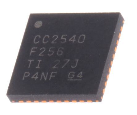
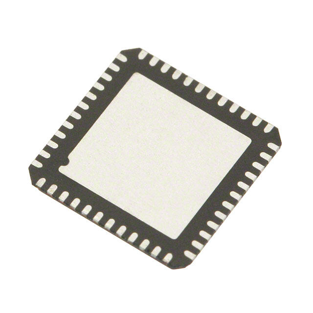
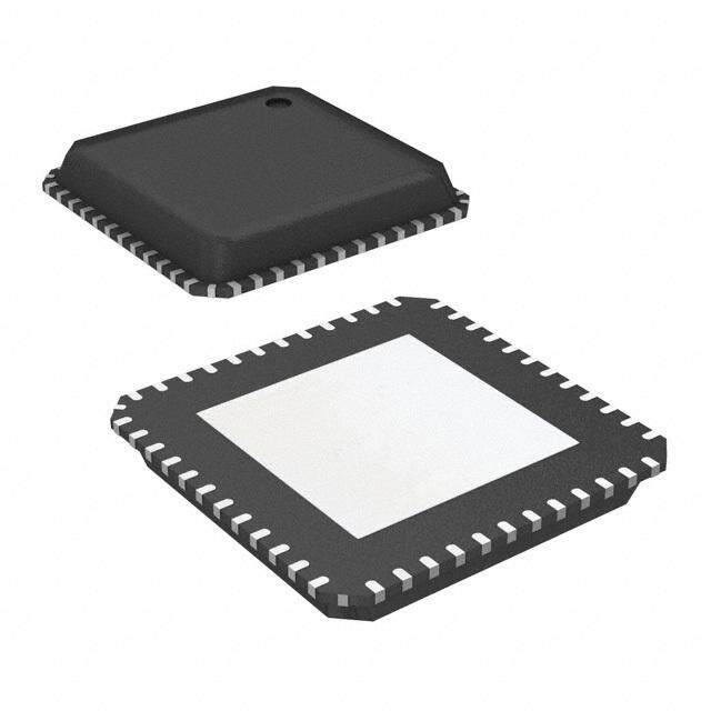
| 产品图片 |
|
| rohs | 符合RoHS无铅 / 符合限制有害物质指令(RoHS)规范要求 |
| 产品系列 | 射频微控制器 - MCU,Texas Instruments CC2540F256RHAT- |
| 数据手册 | 点击此处下载产品Datasheethttp://www.ti.com/lit/pdf/slyb174 |
| 产品型号 | CC2540F256RHAT |
| PCN封装 | |
| PCN设计/规格 | |
| 产品培训模块 | http://www.digikey.cn/PTM/IndividualPTM.page?site=cn&lang=zhs&ptm=25491 |
| 产品种类 | 射频微控制器 - MCU |
| 传输供电电流 | 31.6 mA |
| 其它名称 | 296-27922-6 |
| 制造商产品页 | http://www.ti.com/general/docs/suppproductinfo.tsp?distId=10&orderablePartNumber=CC2540F256RHAT |
| 功率-输出 | 8dBm |
| 包装 | Digi-Reel® |
| 可编程输入/输出端数量 | 21 |
| 商标 | Texas Instruments |
| 处理器系列 | CC2540 |
| 天线连接器 | PCB,表面贴装 |
| 存储容量 | 256kB 闪存,8kB RAM |
| 安装风格 | SMD/SMT |
| 定时器数量 | 3 Timer |
| 宽度 | 6 mm |
| 封装 | Reel |
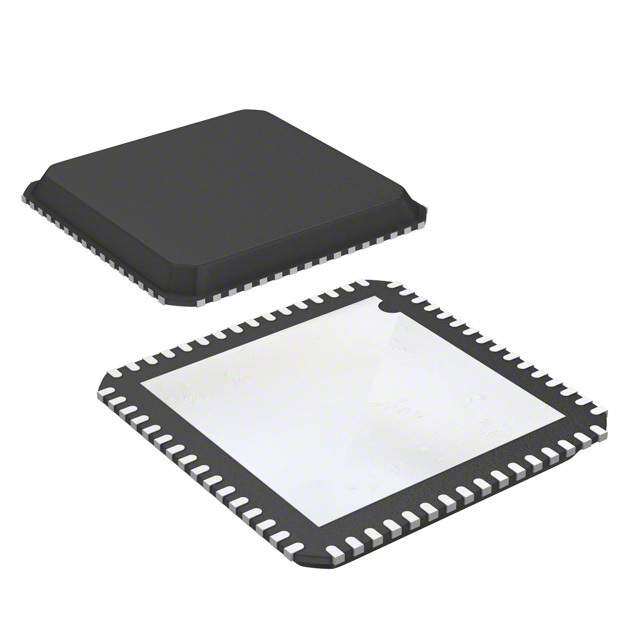
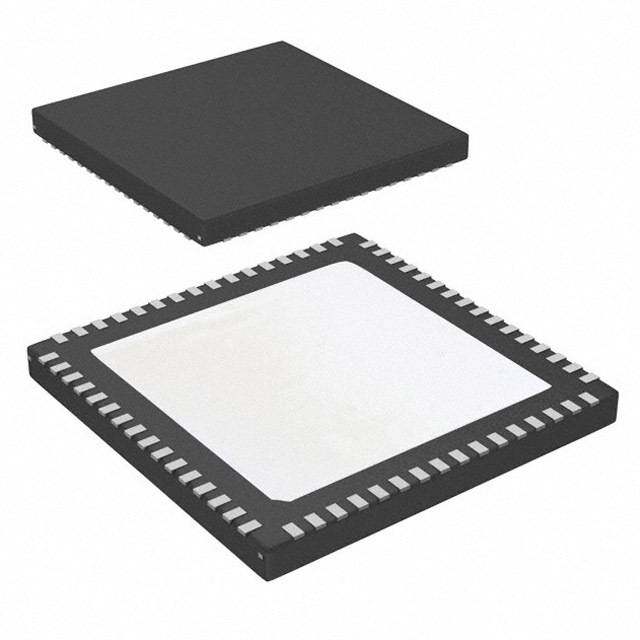
| 封装/外壳 | 40-VFQFN 裸露焊盘 |
| 封装/箱体 | VQFN-40 |
| 工作温度 | -40°C ~ 85°C |
| 工作温度范围 | - 40 C to + 85 C |
| 工作电源电压 | 2 V to 3.6 V |
| 工厂包装数量 | 250 |
| 应用 | 通用 |
| 接收供电电流 | 22.1 mA |
| 数据RAM大小 | 8 kB |
| 数据总线宽度 | 8 bit |
| 数据接口 | PCB,表面贴装 |
| 数据速率(最大值) | 1Mbps |
| 最大数据速率 | 1 Mbps |
| 标准包装 | 1 |
| 核心 | 8051 |
| 灵敏度 | -93dBm |
| 片上ADC | Yes |
| 电压-电源 | 2 V ~ 3.6 V |
| 电流-传输 | 31.6mA |
| 电流-接收 | 22.1mA |
| 程序存储器大小 | 256 kB |
| 类型 | Bluetooth |
| 系列 | CC2540 |
| 调制或协议 | 蓝牙 v4.0,低功耗 |
| 输入/输出端数量 | 21 I/O |
| 输出功率 | 8 dBm |
| 配用 | /product-detail/zh/CC2540DK-MINI/296-28079-ND/2503773/product-detail/zh/CC2540EMK/296-30819-ND/2696221/product-detail/zh/CC2540EMK-USB/296-30820-ND/2696222 |
| 长度 | 6 mm |
| 频率 | 2.4GHz |


- 商务部:美国ITC正式对集成电路等产品启动337调查
- 曝三星4nm工艺存在良率问题 高通将骁龙8 Gen1或转产台积电
- 太阳诱电将投资9.5亿元在常州建新厂生产MLCC 预计2023年完工
- 英特尔发布欧洲新工厂建设计划 深化IDM 2.0 战略
- 台积电先进制程称霸业界 有大客户加持明年业绩稳了
- 达到5530亿美元!SIA预计今年全球半导体销售额将创下新高
- 英特尔拟将自动驾驶子公司Mobileye上市 估值或超500亿美元
- 三星加码芯片和SET,合并消费电子和移动部门,撤换高东真等 CEO
- 三星电子宣布重大人事变动 还合并消费电子和移动部门
- 海关总署:前11个月进口集成电路产品价值2.52万亿元 增长14.8%


PDF Datasheet 数据手册内容提取
CC2540F128, CC2540F256 www.ti.com SWRS084F–OCTOBER2010–REVISEDJUNE2013 ® 2.4-GHz Bluetooth low energy System-on-Chip CheckforSamples:CC2540F128,CC2540F256 FEATURES A 1 • TrueSingle-ChipBLESolution:CC2540Can • TPS62730Compatible 23456 RunBothApplicationandBLEProtocolStack, LowPowerinActiveMode IncludesPeripheralstoInterfaceWithWide – RXDownto15.8mA(3VSupply) RangeofSensors,Etc. – TX(-6dBm):18.6mA(3VSupply) • 6-mm× 6-mmPackage A • RF • Microcontroller – Bluetoothlowenergytechnology – High-PerformanceandLow-Power8051 Compatible MicrocontrollerCore – ExcellentLinkBudget(upto97dB), – In-System-ProgrammableFlash,128KBor EnablingLong-RangeApplicationsWithout 256KB ExternalFrontEnd – 8-KBSRAM – AccurateDigitalReceivedSignal-Strength A Indicator(RSSI) • Peripherals – SuitableforSystemsTargetingCompliance – 12-BitADCwithEightChannelsand WithWorldwideRadioFrequency ConfigurableResolution Regulations:ETSIEN300328andEN300 – IntegratedHigh-PerformanceOp-Ampand 440Class2(Europe),FCCCFR47Part15 Ultralow-PowerComparator (US),andARIBSTD-T66(Japan) – General-PurposeTimers(One16-Bit,Two • Layout 8-Bit) – FewExternalComponents – 21General-PurposeI/OPins(19× 4mA,2× – ReferenceDesignProvided 20mA) – 6-mm ×6-mmQFN40Package – 32-kHzSleepTimerWithCapture • LowPower – TwoPowerfulUSARTsWithSupportfor – ActiveModeRXDownto19.6mA SeveralSerialProtocols – ActiveModeTX(–6dBm):24mA – Full-SpeedUSBInterface – PowerMode1(3-μsWake-Up):235 μA – IRGenerationCircuitry – PowerMode2(SleepTimerOn):0.9 μA – PowerfulFive-ChannelDMA – PowerMode3(ExternalInterrupts):0.4μA – AESSecurityCoprocessor – WideSupplyVoltageRange(2V–3.6V) – BatteryMonitorandTemperatureSensor – FullRAMandRegisterRetentioninAll – EachCC2540ContainsaUnique48-bit PowerModes IEEEAddress 1 Pleasebeawarethatanimportantnoticeconcerningavailability,standardwarranty,anduseincriticalapplicationsof TexasInstrumentssemiconductorproductsanddisclaimerstheretoappearsattheendofthisdatasheet. SmartRFisatrademarkofTexasInstruments. 2 BluetoothisaregisteredtrademarkofBluetoothSIG,Inc. 3 SupportedbyIAREmbeddedWorkbenchisatrademarkofIARSystemsAB. 4 ZigBeeisaregisteredtrademarkofZigBeeAlliance. 5 Allothertrademarksarethepropertyoftheirrespectiveowners. 6 PRODUCTIONDATAinformationiscurrentasofpublicationdate. Copyright©2010–2013,TexasInstrumentsIncorporated Products conform to specifications per the terms of the Texas Instruments standard warranty. Production processing does not necessarilyincludetestingofallparameters.
CC2540F128, CC2540F256 SWRS084F–OCTOBER2010–REVISEDJUNE2013 www.ti.com SOFTWARE FEATURES APPLICATIONS • Bluetoothv4.0CompliantProtocolStackfor • 2.4-GHzBluetoothlowenergySystems Single-ModeBLESolution • MobilePhoneAccessories – CompletePower-OptimizedStack, • SportsandLeisureEquipment IncludingControllerandHost • ConsumerElectronics – GAP –Central,Peripheral,Observer,or • HumanInterfaceDevices(Keyboard,Mouse, Broadcaster(IncludingCombination RemoteControl) Roles) • USBDongles – ATT/GATT –ClientandServer • HealthCareandMedical – SMP –AES-128Encryptionand Decryption CC2540 WITH TPS62730 – L2CAP • TPS62730isa2MHzStepDownConverter – SampleApplicationsandProfiles withBypassMode – GenericApplicationsforGAPCentral • ExtendsBatteryLifetimebyupto20% andPeripheralRoles • ReducedCurrentinTXandRX – Proximity,Accelerometer,SimpleKeys, • 30nABypassModeCurrenttoSupportLow andBatteryGATTServices PowerModes – MultipleConfigurationoptions • RFPerformanceUnchanged – Single-ChipConfiguration,Allowing • SmallPackageAllowsforSmallSolutionSize ApplicationtoRunonCC2540 • CC2540Controllable – NetworkProcessorInterfacefor ApplicationsRunningonanExternal Microcontroller – BTool– WindowsPCApplicationfor Evaluation,Development,andTest • DevelopmentTools – CC2540MiniDevelopmentKit – SmartRF™Software – SupportedbyIAREmbeddedWorkbench™ Softwarefor8051 DESCRIPTION The CC2540 is a cost-effective, low-power, true system-on-chip (SoC) for Bluetooth low energy applications. It enables robust BLE master or slave nodes to be built with very low total bill-of-material costs. The CC2540 combines an excellent RF transceiver with an industry-standard enhanced 8051 MCU, in-system programmable flash memory, 8-KB RAM, and many other powerful supporting features and peripherals. The CC2540 is suitable for systems where very low power consumption is required. Very low-power sleep modes are available. Short transitiontimesbetweenoperatingmodesfurtherenablelowpowerconsumption. The CC2540 comes in two different versions: CC2540F128/F256, with 128 and 256 KB of flash memory, respectively. Combined with the Bluetooth low energy protocol stack from Texas Instruments, the CC2540F128/F256 forms themarket’smostflexibleandcost-effectivesingle-modeBluetoothlowenergysolution. 2 SubmitDocumentationFeedback Copyright©2010–2013,TexasInstrumentsIncorporated ProductFolderLinks:CC2540F128 CC2540F256
CC2540F128, CC2540F256 www.ti.com SWRS084F–OCTOBER2010–REVISEDJUNE2013 WATCHDOG ON-CHIPVOLTAGE VDD (2 V–3.6 V) RESET_N RESET TIMER REGULATOR DCOUPL XOSC_Q2 32-MHz POWER-ON RESET XOSC_Q1 CRYSTALOSC CLOCK MUX BROWN OUT and s P2_4 32.768-kHz CALIBRATION Bu P2_3 CRYSTALOSC FR SLEEPTIMER S P2_2 DEBUG HIGH- 32-kHz P2_1 INTERFACE RSCP-EOESDC RC-OSC POWER MANAGEMENTCONTROLLER P2_0 PDATA P1_7 P1_6 8051 CPU XRAM P1_5 CORE IRAM MEMORY P1_4 ARBITRATOR FLASH FLASH SFR P1_3 P1_2 P1_1 DMA UNIFIED P1_0 IRQ CTRL FLASH CTRL P0_7 P0_6 ANALOG COMPARATOR P0_5 FIFOCTRL 1 KB SRAM P0_4 P0_3 OP-AMP biter P0_2 Ar P0_1 adio RADIO REGISTERS AES R P0_0 R ENCRYPTION LE DS AND OL ADC DECRYPTION Link Layer Engine R AUDIO/DC NT us O B C R O SF I/ H T DEMODULATOR N MODULATOR Y S USB_N USB USB_P USART0 USART1 RECEIVE UENCYESIZER TRANSMIT QH FRESYNT TIMER 1 (16-Bit) TIMER 2 (BLE LLTIMER) RF_P RF_N TIMER 3 (8-Bit) DIGITAL ANALOG TIMER 4 (8-Bit) MIXED B0301-05 Copyright©2010–2013,TexasInstrumentsIncorporated SubmitDocumentationFeedback 3 ProductFolderLinks:CC2540F128 CC2540F256
CC2540F128, CC2540F256 SWRS084F–OCTOBER2010–REVISEDJUNE2013 www.ti.com This integrated circuit can be damaged by ESD. Texas Instruments recommends that all integrated circuits be handled with appropriateprecautions.Failuretoobserveproperhandlingandinstallationprocedurescancausedamage. ESDdamagecanrangefromsubtleperformancedegradationtocompletedevicefailure.Precisionintegratedcircuitsmaybemore susceptibletodamagebecauseverysmallparametricchangescouldcausethedevicenottomeetitspublishedspecifications. ABSOLUTE MAXIMUM RATINGS(1) MIN MAX UNIT Supplyvoltage Allsupplypinsmusthavethesamevoltage –0.3 3.9 V –0.3 VDD+0.3, Voltageonanydigitalpin V ≤3.9 InputRFlevel 10 dBm Storagetemperaturerange –40 125 °C Allpads,accordingtohuman-bodymodel,JEDECSTD22,methodA114 2 kV ESD(2) Accordingtocharged-devicemodel,JEDECSTD22,methodC101 750 V (1) StressesbeyondthoselistedunderAbsoluteMaximumRatingsmaycausepermanentdamagetothedevice.Thesearestressratings only,andfunctionaloperationofthedeviceattheseoranyotherconditionsbeyondthoseindicatedunderRecommendedOperating Conditionsisnotimplied.Exposuretoabsolute-maximum-ratedconditionsforextendedperiodsmayaffectdevicereliability. (2) CAUTION:ESDsensitivedevice.Precautionsshouldbeusedwhenhandingthedeviceinordertopreventpermanentdamage. RECOMMENDED OPERATING CONDITIONS MIN MAX UNIT Operatingambienttemperaturerange,T –40 85 °C A Operatingsupplyvoltage 2 3.6 V ELECTRICAL CHARACTERISTICS MeasuredonTexasInstrumentsCC2540EMreferencedesignwithT =25°CandVDD=3V A PARAMETER TESTCONDITIONS MIN TYP MAX UNIT Powermode1.Digitalregulatoron;16-MHzRCOSCand32- MHzcrystaloscillatoroff;32.768-kHzXOSC,POR,BODand 235 sleeptimeractive;RAMandregisterretention Powermode2.Digitalregulatoroff;16-MHzRCOSCand32- µA MHzcrystaloscillatoroff;32.768-kHzXOSC,POR,andsleep 0.9 Icore Corecurrentconsumption timeractive;RAMandregisterretention Powermode3.Digitalregulatoroff;noclocks;PORactive; 0.4 RAMandregisterretention LowMCUactivity:32-MHzXOSCrunning.Noradioor 6.7 mA peripherals.Noflashaccess,noRAMaccess. Timer1.Timerrunning,32-MHzXOSCused 90 μA Timer2.Timerrunning,32-MHzXOSCused 90 μA Peripheralcurrentconsumption Timer3.Timerrunning,32-MHzXOSCused 60 μA I (AddstocorecurrentI foreach peri core peripheralunitactivated) Timer4.Timerrunning,32-MHzXOSCused 70 μA Sleeptimer,including32.753-kHzRCOSC 0.6 μA ADC,whenconverting 1.2 mA 4 SubmitDocumentationFeedback Copyright©2010–2013,TexasInstrumentsIncorporated ProductFolderLinks:CC2540F128 CC2540F256
CC2540F128, CC2540F256 www.ti.com SWRS084F–OCTOBER2010–REVISEDJUNE2013 GENERAL CHARACTERISTICS MeasuredonTexasInstrumentsCC2540EMreferencedesignwithT =25°CandVDD=3V A PARAMETER TESTCONDITIONS MIN TYP MAX UNIT WAKE-UPANDTIMING Digitalregulatoron,16-MHzRCOSCand32-MHzcrystal Powermode1→Active 4 μs oscillatoroff.Start-upof16-MHzRCOSC Digitalregulatoroff,16-MHzRCOSCand32-MHzcrystal Powermode2or3→Active 120 μs oscillatoroff.Start-upofregulatorand16-MHzRCOSC CrystalESR=16Ω.Initiallyrunningon16-MHzRCOSC, 410 μs Active→TXorRX with32-MHzXOSCOFF With32-MHzXOSCinitiallyon 160 μs RX/TXturnaround 150 μs RADIOPART RFfrequencyrange Programmablein2-MHzsteps 2402 2480 MHz Datarateandmodulationformat 1Mbps,GFSK,250kHzdeviation RF RECEIVE SECTION MeasuredonTexasInstrumentsCC2540EMreferencedesignwithT =25°C,VDD=3V,f =2440MHz A c 1Mbps,GFSK,250-kHzdeviation,Bluetoothlowenergymode,and0.1%BER(1) PARAMETER TESTCONDITIONS MIN TYP MAX UNIT Receiversensitivity(2) High-gainmode –93 dBm Receiversensitivity(2) Standardmode –87 dBm Saturation(3) 6 dBm Co-channelrejection(3) –5 dB Adjacent-channelrejection(3) ±1MHz –5 dB Alternate-channelrejection(3) ±2MHz 30 dB Blocking(3) –30 dBm Frequencyerrortolerance(4) Includingbothinitialtoleranceanddrift –250 250 kHz Symbolrateerrortolerance(5) –80 80 ppm Conductedmeasurementwitha50-Ωsingle-endedload. Spuriousemission.Onlylargestspurious ComplieswithEN300328,EN300440class2,FCCCFR47, –75 dBm emissionstatedwithineachband. Part15andARIBSTD-T-66 RXmode,standardmode,noperipheralsactive,lowMCU 19.6 activity,MCUat250kHz Currentconsumption mA RXmode,high-gainmode,noperipheralsactive,lowMCU 22.1 activity,MCUat250kHz (1) 0.1%BERmapsto30.8%PER (2) ThereceiversensitivitysettingisprogrammableusingaTIBLEstackvendor-specificAPIcommand.Thedefaultvalueisstandard mode. (3) Resultsbasedonstandardgainmode (4) DifferencebetweencenterfrequencyofthereceivedRFsignalandlocaloscillatorfrequency (5) Differencebetweenincomingsymbolrateandtheinternallygeneratedsymbolrate Copyright©2010–2013,TexasInstrumentsIncorporated SubmitDocumentationFeedback 5 ProductFolderLinks:CC2540F128 CC2540F256
CC2540F128, CC2540F256 SWRS084F–OCTOBER2010–REVISEDJUNE2013 www.ti.com RF TRANSMIT SECTION MeasuredonTexasInstrumentsCC2540EMreferencedesignwithT =25°C,VDD=3Vandf =2440MHz A c PARAMETER TESTCONDITIONS MIN TYP MAX UNIT Deliveredtoasingle-ended50-Ωloadthroughabalunusing 4 maximumrecommendedoutputpowersetting Outputpower dBm Deliveredtoasingle-ended50-Ωloadthroughabalunusingminimum –23 recommendedoutputpowersetting Programmableoutputpower Deliveredtoasingle-ended50Ωloadthroughabalun 27 dB range Conductedmeasurementwitha50-Ωsingle-endedload.Complies Spuriousemissions withEN300328,EN300440class2,FCCCFR47,Part15andARIB –41 dBm STD-T-66(1) TXmode,–23-dBmoutputpower,noperipheralsactive,lowMCU 21.1 activity,MCUat250kHz TXmode,–6-dBmoutputpower,noperipheralsactive,lowMCU 23.8 activity,MCUat250kHz Currentconsumption mA TXmode,0-dBmoutputpower,noperipheralsactive,lowMCU 27 activity,MCUat250kHz TXmode,4-dBmoutputpower,noperipheralsactive,lowMCU 31.6 activity,MCUat250kHz DifferentialimpedanceasseenfromtheRFport(RF_PandRF_N) Optimumloadimpedance 70+j30 Ω towardtheantenna (1) DesignswithantennaconnectorsthatrequireconductedETSIcomplianceat64MHzshouldinsertanLCresonatorinfrontofthe antennaconnector.Usea1.6-nHinductorinparallelwitha1.8-pFcapacitor.ConnectbothfromthesignaltracetoagoodRFground. CURRENT CONSUMPTION WITH TPS62730 MeasuredonTexasInstrumentsCC2540TPS62730EMreferencedesignwithT =25°C,VDD=3V,andf =2440MHZ. A c 1Mbps,GFSK,250kHzdeviation,Bluetooth™lowenergymode,1%BER(1) PARAMETER TESTCONDITIONS MIN TYP MAX UNIT RXmode,standardmode,noperipheralsactive,lowMCUactivity,MCUat1 15.8 MHZ RXmode,high-gainmode,noperipheralsactive,lowMCUactivity,MCUat1 17.8 MHZ TXmode,-23dBmoutputpower,noperipheralsactive,lowMCUactivity, 16.5 MCUat1MHZ CurrentConsumption mA TXmode,-6dBmoutputpower,noperipheralsactive,lowMCUactivity, 18.6 MCUat1MHZ TXmode,0dBmoutputpower,noperipheralsactive,lowMCUactivity, 21 MCUat1MHZ TXmode,4dBmoutputpower,noperipheralsactive,lowMCUactivity, 24.6 MCUat1MHZ (1) 0.1%BERmapsto30.8%PER 6 SubmitDocumentationFeedback Copyright©2010–2013,TexasInstrumentsIncorporated ProductFolderLinks:CC2540F128 CC2540F256
CC2540F128, CC2540F256 www.ti.com SWRS084F–OCTOBER2010–REVISEDJUNE2013 32-MHz CRYSTAL OSCILLATOR MeasuredonTexasInstrumentsCC2540EMreferencedesignwithT =25°CandVDD=3V A PARAMETER TESTCONDITIONS MIN TYP MAX UNIT Crystalfrequency 32 MHz Crystalfrequencyaccuracy requirement(1) –40 40 ppm ESR Equivalentseriesresistance 6 60 Ω C Crystalshuntcapacitance 1 7 pF 0 C Crystalloadcapacitance 10 16 pF L Start-uptime 0.25 ms Thecrystaloscillatormustbeinpowerdownfora guardtimebeforeitisusedagain.This Power-downguardtime requirementisvalidforallmodesofoperation.The 3 ms needforpower-downguardtimecanvarywith crystaltypeandload. (1) Includingagingandtemperaturedependency,asspecifiedby[1] 32.768-kHz CRYSTAL OSCILLATOR MeasuredonTexasInstrumentsCC2540EMreferencedesignwithT =25°CandVDD=3V A PARAMETER TESTCONDITIONS MIN TYP MAX UNIT Crystalfrequency 32.768 kHz Crystalfrequencyaccuracy requirement(1) –40 40 ppm ESR Equivalentseriesresistance 40 130 kΩ C Crystalshuntcapacitance 0.9 2 pF 0 C Crystalloadcapacitance 12 16 pF L Start-uptime 0.4 s (1) Includingagingandtemperaturedependency,asspecifiedby[1] 32-kHz RC OSCILLATOR MeasuredonTexasInstrumentsCC2540EMreferencedesignwithT =25°CandVDD=3V. ω PARAMETER TESTCONDITIONS MIN TYP MAX UNIT Calibratedfrequency(1) 32.753 kHz Frequencyaccuracyaftercalibration ±0.2% Temperaturecoefficient(2) 0.4 %/°C Supply-voltagecoefficient(3) 3 %/V Calibrationtime(4) 2 ms (1) Thecalibrated32-kHzRCoscillatorfrequencyisthe32-MHzXTALfrequencydividedby977. (2) Frequencydriftwhentemperaturechangesaftercalibration (3) Frequencydriftwhensupplyvoltagechangesaftercalibration (4) Whenthe32-kHzRCoscillatorisenabled,itiscalibratedwhenaswitchfromthe16-MHzRCoscillatortothe32-MHzcrystaloscillator isperformedwhileSLEEPCMD.OSC32K_CALDISissetto0. Copyright©2010–2013,TexasInstrumentsIncorporated SubmitDocumentationFeedback 7 ProductFolderLinks:CC2540F128 CC2540F256
CC2540F128, CC2540F256 SWRS084F–OCTOBER2010–REVISEDJUNE2013 www.ti.com 16-MHz RC OSCILLATOR MeasuredonTexasInstrumentsCC2540EMreferencedesignwithT =25°CandVDD=3V A PARAMETER TESTCONDITIONS MIN TYP MAX UNIT Frequency(1) 16 MHz Uncalibratedfrequencyaccuracy ±18% Calibratedfrequencyaccuracy ±0.6% Start-uptime 10 μs Initialcalibrationtime(2) 50 μs (1) Thecalibrated16-MHzRCoscillatorfrequencyisthe32-MHzXTALfrequencydividedby2. (2) Whenthe16-MHzRCoscillatorisenabled,itiscalibratedwhenaswitchfromthe16-MHzRCoscillatortothe32-MHzcrystaloscillator isperformedwhileSLEEPCMD.OSC_PDissetto0. RSSI CHARACTERISTICS MeasuredonTexasInstrumentsCC2540EMreferencedesignwithT =25°CandVDD=3V A PARAMETER TESTCONDITIONS MIN TYP MAX UNIT High-gainmode –99to–44 UsefulRSSIrange(1) dBm Standardmode –90to–35 AbsoluteuncalibratedRSSIaccuracy(1) High-gainmode ±4 dB Stepsize(LSBvalue) 1 dB (1) AssumingCC2540EMreferencedesign.OtherRFdesignsgiveanoffsetfromthereportedvalue. FREQUENCY SYNTHESIZER CHARACTERISTICS MeasuredonTexasInstrumentsCC2540EMreferencedesignwithT =25°C,VDD=3Vandf =2440MHz A c PARAMETER TESTCONDITIONS MIN TYP MAX UNIT At±1-MHzoffsetfromcarrier –109 Phasenoise,unmodulated At±3-MHzoffsetfromcarrier –112 dBc/Hz carrier At±5-MHzoffsetfromcarrier –119 ANALOG TEMPERATURE SENSOR MeasuredonTexasInstrumentsCC2540EMreferencedesignwithT =25°CandVDD=3V A PARAMETER TESTCONDITIONS MIN TYP MAX UNIT Output 1480 12-bit Temperaturecoefficient 4.5 /1°C Voltagecoefficient MeasuredusingintegratedADC,internalband-gapvoltage 1 /0.1V Initialaccuracywithoutcalibration reference,andmaximumresolution ±10 °C Accuracyusing1-pointcalibration ±5 °C Currentconsumptionwhenenabled 0.5 mA 8 SubmitDocumentationFeedback Copyright©2010–2013,TexasInstrumentsIncorporated ProductFolderLinks:CC2540F128 CC2540F256
CC2540F128, CC2540F256 www.ti.com SWRS084F–OCTOBER2010–REVISEDJUNE2013 OP-AMP CHARACTERISTICS T =25°C,VDD=3V,.AllmeasurementresultsareobtainedusingtheCC2540referencedesignspost-calibration. A PARAMETER TESTCONDITIONS MIN TYP MAX UNIT ChoppingConfiguration,RegisterAPCFG=0x07,OPAMPMC=0x03,OPAMPC=0x01 Outputmaximumvoltage VDD–0.1 V Outputminimumvoltage 0.1 V Open-loopgain 108 dB Gain-bandwidthproduct 2 MHz Slewrate 2.6 V/μs Inputmaximumvoltage VDD V Intputminimumvoltage 0 mV Inputoffsetvoltage 40 μV CMRR Common-moderejectionratio 90 dB Supplycurrent 0.4 mA f=0.01Hzto1Hz 1.1 Inputnoisevoltage nV/√(Hz) f=0.1Hzto10Hz 1.7 Non-ChoppingConfiguration,RegisterAPCFG=0x07,OPAMPMC=0x00,OPAMPC=0x01 Outputmaximumvoltage VDD–0.1 V Outputminimumvoltage 0.1 V Open-loopgain 108 dB Gain-bandwidthproduct 2 MHz Slewrate 2.6 V/μs Inputmaximumvoltage VDD V Intputminimumvoltage 0 mV Inputoffsetvoltage 3.2 mV CMRR Common-moderejectionratio 90 dB Supplycurrent 0.4 mA f=0.01Hzto1Hz 60 Inputnoisevoltage nV/√(Hz) f=0.1Hzto10Hz 65 COMPARATOR CHARACTERISTICS T =25°C,VDD=3V.AllmeasurementresultsareobtainedusingtheCC2540referencedesigns,post-calibration. A PARAMETER TESTCONDITIONS MIN TYP MAX UNIT Common-modemaximumvoltage VDD V Common-modeminimumvoltage –0.3 Inputoffsetvoltage 1 mV Offsetvstemperature 16 µV/°C Offsetvsoperatingvoltage 4 mV/V Supplycurrent 230 nA Hysteresis 0.15 mV Copyright©2010–2013,TexasInstrumentsIncorporated SubmitDocumentationFeedback 9 ProductFolderLinks:CC2540F128 CC2540F256
CC2540F128, CC2540F256 SWRS084F–OCTOBER2010–REVISEDJUNE2013 www.ti.com ADC CHARACTERISTICS T =25°CandVDD=3V A PARAMETER TESTCONDITIONS MIN TYP MAX UNIT Inputvoltage VDDisvoltageonAVDD5pin 0 VDD V Externalreferencevoltage VDDisvoltageonAVDD5pin 0 VDD V Externalreferencevoltagedifferential VDDisvoltageonAVDD5pin 0 VDD V Inputresistance,signal Simulatedusing4-MHzclockspeed 197 kΩ Full-scalesignal(1) Peak-to-peak,defines0dBFS 2.97 V Single-endedinput,7-bitsetting 5.7 Single-endedinput,9-bitsetting 7.5 Single-endedinput,10-bitsetting 9.3 Single-endedinput,12-bitsetting 10.3 Differentialinput,7-bitsetting 6.5 ENOB(1) Effectivenumberofbits bits Differentialinput,9-bitsetting 8.3 Differentialinput,10-bitsetting 10 Differentialinput,12-bitsetting 11.5 10-bitsetting,clockedbyRCOSC 9.7 12-bitsetting,clockedbyRCOSC 10.9 Usefulpowerbandwidth 7-bitsetting,bothsingleanddifferential 0–20 kHz Singleendedinput,12-bitsetting,–6 dBFS(1) –75.2 THD Totalharmonicdistortion dB Differentialinput,12-bitsetting,–6 dBFS(1) –86.6 Single-endedinput,12-bitsetting(1) 70.2 Differentialinput,12-bitsetting(1) 79.3 Signaltononharmonicratio SdBinFgSle(-1e)ndedinput,12-bitsetting,–6 78.8 dB Differentialinput,12-bitsetting,–6 dBFS(1) 88.9 Differentialinput,12-bitsetting,1-kHz CMRR Common-moderejectionratio >84 dB sine(0dBFS),limitedbyADCresolution Singleendedinput,12-bitsetting,1-kHz Crosstalk >84 dB sine(0dBFS),limitedbyADCresolution Offset Midscale –3 mV Gainerror 0.68% 12-bitsetting,mean(1) 0.05 DNL Differentialnonlinearity LSB 12-bitsetting,maximum(1) 0.9 12-bitsetting,mean(1) 4.6 12-bitsetting,maximum(1) 13.3 INL Integralnonlinearity LSB 12-bitsetting,mean,clockedbyRCOSC 10 12-bitsetting,max,clockedbyRCOSC 29 Singleendedinput,7-bitsetting(1) 35.4 Singleendedinput,9-bitsetting(1) 46.8 Singleendedinput,10-bitsetting(1) 57.5 SINAD Singleendedinput,12-bitsetting(1) 66.6 Signal-to-noise-and-distortion dB (–THD+N) Differentialinput,7-bitsetting(1) 40.7 Differentialinput,9-bitsetting(1) 51.6 Differentialinput,10-bitsetting(1) 61.8 Differentialinput,12-bitsetting(1) 70.8 (1) Measuredwith300-Hzsine-waveinputandVDDasreference. 10 SubmitDocumentationFeedback Copyright©2010–2013,TexasInstrumentsIncorporated ProductFolderLinks:CC2540F128 CC2540F256
CC2540F128, CC2540F256 www.ti.com SWRS084F–OCTOBER2010–REVISEDJUNE2013 ADC CHARACTERISTICS (continued) T =25°CandVDD=3V A PARAMETER TESTCONDITIONS MIN TYP MAX UNIT 7-bitsetting 20 9-bitsetting 36 Conversiontime μs 10-bitsetting 68 12-bitsetting 132 Powerconsumption 1.2 mA InternalreferenceVDDcoefficient 4 mV/V Internalreferencetemperaturecoefficient 0.4 mV/10°C Internalreferencevoltage 1.24 V CONTROL INPUT AC CHARACTERISTICS T =–40°Cto85°C,VDD=2Vto3.6V. A PARAMETER TESTCONDITIONS MIN TYP MAX UNIT Theundividedsystemclockis32MHzwhencrystaloscillatorisused. Systemclock,f SYSCLK Theundividedsystemclockis16MHzwhencalibrated16-MHzRC 16 32 MHz t =1/f SYSCLK SYSCLK oscillatorisused. Seeitem1,Figure1.Thisistheshortestpulsethatisrecognizedas acompleteresetpinrequest.Notethatshorterpulsesmaybe RESET_Nlowduration 1 µs recognizedbutdonotleadtocompleteresetofallmoduleswithinthe chip. Seeitem2,Figure1.Thisistheshortestpulsethatisrecognizedas Interruptpulseduration 20 ns aninterruptrequest. RESET_N 1 2 Px.n T0299-01 Figure1. ControlInputACCharacteristics Copyright©2010–2013,TexasInstrumentsIncorporated SubmitDocumentationFeedback 11 ProductFolderLinks:CC2540F128 CC2540F256
CC2540F128, CC2540F256 SWRS084F–OCTOBER2010–REVISEDJUNE2013 www.ti.com SPI AC CHARACTERISTICS T =–40°Cto85°C,VDD=2Vto3.6V A PARAMETER TESTCONDITIONS MIN TYP MAX UNIT Master,RXandTX 250 t SCKperiod ns 1 Slave,RXandTX 250 SCKdutycycle Master 50% Master 63 t SSNlowtoSCK ns 2 Slave 63 Master 63 t SCKtoSSNhigh ns 3 Slave 63 t MOSIearlyout Master,load=10pF 7 ns 4 t MOSIlateout Master,load=10pF 10 ns 5 t MISOsetup Master 90 ns 6 t MISOhold Master 10 ns 7 SCKdutycycle Slave 50% ns t MOSIsetup Slave 35 ns 10 t MOSIhold Slave 10 ns 11 t MISOlateout Slave,load=10pF 95 ns 9 Master,TXonly 8 Master,RXandTX 4 Operatingfrequency MHz Slave,RXonly 8 Slave,RXandTX 4 SCK t t 2 3 SSN t t 4 5 MOSI D0 X D1 t t 6 7 MISO X D0 X T0478-01 Figure2. SPIMasterACCharacteristics 12 SubmitDocumentationFeedback Copyright©2010–2013,TexasInstrumentsIncorporated ProductFolderLinks:CC2540F128 CC2540F256
CC2540F128, CC2540F256 www.ti.com SWRS084F–OCTOBER2010–REVISEDJUNE2013 SCK t t 2 3 SSN t t 8 9 MISO D0 X D1 t t 10 11 MOSI X D0 X T0479-01 Figure3. SPISlaveACCharacteristics Copyright©2010–2013,TexasInstrumentsIncorporated SubmitDocumentationFeedback 13 ProductFolderLinks:CC2540F128 CC2540F256
CC2540F128, CC2540F256 SWRS084F–OCTOBER2010–REVISEDJUNE2013 www.ti.com DEBUG INTERFACE AC CHARACTERISTICS T =–40°Cto85°C,VDD=2Vto3.6V A PARAMETER TESTCONDITIONS MIN TYP MAX UNIT f Debugclockfrequency(seeFigure4) 12 MHz clk_dbg t Allowedhighpulseonclock(seeFigure4) 35 ns 1 t Allowedlowpulseonclock(seeFigure4) 35 ns 2 EXT_RESET_Nlowtofirstfallingedgeondebug t 167 ns 3 clock(seeFigure6) FallingedgeonclocktoEXT_RESET_Nhigh(see t 83 ns 4 Figure6) EXT_RESET_Nhightofirstdebugcommand(see t 83 ns 5 Figure6) t Debugdatasetup(seeFigure5) 2 ns 6 t Debugdatahold(seeFigure5) 4 ns 7 t Clock-to-datadelay(seeFigure5) Load=10pF 30 ns 8 Time DEBUG_CLK P2_2 t t 1 2 1/f clk_dbg T0436-01 Figure4. DebugClock– BasicTiming Time DEBUG_CLK P2_2 RESET_N t t t 3 4 5 T0437-01 Figure5. DebugEnableTiming 14 SubmitDocumentationFeedback Copyright©2010–2013,TexasInstrumentsIncorporated ProductFolderLinks:CC2540F128 CC2540F256
CC2540F128, CC2540F256 www.ti.com SWRS084F–OCTOBER2010–REVISEDJUNE2013 Time DEBUG_CLK P2_2 DEBUG_DATA (to CC2540) P2_1 DEBUG_DATA (from CC2540) P2_1 t t t 6 7 8 T0438-02 Figure6. DataSetupandHoldTiming TIMER INPUTS AC CHARACTERISTICS T =–40°Cto85°C,VDD=2Vto3.6V A PARAMETER TESTCONDITIONS MIN TYP MAX UNIT Synchronizersdeterminetheshortestinputpulsethatcanbe Inputcapturepulseduration recognized.Thesynchronizersoperateatthecurrentsystemclockrate 1.5 t SYSCLK (16MHzor32MHz). DC CHARACTERISTICS T =25°C,VDD=3V A PARAMETER TESTCONDITIONS MIN TYP MAX UNIT Logic-0inputvoltage 0.5 V Logic-1inputvoltage 2.5 V Logic-0inputcurrent Inputequals0V –50 50 nA Logic-1inputcurrent InputequalsVDD –50 50 nA I/O-pinpullupandpulldownresistors 20 kΩ Logic-0outputvoltage,4-mApins Outputload4mA 0.5 V Logic-1outputvoltage,4-mApins Outputload4mA 2.4 V Copyright©2010–2013,TexasInstrumentsIncorporated SubmitDocumentationFeedback 15 ProductFolderLinks:CC2540F128 CC2540F256
CC2540F128, CC2540F256 SWRS084F–OCTOBER2010–REVISEDJUNE2013 www.ti.com DEVICE INFORMATION PIN DESCRIPTIONS TheCC2540pinoutisshowninFigure7andashortdescriptionofthepinsfollows. CC2540 RHAPackage (Top View) 2 1 Q Q _ _ K K 2 2 3 3 C C S S O O COUPL VDD1 1_6 1_7 2_0 2_1 2_2 2_3 / X 2_4 / X VDD6 D D P P P P P P P A 40 39 38 37 36 35 34 33 32 31 DGND_USB 1 30 R_BIAS USB_P 2 29 AVDD4 USB_N 3 28 AVDD1 DVDD_USB 4 27 AVDD2 P1_5 5 GND 26 RF_N P1_4 6 Ground Pad 25 RF_P P1_3 7 24 AVDD3 P1_2 8 23 XOSC_Q2 P1_1 9 22 XOSC_Q1 DVDD2 10 21 AVDD5 11 12 13 14 15 16 17 18 19 20 0 7 6 5 4 3 2 1 0 N P1_ P0_ P0_ P0_ P0_ P0_ P0_ P0_ P0_ ET_ S E R P0076-05 NOTE: Theexposedgroundpadmustbeconnectedtoasolidgroundplane,asthisisthegroundconnectionforthechip. Figure7. PinoutTopView 16 SubmitDocumentationFeedback Copyright©2010–2013,TexasInstrumentsIncorporated ProductFolderLinks:CC2540F128 CC2540F256
CC2540F128, CC2540F256 www.ti.com SWRS084F–OCTOBER2010–REVISEDJUNE2013 PINDESCRIPTIONS PINNAME PIN PINTYPE DESCRIPTION AVDD1 28 Power(analog) 2-V–3.6-Vanalogpower-supplyconnection AVDD2 27 Power(analog) 2-V–3.6-Vanalogpower-supplyconnection AVDD3 24 Power(analog) 2-V–3.6-Vanalogpower-supplyconnection AVDD4 29 Power(analog) 2-V–3.6-Vanalogpower-supplyconnection AVDD5 21 Power(analog) 2-V–3.6-Vanalogpower-supplyconnection AVDD6 31 Power(analog) 2-V–3.6-Vanalogpower-supplyconnection DCOUPL 40 Power(digital) 1.8-Vdigitalpower-supplydecoupling.Donotuseforsupplyingexternalcircuits. DGND_USB 1 Groundpin ConnecttoGND DVDD_USB 4 Power(digital) 2-V–3.6-Vdigitalpower-supplyconnection DVDD1 39 Power(digital) 2-V–3.6-Vdigitalpower-supplyconnection DVDD2 10 Power(digital) 2-V–3.6-Vdigitalpower-supplyconnection GND — Ground Thegroundpadmustbeconnectedtoasolidgroundplane. P0_0 19 DigitalI/O Port0.0 P0_1 18 DigitalI/O Port0.1 P0_2 17 DigitalI/O Port0.2 P0_3 16 DigitalI/O Port0.3 P0_4 15 DigitalI/O Port0.4 P0_5 14 DigitalI/O Port0.5 P0_6 13 DigitalI/O Port0.6 P0_7 12 DigitalI/O Port0.7 P1_0 11 DigitalI/O Port1.0–20-mAdrivecapability P1_1 9 DigitalI/O Port1.1–20-mAdrivecapability P1_2 8 DigitalI/O Port1.2 P1_3 7 DigitalI/O Port1.3 P1_4 6 DigitalI/O Port1.4 P1_5 5 DigitalI/O Port1.5 P1_6 38 DigitalI/O Port1.6 P1_7 37 DigitalI/O Port1.7 P2_0 36 DigitalI/O Port2.0 P2_1 35 DigitalI/O Port2.1 P2_2 34 DigitalI/O Port2.2 P2_3/ 33 DigitalI/O, Port2.3/32.768kHzXOSC XOSC32K_Q2 AnalogI/O P2_4/ 32 DigitalI/O, Port2.4/32.768kHzXOSC XOSC32K_Q1 AnalogI/O RBIAS 30 AnalogI/O Externalprecisionbiasresistorforreferencecurrent RESET_N 20 Digitalinput Reset,active-low RF_N 26 RFI/O NegativeRFinputsignaltoLNAduringRX NegativeRFoutputsignalfromPAduringTX RF_P 25 RFI/O PositiveRFinputsignaltoLNAduringRX PositiveRFoutputsignalfromPAduringTX USB_N 3 DigitalI/O USBN USB_P 2 DigitalI/O USBP XOSC_Q1 22 AnalogI/O 32-MHzcrystaloscillatorpin1orexternal-clockinput XOSC_Q2 23 AnalogI/O 32-MHzcrystaloscillatorpin2 Copyright©2010–2013,TexasInstrumentsIncorporated SubmitDocumentationFeedback 17 ProductFolderLinks:CC2540F128 CC2540F256
CC2540F128, CC2540F256 SWRS084F–OCTOBER2010–REVISEDJUNE2013 www.ti.com BLOCK DIAGRAM A block diagram of the CC2540 is shown in Figure 8. The modules can be roughly divided into one of three categories: CPU-related modules; modules related to power, test, and clock distribution; and radio-related modules.Inthefollowingsubsections,ashortdescriptionofeachmoduleisgiven. RESET_N RESET WATTICMHEDROG ONR-CEHGIPULVAOTLOTRAGE VDDCDO U(2P VL–3.6 V) XOSC_Q2 32-MHz POWER-ON RESET XOSC_Q1 CRYSTALOSC CLOCK MUX BROWN OUT and P2_4 32.768-kHz CALIBRATION Bus P2_3 CRYSTALOSC FR SLEEPTIMER S P2_2 DEBUG HIGH- 32-kHz P2_1 INTERFACE RSCP-EOESDC RC-OSC POWER MANAGEMENTCONTROLLER P2_0 PDATA P1_7 P1_6 8051 CPU XRAM P1_5 CORE IRAM MEMORY P1_4 ARBITRATOR FLASH FLASH SFR P1_3 P1_2 P1_1 DMA UNIFIED P1_0 IRQ CTRL FLASH CTRL P0_7 P0_6 ANALOG COMPARATOR P0_5 FIFOCTRL 1 KB SRAM P0_4 P0_3 OP-AMP biter P0_2 Ar P0_1 adio RADIO REGISTERS AES R P0_0 R ENCRYPTION LE DS AND OL ADC DECRYPTION Link Layer Engine R AUDIO/DC NT us CO R B O SF I/ H T DEMODULATOR N MODULATOR Y S USB_N USB USB_P USART0 USART1 RECEIVE FREQUENCYSYNTHESIZER TRANSMIT TIMER 1 (16-Bit) TIMER 2 (BLE LLTIMER) RF_P RF_N TIMER 3 (8-Bit) DIGITAL ANALOG TIMER 4 (8-Bit) MIXED B0301-05 Figure8. CC2540BlockDiagram 18 SubmitDocumentationFeedback Copyright©2010–2013,TexasInstrumentsIncorporated ProductFolderLinks:CC2540F128 CC2540F256
CC2540F128, CC2540F256 www.ti.com SWRS084F–OCTOBER2010–REVISEDJUNE2013 BLOCK DESCRIPTIONS CPUandMemory The 8051 CPU core is a single-cycle 8051-compatible core. It has three different memory access busses (SFR, DATA,andCODE/XDATA),adebuginterface,andan18-inputextendedinterruptunit. The memory arbiter is at the heart of the system, as it connects the CPU and DMA controller with the physical memories and all peripherals through the SFR bus. The memory arbiter has four memory-access points, access of which can map to one of three physical memories: an SRAM, flash memory, and XREG/SFR registers. It is responsible for performing arbitration and sequencing between simultaneous memory accesses to the same physicalmemory. The SFR bus is drawn conceptually in Figure 8 as a common bus that connects all hardware peripherals to the memory arbiter. The SFR bus in the block diagram also provides access to the radio registers in the radio registerbank,eventhoughtheseareindeedmappedintoXDATAmemoryspace. The 8-KB SRAM maps to the DATA memory space and to parts of the XDATA memory spaces. The SRAM is an ultralow-power SRAM that retains its contents even when the digital part is powered off (power modes 2 and 3). The 128/256 KB flash block provides in-circuit programmable non-volatile program memory for the device, and mapsintotheCODEandXDATAmemoryspaces. Peripherals Writing to the flash block is performed through a flash controller that allows page-wise erasure and 4-bytewise programming.SeeUserGuidefordetailsontheflashcontroller. A versatile five-channel DMA controller is available in the system, accesses memory using the XDATA memory space, and thus has access to all physical memories. Each channel (trigger, priority, transfer mode, addressing mode, source and destination pointers, and transfer count) is configured with DMA descriptors that can be located anywhere in memory. Many of the hardware peripherals (AES core, flash controller, USARTs, timers, ADC interface, etc.) can be used with the DMA controller for efficient operation by performing data transfers betweenasingleSFRorXREGaddressandflash/SRAM. Each CC2540 contains a unique 48-bit IEEE address that can be used as the public device address for a Bluetooth device. Designers are free to use this address, or provide their own, as described in the Bluetooth specfication. The interrupt controller services a total of 18 interrupt sources, divided into six interrupt groups, each of which is associated with one of four interrupt priorities. I/O and sleep timer interrupt requests are serviced even if the deviceisinasleepmode(powermodes1and2)bybringingtheCC2540backtotheactivemode. The debug interface implements a proprietary two-wire serial interface that is used for in-circuit debugging. Through this debug interface, it is possible to erase or program the entire flash memory, control which oscillators are enabled, stop and start execution of the user program, execute instructions on the 8051 core, set code breakpoints, and single-step through instructions in the code. Using these techniques, it is possible to perform in- circuitdebuggingandexternalflashprogrammingelegantly. The I/O controller is responsible for all general-purpose I/O pins. The CPU can configure whether peripheral modulescontrolcertainpinsorwhethertheyareundersoftwarecontrol,andifso,whethereachpinisconfigured as an input or output and if a pullup or pulldown resistor in the pad is connected. Each peripheral that connects totheI/OpinscanchoosebetweentwodifferentI/Opinlocationstoensureflexibilityinvariousapplications. The sleep timer is an ultralow-power timer that can either use an external 32.768-kHz crystal oscillator or an internal 32.753-kHz RC oscillator. The sleep timer runs continuously in all operating modes except power mode 3. Typical applications of this timer are as a real-time counter or as a wake-up timer to get out of power modes 1 or2. A built-in watchdog timer allows the CC2540 to reset itself if the firmware hangs. When enabled by software, thewatchdogtimermustbeclearedperiodically;otherwise,itresetsthedevicewhenittimesout. Copyright©2010–2013,TexasInstrumentsIncorporated SubmitDocumentationFeedback 19 ProductFolderLinks:CC2540F128 CC2540F256
CC2540F128, CC2540F256 SWRS084F–OCTOBER2010–REVISEDJUNE2013 www.ti.com Timer 1 is a 16-bit timer with timer/counter/PWM functionality. It has a programmable prescaler, a 16-bit period value, and five individually programmable counter/capture channels, each with a 16-bit compare value. Each of the counter/capture channels can be used as a PWM output or to capture the timing of edges on input signals. It can also be configured in IR generation mode, where it counts timer 3 periods and the output is ANDed with the outputoftimer3togeneratemodulatedconsumerIRsignalswithminimalCPUinteraction. Timer 2 is a 40-bit timer used by theBluetooth low energy stack. It has a 16-bit counter with a configurable timer period and a 24-bit overflow counter that can be used to keep track of the number of periods that have transpired. A 40-bit capture register is also used to record the exact time at which a start-of-frame delimiter is received/transmitted or the exact time at which transmission ends. There are two 16-bit timer-compare registers and two 24-bit overflow-compare registers that can be used to give exact timing for start of RX or TX to the radio orgeneralinterrupts. Timer3andtimer4are8-bittimerswithtimer/counter/PWMfunctionality.Theyhaveaprogrammableprescaler, an 8-bit period value, and one programmable counter channel with an 8-bit compare value. Each of the counter channelscanbeusedasPWMoutput. USART 0 and USART 1 are each configurable as either an SPI master/slave or a UART. They provide double buffering on both RX and TX and hardware flow control and are thus well suited to high-throughput full-duplex applications. Each USART has its own high-precision baud-rate generator, thus leaving the ordinary timers free for other uses. When configured as SPI slaves, the USARTs sample the input signal using SCK directly instead ofusingsomeoversamplingscheme,andarethuswell-suitedforhighdatarates. The AES encryption/decryption core allows the user to encrypt and decrypt data using the AES algorithm with 128-bit keys. The AES core also supports ECB, CBC, CFB, OFB, CTR, and CBC-MAC, as well as hardware supportforCCM. The ADC supports 7 to 12 bits of resolution with a corresponding range of bandwidths from 30-kHz to 4-kHz, respectively. DC and audio conversions with up to eight input channels (I/O controller pins) are possible. The inputs can be selected as single-ended or differential. The reference voltage can be internal, AVDD, or a single- ended or differential external signal. The ADC also has a temperature-sensor input channel. The ADC can automatetheprocessofperiodicsamplingorconversionoverasequenceofchannels. Theoperationalamplifierisintendedtoprovidefront-endbufferingandgainfortheADC.Bothinputsaswellas the output are available on pins, so the feedback network is fully customizable. A chopper-stabilized mode is availableforapplicationsthatneedgoodaccuracywithhighgain. The ultralow-power analog comparator enables applications to wake up from PM2 or PM3 based on an analog signal. Both inputs are brought out to pins; the reference voltage must be provided externally. The comparator output is connected to the I/O controller interrupt detector and can be treated by the MCU as a regular I/O pin interrupt. 20 SubmitDocumentationFeedback Copyright©2010–2013,TexasInstrumentsIncorporated ProductFolderLinks:CC2540F128 CC2540F256
CC2540F128, CC2540F256 www.ti.com SWRS084F–OCTOBER2010–REVISEDJUNE2013 TYPICAL CHARACTERISTICS RXCURRENTINWAITFORSYNC TXCURRENT vs vs TEMPERATURE TEMPERATURE 20.5 32.5 Gain = Standard Setting TX Power Setting = 4 dBm Input = -70 dBm VCC = 3 V VCC = 3 V 20 32 A) A) m m nt ( 19.5 nt ( 31.5 e e urr urr C C 19 31 18.5 30.5 -40 -20 0 20 40 60 80 -40 -20 0 20 40 60 80 Temperature (°C) Temperature (°C) G001 G002 Figure9. Figure10. RXSENSITIVITY TXPOWER vs vs TEMPERATURE TEMPERATURE -83 7 Gain = Standard Setting TX Power Setting = 4 dBm -84 VCC = 3 V 6 VCC = 3 V -85 5 -86 m) m) B -87 B 4 d d vel ( -88 vel ( 3 e e L L -89 2 -90 1 -91 -92 0 -40 -20 0 20 40 60 80 -40 -20 0 20 40 60 80 Temperature (°C) Temperature (°C) G003 G004 Figure11. Figure12. RXCURRENTINWAITFORSYNC TXCURRENT vs vs SUPPLYVOLTAGE SUPPLYVOLTAGE 19.7 32 19.68 Gain = Standard Setting 31.9 TA = 25°C Input = -70 dBm TX Power Setting = 4 dBm 19.66 TA = 25°C 31.8 19.64 31.7 A) 19.62 A) 31.6 m m nt ( 19.6 nt ( 31.5 e e urr 19.58 urr 31.4 C C 19.56 31.3 19.54 31.2 19.52 31.1 19.5 31 2 2.2 2.4 2.6 2.8 3 3.2 3.4 3.6 2 2.2 2.4 2.6 2.8 3 3.2 3.4 3.6 Supply Voltage (V) Supply Voltage (V) G005 G006 Figure13. Figure14. Copyright©2010–2013,TexasInstrumentsIncorporated SubmitDocumentationFeedback 21 ProductFolderLinks:CC2540F128 CC2540F256
CC2540F128, CC2540F256 SWRS084F–OCTOBER2010–REVISEDJUNE2013 www.ti.com TYPICAL CHARACTERISTICS (continued) RXSENSITIVITY TXPOWER vs vs SUPPLYVOLTAGE SUPPLYVOLTAGE -87 5 -87.2 Gain = Standard Setting 4.8 TA = 25°C TA = 25°C TX Power Setting = 4 dBm -87.4 4.6 -87.6 4.4 m) -87.8 m) 4.2 B B el (d -88 el (d 4 ev -88.2 ev 3.8 L L -88.4 3.6 -88.6 3.4 -88.8 3.2 -89 3 2 2.2 2.4 2.6 2.8 3 3.2 3.4 3.6 2 2.2 2.4 2.6 2.8 3 3.2 3.4 3.6 Supply Voltage (V) Supply Voltage (V) G007 G008 Figure15. Figure16. RXSENSITIVITY RXINTERFERERREJECTION(SELECTIVITY) vs vs FREQUENCY INTERFERERFREQUENCY -87 60 -87.2 Gain = Standard Setting TA = 25°C 50 -87.4 VCC = 3 V -87.6 40 Level (dBm) --88-878..828 Rejection (dB) 2300 -88.4 10 GTAa i=n 2=5 S°Ctandard Setting -88.6 VCC = 3 V 0 Wanted Signal at 2426 MHz -88.8 with -67 dBm Level -89 -10 2400 2410 2420 2430 2440 2450 2460 2470 2480 2400 2410 2420 2430 2440 2450 2460 2470 2480 Frequency (MHz) Frequency (MHz) G009 G010 Figure17. Figure18. TXPOWER vs FREQUENCY 5 4.8 TA = 25°C TX Power Setting = 4 dBm 4.6 VCC = 3 V 4.4 m) 4.2 B el (d 4 ev 3.8 L 3.6 3.4 3.2 3 2400 2410 2420 2430 2440 2450 2460 2470 2480 Frequency (MHz) G011 Figure19. 22 SubmitDocumentationFeedback Copyright©2010–2013,TexasInstrumentsIncorporated ProductFolderLinks:CC2540F128 CC2540F256
CC2540F128, CC2540F256 www.ti.com SWRS084F–OCTOBER2010–REVISEDJUNE2013 TYPICAL CHARACTERISTICS (continued) Table1.OutputPowerandCurrentConsumption(1)(2) TypicalCurrentConsumptionWith TypicalOutputPower(dBm) TypicalCurrentConsumption(mA) TPS62730(mA) 4 32 24.6 0 27 21 –6 24 18.5 –23 21 16.5 (1) MeasuredonTexasInstrumentsCC2540EMreferencedesignwithT =25°C,VDD=3Vandf =2440MHz.SeeSWRU191for A c recommendedregistersettings (2) MeasuredonTexasInstrumentsCC2540TPS62730EMreferencedesignwithT =25°C,VDD=3Vandf =2440MHz.See A c SWRU191forrecommendedregistersettings TYPICAL CURRENT SAVINGS CC2540 Current Consumption CC2540 Current Consumption TX 4dBm RX SG CLKCONMOD0x80 35 40 25 40 30 35 35 Current(mA) 11220505 1122305050 CurrentSavings(%) DD%CCC//DDuCCrrOOenNFtFSavings Current(mA) 112050 12235050 CurrentSavings(%) DDCCCur//DDreCCntOOSNFaFvings 10 5 5 5 5 0 0 2.1 2.4 2.7 3 3.3 3.6 0 0 2.1 2.4 2.7 3 3.3 3.6 Supply(V) Supply(V) Figure20.CurrentSavingsinTXatRoomTemperature Figure21.CurrentSavingsinRXatRoomTemperature The application note (SWRA365) has information regarding the CC2540 and TPS62730 como board and the currentsavingsthatcanbeachievedusingthecomoboard. Copyright©2010–2013,TexasInstrumentsIncorporated SubmitDocumentationFeedback 23 ProductFolderLinks:CC2540F128 CC2540F256
CC2540F128, CC2540F256 SWRS084F–OCTOBER2010–REVISEDJUNE2013 www.ti.com APPLICATION INFORMATION Few external components are required for the operation of the CC2540. A typical application circuit is shown in Figure22. 32-kHzCrystal(1) C331 2-V to 3.6-V Power Supply C401 2 L A T X C321 40 39 38 37 36 35 34 33 32 31 1 DGND_UDCOUPLSB DVDD1 P1_6 P1_7 P2_0 P2_1 P2_2 OSC32K_Q2 OSC32K_Q1 AVDD6 RBIAS 30 R301 L251 2 USB_P P2_3/X P2_4/X AAVVDDDD41 2289 C251 C252 A(n5t0enWn)a 3 USB_N AVDD2 27 4 DVDD_USB L252 L253 RF_N 26 5 P1_5 CC2540 6 P1_4 RF_P 25 C261 L261 DIEATTACHPAD AVDD3 24 7 P1_3 XOSC_Q2 23 C262 C253 8 P1_2 XOSC_Q1 22 9 P1_1 N AVDD5 21 10 DVDD2 _ T 1_0 0_7 0_6 0_5 0_4 0_3 0_2 0_1 0_0 ESE P P P P P P P P P R 11 12 13 14 15 16 17 18 19 20 XTAL1 Power Supply Decoupling Capacitors are Not Shown C221 C231 Digital I/O Not Connected S0383-03 (1)32-kHzcrystalismandatorywhenrunningthechipinlow-powermodes,exceptifthelinklayerisinthestandby state(Vol.6PartBSection1.1in[1]). NOTE:Differentantennaalternativeswillbeprovidedasreferencedesigns. Figure22. CC2540ApplicationCircuit Table2.OverviewofExternalComponents(ExcludingSupplyDecouplingCapacitors) Component Description Value C221 32-MHzxtalloadingcapacitor 12pF C231 32-MHzxtalloadingcapacitor 12pF C251 PartoftheRFmatchingnetwork 18pF C252 PartoftheRFmatchingnetwork 1pF C253 PartoftheRFmatchingnetwork 1pF C261 PartoftheRFmatchingnetwork 18pF C262 PartoftheRFmatchingnetwork 1pF C321 32-kHzxtalloadingcapacitor 15pF C331 32-kHzxtalloadingcapacitor 15pF 24 SubmitDocumentationFeedback Copyright©2010–2013,TexasInstrumentsIncorporated ProductFolderLinks:CC2540F128 CC2540F256
CC2540F128, CC2540F256 www.ti.com SWRS084F–OCTOBER2010–REVISEDJUNE2013 Table2.OverviewofExternalComponents(ExcludingSupplyDecouplingCapacitors)(continued) Component Description Value C401 Decouplingcapacitorfortheinternaldigitalregulator 1µF L251 PartoftheRFmatchingnetwork 2nH L252 PartoftheRFmatchingnetwork 1nH L253 PartoftheRFmatchingnetwork 3nH L261 PartoftheRFmatchingnetwork 2nH R301 Resistorusedforinternalbiasing 56kΩ Input/Output Matching When using an unbalanced antenna such as a monopole, a balun should be used to optimize performance. The balun can be implemented using low-cost discrete inductors and capacitors. The recommended balun shown consistsofC262,L261,C252,andL252. Crystal An external 32-MHz crystal, XTAL1, with two loading capacitors (C221 and C231) is used for the 32-MHz crystal oscillator. See 32-MHz CRYSTAL OSCILLATOR for details. The load capacitance seen by the 32-MHz crystal is givenby: 1 C = +C L 1 1 parasitic + C C 221 231 (1) XTAL2 is an optional 32.768-kHz crystal, with two loading capacitors (C321 and C331) used for the 32.768-kHz crystal oscillator. The 32.768-kHz crystal oscillator is used in applications where both very low sleep-current consumption and accurate wake-up times are needed. The load capacitance seen by the 32.768-kHz crystal is givenby: 1 C = +C L 1 1 parasitic + C C 321 331 (2) AseriesresistormaybeusedtocomplywiththeESRrequirement. On-Chip 1.8-V Voltage Regulator Decoupling The1.8-Von-chipvoltageregulatorsuppliesthe1.8-Vdigitallogic.Thisregulatorrequiresadecouplingcapacitor (C401)forstableoperation. Power-Supply Decoupling and Filtering Proper power-supply decoupling must be used for optimum performance. The placement and size of the decoupling capacitors and the power supply filtering are very important to achieve the best performance in an application.TIprovidesacompactreferencedesignthatshouldbefollowedveryclosely. References 1. Bluetooth®CoreTechnicalSpecificationdocument,version4.0 http://www.bluetooth.com/SiteCollectionDocuments/Core_V40.zip 2. CC253x System-on-Chip Solution for 2.4-GHz IEEE 802.15.4 and ZigBee® Applications/CC2540 System-on- ChipSolutionfor2.4-GHzBluetoothlowenergyApplications(SWRU191) 3. CurrentSavingsinCC254xUsingtheTPS62730(SWRA365) Copyright©2010–2013,TexasInstrumentsIncorporated SubmitDocumentationFeedback 25 ProductFolderLinks:CC2540F128 CC2540F256
CC2540F128, CC2540F256 SWRS084F–OCTOBER2010–REVISEDJUNE2013 www.ti.com Additional Information Texas Instruments offers a wide selection of cost-effective, low-power RF solutions for proprietary and standard- based wireless applications for use in industrial and consumer applications. Our selection includes RF transceivers, RF transmitters, RF front ends, and System-on-Chips as well as various software solutions for the sub-1-and2.4-GHzfrequencybands. In addition, Texas Instruments provides a large selection of support collateral such as development tools, technical documentation, reference designs, application expertise, customer support, third-party and university programs. TheLow-PowerRFE2EOnlineCommunityprovidestechnicalsupportforums,videosandblogs,andthechance tointeractwithfellowengineersfromallovertheworld. With a broad selection of product solutions, end application possibilities, and a range of technical support, Texas Instrumentsoffersthebroadestlow-powerRFportfolio.WemakeRFeasy! Thefollowingsubsectionspointtowheretofindmoreinformation. Texas Instruments Low-Power RF Web Site • Forums,videos,andblogs • RFdesignhelp • E2Einteraction Joinustodayatwww.ti.com/lprf-forum. Texas Instruments Low-Power RF Developer Network Texas Instruments has launched an extensive network of low-power RF development partners to help customers speed up their application development. The network consists of recommended companies, RF consultants, and independentdesignhousesthatprovideaseriesofhardwaremoduleproductsanddesignservices,including: • RFcircuit,low-powerRF,andZigBee®designservices • Low-powerRFandZigBeemodulesolutionsanddevelopmenttools • RFcertificationservicesandRFcircuitmanufacturing Needhelpwithmodules,engineeringservicesordevelopmenttools? SearchtheLow-PowerRFDeveloperNetworktooltofindasuitablepartner. www.ti.com/lprfnetwork Low-Power RF eNewsletter The Low-Power RF eNewsletter keeps the user up-to-date on new products, news releases, developers’ news, and other news and events associated with low-power RF products from TI. The Low-Power RF eNewsletter articlesincludelinkstogetmoreonlineinformation. Signuptodayon www.ti.com/lprfnewsletter 26 SubmitDocumentationFeedback Copyright©2010–2013,TexasInstrumentsIncorporated ProductFolderLinks:CC2540F128 CC2540F256
CC2540F128, CC2540F256 www.ti.com SWRS084F–OCTOBER2010–REVISEDJUNE2013 REVISION HISTORY ChangesfromRevisionOriginal(October2010)toRevisionA Page • ChangedseveralitemsinFeatureslist ................................................................................................................................ 1 • Changedupperlimitofstoragetemperaturerange .............................................................................................................. 4 • ChangedESDratingforcharged-devicemodel ................................................................................................................... 4 • Changedadjacent-channelrejectionfrom5dBto–5dB ..................................................................................................... 5 ChangesfromRevisionA(May2011)toRevisionB Page • AddedtheTPS62730CompatibleFeaturesList .................................................................................................................. 1 • AddedtheCC2540WITHTPS62730Applications .............................................................................................................. 2 • AddedCURRENTCONSUMPTIONWITHTPS62730characteristics ................................................................................ 6 • ChangedTable1 ................................................................................................................................................................ 23 • AddedtheTYPICALCURRENTSAVINGSsection ........................................................................................................... 23 ChangesfromRevisionB(July2011)toRevisionC Page • Changedonpage2,underCC2540...item2fromApplicationRunTimetoBatteryLifetime .............................................. 2 • Correctedblockdiagram ....................................................................................................................................................... 3 • IntheOP-AMPCHARACTERISTICStable,changedseveralvaluesintheTYPcolumn ................................................... 9 ChangesfromRevisionC(November2011)toRevisionD Page • ChangedtheTemperaturecoefficientUnitvalueFrom:mV/°CTo:/0.1°C ......................................................................... 8 • ChangedFigure22textFrom:Optional32-kHzCrystalTo:32-kHzCrystal ..................................................................... 24 ChangesfromRevisionD(August2012)toRevisionE Page • Changedthe"Internalreferencevoltage"TYPvalueFrom1.15VTo:1.24V .................................................................. 11 ChangesfromRevisionE(November2012)toRevisionF Page • ChangedtheRFTRANSMITSECTION,OutputpowerTYPvalueFrom:–20To:–23....................................................... 6 • ChangedtheRFTRANSMITSECTION,ProgrammableoutputpowerrangeTYPvalueFrom:24To:27 ........................ 6 Copyright©2010–2013,TexasInstrumentsIncorporated SubmitDocumentationFeedback 27 ProductFolderLinks:CC2540F128 CC2540F256
PACKAGE OPTION ADDENDUM www.ti.com 6-Feb-2020 PACKAGING INFORMATION Orderable Device Status Package Type Package Pins Package Eco Plan Lead/Ball Finish MSL Peak Temp Op Temp (°C) Device Marking Samples (1) Drawing Qty (2) (6) (3) (4/5) CC2540F128RHAR ACTIVE VQFN RHA 40 2500 Green (RoHS NIPDAU | NIPDAUAG Level-3-260C-168 HR -40 to 85 CC2540 & no Sb/Br) F128 CC2540F128RHAT ACTIVE VQFN RHA 40 250 Green (RoHS NIPDAU | NIPDAUAG Level-3-260C-168 HR -40 to 85 CC2540 & no Sb/Br) F128 CC2540F256RHAR ACTIVE VQFN RHA 40 2500 Green (RoHS NIPDAU | NIPDAUAG Level-3-260C-168 HR -40 to 85 CC2540 & no Sb/Br) F256 CC2540F256RHAT ACTIVE VQFN RHA 40 250 Green (RoHS NIPDAU | NIPDAUAG Level-3-260C-168 HR -40 to 85 CC2540 & no Sb/Br) F256 (1) The marketing status values are defined as follows: ACTIVE: Product device recommended for new designs. LIFEBUY: TI has announced that the device will be discontinued, and a lifetime-buy period is in effect. NRND: Not recommended for new designs. Device is in production to support existing customers, but TI does not recommend using this part in a new design. PREVIEW: Device has been announced but is not in production. Samples may or may not be available. OBSOLETE: TI has discontinued the production of the device. (2) RoHS: TI defines "RoHS" to mean semiconductor products that are compliant with the current EU RoHS requirements for all 10 RoHS substances, including the requirement that RoHS substance do not exceed 0.1% by weight in homogeneous materials. Where designed to be soldered at high temperatures, "RoHS" products are suitable for use in specified lead-free processes. TI may reference these types of products as "Pb-Free". RoHS Exempt: TI defines "RoHS Exempt" to mean products that contain lead but are compliant with EU RoHS pursuant to a specific EU RoHS exemption. Green: TI defines "Green" to mean the content of Chlorine (Cl) and Bromine (Br) based flame retardants meet JS709B low halogen requirements of <=1000ppm threshold. Antimony trioxide based flame retardants must also meet the <=1000ppm threshold requirement. (3) MSL, Peak Temp. - The Moisture Sensitivity Level rating according to the JEDEC industry standard classifications, and peak solder temperature. (4) There may be additional marking, which relates to the logo, the lot trace code information, or the environmental category on the device. (5) Multiple Device Markings will be inside parentheses. Only one Device Marking contained in parentheses and separated by a "~" will appear on a device. If a line is indented then it is a continuation of the previous line and the two combined represent the entire Device Marking for that device. (6) Lead/Ball Finish - Orderable Devices may have multiple material finish options. Finish options are separated by a vertical ruled line. Lead/Ball Finish values may wrap to two lines if the finish value exceeds the maximum column width. Important Information and Disclaimer:The information provided on this page represents TI's knowledge and belief as of the date that it is provided. TI bases its knowledge and belief on information provided by third parties, and makes no representation or warranty as to the accuracy of such information. Efforts are underway to better integrate information from third parties. TI has taken and Addendum-Page 1
PACKAGE OPTION ADDENDUM www.ti.com 6-Feb-2020 continues to take reasonable steps to provide representative and accurate information but may not have conducted destructive testing or chemical analysis on incoming materials and chemicals. TI and TI suppliers consider certain information to be proprietary, and thus CAS numbers and other limited information may not be available for release. In no event shall TI's liability arising out of such information exceed the total purchase price of the TI part(s) at issue in this document sold by TI to Customer on an annual basis. Addendum-Page 2
None
None
None
IMPORTANTNOTICEANDDISCLAIMER TI PROVIDES TECHNICAL AND RELIABILITY DATA (INCLUDING DATASHEETS), DESIGN RESOURCES (INCLUDING REFERENCE DESIGNS), APPLICATION OR OTHER DESIGN ADVICE, WEB TOOLS, SAFETY INFORMATION, AND OTHER RESOURCES “AS IS” AND WITH ALL FAULTS, AND DISCLAIMS ALL WARRANTIES, EXPRESS AND IMPLIED, INCLUDING WITHOUT LIMITATION ANY IMPLIED WARRANTIES OF MERCHANTABILITY, FITNESS FOR A PARTICULAR PURPOSE OR NON-INFRINGEMENT OF THIRD PARTY INTELLECTUAL PROPERTY RIGHTS. These resources are intended for skilled developers designing with TI products. You are solely responsible for (1) selecting the appropriate TI products for your application, (2) designing, validating and testing your application, and (3) ensuring your application meets applicable standards, and any other safety, security, or other requirements. These resources are subject to change without notice. TI grants you permission to use these resources only for development of an application that uses the TI products described in the resource. Other reproduction and display of these resources is prohibited. No license is granted to any other TI intellectual property right or to any third party intellectual property right. TI disclaims responsibility for, and you will fully indemnify TI and its representatives against, any claims, damages, costs, losses, and liabilities arising out of your use of these resources. TI’s products are provided subject to TI’s Terms of Sale (www.ti.com/legal/termsofsale.html) or other applicable terms available either on ti.com or provided in conjunction with such TI products. TI’s provision of these resources does not expand or otherwise alter TI’s applicable warranties or warranty disclaimers for TI products. Mailing Address: Texas Instruments, Post Office Box 655303, Dallas, Texas 75265 Copyright © 2020, Texas Instruments Incorporated