ICGOO在线商城 > 射频/IF 和 RFID > RF 收发器 IC > CYRF7936-40LTXC

 Datasheet下载
- 型号: CYRF7936-40LTXC
- 制造商: Cypress Semiconductor
- 库位|库存: xxxx|xxxx
- 要求:
| 数量阶梯 | 香港交货 | 国内含税 |
| +xxxx | $xxxx | ¥xxxx |
查看当月历史价格
查看今年历史价格
CYRF7936-40LTXC产品简介:
ICGOO电子元器件商城为您提供CYRF7936-40LTXC由Cypress Semiconductor设计生产,在icgoo商城现货销售,并且可以通过原厂、代理商等渠道进行代购。 CYRF7936-40LTXC价格参考¥29.47-¥30.81。Cypress SemiconductorCYRF7936-40LTXC封装/规格:RF 收发器 IC, IC 射频 TxRx + MCU 通用 ISM > 1GHZ 2.4GHz 40-VFQFN 裸露焊盘。您可以下载CYRF7936-40LTXC参考资料、Datasheet数据手册功能说明书,资料中有CYRF7936-40LTXC 详细功能的应用电路图电压和使用方法及教程。
CYRF7936-40LTXC 是赛普拉斯半导体公司(Cypress Semiconductor Corp)生产的一款射频(RF)收发器集成电路(IC),属于低功耗、多协议无线通信芯片,主要面向2.4 GHz ISM频段应用。

该芯片支持多种无线协议,包括专有的无线协议、低功耗蓝牙(BLE)以及ZigBee等。其高集成度设计使其适用于多种无线通信场景,特别是在物联网(IoT)和无线传感网络中表现突出。

典型应用场景包括:

1. 智能家居设备:如无线温控器、智能照明控制、安防传感器等,利用其低功耗与多协议支持实现稳定通信。
2. 工业自动化:用于无线传感器节点、远程监控系统和工业控制设备,支持可靠的数据传输。
3. 医疗设备:如便携式健康监测设备、远程病人监护系统等,满足低功耗与高可靠性需求。
4. 消费电子产品:如无线耳机、遥控器、游戏外设等,支持蓝牙连接和快速配对。
5. 车联网(V2X)相关设备:用于短距离无线通信模块,实现车辆与设备之间的数据交互。

CYRF7936-40LTXC采用6 mm x 6 mm TQFN封装,适合空间受限的便携设备设计,具备良好的射频性能和抗干扰能力,广泛应用于需要多协议支持和低功耗无线连接的场景。
| 参数 | 数值 |
| 产品目录 | |
| 描述 | IC TXRX CYFI 2.4GHZ 40QFN射频收发器 2.4 GHz CyFi Transceiver |
| 产品分类 | RF 收发器集成电路 - IC |
| 品牌 | Cypress Semiconductor |
| 产品手册 | |
| 产品图片 |
|
| rohs | 符合RoHS无铅 / 符合限制有害物质指令(RoHS)规范要求 |
| 产品系列 | RF集成电路,射频收发器,Cypress Semiconductor CYRF7936-40LTXC- |
| 数据手册 | http://www.cypress.com/?docID=36083 |
| 产品型号 | CYRF7936-40LTXC |
| 产品种类 | 射频收发器 |
| 传输供电电流 | 20.8 mA |
| 其它名称 | CYRF793640LTXC |
| 功率-输出 | 4dBm |
| 包装 | 托盘 |
| 商标 | Cypress Semiconductor |
| 商标名 | CyFi |
| 天线连接器 | PCB,表面贴装 |
| 存储容量 | - |
| 安装风格 | SMD/SMT |
| 封装 | Tray |
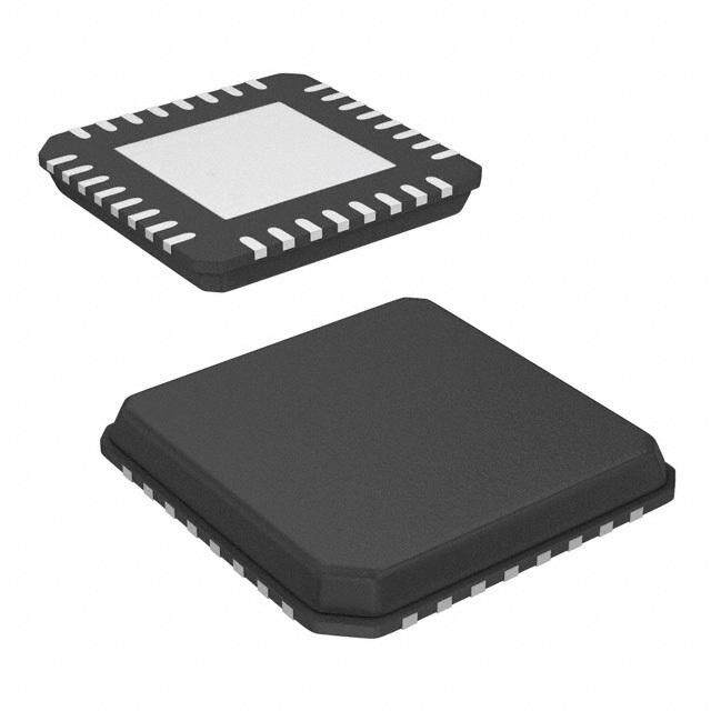
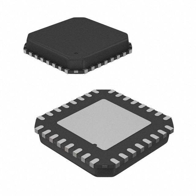
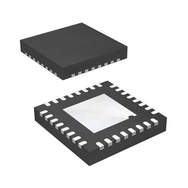
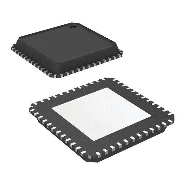
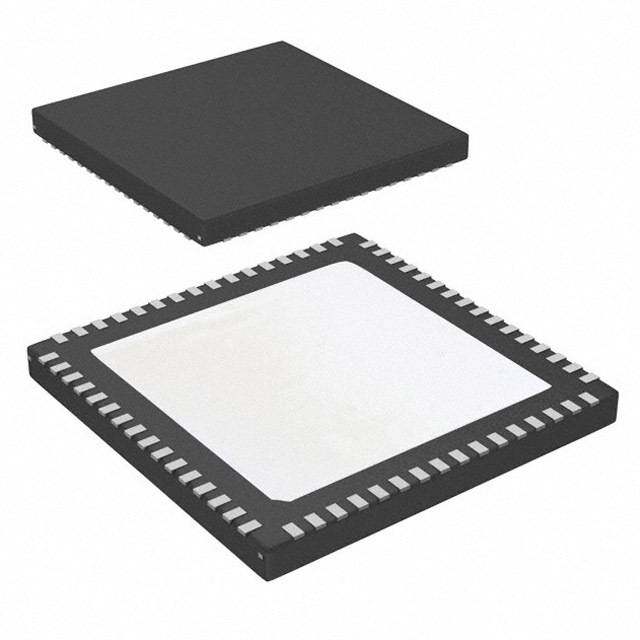
| 封装/外壳 | 40-VFQFN 裸露焊盘 |
| 封装/箱体 | QFN-40 |
| 工作温度 | 0°C ~ 70°C |
| 工作电源电压 | 1.8 V to 3.6 V |
| 工厂包装数量 | 490 |
| 应用 | 住宅/楼宇自动化,工业控制和监控 |
| 接收供电电流 | 18.4 mA |
| 数据接口 | PCB,表面贴装 |
| 数据速率(最大值) | 1Mbps |
| 最大工作温度 | + 125 C |
| 最大数据速率 | 1 Mbps |
| 最小工作温度 | - 55 C |
| 标准包装 | 490 |
| 灵敏度 | - 97 dBm |
| 电压-电源 | 1.8 V ~ 3.6 V |
| 电流-传输 | 21mA |
| 电流-接收 | 21mA |
| 类型 | CyFi |
| 系列 | CYRF7936 |
| 调制或协议 | DSSS,GFSK |
| 调制格式 | DSSS, GFSK |
| 输出功率 | 4 dBm |
| 频率 | 2.4GHz |
| 频率范围 | .4 GHz |


- 商务部:美国ITC正式对集成电路等产品启动337调查
- 曝三星4nm工艺存在良率问题 高通将骁龙8 Gen1或转产台积电
- 太阳诱电将投资9.5亿元在常州建新厂生产MLCC 预计2023年完工
- 英特尔发布欧洲新工厂建设计划 深化IDM 2.0 战略
- 台积电先进制程称霸业界 有大客户加持明年业绩稳了
- 达到5530亿美元!SIA预计今年全球半导体销售额将创下新高
- 英特尔拟将自动驾驶子公司Mobileye上市 估值或超500亿美元
- 三星加码芯片和SET,合并消费电子和移动部门,撤换高东真等 CEO
- 三星电子宣布重大人事变动 还合并消费电子和移动部门
- 海关总署:前11个月进口集成电路产品价值2.52万亿元 增长14.8%


PDF Datasheet 数据手册内容提取
CYRF7936 2.4 GHz CyFi™ Transceiver Features ■Operating voltage from 1.8V to 3.6V ■Operating temperature from 0°C to 70°C ■2.4-GHz direct sequence spread spectrum (DSSS) radio transceiver ■Space saving 40-pin QFN 6 × 6 mm package ■Operates in the unlicensed worldwide industrial, scientific, and Applications medical (ISM) band (2.400 GHz to 2.483 GHz) s ■21-mA operating current (transmit at –5 dBm) ■Wireless sensor networks n ■Transmit power up to +4 dBm ■Wireless actuator control g ■Receive sensitivity up to –97 dBm ■Home automation i s ■Sleep current less than 1 μA ■White goods e ■DSSS data rates up to 250 kbps, Gaussian frequency-shift ■Commercial building automation d keying (GFSK) data rate of 1 Mbps ■Automatic meter readers w ■Low external component count ■Precision agriculture e ■Auto transaction sequencer (ATS) - no MCU intervention ■Remote controls n ■Framing, length, CRC16, and auto acknowledge (ACK) ■Consumer electronics r ■Power management unit (PMU) for MCU ■Personal health and fitness o ■Fast startup and fast channel changes f ■Toys ■Separate 16 byte transmit and receive FIFOs d Applications Support e ■Dynamic data rate reception The CYRF7936 CyFi™ transceiver is a radio IC designed for low d ■Receive signal strength indication (RSSI) power embedded wireless applications. It can be used only with n ■Serial peripheral interface (SPI) control while in sleep mode Cypress’s PSoC programmable system-on-chip. Combined with e the PSoC and a CyFi network protocol stack, CYRF7936 can be ■4-MHz SPI microcontroller interface used to implement a complete CyFi wireless system. m ■Battery voltage monitoring circuitry Seewww.cypress.com for development tools, reference m designs, and application notes. ■Supports coin-cell operated applications o Logic Block Diagram c VREG VDD VCC PACTL e r L/D PMU V CyFi Radio Modem BAT GFSK RFP VIO Data Modulator RF DSSS N IRQ Interface Baseband RF SS# and BIAS SCK Sequencer & Framer MISO GFSK MOSI SPI Demodulator RSSI Xtal Osc Synthesizer RST XTAL XOUT GND CypressSemiconductorCorporation • 198 Champion Court • SanJose, CA 95134-1709 • 408-943-2600 Document Number: 001-48013 Rev. *I Revised May 19, 2017
CYRF7936 Contents Pinouts ..............................................................................3 Absolute Maximum Ratings ..........................................13 Pin Description .................................................................3 Operating Conditions .....................................................13 Functional Overview ........................................................4 DC Characteristics .........................................................13 Data Transmission Modes ...........................................4 AC Characteristics .........................................................14 Packet Framing ...........................................................4 RF Characteristics ..........................................................15 Packet Buffers .............................................................5 Typical Operating Characteristics ................................17 Auto Transaction Sequencer (ATS) ............................5 Ordering Information ......................................................19 Data Rates ..................................................................5 Ordering Code Definitions .........................................19 Functional Block Overview ..............................................6 Package Description ......................................................20 s 2.4-GHz CyFi Radio Modem .......................................6 Acronyms ........................................................................21 n Frequency Synthesizer ................................................6 Document Conventions .................................................21 g Baseband and Framer .................................................6 Units of Measure .......................................................21 i Packet Buffers and Radio Configuration Registers .....6 Document History Page .................................................22 s SPI Interface ................................................................6 Sales, Solutions, and Legal Information ......................23 e Interrupts .....................................................................8 Worldwide Sales and Design Support .......................23 d Clocks ..........................................................................8 Products ....................................................................23 Power Management ....................................................8 PSoC® Solutions ......................................................23 w Receiver Front End .....................................................8 Cypress Developer Community .................................23 Receive Spurious Response .......................................9 Technical Support .....................................................23 e Application Examples ......................................................9 n r o f d e d n e m m o c e r t o N Document Number: 001-48013 Rev. *I Page 2 of 23
CYRF7936 Pinouts Figure 1. Pin Diagram - CYRF7936 40-Pin QFN Ctaobrnser REGV NC BAT0V L/D NC DDV RST IOV NC NC 4 3 3 3 3 3 3 3 3 3 0 9 8 7 6 5 4 3 2 1 XTAL 1 30 PACTL / GPIO NC 2 29 XOUT / GPIO VCC 3 28 MISO / GPIO NC 4 CYRF7936 27 MOSI / SDAT s NC 5 CyFi Transciever 26 IRQ / GPIO n 40 lead QFN g VBAT1 6 25 SCK i VCC 7 24 SS s VBAT2 8 23 NC e NC 9 22 NC d * E-PAD Bottom Side RFBIAS 10 21 NC w 11 12 13 14 15 16 17 18 19 20 e R G R N N V N N R N PF ND NF C C CC C C ES C n V r Pin Description o f CYRF7936 40-Pin QFN d Pin Number Name Type Default Description e 1 XTAL I I 12-MHz crystal d 2, 4, 5, 9, 14, 15, NC NC Connect to GND n 17, 18, 20, 21, 22, e 23, 31, 32, 36, 39 m 3, 7, 16 V Pwr V = 2.4V to 3.6V. Typically connected to V . CC CC REG m 6, 8, 38 V Pwr V = 1.8V to 3.6V. Main supply. BAT(0-2) BAT 10 RFBIAS O O RF I/O 1.8V reference voltage o 11 RF I/O I Differential RF signal to and from antenna c P 12 GND GND Ground e 13 RF I/O I Differential RF signal to and from antenna r N 19 RESV I Must be connected to GND t o 24 SS# I I SPI enable, active LOW assertion. Enables and frames transfers. N 25 SCK I I SPI clock 26 IRQ I/O O Interrupt output (configurable active HIGH or LOW), or GPIO 27 MOSI I/O I SPI data input pin master out slave in (MOSI) or serial data (SDAT) 28 MISO I/O Z SPI data output pin - master in slave out (MISO), or GPIO (in SPI 3-pin mode). Tristates when SPI 3PIN = 0 and SS# is deasserted. 29 XOUT I/O O Buffered 0.75, 1.5, 3, 6, or 12 MHz clock, PACTL, or GPIO. Tristates in sleep mode (configure as GPIO drive LOW). 30 PACTL I/O O Control signal for external PA, T/R switch, or GPIO 33 V Pwr I/O interface voltage, 1.8V to 3.6V IO 34 RST I I Device reset. Internal 10-k(cid:58) pull-down resistor. Active HIGH, typically connect through a 0.47-(cid:80)F capacitor to V Must have RST=1 event the first time power BAT. is applied to the radio. Otherwise, the radio control register state is unknown. Document Number: 001-48013 Rev. *I Page 3 of 23
CYRF7936 Pin Description (continued) CYRF7936 40-Pin QFN Pin Number Name Type Default Description 35 V Pwr Decoupling pin for 1.8V logic regulator, connect through a 0.47-(cid:80)F capacitor to DD GND. 37 LVD O PMU inductor or diode connection, when used. If not used, connect to GND. 40 V Pwr PMU boosted output voltage feedback REG E-pad GND GND Must be soldered to ground s Corner tabs NC NC Do not solder the tabs and keep other signal traces clear. All tabs are common to n the lead frame or paddle, which is grounded after the pad is grounded. While they g are visible to the user, they do not extend to the bottom. i s Functional Overview Both 64 chip and 32 chip pseudo noise (PN) codes are supported e in 8DR mode. In general, lower data rates reduce packet error d The CYRF7936 IC is designed to implement wireless device rate in any given environment. links operating in the worldwide 2.4-GHz ISM frequency band. It Packet Framing w is intended for systems compliant with worldwide regulations covered by ETSI EN 301 489-1 V1.41, ETSI EN 300 328-1 The CYRF7936 IC device supports the following data packet e V1.3.1 (Europe), FCC CFR 47 Part 15 (USA and Industry framing features: n Canada), and TELEC ARIB_T66_March, 2003 (Japan). SOP The CYRF7936 contains a 2.4-GHz CyFi radio modem, which r features a 1-Mbps GFSK radio front-end, packet data buffering, Packets begin with a two-symbol SOP marker. The o packet framer, DSSS baseband controller, and RSSI. SOP_CODE_ADR PN code used for the SOP is different from f CYRF7936 features a SPI interface for data transfer and device that used for the “body” of the packet, and if necessary may be d configuration. a different length. SOP must be configured to be the same length on both sides of the link. e The CyFi radio modem supports 98 discrete 1-MHz channels (regulations may limit the use of some of these channels in d Length certain jurisdictions). n This is the first eight bits after the SOP symbol and is transmitted The baseband performs DSSS spreading and despreading, at the payload data rate. An EOP condition is inferred after e start-of-packet (SOP), end-of-packet (EOP) detection, and reception of the number of bytes defined in the length field, plus m CRC16 generation and checking. The baseband may also be two bytes for the CRC16. configured to automatically transmit ACK handshake packets m whenever a valid packet is received. CRC16 When in receive mode, with packet framing enabled, the device The device may be configured to append a 16-bit CRC16 to each o is always ready to receive data transmitted at any of the packet. The CRC16 uses the USB CRC polynomial with the c supported bit rates. This enables the implementation of added programmability of the seed. If enabled, the receiver e mixed-rate systems in which different devices use different data verifies the calculated CRC16 for the payload data against the rates. This also enables the implementation of dynamic data rate received value in the CRC16 field. The seed value for the CRC16 r systems that use high data rates at shorter distances or in a calculation is configurable, and the CRC16 transmitted may be t low-moderate interference environment or both. It changes to calculated using either the loaded seed value or a zero seed. The o lower data rates at longer distances or in high interference received data CRC16 is checked against both the configured N environments or both. and zero CRC16 seeds. In addition, the CYRF7936 IC has a power management unit CRC16 detects the following errors: (PMU), which allows direct connection of the device to any battery voltage in the range 1.8V to 3.6V. The PMU conditions ■Any one bit in error. the battery voltage to provide the supply voltages required by the ■Any two bits in error (irrespective of how far apart, which device, and may supply external devices. column, and so on). Data Transmission Modes ■Any odd number of bits in error (irrespective of the location). The CyFi radio transceiver supports two different data ■An error burst as wide as the checksum itself. transmission modes: Figure2 shows an example packet with SOP, CRC16, and ■In GFSK mode, data is transmitted at 1 Mbps, without any lengths fields enabled and Figure3 shows a standard ACK DSSS. packet. ■In 8DR mode, DSSS is enabled and eight bits are encoded in each derived code symbol transmitted. Document Number: 001-48013 Rev. *I Page 4 of 23
CYRF7936 Figure 2. Example Packet Format Preamble 2nd Framing n x 16us Symbol* P SOP 1 SOP 2 Length Payload Data CRC 16 Packet 1st Framing Symbol* length s 1 Byte *Note:32 or 64us Period n g Figure 3. Example ACK Packet Format i Preamble 2nd Framing s n x 16us Symbol* e P SOP 1 SOP 2 CRC 16 d 1st Framing CRC field from w Symbol* received packet. *Note:32 or 64us 2 Byte periods e Packet Buffers Similarly, when receiving in transaction mode, the device n automatically: All data transmission and reception use the 16-byte packet buffers: one for transmission and one for reception. ■Waits in receive mode for a valid packet to be received r o The transmit buffer allows loading a complete packet of up to ■Transitions to transmit mode, transmits an ACK packet 16bytes of payload data in one burst SPI transaction. This is f then transmitted with no further MCU intervention. Similarly, the ■Transitions to the transaction end state (receive mode to await d receive buffer allows receiving an entire packet of payload data the next packet, and so on.) e up to 16 bytes with no firmware intervention required until the The contents of the packet buffers are not affected by the packet reception is complete. d transmission or reception of ACK packets. Maximum packet length depends on the accuracy of the clock on n In each case, the entire packet transaction takes place without each end of the link. Packet lengths up to 40 bytes are supported any need for MCU firmware action (as long as packets of 16 e when the delta between the transmitter and receiver crystals is bytes or less are used). To transmit data, the MCU must load the m 60 ppm or better. Interrupts are provided to allow an MCU to use data packet to be transmitted, set the length, and set the TX GO the transmit and receive buffers as FIFOs. When transmitting a bit. Similarly, when receiving packets in transaction mode, m packet longer than 16 bytes, the MCU can load 16 bytes initially, firmware must retrieve the fully received packet in response to and add further bytes to the transmit buffer as transmission of an interrupt request indicating reception of a packet. o data creates space in the buffer. Similarly, when receiving packets longer than 16 bytes, the MCU must fetch received data Data Rates c from the FIFO periodically during packet reception to prevent it e The CYRF7936 IC supports the following data rates by from overflowing. combining the PN code lengths and data transmission modes r Auto Transaction Sequencer (ATS) described in the previous sections: t o The CYRF7936 IC provides automated support for transmission ■1000 kbps (GFSK) N and reception of acknowledged data packets. ■250 kbps (32 chip 8DR) When transmitting in transaction mode, the device automatically: ■125 kbps (64 chip 8DR) ■Starts the crystal and synthesizer ■Enters transmit mode ■Transmits the packet in the transmit buffer ■Transitions to receive mode and waits for an ACK packet ■Transitions to the transaction end state when an ACK packet is received or a timeout period expires Document Number: 001-48013 Rev. *I Page 5 of 23
CYRF7936 Functional Block Overview SPI communication is described as follows: ■Command direction (bit 7) = ‘1’ enables SPI write transaction. 2.4-GHz CyFi Radio Modem When it equals a ‘0’, it enables SPI read transactions. The CyFi radio modem is a dual conversion low IF architecture ■Command increment (bit 6) = ‘1’ enables SPI auto address optimized for power, range, and robustness. The CyFi radio increment. When set, the address field automatically modem employs channel-matched filters to achieve high increments at the end of each data byte in a burst access. performance in the presence of interference. An integrated Otherwise the same address is accessed. power amplifier (PA) provides up to +4 dBm transmit power, with an output power control range of 34 dB in seven steps. The ■Six bits of address supply current of the device is reduced as the RF output power is reduced. ■Eight bits of data s The device receives SCK from an application MCU on the SCK n Table 1. Internal PA Output Power Step Table pin. Data from the application MCU is shifted in on the MOSI pin. g PA Setting Typical Output Power (dBm) Data to the application MCU is shifted out on the MISO pin. The active LOW SS# pin must be asserted to initiate an SPI transfer. i 7 +4 s The application MCU can initiate SPI data transfers using a 6 0 e multibyte transaction. The first byte is the Command/Address 5 –5 byte and the following bytes are the data bytes as shown in d Table2 through Figure 6 on page 7. 4 –13 w 3 –18 The SPI communications interface has a burst mechanism, where the first byte can be followed by as many data bytes as e 2 –24 required. A burst transaction is terminated by deasserting the n 1 –30 slave select (SS# = 1). 0 –35 The SPI communications interface single read and burst read r sequences are shown in Figure4 and Figure 5 on page 7, o respectively. f Frequency Synthesizer The SPI communications interface single write and burst write d sequences are shown in Figure6 and Figure 7 on page 7, Prior to transmission or reception, the frequency synthesizer e respectively. must settle. The settling time varies depending on the channel; d 25 fast channels are provided with a maximum settling time of This interface may be optionally operated in a 3-pin mode with n 100 μs. the MISO and MOSI functions combined in a single bidirectional data pin (SDAT). When using the 3-pin mode, firmware must e The ‘fast channels’ (less than 100 μs settling time) are every third ensure that the MOSI pin on the MCU is in a high-impedance channel, starting at 0 up to and including 72 (for example, 0, 3, m state except when MOSI is actively transmitting data. 6, 9 …. 69, 72). The device registers may be written to or read from one byte at m Baseband and Framer a time, or several sequential register locations may be written or The baseband and framer blocks provide the DSSS encoding read in a single SPI transaction using incrementing burst mode. o and decoding, SOP generation and reception, CRC16 In addition to single byte configuration registers, the device c generation and checking, and EOP detection and length field. includes register files. Register files are FIFOs written to and e read from using nonincrementing burst SPI transactions. Packet Buffers and Radio Configuration Registers r The IRQ pin function may be optionally multiplexed to the MOSI Packet data and configuration registers are accessed through pin. When this option is enabled, the IRQ function is not available t o the SPI interface. All configuration registers are directly while the SS# pin is LOW. When using this configuration, addressed through the address field in the SPI packet. firmware must ensure that the MOSI pin on the MCU is in a high N Configuration registers allow configuration of DSSS PN codes, impedance state whenever the SS# pin is HIGH. data rate, operating mode, interrupt masks, interrupt status, and The SPI interface is not dependent on the internal 12 MHz clock. so on. Registers may therefore be read from or written to when the device is in sleep mode, and the 12 MHz oscillator disabled. SPI Interface The SPI interface and the IRQ and RST pins have a separate The CYRF7936 IC has an SPI interface supporting voltage reference pin (V ). This enables the device to interface communication between an application MCU and one or more IO directly to MCUs operating at voltages below the CYRF7936 IC slave devices (including the CYRF7936). The SPI interface supply voltage. supports single-byte and multi-byte serial transfers using either 4-pin or 3-pin interfacing. The SPI communications interface consists of slave select (SS#), serial clock (SCK), MOSI, MISO, or SDAT. Document Number: 001-48013 Rev. *I Page 6 of 23
CYRF7936 Table 2. SPI Transaction Format Parameter Byte 1 Byte 1+N Bit # 7 6 [5:0] [7:0] Bit Name DIR INC Address Data Figure 4. SPI Single Read Sequence SCK s SS n cmd addr g MOSI DIR INC A5 A4 A3 A2 A1 A0 0 i data to mcu s MISO D7 D6 D5 D4 D3 D2 D1 D0 e d Figure 5. SPI Incrementing Burst Read Sequence w e SCK n SS r o cmd addr MOSI DIR INC A5 A4 A3 A2 A1 A0 f 0 data to mcu1 data to mcu1+N d MISO D7 D6 D5 D4 D3 D2 D1 D0 D7 D6 D5 D4 D3 D2 D1 D0 e d n Figure 6. SPI Single Write Sequence e m SCK m SS o cmd addr data from mcu MOSI DIR INC A5 A4 A3 A2 A1 A0 D7 D6 D5 D4 D3 D2 D1 D0 c 1 e MISO r Figure 7. SPI Incrementing Burst Write Sequence SCK SS cmd addr data from mcu1 data from mcu1+N MOSI DIR INC A5 A4 A3 A2 A1 A0 D7 D6 D5 D4 D3 D2 D1 D0 D7 D6 D5 D4 D3 D2 D1 D0 1 MISO Document Number: 001-48013 Rev. *I Page 7 of 23
CYRF7936 Interrupts The output voltage (V ) of the PMU is configurable to several REG minimum values between 2.4V and 2.7V. V may be used to The device provides an interrupt (IRQ) output, which is REG provide up to 15 mA (average load) to external devices. It is configurable to indicate the occurrence of different events. The possible to disable the PMU and provide an externally regulated IRQ pin can be programmed to be either active HIGH or active DC supply voltage to the device’s main supply in the range 2.4V LOW; it can be a CMOS or open drain output. to 3.6V. The PMU also provides a regulated 1.8V supply to the The CYRF7936 IC features three sets of interrupts: transmit, logic. receive, and system interrupts. These interrupts all share a The PMU is designed to provide high boost efficiency (74%–85% single pin (IRQ), but can be independently enabled or disabled. depending on input voltage, output voltage, and load) when The contents of the enable registers are preserved when using a Schottky diode and power inductor. This eliminates the switching between transmit and receive modes. need for an external boost converter in many systems where s If more than one interrupt is enabled at any time, it is necessary other components require a boosted voltage. However, to read the relevant status register to determine which event reasonable efficiencies (69%–82% depending on input voltage, n caused the IRQ pin to assert. Even when a given interrupt source output voltage, and load) can be achieved when using low cost g is disabled, the status of the condition that otherwise causes an components such as SOT23 diodes and 0805 inductors. i interrupt can be determined by reading the appropriate status s The current through the diode must stay within the linear register. It is therefore possible to use devices without the IRQ operating range of the diode. For some loads the SOT23 diode e pin, by polling the status registers to wait for an event, rather than is sufficient, but with higher loads it is not; a SS12 diode must be d using the IRQ pin. used to stay within this linear range of operation. Along with the Clocks diode, the inductor used must not saturate its core. In higher w loads, a lower resistance/higher saturation coil such as the A 12-MHz crystal (30 ppm or better) is directly connected inductor from Sumida must be used. e between XTAL and GND without the need for external The PMU also provides a configurable low battery detection n capacitors. A digital clock out function is provided, with selectable output frequencies of 0.75, 1.5, 3, 6, or 12 MHz. This function, which can be read over the SPI interface. One of seven thresholds between 1.8V and 2.7V can be selected. The r output may be used to clock an external microcontroller (MCU) o interrupt pin can be configured to assert when the voltage on the or ASIC. This output is enabled by default, but may be disabled. V pin falls below the configured threshold. LV IRQ is not a f BAT The requirements to directly connect the crystal to the XTAL pin latched event. Battery monitoring is disabled when the device is d and GND are: in sleep mode. e ■Nominal frequency: 12 MHz Receiver Front End d ■Operating mode: Fundamental mode The gain of the receiver can be controlled directly by writing to n ■Resonance mode: Parallel resonant the low-noise amplifier (LNA) bit and the attenation (ATT) bit of e the RX_CFG_ADR register. Clearing the LNA bit reduces the ■Frequency stability: ±30 ppm receiver gain approximately 20 dB, allowing accurate reception m of very strong received signals (for example, when operating a ■Series resistance: <60 (cid:58) m receiver very close to the transmitter). Approximately 30 dB of ■Load capacitance: 10 pF receiver attenuation can be added by setting the ATT bit. This o limits data reception to devices at very short ranges. Enabling ■Drive level: 100 μW LNA is recommended, unless receiving from a device using c external PA. e Power Management When the device is in receive mode, the RSSI_ADR register r The operating voltage of the device is 1.8V to 3.6V DC, which returns the relative signal strength of the on-channel signal is applied to the V pin. The device can be shut down to a fully t BAT power. o static sleep mode by writing to the FRCEND=1 and ENDSTATE=000 bits in the XACT_CFG_ADR register over the When receiving, the device automatically measures and stores N SPI interface. The device enters sleep mode within 35 μs after the relative strength of the signal being received as a five bit the last SCK positive edge at the end of this SPI transaction. value. An RSSI reading is taken automatically when the SOP is Alternatively, the device may be configured to automatically detected. In addition, a new RSSI reading is taken every time the enter sleep mode after completing the packet transmission or previous reading is read from the RSSI_ADR register. This reception. When in sleep mode, the on-chip oscillator is stopped, allows the background RF energy level on any given channel to but the SPI interface remains functional. The device wakes from be easily measured when RSSI is read while no signal is being sleep mode automatically when the device is commanded to received. A new reading can occur as fast as once every 12 μs. enter transmit or receive mode. When resuming from sleep mode, there is a short delay while the oscillator restarts. The device can be configured to assert the IRQ pin when the oscillator has stabilized. Document Number: 001-48013 Rev. *I Page 8 of 23
CYRF7936 Receive Spurious Response The workaround for this is to program an additional byte in the The transmitter may exhibit spurs around 50MHz offset at levels packet header which contains the transmitter channel number. approximately 50dB to 60dB below the carrier power. Receivers After the packet is received, the channel number can be operating at the transmit spur frequency may receive the spur if checked. If the channel number does not match the receive the spur level power is greater than the receive sensitivity level. channel then the packet is rejected. Application Examples Figure 8. Recommended Circuit for Systems where V (cid:100)2.4V BAT s n g i s e d w e n r o f d CYRF7936 de n e m m o c e r t o N Document Number: 001-48013 Rev. *I Page 9 of 23
CYRF7936 Table 3. Recommended BoM for Systems where V (cid:100) 2.4V BAT Item Qty CY Part Number Reference Description Manufacturer Mfr Part Number 1 1 NA ANT1 2.5 GHz H-STUB Wiggle Antenna for 32 NA NA MIL PCB 2 1 730-10012 C1 CAP 15 PF 50 V CERAMIC NPO 0402 Panasonic ECJ-0EC1H150J 3 1 730-11955 C3 CAP 2.0 PF 50 V CERAMIC NPO 0402 Kemet C0402C209C5GACTU 4 1 730-11398 C4 CAP 1.5PF 50 V CERAMIC NPO 0402 PANASONIC ECJ-0EC1H1R5C SMD s 5 1 730R-13322 C5 CAP CER.47 uF 6.3 V X5R 0402 Murata GRM155R60J474KE1 n 9D g 6 2 730-13037 C12,C7 CAP CERAMIC 10 uF 6.3 V X5R 0805 Kemet C0805C106K9PACTU i 7 1 730-13400 C8 CAP 1 uF 6.3 V CERAMIC X5R 0402 Panasonic ECJ-0EB0J105M s e 8 6 730-13404 C9,C10,C11, CAP 0.047 uF 50 V CERAMIC X5R AVX 0402YD473KAT2A C13,C15,C16 0402 d 9 1 730R-11952 C17 CAP.10UF 10 V CERAMIC X5R 0402 Kemet C0402C104K8PACTU w 10 1 800-13317 D1 Diode Schottky 0.5A 40 V SOT23 DIODES INC BAT400D-7-F e 11 1 420-11976 J1 CONN HEADER 12 PIN 2MM GOLD Hirose Electric DF11-12DP-2DSA(01) Co. Ltd. n 12 1 800-13401 L1 INDUCTOR 22NH 2% FIXED 0603 Panasonic - ECG ELJ-RE22NGF2 r SMD o 13 1 800-11651 L2 INDUCTOR 1.8NH +-.3NH FIXED 0402 Panasonic - ECG ELJ-RF1N8DF f SMD d 14 1 800-10594 L3 COIL 10UH 1100MA CHOKE 0805 Newark 30K5421 e 15 1 630-11356 R1 RES 1.00 OHM 1/8W 1% 0805 SMD Yageo 9C08052A1R00FKHFT d 16 1 610-13402 R2 RES 47 OHM 1/16W 5% 0402 SMD Panasonic - ECG ERJ-2GEJ470X n 17 1 CYRF7936-40LFXC U1 IC, LP 2.4 GHz Radio SoC QFN-40 Cypress CYRF7936-40LFXC e Semiconductor m 18 1 800-13259 Y1 Crystal 12.00 MHZ HC49 SMD eCERA GF-1200008 19 1 PDCR-9515 REV01 PCB Printed Circuit Board Cypress PDCR-9515 REV01 m Semiconductor o 20 1 920-11206 LABEL1 Serial Number c 21 1 920-51500 REV01 LABEL2 PCA # 121R-51500 REV01 e r t o N Document Number: 001-48013 Rev. *I Page 10 of 23
CYRF7936 Figure 9. Recommended Circuit for Systems where V is 2.4V to 3.6V (PMU Disabled) BAT ANT1WIGGLE 32 12 C4 1.5 pFd 0402 C1 204015 pFd C320402.0 pFd Y1 12 MHz Crystal IND0603 L122 nH IND0402L21.8 nH PACTLTP2 CLKOUTTV1 C110.047 uFd gns C5 20400.47 uFd6053137433 GO312DCCCDIEVCCCRVVVVV10RFbias11RFp13RFn 30PACTL 1XTAL 29XOUT 19RESV20NC921NC1022NC1123NC1231NC1332NC1436NC1539NC16D1ADPN-GE 1241 C8C9C100.047 uFd0.047 uFd0.047 uFd040204020402 wdesi VCC 8863 210TTTAAABBBVVV RST SSSCKMOSIMISO IRQ L/D NC1NC2NC3NC4NC5NC6NC7NC8 C70.047 uFd0402 ne U1VCCCYRF7936 C170.47 uFd0402 RST34 LP_nSS24SCK25MOSI27MISOTP428 LP_IRQTP326 37 245914151718 VCC C60.047 uFd04020402 for d e d n e RST m SW1P0_1TP1 nLED1 nLED2 R3 0402NO LOAD m C1220401500 pFd 45P0_054P0_146P0_253P0_347P0_452P0_540P0_651P0_7 40P2_02P2_142P2_21P2_343P2_456P2_5 co CCV 5V 9224U2DDV 21DM20DP R10R11100040210025P1_0040218P1_1LP_nSSR625P1_2LP_IRQ1K17P1_30402R5SCK22P1_4MISO1K16P1_50402CLKOUT28P1_6R7MOSI15P1_71K0402 SSSSVVCY8C24794-24LFXI9051 RED = USB ACTIVITYGREEN = RF ACTIVITY5VD1 R8620nLED113GRKG0402R9620nLED224RDKR0402LED Green Red 5V S1SW11A2A1B2B SW PUSHBUTTON Power Supply VCC U315VINVOUT C1434DPYBASSENNG2.2 uFd0805TPS79133C1520.01 uFd0402 Not re 242406030603 R1R2 C13 4.7 uFd 5V 5V 0805 VBUSDMDP R4zero 2040 J11VBUS2DM3DP4GND5S16S2USB A RA PLUG Document Number: 001-48013 Rev. *I Page 11 of 23
CYRF7936 Table 4. Recommended BoM for Systems where V is 2.4 V - 3.6 V (PMU disabled) BAT Item Qty CY Part Number Reference Description Manufacturer Mfr Part Number 1 1 NA ANT1 2.5 GHz H-STUB Wiggle Antenna for 32MIL NA NA PCB 2 1 730-10012 C1 CAP 15 PF 50 V CERAMIC NPO 0402 Panasonic ECJ-0EC1H150J 3 1 730-11955 C3 CAP 2.0 PF 50 V CERAMIC NPO 0402 Kemet C0402C209C5GACTU 4 1 730-11398 C4 CAP 1.5 PF 50 V CERAMIC NPO 0402 SMD PANASONIC ECJ-0EC1H1R5C 5 1 730-13322 C5 CAP 0.47 uF 6.3 V CERAMIC X5R 0402 Murata GRM155R60J474KE19D 6 6 730-13404 C6,C7,C8,C CAP 0.047 uF 16 V CERAMIC X5R 0402 AVX 0402YD473KAT2A s 9,C10, C11 n 7 1 730-11953 C12 CAP 1500PF 50V CERAMIC X7R 0402 Kemet C0402C152K5RACTU g 8 1 730-13040 C13 CAP CERAMIC 4.7UF 6.3V XR5 0805 Kemet C0805C475K9PACTU i 9 1 730-12003 C14 CAP CER 2.2 uF 10 V 10% X7R 0805 Murata GRM21BR71A225KA01L s Electronics North e America d 10 1 800-13333 D1 LED GREEN/RED BICOLOR 1210 SMD LITEON LTST-C155KGJRKT 11 1 420-13046 J1 CONN USB PLUG TYPE A PCB SMT ACON UAR72-4N5J10 w 12 1 800-13401 L1 INDUCTOR 22NH 2% FIXED 0603 SMD Panasonic - ECG ELJ-RE22NGF2 e 13 1 800-11651 L2 INDUCTOR 1.8NH +-.3NH FIXED 0402 Panasonic - ECG ELJ-RF1N8DF n SMD 14 2 610-10037 R1, R2 RES 24 OHM 1/16W 5% 0603 SMD Panasonic - ECG ERJ-3GEYJ240V r o 15 1 610-10343 R4 RES ZERO OHM 1/16W 0402 SMD Panasonic - ECG ERJ-2GE0R00X f 16 3 610-10016 R5, R6, R7 RES CHIP 1K OHM 1/16W 5% 0402 SMD Panasonic - ECG ERJ-2GEJ102X d 17 2 610-13472 R9,R8 RES CHIP 620 OHM 1/16W 5% 0402 SMD Panasonic - ECG ERJ-2GEJ621X e 18 2 610-10684 R10, R11 RES CHIP 100 OHM 1/16W 5% 0402 SMD Phycomp USA Inc 9C1A04021000FLHF3 d 19 1 200-13471 S1 SWITCH LT 3.5MMX2.9MM 160GF SMD Panasonic - ECG EVQ-P7J01K n 20 1 CYRF7936-40LFC U1 IC, 2.4 GHz CyFi Transceiver QFN-40 Cypress CYRF7936 Rev A5 Semiconductor e 21 1 CY8C24794-24LFXI U2 PSoC Mixed Signal Array Cypress CY8C24794-24LFXI m Semiconductor m 22 1 800-13259 Y1 Crystal 12.00 MHZ HC49 SMD eCERA GF-1200008 23 1 LABEL1 Serial Number XXXXXX o c e r t o N Document Number: 001-48013 Rev. *I Page 12 of 23
CYRF7936 Absolute Maximum Ratings Static discharge voltage (digital)[9]............................>2000V Static discharge voltage (RF)[9]................................. 1100V Exceeding maximum ratings may shorten the useful life of the device. User guidelines are not tested. Latch-up current......................................+200 mA, –200 mA Storage temperature.................................–65°C to +150°C Operating Conditions Ambient temperature with power applied.–55°C to +125°C V ...................................................................2.4V to 3.6V CC Supply voltage on any power supply pin V ....................................................................1.8V to 3.6V IO relative to V ...............................................–0.3V to +3.9V SS V ..................................................................1.8V to 3.6V DC voltage to logic inputs[8]...................–0.3V to V +0.3V BAT IO T (ambient temperature under bias).............0°C to +70°C A DC voltage applied to outputs Ground voltage.................................................................0V in high-Z state........................................–0.3V to V +0.3V s IO F (crystal frequency).......................12 MHz ±30 ppm b OSC n DC Characteristics g (T = 25 (cid:113)C, V = 2.4 V, PMU disabled, f = 12.000000 MHz) BAT OSC i s Parameter Description Conditions Min Typ Max Unit e V Battery voltage 0 °C to 70 °C 1.8 – 3.6 V BAT V [10] PMU output voltage 2.4V mode 2.4 2.43 – V d REG VREG[10] PMU output voltage 2.7V mode 2.7 2.73 – V w V [11] V voltage 1.8 – 3.6 V IO IO e VCC VCCvoltage 0 °C to 70 °C 2.4[12] – 3.6 V n V Output high voltage condition 1 At I = –100.0 μA V – 0.2 V – V OH1 OH IO IO VOH2 Output high voltage condition 2 At IOH = –2.0 mA VIO – 0.4 VIO – V r o V Output low voltage At I = 2.0 mA – 0 0.45 V OL OL f V Input high voltage 0.7V – V V IH IO IO V Input low voltage 0 – 0.3V V d IL IO I Input leakage current 0 < V < V –1 0.26 +1 μA e IL IN IO C Pin input capacitance Except XTAL, RF , RF , RF – 3.5 10 pF d IN N P BIAS ICC (GFSK)[13] Average TX ICC, 1 Mbps, slow channel PA = 5, 2 way, 4 bytes/10 ms – 0.87 – mA n ICC (32-8DR)[13] Average TX ICC, 250 kbps, fast channel PA = 5, 2 way, 4 bytes/10 ms – 1.2 – mA e ISB[14] Sleep mode ICC – 0.8 10 μA m ISB[14] Sleep mode ICC PMU enabled – 31.4 – μA m IDLE I Radio off, XTAL Active XOUT disabled – 1.0 – mA CC I I during synth start – 8.4 – mA o synth CC TX I I during transmit PA = 5 (–5 dBm) – 20.8 – mA c CC CC TX I I during transmit PA = 6 (0 dBm) – 26.2 – mA e CC CC TX I I during transmit PA = 7 (+4 dBm) – 34.1 – mA r CC CC RX I I during receive LNA off, ATT on – 18.4 – mA t CC CC o RX I I during receive LNA on, ATT off – 21.2 – mA CC CC N Boost Eff PMU boost converter efficiency V = 2.5V, V = 2.73V, – 81 – % BAT REG I = 20 mA LOAD I [15] Average PMU external load current V = 1.8V, V = 2.73V, – – 15 mA LOAD_EXT BAT REG 0–50°C, RX mode I [15] Average PMU external load current V = 1.8V, V = 2.73V, 50 °C–70 °C, – – 10 mA LOAD_EXT BAT REG RX mode Notes 8. It is permissible to connect voltages above VIO to inputs through a series resistor limiting input current to 1 mA. AC timing not guaranteed. 9. Human body model (HBM). 10.VREGdepends on battery input voltage. 11.In sleep mode, the I/O interface voltage reference is VBAT. 12.In sleep mode, VCC min. can be as low as 1.8V. 13.Includes current drawn while starting crystal, starting synthesizer, transmitting packet (including SOP and CRC16), changing to receive mode, and receiving ACK handshake. Device is in sleep except during this transaction. 14.ISB is not guaranteed if any I/O pin is connected to voltages higher than VIO. 15.ILOAD_EXT is dependant on external components and this entry applies when the components connected to L/D are SS12 series diode and DH53100LC inductor from Sumida. Document Number: 001-48013 Rev. *I Page 13 of 23
CYRF7936 AC Characteristics Table 5. SPI Interface[16, 17] Parameter Description Min Typ Max Unit t SPI clock period 238.1 – – ns SCK_CYC t SPI clock high time 100 – – ns SCK_HI t SPI clock low time 100 – – ns SCK_LO t SPI input data setup time 25 – – ns DAT_SU t SPI input data hold time 10 – – ns s DAT_HLD n t SPI output data valid time 0 – 50 ns DAT_VAL g t SPI output data tristate (MOSI from slave select deassert) – 20 ns DAT_VAL_TRI i t SPI slave select setup time before first positive edge of SCK[18] 10 – – ns s SS_SU e t SPI slave select hold time after last negative edge of SCK 10 – – ns SS_HLD d t SPI slave select minimum pulse width 20 – – ns SS_PW t SPI slave select setup time 10 – – ns w SCK_SU tSCK_HLD SPI SCK hold time 10 – – ns e tRESET Minimum RST pin pulse width 10 – – ns n r Figure 10. SPI Timing o f tSCK_CYC d e SCK tSCK_HI tSCK_LO tSCK_HLD d t SCK_SU n nSS tSS_SU tSS_HLD e t t m DAT_SU DAT_HLD MOSI input m tDAT_VAL tDAT_VAL_TRI o MISO c e MOSI output r t o N Notes 16.AC values are not guaranteed if voltage on any pin exceeding VIO. 17.CLOAD = 30 pF 18.SCK must start low at the time SS# goes LOW, otherwise the success of SPI transactions are not guaranteed. Document Number: 001-48013 Rev. *I Page 14 of 23
CYRF7936 RF Characteristics Table 6. Radio Parameters Parameter Description Conditions Min Typ Max Unit RF frequency range Refer Note 19 2.400 – 2.497 GHz Receiver (T = 25°C, VCC = 3.0V, fOSC = 12.000000 MHz, BER < 1E-3) Sensitivity 125 kbps 64-8DR BER 1E-3 –97 – dBm Sensitivity 250 kbps 32-8DR BER 1E-3 –93 – dBm Sensitivity CER 1E-3 –80 –87 – dBm s Sensitivity GFSK BER 1E-3, ALL SLOW = 1 –84 – dBm n LNA gain – 22.8 – dB g ATT gain – –31.7 – dB i s Maximum received signal LNA On –15 –6 – dBm e RSSI value for PWR –60 dBm[20] LNA On 21 – Count in d RSSI slope 1.9 – dB/Count w Interference Performance(CER 1E-3) Co-channel Interference rejection C = –60 dBm – 9 – dB e carrier-to-Interference (C/I) n Adjacent (±1 MHz) channel selectivity C/I 1 MHz C = –60 dBm – 3 – dB r Adjacent (±2 MHz) channel selectivity C/I 2 MHz C = –60 dBm – –30 – dB o Adjacent (> 3 MHz) channel selectivity C/I > 3 MHz C = –67 dBm – –38 – dB f Out-of-band blocking 30 MHz–12.75 MHz[21] C = –67 dBm – –30 – dBm d Intermodulation C = –64 dBm, (cid:39)f = 5,10 MHz – –36 – dBm e Receive Spurious Emission d 800 MHz 100 kHz ResBW – –79 – dBm n 1.6 GHz 100 kHz ResBW – –71 – dBm e 3.2 GHz 100 kHz ResBW – –65 – dBm m Transmitter(T = 25°C, VCC = 3.0 V) m Maximum RF transmit power PA = 7 +2 4 +6 dBm o Maximum RF transmit power PA = 6 –2 0 +2 dBm c Maximum RF transmit power PA = 5 –7 –5 –3 dBm e Maximum RF transmit power PA = 0 – –35 – dBm r RF power control range – 39 – dB t RF power range control step size Seven steps, monotonic – 5.6 – dB o Frequency deviation min PN code pattern 10101010 – 270 – kHz N Frequency deviation max PN code pattern 11110000 – 323 – kHz Error vector magnitude (FSK error) >0 dBm – 10 – %rms Occupied bandwidth –6 dBc, 100 kHz ResBW 500 876 – kHz Transmit Spurious Emission (PA = 7) In-band spurious second channel power (±2 MHz) – –38 – dBm In-band spurious third channel power (>3 MHz) – –44 – dBm Notes 19.Subject to regulation. 20.RSSI value is not guaranteed. Extensive variation from part to part. 21.Exceptions F/3 and 5C/3. Document Number: 001-48013 Rev. *I Page 15 of 23
CYRF7936 Table 6. Radio Parameters (continued) Parameter Description Conditions Min Typ Max Unit Non harmonically related spurs (800 MHz) – –38 – dBm Non harmonically related spurs (1.6 GHz) – –34 – dBm Non harmonically related spurs (3.2 GHz) – –47 – dBm Harmonic spurs (second harmonic) – –43 – dBm Harmonic spurs (third harmonic) – –48 – dBm Fourth and greater harmonics – –59 – dBm s Power Management (Crystal PN# eCERA GF-1200008) n Crystal start to 10 ppm – 0.7 1.3 ms g Crystal start to IRQ XSIRQ EN = 1 – 0.6 – ms i Synth settle Slow channels – – 270 μs s e Synth settle Medium channels – – 180 μs d Synth settle Fast channels – – 100 μs Link turnaround time GFSK – – 30 μs w Link turnaround time 250 kbps – – 62 μs e Link turnaround time 125 kbps – – 94 μs n Link turnaround time <125 kbps – – 31 μs r Maximum packet length <60 ppm crystal-to-crystal – – 40 bytes o f d e d n e m m o c e r t o N Document Number: 001-48013 Rev. *I Page 16 of 23
CYRF7936 Typical Operating Characteristics The typical operating characteristics of CYRF7936 follow[22] Transmit Power vs. Temperature Transmit Power vs. Vcc Transmit Power vs. Channel (Vcc = 2.7v) (PMU off) 6 46 PA7 46 PA7 4 PA7 Output Power (dBm) ------1102864220 PPPAAA465 Output Power (dBm) ------1102864220 PPPAAA465 Output Power (dBm) ------1102864220 PPPAAA456 ns -14 -14 -14 g 0 20 40 60 2.4 2.6 2.8 3 3.2 3.4 3.6 0 20 40 60 80 Temp (deg C) Vcc Channel si e Typical RSSI Count vs Input Power Average RSSI vs. Temperature Average RSSI vs. Vcc (Rx signal = -70dBm) (Rx signal = -70dBm) d 32 19 20 19 w 18 18 24 17 17 e RSSI Count 16 LNA ONLNA OFFLANTAT OOFNF RSSI Count 111456 RSSI Count 11113456 r n 8 12 o 13 11 0 12 10 f -120 -100 -80 -60 -40 -20 0 20 40 60 2.4 2.6 2.8 3 3.2 3.4 3.6 Input Power (dBm) Temp (deg C) Vcc d e (RRxS SsIi gvnsa.l C=h a-n7n0delBm) Rx Sen(s1iMtbipvsi tCyE Rv)s. Vcc Rx Sensiti(v1iMtbyp sv sC.E RT)emperature d n 18 -80 -80 RSSI Count 1111024680246 Receiver Sensitivity (dBm) -------99988884208642 8DCRE3R2 Receiver Sensitivity (dBm) -------99988884208642 8DCRE3R2 comme 0 20 40 60 80 2.4 2.6 2.8 3 3.2 3.4 3.6 0 20 40 60 e Channel Vcc Temp (deg C) r Receiver Sensitivity vs. Frequency Offset Receiver Sensitivity vs Channel Carrier to Interferer t (3.0v, Room Temp) (Narrow band, LP modulation) o -80 -81 -82 GFSK 20.0 N Receiver Sensitivity (dBm)-------99998886420864 8DGRF6S4K Receiver Sensitivity (dBm)------998888319753 C8EDRR32 C/I (dB) -----1543210000000.......0000000 -60.0 -98 -95 -10 -5 0 5 10 -150 -100 -50 0 50 100 150 0 10 20 30 40 50 60 70 80 Channel Offset (MHz) Crystal Offset (ppm) Channel Note 22.With LNA on, ATT off, above –2dBm erroneous RSSI values may be read. Cross-checking RSSI with LNA off/on is recommended for accurate readings. Document Number: 001-48013 Rev. *I Page 17 of 23
CYRF7936 Typical Operating Characteristics (continued) BER vs. Data Threshold (32-8DR) GFSK vs. BER (SOP Threshold = 5, C38 slow) (SOP Threshold = 5, C38 slow) 10 100 0 Thru 7 1 10 1 0.1 %BER 0.01 %BER 00..011 0.001 0.001 0.0001 0.0001 GFSK s 0.00001 0.00001 n -100 -95 -90 -85 -80 -75 -70 -100 -80 -60 -40 -20 0 Input Power (dBm) Input Power (dBm) g i s ICC RX ICC RX ICC RX SYNTH (LNA OFF) (LNA ON) e 21 25 9.2 OPERATING CURRENT (mA) 11127890112....8905555 3322....0374VVVV OPERATING CURRENT (mA)222220123422222.....0123455555 3322....0374VVVV OPERATING CURRENT (mA) 8888888889..........891234567891 3322....0374VVVV newd 19.5 7.9 r 170 5 10 15 20 25 30 35 40 45 50 55 60 65 70 190 5 10 1520 25 30 35 40 45 5055 60 65 70 7.80 5 10 15 20 25 30 35 40 45 50 55 60 65 70 o TEMPERATURE (C) TEMPERATURE (C) TEMPERATURE (C) f d ICC TX SYNTH ICC TX @ PA0 ICC TX @ PA1 e 9.2 17 17.5 OPERATING CURRENT (mA) 8888888889..........891234567891 3322....0374VVVV OPERATING CURRENT (mA) 11145611...56555 3322....0374VVVV OPERATING CURRENT (mA) 111456111...567555 3322....0374VVVV mmend 7.9 7.8 14 14 o 0 5 10 15 20 25 30 35 40 45 50 55 60 65 70 0 5 10 15 20 25 30 3540 45 50 55 60 65 70 0 5 10 15 20 25 30 35 40 45 50 55 60 65 70 TEMPERATURE (C) TEMPERATURE (C) TEMPERATURE (C) c e ICC TX @ PA2 ICC TX @ PA3 ICC TX @ PA4 r 18 19 20.5 OPERATING CURRENT (mA) 11156711...67555 3322....0374VVVV OPERATING CURRENT (mA) 111678111...678555 3322....0374VVVV OPERATING CURRENT (mA) 1117891112...7890555 3322....0374VVVV 15 15.5 16.5 0 5 10 15 20 2530 35 4045 50 55 6065 70 0 5 10 15 20 2530 35 4045 50 55 6065 70 0 5 10152025303540455055606570 TEMPERATURE (C) TEMPERATURE (C) TEMPERATURE (C) Document Number: 001-48013 Rev. *I Page 18 of 23
CYRF7936 Typical Operating Characteristics (continued) ICC TX @ PA5 ICC TX @ PA6 ICC TX @ PA7 23.5 30 40.5 40 OPERATING CURRENT (mA)2220122222...0123555 3322....0374VVVV OPERATING CURRENT (mA) 222225678922222.....5678955555 3322....0374VVVV OPERATING CURRENT (mA) 333333334567893333333.......34567895555555 3322....0374VVVV s 19.50 5 10152025303540455055606570 24.50 5 10152025303540455055606570 32.50 5 10152025303540455055606570 n TEMPERATURE (C) TEMPERATURE (C) TEMPERATURE (C) g i s Figure 11. AC Test Loads and Waveforms for Digital Pins e d AC Test Loads DC Test Load w OUTPUT OUTPUT R1 V CC e 30 pF 5 pF OUTPUT n INCLUDING INCLUDING R2 JSICGO APNED Max JSICGO APNED Typical r o ALL INPUT PULSES f Parameter Unit VCC 90% 90% d R1 1071 (cid:58) 10% 10% R2 937 (cid:58) GND e Fall time: 1 V/ns d RTH 500 (cid:58) Rise time: 1 V/ns V 1.4 V n TH V 3.00 V Equivalent to: THÉVENIN EQUIVALENT e CC R TH OUTPUT VTH m m Ordering Information o Part Number Radio Package Name Package Type Operating Range c CYRF7936-40LTXC Transceiver 40-QFN 40-QFN (Sawn type) Commercial e Ordering Code Definitions r t CYRF 7936 40-LTX C o N Temperature range: = Commercial 40-pin QFN package X = Pb-free Part Number Marketing Code Company ID: CY = Cypress Document Number: 001-48013 Rev. *I Page 19 of 23
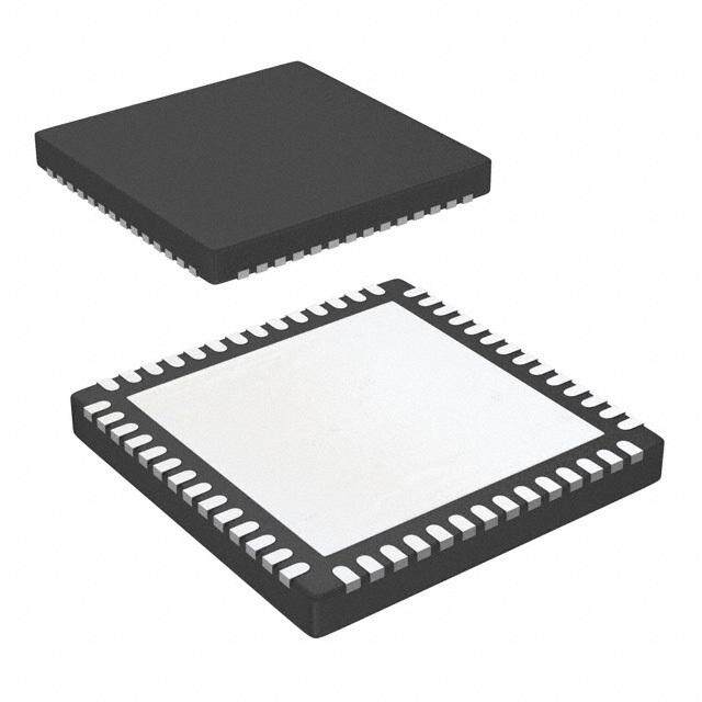
CYRF7936 Package Diagram The recommended dimension of the PCB pad size for the E-pad underneath the QFN is 3.5 mm × 3.5 mm (width × length). Figure 12. 40-Pin QFN (6 × 6 × 0.90 mm) Sawn Package Outline s n g i s e d w e n r o f d e d 001-44328 *G n e m m o c e r t o N Document Number: 001-48013 Rev. *I Page 20 of 23
CYRF7936 Acronyms Document Conventions Table 7. Acronyms Used in this Document Units of Measure Acronym Description Table 8. Units of Measure ACK acknowledge (packet received, no errors) Symbol Unit of Measure ATS auto transaction sequencer °C degree Celsius BER bit error rate dB decibels BOM bill of materials dBc decibel relative to carrier CMOS complementary metal oxide semiconductor dBm decibel-milliwatt s n CRC cyclic redundancy check Hz hertz g KB kilobyte, 1024 bytes DSSS direct sequence spread spectrum i Kbit kilobit, 1024 bits s EOP end-of-packet kHz kilohertz e FEC forward error correction k(cid:58) kilohms d GFSK gaussian frequency-shift keying MHz megahertz w HBM human body model M(cid:58) megaohm ISM industrial, scientific, and medical e (cid:80)A microamperes IRQ interrupt request n (cid:80)s microseconds LNA low-noise amplifier (cid:80)V microvolts r o MCU microcontroller unit (cid:80)Vrms microvolts root-mean-square f MISO master in slave out (cid:80)W microwatts d MOSI master out slave in mA milliampere e PA power amplifier ms millisecond d PLL phase locked loop mV millivolts n PMU power management unit nA nanoampere e PN pseudo noise ns nanosecond m nV nanovolts QFN quad flat no-leads m (cid:58) ohm RSSI received signal strength indication pp peak-to-peak o RF radio frequency ppm parts per million c Rx receive ps picosecond e SCK serial clock r sps samples per second SDAT serial data V volts t o SOP start-of-packet N SPI serial peripheral interface Tx transmit Document Number: 001-48013 Rev. *I Page 21 of 23
CYRF7936 Document History Page Description Title: CYRF7936, 2.4 GHz CyFi™ Transceiver Document Number: 001-48013 Orig. of Submission Revision ECN Description of Change Change Date ** 2557501 KKU / 08/25/2008 New data sheet AESA *A 2615458 KKU / 01/13/2009 Updated block diagram, changed SoP to SOP, changed EoP to EOP, changed AESA Frequency Initial Stability to Frequency Stability, change section on Low Noise Amplifier. to Receiver Front End and removed AGC enable. Updated Register s Map Summary. n *B 2672793 DPT / 03/12/2009 Updated packaging and ordering information. g PYRS i s *C 2902376 TGE 03/31/2010 Removed inactive parts from Ordering Information. Updated Package Diagram. e *D 2927979 TGE / 05/05/2010 Added Contents d AESA Removed Register Descriptions section. Updated links in Sales, Solutions, and Legal Information. w *E 3028381 TGE 09/13/2010 Updated Applications Support. e Added Ordering Code Definitions. Added Acronyms and Units of Measure. n *F 3346285 TGE 08/18/2011 Added “Receive Spurious Response” on page9. r Added footnote 20 on page 16. o Updated to new template. f *G 3611344 TGE 05/08/2012 Updated Package Diagram: spec 001-44328 – Changed revision from *D to *F. d *H 4525927 ANKC 10/06/2014 Updated to new template. e Completing Sunset Review. d *I 5742845 SGUP 05/19/2017 Added watermark “Not recommended for new designs” across the document. n Updated Package Diagram: spec 001-44328 – Changed revision from *F to *G. e Updated to new template. m m o c e r t o N Document Number: 001-48013 Rev. *I Page 22 of 23
CYRF7936 Sales, Solutions, and Legal Information Worldwide Sales and Design Support Cypress maintains a worldwide network of offices, solution centers, manufacturer’s representatives, and distributors. To find the office closest to you, visit us at Cypress Locations. Products PSoC® Solutions ARM® Cortex® Microcontrollers cypress.com/arm PSoC 1 |PSoC 3 |PSoC 4 | PSoC 5LP Automotive cypress.com/automotive Cypress Developer Community Clocks & Buffers cypress.com/clocks Forums | WICED IOT Forums |Projects | Video | Blogs | s Interface cypress.com/interface Training | Components n Internet of Things cypress.com/iot Technical Support g Memory cypress.com/memory i cypress.com/support s Microcontrollers cypress.com/mcu e PSoC cypress.com/psoc d Power Management ICs cypress.com/pmic w Touch Sensing cypress.com/touch USB Controllers cypress.com/usb e Wireless Connectivity cypress.com/wireless n r o f d e d n e m m o c e r © Cypress Semiconductor Corporation, 2007–2017. This document is the property of Cypress Semiconductor Corporation and its subsidiaries, including Spansion LLC ("Cypress"). This document, t including any software or firmware included or referenced in this document ("Software"), is owned by Cypress under the intellectual property laws and treaties of the United States and other countries o worldwide. Cypress reserves all rights under such laws and treaties and does not, except as specifically stated in this paragraph, grant any license under its patents, copyrights, trademarks, or other intellectual property rights. If the Software is not accompanied by a license agreement and you do not otherwise have a written agreement with Cypress governing the use of the Software, then Cypress N hereby grants you a personal, non-exclusive, nontransferable license (without the right to sublicense) (1) under its copyright rights in the Software (a) for Software provided in source code form, to modify and reproduce the Software solely for use with Cypress hardware products, only internally within your organization, and (b) to distribute the Software in binary code form externally to end users (either directly or indirectly through resellers and distributors), solely for use on Cypress hardware product units, and (2) under those claims of Cypress's patents that are infringed by the Software (as provided by Cypress, unmodified) to make, use, distribute, and import the Software solely for use with Cypress hardware products. Any other use, reproduction, modification, translation, or compilation of the Software is prohibited. TO THE EXTENT PERMITTED BY APPLICABLE LAW, CYPRESS MAKES NO WARRANTY OF ANY KIND, EXPRESS OR IMPLIED, WITH REGARD TO THIS DOCUMENT OR ANY SOFTWARE OR ACCOMPANYING HARDWARE, INCLUDING, BUT NOT LIMITED TO, THE IMPLIED WARRANTIES OF MERCHANTABILITY AND FITNESS FOR A PARTICULAR PURPOSE. To the extent permitted by applicable law, Cypress reserves the right to make changes to this document without further notice. Cypress does not assume any liability arising out of the application or use of any product or circuit described in this document. Any information provided in this document, including any sample design information or programming code, is provided only for reference purposes. It is the responsibility of the user of this document to properly design, program, and test the functionality and safety of any application made of this information and any resulting product. Cypress products are not designed, intended, or authorized for use as critical components in systems designed or intended for the operation of weapons, weapons systems, nuclear installations, life-support devices or systems, other medical devices or systems (including resuscitation equipment and surgical implants), pollution control or hazardous substances management, or other uses where the failure of the device or system could cause personal injury, death, or property damage ("Unintended Uses"). A critical component is any component of a device or system whose failure to perform can be reasonably expected to cause the failure of the device or system, or to affect its safety or effectiveness. Cypress is not liable, in whole or in part, and you shall and hereby do release Cypress from any claim, damage, or other liability arising from or related to all Unintended Uses of Cypress products. You shall indemnify and hold Cypress harmless from and against all claims, costs, damages, and other liabilities, including claims for personal injury or death, arising from or related to any Unintended Uses of Cypress products. Cypress, the Cypress logo, Spansion, the Spansion logo, and combinations thereof, WICED, PSoC, CapSense, EZ-USB, F-RAM, and Traveo are trademarks or registered trademarks of Cypress in the United States and other countries. For a more complete list of Cypress trademarks, visit cypress.com. Other names and brands may be claimed as property of their respective owners. Document Number: 001-48013 Rev. *I Revised May 19, 2017 Page 23 of 23