ICGOO在线商城 > 射频/IF 和 RFID > RF 收发器 IC > ADF7023BCPZ
 Datasheet下载
- 型号: ADF7023BCPZ
- 制造商: Analog
- 库位|库存: xxxx|xxxx
- 要求:
| 数量阶梯 | 香港交货 | 国内含税 |
| +xxxx | $xxxx | ¥xxxx |
查看当月历史价格
查看今年历史价格
ADF7023BCPZ产品简介:
ICGOO电子元器件商城为您提供ADF7023BCPZ由Analog设计生产,在icgoo商城现货销售,并且可以通过原厂、代理商等渠道进行代购。 ADF7023BCPZ价格参考。AnalogADF7023BCPZ封装/规格:RF 收发器 IC, IC 射频 TxRx + MCU 通用 ISM < 1GHz 431MHz ~ 464MHz,862MHz ~ 928MHz 32-WFQFN 裸露焊盘,CSP。您可以下载ADF7023BCPZ参考资料、Datasheet数据手册功能说明书,资料中有ADF7023BCPZ 详细功能的应用电路图电压和使用方法及教程。
ADF7023BCPZ 是由 Analog Devices Inc. 生产的一款高性能 RF 收发器 IC,适用于多种无线通信应用场景。该芯片支持 410 MHz 至 480 MHz 的频段,广泛应用于低功耗、远距离的无线数据传输系统中。以下是其主要应用场景:

 1. 智能计量与能源管理
ADF7023BCPZ 常用于智能电表、水表和气表等设备中,实现远程抄表和监控功能。它能够通过无线网络将能耗数据传输到中央管理系统,帮助用户实时监控能源使用情况,并优化能源分配。该芯片的低功耗特性使其非常适合电池供电的计量设备,延长了设备的工作寿命。

 2. 工业自动化与物联网 (IoT)
在工业自动化领域,ADF7023BCPZ 可以用于无线传感器网络 (WSN),实现设备之间的数据通信。例如,它可以连接温度、湿度、压力等传感器,将采集到的数据发送到控制中心,进行实时监控和分析。此外,它还适用于工厂自动化、物流跟踪等场景,帮助提高生产效率和管理水平。

 3. 智能家居与楼宇自动化
该芯片可用于智能家居系统中的各种设备,如智能门锁、安防摄像头、烟雾报警器等。通过无线通信,这些设备可以与家庭网关或手机应用程序连接,实现远程控制和状态监测。ADF7023BCPZ 的高可靠性和低功耗特性使得它成为智能家居产品的理想选择。

 4. 农业与环境监测
在农业领域,ADF7023BCPZ 可以用于土壤湿度、气象条件等环境参数的监测。农民可以通过无线传感器网络实时获取农田信息,优化灌溉和施肥方案,提高农作物产量。此外,它还可以用于森林火灾预警、水质监测等环保应用,帮助保护自然环境。

 5. 医疗保健
在医疗领域,ADF7023BCPZ 可用于可穿戴设备和远程健康监测系统。例如,它可以帮助医生实时监控患者的生理参数(如心率、血压等),并通过无线网络将数据传输到医院或医疗机构,实现远程诊断和治疗。

总之,ADF7023BCPZ 凭借其优异的性能和灵活性,广泛应用于多个行业的无线通信系统中,为各类应用场景提供了可靠的通信解决方案。
| 参数 | 数值 |
| 产品目录 | |
| 描述 | IC TX FSK/GFSK ISM BAND 32LFCSP射频收发器 Hi Perf Lo Pwr ISM FSK/GFSK/MSK/GMSK |
| 产品分类 | RF 收发器集成电路 - IC |
| 品牌 | Analog Devices |
| 产品手册 | |
| 产品图片 |
|
| rohs | 符合RoHS无铅 / 符合限制有害物质指令(RoHS)规范要求 |
| 产品系列 | RF集成电路,射频收发器,Analog Devices ADF7023BCPZ- |
| mouser_ship_limit | 此产品可能需要其他文件才能从美国出口。 |
| 数据手册 | |
| 产品型号 | ADF7023BCPZ |
| PCN组件/产地 | |
| 产品种类 | 射频收发器 |
| 传输供电电流 | 13 mA |
| 功率-输出 | 13.5dBm |
| 包装 | 托盘 |
| 商标 | Analog Devices |
| 天线连接器 | PCB,表面贴装 |
| 存储容量 | - |
| 安装风格 | SMD/SMT |
| 封装 | Tray |
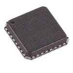
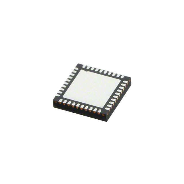
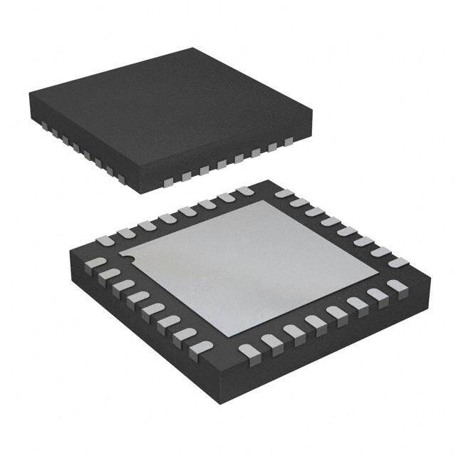
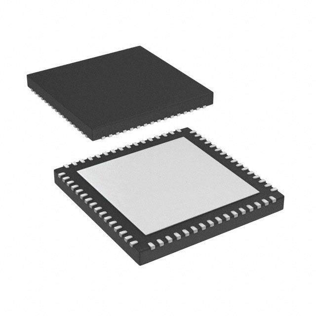
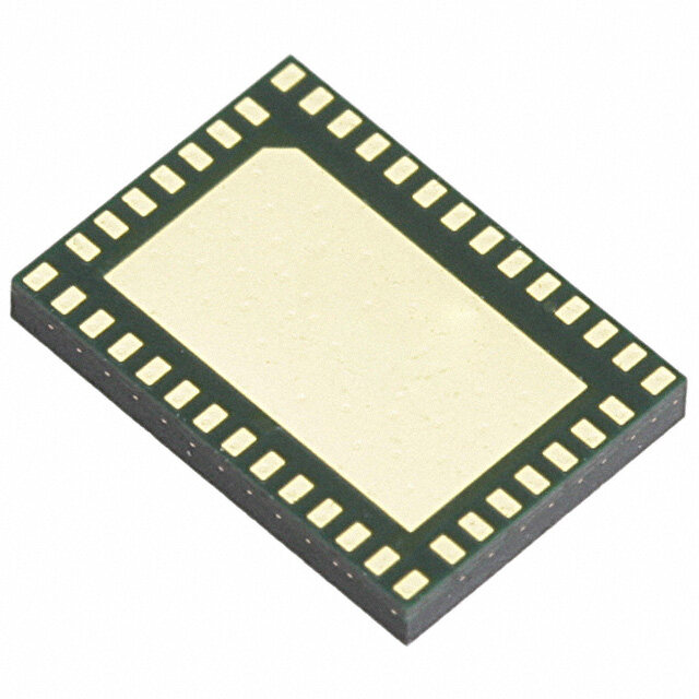
| 封装/外壳 | 32-WFQFN 裸露焊盘,CSP |
| 封装/箱体 | LFCSP-32 EP |
| 工作温度 | -40°C ~ 85°C |
| 工作电源电压 | 2.2 V to 3.6 V |
| 工厂包装数量 | 490 |
| 应用 | ISM |
| 接口类型 | 4-Wire SPI |
| 接收供电电流 | 12.8 mA |
| 数据接口 | PCB,表面贴装 |
| 数据速率(最大值) | 300kbps |
| 最大工作温度 | + 85 C |
| 最大数据速率 | 300 kbps |
| 最小工作温度 | - 40 C |
| 标准包装 | 1 |
| 灵敏度 | - 116 dBm |
| 电压-电源 | 2.2 V ~ 3.6 V |
| 电流-传输 | 32.1mA |
| 电流-接收 | 12.8mA |
| 电源电压-最大 | 3.6 V |
| 电源电压-最小 | 2.2 V |
| 类型 | ISM |
| 系列 | ADF7023 |
| 视频文件 | http://www.digikey.cn/classic/video.aspx?PlayerID=1364138032001&width=640&height=505&videoID=2245193150001 |
| 调制或协议 | FSK,GFSK,GMSK,MSK,OOK |
| 调制格式 | FSK, GFSK, GMSK, MSK, OOK |
| 输出功率 | - 16 dBm to + 13.5 dBm |
| 配用 | /product-detail/zh/EVAL-ADF7XXXMB4Z/EVAL-ADF7XXXMB4Z-ND/4866755 |
| 频率 | 431MHz ~ 464MHz,862MHz ~ 928MHz |
| 频率范围 | 862 MHz to 928 MHz |


_renders/CS4265-CNZR.jpg)

- 商务部:美国ITC正式对集成电路等产品启动337调查
- 曝三星4nm工艺存在良率问题 高通将骁龙8 Gen1或转产台积电
- 太阳诱电将投资9.5亿元在常州建新厂生产MLCC 预计2023年完工
- 英特尔发布欧洲新工厂建设计划 深化IDM 2.0 战略
- 台积电先进制程称霸业界 有大客户加持明年业绩稳了
- 达到5530亿美元!SIA预计今年全球半导体销售额将创下新高
- 英特尔拟将自动驾驶子公司Mobileye上市 估值或超500亿美元
- 三星加码芯片和SET,合并消费电子和移动部门,撤换高东真等 CEO
- 三星电子宣布重大人事变动 还合并消费电子和移动部门
- 海关总署:前11个月进口集成电路产品价值2.52万亿元 增长14.8%


PDF Datasheet 数据手册内容提取
High Performance, Low Power, ISM Band FSK/GFSK/OOK/MSK/GMSK Transceiver IC Data Sheet ADF7023 FEATURES Smart wake mode Current saving low power mode with autonomous receiver Ultralow power, high performance transceiver wake up, carrier sense, and packet reception Frequency bands Downloadable firmware modules 862 MHz to 928 MHz Image rejection calibration, fully automated (patent pending) 431 MHz to 464 MHz 128-bit AES encryption/decryption with hardware Data rates supported acceleration and key sizes of 128 bits, 192 bits, and 1 kbps to 300 kbps 256 bits 2.2 V to 3.6 V power supply Reed Solomon error correction with hardware acceleration Single-ended and differential PAs 240-byte packet buffer for TX/RX data Low IF receiver with programmable IF bandwidths Efficient SPI control interface with block read/write access 100 kHz, 150 kHz, 200 kHz, 300 kHz Integrated battery alarm and temperature sensor Receiver sensitivity (BER) Integrated RC and 32.768 kHz crystal oscillator −116 dBm at 1.0 kbps, 2FSK, GFSK On-chip, 8-bit ADC −107.5 dBm at 38.4 kbps, 2FSK, GFSK 5 mm × 5 mm, 32-pin, LFCSP package −102.5 dBm at 150 kbps, GFSK, GMSK −100 dBm at 300 kbps, GFSK, GMSK APPLICATIONS −104 dBm at 19.2 kbps, OOK Smart metering Very low power consumption IEEE 802.15.4g 12.8 mA in PHY_RX mode (maximum front-end gain) Wireless MBUS 24.1 mA in PHY_TX mode (10 dBm output, single-ended PA) Home automation 0.75 µA in PHY_SLEEP mode (32 kHz RC oscillator active) Process and building control 1.28 µA in PHY_SLEEP mode (32 kHz XTAL oscillator active) Wireless sensor networks (WSNs) 0.33 µA in PHY_SLEEP mode (Deep Sleep Mode 1) Wireless healthcare RF output power of −20 dBm to +13.5 dBm (single-ended PA) RF output power of −20 dBm to +10 dBm (differential PA) Patented fast settling automatic frequency control (AFC) Digital received signal strength indication (RSSI) Integrated PLL loop filter and Tx/Rx switch Fast automatic VCO calibration Automatic synthesizer bandwidth optimization On-chip, low-power, custom 8-bit processor Radio control Packet management Smart wake mode Packet management support Highly flexible for a wide range of packet formats Insertion/detection of preamble/sync word/CRC/address Manchester and 8b/10b data encoding and decoding Data whitening Rev. C Information furnished by Analog Devices is believed to be accurate and reliable. However, no responsibility is assumed by Analog Devices for its use, nor for any infringements of patents or other One Technology Way, P.O. Box 9106, Norwood, MA 02062-9106, U.S.A. rights of third parties that may result from its use. Specifications subject to change without notice. No license is granted by implication or otherwise under any patent or patent rights of Analog Devices. Tel: 781.329.4700 www.analog.com Trademarks and registered trademarks are the property of their respective owners. Fax: 781.461.3113 ©2010–2012 Analog Devices, Inc. All rights reserved.
ADF7023 Data Sheet TABLE OF CONTENTS Features .............................................................................................. 1 Interrupts in Sport Mode .......................................................... 53 Applications ....................................................................................... 1 ADF7023 Memory Map ................................................................ 54 Revision History ............................................................................... 3 BBRAM ........................................................................................ 54 Functional Block Diagram .............................................................. 4 Modem Configuration RAM (MCR) ...................................... 54 General Description ......................................................................... 4 Program ROM ............................................................................ 54 Specifications ..................................................................................... 6 Program RAM ............................................................................ 54 RF and Synthesizer Specifications .............................................. 6 Packet RAM ................................................................................ 55 Transmitter Specifications ........................................................... 7 SPI Interface .................................................................................... 56 Receiver Specifications ................................................................ 9 General Characteristics ............................................................. 56 Timing and Digital Specifications ............................................ 13 Command Access ....................................................................... 56 Auxilary Block Specifications ................................................... 14 Status Word ................................................................................. 56 General Specifications ............................................................... 15 Command Queuing ................................................................... 57 Timing Specifications ................................................................ 16 Memory Access ........................................................................... 58 Absolute Maximum Ratings .......................................................... 17 Low Power Modes .......................................................................... 61 ESD Caution ................................................................................ 17 Example Low Power Modes ...................................................... 64 Pin Configuration and Function Descriptions ........................... 18 Low Power Mode Timing Diagrams ........................................ 66 Typical Performance Characteristics ........................................... 20 WUC Setup ................................................................................. 67 Terminology .................................................................................... 32 Firmware Timer Setup ............................................................... 69 Radio Control .................................................................................. 33 Calibrating the RC Oscillator ................................................... 69 Radio States ................................................................................. 33 Downloadable Firmware Modules ............................................... 71 Initialization ................................................................................ 35 Writing a Module to Program RAM ........................................ 71 Commands .................................................................................. 35 Image Rejection Calibration Module ...................................... 71 Automatic State Transitions ...................................................... 37 Reed Solomon Coding Module ................................................ 71 State Transition and Command Timing .................................. 38 AES Encryption and Decryption Module............................... 71 Packet Mode .................................................................................... 43 Radio Blocks .................................................................................... 73 Preamble ...................................................................................... 43 Frequency Synthesizer ............................................................... 73 Sync Word ................................................................................... 44 Crystal Oscillator ........................................................................ 74 Payload ......................................................................................... 45 Modulation .................................................................................. 74 CRC .............................................................................................. 46 RF Output Stage.......................................................................... 74 Postamble..................................................................................... 47 PA/LNA Interface ....................................................................... 75 Transmit Packet Timing ............................................................ 47 Receive Channel Filter ............................................................... 75 Data Whitening .......................................................................... 48 Image Channel Rejection .......................................................... 75 Manchester Encoding ................................................................ 48 Automatic Gain Control (AGC) ............................................... 75 8b/10b Encoding ........................................................................ 48 RSSI .............................................................................................. 76 Sport Mode ...................................................................................... 49 2FSK/GFSK/MSK/GMSK Demodulation ............................... 78 Packet Structure in Sport Mode ............................................... 49 Clock Recovery ........................................................................... 80 Sport Mode in Transmit ............................................................ 49 OOK Demodulation .................................................................. 80 Sport Mode in Receive ............................................................... 49 Recommended Receiver Settings for Transmit Bit Latencies in Sport Mode ..................................... 49 2FSK/GFSK/MSK/GMSK ......................................................... 81 Interrupt Generation ...................................................................... 52 Recommended Receiver Settings for OOK ............................ 82 Rev. C | Page 2 of 112
Data Sheet ADF7023 Peripheral Features .......................................................................... 83 Host Processor Interface ............................................................ 85 Analog-to-Digital Converter ..................................................... 83 PA/LNA Matching ...................................................................... 85 Temperature Sensor .................................................................... 83 Command Reference ...................................................................... 87 Test DAC ...................................................................................... 83 Register Maps .................................................................................. 88 Transmit Test Modes .................................................................. 83 BBRAM Register Description ................................................... 90 Silicon Revision Readback ......................................................... 83 MCR Register Description ....................................................... 100 Applications Information ............................................................... 84 Outline Dimensions ...................................................................... 109 Application Circuit ..................................................................... 84 Ordering Guide ......................................................................... 109 REVISION HISTORY 7/12—Rev. B to Rev. C Added Figure 103; Renumbered Sequentially ............................. 70 Changes to Features Section ............................................................ 1 Changes to Writing a Module to Program RAM Section .......... 71 Changed 1.8 V to 2.2 V, General Description Section ................. 4 Changes to Automatic PA Ramp Section Equation and Image Changed 1.8 V to 2.2 V, Table 1 Summary .................................... 6 Channel Rejection Section ............................................................. 75 Changed 1.8 V to 2.2 V, Table 2 ....................................................... 7 Changes to Temperature Sensor Section and Table 43 .............. 83 Changes to Table 3 ............................................................................ 9 Changes to Figure 110 .................................................................... 84 Changes to Table 5 .......................................................................... 14 Changes to Figure 111 and Figure 112 ......................................... 85 Changes to V Parameter, Table 6 ............................................... 15 Changes to Support for External PA and LNA Control Section DD Changes to Timing Specifications Section ................................... 16 and Table 45 ..................................................................................... 86 Deleted t from Table 7, Figure 2, and Figure 3 ........................... 16 Changes to CMD_SYNC Description Column, Table 46.......... 87 1 Changes to Table 9 .......................................................................... 18 Changes to Table 48 ........................................................................ 88 Changes to Figure 5 to Figure 10 .................................................. 20 Changes to Table 49 ........................................................................ 89 Changes to Figure 11, Figure 12 Caption, Figure 13 and Changes to SYNTH_LUT_CONTROL_1 Description Column, Figure 14 Caption ............................................................................ 21 Table 70 ............................................................................................. 93 Changes to Figure 19 Caption to Figure 21 Caption .................. 22 Changes to Table 78 ........................................................................ 96 Changes to Figure 26 Caption ....................................................... 23 Changes to Table 79 ........................................................................ 97 Changes to Figure 34 Caption ....................................................... 24 Changes to Table 84 and Table 86 ................................................. 98 Changes to Figure 61 Caption and Figure 64 Caption ............... 29 Changes to Table 94 ........................................................................ 99 Changes to Figure 72 ...................................................................... 31 Added Table 95, Table 96, and Table 97; Renumbered Changes to PHY_SLEEP Section .................................................. 33 Sequentially .................................................................................... 100 Changes to Initialization After Application of Power Section, Changes to Table 101 .................................................................... 101 Initialization After Issuing the CMD_HW_RESET Command Added Table 124 and Table 125................................................... 105 Section, Initialization on Transitioning from PHY_SLEEP 3/11—Rev. A to Rev. B (After CS Is Brought Low) Section, and Initialization After a Changes to RSSI Method 3, Formula ........................................... 72 WUC Timeout Section ................................................................... 35 Changes to RSSI Method 4, Step 3 ................................................ 72 Changes to CMD_RAM_LOAD_DONE (0xC7) Section ......... 37 Changes to RSSI Method 4, Step 5 Formula and Formula Deleted CMD_SYNC (0xA2) Section .......................................... 37 Approximation ................................................................................ 73 Changes to State Transition and Command Timing Section .... 38 Added Register 0x361 to Table 49 .................................................8 5 Changes to Table 11 and Table 12 ................................................. 39 Added Table 129, Renumbered Subsequent Tables .................. 104 Changes to Addressing Section ..................................................... 45 Changes to Example Address Check Section, Table 18, and CRC 2/11—Rev. 0 to Rev. A Section .............................................................................................. 46 Changes to Table 9, DGUARD Description ................................ 18 Changes to Figure 79 ...................................................................... 47 Changes to Sport Mode in Receive Section ................................. 47 Changes to Figure 81 and Figure 82 ............................................. 50 Changes to Crystal Oscillator Section, Typical Crystal Load Changes to Figure 83 and Figure 84 ............................................. 51 Capacitance Tuning Range Value, and to Table 31 ..................... 70 Changes to CMD_FINISHED Description, Table 24................. 53 Changes to RSSI Method 3 Section .............................................. 72 Changes to Command Access Section ......................................... 56 Changes to RSSI Method 4 Section .............................................. 73 Changes to Figure 97 ...................................................................... 63 Changes to Table 41, 9.6 kbps and 1 kbps Data Rate Changes to Table 29 ........................................................................ 68 Setup Values ..................................................................................... 78 Added Calibrating the RC Oscillator Section, Performing a Fine Changes to Table 108, ADC_PD_N Description ...................... 100 Calibration of the RC Oscillator Section, and Performing a 8/10—Revision 0: Initial Version Coarse Calibration of the RC Oscillator Section ........................ 69 Rev. C | Page 3 of 112
ADF7023 Data Sheet FUNCTIONAL BLOCK DIAGRAM ADCIN_ATB3 FSK 4kB ROM CITRRQL IRQ_GP3 LNA ASK MAC RRFFIIOO__11NP LORGSASMI/P MUX 8A-BDICT DEMOD P8R-BOICTE RSISSOCR 2kB RAM MCSISO CDR SPI AFC 256 BYTE SCLK AGC PACKET PA RAM MOSI 64 BYTE BBRAM RFO2 PA DIVIDER FLILOTOEPR CHPUAMRGPE PFD 26MHz OSC 256 BYTE GPIO MCR RAM TEST DIVIDER DAC GPIO1 PA RAMP fDEV PROFILE ADF7023 Σ-Δ GAUSSIAN WAKE-UP CONTROL CLOCK MODULATOR FILTER TIMER UNIT DIVIDER 1 2 3 4 O O O O ANALOG TEMP BATTERY 32kHz 32kHz 26MHz LD LD LD LD BIAS TEST SENSOR MONITOR OSC RCOSC OSC 1GPIO REFECRRSE TGOR FPxINCSR 1E7G, V1C8,O 19C,R 2E0G, 2S5Y, NATNHD 2C7R.EGDIGx RBIAS XOSC32KN_ATB2 XOSC32KP_GP5_ATB1 XOSC26N XOSC26P 08291-001 Figure 1. GENERAL DESCRIPTION The ADF7023 is a very low power, high performance, highly A patent pending, image rejection calibration scheme is available integrated 2FSK/GFSK/OOK/MSK/GMSK transceiver designed through a program download. The algorithm does not require for operation in the 862 MHz to 928 MHz and 431 MHz to the use of an external RF source nor does it require any user 464 MHz frequency bands, which cover the worldwide license- intervention once initiated. The results of the calibration can be free ISM bands at 433 MHz, 868 MHz, and 915 MHz. It is suitable stored in nonvolatile memory for use on subsequent power-ups for circuit applications that operate under the European ETSI of the transceiver. EN300-220, the North American FCC (Part 15), the Chinese short- The ADF7023 operates with a power supply range of 2.2 V to range wireless regulatory standards, or other similar regional 3.6 V and has very low power consumption in both Tx and Rx standards. Data rates from 1 kbps to 300 kbps are supported. modes, enabling long lifetimes in battery-operated systems The transmit RF synthesizer contains a VCO and a low noise while maintaining excellent RF performance. The device can fractional-N PLL with an output channel frequency resolution enter a low power sleep mode in which the configuration of 400 Hz. The VCO operates at 2× or 4×, the fundamental settings are retained in BBRAM. frequency to reduce spurious emissions. The receive and transmit The ADF7023 features an ultralow power, on-chip, synthesizer bandwidths are automatically, and independently, communications processor. The communications processor, configured to achieve optimum phase noise, modulation quality, which is an 8-bit RISC processor, performs the radio control, and settling time. The transmitter output power is programmable packet management, and smart wake mode (SWM) functionality. from −20 dBm to +13.5 dBm, with automatic PA ramping to The communications processor eases the processing burden of meet transient spurious specifications. The part possesses both the companion processor by integrating the lower layers of a single-ended and differential PAs, which allows for Tx antenna typical communication protocol stack. The communications diversity. processor also permits the download and execution of a set of The receiver is exceptionally linear, achieving an IP3 specification firmware modules that include image rejection (IR) calibration, of −12.2 dBm and −11.5 dBm at maximum gain and minimum AES encryption, and Reed Solomon coding. gain, respectively, and an IP2 specification of 18.5 dBm and The communications processor provides a simple command-based 27 dBm at maximum gain and minimum gain, respectively. The radio control interface for the host processor. A single-byte receiver achieves an interference blocking specification of 66 dB command transitions the radio between states or performs a at ±2 MHz offset and 74 dB at ±10 MHz offset. Thus, the part is radio function. extremely resilient to the presence of interferers in spectrally noisy environments. The receiver features a novel, high speed, automatic frequency control (AFC) loop, allowing the PLL to find and correct any RF frequency errors in the recovered packet. Rev. C | Page 4 of 112
Data Sheet ADF7023 The communications processor provides support for generic These interrupt conditions can be configured to include the packet formats. The packet format is highly flexible and fully reception of valid preamble, sync word, CRC, or address match. programmable, thereby ensuring its compatibility with Wake-up from sleep mode can also be triggered by the host proprietary packet profiles. In transmit mode, the commun- processor. For systems requiring very accurate wake-up timing, ications processor can be configured to add preamble, sync a 32 kHz oscillator can be used to drive the wake-up timer. word, and CRC to the payload data stored in packet RAM. In Alternatively, the internal RC oscillator can be used, which gives receive mode, the communications processor can detect and lower current consumption in sleep. interrupt the host processor on reception of preamble, sync The ADF7023 features an advanced encryption standard (AES) word, address, and CRC and store the received payload to engine with hardware acceleration that provides 128-bit block packet RAM. The ADF7023 uses an efficient interrupt system encryption and decryption with key sizes of 128 bits, 192 bits, comprising MAC level interrupts and PHY level interrupts that and 256 bits. Both electronic code book (ECB) and Cipher can be individually set. The payload data plus the 16-bit CRC Block Chaining Mode 1 (CBC Mode 1) are supported. The AES can be encoded/decoded using Manchester or 8b/10b encoding. engine can be used to encrypt/decrypt packet data and can be Alternatively, data whitening and dewhitening can be applied. used as a standalone engine for encryption/decryption by the The smart wake mode (SWM) allows the ADF7023 to wake up host processor. The AES engine is enabled on the ADF7023 by autonomously from sleep using the internal wake-up timer downloading the AES software module to program RAM. The without intervention from the host processor. After wake-up, AES software module is available from Analog Devices, Inc. the ADF7023 is controlled by the communications processor. An on-chip, 8-bit ADC provides readback of an external analog This functionality allows carrier sense, packet sniffing, and input, the RSSI signal, or an integrated temperature sensor. An packet reception while the host processor is in sleep, thereby integrated battery voltage monitor raises an interrupt flag to the reducing overall system current consumption. The smart wake host processor whenever the battery voltage drops below a user- mode can wake the host processor on an interrupt condition. defined threshold. Rev. C | Page 5 of 112
ADF7023 Data Sheet SPECIFICATIONS V = VDDBAT1 = VDDBAT2 = 2.2 V to 3.6 V, GND = 0 V, T = T to T , unless otherwise noted. Typical specifications are at DD A MIN MAX V = 3 V, T = 25°C. DD A RF AND SYNTHESIZER SPECIFICATIONS Table 1. Parameter Min Typ Max Unit Test Conditions RF CHARACTERISTICS Frequency Ranges 862 928 MHz 431 464 MHz PHASE-LOCKED LOOP Channel Frequency Resolution 396.7 Hz Phase Noise (In-Band) −88 dBc/Hz 10 kHz offset, PA output power = 10 dBm, RF = 868 MHz Phase Noise at Offset of 1 MHz −126 dBc/Hz PA output power = 10 dBm, RF frequency = 868 MHz 2 MHz −131 dBc/Hz PA output power = 10 dBm, RF frequency = 868 MHz 10 MHz −142 dBc/Hz PA output power = 10 dBm, RF frequency = 868 MHz VCO Calibration Time 142 µs Synthesizer Settling Time 56 µs Frequency synthesizer settles to within ±5 ppm of the target frequency within this time following the VCO calibration, transmit, and receive, 2FSK/GFSK/MSK/GMSK CRYSTAL OSCILLATOR Crystal Frequency 26 MHz Parallel load resonant crystal Recommended Load Capacitance 7 18 pF Maximum Crystal ESR 1800 Ω 26 MHz crystal with 18 pF load capacitance Pin Capacitance 2.1 pF Capacitance for XOSC26P and XOSC26N Start-Up Time 310 µs 26 MHz crystal with 7 pF load capacitance 388 µs 26 MHz crystal with 18 pF load capacitance SPURIOUS EMISSIONS Integer Boundary Spurious 910.1 MHz −39 dBc Using 130 kHz synthesizer bandwidth, integer boundary spur at 910 MHz (26 MHz × 35), inside synthesizer loop bandwidth 911.0 MHz −79 dBc Using 130 kHz synthesizer bandwidth, integer boundary spur at 910 MHz (26 MHz × 35), outside synthesizer loop bandwidth Reference Spurious 868 MHz/915 MHz −80 dBc Using 130 kHz synthesizer bandwidth and using 92 kHz synthesizer bandwidth (default for PHY_RX) Clock-Related Spur Level −60 dBc Measured in a span of ±350 MHz for synthesizer bandwidth = 92 kHz, RF frequency = 868.95 MHz, PA output power = 10 dBm, V = 3.6 V, single-ended PA DD used Rev. C | Page 6 of 112
Data Sheet ADF7023 TRANSMITTER SPECIFICATIONS Table 2. Parameter Min Typ Max Unit Test Conditions DATA RATE 2FSK/GFSK/MSK/GMSK 1 300 kbps OOK 2.4 19.2 kbps Manchester encoding enabled (Manchester chip rate = 2 × data rate) Data Rate Resolution 100 bps MODULATION ERROR RATE (MER) RF frequency = 928 MHz, GFSK 10 kbps to 49.5 kbps 25.4 dB Modulation index = 1 49.6 kbps to 129.5 kbps 25.3 dB Modulation index = 1 129.6 kbps to 179.1 kbps 23.9 dB Modulation index = 0.5 179.2 kbps to 239.9 kbps 23.3 dB Modulation index = 0.5 240 kbps to 300 kbps 23 dB Modulation index = 0.5 MODULATION 2FSK/GFSK/MSK/GMSK Frequency 0.1 409.5 kHz Deviation Deviation Frequency Resolution 100 Hz Gaussian Filter BT 0.5 Nonprogrammable OOK PA Off Feedthrough −94 dBm VCO Frequency Pulling 30 kHz Data rate = 19.2 kbps (38.4 kcps Manchester rms encoded), PA output = 10 dBm, PA ramp rate = 64 codes/bit SINGLE-ENDED PA Maximum Power1 13.5 dBm Programmable, separate PA and LNA match2 Minimum Power −20 dBm Transmit Power Variation vs. ±0.5 dB From −40°C to +85°C, RF frequency = 868 MHz Temperature Transmit Power Variation vs. V ±1 dB From 2.2 V to 3.6 V, RF frequency = 868 MHz DD Transmit Power Flatness ±1 dB From 902 MHz to 928 MHz and 863 MHz to 870 MHz Programmable Step Size −20 dBm to +13.5 dBm 0.5 dB Programmable in 63 steps DIFFERENTIAL PA Maximum Power1 10 dBm Programmable Minimum Power −20 dBm Transmit Power Variation vs. ±1 dB From −40°C to +85°C, RF frequency = 868 MHz Temperature Transmit Power Variation vs. V ±2 dB From 2.2 V to 3.6 V, RF frequency = 868 MHz DD Transmit Power Flatness ±1 dB From 863 MHz to 870 MHz Programmable Step Size −20 dBm to +10 dBm 0.5 dB Programmable in 63 steps HARMONICS 868 MHz, unfiltered conductive, PA output power = 10 dBm Single-Ended PA Second Harmonic −15.1 dBc Third Harmonic −29.3 dBc All Other Harmonics −47.6 dBc Differential PA Second Harmonic −23.2 dBc Third Harmonic −25.2 dBc All Other Harmonics −24.2 dBc Rev. C | Page 7 of 112
ADF7023 Data Sheet Parameter Min Typ Max Unit Test Conditions OPTIMUM PA LOAD IMPEDANCE Single-Ended PA, in Transmit Mode f = 915 MHz 50.8 + j10.2 Ω RF f = 868 MHz 45.5 + j12.1 Ω RF f = 433 MHz 46.8 + j19.9 Ω RF Single-Ended PA, in Receive Mode f = 915 MHz 9.4 − j124 Ω RF f = 868 MHz 9.5 − j130.6 Ω RF f = 433 MHz 11.9 − j260.1 Ω RF Differential PA, in Transmit Mode Load impedance between RFIO_1P and RFIO_1N to ensure maximum output power f = 915 MHz 20.5 + j36.4 Ω RF f = 868 MHz 24.7 + j36.5 Ω RF f = 433 MHz 55.6 + j81.5 Ω RF 1 Measured as the maximum unmodulated power. 2 A combined single-ended PA and LNA match can reduce the maximum achievable output power by up to 1 dB. Rev. C | Page 8 of 112
Data Sheet ADF7023 RECEIVER SPECIFICATIONS Table 3. Parameter Min Typ Max Unit Test Conditions 2FSK/GFSK/MSK/GMSK INPUT At BER = 1E − 3, RF frequency = 433 MHz, 868 MHz, SENSITIVITY, BIT ERROR RATE (BER) 915 MHz, LNA and PA matched separately1 1.0 kbps −116 dBm Frequency deviation = 4.8 kHz, IF filter bandwidth = 100 kHz 10 kbps −111 dBm Frequency deviation = 9.6 kHz, IF filter bandwidth = 100 kHz 38.4 kbps −107.5 dBm Frequency deviation = 20 kHz, IF filter bandwidth = 100 kHz 50 kbps −106.5 dBm Frequency deviation = 12.5 kHz, IF filter bandwidth = 100 kHz 100 kbps −105 dBm Frequency deviation = 25 kHz, IF filter bandwidth = 100 kHz 150 kbps −104 dBm Frequency deviation = 37.5 kHz, IF filter bandwidth = 150 kHz 200 kbps −103 dBm Frequency deviation = 50 kHz, IF filter bandwidth = 200 kHz 300 kbps −100.5 dBm Frequency deviation = 75 kHz, IF filter bandwidth = 300 kHz 2FSK/GFSK/MSK/GMSK INPUT At PER = 1%, RF frequency = 433 MHz, 868 MHz, 915 MHz, SENSITIVITY, PACKET ERROR RATE (PER) LNA and PA matched separately1, packet length = 128 bits, packet mode 1.0 kbps −115.5 dBm Frequency deviation = 4.8 kHz, IF filter bandwidth = 100 kHz 9.6 kbps −110.6 dBm Frequency deviation = 9.6 kHz, IF filter bandwidth = 100 kHz 38.4 kbps −106 dBm Frequency deviation = 20 kHz, IF filter bandwidth = 100 kHz 50 kbps −104.3 dBm Frequency deviation = 12.5 kHz, IF filter bandwidth = 100 kHz 100 kbps −102.6 dBm Frequency deviation = 25 kHz, IF filter bandwidth = 100 kHz 150 kbps −101 dBm Frequency deviation = 37.5 kHz, IF filter bandwidth = 150 kHz 200 kbps −99.1 dBm Frequency deviation = 50 kHz, IF filter bandwidth = 200 kHz 300 kbps −97.9 dBm Frequency deviation = 75 kHz, IF filter bandwidth = 300 kHz OOK INPUT SENSITIVITY, PACKET ERROR At PER = 1%, RF frequency = 433 MHz, 868 MHz, 915 MHz, RATE (PER) LNA and PA matched separately1, packet length = 128 bits, packet mode, IF filter bandwidth = 100 kHz 19.2 kbps (38.4 kcps, Manchester −104.7 dBm Encoded) 2.4 kbps (4.8 kcps, Manchester −109.7 dBm Encoded) LNA AND MIXER, INPUT IP3 Receiver LO frequency (f ) = 914.8 MHz, f = f + LO SOURCE1 LO 0.4 MHz, f = f + 0.7 MHz SOURCE2 LO Minimum LNA Gain −11.5 dBm Maximum LNA Gain −12.2 dBm LNA AND MIXER, INPUT IP2 Receiver LO frequency (f ) = 920.8 MHz, f = f + LO SOURCE1 LO 1.1 MHz, f = f + 1.3 MHz SOURCE2 LO Max LNA Gain, Max Mixer Gain 18.5 dBm Min LNA Gain, Min Mixer Gain 27 dBm Rev. C | Page 9 of 112
ADF7023 Data Sheet Parameter Min Typ Max Unit Test Conditions LNA AND MIXER, 1 dB COMPRESSION RF frequency = 915 MHz POINT Max LNA Gain, Max Mixer Gain −21.9 dBm Min LNA Gain, Min Mixer Gain −21 dBm ADJACENT CHANNEL REJECTION CW Interferer Wanted signal 3 dB above the input sensitivity level (BER = 10−3), CW interferer power level increased until BER = 10−3, image calibrated 200 kHz Channel Spacing 38 dB IF BW = 100 kHz, wanted signal: F = 12.5 kHz, DEV DR = 50 kbps 300 kHz Channel Spacing 39 dB IF BW = 100 kHz, wanted signal: F = 25 kHz, DEV DR = 100 kbps 38 dB IF BW = 150 kHz, wanted signal: F = 37.5 kHz, DEV DR = 150 kbps 400 kHz Channel Spacing 40 dB IF BW = 200 kHz, wanted signal: F = 50 kHz, DEV DR = 200 kbps 600 kHz Channel Spacing 41 dB IF BW = 300 kHz, wanted signal: F = 75 kHz, DEV DR = 300 kbps Modulated Interferer Wanted signal 3 dB above the input sensitivity level (BER = 10−3), modulated interferer with the same modulation as the wanted signal; interferer power level increased until BER = 10−3, image calibrated 200 kHz Channel Spacing 38 dB IF BW = 100 kHz, wanted signal: F = 12.5 kHz, DEV DR = 50 kbps 300 kHz Channel Spacing 36 dB IF BW = 100 kHz, wanted signal: F = 25 kHz, DEV DR = 100 kbps 300 kHz Channel Spacing 36 dB IF BW = 150 kHz, wanted signal: F = 37.5 kHz, DEV DR = 150 kbps 400 kHz Channel Spacing 34 dB IF BW = 200 kHz, wanted signal: F = 50 kHz, DEV DR = 200 kbps 600 kHz Channel Spacing 35 dB IF BW = 300 kHz, wanted signal: F = 75 kHz, DEV DR = 300 kbps CO-CHANNEL REJECTION −4 dB Desired signal 10 dB above the input sensitivity level (BER = 10−3), data rate = 38.4 kbps, frequency deviation = 20 kHz, RF frequency = 868 MHz BLOCKING Desired signal 3 dB above the input sensitivity level (BER = 10−3) of −107.5 dBm (data rate = 38.4 kbps), modulated interferer power level increased until BER = 10−3 (see the Typical Performance Characteristics section for blocking at other offsets and IF bandwidths) RF Frequency = 433 MHz ±2 MHz 68 dB ±10 MHz 76 dB RF Frequency = 868 MHz ±2 MHz 66 dB ±10 MHz 74 dB RF Frequency = 915 MHz ±2 MHz 66 dB ±10 MHz 74 dB Rev. C | Page 10 of 112
Data Sheet ADF7023 Parameter Min Typ Max Unit Test Conditions BLOCKING, ETSI EN 300 220 Measurement procedure as per ETSI EN 300 220-1 V2.3.1; desired signal 3 dB above the ETSI EN 300 220 reference sensitivity level of −99 dBm, IF bandwidth = 100 kHz, data rate = 38.4 kbps, unmodulated interferer; see the Typical Performance Characteristics section for blocking at other offsets and IF bandwidths, RF frequency = 868 MHz ±2 MHz −28 dBm ±10 MHz −20.5 dBm WIDEBAND INTERFERENCE REJECTION 75 dB RF frequency = 868 MHz, swept from 10 MHz to 100 MHz either side of the RF frequency IMAGE CHANNEL ATTENUATION Measured as image attenuation at the IF filter output, carrier wave interferer at 400 kHz below the channel frequency, 100 kHz IF filter bandwidth 868 MHz, 915 MHz 36/45 dB Uncalibrated/calibrated 433 MHz 40/54 dB Uncalibrated/calibrated AFC Accuracy 1 kHz Maximum Pull-In Range Achievable pull-in range dependent on discriminator bandwidth and modulation 300 kHz IF Filter Bandwidth ±150 kHz 200 kHz IF Filter Bandwidth ±100 kHz 150 kHz IF Filter Bandwidth ±75 kHz 100 kHz IF Filter Bandwidth ±50 kHz PREAMBLE LENGTH Minimum number of preamble bits to ensure the minimum packet error rate across the full input power range AFC Off, AGC Lock on Sync Word Detection 38.4 kbps 8 Bits 300 kbps 24 Bits AFC On, AFC and AGC Lock on Preamble Detection 9.6 kbps 44 Bits 38.4 kbps 44 Bits 50 kbps 50 Bits 100 kbps 52 Bits 150 kbps 54 Bits 200 kbps 58 Bits 300 kbps 64 Bits AFC On, AFC and AGC Lock on Sync Word Detection 38.4 kbps 14 Bits 300 kbps 32 Bits RSSI Range at Input −97 to −26 dBm Linearity ±2 dB Absolute Accuracy ±3 dB SATURATION (MAXIMUM INPUT LEVEL) 2FSK/GFSK/MSK/GMSK 12 dBm OOK −13 dBm OOK modulation depth = 20 dB 10 dBm OOK modulation depth = 60 dB Rev. C | Page 11 of 112
ADF7023 Data Sheet Parameter Min Typ Max Unit Test Conditions LNA INPUT IMPEDANCE Receive Mode f = 915 MHz 75.9 − j32.3 Ω RF f = 868 MHz 78.0 − j32.4 Ω RF f = 433 MHz 95.5 − j23.9 Ω RF Transmit Mode f = 915 MHz 7.6 + j9.2 Ω RF f = 868 MHz 7.7 + j8.6 Ω RF f = 433 MHz 7.9 + j4.6 Ω RF RX SPURIOUS EMISSIONS2 Maximum <1 GHz −66 dBm At antenna input, unfiltered conductive Maximum >1 GHz −62 dBm At antenna input, unfiltered conductive 1 Sensitivity for combined matching network case is typically 1 dB less than separate matching networks. 2 Follow the matching and layout guidelines to achieve the relevant FCC/ETSI specifications. Rev. C | Page 12 of 112
ADF7023 TIMING AND DIGITAL SPECIFICATIONS Table 4. Parameter Min Typ Max Unit Test Conditions RX AND TX TIMING PARAMETERS See the State Transition and Command Timing section for more details PHY_ON to PHY_RX (on CMD_PHY_RX) 300 μs Includes VCO calibration and synthesizer settling PHY_ON to PHY_TX (on CMD_PHY_TX) 296 μs Includes VCO calibration and synthesizer settling, does not include PA ramp-up LOGIC INPUTS Input High Voltage, V 0.7 × V V INH DD Input Low Voltage, V 0.2 × V V INL DD Input Current, I /I ±1 µA INH INL Input Capacitance, C 10 pF IN LOGIC OUTPUTS Output High Voltage, V V − 0.4 V I = 500 µA OH DD OH Output Low Voltage, V 0.4 V I = 500 µA OL OL GPIO Rise/Fall 5 ns GPIO Load 10 pF Maximum Output Current 5 mA ATB OUTPUTS Used for external PA and LNA control ADCIN_ATB3 and ATB4 Output High Voltage, V 1.8 V OH Output Low Voltage, V 0.1 V OL Maximum Output Current 0.5 mA XOSC32KP_GP5_ATB1 and XOSC32KN_ATB2 Output High Voltage, V V V OH DD Output Low Voltage, V 0.1 V OL Maximum Output Current 5 mA Rev. C | Page 13 of 112
ADF7023 Data Sheet AUXILARY BLOCK SPECIFICATIONS Table 5. Parameter Min Typ Max Unit Test Conditions 32 kHz RC OSCILLATOR Frequency 32.768 kHz After calibration Frequency Accuracy 1.5 % After calibration at 25°C Frequency Drift Temperature Coefficient 0.14 %/°C Voltage Coefficient 4 %/V Calibration Time 1.25 ms 32 kHz XTAL OSCILLATOR Frequency 32.768 kHz Start-Up Time 630 ms 32.768 kHz crystal with 7 pF load capacitance WAKE UP CONTROLLER (WUC) Hardware Timer Wake-Up Period 61 × 10−6 1.31 × 10⁵ sec Firmware Timer Wake-Up Period 1 216 Hardware Firmware counter counts of the number of periods hardware wake-ups, resolution of 16 bits ADC Resolution 8 Bits DNL ±1 LSB V from 2.2 V to 3.6 V, T = 25°C DD A INL ±1 LSB V from 2.2 V to 3.6 V, T = 25°C DD A Conversion Time 1 µs Input Capacitance 12.4 pF BATTERY MONITOR Absolute Accuracy ±45 mV Alarm Voltage Set Point 1.7 2.7 V Alarm Voltage Step Size 62 mV 5-bit resolution Start-Up Time 100 µs Current Consumption 30 µA When enabled TEMPERATURE SENSOR Range −40 +85 °C Resolution 0.3 °C With averaging Accuracy of Temperature Readback +7/−4 °C Over temperature range −40°C to +85°C (calibrated at +25°C) Rev. C | Page 14 of 112
Data Sheet ADF7023 GENERAL SPECIFICATIONS Table 6. Parameter Min Typ Max Unit Test Conditions TEMPERATURE RANGE, T −40 +85 °C A VOLTAGE SUPPLY V 2.2 3.6 V Applied to VDDBAT1 and VDDBAT2 DD TRANSMIT CURRENT CONSUMPTION In the PHY_TX state, single-ended PA matched to 50 Ω, differential PA matched to 100 Ω, separate single-ended PA and LNA match, combined differential PA and LNA match Single-Ended PA, 433 MHz −10 dBm 8.7 mA 0 dBm 12.2 mA 10 dBm 23.3 mA 13.5 dBm 32.1 mA Differential PA, 433 MHz −10 dBm 7.9 mA 0 dBm 11 mA 5 dBm 15 mA 10 dBm 22.6 mA Single-Ended PA, 868 MHz/915 MHz −10 dBm 10.3 mA 0 dBm 13.3 mA 10 dBm 24.1 mA 13.5 dBm 32.1 mA Differential PA, 868 MHz/915 MHz −10 dBm 9.3 mA 0 dBm 12 mA 5 dBm 16.7 mA 10 dBm 28 mA POWER MODES PHY_SLEEP (Deep Sleep Mode 2) 0.18 µA Sleep mode, wake-up configuration values (BBRAM) not retained PHY_SLEEP (Deep Sleep Mode 1) 0.33 µA Sleep mode, wake-up configuration values (BBRAM) retained PHY_SLEEP (RCO Wake Mode) 0.75 µA WUC active, RC oscillator running, wake-up configuration values retained (BBRAM) PHY_SLEEP (XTO Wake Mode) 1.28 µA WUC active, 32 kHz crystal running, wake-up configuration values retained (BBRAM) PHY_OFF 1 mA Device in PHY_OFF state, 26 MHz oscillator running, digital and synthesizer regulators active, all register values retained PHY_ON 1 mA Device in PHY_ON state, 26 MHz oscillator running, digital, synthesizer, VCO, and RF regulators active, baseband filter calibration performed, all register values retained PHY_RX 12.8 mA Device in PHY_RX state SMART WAKE MODE Average current consumption 21.78 µA Autonomous reception every 1 sec, with receive dwell time of 1.25 ms, using RC oscillator, data rate = 38.4 kbps 11.75 µA Autonomous reception every 1 sec, with receive dwell time of 0.5 ms, using RC oscillator, data rate = 300 kbps Rev. C | Page 15 of 112
ADF7023 Data Sheet TIMING SPECIFICATIONS V = VDDBAT1 = VDDBAT2 = 2.2 V to 3.6 V, V = GND = 0 V, T = T to T , unless otherwise noted. DD GND A MIN MAX Table 7. SPI Interface Timing Parameter Limit Unit Test Conditions/Comments t 85 ns min CS low to SCLK setup time 2 t 85 ns min SCLK high time 3 t 85 ns min SCLK low time 4 t 170 ns min SCLK period 5 t 10 ns max SCLK falling edge to MISO delay 6 t 5 ns min MOSI to SCLK rising edge setup time 7 t 5 ns min MOSI to SCLK rising edge hold time 8 t 85 ns min SCLK falling edge to CS hold time 9 t 270 ns min CS high time 11 t 310 µs typ CS low to MISO high wake-up time, 26 MHz crystal with 7 pF load capacitance, T = 25°C 12 A t 20 ns max SCLK rise time 13 t 20 ns max SCLK fall time 14 Timing Diagrams CS t11 t2 t3 t4 t5 t13 t14 t9 SCLK t6 MISO BIT 7 BIT 6 BIT 5 BIT 4 BIT 3 BIT 2 BIT 1 BIT 0 BIT 7 BIT 0 X BIT 7 t8 t7 MOSI 7 6 5 4 3 2 1 0 7 7 08291-002 Figure 2. SPI Interface Timing CS t9 SCLK 7 6 5 4 3 2 1 0 t12 t6 MISO X SPI STATE SLEEP WAKE UP SPI READY 08291-003 Figure 3. PHY_SLEEP to SPI Ready State Timing (SPI Ready T12 After Falling Edge of CS) Rev. C | Page 16 of 112
Data Sheet ADF7023 ABSOLUTE MAXIMUM RATINGS T = 25°C, unless otherwise noted. Connect the exposed paddle of the LFCSP package to ground. A This device is a high performance, RF integrated circuit with an Table 8. ESD rating of <2 kV; it is ESD sensitive. Proper precautions Parameter Rating should be taken for handling and assembly. VDDBAT1, VDDBAT2 to GND −0.3 V to +3.96 V Operating Temperature Range ESD CAUTION Industrial −40°C to +85°C Storage Temperature Range −65°C to +125°C Maximum Junction Temperature 150°C LFCSP θ Thermal Impedance 26°C/W JA Reflow Soldering Peak Temperature 260°C Time at Peak Temperature 40 sec Stresses above those listed under Absolute Maximum Ratings may cause permanent damage to the device. This is a stress rating only; functional operation of the device at these or any other conditions above those indicated in the operational section of this specification is not implied. Exposure to absolute maximum rating conditions for extended periods may affect device reliability. Rev. C | Page 17 of 112
ADF7023 Data Sheet PIN CONFIGURATION AND FUNCTION DESCRIPTIONS 1 B T A B25_ TP CVREFB4CIN_ATB3DBAT1SC32KN_ASC32KP_GEGDIG24 ADATADVDXOXOCRGP 21098765 33322222 CREGRF1 1 24 CS RBIAS 2 23 MOSI CREGRF2 3 ADF7023 22 SCLK RFIO_1P 4 21 MISO TOP VIEW RFIO_1N 5 (Not to Scale) 20 IRQ_GP3 RFO2 6 19 GP2 VDDBAT2 7 EPAD 18 GP1 NC 8 17 GP0 910111213141516 ODHPPND1 CREGVCVCOGUARCREGSYNTCWAKEUXOSC26XOSC26DGUARCREGDIG N12..O NCTCOE NS=N NEOC TC OENXPNOECSET.DPADTO GND. 08291-004 Figure 4. Pin Configuration Table 9. Pin Function Descriptions Pin No. Mnemonic Function 1 CREGRF1 Regulator Voltage for RF. A 220 nF capacitor should be placed between this pin and ground for regulator stability and noise rejection. 2 RBIAS External Bias Resistor. A 36 kΩ resistor with 2% tolerance should be used. 3 CREGRF2 Regulator Voltage for RF. A 220 nF capacitor should be placed between this pin and ground for regulator stability and noise rejection. 4 RFIO_1P LNA Positive Input in Receive Mode. PA positive output in transmit mode with differential PA. 5 RFIO_1N LNA Negative Input in Receive Mode. PA negative output in transmit mode with differential PA. 6 RFO2 Single-Ended PA Output. 7 VDDBAT2 Power Supply Pin Two. Decoupling capacitors to the ground plane should be placed as close as possible to this pin. 8 NC No Connect. 9 CREGVCO Regulator Voltage for the VCO. A 220 nF capacitor should be placed between this pin and ground for regulator stability and noise rejection. 10 VCOGUARD Guard/Screen for VCO. This pin should be connected to Pin 9. 11 CREGSYNTH Regulator Voltage for the Synthesizer. A 220 nF capacitor should be placed between this pin and ground for regulator stability and noise rejection. 12 CWAKEUP External Capacitor for Wake-Up Control. A 150 nF capacitor should be placed between this pin and ground. 13 XOSC26P The 26 MHz reference crystal should be connected between this pin and XOSC26N. If an external reference is connected to XOSC26N, this pin should be left open circuited. 14 XOSC26N The 26 MHz reference crystal should be connected between this pin and XOSC26P. Alternatively, an external 26 MHz reference signal can be ac-coupled to this pin. 15 DGUARD Internal Guard/Screen for the Digital Circuitry. Connect this pin to Pin 16, CREGDIG1. 16 CREGDIG1 Regulator Voltage for Digital Section of the Chip. A 220 nF capacitor should be placed between this pin and ground for regulator stability and noise rejection. 17 GP0 Digital GPIO Pin 0. 18 GP1 Digital GPIO Pin 1. 19 GP2 Digital GPIO Pin 2. 20 IRQ_GP3 Interrupt Request, Digital GPIO Test Pin 3. 21 MISO Serial Port Master In/Slave Out. Rev. C | Page 18 of 112
Data Sheet ADF7023 Pin No. Mnemonic Function 22 SCLK Serial Port Clock. 23 MOSI Serial Port Master Out/Slave In. 24 CS Chip Select (Active Low). A pull-up resistor of 100 kΩ to V is recommended to prevent the host DD processor from inadvertently waking the ADF7023 from sleep. 25 GP4 Digital GPIO Test Pin 4. 26 CREGDIG2 Regulator Voltage for Digital Section of the Chip. A 220 nF capacitor should be placed between this pin and ground for regulator stability and noise rejection. 27 XOSC32KP_GP5_ATB1 Digital GPIO Test Pin 5. A 32 kHz watch crystal can be connected between this pin and XOSC32KN_ATB2. Analog Test Pin 1. 28 XOSC32KN_ATB2 A 32 kHz watch crystal can be connected between this pin and XOSC32KP_GP5_ATB1. Analog Test Pin 2. 29 VDDBAT1 Digital Power Supply Pin One. Decoupling capacitors to the ground plane should be placed as close as possible to this pin. 30 ADCIN_ATB3 Analog-to-Digital Converter Input. Can be configured as an external PA enable signal. Analog Test Pin 3. 31 ATB4 Analog Test Pin 4. Can be configured as an external LNA enable signal. 32 ADCVREF ADC Reference Output. A 220 nF capacitor should be placed between this pin and ground for adequate noise rejection. EPAD GND Exposed Package Paddle. Connect to GND. Rev. C | Page 19 of 112
ADF7023 Data Sheet TYPICAL PERFORMANCE CHARACTERISTICS 16 35 –40°C, 3.6V –40°C, 3.6V –40°C, 3.0V –40°C, 1.8V 12 –40°C, 2.4V +25°C, 3.6V +25°C, 3.6V 30 +25°C, 1.8V 8 ++2255°°CC,, 32..04VV ++8855°°CC,, 31..68VV m) +85°C, 3.6V A) 25 R (dB 4 ++8855°°CC,, 32..04VV NT (m WE 0 RE 20 OUTPUT PO ––84 SUPPLY CUR 1105 –12 5 –16 –200 4 8 12 16 20 2P4A_2L8EV3E2L_3M6CR40 44 48 52 56 60 64 08291-164 0–20 –16 –12 O–8UTPU–T4 POWE0R (dBm4) 8 12 16 08291-167 Figure 5. Single-Ended PA at 433 MHz: Output Power vs. PA_LEVEL_MCR Figure 8. Single-Ended PA at 868 MHz: Supply Current vs. Output Power, Setting, Temperature, and VDD Temperature, and VDD 40 16 –40°C, 3.6V –40°C, 3.6V 35 –+4205°°CC,, 13..86VV 12 ––4400°°CC,, 32..04VV +25°C, 1.8V +25°C, 3.6V +85°C, 3.6V 8 +25°C, 3.0V A) 30 +85°C, 1.8V m) ++2855°°CC,, 23..46VV RENT(m 25 WER (dB 04 ++8855°°CC,, 32..04VV Y CUR 20 UT PO –4 PPL 15 UTP –8 U O S 10 –12 5 –16 0–20 –16 –12 PA– 8OUTP–U4T POW0ER (dB4m) 8 12 16 08291-165 –200 4 8 12 16 20 2P4A_2L8EV3E2L_3M6CR40 44 48 52 56 60 64 08291-168 Figure 6. Single-Ended PA at 433 MHz: Supply Current vs. Output Power, Figure 9. Single-Ended PA at 915 MHz: Output Power vs. PA_LEVEL_MCR Temperature, and VDD (Minimum Recommended VDD = 2.2 V, 1.8 V Operation Setting, Temperature, and VDD Shown for Robustness) 16 40 –40°C, 3.6V –40°C, 3.6V –40°C, 3.0V –40°C, 1.8V 12 –40°C, 2.4V 35 +25°C, 3.6V +25°C, 3.6V +25°C, 1.8V OWER (dBm) 048 +++++2288855555°°°°°CCCCC,,,,, 32332.....04604VVVVV URRENT (mA) 223050 ++8855°°CC,, 31..68VV PUT P –4 PLY C 15 UT –8 UP O S 10 –12 5 –16 –200 4 8 12 16 20 2P4A_2L8EV3E2L_3M6CR40 44 48 52 56 60 64 08291-166 0–20 –16 –12 O–8UTPU–T4 POWE0R (dBm4) 8 12 16 08291-169 Figure 10. Single-Ended PA at 915 MHz: Supply Current vs. Output Power, Figure 7. Single-Ended PA at 868 MHz: Output Power vs. PA_LEVEL_MCR Temperature, and V (Minimum Recommended V = 2.2 V, 1.8 V Operation Setting, Temperature, and V DD DD DD Shown for Robustness) Rev. C | Page 20 of 112
Data Sheet ADF7023 14 32 12 30 10 28 8 6 26 Bm) 4 mA) 24 OUTPUT POWER (d–1––––0864202 +++––––44448880000555°°°°°°°CCCCCCC,,,,,,,3321332.......6048604VVVVVVV SUPPLY CURRENT ( 1112246802 ++––44880055°°°°CCCC,,,, 3131....6868VVVV –12 +85°C,1.8V 12 +25°C,3.6V –14 +25°C,3.0V 10 –16 +25°C,2.4V 8 –18 +25°C,1.8V –20 6 0 4 8 12 16 20 2P4A_2L8EV3E2L_3M6CR40 44 48 52 56 60 64 08291-207 –18 –16 –14 –12 –10 O–8UTP–6UT –4POW–2ER 0(dBm2) 4 6 8 10 12 08291-210 Figure 11. Differential PA at 433 MHz: Output Power vs. PA_LEVEL_MCR Figure 14. Differential PA at 915 MHz: Supply Current vs. Output Power, Setting, Temperature, and V (Minimum Recommended V = 2.2 V, 1.8 V Temperature, and V (Minimum Recommended V = 2.2 V, 1.8 V Operation DD DD DD DD Operation Shown for Robustness) Shown for Robustness) 28 10 26 24 0 m) A)22 B RENT (m1280 OWER (d ––2100 R P SUPPLY CU111246 ++––44880055°°°°CCCC,,,, 3131....6868VVVV PA OUTPUT ––4300 PPPPPPAAAAAA RRRRRRAAAAAAMMMMMMPPPPPP ====== 645231 PA RAMP = 7 10 –50 8 6–18 –16 –14 –12 –10 O–8UTP–6UT –4POW–2ER 0(dBm2) 4 6 8 10 12 08291-208 –600 50 100 150 200TIM2E5 0(µs)300 350 400 450 500 08291-211 Figure 12. Differential PA at 433 MHz: Supply Current vs. Output Power, Figure 15. PA Ramp-Up at Data Rate =38.4 kbps for Each PA_RAMP Setting, Temperature, and V (Minimum Recommended V = 2.2 V, 1.8 V Operation Differential PA DD DD Shown for Robustness) 10 12 10 8 0 6 Bm) OWER (dBm) ––42024 –––444000°°°CCC,,,332...604VVV UT POWER (d ––2100 OUTPUT P–1––086 +++–48880555°°°°CCCC,,,,1332....8604VVVV PA OUTP ––4300 PPPPPAAAAA RRRRRAAAAAMMMMMPPPPP ===== 54123 –12 +85°C,1.8V PA RAMP = 6 –14 +25°C,3.6V –50 PA RAMP = 7 +25°C,3.0V –16 +25°C,2.4V ––21080 4 8 12 16 20 2P4A_2L8EV3E2L_3M6C4R0 44 48 +5225°C56,1.680V64 08291-209 –600 50 100 150 200TIM2E5 0(µs)300 350 400 450 500 08291-212 Figure 13. Differential PA at 915 MHz: Output Power vs. PA_LEVEL_MCR Figure 16. PA Ramp-Down at Data Rate =38.4 kbps for Each PA_RAMP Setting, Temperature, and V (Minimum Recommended V = 2.2 V, 1.8 V Setting, Differential PA DD DD Operation Shown for Robustness) Rev. C | Page 21 of 112
ADF7023 Data Sheet 10 10 3.6V, –40°C 1.8V, –40°C 0 0 3.6V, +85°C m) 1.8V, +85°C ER (dB –10 m) –10 OW –20 dB –20 UTPUT P –30 PPAA RRAAMMPP == 45 POWER ( –30 PA O –40 PPAA RRAAMMPP == 67 –40 –50 –50 –60 rev 0 5 10 15 20 25 30TI3M5E 4(µ0s)45 50 55 60 65 70 75 08291-213 –6–0250 –200 –150 –F10R0EQ–U5E0NCY 0OFFS5E0T (kH10z0) 150 200 250 08291-041 Figure 17. PA Ramp-Up at Data Rate =300 kbps for Each PA_RAMP Setting, Figure 20. Transmit Spectrum at 868 MHz, GFSK, Data Rate = 38.4 kbps, Differential PA Frequency Deviation = 20 kHz (Minimum Recommended V = 2.2 V, 1.8 V DD Operation Shown for Robustness) 15 10 10 0 5 m) 0 3.6V, +25°C B 1.8V, +25°C WER (d –10 Bm) –1–05 133...866VVV,,, +–+488055°°°CCC T PO –20 ER (d –15 1.8V, –40°C UTPU –30 PPAA RRAAMMPP == 45 WPO –20 A O –40 PA RAMP = 6 –25 P PA RAMP = 7 –30 –50 –35 –40 –600 5 10 15 20 25 30TI3M5E 4(µ0s)45 50 55 60 65 70 75 08291-214 –45–1000–900–800–700–600–500F–400RE–300QU–200EN–100CY 0OF100FSE200T 300(kH400z)5006007008009001000 08291-217 Figure 18. PA Ramp-Down at Data Rate =300 kbps for Each PA_RAMP Figure 21. Transmit Spectrum at 928 MHz, GFSK, Data Rate = 300 kbps, Setting, Differential PA Frequency Deviation = 75 kHz (Minimum Recommended V = 2.2 V, 1.8 V DD Operation Shown for Robustness) 10 30 3.6V, –40°C 0 131...868VVV,,, –++488055°°°CCC N (kHz) 20 O –10 ATI m) EVI 10 dB –20 Y D R ( NC 0 E E OW –30 QU P E FR–10 –40 T MI S –50 AN–20 R T –6–0250 –200 –150 –F10R0EQU–5E0NCY 0OFFS5E0T (kH10z0) 150 200 250 08291-040 –300 0.25 0.50TRA0N.7S5MIT 1S.Y00MBO1L. 2(B5its)1.50 1.75 2.00 08291-218 Figure 19. Transmit Spectrum at 868 MHz, FSK, Data Rate = 38.4 kbps, Figure 22. Transmit Eye at 868 MHz, GFSK, Data Rate = 38.4 kbps, Frequency Frequency Deviation = 20 kHz (Minimum Recommended V = 2.2 V, 1.8 V Deviation = 21 kHz DD Operation Shown for Robustness) Rev. C | Page 22 of 112
Data Sheet ADF7023 100 32 Hz) 75 31 ++2855°°CC,, 11..88VV ATION (k 50 TIO (dB) 30 ++–284550°°°CCC,,, 331...668VVV DEVI 25 R RA 29 –40°C, 3.6V Y O 28 C R N 0 R E E U N 27 Q O T FRE –25 ULATI 26 MI –50 D S O 25 N M A TR –75 24 –1000 0.25 0.50TRA0N.7S5MIT 1S.Y00MBO1L. 2(B5its)1.50 1.75 2.00 08291-219 23860 870 8R8F0 TRA8N9S0MIT F9R00EQUE9N1C0Y (MH92z0) 930 940 08291-222 Figure 23. Transmit Eye at 868 MHz, GFSK, Data Rate = 300 kbps, Frequency Figure 26. Modulation Error Ratio (MER) vs. RF Frequency, Temperature, and Deviation = 75 kHz VDD at Modulation Index = 1 and Data Rate = 10 kbps (Minimum Recommended VDD = 2.2 V, 1.8 V Operation Shown for Robustness) 20 30 RF FREQUENCY = 868MHz 29 RF FREQUENCY = 928MHz 10 28 B) d27 WER (dBm) –100 ROR RATIO (222456 O –20 R23 P E T N 22 U O OUTP –30 ULATI2201 –40 D O19 M 130kHz 174kHz 223kHz 304kHz 381kHz –50 18 BASNYDNWTIHDTH BASNYDNWTIHDTH BASNYDNWTIHDTH BASNYDNWTIHDTH BASNYDNWTIHDTH 17 –6–02.5 –2.0 –1.5 –F1.R0EQ–U0E.5NCY 0OFFS0E.5T (MH1.z0) 1.5 2.0 2.5 08291-221 1610.0 49.5 49.6 129.5DAT1A29 R.6AT1E7 9(k.1bps1)79.2 239.9 240.0 300.0 08291-223 Figure 24. OOK Transmit Spectrum, Max Hold for 100 Sweeps, Single-Ended Figure 27. Modulation Error Ratio (MER) vs. Data Rate, Synthesizer Loop PA, 868.95 MHz, Data Rate = 16.4 kbps (32.8 kcps, Manchester Encoded), Bandwidth, and RF Frequency at Modulation Index = 0.5 PA_RAMP = 1 34 32 33 RF FREQUENCY = 868MHz +25°C, 1.8V RF FREQUENCY = 928MHz 31 +85°C, 1.8V B)32 B) –40°C, 1.8V ATIO (d3301 ATIO (d2390 ++–284550°°°CCC,,, 333...666VVV R R OR 29 OR 28 R R ON ER2278 ON ER27 MODULATI222456 1S3Y0NkTHHz 1S7Y4NkTHHz 2S2Y3NkTHHz 3S0Y4NkTHHz 3S8Y1NkTHHz MODULATI2256 BANDWIDTH BANDWIDTH BANDWIDTH BANDWIDTH BANDWIDTH 24 23 2210.0 49.5 49.6 129.D5AT12A9 R.6AT1E7 9(.k1bp1s7)9.2 239.9 240.0 300.0 08291-220 23860 870 8R8F0 TRA8N9S0MIT F9R00EQUE9N1C0Y (MH92z0) 930 940 08291-224 Figure 25. Modulation Error Ratio (MER) vs. Data Rate, Synthesizer Loop Figure 28. Modulation Error Ratio (MER) vs. RF Frequency, Temperature, and Bandwidth, and RF Frequency at Modulation Index = 1 VDD at Modulation Index = 0.5 and Data Rate = 10 kbps Rev. C | Page 23 of 112
ADF7023 Data Sheet 5 20 0 10 WER (dBm)–1–05 OOP1UUdTTBPPUUTT PPOOWWEERR (IDFUENALDAMENTAL) WER (dBm)––21000 MIXER OUTPUT PO––––32210505 P1dB = –21dBm MIXER OUTPUT PO–––––7654300000 FIMU3NTDOANMEENTALTOIIPN3E = –12.2dBm –35 –80 FUNDAMENTAL 1/1 SLOPE FIT IM3 3/1 SLOPE FIT –40–40 –35 LNA –IN30PUT POWE–R25 (dBm) –20 –15 08291-225 –90–50 –45 –40 LNA–3 I5NPUT– P30OWER– 2(5dBm)–20 –15 –10 08291-228 Figu2r5e° C29, R. LFN FAre/qMuixeenrc 1y =dB 9 C15o mMpHrze,s LsNioAn GPaoiinn t=, V LDoDw =, M3.0ix Ver, TGeaminp =er Laotuwr e = 9F1ig5u MreH 3z2, .L LNNAA G/Maiinx e=r IHIPig3h, V, MDDi x=e 3r .G0a Vin, T =e mHipgehr,a Stouurer c=e 215 F°rCe,q RuFe Fnrceyq =ue (n9c1y5 =+ 0.4) MHz, Source 2 Frequency = (915+ 0.7) MHz 20 10 100kHz OUTPUT POWER (FUNDAMENTAL) 0 150kHz m) 15 OP1UdTBPUT POWER IDEAL –10 200kHz B 300kHz WER (d 10 N (dB)––3200 O O T P 5 ATI–40 U U P N T E–50 U T R O 0 AT–60 E X MI –70 –5 P1dB = –21.9dBm –80 –10–40 –35 LNA –IN30PUT POWE–2R5 (dBm) –20 –15 08291-226 –900 0.1 0.2FREQ0U.3ENCY0 O.4FFSE0T. 5(MHz)0.6 0.7 0.8 08291-229 Figure 30. LNA/Mixer 1 dB Compression Point, VDD = 3.0 V, Temperature = Figure 33. IF Filter Profile vs. IF Bandwidth, VDD = 3.0 V, Temperature = 25°C 25°C, RF Frequency = 915 MHz, LNA Gain = High, Mixer Gain = High 10 10 0 0 1.8V, –40°C –10 2.4V, –40°C m) –20 –10 33..06VV,, ––4400°°CC OUTPUT POWER (dB ––––––876543000000 IIP3 = –11.5dBm ATTENUATION (dB) ––––54320000 12331233........84068406VVVVVVVV,,,,,,,, ++++++++8888222255555555°°°°°°°°CCCCCCCC R –60 E –90 X MI–100 –70 FUNDAMENTALTONE –110 IM3TONE –80 –120 FUNDAMENTAL 1/1 SLOPE FIT –130–50 –45 –40 LNA–I3 MI5N3P 3U/1T – SP3LO0OWPEER –F2 (I5TdBm)–20 –15 –10 08291-227 –900 0.1 0.2FREQ0U.3ENCY0 O.4FFSE0T. 5(MHz)0.6 0.7 0.8 08291-230 Figu9r1e5 3 M1. HLNz,A L/NMAi xGear iInIP =3 ,L VoDwD ,= M 3ix.0e Vr G, Taeimn =p eLroawtu, rSeo =u r2c5e° 1C ,F RreFq Fureeqnucye n=c y = BandFwigidutrhe (3M4i. nIFim Fiultmer RPerocofimle mvse. nVdDDe da nVdDD T =e m2.p2 eVr,a 1t.u8r eV, O10p0e rkaHtizo InF SFhiltoewr n for (915 + 0.4) MHz, Source 2 Frequency = (915+ 0.7) MHz Robustness) Rev. C | Page 24 of 112
Data Sheet ADF7023 80 80 70 70 60 60 MODULATED B) 50 INTERFERER B) 50 d CARRIERWAVE d G ( 40 INTERFERER G ( 40 N N KI KI C 30 C 30 O O L L B B 20 20 10 10 0 0 –10 –10 –20INT–18ER–16FER–14ER–12 O–10FFS–8ET–6 FR–4OM–2 RE0CE2IV4ER 6LO8 FR10EQ12UE14NCY16 (M18Hz20) 08291-231 –60 –50 –40BL–3O0CK–E2R0 F–R1E0QUE0NCY1 O0FF2S0ET (3M0Hz)40 50 60 08291-234 Figure 35. Receiver Wideband Blocking at 433 MHz, Data Rate = 38.4 kbps Figure 38. Receiver Wideband Blocking to ±60 MHz, at 868 MHz, Data Rate = 38.4 kbps, Carrier Wave Interferer 80 80 70 70 60 60 50 KING (dB) 3400 ICIMNNAOTTRDEERRRUIFFLEEEARRRTWEEEDRRAVE KING (dB) 4500 MICINNAOTTRDEERRRUIFFLEEEARRRTWEEEDRRAVE C C 30 LO 20 LO B B 20 10 10 0 –10 0 –20 –10 I–20NT–18ERF–16ER–14ER–12 OF–10FS–8ET–6 FR–4OM–2 RE0CE2IV4ER 6LO8 FR10EQ12UE14NCY16 (M18Hz20) 08291-232 –11–10–9–8–7BL–6OC–5KE–4R –3FR–2EQ–1UE0NC1Y 2OF3FS4ET5 (M6Hz)7891011 08291-235 Figure 36. Receiver Wideband Blocking at 433 MHz, Data Rate = 100 kbps Figure 39. Receiver Wideband Blocking at 868 MHz, Data Rate = 100 kbps 70 70 60 60 50 50 B) 40 B) 40 MODULATED G (d 30 MODULATED G (d 30 INTERFERER N INTERFERER N CARRIERWAVE KI CARRIERWAVE KI INTERFERER OC 20 INTERFERER OC 20 L L B B 10 10 0 0 –10 –10 –20 –20 I–20NT–18ERF–16ER–14ER–12 OF–10FS–8ET–6 FR–4OM–2 RE0CE2IVE4R 6LO 8FR10EQ12UEN14CY16 (M18Hz20) 08291-233 –11INT–10ER–9FE–8RE–7R O–6F–5FSE–4T –3FR–2OM–1 R0EC1EIV2ER3 LO4 F5RE6QU7EN8CY9 (M10Hz11) 08291-236 Figure 37. Receiver Wideband Blocking at 433 MHz, Data Rate = 300 kbps Figure 40. Receiver Wideband Blocking at 868 MHz, Data Rate = 300 kbps Rev. C | Page 25 of 112
ADF7023 Data Sheet 80 70 70 60 60 50 B) 50 MODULATED B) 40 NG (d 40 ICNATRERRIFEERRWERAVE NG (d 30 KI INTERFERER KI C 30 C 20 O O BL BL +25°C 1.8V 20 10 +25°C 3.0V +25°C 3.6V +85°C 1.8V 10 0 +85°C 3.0V +85°C 3.6V 0 –10 –40°C 1.8V –40°C 3.0V –40°C 3.6V –10–11INT–10ER–9FE–8RE–7R O–6F–5FSE–4T –3FR–2OM–1 R0EC1EIV2ER3 LO4 F5RE6QU7EN8CY9 (M10Hz11) 08291-237 –20–60 –50 –4IN0TE–R30FE–R2E0R F–R10EQU0ENC1Y0 OF2F0SET3 (0MHz4)0 50 60 08291-240 Figure 41. Receiver Wideband Blocking at 915 MHz, Data Rate = 38.4 kbps Figure 44. Receiver Wideband Blocking vs. V and Temperature, DD 915 MHz, Data Rate = 300 kbps 80 –10 70 –20 60 –30 m) B 50 d –40 B) MODULATED R ( KING (d 3400 ICINNATTREERRRIFFEEERRRWEERRAVE R POWE ––6500 C E LO 20 ER –70 B F R 10 E –80 T N 0 I –90 GFSK, 100kHz IF BANDWIDTH –10 –100 GFSK, 200kHz IF BANDWIDTH 2FSK, 100kHz IF BANDWIDTH –20–10–9–8–7B–6LO–5CK–4ER–3 FR–2EQ–1UE0NC1Y O2FF3SE4T (M5Hz6) 78910 08291-238 –110–6IN0TE–R50FER–4E0R O–3F0FSE–2T0 FR–O10M RE0CEI1V0ER L2O0 FR3E0QU4E0NCY5 (0MHz6)0 08291-241 Figure 42. Receiver Wideband Blocking at 915 MHz, Data Rate = 100 kbps Figure 45. Receiver Wideband Blocking at 868 MHz, Data Rate = 38.4 kbps, Measured as per ETSI EN 300 220 70 65 60 60 55 50 50 45 40 B) 40 MODULATED B) 35 G (d 30 INTERFERER G (d 30 N CARRIERWAVE N 25 CKI 20 INTERFERER CKI 20 O O 15 L L B 10 B 10 5 0 0 –5 –10 –10 CW INTERFERER –15 MODULATED INTERFERER –20–11INT–10ER–9FE–8RE–7R O–6F–5FSE–4T –3FR–2OM–1 R0EC1EIV2ER3 LO4 F5RE6QU7EN8CY9 (M10Hz11) 08291-239 –20–2IN.0TE–R1F.6ERE–R1. 2OFF–S0.E8T F–R0O.4M RE0CEIV0E.4R LO0 .F8REQ1U.2ENC1Y.6 (MH2z).0 08291-242 Figure 43. Receiver Wideband Blocking at 915 MHz, Data Rate = 300 kbps Figure 46. Receiver Close-In Blocking at 915 MHz, Data Rate = 50 kbps, IF Filter Bandwidth = 100 kHz, Image Calibrated Rev. C | Page 26 of 112
Data Sheet ADF7023 60 60 55 55 50 50 45 45 40 40 35 35 dB) 30 dB) 30 G ( 25 G ( 25 KIN 20 KIN 20 OC 15 OC 15 BL 10 BL 10 5 5 0 0 –5 –5 –10 –10 CW INTERFERER CW INTERFERER –15 MODULATED INTERFERER –15 MODULATED INTERFERER –20–2IN.0TE–R1F.6ERE–R1. 2OF–F0S.E8T F–0R.O4M RE0CEIV0E.4R LO0 .F8REQ1U.2ENC1Y.6 (MH2z).0 08291-243 –20–2IN.0TE–R1F.6ERE–R1. 2OF–F0S.E8T F–0R.O4M RE0CEIV0E.4R LO0 .F8REQ1U.2ENC1Y.6 (MH2z).0 08291-246 Figure 47. Receiver Close-In Blocking at 915 MHz, Data Rate = 100 kbps, Figure 50. Receiver Close-In Blocking at 915 MHz, Data Rate = 300 kbps, IF Filter Bandwidth = 100 kHz, Image Calibrated IF Filter Bandwidth = 300 kHz, Image Calibrated 60 0 55 CALIBRATED 50 –10 UNCALIBRATED 45 –20 40 G (dB) 233505 ON (dB) ––4300 BLOCKIN 1120505 ATTENUATI ––6500 0 –70 –5 –10 –80 CW INTERFERER –15 MODULATED INTERFERER –20–2IN.0TE–R1F.6ERE–R1. 2OF–F0S.E8T F–R0.O4M RE0CEIV0E.4R LO0 .F8REQ1U.2ENC1Y.6 (MH2z).0 08291-244 –90–1IN.0TE–R0F.8ERE–R0. 6OFF–S0.E4T F–R0O.2M RE0CEIV0E.2R LO0 .F4REQ0U.6ENC0Y.8 (MH1z).0 08291-247 Figure 48. Receiver Close-In Blocking at 915 MHz, Data Rate = 150 kbps, Figure 51. Image Attenuation with Calibrated and Uncalibrated Images, IF Filter Bandwidth = 150 kHz, Image Calibrated 915 MHz, IF Filter Bandwidth = 100 kHz, V = 3.0 V, Temperature = 25°C DD 60 0 55 CALIBRATED –10 UNCALIBRATED 50 45 –20 40 35 B) –30 G (dB) 2350 ON (d –40 BLOCKIN 112050 TTENUATI ––6500 5 A –70 0 –5 –80 –10 CW INTERFERER –90 –15 MODULATED INTERFERER –20–2IN.0TE–R1F.6ERE–R1. 2OF–F0S.8ET F–0R.O4M RE0CEIV0E.4R LO0 .F8REQ1U.2ENC1Y.6 (MH2z).0 08291-245 –100–1IN.0TE–R0F.8ERE–R0. 6OFF–S0.E4T F–R0O.2M RE0CEIV0E.2R LO0 .F4REQ0U.6ENC0Y.8 (MH1z).0 08291-248 Figure 49. Receiver Close-In Blocking at 915 MHz, Data Rate = 200 kbps, Figure 52. Image Attenuation with Calibrated and Uncalibrated Images, IF Filter Bandwidth = 200 kHz, Image Calibrated 433 MHz, IF Filter Bandwidth =100 kHz, V = 3.0 V, Temperature = 25°C DD Rev. C | Page 27 of 112
ADF7023 Data Sheet 0 100 100kHz BW 1kbps –10 125000kkHHzz BBWW 90 1308k.4bkpbsps 300kHz BW 50kbps –20 80 100kbps %) 200kbps N (dB) –30 RATE ( 6700 300kbps O –40 R ATI RO 50 NU –50 ER ATTE –60 ACKET 3400 P –70 20 –80 10 –90–1.0 –0.8 –0O.6FFS–E0.T4 FR–O0.M2 LO0 FREQ0U.2ENC0Y.4 (MHz0).6 0.8 1.0 08291-249 –0120–110–100A–9P0PL–IE8D0 R–E7C0EIV–6E0R P–O50WE–R40 (dB–3m0) –20 –10 0 08291-252 Figure 53. IF Filter Profile with Calibrated Image vs. IF Filter Bandwidth, Figure 56. Packet Error Rate vs. RF Input Power and Data Rate, FSK/GFSK, 921 MHz, V = 3.0 V, Temperature = 25°C 928 MHz, Preamble Length = 64 Bits, V = 3.0 V, Temperature = 25°C DD DD –98 –96.0 915MHz, –40°C 915MHz, +25°C 915MHz, +85°C –96.5 –99 868MHz, –40°C 868MHz, +25°C 868MHz, +85°C –97.0 +25°C m)–100 m) +85°C B B–97.5 d d Y ( Y ( –40°C T T VI–101 VI–98.0 TI TI SI SI N N–98.5 SE–102 SE –99.0 –103 –99.5 –104 –100.0 1.8 VD3D. 0(V) 3.6 08291-250 1.8 VDD (V) 3.6 08291-254 Figure 54. Receiver Sensitivity (Bit Error Rate at 1E − 3) vs. V , Temperature, Figure 57. Receiver Sensitivity (Packet Error Rate at 1%) vs. V , DD DD and RF Frequency, Data Rate = 300 kbps, GFSK, Frequency Deviation = Temperature, and RF Frequency, Data Rate = 300 kbps, GFSK, Frequency 75 kHz, IF Bandwidth = 300 kHz Deviation = 75 kHz, IF Bandwidth = 300 kHz –95 10 BIT ERROR RATE (1E-3) RS CODED DATA, PACKET ERROR RATE (1%) 9 SYNC_ERROR_TOL = 0, PREAMBLE_MATCH = 0xA –100 8 RS CODED DATA, SYNC_ERROR_TOL = 1, m) 7 PREAMBLE_MATCH = 0x0A B UNCODED DATA, d–105 6 Y ( %) SYNC_ERROR_TOL = 0 VIT R ( 5 NSITI–110 PE 4 E S 3 3.4dB –115 2 2dB 1 –1200 50 100DATA RA1T50E (kbps)200 250 300 08291-251 –0104 –103 –102RE–1C0E1IVE–1R0 0INP–U9T9 PO–W9E8R (–d9B7m)–96 –95 –94 08291-253 Figure 55. Bit Error Rate Sensitivity (at BER = 1E − 3) and Packet Error Rate Figure 58. Receiver PER Using Reed Solomon (RS) Coding; RF Frequency = Sensitivity (at PER = 1%) vs. Data Rate, GFSK, V = 3.0 V, 915 MHz, GFSK, Data Rate = 300 kbps, Frequency Deviation =75 kHz, Packet DD Temperature = 25°C Length = 28 Bytes (Uncoded); Reed Solomon Configuration: n = 38, k = 28, t =5 Rev. C | Page 28 of 112
Data Sheet ADF7023 100 100 OOK MODULATION DEPTH = 60dB 90 90 OOK MODULATION DEPTH = 40dB 80 80 TE (%) 70 TE (%) 70 ODOEOOPKKT MMH OO=DD 3UU0LLdAABTTIIOONN A A DEPTH = 20dB R 60 R 60 R R O O R 50 R 50 R R E E T 40 T 40 E E K K C 30 C 30 A A P P 20 20 10 10 –0110–100 –90 –80 –A7P0PL–IE60D P–O50WE–R4 0(dB–m30) –20 –10 0 10 08291-255 –0110–100 –90 –80 –A7P0PL–IE60D P–O50WE–R4 0(dB–m30) –20 –10 0 10 08291-258 Figure 59. OOK Packet Error Rate vs. RF Input Power, Data Rate = 19.2 kbps Figure 62. OOK Packet Error Rate vs. RF Input Power and OOK Modulation (Chip Rate = 38.4 kcps, Manchester Encoded), IF Bandwidth = 100 kHz, Depth, Data Rate = 19.2 kbps (Chip Rate = 38.4 kcps, Manchester Encoded), V = 3.6 V, Temperature = 25°C, RF Frequency = 902 MHz, IF Bandwidth = 100 kHz, V = 3.6 V, Temperature = 25°C, RF Frequency = DD DD Preamble Length = 100 Bits 902 MHz, Preamble Length = 100 Bits 100 0 100kbps 90 –10 150kbps 200kbps 80 –20 300kbps %) –30 ATE ( 70 Bm) –40 R R 60 Y (d –50 O T R 50 VI CKET ER 3400 SENSITI ––7600 A –80 P 20 –90 10 –100 0–110–100–90 –80A–P7P0LIE–6D0 PO–5W0ER–4 (0dB–m3)0 –20 –10 0 10 08291-256 –110–150–140–130–120–110–100–90–80–70RF–60 F–50R–40EQ–30U–20EN–10C0Y10 ER20R30O40R 50(k60Hz70)8090100110120130140150 08291-259 Figure 60. OOK Packet Error Rate vs. RF Input Power, Data Rate = 2.4 kbps Figure 63. AFC On: Receiver Sensitivity (at PER = 1%) vs. RF Frequency Error, (Chip Rate = 4.8 kcps, Manchester Encoded), IF Bandwidth = 100 kHz, GFSK, 915 MHz, AFC Enabled (Ki = 7, Kp = 3), AFC Mode = Lock After V = 3.6 V, Temperature = 25°C, RF Frequency = 902 MHz, Preamble, IF Bandwidth = 100 kHz (at 100 kbps), 150 kHz (at 150 kbps), DD Preamble Length = 100 Bits 200 kHz (at 200 kbps), and 300 kHz (at 300 kbps), Preamble Length = 64 Bits 5.0 >1% <1% TA = –40°C, VDD = 1.8V 2.00 4.5 TA = –40°C, VDD = 3.6V 1.75 TA = +25°C, VDD = 1.8V 1.50 %) 4.0 TTAA == ++2855°°CC,, VVDDDD == 31..68VV 1.25 R RATE ( 33..05 TA = +85°C, VDD = 3.6V ROR (%) 001...570050 RO 2.5 ER 0.25 T ER 2.0 ATE –0.250 E R PACK 1.5 DATA ––00..7550 1.0 –1.00 –1.25 0.5 –1.50 –0106 –105 APP–L10IE4D POWE–R1 0(d3Bm) –102 –101 08291-257 ––21..0705–40–35–30–25–20RF–1 F5R–E1Q0U–E5NC0Y ER5RO10R (1k5Hz)20 25 30 35 40 08291-260 Figure 61. OOK Packet Error Rate vs. RF Input Power, V , and Temperature, Figure 64. AFC Off: Packet Error Rate vs. RF Frequency Error and Data Rate DD Data Rate = 19.2 kbps (Chip Rate = 38.4 kcps, Manchester Encoded), Error, Data Rate = 300 kbps, Frequency Deviation = 75 kHz, GFSK, IF Bandwidth = 100 kHz, V = 3.6 V, Temperature = 25°C, RF Frequency = AGC_LOCK_MODE = Lock After Preamble DD 902 MHz, Preamble Length = 100 Bits (Minimum Recommended V = 2.2 V, DD 1.8 V Operation Shown for Robustness) Rev. C | Page 29 of 112
ADF7023 Data Sheet >1% <1% 6 2.00 300kbps 200kbps 1.75 150kbps 1.50 4 100kbps 1.25 50kbps 1.00 38.4kbps OR (%) 00..5705 R (dB) 2 9.6kbps E ERR 0.250 ERRO 0 AT–0.25 SI R S A –0.50 R–2 AT–0.75 D –1.00 –4 –1.25 –1.50 ––21..07–05140–120–100–80 –R6F0 F–R4E0Q–U2E0NC0Y E2R0RO4R0 (kH6z0) 80 100 120 140 08291-261 ––6120 –110 –100 –90INP–U80T PO–7W0ER –(d60Bm)–50 –40 –30 –20 08291-264 Figure 65. AFC On: Packet Error Rate vs. RF Frequency Error and Data Rate Figure 68. Mean RSSI Error (via Automatic End of Packet RSSI Measurement) Error, Data Rate = 300 kbps, Frequency Deviation = 75 kHz, GFSK, vs. RF Input Power vs. Data Rate; RF Frequency = 868 MHz, GFSK, 100 RSSI AGC_LOCK_MODE = Lock After Preamble Measurements at Each Input Power Level –20 10 –20 10 IDEAL RSSI –30 8 –30 MEAN RSSI 8 MEAN RSSI (WITH POLYNOMIAL CORRECTION) –40 6 –40 6 –50 4 –50 4 B) B) RSSI (dBm) –––876000 –022 SI ERROR (d RSSI (dBm) –––876000 –022 SI ERROR (d S S R R –90 –4 –90 –4 IDEAL RSSI –100 MEAN RSSI –6 –100 –6 MEAN RSSI ERROR MEAN RSSI ERROR –110 MAX POSITIVE RSSI ERROR –8 –110 MEAN RSSI ERROR –8 MAX NEGATIVE RSSI ERROR (WITH POLYNOMIAL CORRECTION) –12–0120 –110 –100 –90INP–U80T PO–7W0ER –(d60Bm)–50 –40 –30 –20–10 08291-262 –12–0120 –110 –100 –90INP–U80T PO–7W0ER –(d60Bm)–50 –40 –30 –20–10 08291-265 Figure 66. RSSI (via CMD_GET_RSSI) vs. RF Input Power, 868 MHz, GFSK, Data Figure 69. RSSI With and Without Cosine Polynomial Correction (via Rate = 38.4 kbps, Frequency Deviation = 20 kHz, IF Bandwidth = 100 kHz, Automatic End of Packet RSSI Measurement), 100 RSSI Measurements at 100 RSSI Measurements at Each Input Power Level Each Input Power Level –20 10 –20 10 IDEAL RSSI IDEAL RSSI –30 MEAN RSSI 8 –30 MEAN RSSI 8 MEAN RSSI ERROR MEAN RSSI ERROR –40 MMAAXX PNOEGSIATTIVIVEE R RSSSSI IE ERRRROORR 6 –40 MMAAXX PNOEGSIATTIVIVEE R RSSSSI IE ERRRROORR 6 –50 4 –50 4 B) B) RSSI (dBm) –––876000 –022 SI ERROR (d RSSI (dBm) –––876000 –022 SI ERROR (d S S R R –90 –4 –90 –4 –100 –6 –100 –6 –110 –8 –110 –8 –12–0120 –110 –100 –90INP–U80T PO–7W0ER –(d60Bm)–50 –40 –30 –20–10 08291-263 –12–0120 –110 –100 –90INP–U80T PO–7W0ER –(d60Bm)–50 –40 –30 –20–10 08291-266 Figure 67. RSSI (via Automatic End of Packet RSSI Measurement) vs. RF Input Figure 70. OOK RSSI and OOK RSSI Error vs. RF Input Power. 915 MHz, Data Power, 868 MHz, GFSK, Data Rate = 300 kbps, Frequency Deviation = 75 kHz, Rate = 19.2 kbps (38.4 kcps), 200 RSSI Measurements per Input Power Level IF Bandwidth = 300 kHz, AGC_CLOCK_DIVIDE = 15, 100 RSSI Measurements at Each Input Power Level Rev. C | Page 30 of 112
Data Sheet ADF7023 –20 IDEAL RSSI –30 1.8V @ 25°C 1 3.6V @ 25°C –40 1.8V @ 85°C L 3.6V @ 85°C E V –50 E L L m) –60 BO B M RSSI (d ––8700 VER SY EI –90 EC R –100 –110 –1 –12–0120 –110 –100 –90INP–U80T PO–7W0ER –(d60Bm)–50 –40 –30 –20 08291-267 0 1 2 3SAMP4LE NU5MBER6 7 8 9 08291-269 Figure 71. OOK RSSI vs. RF Input Power, V , and Temperature, Figure 73. Receiver Eye Diagram Measured Using the Test DAC., DD RF Frequency = 915 MHz, Data Rate = 19.2 kbps (38.4 kcps Manchester RF Frequency = 915 MHz, RF Input Power = −80 dBm, Data Rate = 100 kbps, Encoded) Frequency Deviation = 50 kHz C) 80 R (° 70 1 O NS 60 MEAN ACCURACY E L D FROM S 345000 BOL LEVE E M ULAT 20 R SY C 10 E L V E CA 0 ERROR ECEI UR –10 R T RA –20 E –1 MP –30 E T –40–40 –30 –20 –10APP0LIE1D0 TEM20PER3A0TU4R0E (°5C0) 60 70 80 08291-170 0 1 2 3SAMP4LE NU5MBER6 7 8 9 08291-270 Figure 72. Typical Accuracy Range of Temperature Sensor vs. Applied Figure 74. Receiver Eye Diagram Measured Using the Test DAC, Temperature, Calibration Performed at 25°C RF Frequency = 915 MHz, RF Input Power = −105 dBm, Data Rate = 100 kbps, Frequency Deviation = 50 kHz Rev. C | Page 31 of 112
ADF7023 Data Sheet TERMINOLOGY ADC MSK Analog to digital converter Minimum shift keying AGC NOP Automatic gain control No operation AFC OOK Automatic frequency control On-off keying Battmon PA Battery monitor Power amplifier BBRAM PFD Battery backup random access memory Phase frequency detector CBC PHY Cipher block chaining Physical layer CRC RCO Cyclic redundancy check RC oscillator DR RISC Data rate Reduced instruction set computer ECB RSSI Electronic code book Receive signal strength indicator ECC Rx Error checking code Receive 2FSK SAR Two-level frequency shift keying Successive approximation register GFSK SWM Two-level Gaussian frequency shift keying Smart wake mode GMSK Tx Gaussian minimum shift keying Transmit LO VCO Local oscillator Voltage controlled oscillator MAC WUC Media access control Wake-up controller MCR XOSC Modem configuration random access memory Crystal oscillator MER Modulation error rate Rev. C | Page 32 of 112
Data Sheet ADF7023 RADIO CONTROL The ADF7023 has five radio states designated PHY_SLEEP, the CMD_PHY_TX command. The device automatically PHY_OFF, PHY_ON, PHY_RX, and PHY_TX. The host processor transmits the transmit packet stored in the packet RAM. After can transition the ADF7023 between states by issuing single byte transmission of the packet, the PA is disabled and the device commands over the SPI interface. The various commands and automatically returns to the PHY_ON state and can, optionally, states are illustrated in Figure 75. The communications processor generate an interrupt. handles the sequencing of various radio circuits and critical In sport mode, the device transmits the data present on the GP2 timing functions, thereby simplifying radio operation and pin as described in the Sport section. The host processor must easing the burden on the host processor. issue the CMD_PHY_ON command to exit the PHY_TX state RADIO STATES when in sport mode. PHY_SLEEP PHY_RX In this state, the device is in a low power sleep mode. To enter In the PHY_RX state, the synthesizer is enabled and calibrated. the state, issue the CMD_PHY_SLEEP command, either from The ADC, RSSI, IF filter, mixer, and LNA are enabled. The radio the PHY_OFF or PHY_ON state. To wake the radio from the is in receive mode on the channel frequency defined by the state, set the CS pin low, or use the wake-up controller (32.768 kHz CHANNEL_FREQ[23:0] setting (Address 0x109 to RC or 32.768 kHz crystal) to wake the radio from this state. The Address 0x10B). wake-up timer should be set up before entering the PHY_SLEEP After reception of a valid packet, the device returns to the state. If retention of BBRAM contents is not required, Deep Sleep PHY_ON state and can, optionally, generate an interrupt. In Mode 2 can be used to further reduce the PHY_SLEEP state sport mode, the device remains in the PHY_RX state until the current consumption. Deep Sleep Mode 2 is entered by issuing the CMD_PHY_ON command is issued. CMD_HW_RESET command. The options for the PHY_SLEEP Current Consumption state are detailed in Table 10. When in PHY_SLEEP, the IRQ_GP3 interrupt pin is held at logic low while the other GPx pins are in The typical current consumption in each state is detailed in a high impedance state. Table 10. PHY_OFF Table 10. Current Consumption in ADF7023 Radio States In the PHY_OFF state, the 26 MHz crystal, the digital regulator, Current and the synthesizer regulator are powered up. All memories are State (Typical) Conditions fully accessible. The BBRAM registers must be valid before PHY_SLEEP 0.18 µA Wake-up timer off, BBRAM (Deep Sleep contents not retained, entered by exiting this state. Mode 2) issuing CMD_HW_RESET PHY_ON PHY_SLEEP 0.33 µA Wake-up timer off, BBRAM In the PHY_ON state, along with the crystal, the digital regulator (Deep Sleep contents retained Mode 1) and the synthesizer regulator, VCO, and RF regulators are PHY_SLEEP 0.75 µA Wake-up timer on using a 32 kHz powered up. A baseband filter calibration is performed when (RCO Mode ) RC oscillator, BBRAM contents this state is entered from the PHY_OFF state if the BB_CAL bit retained in the MODE_CONTROL register (Address 0x11A) is set. The PHY_SLEEP 1.28 µA Wake-up timer on using a 32 kHz device is ready to operate, and the PHY_TX and PHY_RX (XTO Mode ) XTAL oscillator, BBRAM contents states can be entered. retained PHY_TX PHY_OFF 1.0 mA PHY_ON 1.0 mA In the PHY_TX state, the synthesizer is enabled and calibrated. PHY_TX 24.1 mA 10 dBm, single-ended PA, 868 MHz The power amplifier is enabled, and the device transmits at the PHY_RX 12.8 mA channel frequency defined by the CHANNEL_FREQ[23:0] setting (Address 0x109 to Address 0x10B). The state is entered by issuing Rev. C | Page 33 of 112
ADF7023 Data Sheet COLD START WUC TIMEOUT CMD_HW_RESET (BATTERY APPLIED) (FROM ANY STATE) CS LOW CMD_CONFIG_DEV CONFIGURE PHY_OFF CMD_PHY_SLEEP PHY_SLEEP CMD_RAM_LOAD_INIT PROGRAM RAM CONFIG CMD_RAM_LOAD_DONE CMD_AES4 CMD_PHYC_MOD_PHY_ON MD_PHY_SLEEP F C PROGRAM RAM2 F AES CMD_AES4 CMD_BB_CAL IF FILTER CAL CMD_IR_CAL CMD_CONFIG_DEV IR CALIBRATION PHY_ON CONFIGURE CMD_RS5 CMD_GET_RSSI REED-SOLOMON MEASURE RSSI X T C TX_EOF3 CMD_PCHMY_D_PHY_ON CMD_PHYM_DO_NPHY_RX RX_EOF3 RX_TO_TX_AUTO_TURNAROUND1 PHY_TX TX_TO_RX_AUTO_TURNAROUND1 PHY_RX CMD_PHY_TX CMD_PHY_RX CMD_PHY_TX CMD_PHY_RX 1TRANSMIT AND RECEIVE AUTOMATIC TURNAROUND MUST BE ENABLED BY BITS RX_TO_TX_AUTO_TURNAROUND AND TX_TO_RX_AUTO_TURNAROUND (0x11A: MODE_CONTROL). 2AES ENCRYPTION/DECRYPTION, IMAGE REJECTION CALIBRATION, AND REED SOLOMON CODING ARE AVAILABLE ONLY IF THE NECESSARY FIRMWARE MODULE HAS BEEN DOWNLOADED TO THE PROGRAM RAM. 3THE END OF FRAME (EOF) AUTOMATIC TRANSITIONS ARE DISABLED IN SPORT MODE. 4CMD_AES REFERS TO THE THREE AVAILABLE AES COMMANDS: CMD_AES_ENCRYPT, CMD_AES_DECRYPT, AND CMD_AES_DECRYPT_INIT. 5CMD_RS REFERS TO THE THREE AVAILABLE REED SOLOMON COMMANDS: CMD_RS_ENCODE_INIT, CMD_RS_ENCODE, AND CMD_RS_DECODE. KEY TRANSITION INITIATED BY HOST PROCESSOR AUTOMATIC TRANSITION BY COMMUNICATIONS PROCESSOR COMMUNICATIONS PROCESSOR FUNCTION DOWNLOADABLE FIRMWARE MODULE STORED ON PROGRAM RAM RADIO STATE 08291-121 Figure 75. Radio State Diagram Rev. C | Page 34 of 112
Data Sheet ADF7023 Initialization After a WUC Timeout INITIALIZATION Initialization After Application of Power The ADF7023 can autonomously wake from the PHY_SLEEP state using the wake-up controller. If the ADF7023 wakes after a When power is applied to the ADF7023 (through the VDDBAT1/ WUC timeout in smart wake mode (SWM), it follows the SWM VDDBAT2 pins), it registers a power-on reset event (POR) and routine based on the smart wake mode configuration in BBRAM transitions to the PHY_OFF state. The BBRAM memory is (see the Low Power Modes section). If the ADF7023 wakes after unknown, the packet RAM memory is cleared to 0x00, and the a WUC timeout with SWM disabled and the firmware timer MCR memory is reset to its default values. The host processor disabled, it wakes in the PHY_OFF state, and the following is should use the following procedure to complete the initialization the procedure that the host processor is required to follow: sequence: 1. Poll status word and wait for the CMD_READY bit to go high. 1. Bring the CS pin of the SPI low and wait until the MISO 2. Issue the CMD_CONFIG_DEV command so that the output goes high. radio settings are updated using the BBRAM values. 2. Poll status word and wait for the CMD_READY bit to go high. 3. Configure the part by writing to all 64 of the BBRAM The ADF7023 is now configured in the PHY_OFF state. registers. COMMANDS 4. Issue the CMD_CONFIG_DEV command so that the The commands that are supported by the radio controller are radio settings are updated using the BBRAM values. detailed in this section. They initiate transitions between radio The ADF7023 is now configured in the PHY_OFF state. states or perform tasks as indicated in Figure 75. Initialization After Issuing the CMD_HW_RESET CMD_PHY_OFF (0xB0) Command This command transitions the ADF7023 to the PHY_OFF state. The CMD_HW_RESET command performs a full power-down It can be issued in the PHY_ON state. It powers down the RF of all hardware, and the device enters the PHY_SLEEP state. To and VCO regulators. complete the hardware reset, the host processor should complete CMD_PHY_ON (0xB1) the following procedure: This command transitions the ADF7023 to the PHY_ON state. 1. Wait for 1 ms. If the command is issued in the PHY_OFF state, it powers up 2. Bring the CS pin of the SPI low and wait until the MISO the RF and VCO regulators and performs an IF filter calibration output goes high. The ADF7023 registers a POR and enters if the BB_CAL bit is set in the MODE_CONTROL register the PHY_OFF state. (Address 0x11A). 3. Poll status word and wait for the CMD_READY bit to go high. 4. Configure the part by writing to all 64 of the BBRAM If the command is issued from the PHY_TX state, the host registers. processor performs the following procedure: 5. Issue the CMD_CONFIG_DEV command so that the 1. Ramp down the PA. radio settings are updated using the BBRAM values. 2. Set the external PA signal low (if enabled). The ADF7023 is now configured in the PHY_OFF state. 3. Turn off the digital transmit clocks. 4. Power down the synthesizer. Initialization on Transitioning from PHY_SLEEP (After CS 5. Set FW_STATE = PHY_ON. Is Brought Low) If the command is issued from the PHY_RX state, the The host processor can bring CS low at any time to wake communications processor performs the following procedure: the ADF7023 from the PHY_SLEEP state. This event is not registered as a POR event because the BBRAM contents are 1. Copy the measured RSSI to the RSSI_READBACK register. valid. The following is the procedure that the host processor is 2. Set the external LNA signal low (if enabled). required to follow: 3. Turn off the digital receiver clocks. 4. Power down the synthesizer and the receiver circuitry 1. Bring the CS line of the SPI low and wait until the MISO (ADC, RSSI, IF filter, mixer, and LNA). output goes high. The ADF7023 enters the PHY_OFF state. 5. Set FW_STATE = PHY_ON. 2. Poll status word and wait for the CMD_READY bit to go high. 3. Issue the CMD_CONFIG_DEV command so that the radio settings are updated using the BBRAM values. The ADF7023 is now configured and ready to transition to the PHY_ON state. Rev. C | Page 35 of 112
ADF7023 Data Sheet CMD_PHY_SLEEP (0xBA) CMD_PHY_TX (0xB5) This command transitions the ADF7023 to the very low power This command can be issued in the PHY_ON, PHY_TX, or PHY_SLEEP state in which the WUC is operational (if enabled), PHY_RX state. If the command is issued in the PHY_ON state, and the BBRAM contents are retained. It can be issued from the communications processor performs the following procedure: the PHY_OFF or PHY_ON state. 1. Power up the synthesizer. CMD_PHY_RX (0xB2) 2. Set the RF channel based on the CHANNEL_FREQ[23:0] setting in BBRAM. This command can be issued in the PHY_ON, PHY_RX, or 3. Set the synthesizer bandwidth. PHY_TX state. If the command is issued in the PHY_ON state, 4. Do VCO calibration. the communications processor performs the following 5. Delay for synthesizer settling. procedure: 6. Enable the digital transmit blocks. 1. Power up the synthesizer. 7. Set the external PA enable signal high (if enabled). 2. Power up the receiver circuitry (ADC, RSSI, IF filter, 8. Ramp up the PA. mixer, and LNA). 9. Set FW_STATE = PHY_TX. 3. Set the RF channel based on the CHANNEL_FREQ[23:0] 10. Transmit data. setting in BBRAM. 4. Set the synthesizer bandwidth. If the command is issued in the PHY_TX state, the communi- 5. Do VCO calibration. cations processor performs the following procedure: 6. Delay for synthesizer settling. 1. Ramp down the PA. 7. Enable the digital receiver blocks. 2. Set the external PA enable signal low (if enabled). 8. Set the external LNA enable signal high (if enabled). 3. Turn off the digital transmit blocks. 9. Set FW_STATE = PHY_RX. 4. Set the RF channel based on the CHANNEL_FREQ[23:0] setting in BBRAM. If the command is issued in the PHY_RX state, the 5. Set the synthesizer bandwidth. communications processor performs the following procedure: 6. Do VCO calibration. 1. Set the external LNA signal low (if enabled). 7. Delay for synthesizer settling. 2. Unlock the AFC and AGC. 8. Enable the digital transmit blocks. 3. Turn off the receive blocks. 9. Set the external PA enable signal high (if enabled). 4. Set the RF channel based on the CHANNEL_FREQ[23:0] 10. Ramp up the PA. setting in BBRAM. 11. Set FW_STATE = PHY_TX. 5. Set the synthesizer bandwidth. 12. Transmit data. 6. Do VCO calibration. 7. Delay for synthesizer settling. If the command is issued in the PHY_RX state, the communi- 8. Enable the digital receiver blocks. cations processor performs the following procedure: 9. Set the external LNA enable signal high (if enabled). 1. Set the external LNA signal low (if enabled). 10. Set FW_STATE = PHY_RX. 2. Unlock the AFC and AGC. 3. Turn off the receive blocks. If the command is issued in the PHY_TX state, the 4. Power down the receiver circuitry (ADC, RSSI, IF filter, communications processor performs the following procedure: mixer, and LNA). 1. Ramp down the PA. 5. Set the RF channel based on the CHANNEL_FREQ[23:0] 2. Set the external PA signal low (if enabled). setting in BBRAM. 3. Turn off the digital transmit blocks. 6. Set the synthesizer bandwidth. 4. Power up the receiver circuitry (ADC, RSSI, IF filter, 7. Delay for synthesizer settling. mixer, and LNA). 8. Enable the digital transmit blocks. 5. Set the RF channel based on the CHANNEL_FREQ[23:0] 9. Set the external PA enable signal high (if enabled). setting in BBRAM. 10. Ramp up the PA. 6. Set the synthesizer bandwidth. 11. Set FW_STATE = PHY_TX. 7. Do VCO calibration. 12. Transmit data. 8. Delay for synthesizer settling. 9. Enable the digital receiver blocks. 10. Set the external LNA enable signal high (if enabled). 11. Set FW_STATE = PHY_RX Rev. C | Page 36 of 112
Data Sheet ADF7023 CMD_CONFIG_DEV (0xBB) CMD_RAM_LOAD_DONE (0xC7) This command interprets the BBRAM contents and configures This command is required only after download of a software each of the radio parameters based on these contents. It can be module to program RAM. It indicates to the communications issued from the PHY_OFF or PHY_ON state. The only radio processor that a software module is loaded to program RAM. parameter that isn’t configured on this command is the The CMD_RAM_LOAD_DONE command can be issued only CHANNEL_FREQ[23:0] setting, which instead is configured in the PHY_OFF state. The command resets the communications as part of a CMD_PHY_TX or CMD_PHY_RX command. processor and the packet RAM. The user should write to the entire 64 bytes of the BBRAM and CMD_IR_CAL (0xBD) then issue the CMD_CONFIG_DEV command, which can be This command performs a fully automatic image rejection issued in the PHY_OFF or PHY_ON state. calibration on the ADF7023 receiver. CMD_GET_RSSI (0xBC) This command requires that the IR calibration firmware module This command turns on the receiver, performs an RSSI has been loaded to the ADF7023 program RAM. The firmware measurement on the current channel, and returns the ADF7023 module is available from Analog Devices. For more information, to the PHY_ON state. The command can be issued from the see the Downloadable Firmware Modules section. PHY_ON state. The RSSI result is saved to the RSSI_READBACK CMD_AES_ENCRYPT (0xD0), CMD_AES_DECRYPT register (Address 0x312). This command can be issued from the (0xD2), and CMD_AES_DECRYPT_INIT (0xD1) PHY_ON state only. These commands allow AES, 128-bit block encryption and CMD_BB_CAL (0xBE) decryption of transmit and receive data using key sizes of This command performs an IF filter calibration. It can be 128 bits, 192 bits, or 256 bits. issued only in the PHY_ON state. In many cases, it may not be The AES commands require that the AES firmware module has necessary to use this command because an IF filter calibration been loaded to the ADF7023 program RAM. The AES firmware is automatically performed on the PHY_OFF to PHY_ON module is available from Analog Devices. See the Downloadable transition if BB_CAL = 1 in the MODE_CONTROL register Firmware Modules section for details on the AES encryption (Address 0x11A). and decryption module. CMD_HW_RESET (0xC8) CMD_RS_ENCODE_INIT (0xD1), CMD_RS_ENCODE The command performs a full power-down of all hardware, (0xD0), and CMD_RS_DECODE (0xD2) and the device enters the PHY_SLEEP state. This command These commands perform Reed Solomon encoding and decoding can be issued in any state and is independent of the state of the of transmit and receive data, thereby allowing detection and communications processor. The procedure for initialization of correction of errors in the received packet. the device after a CMD_HW_RESET command is described in These commands require that the Reed Solomon firmware detail in the Initialization section. module has been loaded to the ADF7023 program RAM. The CMD_RAM_LOAD_INIT (0xBF) Reed Solomon firmware module is available from Analog Devices. This command prepares the communications processor for a See the Downloadable Firmware Modules section for details on subsequent download of a software module to program RAM. this module. This command should be issued only prior to the program AUTOMATIC STATE TRANSITIONS RAM being written to by the host processor. On certain events, the communications processor can automatically transition the ADF7023 between states. These automatic transitions are illustrated as dashed lines in Figure 75 and are explained in this section. Rev. C | Page 37 of 112
ADF7023 Data Sheet TX_EOF TX_TO_RX_AUTO_TURNAROUND The communications processor automatically transitions the If the TX_TO_RX_AUTO_TURNAROUND bit in the MODE_ device from the PHY_TX state to the PHY_ON state at the end CONTROL register (Address 0x11A) is enabled, the device of a packet transmission. On the transition, the communications automatically transitions to the PHY_RX state at the end of a processor performs the following actions: packet transmission, on the same RF channel frequency. On the transition, the communications processor performs the 1. Ramps down the PA. following actions: 2. Sets the external PA signal low. 3. Disables the digital transmitter blocks. 1. Ramps down the PA. 4. Powers down the synthesizer. 2. Sets the external PA signal low. 5. Sets FW_STATE = PHY_ON. 3. Disables the digital transmitter blocks. 4. Powers up the receiver circuitry (ADC, RSSI, IF filter, RX_EOF mixer, and LNA). The communications processor automatically transitions the 5. Sets the RF channel (same as the previous transmit channel device from the PHY_RX state to the PHY_ON state at the end frequency). of a packet reception. On the transition, the communications 6. Sets the synthesizer bandwidth. processor performs the following actions: 7. Does VCO calibration. 1. Copies the measured RSSI to the RSSI_READBACK 8. Delays for synthesizer settling. register (Address 0x312). 9. Turns on AGC and AFC (if enabled). 2. Sets the external LNA signal low. 10. Enables the digital receiver blocks. 3. Disables the digital receiver blocks. 11. Sets the external LNA signal high (if enabled). 4. Powers down the synthesizer and the receiver circuitry 12. Sets FW_STATE = PHY_RX. (ADC, RSSI, IF filter, mixer, and LNA). In sport mode, the TX_TO_RX_AUTO_TURNAROUND 5. Sets FW_STATE = PHY_ON. transition is disabled. RX_TO_TX_AUTO_TURNAROUND WUC Timeout If the RX_TO_TX_AUTO_TURNAROUND bit in the MODE_ The ADF7023 can use the WUC to wake from sleep on a timeout CONTROL register (Address 0x11A) is enabled, the device of the hardware timer. The device wakes into the PHY_OFF automatically transitions to the PHY_TX state at the end of a state. See the WUC Mode section for further details. valid packet reception, on the same RF channel frequency. On STATE TRANSITION AND COMMAND TIMING the transition, the communications processor performs the following actions: The execution times for all radio state transitions are detailed in Table 11 and Table 12. Note that these times are typical and can 1. Sets the external LNA signal low. vary, depending on the BBRAM configuration. 2. Unlocks the AGC and AFC (if enabled). 3. Disables the digital receiver blocks. For normal transition times, set TRANSITION_CLOCK_DIV 4. Powers down the receiver circuitry (ADC, RSSI, IF filter, (Location 0x13A) to 0x04. For fast transition times, set mixer, and LNA). TRANSITION_CLOCK_DIV to 0x01. It is recommended to 5. Sets RF channel frequency (same as the previous receive enable fast transition times to reduce system power consumption. channel frequency). As stated in the SPI Interface section, commands are executed on 6. Sets the synthesizer bandwidth. the last positive SCLK edge of the command. For the values 7. Does VCO calibration. given in Table 11 and Table 12, there is an additional 200 ns 8. Delays for synthesizer settling. between the last positive SCLK edge and the rising edge of CS 9. Enables the digital transmitter blocks. that is related to the SPI rate used. 10. Sets the external PA signal high (if enabled). 11. Ramps up the PA. 12. Sets FW_STATE = PHY_TX. 13. Transmits data. In sport mode, the RX_TO_TX_AUTO_TURNAROUND transition is disabled. Rev. C | Page 38 of 112
Data Sheet ADF7023 Table 11. ADF7023 Command Execution Times and State Transition Times That Are Not Related to PHY_TX or PHY_RX Normal Fast Transition Transition Command Present Time (µs), Time (μs) Command/Bit Initiated By State Next State Typical Typical Condition CMD_HW_RESET Host Any PHY_SLEEP 1 1 CMD_PHY_SLEEP Host PHY_OFF PHY_SLEEP 22.3 22.3 CMD_PHY_SLEEP Host PHY_ON PHY_SLEEP 24.1 24.1 CMD_PHY_OFF Host PHY_ON PHY_OFF 24 11 From rising edge of CS to CMD_FINISHED interrupt CMD_PHY_ON Host PHY_OFF PHY_ON 258/73 213/28 From rising edge of CS to CMD_FINISHED interrupt; IF filter calibration enabled/disabled CMD_GET_RSSI Host PHY_ON PHY_ON 631/450 523/353 RSSI_WAIT_TIME (Address 0x138) = 0xA7/0x37 CMD_CONFIG_DEV Host PHY_OFF PHY_OFF 72 23 From rising edge of CS to CMD_FINISHED interrupt CMD_CONFIG_DEV Host PHY_ON PHY_ON 75.5 24.5 From rising edge of CS to CMD_FINISHED interrupt CMD_BB_CAL Host PHY_ON PHY_ON 221 204 From rising edge of CS to CMD_FINISHED interrupt Wake-Up from PHY_SLEEP, Automatic PHY_SLEEP PHY_OFF 304 304 7 pF load capacitance, T = 25°C A (WUC Timeout) Wake-Up from PHY_SLEEP, Host PHY_SLEEP PHY_OFF 304 304 7 pF load capacitance, T = 25°C A (CS Low) Cold Start Application N/A PHY_OFF 304 304 7 pF load capacitance, T = 25°C A of power Table 12. ADF7023 State Transition Times Related to PHY_TX and PHY_RX Fast Command/Bit/ Normal Transition Transition Automatic Present Next Time (μs)1, 2, Time (μs)1, 2, Mode Transition State State Typical Typical Condition Packet CMD_PHY_ON PHY_TX PHY_ON T + T + T + From rising edge of CS to CMD_FINISHED EOP PARAMP_DOWN EOP T + 43 T + interrupt BYTE PARAMP_DOWN T + 15 BYTE Packet CMD_PHY_ON PHY_RX PHY_ON T + 48 T + 21 From rising edge of CS to CMD_FINISHED BYTE BYTE interrupt, CMD_PHY_ON issued during search for preamble 50.5 23 From rising edge of CS to CMD_FINISHED interrupt, CMD_PHY_ON issued during preamble qualification 50.5 23 From rising edge of CS to CMD_FINISHED interrupt, CMD_PHY_ON issued during sync word qualification T + 62.5 T + 18 From rising edge of CS to CMD_FINISHED EOP EOP interrupt, CMD_PHY_ON issued during RX data (after a sync word) Rev. C | Page 39 of 112
ADF7023 Data Sheet Fast Command/Bit/ Normal Transition Transition Automatic Present Next Time (μs)1, 2, Time (μs)1, 2, Mode Transition State State Typical Typical Condition Packet CMD_PHY_TX PHY_ON PHY_TX 306 237 From rising edge of CS to CMD_FINISHED interrupt; PA ramp up starts 3.4 µs after the interrupt; first bit of user data is transmitted 1.5 × T + 2.3 µs following the interrupt BIT Packet CMD_PHY_TX PHY_RX PHY_TX T + 324.5 T + 248 From rising edge of CS to CMD_FINISHED BYTE BYTE interrupt, CMD_PHY_TX issued during search for preamble; PA ramp up starts 3.4 µs after the interrupt; first bit of user data is transmitted 1.5 × T + 2.3 µs BIT following the interrupt 322.5 245.5 From rising edge of CS to CMD_FINISHED interrupt, CMD_PHY_TX issued during preamble qualification; PA ramp up starts 3.4 µs after the interrupt; first bit of user data is transmitted 1.5 × T + 2.3 µs BIT following the interrupt 322.5 245.5 From rising edge of CS to CMD_FINISHED interrupt, CMD_PHY_TX issued during sync word qualification; PA ramp up starts 3.4 µs after the interrupt; first bit of user data is transmitted 1.5 × T + 2.3 µs BIT following the interrupt T + 281 T + 263 From rising edge of CS to CMD_FINISHED EOP EOP interrupt, CMD_PHY_TX issued during RX data (after a sync word); PA ramp up starts 3.4 µs after the interrupt; first bit of user data is transmitted 1.5 × T + 2.3 µs BIT following the interrupt Packet CMD_PHY_TX PHY_TX PHY_TX T + T + T + From rising edge of CS to CMD_FINISHED EOP PARAMP_DOWN EOP T + 310 T + interrupt. CMD_PHY_TX issued during BYTE PARAMP_DOWN T + 236 packet transmission; PA ramp up starts BYTE 3.4 µs after the interrupt; first bit of user data is transmitted 1.5 × T + 2.3 µs BIT following the interrupt Packet RX_TO_TX_AUTO PHY_RX PHY_TX 322 234.2 From INTERRUPT_CRC_CORRECT to _TURNAROUND CMD_FINISHED interrupt; PA ramp up starts 3.4 µs after the interrupt; first bit of user data is transmitted 1.5 × T + 2.3 µs BIT following the interrupt Packet CMD_PHY_RX PHY_ON PHY_RX 327 241 From rising edge of CS to CMD_FINISHED interrupt Packet CMD_PHY_RX PHY_TX PHY_RX T + T + T + From rising edge of CS to CMD_FINISHED EOP PARAMP_DOWN EOP T + 336 T + interrupt; CMD_PHY_RX issued during BYTE PARAMP_DOWN T + 241 packet transmission BYTE Packet CMD_PHY_RX PHY_RX PHY_RX T + 341.5 T + 249.5 From rising edge of CS to CMD_FINISHED BYTE BYTE interrupt, CMD_PHY_RX issued during search for preamble 339.5 249 From rising edge of CS to CMD_FINISHED interrupt, CMD_PHY_RX issued during preamble qualification 339.5 249 From rising edge of CS to CMD_FINISHED interrupt, CMD_PHY_RX issued during sync word qualification T + 354 T + 246 From rising edge of CS to CMD_FINISHED EOP EOP interrupt, CMD_PHY_RX issued during RX data (after a sync word) Rev. C | Page 40 of 112
Data Sheet ADF7023 Fast Command/Bit/ Normal Transition Transition Automatic Present Next Time (μs)1, 2, Time (μs)1, 2, Mode Transition State State Typical Typical Condition Packet TX_TO_RX_AUTO PHY_TX PHY_RX T + T + T + From TX_EOF interrupt to PARAMP_DOWN BYTE PARAMP_DOWN _TURNAROUND 322 T + 232 CMD_FINISHED interrupt BYTE Packet TX_EOF PHY_TX PHY_ON T + T + T + From TX_EOF interrupt to PARAMP_DOWN BYTE PARAMP_DOWN 25 T + 5 CMD_FINISHED interrupt BYTE Packet RX_EOF PHY_RX PHY_ON 46 10 From INTERRUPT_CRC_CORRECT to CMD_FINISHED interrupt Sport CMD_PHY_ON PHY_TX PHY_ON T + 51 T + From rising edge of CS to CMD_FINISHED PARAMP_DOWN PARAMP_DOWN 22 interrupt Sport CMD_PHY_ON PHY_RX PHY_ON T + 54 T + 28 From rising edge of CS to CMD_FINISHED BYTE BYTE interrupt, CMD_PHY_ON issued during search for preamble 50.5 23 From rising edge of CS to CMD_FINISHED interrupt, CMD_PHY_ON issued during preamble qualification 50.5 23 From rising edge of CS to CMD_FINISHED interrupt, CMD_PHY_ON issued during sync word qualification 56 26 From rising edge of CS to CMD_FINISHED interrupt, CMD_PHY_ON issued during RX data (after a sync word) Sport CMD_PHY_TX PHY_ON PHY_TX 306 237 From rising edge of CS to CMD_FINISHED interrupt; PA ramp up starts 3.4 µs after the interrupt Sport CMD_PHY_TX PHY_RX PHY_TX T + 325 T + 250 From rising edge of CS to CMD_FINISHED BYTE BYTE interrupt, CMD_PHY_TX issued during search for preamble; PA ramp up starts 3.4 µs after the interrupt 320 245 From rising edge of CS to CMD_FINISHED interrupt, CMD_PHY_TX issued during preamble qualification. The PA ramp up starts 3.4 µs after the interrupt. 320 245 From rising edge of CS to CMD_FINISHED interrupt, CMD_PHY_TX issued during sync word qualification; PA ramp up starts 3.4 µs after the interrupt 326 249 From rising edge of CS to CMD_FINISHED interrupt, CMD_PHY_TX issued during RX data (after a sync word). The PA ramp up starts 3.4 µs after the interrupt. Sport CMD_PHY_TX PHY_TX PHY_TX T + 315 T + From rising edge of CS to CMD_FINISHED PARAMP_DOWN PARAMP_DOWN 243 interrupt; PA ramp up starts 3.4 µs after the interrupt Sport CMD_PHY_RX PHY_ON PHY_RX 327 241 From rising edge of CS to CMD_FINISHED interrupt Sport CMD_PHY_RX PHY_TX PHY_RX T + 345 T + From rising edge of CS to CMD_FINISHED PARAMP_DOWN PARAMP_DOWN 250 interrupt Rev. C | Page 41 of 112
ADF7023 Data Sheet Fast Command/Bit/ Normal Transition Transition Automatic Present Next Time (μs)1, 2, Time (μs)1, 2, Mode Transition State State Typical Typical Condition Sport CMD_PHY_RX PHY_RX PHY_RX T + 342 T + 249.5 From rising edge of CS to CMD_FINISHED BYTE BYTE interrupt, CMD_PHY_RX issued during search for preamble 339.5 249 From rising edge of CS to CMD_FINISHED interrupt, CMD_PHY_RX issued during preamble qualification 339.5 249 From rising edge of CS to CMD_FINISHED interrupt, CMD_PHY_RX issued during sync word qualification 346 252 From rising edge of CS to CMD_FINISHED interrupt, CMD_PHY_RX issued during RX data (after a sync word) PA_LEVEL_MCR 1 T = T = , where PA_LEVEL_MCR sets the maximum PA output power (PA_LEVEL_MCR register, Address 0x307), PA_RAMP PARAMP_DOWN PARAMP_UP (9 − PA_RAMP) 2 ×DATA_RATE×100 sets the PA ramp rate (RADIO_CFG_8 register, Address 0x114), and DATA_RATE sets the transmit data rate (RADIO_CFG_0 register, Address 0x10C and RADIO_CFG_1 register, Address 0x10D). 2 T = one bit period (µs), T = one byte period (µs), T = time to end of packet (µs). BIT BYTE EOP Rev. C | Page 42 of 112
Data Sheet ADF7023 PACKET MODE The on-chip communications processor can be configured for PREAMBLE_LEN register (Address 0x11D). It is necessary to use with a wide variety of packet-based radio protocols using have preamble at the beginning of the packet to allow time for 2FSK/GFSK/MSK/GMSK/OOK modulation. The general the receiver AGC, AFC, and clock and data recovery circuitry to packet format, when using the packet management features of settle before the start of the sync word. The required preamble the communications processor, is illustrated in Table 14. To use length depends on the radio configuration. See the Radio the packet management features, the DATA_MODE setting in Blocks section for more details. the PACKET_LENGTH_CONTROL register (Address 0x126) In receive mode, the ADF7023 can use a preamble qualification should be set to packet mode; 240 bytes of dedicated packet circuit to detect preamble and interrupt the host processor. The RAM are available to store, transmit, and receive packets. In preamble qualification circuit tracks the received frame as a transmit mode, preamble, sync word, and CRC can be added by sliding window. The window is three bytes in length, and the the communications processor to the data stored in the packet preamble pattern is fixed at 0x55. The preamble bits are RAM for transmission. In addition, all packet data after the examined in 01pairs. If either bit or both bits are in error, the sync word can be optionally whitened, Manchester encoded, or pair is deemed erroneous. The possible erroneous pairs are 00, 8b/10b encoded on transmission and decoded on reception. 11, and 10. The number of erroneous pairs tolerated in the In receive mode, the communications processor can be used to preamble can be set using the PREAMBLE_MATCH register value qualify received packets based on the preamble detection, sync (Address 0x11B) according to Table 13. word detection, CRC detection, or address match and generate Table 13. Preamble Detection Tolerance (PREAMBLE_ an interrupt on the IRQ_GP3 pin. On reception of a valid MATCH, Address 0x11B) packet, the received payload data is loaded to packet RAM Value Description memory. More information on interrupts is contained in the 0x0C No errors allowed. Interrupt Generation section. 0x0B One erroneous bit-pair allowed in 12 bit-pairs. PREAMBLE 0x0A Two erroneous bit-pairs allowed in 12 bit-pairs. The preamble is a mandatory part of the packet that is auto- 0x09 Three erroneous bit-pairs allowed in 12 bit-pairs. matically added by the communications processor when 0x08 Four erroneous bit-pairs allowed in 12 bit-pairs. transmitting a packet and removed after receiving a packet. 0x00 Preamble detection disabled. The preamble is a 0x55 sequence, with a programmable length between 1 byte and 256 bytes, that is set in the Table 14. ADF7023 Packet Structure Description1 Packet Structure Preamble Sync Payload CRC Postamble Packet Format Options Length Address Payload Data Field Length 1 byte to 256 bytes 1 bit to 24 bits 1 byte 1 byte to 9 bytes 0 bytes to 240 bytes 2 bytes 2 bytes Optional Field in Packet X X Yes Yes Yes Yes X Structure Comms Processor Adds in Tx, Yes Yes X X X Yes Yes Removes in Rx Host Writes These Fields to X X Yes Yes Yes X X Packet RAM Whitening/Dewhitening X X Yes Yes Yes Yes X (Optional) Manchester Encoding/ X X Yes Yes Yes Yes X Decoding (Optional) 8b/10b Encoding/Decoding X X Yes Yes Yes Yes X (Optional) Configurable Parameter Yes Yes Yes Yes Yes Yes X Receive Interrupt on Valid Yes Yes X Yes X Yes X Field Detection Programmable Field Error Yes Yes X X X X X Tolerance Programmable Field Offset X X X Yes X X X (See Figure 78) 1 Yes indicates that the packet format option is supported; X indicates that the packet format option is not supported. Rev. C | Page 43 of 112
ADF7023 Data Sheet If PREAMBLE_MATCH is set to 0x0C, the ADF7023 must The value of the sync word is set in the SYNC_BYTE_0, receive 12 consecutive 01 pairs (three bytes) to confirm that SYNC_BYTE_1, and SYNC_BYTE_2 registers (Address 0x121, valid preamble has been detected. The user can select the option Address 0x122, and Address 0x123, respectively). The sync to automatically lock the AFC and/or AGC once the qualified word is transmitted most significant bit first starting with preamble is detected. The AFC lock on preamble detection can SYNC_BYTE_0. The sync word matching length at the receiver be enabled by setting AFC_LOCK_MODE = 3 in the is set using SYNC_WORD_LENGTH in the SYNC_CONTROL RADIO_CFG_10 register (Address 0x116:). The AGC lock on register (Address 0x120) and can be one bit to 24 bits long; the preamble detection can be enabled by setting AGC_LOCK_ transmitted sync word is a multiple of eight bits. Therefore, for MODE = 3 in the RADIO_CFG_7 register (Address 0x113). nonbyte length sync words, the transmitted sync pattern should be appended with the preamble pattern as described in Figure 76 After the preamble is detected and the end of preamble has and Table 16. been reached, the communications processor searches for the sync word. The search for the sync word lasts for a duration In receive mode, the ADF7023 can provide an interrupt on equal to the sum of the number of programmed sync word bits, reception of the sync word sequence programmed in the plus the preamble matching tolerance (in bits) plus 16 bits. If SYNC_BYTE_0, SYNC_BYTE_1, and SYNC_BYTE_2 registers. the sync word routine is detected during this duration, the This feature can be used to alert the host processor that a communications processor loads the received payload to packet qualified sync word has been received. An error tolerance RAM and computes the CRC (if enabled). If the sync word parameter can also be programmed that accepts a valid match routine is not detected during this duration, the communications when up to three bits of the sync word sequence are incorrect. processor continues searching for the preamble. The error tolerance value is set using the SYNC_ERROR_TOL setting in the SYNC_CONTROL register (Address 0x120), as Preamble detection can be disabled by setting the PREAMBLE_ described in Table 15. MATCH register to 0x00. To enable an interrupt upon preamble detection, the user must set INTERRUPT_PREAMBLE_DETECT Table 15. Sync Word Detection Tolerance (SYNC_ERROR_ =1 in the INTERRUPT_MASK_0 register (Address 0x100). TOL, Address 0x120) SYNC WORD Value Description 00 No bit errors allowed. Sync word is the synchronization word used by the receiver for 01 One bit error allowed. byte level synchronization, while also providing an optional 10 Two bit errors allowed. interrupt on detection. It is automatically added to the packet 11 Three bit errors allowed. by the communications processor in transmit mode and removed during reception of a packet. FIRST BIT SENT MSB LSB 24 BITS ≥ SYNC_WORD_LENGTH > 16 BITS SYNC_BYTE_0 SYNC_BYTE_1 SYNC_BYTE_2 APPEND UNUSED BITS WITH PREAMBLE (0101..) MSB LSB 16 BITS ≥ SYNC_WORD_LENGTH > 8 BITS SYNC_BYTE_1 SYNC_BYTE_2 APPEND UNUSED BITS WITH PREAMBLE (0101..) MSB LSB SYNC_WORD_LENGTH ≤ 8 BITS SYNC_BYTE_2 AWPITPHE NPDR EUANMUBSLEED (B0I1T0S1..) 08291-068 Figure 76. Transmit Sync Word Configuration Rev. C | Page 44 of 112
Data Sheet ADF7023 Table 16. Sync Word Programming Examples SYNC_WORD_ LENGTH Bits in SYNC_CONTROL SYNC_ SYNC Receiver Sync Required Sync Word (Binary, REGISTER BYTE_ _BYTE SYNC_ Transmitted Sync Word (Binary, Word Match First Bit Being First in Time) (0x120) 01 _11 BYTE_2 First Bit Being First in Time) Length (Bits) 000100100011010001010110 24 0x12 0x34 0x56 0001_0010_0011_0100_0101_0110 24 111010011100101000100 21 0x5D 0x39 0x44 0101_1101_0011_1001_0100_0100 21 0001001000110100 16 0xXX 0x12 0x34 0001_0010_0011_0100 16 011100001110 12 0xXX 0x57 0x0E 0101_0111_0000_1110 12 00010010 8 0xXX 0xXX 0x12 0001_0010 8 011100 6 0xXX 0xXX 0x5C 0101_1100 6 1 X = don’t care. Choice of Sync Word The communications processor calculates the actual received payload length as The sync word should be chosen to have low correlation with the preamble and have good autocorrelation properties. When RxPayload Length = Length + LENGTH_OFFSET − 4 the AFC is set to lock on detection of sync word (AFC_LOCK_ where: MODE = 3 and PREAMBLE_MATCH = 0), the sync word Length is the length field (the first byte in the received payload). should be chosen to be dc free, and it should have a run length LENGTH_OFFSET is a programmable offset (set in the limit not greater than four bits. PACKET_LENGTH_CONTROL register (Address 0x126). PAYLOAD The LENGTH_OFFSET value allows compatibility with The host processor writes the transmit data payload to the systems where the length field in the proprietary packet may packet RAM. The location of the transmit data in the packet also include the length of the CRC and/or the sync word. The RAM is defined by the TX_BASE_ADR value register (Address ADF7023 defines the payload length as the number of bytes 0x124). The TX_BASE_ADR value is the location of the first from the end of the sync word to the start of the CRC. In byte of the transmit payload data in the packet RAM. On variable packet length mode, the PACKET_LENGTH_MAX reception of a valid sync word, the communications processor value defines the maximum packet length that can be received, automatically loads the receive payload to the packet RAM. The as described in Figure 77. RX_BASE_ADR register value (Address 0x125) sets the location TXPAYLOAD LENGTH =PACKET_LENGTH_MAX RXPAYLOAD LENGTH =PACKET_LENGTH_MAX in the packet RAM of the first byte of the received payload. For more details on packet RAM memory, see the ADF7023 FIXED PREAMBLE SYNC PAYLOAD CRC WORD Memory Map section. Byte Orientation TXPAYLOAD LENGTH = LENGTH RXPAYLOAD LENGTH = LENGTH + LENGTH_OFFSET – 4 bTyhtee ocvaner b-teh see-ta itro a MrrSaBng feirmste onrt oLfS eBa fcihrs ttr uansisnmg itthteed D pAaTckAe_t BRYATME VARIABLE PREAMBLE WSYONRCD LENGTH PAYLOAD CRC 08291-125 setting in the PACKET_LENGTH_CONTROL register Figure 77. Payload Length in Fixed and Variable Length Packet Modes (Address 0x126). The same orientation setting should be used Addressing on the transmit and receive sides of the RF link. The ADF7023 provides a very flexible address matching scheme, Packet Length Modes allowing matching of a single address, multiple addresses, and The ADF7023 can be used in both fixed and variable length broadcast addresses. Addresses up to 32 bits in length are supported. packet systems. Fixed or variable length packet mode is set The address information can be included at any section of the using the PACKET_LEN variable setting in the PACKET_ transmit payload. The location of the starting byte of the address data LENGTH_CONTROL register (Address 0x126). in the received payload is set in the ADDRESS_MATCH_OFFSET For a fixed packet length system, the length of the transmit and register (Address 0x129), as illustrated in Figure 78. The number of received payload is set by the PACKET_LENGTH_MAX register bytes in the first address field is set in the ADDRESS_LENGTH (Address 0x127). The payload length is defined as the number register (Address 0x12A). These settings allow the communications of bytes from the end of the sync word to the start of the CRC. processor to extract the address information from the received packet. In variable packet length mode, the communications processor extracts the length field from the received payload data. In transmit mode, the length field must be the first byte in the transmit payload. Rev. C | Page 45 of 112
ADF7023 Data Sheet The address data is then compared against a list of known addresses Table 18. Example Address Check Configuration that are stored in BBRAM (Address 0x12B to Address 0x137). BBRAM Each stored address byte has an associated mask byte, thereby Address Value Description allowing matching of partial sections of the address bytes, which is 0x129 0x09 Location in payload of the first address byte useful for checking broadcast addresses or a family of addresses 0x12A 0x02 Number of bytes in the first address field, that have a unique identifier in the address sequence. The format N = 2 and placement of the address information in the payload data ADR_1 0x12B 0xAB Address Match Byte 0 should match the address check settings at the receiver to ensure 0x12C 0xFF Address Mask Byte 0 exact address detection and qualification. Table 17 shows the 0x12D 0xCD Address Match Byte 1 register locations in the BBRAM that are used for setup of the 0x12E 0xFF Address Mask Byte 1 address checking. When Register 0x12A (number of bytes in 0x12F 0x02 Number of bytes in the second address the first address field) is set to 0x00, address checking is field, N = 2 disabled. Note that if static register fixes are employed (see ADR_2 0x130 0xAA Address Match Byte 0 Table 91), the space available for address matching is reduced. 0x131 0xFF Address Mask Byte 0 ADDRESS_MATCH_OFFSET 0x132 0x00 Address Match Byte 1 0x133 0x00 Address Mask Byte 1 PREAMBLE WSYONRCD PAAYDDLDAORTAEADSS CRC 08291-126 00xx113345 00xx0X0X EDnodn ’ot fc aadred resses (indicated by 0x00) Figure 78. Address Match Offset 0x136 0xXX Don’t care 0x137 0xXX Don’t care Table 17. Address Check Register Setup Address (BBRAM) Description1 CRC 0x129, ADDRESS_MATCH_ Position of first address byte in the An optional CRC-16 can be appended to the packet by setting OFFSET received packet (first byte after CRC_EN =1 in the PACKET_LENGTH_CONTROL register sync word = 0) (Address 0x126). In receive mode, this bit enables CRC 0x12A, ADDRESS_LENGTH Number of bytes in the first address field (N ) detection on the received packet. A default polynomial is used if ADR_1 0x12B Address Match Byte 0 PROG_CRC_EN = 0 in the SYMBOL_MODE register (Address 0x12C Address Mask Byte 0 0x11C). The default CRC polynomial is 0x12D Address Match Byte 1 g(x) = x16 + x12 + x5 +1 0x12E Address Mask Byte 1 Any other 16-bit polynomial can be used if PROG_CRC_EN = 1, … … and the polynomial is set in CRC_POLY_0 and CRC_POLY_1 Address Match Byte N − 1 ADR_1 (Address 0x11E and Address 0x11F, respectively). The setup of Address Mask Byte N − 1 ADR_1 the CRC is described in Table 19. The CRC is initialized with 0x00 to end or N for another ADR_2 0x0000. address check sequence 1 NADR_1 = the number of bytes in the first address field; NADR_2 = the number of Table 19.CRC Setup bytes in the second address field. CRC_EN PROG_ The host processor should set the INTERRUPT_ADDRESS_ Bit in the CRC_EN MATCH bit in the INTERRUPT_SOURCE_0 register PACKET_ Bit in the (Address 0x336) if an interrupt is required on the IRQ_GP3 LENGTH SYMBOL_ CONTROL MODE pin. Additional information on interrupts is contained in the Register Register Description Interrupt Generation section. 0 X1 CRC is disabled in transmit, and CRC Example Address Check detection is disabled in receive. Consider a system with 16-bit address lengths, in which the first 1 0 CRC is enabled in transmit, and CRC detection is enabled in receive, with byte is located in the 10th byte of the received payload data. The the default CRC polynomial. system also uses broadcast addresses in which the first byte is 1 1 CRC is enabled in transmit, and CRC always 0xAA. To match the exact address, 0xABCD or any detection is enabled in receive, with broadcast address in the form 0xAAXX, the ADF7023 must be the CRC polynomial defined by configured as shown in Table 18. CRC_POLY_0 and CRC_POLY_1. 1 X = don’t care. Rev. C | Page 46 of 112
Data Sheet ADF7023 To convert a user-defined polynomial to the 2-byte value, the POSTAMBLE polynomial should be written in binary format. The x16 The communications processor automatically appends two coefficient is assumed equal to 1 and is, therefore, discarded. bytes of postamble to the end of the transmitted packet. Each The remaining 16 bits then make up CRC_POLY_0 (most byte of the postamble is 0x55. The first byte is transmitted significant byte) and CRC_POLY_1 (least significant byte). immediately after the CRC. The PA ramp-down begins Two examples of setting common 16-bit CRCs are shown in immediately after the first postamble byte. The second byte is Table 20. transmitted while the PA is ramping down. Table 20. Example: Programming of CRC_POLY_0 and On the receiver, if the received packet is valid, the RSSI is CRC_POLY_1 automatically measured during the first postamble byte, and the Binary result is stored in the RSSI_READBACK register (Address Polynomial Format CRC_POLY_0 CRC_POLY_1 0x312). The RSSI is measured by the communications processor x16 + x15 + x2 + 1 1_1000_0000_ 0x80 0x05 17 μs after the last CRC bit. (CRC-16-IBM) 0000_0101 TRANSMIT PACKET TIMING x16 + x13 + x12 + 1_0011_1101_ 0x3D 0x65 x11 x10 + x8 + x6 + 0110_0101 The PA ramp timing in relation to the transmit packet data is x5 + x2 + 1 described in Figure 79. After the CMD_PHY_TX command is (CRC-16-DNP) issued, a VCO calibration is carried out, followed by a delay for To enable CRC detection on the receiver, with the default CRC synthesizer settling. The PA ramp follows the synthesizer or user-defined 16-bit CRC, CRC_EN in the PACKET_ settling. After the PA is ramped up to the programmed rate, LENGTH_CONTROL register (Address 0x126) should be set to there is 1-byte delay before the start of modulation (preamble). 1. An interrupt can be generated on reception of a CRC verified At the beginning of the second byte of postamble, the PA ramps packet (see the Interrupt Generation section). down. The communications processor then transitions to the PHY_ON state or the PHY_RX state (if the TX_AUTO_TURN_ AROUND bit is enabled or the CMD_PHY_RX command is issued). STATE TRANSITION TIMETO RAMP TIME 1 BYTE RAMP TIME PHY_TX (SeeTable 12) CMD_PHY_TX PA OUTPUT SYNC TX DATA PREAMBLE WORD PAYLOAD CRC POSTAMBLE 142µs 55µs COMMUNICATIONS PA PA VCO CAL SYNTH PHY_TX PROCESSOR RAMP RAMP FW_STATE = 0x00 (BUSY) = 0x14 (PHY_TX) 08291-127 Figure 79. Transmit Packet Timing Rev. C | Page 47 of 112
ADF7023 Data Sheet DATA WHITENING 8B/10B ENCODING Data whitening can be employed to avoid long runs of 1s or 0s 8b/10b encoding is a byte-orientated encoding scheme that in the transmitted data stream. This ensures sufficient bit maps an 8-bit byte to a 10-bit data block. It ensures that the transitions in the packet, which aids in receiver clock and data maximum number of consecutive 1s or 0s (that is, run length) recovery because the encoding breaks up long runs of 1s or 0s in any 10-bit transmitted symbol is five. The advantage of this in the transmit packet. The data, excluding the preamble and encoding scheme is that dc balancing is employed without the sync word, is automatically whitened before transmission by efficiency loss of Manchester encoding. The rate loss for 8b/10b XOR’ing the data with an 8-bit pseudorandom sequence. At the encoding is 0.8, whereas for Manchester encoding, it is 0.5. receiver, the data is XOR’ed with the same pseudorandom Encoding and decoding are applied to the payload data and the sequence, thereby reversing the whitening. The linear feedback CRC. The 8b/10b encoding and decoding are enabled by setting shift register polynomial used is x7 + x1 + 1. Data whitening and EIGHT_TEN_ENC =1 in the SYMBOL_MODE register dewhitening are enabled by setting DATA_WHITENING = 1 in (Address 0x11C). the SYMBOL_MODE register (Address 0x11C). MANCHESTER ENCODING Manchester encoding can be used to ensure a dc-free (zero mean) transmission. The encoded over-the-air bit rate (chip rate) is double the rate set by the DATA_RATE variable (Address 0x10C and Address 0x10D). A Binary 0 is mapped to 10, and a Binary 1 is mapped to 01. Manchester encoding and decoding are applied to the payload data and the CRC. It is recommended to use Manchester encoding for OOK modu- lation. Manchester encoding and decoding are enabled by setting MANCHESTER_ENC = 1 in the SYMBOL_MODE register (Address 0x11C). Rev. C | Page 48 of 112
Data Sheet ADF7023 SPORT MODE It is possible to bypass all of the packet management features of interface (Pin GP1). The transmit clock appears on the GP2 pin. the ADF7023 and use the sport interface for transmit and The transmit data from the host processor should be synch- receive data. The sport interface is a high speed synchronous ronized with this clock. The FW_STATE variable in the status serial interface allowing direct interfacing to processors and word or the CMD_FINISHED interrupt can be used to indicate DSPs. Sport mode is enabled using the DATA_MODE setting in when the ADF7023 has reached the PHY_TX state and, there- the PACKET_LENGTH_CONTROL register (Address 0x126), fore, is ready to begin transmitting data. The ADF7023 keeps as described in Table 21. The sport mode interface is on the GPIO transmitting the serial data presented at the GP1 input until the pins (GP0, GP1, GP2, GP4, and XOSC32KP_GP5_ATB1). These host processor issues a command to exit the PHY_TX state. GPIO pins can be configured using the GPIO_CONFIGURE SPORT MODE IN RECEIVE setting (Address 0x3FA), as described in Table 22. The sport interface supports the receive operation with a Sport mode provides a receive interrupt source on GP4. This number of modes to suit particular signaling requirements. interrupt source can be configured to provide an interrupt, or The receive data appears on the GP0 pin, whereas the receive strobe signal, on either preamble detection or sync word synchronized clock appears on the GP2 pin. The GP4 pin detection. The type of interrupt is configured using the provides an interrupt or strobe signal on either preamble or GPIO_CONFIGURE setting. sync word detection, as described in Table 21 and Table 22. PACKET STRUCTURE IN SPORT MODE Once enabled, the interrupt signal and strobe signals remain operational while in the PHY_RX state. The strobe signal gives In sport mode, the host processor has full control over the a single high pulse of 1-bit duration every eight bits. The strobe packet structure. However, the preamble frame is still required signal is most useful when used with sync word detection to allow sufficient bits for receiver settling (AGC, AFC, and because it is synchronized to the sync word and strobes the first CDR). In sport mode, sync word detection is not mandatory in bit in every byte. the ADF7023 but can be enabled to provide byte level synchronization for the host processor via the sync word detect TRANSMIT BIT LATENCIES IN SPORT MODE interrupt or strobe on GP4. The general format of a sport mode The transmit bit latency is the time from the sampling of a bit packet is shown in Figure 80. by the transmit data clock on GP2 to when that bit appears at PREAMBLE WSYONRCD PAYLOAD 08291-128 t2hFeS KRF/M ouSKtp umto. Tduhleartei oisn .n Toh tera lnatsemnicty b with laetne nucsyin wg hGeFnS uKs/iGngM SK Figure 80. General Sport Mode Packet modulation is two bits. It is important that the host processor keep the ADF7023 in the PHY_TX state for two bit periods SPORT MODE IN TRANSMIT after the last data bit is sampled by the data clock to account for Figure 81 illustrates the operation of the sport interface in this latency when using GMSK/GFSK modulation. transmit. Once in the PHY_TX state with sport mode enabled, the data input of the transmitter is fully controlled by the sport Table 21. SPORT Mode Setup DATA_MODE Bits in PACKET_LENGTH_ CONTROL Register Description GPIO Configuration DATA_MODE = 0 Packet mode enabled. Packet management is controlled by the communications processor. DATA_MODE = 1 Sport mode enabled. The Rx data and Rx clock are GP0: Rx data enabled in the PHY_RX state (GPIO_CONFIGURE = GP1: Tx data 0xA0, 0xA3, 0xA6). The Rx clock is enabled in the GP2: Tx/Rx clock PHY_RX state, and Rx data is enabled on the GP4: interrupt or strobe enabled on preamble detect preamble detect (GPIO_CONFIGURE = 0xA1, 0xA2, (depends on GPIO_CONFIGURE) 0xA4, 0xA5, 0xA7, 0xA8). XOSC32KP_GP5_ATB1: depends on GPIO_CONFIGURE DATA_MODE = 2 Sport mode enabled. The Rx data and Rx clock are GP0: Rx data enabled in the PHY_RX state if GPIO_CONFIGURE = GP1: Tx data 0xA0, 0xA3, 0xA6. The Rx clock is enabled in the GP2: Tx/Rx clock PHY_RX state, and Rx data is enabled on the GP4: interrupt or strobe enabled on sync word detect preamble detect if GPIO_CONFIGURE = 0xA1, 0xA2, (depends on GPIO_CONFIGURE) 0xA4, 0xA5, 0xA7, 0xA8. XOSC32KP_GP5_ATB1: depends on GPIO_CONFIGURE Rev. C | Page 49 of 112
ADF7023 Data Sheet Table 22. GPIO Functionality in Sport Mode GPIO_CONFIGURE GP0 GP1 GP2 GP4 XOSC32KP_GP5_ATB1 0xA0 Rx data Tx data Tx/Rx clock Not used Not used 0xA1 Rx data Tx data Tx/Rx clock Interrupt Not used 0xA2 Rx data Tx data Tx/Rx clock Strobe Not used 0xA3 Rx data Tx data Tx/Rx clock Not used 32.768 kHz XTAL input 0xA4 Rx data Tx data Tx/Rx clock Interrupt 32.768 kHz XTAL input 0xA5 Rx data Tx data Tx/Rx clock Strobe 32.768 kHz XTAL input 0xA6 Rx data Tx data Tx/Rx clock Not used EXT_UC_CLK output 0xA7 Rx data Tx data Tx/Rx clock Interrupt EXT_UC_CLK output 0xA8 Rx data Tx data Tx/Rx clock Strobe EXT_UC_CLK output PHY_TX CMD_PHY_TX CMD_PHY_ON PA PA RAMP RAMP PACKET PREAMBLE SYNC PAYLOAD WORD GP2 (TX CLK) GP1 (TX DATA) IRQ_GP3 (CMD_FINISHED INTERRUPT) GP2 (TX CLK) GP0 (TX DATA) 08291-129 Figure 81. Sport Mode Transmit PHY_RX CMD_PHY_RX CMD_PHY_ON PACKET PREAMBLE WSYONRCD PAYLOAD GP2 (RX CLK) GP0 (RX DATA) GP4 GP2 (RX CLK) GP0 (RX DATA) 08291-130 Figure 82. Sport Mode Receive, DATA_MODE = 1, 2 and GPIO_CONFIGURE = 0xA0, 0xA3, 0xA6 Rev. C | Page 50 of 112
Data Sheet ADF7023 PHY_RX CMD_PHY_RX CMD_PHY_ON PACKET PREAMBLE SYNC PAYLOAD WORD GP2 (RX CLK) GP0 (RX DATA) GP4 (GPIO_CONFIGURE = 0xA1) GP4 (GPIO_CONFIGURE = 0xA2) 8/(DATA RATE) PREAMBLE DETECTED GP2 (RX CLK) GP0 (RX DATA) GP4 (GPIO_CONFIGURE = 0xA1) GP4 (GPIO_CONFIGURE = 0xA2) 08291-131 Figure 83. Sport Mode Receive, DATA_MODE = 1, GPIO_CONFIGURE = 0xA1, 0xA2, 0xA4, 0xA5, 0xA7, 0xA8 PHY_RX CMD_PHY_RX CMD_PHY_ON PACKET PREAMBLE SYNC PAYLOAD WORD GP2 (RX CLK) GP0 (RX DATA) GP4 (GPIO_CONFIGURE = 0xA1) GP4 (GPIO_CONFIGURE = 0xA2) GP2 (RX CLK) GP0 (RX DATA) BSITW ND-9 BSITW ND-8 BSITW ND-7 BSITW ND-6 BSITW ND-5 BSITW ND-4 BSITW ND-3 BSITW ND-2 BSITW ND-1 BSIWT DN PABYILTO A1D PABYILTO A2D GP4 (GPIO_CONFIGURE = 0xA1) GP4 (GPIO_CONFIGURE = 0xA2) 08291-132 Figure 84. Sport Mode Receive, DATA_MODE = 2, GPIO_CONFIGURE = 0xA1, 0xA2, 0xA4, 0xA5, 0xA7, 0xA8 Rev. C | Page 51 of 112
ADF7023 Data Sheet INTERRUPT GENERATION The ADF7023 uses a highly flexible, powerful interrupt system interrupt condition is high. The structure of these two registers with support for MAC level interrupts and PHY level interrupts. is shown in Table 24. To enable an interrupt source, the corresponding mask bit must Following an interrupt condition, the host processor should be set. When an enabled interrupt occurs, the IRQ_GP3 pin clear the relevant interrupt flag so that further interrupts assert goes high, and the interrupt bit of the status word is set to Logic 1. the IRQ_GP3 pin. This is performed by writing a Logic 1 to the The host processor can use either the IRQ_GP3 pin or the status bit that is high in either the INTERRUPT_SOURCE_0 or word to check for an interrupt. After an interrupt is asserted, the INTERRUPT_SOURCE_1 register. If multiple bits in the ADF7023 continues operations unaffected, unless it is directed interrupt source registers are high, they can be cleared individually to do otherwise by the host processor. An outline of the interrupt or altogether by writing Logic 1 to them. The IRQ_GP3 pin goes source and mask system is shown in Table 23. low when all the interrupt source bits are cleared. MAC interrupts can be enabled by writing a Logic 1 to the relevant As an example, take the case where a battery alarm (in the bits of the INTERRUPT_MASK_0 register (Address 0x100) and INTERRUPT_SOURCE_1 register) interrupt occurs. The host PHY level interrupts by writing a Logic 1 to the relevant bits of processor should the INTERRUPT_MASK_1 register (Address 0x101). The 1. Read the interrupt source registers. In this example, if none structure of these memory locations is described in Table 23. of the interrupt flags in INTERRUPT_SOURCE_0 is In the case of an interrupt condition, the interrupt source can be enabled, only INTERRUPT_SOURCE_1 must be read. determined by reading the INTERRUPT_SOURCE_0 register 2. Clear the interrupt by writing 0x80 (or 0xFF) to (Address 0x336) and the INTERRUPT_SOURCE_1 register INTERRUPT_SOURCE_1. (Address 0x337). The bit that corresponds to the relevant 3. Respond to the interrupt condition. Table 23. Structure of the Interrupt Mask Registers Register Bit Name Description INTERRUPT_MASK_0, 7 INTERRUPT_NUM_WAKEUPS Interrupt when the number of WUC wake-ups Address 0x100 (NUMBER_OF_WAKEUPS[15:0]) has reached the threshold (NUMBER_OF_WAKEUPS_IRQ_THRESHOLD[15:0]) 1: interrupt enabled; 0: interrupt disabled 6 INTERRUPT_SWM_RSSI_DET Interrupt when the measured RSSI during smart wake mode has exceeded the RSSI threshold value (SWM_RSSI_THRESH, Address 0x108) 1: interrupt enabled; 0: interrupt disabled 5 INTERRUPT_AES_DONE Interrupt when an AES encryption or decryption command is complete; available only when the AES firmware module has been loaded to the ADF7023 program RAM 1: interrupt enabled; 0: interrupt disabled 4 INTERRUPT_TX_EOF Interrupt when a packet has finished transmitting 1: interrupt enabled; 0: interrupt disabled 3 INTERRUPT_ADDRESS_MATCH Interrupt when a received packet has a valid address match 1: interrupt enabled; 0: interrupt disabled 2 INTERRUPT_CRC_CORRECT Interrupt when a received packet has the correct CRC 1: interrupt enabled; 0: interrupt disabled 1 INTERRUPT_SYNC_DETECT Interrupt when a qualified sync word has been detected in the received packet 1: interrupt enabled; 0: interrupt disabled 0 INTERRUPT_PREAMBLE_DETECT Interrupt when a qualified preamble has been detected in the received packet 1: interrupt enabled; 0: interrupt disabled Rev. C | Page 52 of 112
Data Sheet ADF7023 Register Bit Name Description INTERRUPT_MASK_1, 7 BATTERY_ALARM Interrupt when the battery voltage has dropped below the threshold Address 0x101 value (BATTERY_MONITOR_THRESHOLD_VOLTAGE, Address 0x32D) 1: interrupt enabled; 0: interrupt disabled 6 CMD_READY Interrupt when the communications processor is ready to load a new command; mirrors the CMD_READY bit of the status word 1: interrupt enabled; 0: interrupt disabled 5 Reserved 4 WUC_TIMEOUT Interrupt when the WUC has timed out 1: interrupt enabled; 0: interrupt disabled 3 Reserved 2 Reserved 1 SPI_READY Interrupt when the SPI is ready for access 1: interrupt enabled; 0: interrupt disabled 0 CMD_FINISHED Interrupt when the communications processor has finished performing a command 1: interrupt enabled; 0: interrupt disabled Table 24. Structure of the Interrupt Source Registers Register Bit Name Interrupt Description INTERRUPT_SOURCE_0, 7 INTERRUPT_NUM_WAKEUPS Asserted when the number of WUC wake-ups Address: 0x336 (NUMBER_OF_WAKEUPS[15:0]) has reached the threshold (NUMBER_OF_WAKEUPS_IRQ_THRESHOLD[15:0]). 6 INTERRUPT_SWM_RSSI_DET Asserted when the measured RSSI during smart wake mode has exceeded the RSSI threshold value (SWM_RSSI_THRESH, Address 0x108). 5 INTERRUPT_AES_DONE Asserted when an AES encryption or decryption command is complete; available only when the AES firmware module has been loaded to the ADF7023 program RAM. 4 INTERRUPT_TX_EOF Asserted when a packet has finished transmitting (packet mode only). 3 INTERRUPT_ADDRESS_MATCH Asserted when a received packet has a valid address match (packet mode only). 2 INTERRUPT_CRC_CORRECT Asserted when a received packet has the correct CRC (packet mode only). 1 INTERRUPT_SYNC_DETECT Asserted when a qualified sync word has been detected in the received packet. 0 INTERRUPT_PREAMBLE_DETECT Asserted when a qualified preamble has been detected in the received packet. INTERRUPT_SOURCE_1, 7 BATTERY_ALARM Asserted when the battery voltage has dropped below the threshold Address: 0x337 value (BATTERY_MONITOR_THRESHOLD_VOLTAGE, Address 0x32D). 6 CMD_READY Asserted when the communications processor is ready to load a new command; mirrors the CMD_READY bit of the status word. 5 Reserved 4 WUC_TIMEOUT Asserted when the WUC has timed out. 3 Reserved 2 Reserved 1 SPI_READY Asserted when the SPI is ready for access. 0 CMD_FINISHED Asserted when the communications processor has finished performing a command. If the CMD_FINISHED interrupt is enabled, following the issue of CMD_PHY_TX, the first bit of user data is transmitted 1.5 × T + 2.3 µs following the interrupt. The PA ramp BIT starts 3.4 µs after the interrupt. (T is the time taken to transmit one bit.) BIT INTERRUPTS IN SPORT MODE provided on GP4, which gives a dedicated sport mode interrupt on either preamble or sync word detection. For more details, see In sport mode, the interrupts from INTERRUPT_SOURCE_1 the Sport Mode section. are all available. However, only INTERRUPT_PREAMBLE_ DETECT and INTERRUPT_SYNC_DETECT are available from INTERRUPT_SOURCE_0. A second interrupt pin is Rev. C | Page 53 of 112
ADF7023 Data Sheet ADF7023 MEMORY MAP 11-BIT ADDRESSES 0x3FF PROGRAM MCR ADDRESS RAM 256 BYTES [12:0] 2kB 0x300 CS MISO NOT USED PROGRAM MOSI SPI ROM SCLK 4kB 0x13F BBRAM 64 BYTES SPI/CP 0x100 MEMORY 0x0FF ARBITRATION COMMS COMMS PROCESSOR I[N7:S0T]RUCTION/DATA PARCAKMET PROCESSOR 256 BYTES CLOCK 8-BIT ADDRESS/ RISC DATA ADDRESS[10:0] 0x000 ENGINE MUX 0x00F DATA[7:0] 0xR0E0S0ERVED 08291-070 Figure 85. ADF7023 Memory Map This section describes the various memory locations used by The BBRAM is used to maintain settings needed at wake-up the ADF7023. The radio control, packet management, and from sleep mode by the wake-up controller. Upon wake-up smart wake mode capabilities of the part are realized through from sleep, in smart wake mode, the BBRAM contents are read the use of an integrated RISC processor, which executes by the on-chip processor to recover the packet management and instructions stored in the embedded program ROM. There is radio parameters. also a local RAM, subdivided into three sections, that is used as MODEM CONFIGURATION RAM (MCR) a data packet buffer, both for transmitted and received data The 256-byte modem configuration RAM (MCR) contains the (packet RAM), and for storing the radio and packet various registers used for direct control or observation of the management configuration (BBRAM and MCR). The RAM physical layer radio blocks of the ADF7023. The contents of the addresses of these memory banks are 11 bits long. MCR are not retained in the PHY_SLEEP state. BBRAM PROGRAM ROM The battery backup RAM (BBRAM) contains the main radio The program ROM consists of 4 kB of nonvolatile memory. It and packet management registers used to configure the radio. contains the firmware code for radio control, packet manage- On application of battery power to the ADF7023 for the first ment, and smart wake mode. time, the entire BBRAM should be initialized by the host processor with the appropriate settings. After the BBRAM has PROGRAM RAM been written to, the CMD_CONFIG_DEV command should be The program RAM consists of 2 kB of volatile memory. This issued to update the radio and communications processor with memory space is used for software modules, such as AES en- the current BBRAM settings. The CMD_CONFIG_DEV cryption, IR calibration, and Reed Solomon coding, which are command can be issued in the PHY_OFF state or the PHY_ON available from Analog Devices. The software modules are down- state only. loaded to the program RAM memory space over the SPI by the host processor. See the Downloadable Firmware Modules section for details on loading a firmware module to program RAM. Rev. C | Page 54 of 112
Data Sheet ADF7023 PACKET RAM TX_BASE_ADR register (Address 0x124), the transmit address pointer, determines the start address of data to be transmitted The packet RAM consists of 256 bytes of memory space. The by the communications processor. This memory can be first 16 bytes of this memory space are allocated for use by the arbitrarily assigned to store single or multiple transmit or on-chip processor. The remaining 240 bytes of this memory receive packets, with and without overlap. The RX_BASE_ADR space are allocated for storage of data from valid received value should be chosen to ensure that there is enough allocated packets and packet data to be transmitted. The communications packet RAM space for the maximum receiver payload length. processor stores received payload data at the memory location indicated by the value of the RX_BASE_ADR register (Address 0x125), the receive address pointer. The value of the TRANSMIT 240 BYTE TRANSMIT MULTIPLE TRANSMIT AND RECEIVE OR RECEIVE AND RECEIVE PACKET PACKET PACKETS TX_BASE_ADR TX_BASE_ADR TX_BASE_ADR 0x010 RX_BASE_ADR 0x010 (PACKET 1) 0x010 TRANSMIT PAYLOAD TRANSMIT TX_BASE_ADR PAYLOAD (PACKET 2) TRANSMIT PAYLOAD 2 RX_BASE_ADR (PACKET 1) TRANSMIT OR RX_BASE_ADR RECEIVE RECEIVE PAYLOAD PAYLOAD RECEIVE PAYLOAD RX_BASE_ADR (PACKET 2) RECEIVE PAYLOAD 2 0x0FF 0x0FF 0x0FF 08291-071 Figure 86. Example Packet RAM Configurations Using the Tx Packet and Rx Packet Address Pointers Rev. C | Page 55 of 112
ADF7023 Data Sheet SPI INTERFACE GENERAL CHARACTERISTICS STATUS WORD The ADF7023 is equipped with a 4-wire SPI interface, using the The status word of the ADF7023 is automatically returned over the SCLK, MISO, MOSI, and CS pins. The ADF7023 always acts as a MISO each time a byte is transferred over the MOSI. Shifting in slave to the host processor. Figure 87 shows an example connection double SPI_NOP commands (see Table 27) causes the status word diagram between the processor and the ADF7023. The diagram to be shifted out as shown in Figure 89. The meaning of the various also shows the direction of the signal flow for each pin. The SPI bit fields is illustrated in Table 25. The FW_STATE variable can interface is active, and the MISO outputs enabled, only while be used to read the current state of the communications processor the CS input is low. The interface uses a word length of eight and is described in Table 26. If it is busy performing an action bits, which is compatible with the SPI hardware of most processors. or state transition, FW_STATE is busy. The FW_STATE variable The data transfer through the SPI interface occurs with the most also indicates the current state of the radio. significant bit first. The MOSI input is sampled at the rising The SPI_READY variable is used to indicate when the SPI is ready edge of SCLK. As commands or data are shifted in from the for access. The CMD_READY variable is used to indicate when MOSI input at the SCLK rising edge, the status word or data is the communications processor is ready to accept a new command. shifted out at the MISO pin synchronous with the SCLK clock The status word should be polled and the CMD_READY bit falling edge. If CS is brought low, the most significant bit of the examined before issuing a command to ensure that the status word appears on the MISO output without the need for a communications processor is ready to accept a new command. rising clock edge on the SCLK input. It is not necessary to check the CMD_READY bit before issuing a SPI memory access command. It is possible to queue one CS GPIO command while the communications processor is busy. This SCLK SCLK ADF7023 MOSI MOSI PROHCOESSTSOR is discussed in the Command Queuing section. MISO MISO IRQ_GP3 IRQ 08291-026 Tgehnee AraDteF a7n0 2in3t einrrteurprtu spitg hnaanl odnle rI RcQan_ bGeP a3l swoh been c tohnef cigoumremdu tnoi - Figure 87. SPI Interface Connections cations processor is ready to accept a new command (CMD_ COMMAND ACCESS READY in the INTERRUPT_SOURCE_1 register (Address 0x337)) or when it has finished processing a command The ADF7023 is controlled through commands. Command (CMD_FINISHED in the INTERRUPT_SOURCE_1 register words are single octet instructions that control the state (Address 0x337)). transitions of the communications processor and access to the registers and packet RAM. The complete list of valid commands CS is given in the Command Reference section. Commands that have a CMD prefix are handled by the communications processor. MOSI SPI_NOP SPI_NOP Mbye amn oinryd eapcecnedsse ncot mcomntaronldlesr .h Tahveu sa, nS PSIP cIo pmremfiaxn adnsd c aanre b he aisnsduleedd MISO IGNORE STATUS 08291-028 independent of the state of the communications processor. Figure 89. Reading the Status Word Using a Double SPI_NOP Command A command is initiated by bringing CS low and shifting in the Table 25. Status Word command word over the SPI, as shown in Figure 88. All commands Bit Name Description are executed on the last positive SCLK edge of the command. [7] SPI_READY 0: SPI is not ready for access. The CS input must be brought high again after a command has 1: SPI is ready for access. been shifted into the ADF7023 to enable the recognition of [6] IRQ_STATUS 0: no pending interrupt condition. successive command words. This is because a single command 1: pending interrupt condition (mirrors can be issued only during a CS low period (with the exception the IRQ_GP3 pin). of a double NOP command). [5] CMD_READY 0: the radio controller is not ready to receive a radio controller command. CS 1: the radio controller is ready to receive a radio controller command. [4:0] FW_STATE Indicates the ADF7023 state (in Table 26). MOSI CMD MISO IGNORE 08291-027 Figure 88. Command Write (No Parameters) Rev. C | Page 56 of 112
Data Sheet ADF7023 Table 26. FW_STATE Description the state of the communications processor. The operation of the Value State status word and these bits is illustrated in Figure 90 when a 0x0F Initializing CMD_PHY_ON command is issued in the PHY_OFF state. 0x00 Busy, performing a state transition Operation of the status word when a command is being queued 0x11 PHY_OFF is illustrated in Figure 91 when a CMD_PHY_ON command is 0x12 PHY_ON issued in the PHY_OFF state followed quickly by a CMD_ 0x13 PHY_RX PHY_RX command. The CMD_PHY_RX command is issued 0x14 PHY_TX while FW_STATE is busy (that is, transitioning between the 0x06 PHY_SLEEP PHY_OFF and PHY_ON states) but the CMD_READY bit is 0x05 Performing CMD_GET_RSSI high, indicating that the command queue is empty. After the 0x07 Performing CMD_IR_CAL CMD_PHY_RX command is issued, the CMD_READY bit 0x08 Performing CMD_AES_DECRYPT_INIT transitions to a logic low, indicating that the command queue is 0x09 Performing CMD_AES_DECRYPT full. After the PHY_OFF to PHY_ON transition is finished, the 0x0A Performing CMD_AES_ENCRYPT PHY_RX command is processed immediately by the COMMAND QUEUING communications processor, and the CMD_READY bit goes high, indicating that the command queue is empty and another The CMD_READY status bit is used to indicate that the command command can be issued. queue used by the communications processor is empty. The queue is one command deep. The FW_STATE bit is used to indicate ISSUE CMD_PHY_ON CS CMD_READY FW_STATE = 0x11 (PHY_OFF) = 0x00 (BUSY) = 0x12 (PHY_ON) STATUS WORD 0xB1 0x80 0xA0 0xB2 PRCOOCMEMSSUONRICAACTITOIONNS WAITING FOR COMMAND TRPAHNYS_IOTIFOFNT ROA PDHIOY _FORNOM WAITING FOR COMMAND 08291-13808291-138 Figure 90. Operation of the CMD_READY and FW_STATE Bits in Transitioning the ADF7023 from the PHY_OFF State to the PHY_ON State ISSUE ISSUE CMD_PHY_ON CMD_PHY_RX CS CMD_READY FW_STATE = 0x11 (PHY_OFF) = 0x00 (BUSY) 0x12 = 0x00 (BUSY) = 0x13 (PHY_RX) STATUS WORD 0xB1 0x80 0xA0 0x80 0xB2 0xA0 0xB3 COMMUNICATIONS TRANSITION RADIO FROM TRANSITION RADIO FROM PROCESSORACTION WAITING FOR COMMAND PHY_OFFTO PHY_ON PHY_ONTO PHY_RX WAITING FOR COMMAND IN PNHEYW_ OCON,M RMEAANDDING 08291-139 Figure 91. Command Queuing and Operation of the CMD_READY and FW_STATE Bits in Transitioning the ADF7023 from the PHY_OFF State to the PHY_ON State and Then to the PHY_RX State Rev. C | Page 57 of 112
ADF7023 Data Sheet MEMORY ACCESS Block Write Memory locations are accessed by invoking the relevant SPI MCR, BBRAM, and packet RAM memory locations can be command. An 11-bit address is used to identify registers or written to in block format using the SPI_MEM_WR command. locations in the memory space. The most significant three bits The SPI_MEM_WR command code is 00011xxxb, where xxxb of the address are incorporated into the SPI command by represent Bits[10:8] of the first 11-bit address. If more than one appending them as the LSBs of the command word. Figure 92 data byte is written, the write address is automatically incremented illustrates command, address, and data partitioning. The various for every byte sent until CS is set high, which terminates the SPI memory access commands are different, depending on the memory access command (see Figure 93 for more details). The memory location being accessed (see Table 27). maximum block write for the MCR, packet RAM, and BBRAM memories is 256 bytes, 256 bytes, and 64 bytes, respectively. An SPI command should be issued only if the SPI_READY bit These maximum block-write lengths should not be exceeded. in the INTERRUPT_SOURCE_1 register (Address 0x337) of the status word bit is high. The ADF7023 interrupt handler can Example be also be configured to generate an interrupt signal on IRQ_GP3 Write 0x00 to the ADC_CONFIG_HIGH register when the SPI_READY bit is high. (Address 0x35A). An SPI command should not be issued while the communications • The first five bits of the SPI_MEM_WR command are 00011. processor is initializing (FW_STATE = 0x0F). SPI commands • The 11-bit address of ADC_CONFIG_HIGH is can be issued in any other communications processor state, 01101011010. including the busy state (FW_STATE = 0x00). This allows the • The first byte sent is 00011011 or 0x1B. ADF7023 memory to be accessed while the radio is transi- • The second byte sent is 01011010 or 0x5A. tioning between states. • The third byte sent is 0x00. Thus, 0x1B, 0x5A, 0x00 is written to the part. CS SPI MEMORYACCESS COMMAND MEMORYADDRESS BITS[7:0] DATA BYTE MOSI 5 BITS MEMBOIRTYS[A1D0:D0R]ESS n ×D 8A TBAITS 08291-029 Figure 92. SPI Memory Access Command/Address Format Table 27. Summary of SPI Memory Access Commands SPI Command Command Value Description SPI_MEM_WR 0x18 (packet RAM) Write data to BBRAM, MCR, or packet RAM sequentially. An 11-bit address is used to identify 0x19 (BBRAM) memory locations. The most significant three bits of the address are incorporated into the 0x1B (MCR) command (xxxb). This command is followed by the remaining eight bits of the address. 0x1E (program RAM) SPI_MEM_RD 0x38 (packet RAM) Read data from BBRAM, MCR, or packet RAM sequentially. An 11-bit address is used to identify 0x39 (BBRAM) memory locations. The most significant three bits of the address are incorporated into the command 0x3B (MCR) (xxxb). This command is followed by the remaining eight bits of the address, which is subsequently followed by the appropriate number of SPI_NOP commands. SPI_MEMR_WR 0x08 (packet RAM) Write data to BBRAM, MCR, or packet RAM nonsequentially. 0x09 (BBRAM) 0x0B (MCR) SPI_MEMR_RD 0x28 (packet RAM) Read data from BBRAM, MCR, or packet RAM nonsequentially. 0x29 (BBRAM) 0x2B (MCR) SPI_NOP 0xFF No operation. Use for dummy writes when polling the status word. Also used as dummy data on the MOSI line when performing a memory read. Rev. C | Page 58 of 112
Data Sheet ADF7023 Random Address Write Random Address Read MCR, BBRAM, and packet RAM memory locations can be MCR, BBRAM, and packet RAM memory locations can be written to in a nonsequential manner using the SPI_MEMR_WR read from memory in a nonsequential manner using the command. The SPI_MEMR_WR command code is 00001xxxb, SPI_MEMR_RD command. The SPI_MEMR_RD command where xxxb represent Bits[10:8] of the 11-bit address. The lower code is 00101xxxb, where xxxb represent Bits[10:8] of the 11-bit eight bits of the address should follow this command and then the address. This command is followed by the remaining eight bits data byte to be written to the address. The lower eight bits of the of the address to be written. Each subsequent address byte is next address are entered, followed by the data for that address then written. The last address byte to be written should be until all required addresses within that block are written, as followed by two SPI_NOP commands, as shown in Figure 96. shown in Figure 94. The data bytes from memory, starting at the first address Program RAM Write location, are available after the second status byte. Example The program RAM can be written to only by using the memory block write, as illustrated in Figure 93. SPI_MEM_WR should Read the value stored in the ADC_CONFIG_HIGH register. be set to 0x1E. See the Downloadable Firmware Modules section • The first five bits of the SPI_MEM_RD command are for details on loading a firmware module to program RAM. 00111. Block Read • The 11-bit address of ADC_CONFIG_HIGH is MCR, BBRAM, and packet RAM memory locations can be read 01101011010. from in block format using the SPI_MEM_RD command. The • The first byte sent is 00111011 or 0x3B. SPI_MEM_RD command code is 00111xxxb, where xxxb • The second byte sent is 01011010 or 0x5A. represent Bits[10:8] of the first 11-bit address. This command is • The third byte sent is 0xFF (SPI_NOP). followed by the remaining eight bits of the address to be read • The fourth byte sent is 0xFF. and then two SPI_NOP commands (dummy byte). The first byte Thus, 0x3B5AFFFF is written to the part. available after writing the address should be ignored, with the second byte constituting valid data. If more than one data byte is to be read, The value shifted out on the MISO line while the fourth byte is the write address is automatically incremented for subsequent sent is the value stored in the ADC_CONFIG_HIGH register. SPI_NOP commands sent. See Figure 95 for more details. CS DATA FOR DATA FOR DATA FOR DATA FOR MOSI SPI_MEM_WR ADDRESS [ADDRESS] [ADDRESS + 1] [ADDRESS + 2] [ADDRESS + N] MISO IGNORE STATUS STATUS STATUS STATUS STATUS 08291-030 Figure 93. Memory (MCR, BBRAM, or Packet RAM) Block Write CS DATA FOR DATA FOR DATA FOR MOSI SPI_MEMR_WR ADDRESS 1 [ADDRESS 1] ADDRESS 2 [ADDRESS 2] [ADDRESS N] MISO IGNORE STATUS STATUS STATUS STATUS STATUS 08291-142 Figure 94. Memory (MCR, BBRAM, or Packet RAM) Random Address Write CS MAX N = (256-INITIALADDRESS) MOSI SPI_MEM_RD ADDRESS SPI_NOP SPI_NOP SPI_NOP SPI_NOP MISO IGNORE STATUS STATUS DAADTDAR FERSOSM ADDADTRAE FSRSO +M 1 ADDADTRAE FSRSO +M N 08291-143 Figure 95. Memory(MCR, BBRAM, or Packet RAM) Block Read Rev. C | Page 59 of 112
ADF7023 Data Sheet CS MOSI SPI_MEMR_WR ADDRESS 1 ADDRESS 2 ADDRESS 3 ADDRESS 4 ADDRESS N SPI_NOP SPI_NOP MISO IGNORE STATUS STATUS DAADTDAR EFRSSO M1 DAADTDAR EFRSSO M2 ADDDARTAE SFSR ON M– 2 ADDDATRAE SFSR ONM –1 ADDADTAR EFSRSO MN 08291-144 Figure 96. Memory (MCR, BBRAM, or Packet RAM) Random Address Read Rev. C | Page 60 of 112
Data Sheet ADF7023 LOW POWER MODES The ADF7023 can be configured to operate in a broad range of The firmware timer is a software timer residing on the ADF7023. energy sensitive applications where battery lifetime is critical. The firmware timer is used to count the number of WUC timeouts This includes support for applications where the ADF7023 is and so can be used to count the number of ADF7023 wake-ups. required to operate in a fully autonomous mode or applications The WUC and the firmware timer, therefore, provide a real- where the host processor controls the transceiver during low time clock capability. power mode operation. These low power modes are imple- Using the low power WUC and the firmware timer, the SWM mented using a hardware wake-up controller (WUC), a firmware firmware allows the ADF7023 to wake up autonomously from timer, and the smart wake mode functionality of the on-chip sleep without intervention from the host processor. During this communications processor. The hardware WUC is a low power wake-up period, the ADF7023 is controlled by the wake-up controller (WUC) that comprises a 16-bit wake-up communications processor. This functionality allows carrier sense, timer with a programmable prescaler. The 32.768 kHz RCOSC packet sniffing, and packet reception while the host processor is in or XOSC provides the clock source for the timer. sleep, thereby dramatically reducing overall system current consumption. The smart wake mode can then wake the host processor on an interrupt condition. An overview of the low power mode configuration is shown in Figure 97, and the register settings that are used for the various low power modes are described in Table 28. Table 28. Settings for Low Power Modes Low Power Memory Mode Address Register Name Bit Description Deep Sleep 0x30D1 WUC_CONFIG_LOW WUC_BBRAM_EN 0: BBRAM contents are not retained during Modes PHY_SLEEP. 1: BBRAM contents are retained during PHY_SLEEP. WUC 0x30C1 WUC_CONFIG_HIGH WUC_PRESCALER[2:0] Sets the prescaler value of the WUC. WUC 0x30D1 WUC_CONFIG_LOW WUC_RCOSC_EN Enables the 32.768 kHz RC OSC. WUC 0x30D1 WUC_CONFIG_LOW WUC_XOSC32K_EN Enables the 32.768 kHz external OSC. WUC 0x30D1 WUC_CONFIG_LOW WUC_CLKSEL Sets the WUC clock source. 1: RC OSC selected. 2: XOSC selected. WUC 0x30D1 WUC_CONFIG_LOW WUC_ARM Enable to ensure that the device wakes from the PHY_SLEEP state on a WUC timeout. WUC 0x30E2, WUC_VALUE_HIGH WUC_TIMER_VALUE[15:0] The WUC timer value. 0x30F WUC_VALUE_LOW WUC Interval(s) = (WUC_PRESCALER +1) 2 WUC_TIMER_VALUE× 32,768 WUC 0x101 INTERRUPT_MASK_1 WUC_TIMEOUT Enables the interrupt on a WUC timeout. Firmware 0x100 INTERRUPT_MASK_0 INTERRUPT_NUM_WAKEUPS Enabling this interrupt enables the Timer firmware timer. Interrupt is set when the NUMBER_OF WAKEUPS count exceeds the threshold. Firmware 0x102, NUMBER_OF_WAKEUPS_0 NUMBER_OF_WAKEUPS[15:0] Number of ADF7023 wake-ups. Timer 0x103 NUMBER_OF_WAKEUPS_1 Firmware 0x104, NUMBER_OF_WAKEUPS_IRQ NUMBER_OF_WAKEUPS_IRQ_ Threshold for the number of ADF7023 Timer 0x105 _THRESHOLD_0 THRESHOLD[15:0] wake-ups. When exceeded, the ADF7023 NUMBER_OF_WAKEUPS_IRQ exits low power mode. _THRESHOLD_1 SWM 0x11A MODE_CONTROL SWM_EN Enables smart wake mode. SWM 0x11A MODE_CONTROL SWM_RSSI_QUAL Enables RSSI prequalification in smart wake mode. Rev. C | Page 61 of 112
ADF7023 Data Sheet Low Power Memory Mode Address Register Name Bit Description SWM 0x108 SWM_RSSI_THRESH SWM_RSSI_THRESH[7:0] RSSI threshold for RSSI prequalification. RSSI threshold (dBm) = SWM_RSSI_THRESH − 107. SWM 0x107 PARMTIME_DIVIDER PARMTIME_DIVIDER[7:0] Tick rate for the Rx dwell timer. SWM 0x106 RX_DWELL_TIME RX_DWELL_TIME[7:0] Time that the ADF7023 remains awake during SWM. Receive Dwell Time = RX_DWELL_TIME × 6.5MHz 128 × PARMTIME_DIVIDER SWM 0x100 INTERRUPT_MASK_0 INTERRUPT_SWM_RSSI_DET Various interrupts that can be used in INTERRUPT_PREAMBLE_DETECT SWM. INTERRUPT_SYNC_DETECT INTERRUPT_ADDRESS_MATCH 1 It is necessary to write to the 0x30C and 0x30D registers in the following order: WUC_CONFIG_HIGH (Address 0x30C), directly followed by writing to WUC_CONFIG_LOW (Address 0x30D). 2 It is necessary to write to the 0x30E and 0x30F registers in the following order: WUC_VALUE_HIGH(Address 0x30E), directly followed by writing to WUC_VALUE_LOW (Address 0x30F). Rev. C | Page 62 of 112
Data Sheet ADF7023 INTERRUPT ADF7023 (IF ENABLED) HOST PHY_SLEEP DEEPSLEEPMODE 2 BBRAM RETAINED? NO WAIT FOR HOST COMMAND DEEPSLEEPMODE 1 WUC CONFYIGEUSRED? NO WACITO FMOMRA NHDOST YES S SET WUC_TIMEOUT DE INTERRUPT O M C INCREMENT T NUMBER_OF_WAKEUPS R D N A WUC NUM>B ETRH_ROEFS_HWOALKDE?UPS YES INTEWRARSKUEEPTUTP_NSUM_ WACITO FMOMRA NHDOST NO NO SWM ENABLED? (SWM_EN = 1) YES Y) ODEONL MEASURE RSSI YES RS(SSWI QMU_ARLS SEIN_AQBULAELD)? ME KE NS NO AE WS ARTRIER NO (SRWSSMI_ >R TSHSRI_ETSHHROELSDH) SMAR YES C ( RSS(IIN INTET RERNUAPBTL_ED? YES SET INTERRUPT_ WAIT FOR HOST SWM_RSSI_DET) SWM_RSSI_DET COMMAND NO PREAMBLE YES SET INTERRUPT_ NOAND DETECTED? PREAMBLE_DETECT RX_DWELL_TIME YES EXCEEDED SYNC WORD YES SET INTERRUPT_ NO DETECTED? SYNC_DETECT YES NO CRC YES SET INTERRUPT_ DE CORRECT? CRC_CORRECT O M YES E K WA NO ADDRESS YES SET INTERRUPT_ MATCH? ADDRESS_MATCH T R A YES M S ANY INTERRUPT YES WAIT FOR HOST SET? COMMAND NO NO TIME IN RX > RX_DWELL_TIME? YES 08291-145 Figure 97. Low Power Mode Operation Rev. C | Page 63 of 112
ADF7023 Data Sheet EXAMPLE LOW POWER MODES WUC Mode with Firmware Timer Deep Sleep Mode 2 In this low power mode, the WUC is used to periodically wake the ADF7023 from the PHY_SLEEP state, and the firmware timer Deep Sleep Mode 2 is suitable for applications where the host is used to count the number of WUC timeouts. The combination processor controls the low power mode timing and the lowest of the WUC and the firmware timer provides a real-time clock possible ADF7023 sleep current is required. (RTC) capability. In this low power mode, the ADF7023 is in the PHY_SLEEP The host processor should set up the WUC and the firmware timer state. The BBRAM contents are not retained. This low power before entering the PHY_SLEEP state. The WUC_BBRAM_EN mode is entered by issuing the CMD_HW_RESET command from any radio state. To wake the part from the PHY_SLEEP (Address 0x30D) should be set to 1 to ensure that the BBRAM is retained. The WUC can be configured to time out at some state, the CS pin should be set low. The initialization routine standard time interval (for example, 1 sec, 60 sec). On issuing the after a CMD_HW_RESET command should be followed as CMD_PHY_SLEEP command, the device enters the PHY_SLEEP detailed in the Radio Control section. state for a period until the hardware timer times out. At this Deep Sleep Mode 1 point, the device wakes up, increments the 16-bit firmware timer Deep Sleep Mode 1 is suitable for applications where the host (NUMBER_OF_WAKEUPS, Address 0x102 and Address 0x103) processor controls the low power mode timing and the ADF7023 and, if WUC_TIMEOUT is enabled (Address 0x101), the device configuration is retained during the PHY_SLEEP state. asserts the IRQ_GP3 pin. If the16-bit firmware count is less than or equal to the user set threshold (NUMBER_OF_WAKEUPS_IRQ_ In this low power mode, the ADF7023 is in the PHY_SLEEP THRESHOLD, Address 0x104 and Address 0x105), the device state with the BBRAM contents retained. Before entering the returns to the PHY_SLEEP state. With this method, the firmware PHY_SLEEP state, set WUC_BBRAM_EN (Address 0x30D) to 1 count (NUMBER_OF_WAKEUPS) equates to a real time interval. to ensure that the BBRAM is retained. This low power mode is entered by issuing the CMD_PHY_SLEEP command from When the firmware count exceeds the user-set threshold either the PHY_OFF or PHY_ON state. To exit the PHY_SLEEP (NUMBER_OF_WAKEUPS_IRQ_THRESHOLD), the state, the CS pin can be set low. Then, follow the CS low ADF7023 asserts the IRQ_GP3 pin, if the INTERRUPT_NUM_ initialization routine, as detailed in the Radio Control section. WAKEUPS bit (Address 0x100) is set, and enters the PHY_OFF state. The operation of this low power mode is illustrated in WUC Mode Figure 99. In this low power mode, the hardware WUC is used to wake Smart Wake Mode (Carrier Sense Only) the ADF7023 from the PHY_SLEEP state after a user-defined duration. At the end of this duration, the ADF7023 can provide In this low power mode, the WUC, firmware timer, and smart an interrupt to the host processor. While the ADF7023 is in the wake mode are used to implement periodic RSSI measurements PHY_SLEEP state, the host processor can optionally be in a on a particular channel (that is, carrier sense). To enable this deep sleep state to save power. mode, the WUC and firmware timer should be configured before entering the PHY_SLEEP state. The WUC_BBRAM_EN Before issuing the CMD_PHY_SLEEP command, the host (Address 0x30D) should be set to 1 to ensure that the BBRAM processor should configure the WUC and set the firmware is retained. The RSSI measurement is enabled by setting timer threshold to zero (NUMBER_OF_WAKEUPS_ SWM_RSSI_QUAL = 1 and SWM_EN = 1 (Address 0x11A). IRQ_THRESHOLD = 0, Address 0x104 and Address 0x105). INTERRUPT_SWM_RSSI_DET (Address 0x100) should also be The WUC_BBRAM_EN (Address 0x30D) should be set to 1 to enabled. If the measured RSSI value is below the user-defined ensure that the BBRAM is retained. On issuing the CMD_PHY_ threshold set in the SWM_RSSI_THRESH register (Address SLEEP command, the device goes to sleep for a period until the 0x108), the device returns to the PHY_SLEEP state. If the RSSI hardware timer times out. At this point, the device wakes up, measurement is greater than the SWM_RSSI_THRESH value, and, if WUC_TIMEOUT or INTERRUPT_NUM_WAKEUPS the device sets the INTERRUPT_SWM_RSSI_DET interrupt to interrupts are enabled (Address 0x100), the device asserts the alert the host processor and waits in the PHY_ON state for a IRQ_GP3 pin. host command. The operation of this low power mode is The operation of this low power mode is illustrated in Figure 98. illustrated in Figure 100. Rev. C | Page 64 of 112
Data Sheet ADF7023 Smart Wake Mode until all of the packet is received or the packet is recognized as invalid (for example, there is an incorrect sync word). In this low power mode the WUC, firmware timer, and smart wake mode are employed to periodically listen for packets. To This low power mode terminates when a valid packet interrupt enable this mode, the WUC and firmware timer should be is received. Alternatively, this low power mode can be terminated configured and smart wake mode (SWM) enabled (SWM_EN, via a firmware timer timeout. This can be useful if certain radio Address 0x11A) before entering the PHY_SLEEP state. The tasks (for example, IR calibration) or processor tasks must be WUC_BBRAM_EN (Address 0x30D) should be set to 1 to run periodically while in the low power mode. ensure that the BBRAM is retained. RSSI prequalification can The operation of this low power mode is illustrated in Figure 101. be optionally enabled (SWM_RSSI_QUAL = 1, Address 0x11A). Exiting Low Power Mode When RSSI prequalification is enabled, the ADF7023 begins searching for the preamble only if the RSSI measurement is As described in Figure 97, the ADF7023 waits for a host greater than the user-defined threshold. command on any of the termination conditions of the low power mode. It is also possible to perform an asynchronous exit from The ADF7023 is in the PHY_RX state for a duration deter- low power mode using the following procedure: mined by the RX_DWELL_TIME setting (Address 0x106). If the ADF7023 detects the preamble during the receive dwell 1. Bring the CS pin of the SPI low and wait until the MISO time, it searches for the sync word. If the sync word routine is output goes high. detected, the ADF7023 loads the received data to packet RAM 2. Issue a CMD_HW_RESET command. and checks for a CRC and address match, if enabled. If any of The host processor should then follow the initialization the receive packet interrupts has been set, the ADF7023 returns procedure after a CMD_HW_RESET command, as described in to the PHY_ON state and waits for a host command. the Initialization section. If the ADF7023 receives preamble detection during the receive dwell time but the remainder of the received packet extends beyond the dwell time, the ADF7023 extends the dwell time Rev. C | Page 65 of 112
ADF7023 Data Sheet LOW POWER MODE TIMING DIAGRAMS HOST: CMD_PHY_SLEEP HOST: START WUC ADF7023 PHY_OFF OR PHY_ON PHY_SLEEP PHY_OFF OPERATION INTERRUPT WUC TIMEOUT PERIOD WUC_TIMEOUT (IF ENABLED) INTERRUPT NUMBER_OF_WAKIENUTEPRS_RIURPQT_(_ITFNH UERNMEA_SBWHLOAEKLDDEA U=NP 0DS) 08291-146 Figure 98. Low Power Mode Timing When Using the WUC HOST: CMD_PHY_SLEEP INCREMENT INCREMENT FIRMWARE TIMER HOST: START WUC FIRMWARE TIMER FIRMWARE TIMER > THRESHOLD ADF7023 PHY_OFF OR PHY_SLEEP PHY_SLEEP PHY_SLEEP PHY_OFF OPERATION PHY_ON WUC TIMEOUT PERIOD WUC TIMEOUT PERIOD × NUMBER_OF_WAKEUPS_IRQ_THRESHOLD NUMIN_TWEARKREUUPPTS_ REAL TIME INTERNAL 08291-147 Figure 99. Low Power Mode Timing When Using the WUC and the Firmware Timer HOST: CMD_PHY_SLEEP HOST: START WUC RSSI ≤ THRESHOLD RSSI ≤ THRESHOLD RSSI > THRESHOLD ADF7023 PHY_OFF OR PHY_SLEEP RSSI PHY_SLEEP RSSI PHY_SLEEP RSSI PHY_ON OPERATION PHY_ON WUC TIMEOUT PERIOD WUC TIMEOUT PERIOD SWIMN_TRESRSRIU_DPETT_ 08291-148 Figure 100. Low Power Mode Timing When Using the WUC, Firmware Timer, and SWM with Carrier Sense HOST: CMD_PHY_SLEEP NOPACKET NOPACKET PACKET HOST: START WUC DETECTED DETECTED DETECTED ADF7023 PHY_OFF OR OPERATION PHY_ON PHY_SLEEP RX PHY_SLEEP RX PHY_SLEEP PHY_ON INTERRUPT_ WUC TIMEOUT PERIOD WUC TIMEOUT PERIOD SWM_RSSI_DET INTERRUPT_ PREAMBLE_DETECT INTERRUPT_ SYNC_DETECT INTERRUPT_ CRC_CORRECT INTERRUPT_ ADDRESS_MATCH INIT PHY_RX RE(RCXE_IVDEW DEWLLE_LTLIM TEIM)E 08291-149 Figure 101. Low Power Mode Timing When Using the WUC, Firmware Timer, and SWM Rev. C | Page 66 of 112
Data Sheet ADF7023 WUC SETUP The relevant fields of each register are detailed in Table 29. All Circuit Description four of these registers are write only. The ADF7023 features a low power wake-up controller The WUC should be configured as follows: comprising a 16-bit wake-up timer with a 3-bit programmable 1. Clear all interrupts. prescaler, as illustrated in Figure 102. The prescaler clock 2. Set required interrupts. source can be configured to use either the 32.76 kHz internal RC 3. Write to WUC_CONFIG_HIGH and WUC_CONFIG_ oscillator (RCOSC) or the 32.76 kHz external oscillator (XOSC). LOW. Ensure that WUC_ARM =1. Ensure that WUC_ This combination of programmable prescaler and 16-bit down CONFIG_BBRAM_EN =1 (retain BBRAM during counter gives a total hardware timer range of 30.52 μs to 36.4 PHY_SLEEP). It is necessary to write to both registers hours. together in the following order: WUC_CONFIG_HIGH Configuration and Operation directly followed by writing to WUC_CONFIG_LOW. 4. Write to WUC_VALUE_HIGH and WUC_VALUE_LOW. The hardware WUC is configured via the following registers: This configures the WUC_TIMER_VALUE[15:0] and, • WUC_CONFIG_HIGH (Address 0x30C) thus, the WUC timeout period. The timer begins counting • WUC_CONFIG_LOW (Address 0x30D) from the configured value after these registers have been • WUC_VALUE_HIGH (Address 0x30E) written to. It is necessary to write to both registers together • WUC_VALUE_LOW (Address 0x30F) in the following order: WUC_TIIMER_VALUE_HIGH directly followed by writing to WUC_VALUE_LOW. WUC WUC_VALUE_HIGH WUC_VALUE_LOW WUC_CONFIG_LOW[4] WUC_CONFIG_HIGH[2:0] 16-BIT RELOADVALUE RC OSCILLATOR 1 32.768kHz PRESCALER TICK RATE 16-BIT DOWN ADF7023 32kHz XTAL 0 COUNTER WAKE-UP CIRCUIT WUC_TIMEOUT INTERRUPT TO FIRMWARE TIMER 08291-150 Figure 102. Hardware Wake-Up Controller (WUC) Rev. C | Page 67 of 112
ADF7023 Data Sheet Table 29. WUC Register Settings WUC Setting Name Description WUC_VALUE_HIGH [7:0] WUC_TIMER_VALUE[15:8] WUC timer value. (WUC_PRESCALER +1) 2 WUCInterval(s) =WUC_TIMER_VALUE× 32,768 WUC_VALUE_LOW[7:0] WUC_TIMER_VALUE[7:0] WUC timer value. WUC_CONFIG_HIGH[7] Reserved Set to 0. WUC_CONFIG_HIGH[6:3] RCOSC_COARSE_CAL_VALUE Change in RC RCOSC_COARSE_CAL_VALUE Oscillator Frequency Coarse Tune State 0000 +83% State 10 0001 +66% State 9 1000 +50% State 8 1001 +33% State 7 1100 +16% State 6 1101 0% State 5 1110 −16% State 4 1111 −33% State 3 0110 −50% State 2 0111 −66% State 1 WUC_CONFIG_HIGH[2:0] WUC_PRESCALER WUC_PRESCALER 32.768 kHz Divider Tick Period 000 1 30.52 μs 001 4 122.1 μs 010 8 244.1 μs 011 16 488.3 μs 100 128 3.91 ms 101 1024 31.25 ms 110 8192 250 ms 111 65,536 2000 ms WUC_CONFIG_LOW[7] Reserved Set to 0. WUC_CONFIG_LOW[6] WUC_RCOSC_EN 1: enable. 0: disable RCOSC32K. WUC_CONFIG_LOW[5] WUC_XOSC32K_EN 1: enable. 0: disable XOSC32K. WUC_CONFIG_LOW[4] WUC_CLKSEL 1: RC 32.768 kHz oscillator. 0: external crystal oscillator. WUC_CONFIG_LOW [3] WUC_BBRAM_EN 1: enable power to BBRAM during the PHY_SLEEP state. 0: disable power to BBRAM during the PHY_SLEEP state. WUC_CONFIG_LOW[2:1] Reserved Set to 0. WUC_CONFIG_LOW[0] WUC_ARM 1: enable wake-up on WUC timeout event. 0: disable wake-up on WUC timeout event. Rev. C | Page 68 of 112
Data Sheet ADF7023 FIRMWARE TIMER SETUP Performing a Fine Calibration of the RC Oscillator The ADF7023 wakes up from the PHY_SLEEP state at the rate This is performed as follows: set by the WUC. A firmware timer, implemented by the on-chip 1. Write to the WUC_CONFIG_HIGH and processor, can be used to count the number of hardware wake-ups WUC_CONFIG_LOW registers, setting the and generate an interrupt to the host processor. Thus, the WUC_RCOSC_EN bit high. ADF7023 can be used to handle the wake-up timing of the host 2. Write a 0 to WUC_RCOSC_CAL_EN in the processor, reducing overall system power consumption. WUC_FLAG_RESET register. To set up the firmware timer, the host processor must set a value 3. Write a 1 to WUC_RCOSC_CAL_EN in the in the NUMBER_OF_WAKEUPS_IRQ_THRESHOLD [15:0] WUC_FLAG_RESET register. registers (Address 0x104 and Address 0x105). This 16-bit value During calibration, the host microprocessor can write to and represents the number of times the device wakes up before it read from memory locations and issue commands to the interrupts the host processor. At each wake-up, the ADF7023 ADF7023. The RC oscillator calibration status can be viewed in increments the NUMBER_OF_WAKEUPS[15:0] register the WUC_STATUS register (Location 0x311). (Address 0x103). If this value exceeds the value set by the The result of a fine calibration can be read back from the NUMBER_OF_WAKEUPS_IRQ_THRESHOLD[15:0] register, RCOSC_CAL_READBACK_HIGH (Location 0x34F) and the NUMBER_OF_WAKEUPS[15:0] value is cleared to 0. At RCOSC_CAL_READBACK_LOW (Location 0x350) registers. this time, if the INTERRUPT_NUM_WAKEUPS bit in the A fine calibration typically takes 1.5 ms. INTERRUPT_MASK_0 register (Address 0x100) is set, the device asserts the IRQ_GP3 pin and enters the PHY_OFF state. Performing a Coarse Calibration of the RC Oscillator CALIBRATING THE RC OSCILLATOR This calibration involves performing fine calibrations of the RC oscillator for different values of RCOSC_COARSE_CAL_VALUE There are two types of RC oscillator calibration, fine and coarse to determine the optimum value to be written to calibrations. A fine calibration of the RC oscillator is automatically WUC_CONFIG_HIGH (Location 0x30C[6:3]). performed upon wake up from PHY_SLEEP and upon cold start. The user can also manually initiate a fine calibration. The coarse calibration procedure is outlined in Figure 103. Typically, the optimum coarse tune state is State 5, and the To meet the quoted RC oscillator frequency accuracy given in algorithm starts in this state to minimize the number of iterations. the Specifications section, it is necessary to perform a coarse calibration of the RC oscillator. Usually, the optimum RCOSC_COARSE_CAL_VALUE is determined at 25°C once, and the result stored in the host microprocessor. This result can be incorporated in the value written to WUC_CONFIG_HIGH prior to fine calibrations of the RC oscillator. Rev. C | Page 69 of 112
ADF7023 Data Sheet SET i = 5 SET COARSE CAL STATE = i INITIATE FINE CAL AND WAIT 1.25ms READBACK FINE CAL RESULT (i) AND CALCULATE FINE_CAL_CODE_DELTA(i) = FINE_CAL_CODE(i) – 300 DECREMENT i NO IS FINE_CAL_CODE_DELTA(i) YES INCREMENT i SET COARSE CAL STATE = i POSITIVE? SET COARSE CAL STATE = i INITIATE FINE CAL AND INITIATE FINE CAL AND WAIT 1.25ms WAIT 1.25ms READBACK FINE CAL RESULT (i) AND CALCULATE READBACK FINE CAL RESULT (i) AND CALCULATE FINE_CAL_CODE_DELTA(i) = FINE_CAL_CODE(i) – 300 FINE_CAL_CODE_DELTA(i) = FINE_CAL_CODE(i) – 300 YES IS ABS(FINE_CAL_CODE_DELTA(i)) NO NO IS ABS(FINE_CAL_CODE_DELTA(i)) YES < ABS(FINE_CAL_CODE_DELTA(i+1))? < ABS(FINE_CAL_CODE_DELTA(i–1))? NO NO IS i = 1? IS i = 10? YES YES OPTIMUSMTAE CTXOEITA =R 1SE CAL OPTIMSUTMAE TCXEOI T=A Ri+S1E CAL OPTIMSUTMAE TCXEOI T=A Ri–S1E CAL OPTIMSUTMAE TCXEOIT A= R1S0E CAL 08291-103 Figure 103. RC Oscillator Coarse Calibration Algorithm Rev. C | Page 70 of 112
Data Sheet ADF7023 DOWNLOADABLE FIRMWARE MODULES The program RAM memory of the ADF7023 can be used to REED SOLOMON CODING MODULE store firmware modules for the communications processor that This coding module uses Reed Solomon block coding to detect provide the ADF7023 with extra functionality. The binary code and correct errors in the received packet. A transmit message of for these firmware modules and detail on their functionality are k bytes in length, is appended with an error checking code available from Analog Devices. Three modules are briefly (ECC) of length n − k bytes to give a total message length of described in this section, namely, image rejection calibration, n bytes, as shown in Figure 104. AES encryption and decryption, and Reed Solomon coding. n BYTES WRITING A MODULE TO PROGRAM RAM The sequence to write a firmware module to program RAM is PREAMBLE WSYONRCD PAYLOAD ECC a1s. folElonwsus:r e that the ADF7023 is in PHY_OFF. k BYTES (n – k) BYTES 08291-151 Figure 104. Packet Structure with Appended Reed Solomon 2. Issue the CMD_RAM_LOAD_INIT command. Error Check Code (ECC) 3. Write the module to program RAM using an SPI memory The receiver decodes the ECC to detect and correct up to t bytes block write (see the SPI Interface section). in error, where t = (n − k)/2. The firmware supports correction 4. Issue the CMD_RAM_LOAD_DONE command. of up to five bytes in the n byte field. To correct t bytes in error, The firmware module is now stored on program RAM. an ECC length of 2t bytes is required, and the byte errors can be IMAGE REJECTION CALIBRATION MODULE randomly distributed throughout the payload and ECC fields. The calibration system initially disables the ADF7023 receiver, Reed Solomon coding exhibits excellent burst error correction and an internal RF source is applied to the RF input at the capability and is commonly used to improve the robustness of a image frequency. The algorithm then maximizes the receiver radio link in the presence of transient interference or due to image rejection performance by iteratively minimizing the rapid signal fading conditions that can corrupt sections of the quadrature gain and phase errors in the polyphase filter. message payload. The calibration algorithm takes its initial estimates for quadra- Reed Solomon coding is also capable of improving the receiver’s ture phase correction (Address 0x118) and quadrature gain sensitivity performance by several dB, where random errors correction (Address 0x119) from BBRAM. After calibration, tend to dominate under low SNR conditions and the receiver’s new optimum values of phase and gain are loaded back into packet error rate performance is limited by thermal noise. these locations. These calibration values are maintained in The number of consecutive bit errors that can be 100% BBRAM during sleep mode and are automatically reapplied corrected is {(t − 1) × 8 + 1}. Longer, random bit-error patterns, from a wake-up event, which keeps the number of calibrations up to t bytes, can also be corrected if the error patterns start and required to a minimum. end at byte boundaries. Depending on the initial values of quadrature gain and phase The firmware also takes advantage of an on-chip hardware correction, the calibration algorithm can take approximately accelerator module to enhance throughput and minimize the 20 ms to find the optimum image rejection performance. latency of the Reed Solomon processing. However, the calibration time can be significantly less than this AES ENCRYPTION AND DECRYPTION MODULE when the seed values used for gain and phase correction are close to optimum. The downloadable AES firmware module supports 128-bit block encryption and decryption with key sizes of 128 bits, The image rejection performance is also dependent on 192 bits, and 256 bits. Two modes are supported: ECB mode temperature. To maintain optimum image rejection and CBC Mode 1. ECB mode simply encrypts/decrypts on a performance, a calibration should be activated whenever a 128-bit block by block with a single secret key as illustrated in temperature change of more than 10°C occurs. The ADF7023 Figure 105. CBC Mode 1 encrypts after first adding (Modulo 2), on-chip temperature sensor can be used to determine when the a 128-bit user supplied initialization vector. The resulting temperature exceeds this limit. cipher text is then used as the initialization vector for the next block and so forth, as illustrated in Figure 106. Decryption provides the inverse functionality. The firmware also takes advantage of an on-chip hardware accelerator module to enhance throughput and minimize the latency of the AES processing. Rev. C | Page 71 of 112
ADF7023 Data Sheet ECB MODE PLAIN TEXT 128 BITS 128 BITS 128 BITS KEY KEY KEY AES AES AES ENCRYPT ENCRYPT ENCRYPT CYPHER TE1X2T8 BITS 128 BITS 128 BITS 08291-152 Figure 105. ECB Mode. CBC MODE 1 PLAIN TEXT 128 BITS 128 BITS 128 BITS 128 BITS INITIAL VECTOR + + + + KEY KEY KEY KEY AES AES AES AES ENCRYPT ENCRYPT ENCRYPT ENCRYPT CYPHER TE1X2T8 BITS 128 BITS 128 BITS 128 BITS 08291-153 Figure 106. CBC Mode 1 Rev. C | Page 72 of 112
Data Sheet ADF7023 RADIO BLOCKS FREQUENCY SYNTHESIZER (2FSK, GFSK, or OOK) and the data rate. This ensures optimum modulation quality for each data rate. On entering the PHY_RX A fully integrated RF frequency synthesizer is used to generate state, the communications processor sets a narrow bandwidth to both the transmit signal and the receiver’s local oscillator (LO) ensure best receiver rejection. In all, there are eight bandwidth signal. The architecture of the frequency synthesizer is shown in configurations. Each synthesizer bandwidth setting is described Figure 107. in Table 30. The receiver uses a fractional-N frequency synthesizer to generate the mixer’s LO for down conversion to the intermediate frequency Table 30. Automatic Synthesizer Bandwidth Selections (IF) of 200 kHz or 300 kHz. In transmit mode, a high resolution Closed Loop sigma-delta (Σ-Δ) modulator is used to generate the required Data Rate Synthesizer Description (kbps) Bandwidth (kHz) frequency deviations at the RF output when FSK data is Rx 2FSK/GFSK/MSK/GMSK All 92 transmitted. To reduce the occupied FSK bandwidth, the Tx 2FSK/GFSK/MSK/GMSK 1 to 49.5 130 transmitted bit stream can be filtered using a digital Gaussian filter, Tx 2FSK/GFSK/MSK/GMSK 49.6 to 99.1 174 which is enabled via the RADIO_CFG_9 register (Address 0x115). Tx 2FSK/GFSK/MSK/GMSK 99.2 to 129.5 174 The Gaussian filter uses a bandwidth time (BT) of 0.5. Tx 2FSK/GFSK/MSK/GMSK 129.6 to 179.1 226 The VCO and the PLL loop filter of the ADF7023 are fully Tx 2FSK/GFSK/MSK/GMSK 179.2 to 239.9 305 integrated. To reduce the effect of pulling of the VCO by the Tx 2FSK/GFSK/MSK/GMSK 240 to 300 382 power-up of the PA and to minimize spurious emissions, the VCO Tx OOK All 185 operates at twice or four times the RF frequency. The VCO signal is then divided by 2 or 4, giving the required frequency for the Synthesizer Settling transmitter and the required LO frequency for the receiver. After the VCO calibration, a 56 μs delay is allowed for synthesizer A high speed, fully automatic calibration scheme is used to settling. This delay is fixed at 56 μs by default and ensures that ensure that the frequency and amplitude characteristic of the the synthesizer has fully settled when using any of the default VCO are maintained over temperature, supply voltage, and synthesizer bandwidths. process variations. However, in some cases, it may be necessary to use a custom The calibration is automatically performed when the synthesizer settling delay. To use a custom delay, set the CMD_PHY_RX or CMD_PHY_TX command is issued. CUSTOM_TRX_SYNTH_LOCK_TIME EN bit to 1 in the The calibration duration is 142 µs, and if required, the MODE_CONTROL register (Address 0x11A). The synthesizer CALIBRATION_STATUS register (Address 0x339) can be settling delays for the PHY_RX and PHY_TX state transitions polled to indicate the completion of the VCO self-calibration. can be set independently in RX_SYNTH_LOCK_TIME register After the VCO is calibrated, the frequency synthesizer settles to (Address 0x13E) and the TX_SYNTH_LOCK_TIME register within ±5 ppm of the target frequency in 56 µs. (Address 0x13F). The settling time can be set in the range 2 μs to 512 μs in steps of 2 μs. VCO CALIBRATION Bypassing VCO Calibration RF 26MHz FREQ It is possible to bypass the VCO calibration for ultrafast frequency REF PFD CHARGE VCO ÷2 OR PUMP ÷4 hopping in transmit or receive. The calibration data for each RF FLILOTOEPR channel should be stored in the host processor memory. The calibration data comprises two values: the VCO band select value and the VCO amplitude level. N DIVIDER ÷2 TX Read and Store Calibration Data DATA FRAC-N GAUSSIAN Σ-ΔDIVIDER FILTER 1. Go to the PHY_TX or PHY_RX state without bypassing F_DEVIATION INTEGER-N 08291-035 2. tRheea Vd CthOe fcoallliobwraitnigo nM. CR registers and store the calibrated Figure 107. RF Frequency Synthesizer Architecture data in memory on the host processor: Synthesizer Bandwidth a. VCO_BAND_READBACK (Address 0x3DA) The synthesizer loop filter is fully integrated on chip and has a b. VCO_AMPL_READBACK (Address 0x3DB) programmable bandwidth. The communications processor automatically sets the bandwidth of the synthesizer when the device enters PHY_TX or PHY_RX state. On entering the PHY_TX state, the communications processor chooses the bandwidth based on the programmed modulation scheme Rev. C | Page 73 of 112
ADF7023 Data Sheet Bypassing VCO Calibration on CMD_PHY_TX or Table 31. Crystal Frequency Pulling Programming CMD_PHY_RX XOSC_CAP_DAC Pulling (ppm) 000 +15 1. Ensure that the BBRAM is configured. 001 +11.25 2. Set VCO_OVRW_EN (Address 0x3CD) = 0x3. 010 +7.5 3. Set VCO_CAL_CFG (Address 0x3D0) = 0x0F. 011 +3.75 4. Set VCO_BAND_OVRW_VAL (Address 0x3CB) = stored 100 0 VCO_BAND_READBACK (Address 0x3DA) for that 101 −3.75 channel. 110 −7.5 5. Set VCO_AMPL_OVRW_VAL (Address 0x3CC)= stored 111 −11.25 VCO_AMPL_READBACK (Address 0x3DB) for that channel. MODULATION 6. Set SYNTH_CAL_EN = 0 (in the CALIBRATION_ The ADF7023 supports binary frequency shift keying (2FSK), CONTROL register, Address 0x338). minimum shift keying (MSK), binary level Gaussian filtered 7. Set SYNTH_CAL_EN = 1 (in the CALIBRATION_ 2FSK (GFSK), Gaussian filtered MSK (GMSK), and on-off CONTROL register, Address 0x338). keying (OOK). The desired transmit and receive modulation 8. Issue CMD_PHY_TX or CMD_PHY_RX to go to the formats are set in the RADIO_CFG_9 register (Address 0x115). PHY_TX or PHY_RX state without the VCO calibration. When using 2FSK/GFSK/MSK/GMSK modulation, the frequency CRYSTAL OSCILLATOR deviation can be set using the FREQ_DEVIATION[11:0] A 26 MHz crystal oscillator operating in parallel mode must be parameter in the RADIO_CFG_1 register (Address 0x10D) and connected between the XOSC26P and XOSC26N pins. Two RADIO_CFG_1 register (Address 0x10E). The data rate can be parallel loading capacitors are required for oscillation at the set in the 1 kbps to 300 kbps range using the DATA_RATE[11:0] correct frequency. Their values are dependent upon the crystal parameter in the RADIO_CFG_0 register (Address 0x10C) and specification. They should be chosen to ensure that the shunt RADIO_CFG_1 register (Address 0x10D). For GFSK/GMSK value of capacitance added to the PCB track capacitance and the modulation, the Gaussian filter uses a fixed bandwidth time input pin capacitance of the ADF7023 equals the specified load (BT) product of 0.5. capacitance of the crystal, usually 10 pF to 20 pF. Track capacitance When using OOK modulation, it is recommended to enable values vary from 2 pF to 5 pF, depending on board layout. The Manchester encoding (MANCHESTER_ENC = 1, Address total load capacitance is described by 0x11C). The data rate can be set in the 2.4 kbps to 19.2 kbps range (4.8 kcps to 38.4 kcps Manchester encoded) using the CLOAD = 1 1 1 + CP2IN +CPCB DATA_RATE[11:0] parameter in the RADIO_CFG_0 register + (Address 0x10C) and RADIO_CFG_1 register (Address 0x10D). C C 1 2 RF OUTPUT STAGE where: Power Amplifier (PA) C is the total load capacitance. LOAD C1 and C2 are the external crystal load capacitors. The ADF7023 PA can be configured for single-ended or C is the ADF7023 input capacitance of the XOSC26P and differential output operation using the PA_SINGLE_DIFF_SEL PIN XOSC26N pins and is equal to 2.1pF. bit in the RADIO_CFG_8 register (Address 0x114). The PA C is the PCB track capacitance. level is set by the PA_LEVEL bit in the RADIO_CFG_8 register PCB and has a range of 0 to 15. For finer control of the output power When possible, choose capacitors that have a very low level, the PA_LEVEL_MCR register (Address 0x307) can be temperature coefficient to ensure stable frequency operation used. It offers more resolution with a setting range of 0 to 63. over all conditions. The relationship between the PA_LEVEL and PA_LEVEL_MCR The crystal frequency error can be corrected by means of an settings is given by integrated digital tuning varactor. For a typical crystal load PA_LEVEL_MCR = 4 × PA_LEVEL + 3 capacitance of 10 pF, a tuning range of +15 ppm to −11.25 ppm is available via programming of a 3-bit DAC, according to Table 31. The single-ended configuration can deliver 13.5 dBm output The 3-bit value should be written to XOSC_CAP_DAC in the power. The differential PA can deliver 10 dBm output power OSC_CONFIG register (Address 0x3D2). and allows a straightforward interface to dipole antennae. The two PA configurations offer a Tx antenna diversity capability. Alternatively, any error in the RF frequency due to crystal error Note that the two PAs cannot be enabled at the same time. can be adjusted for by offsetting the RF channel frequency using the RF channel frequency setting in BBRAM memory. Rev. C | Page 74 of 112
Data Sheet ADF7023 Automatic PA Ramp For channel bandwidths of 100 kHz to 200 kHz, an IF frequency of 200 kHz is used, which results in an image frequency located The ADF7023 has built-in up and down PA ramping for both 400 kHz below the wanted RF frequency. When the 300 kHz single-ended and differential PAs. There are eight ramp rate bandwidth is selected, an IF frequency of 300 kHz is used, and the settings, with the ramp rate defined as a certain number of PA image frequency is located at 600 kHz below the wanted frequency. power level settings per data bit period. The PA_RAMP variable in the RADIO_CFG_8 register (Address 0x114) sets this PA The bandwidth and center frequency of the IF filter are calibrated ramp rate, as illustrated in Figure 108. automatically after entering the PHY_ON state if the BB_CAL 1 2 3 4 ... 8 ... 16 bit is set in the MODE_CONTROL register (Address 0x11A). DATA BITS The filter calibration time takes 100 µs. The IF bandwidth is programmed by setting the IFBW field in PA RAMP 0 (NO RAMP) the RADIO_CFG_9 register (Address 0x115). The filter’s pass PA RAMP 1 band is centered at an IF frequency of 200 kHz when bandwidths (256 CODES PER BIT) of 100 kHz to 200 kHz are used and centered at 300 kHz when PA RAMP 2 (128 CODES PER BIT) an IF bandwidth of 300 kHz is used. PA RAMP 3 IMAGE CHANNEL REJECTION (64 CODES PER BIT) PA RAMP 4 The ADF7023 is capable of providing improved receiver image (32 CODES PER BIT) PA RAMP 5 rejection performance by the use of a fully integrated image (16 CODES PER BIT) rejection calibration system under the control of the on-chip PA RAMP 6 (8 CODES PER BIT) communications processor. To operate the calibration system, a (4 CODEPSA P REARM BPIT 7) 08291-036 Tfirhme wfiramrew maroed duolew ins ldooawd nisl osaudpepdli etod tbhye Aonna-clohgip D pervoigcreasm an RdA M. Figure 108. PA Ramp for Different PA_RAMP Settings described in the Downloadable Firmware Modules section. The PA ramps to the level set by the PA_LEVEL or PA_LEVEL_ To achieve the typical uncalibrated image attenuation values given MCR settings. Enabling the PA ramp reduces spectral splatter in the Specifications section, it is required to use recommended and helps meet radio regulations (for example, the ETSI EN 300 default values for IMAGE_REJECT_CAL_PHASE (Address 0x118) 220 standard), which limit PA transient spurious emissions. To and IMAGE_REJECT_CAL_AMPLITUDE (Address 0x119). ensure optimum performance, an adequately long PA ramp rate is required based on the data rate and the PA output power setting. To achieve the specified uncalibrated image attenuation at The PA_RAMP setting should, therefore, be set such that 433 MHz, set IMAGE_REJECT_CAL_AMPLITUDE = 0x03 and IMAGE_REJECT_CAL_PHASE = 0x08. PA_LEVEL_MCR[5:0] Ramp Rate (Codes/Bit) ≤ 10,000 × To achieve the specified uncalibrated image attenuation at DATA_RATE[11:0] 868 MHz/915 MHz, set IMAGE_REJECT_CAL_AMPLITUDE = where PA_LEVEL_MCR is related to the PA_LEVEL setting by 0x07 and IMAGE_REJECT_CAL_PHASE = 0x16. PA_LEVEL_MCR = 4 × PA_LEVEL + 3. AUTOMATIC GAIN CONTROL (AGC) PA/LNA INTERFACE AGC is enabled by default, and keeps the receiver gain at the The ADF7023 supports both single-ended and differential PA correct level by selecting the LNA, mixer, and filter gain settings outputs. Only one PA can be active at one time. The differential based on the measured RSSI level. The LNA has three gain levels, PA and LNA share the same pins, RFIO_1P and RFIO_1N, the mixer has gain two levels, and the filter has three gain levels. which facilitate a simpler antenna interface. The single-ended In all, there are six AGC stages, which are defined in Table 32. PA output is available on the RFO2 pin. A number of PA/LNA antenna matching options are possible and are described in the Table 32. AGC Gain Modes PA/LNA section. Gain Mode LNA Gain Mixer Gain Filter Gain 1 High High High RECEIVE CHANNEL FILTER 2 High Low High The receiver’s channel filter is a fourth order, active polyphase 3 Medium Low High Butterworth filter with programmable bandwidths of 100 kHz, 4 Low Low High 150 kHz, 200 kHz, and 300 kHz. The fourth order filter gives 5 Low Low Medium very good interference suppression of adjacent and neigh- 6 Low Low Low boring channels and also suppresses the image channel by approximately 36 dB at a 100 kHz IF bandwidth and an RF frequency of 868 MHz or 915 MHz. Rev. C | Page 75 of 112
ADF7023 Data Sheet The AGC remains at each gain stage for a time defined by the RSSI Method 2 AGC_CLK_DIVIDE register (Address 0x32F). The default value of The CMD_GET_RSSI command can be used from the PHY_ON AGC_CLK_DIVIDE = 0x28 gives an AGC delay of 25 μs. When state to read the RSSI. This RSSI measurement method uses the RSSI is above AGC_HIGH_THRESHOLD (Address 0x35F), additional low pass filtering, resulting in a more accurate RSSI the gain is reduced. When the RSSI is below AGC_LOW_ reading. The RSSI result is loaded to the RSSI_READBACK THRESHOLD (Address 0x35E), the gain is increased. register (Address 0x312) by the communications processor. The The AGC can be configured to remain active while in the RSSI_READBACK register contains a twos complement value PHY_RX state or can be locked on preamble detection. The and can be converted to input power in dBm using the following AGC can also be set to manual mode, in which case the host formula: processor must set the LNA, filter, and mixer gains by writing RSSI(dBm) = RSSI_READBACK − 107 to the AGC_MODE register (Address 0x35D). The AGC RSSI Method 3 operation is set by the AGC_LOCK_MODE setting in the RADIO_CFG_7 register (Address 0x113) and is described in This method supports the measurement of RSSI by the host Table 33. processor at any time while in the PHY_RX state. The receiver input power can be calculated using the following procedure: The LNA, filter and mixer gains can be read back through the AGC_GAIN_STATUS register (Address 0x360). 1. Set AGC to hold by setting the AGC_MODE register (Address 0x35D) = 0x40 (only necessary if AGC has not Table 33. AGC Operation been locked on the preamble or sync word). AGC_LOCK_MODE 2. Read back the AGC gain settings (AGC_GAIN_STATUS Bits in RADIO_CFG_7 register, Address 0x360). Register Description 3. Read the ADC_READBACK[7:0] value (Address 0x327 0 AGC is free running. and Address 0x328; see the Analog-to-Digital Converter 1 AGC is disabled. Gains must be set section). manually. 4. Re-enable the AGC by setting the AGC_MODE register 2 AGC is held at the current gain level. (Address 0x35D) = 0x00 (only necessary if AGC has not 3 AGC is locked on preamble detection. already been locked on the preamble or sync word). RSSI 5. Calculate the RSSI in dBm as follows: The RSSI is based on a successive compression, log-amp RSSI(dBm) = architecture following the analog channel filter. The analog 1 RSSI level is digitized by an 8-bit SAR ADC for user readback ADC_READBACK[7:0] × +Gain_Correction−109 7 and for use by the digital AGC controller. where Gain_Correction is determined by the value of the The ADF7023 has a total of four RSSI measurement functions AGC_GAIN_STATUS register (Address 0x360) as shown that support a wide range of applications. These functions can be in Table 34. used to implement carrier sense (CS) or clear channel assessment (CCA). In packet mode, the RSSI is automatically recorded in MCR Table 34. Gain Mode Correction for 2FSK/GFSK/MSK/GMSK memory and is available for user readback after receipt of a packet. RSSI AGC_GAIN_STATUS Table 36 details the four RSSI measurement methods. (Address 0x360) GAIN_CORRECTION RSSI Method 1 0x00 44 When a valid packet is received in packet mode, the RSSI level 0x01 35 during postamble is automatically loaded to the RSSI_READBACK 0x02 26 register (Address 0x312) by the communications processor. The 0x0A 17 RSSI_READBACK register contains a twos complement value 0x12 10 and can be converted to input power in dBm using 0x16 0 RSSI(dBm) = RSSI_READBACK − 107 To simplify the RSSI calculation, the following approximation can be used by the host processor: To extend the linear range of RSSI measurement down to an input power of −110 dBm (see Figure 69), a cosine adjustment 1 1 1 1 can be applied using the following formula: ≈ 1+ + 7 8 8 64 RSSI(dBm) = COS 8 × RSSI_READBACK − 106 RSSI_READBACK where COS(X) is the cosine of Angle X (radians). Rev. C | Page 76 of 112
Data Sheet ADF7023 RSSI Method 4 where Gain_Correction is determined by the value of the AGC_GAIN_STATUS register (Address 0x360) as shown in This method is used to provide RSSI readback when using OOK Table 35. demodulation in the PHY_RX state. The receiver input power can be calculated using the following procedure: Table 35. Gain Mode Correction for OOK RSSI 1. Set AGC to hold by setting the AGC_MODE register AGC_GAIN_STATUS (Address 0x360) GAIN_CORRECTION (Address 0x35D) = 0x40 (only necessary if AGC has not 0x00 47 been locked on the preamble or sync word). 2. Read back the AGC gain settings (AGC_GAIN_STATUS 0x01 37 0x02 28 register, Address 0x360). 3. Read the AGC_ADC_WORD[6:0] value (Address 0x361). 0x0A 19 4. Re-enable the AGC by setting the AGC_MODE register 0x12 10 0x16 0 (Address 0x35D) = 0x00 (only necessary if AGC has not already been locked on the preamble or sync word). To simplify the RSSI calculation, the following approximation 5. Calculate the RSSI in dBm as follows: can be used by the host processor: 2 2 2 1 1 RSSI(dBm) = (AGC_ADC_WORD[6:0] × + ≈ 1+ + 7 7 8 8 64 Gain_Correction) − 110 Table 36. Summary of RSSI Measurement Methods RSSI Available in Available in Method RSSI Type Modulation Packet Mode Sport Mode Description 1 Automatic end of 2FSK/GFSK/ Yes No Automatic RSSI measurement during reception of packet RSSI MSK/GMSK the postamble in packet mode. The RSSI result is available in the RSSI_READBACK register (Address 0x312). 2 CMD_GET_RSSI 2FSK/GFSK/ Yes Yes Automatic RSSI measurement from PHY_ON using command from MSK/GMSK CMD_GET_RSSI. The RSSI result is available in the PHY_ON RSSI_READBACK register (Address 0x312). 3 RSSI via ADC and AGC 2FSK/GFSK/ Yes Yes RSSI measurement based on the ADC and AGC readback, FSK MSK/GMSK gain readbacks. The host processor calculates RSSI in dBm. 4 RSSI via ADC and AGC OOK Yes Yes RSSI measurement based on the ADC and AGC readback, OOK gain readbacks. The host processor calculates RSSI in dBm. Rev. C | Page 77 of 112
ADF7023 Data Sheet 2FSK/GFSK/MSK/GMSK DEMODULATION The value of K is then determined by A correlator demodulator is used for 2FSK, GFSK, MSK, and MI ≥ 1, AFC off: K = Floor IF_Freq GMSK demodulation. The quadrature outputs of the IF filter FSK_Dev are first limited and then fed to a digital frequency correlator that performs filtering and frequency discrimination of the MI < 1, AFC off: K = FloorIF_Freq 2FSK/GFSK/MSK/GMSK spectrum. Data is recovered by Datarate comparing the output levels from two correlators. The performance 2 of this frequency discriminator approximates that of a matched filter detector, which is known to provide optimum detection in MI ≥ 1, AFC on: K = Floor IF_Freq the presence of additive white Gaussian noise (AWGN). This FSK_Dev+Freq_Error_Max method of 2FSK/GFSK/MSK/GMSK demodulation provides approximately 3 dB to 4 dB better sensitivity than a linear MI < 1, AFC on: K = Floor IF_Freq frequency discriminator. The 2FSK/GFSK/MSK/GMSK Datarate demodulator architecture is shown in Figure 109. The ADF7023 +Freq_Error_Max 2 is configured for 2FSK/GFSK/MSK/ GMSK demodulation by where: setting DEMOD_SCHEME = 0 in the RADIO_CFG_9 register MI is the modulation index. (Address 0x115). K is the discriminator coefficient. To optimize receiver sensitivity, the correlator bandwidth and Floor[] is a function to round down to the nearest integer. phase must be optimized for the specific deviation frequency, IF_Freq is the IF frequency in hertz (200 kHz or 300 kHz). data rate, and maximum expected frequency error between the FSK_Dev is the 2FSK/GFSK/MSK/GMSK frequency deviation transmitter and receiver. The bandwidth and phase of the in hertz. discriminator must be set using the DISCRIM_BW bit in the Freq_Error_Max is the maximum expected frequency error, in RADIO_CFG_3 register (Address 0x10F) and the DISCRIM_ hertz, between Tx and Rx. PHASE[1:0] bit in the RADIO_CFG_6 register (Address Step 2: Calculate the DISCRIM_BW Setting 0x112). The discriminator setup is performed in three steps. The bandwidth setting of the discriminator is calculated based Step 1: Calculate the Discriminator Bandwidth Coefficient K on the Discriminator Coefficient K and the IF frequency. The bandwidth is set using the DISCRIM_BW setting (Address The Discriminator Bandwidth Coefficient K depends on the 0x10F), which is calculated according to modulation index (MI), which is determined by MI = 2×FSK _Dev DISCRIM_BW[7:0] = RoundKI×F3_.2F5rMeqHz Datarate Step 3: Calculate the DISCRIM_PHASE Setting where FSK_Dev is the 2FSK/GFSK/MSK/GMSK frequency deviation in hertz (Hz), measured from the carrier to the +1 The phase setting of the discriminator is calculated based on the symbol frequency (positive frequency deviation) or to the −1 Discriminator Coefficient K, as described in Table 37. The symbol frequency (negative frequency deviation), and Datarate phase is set using the DISCRIM_PHASE[1:0] value in the is the data rate in bits per second (bps). RADIO_CFG_6 register (Address 0x112). Table 37. Setting the DISCRIM_PHASE[1:0] Value Based on K K K/2 (K + 1)/2 DISCRIM_PHASE[1:0] Even Odd 0 Odd Even 1 Even Even 2 Odd Odd 3 Rev. C | Page 78 of 112
Data Sheet ADF7023 SPORT MODE GPIOS IF FILTER LIMITERS FREQUENCY POST-DEMOD COMMUNICATIONS PROCESSOR MIXER CORRELATOR FILTER LNA I RxDATA/ RFIO_1P CLODCAKT AAND RxCLK PREAMBLE RFIO_1N Q RECOVERY DETECT IF SYNC WORD DETECT DISCRIM_PHASE[1:0] POST_DEMOD_BW[7:0] DATA_RATE[11:0] IFBW[1:0] (ADDRESS RADIO_CFG_9[7:6]) DISCRIM_BW[7:0] PREAMBLE_MATCH = 0 AFC SYSTEM 2T RF PI AVERAGING SYNTHESIZER RANGE CONTROL FILTER AFC LOCK (LO) MAX_AFC_RANGE[7:0] AFC_LOCK_MODE[1:0] AFC_KI[3:0] (ADADFRCE_SKSP R[3A:D0]IO_CFG_11[7:4]) 08291-156 Figure 109. 2FSK/GFSK/MSK/GMSK Demodulation and AFC Architecture AFC AFC is enabled by setting AFC_LOCK_MODE in the RADIO_CFG_10 register (Address 0x116), as described in The ADF7023 features an internal real-time automatic Table 38. frequency control loop. In receive, the control loop automatically monitors the frequency error during the packet preamble Table 38. AFC Mode sequence and adjusts the receiver synthesizer local oscillator AFC_LOCK_MODE[1:0] Mode using proportional integral (PI) control. The AFC frequency 0 Free running: AFC is free running. error measurement bandwidth is targeted specifically at the 1 Disabled: AFC is disabled. packet preamble sequence (dc free). AFC is supported during 2 Hold: AFC is paused. 2FSK/GFSK/MSK/GMSK demodulation. 3 Lock: AFC locks after the preamble or AFC can be configured to lock on detection of the qualified sync word. preamble or on detection of the qualified sync word. To lock AFC The bandwidth of the AFC loop can be controlled by the on detection of the qualified preamble, set AFC_LOCK_MODE = AFC_KI and AFC_KP parameters in the RADIO_CFG_11 3 (Address 0x116) and ensure that preamble detection is enabled in register (Address 0x117). the PREAMBLE_MATCH register (Address 0x11B). AFC lock The maximum AFC pull-in range is automatically set based on is released if the sync word is not detected immediately after the the programmed IF filter bandwidth (IFBW in the RADIO_ end of the preamble. In packet mode, if the qualified preamble CFG_9 register (Address 0x115). is followed by a qualified sync word, the AFC lock is maintained for the duration of the packet. In sport mode, the AFC lock is Table 39. Maximum AFC Pull-In Range released on transitioning back to the PHY_ON state or when a IF Bandwidth Max AFC Pull-In Range CMD_PHY_RX is issued while in the PHY_RX state. 100 kHz ±50 kHz To lock AFC on detection of the qualified sync word, set 150 kHz ±75 kHz AFC_LOCK_MODE = 3 and ensure that preamble detection is 200 kHz ±100 kHz disabled in the PREAMBLE_MATCH register (Address 0x11B). 300 kHz ±150 kHz If this mode is selected, consideration must be given to the AFC and Preamble Length selection of the sync word. The sync word should be dc free and have short run lengths yet low correlation with the preamble The AFC requires a certain number of the received preamble sequence. See the sync word description in the Packet Mode bits to correct the frequency error between the transmitter and section for further details. After lock on detection of the qualified the receiver. The number of preamble bits required depends on sync word, the AFC lock is maintained for the duration of the the data rate and whether the AFC is locked on detection of the packet. In sport mode, the AFC lock is released on transitioning qualified preamble or locked on detection of the qualified sync back to the PHY_ON state or when CMD_ PHY_RX is issued word. This is discussed in more detail in the Recommended while in the PHY_RX state. Receiver Settings for 2FSK/GFSK/MSK/GMSK section. Rev. C | Page 79 of 112
ADF7023 Data Sheet AFC Readback Using 2FSK/GFSK/MSK/GMSK modulation, it is also possible to tolerate uncoded payload data fields and payload data fields The frequency error between the received carrier and the with long run length coding constraints if the data rate tolerance receiver local oscillator can be measured when AFC is enabled. and packet length are both constrained. More details of CDR The error value can be read from the FREQUENCY_ERROR_ operation using uncoded packet formats are discussed in the READBACK register (Address 0x372), where each LSB equates AN-915 Application Note. to 1 kHz. The value is a twos complement number. The FREQUENCY_ERROR_READBACK value is valid in the The ADF7023’s CDR PLL is optimized for fast acquisition of the PHY_RX state after the AFC has been locked. The value is recovered symbols during preamble and typically achieves bit retained in the FREQUENCY_ERROR_READBACK register synchronization within five symbol transitions of preamble. after recovering a packet and transitioning back to the OOK DEMODULATION PHY_ON state. The ADF7023 can be configured for OOK demodulation by Post-Demodulator Filter setting DEMOD_SCHEME = 2 in the RADIO_CFG_9 register A second-order, digital low-pass filter removes excess noise from (Address 0x115). Manchester encoding should be used with the demodulated bit stream at the output of the discriminator. OOK modulation to ensure optimum performance. OOK The bandwidth of this post-demodulator filter is programmable demodulation is performed using the receiver’s RSSI signal in and must be optimized for the user’s data rate and received conjunction with a fully automatic threshold detection circuit, modulation type. If the bandwidth is set too narrow, performance which extracts the optimum OOK threshold during preamble degrades due to intersymbol interference (ISI). If the bandwidth and maintains robust packet error performance over the full is set too wide, excess noise degrades the performance of the input power range. The bandwidth of the threshold detection receiver. For optimum performance, the post-demodulator filter circuit is set by the AFC_KI and AFC_KP parameters in the bandwidth should be set close to 0.75 times the data rate (when RADIO_CFG_11 register (Address 0x117). The AGC loop band- using FSK/GFSK/MSK/GMSK modulation). The actual width can be independently optimized for acquisition and tracking bandwidth of the post-demodulator filter is given by modes during OOK reception by setting OOK_AGC_CLK_ACQ and OOK_AGC_CLK_TRK (Address 0x35B), respectively. Post-Demodulator Filter Bandwidth (kHz) = This demodulation scheme delivers high receiver saturation POST_DEMOD_BW × 2 performance in OOK mode. The receiver also supports OOK where POST_DEMOD_BW is set in the RADIO_CFG_4 modulation depths of up to 20 dB. register (Address 0x110). For optimum performance, the AGC and threshold detection CLOCK RECOVERY circuit should be set to lock after preamble detection by setting An oversampled digital clock and data recovery (CDR) PLL is AGC_LOCK_MODE = 3 in the RADIO_CFG_7 register used to resynchronize the received bit stream to a local clock in (Address 0x113) and AFC_LOCK_MODE = 3 in the RADIO_ all modulation modes. The maximum symbol rate tolerance of CFG_10 register (Address 0x116). the CDR PLL is determined by the number of bit transitions in The recommended post-demodulator filter bandwidth is 1.6 times the transmitted bit stream. For example, during reception of a the chip rate when using OOK demodulation. This can be 010101 preamble, the CDR achieves a maximum data rate configured via the POST_DEMOD_BW setting in the tolerance of ±3.0%. However, this tolerance is reduced during RADIO_CFG_4 register (Address 0x110). recovery of the remainder of the packet where symbol transitions may not be guaranteed to occur at regular intervals during the payload data. To maximize data rate tolerance of the receiver’s CDR, 8b/10b encoding or Manchester encoding should be enabled, which guarantees a maximum number of contiguous bits in the transmitted bit stream. Data whitening can also be enabled on the ADF7023 to break up long sequences of contiguous data bit patterns. Rev. C | Page 80 of 112
Data Sheet ADF7023 RECOMMENDED RECEIVER SETTINGS FOR Table 40. Example Static Register Fix for AGC Settings 2FSK/GFSK/MSK/GMSK BBRAM Register Data Description 0x128 (STATIC_REG_FIX) 0x2B Pointer to BBRAM To optimize the ADF7023 receiver performance and to ensure Address 0x12B the lowest possible packet error rate, it is recommended to use 0x12B 0x5E MCR Address 0x35E the following configurations: 0x12C 0x46 Data to write to MCR • Set the recommended AGC low and high thresholds and Address 0x35E (sets AGC the AGC clock divide. low threshold) • Set the recommended AFC Ki and Kp parameters. 0x12D 0x5F MCR Address 0x35F 0x12E 0x78 Data to write to MCR • Use a preamble length ≥ the minimum recommended Address 0x35F (sets AGC preamble length. high threshold) • When the AGC is configured to lock on the sync word at 0x12F 0x2F MCR Address 0x32F data rates greater than 200 kbps, it is recommended to set 0x130 0x0F Data to write to MCR the sync word error tolerance to one bit. Address 0x32F (sets AGC clock divide) The recommended settings for AGC, AFC, preamble length, 0x131 0x00 Ends static MCR register and sync word are summarized in Table 41. fixes Recommended AGC Settings Recommended AFC Settings To optimize the receiver for robust packet error rate performance, The bandwidth of the AFC loop is controlled by the AFC_KI when using minimum preamble length over the full input power and AFC_KP parameters in the RADIO_CFG_11 register range, it is recommended to overwrite the default AGC settings (Address 0x117). To ensure optimum AFC accuracy while in the MCR memory. The recommended settings are as follows: minimizing the AFC settling time (and thus the required preamble • AGC_HIGH_THRESHOLD (Address 0x35F) = 0x78 length), the AFC_KI and AFC_KP parameters should be set as • AGC_LOW_THRESHOLD (Address 0x35E) = 0x46 outlined in Table 41. Recommended Preamble Length AGC_CLOCK_DIVIDE (Address 0x32F) = 0x0F or 0x19 (depends on the data rate; see Table 41) When AFC is locked on preamble detection, the minimum preamble length is between 40 and 60 bits depending on the MCR memory is not retained in PHY_SLEEP; therefore, to data rate. When AFC is set to lock on sync word detection, the allow the use of these optimized AGC settings in low power minimum preamble length is between 14 and 32 bits, depending mode applications, a static register fix can be used. An example on the data rate. When AFC and preamble detection are disabled, static register fix to write to the AGC settings in MCR memory the minimum preamble length is dependent on the AGC settling is shown in Table 40. time and the CDR acquisition time and is between 8 and 24 bits, depending on the data rate. The required preamble length for various data rates and receiver configurations is summarized in Table 41. Recommended Sync Word Tolerance At data rates greater than 200 kbps and when the AGC is configured to lock on the sync word, it is recommended to set the sync word error tolerance to one bit (SYNC_ERROR_TOL = 1). This prevents an AGC gain change during sync word reception causing a packet loss by allowing one bit error in the received sync word. Rev. C | Page 81 of 112
ADF7023 Data Sheet Table 41. Summary of Recommended AGC, AFC, Preamble Length, and Sync Word Error Tolerance for 2FSK/GFSK/MSK/GMSK AGC2 AFC3 Minimum Sync Word Data Freq Preamble Error Rate Deviation IF BW High Low Clock Length Tolerance (kbps) (kHz) (kHz) Setup1 Threshold Threshold Divide On/Off Ki Kp (Bits)4 (Bits)5 300 75 300 1 0x78 0x46 0x0F On 7 3 64 0 2 0x78 0x46 0x19 On 8 3 32 1 3 0x78 0x46 0x19 Off 24 1 200 50 200 1 0x78 0x46 0x19 On 7 3 58 0 150 37.5 150 1 0x78 0x46 0x19 On 7 3 54 0 100 25 100 1 0x78 0x46 0x19 On 7 3 52 0 50 12.5 100 1 0x78 0x46 0x19 On 7 3 50 0 38.4 20 100 1 0x78 0x46 0x19 On 7 3 44 0 2 0x78 0x46 0x19 On 7 3 14 0 3 0x78 0x46 0x19 Off 8 0 9.6 10 100 1 0x78 0x46 0x19 On 7 3 46 0 3 0x78 0x46 0x19 Off 8 0 1 10 100 1 0x78 0x46 0x19 On 7 3 40 0 3 0x78 0x46 0x19 Off 8 0 1 Setup 1: AFC and AGC are configured to lock on preamble detection by setting AFC_LOCK_MODE = 3 and AGC_LOCK_MODE = 3. Setup 2: AFC and AGC are configured to lock on sync word detection by setting AFC_LOCK_MODE = 3, AGC_LOCK_MODE = 3, and PREAMBLE_MATCH = 0. Setup 3: AFC is disabled and AGC is configured to lock on sync word detection by setting AFC_LOCK_MODE = 1, AGC_LOCK_MODE = 3, and PREAMBLE_MATCH = 0. 2 The AGC high threshold is configured by writing to the AGC_HIGH_THRESHOLD register (Address 0x35F). The AGC low threshold is configured by writing to the AGC_LOW_THRESHOLD register (Address 0x35E). The AGC clock divide is configured by writing to the AGC_CLOCK_DIVIDE register (Address 0x32F). 3 The AFC is enabled or disabled by writing to the AFC_LOCK_MODE setting in register RADIO_CFG_10 (Address 0x116). The AFC Ki and Kp parameters are configured by writing to the AFC_KP and AFC_KI settings in the RADIO_CFG_11 register (Address 0x117). 4 The transmit preamble length (in bytes) is set by writing to the PREAMBLE_LEN register (Address 0x11D). 5 The sync word error tolerance (in bits) is set by writing to the SYNC_ERROR_TOL setting in the SYNC_CONTROL register (Address 0x120). RECOMMENDED RECEIVER SETTINGS FOR OOK To ensure robust OOK reception, the AGC threshold detection, preamble length, and post-demodulator filter bandwidth are recommended to be set as detailed in Table 42. Table 42. Summary of Recommended Settings for AGC, AFC, and Preamble Length in OOK Demodulation AGC1 Threshold Detection2 OOK_ OOK_ Minimum Data Chip AGC_ AGC_ AGC_ AFC_ Preamble Post- Rate Rate IF BW High Low LOCK_ CLK_ CLK_ AFC AFC LOCK_ Length Demodulator (kbps) (kcps) (kHz) Threshold Threshold MODE ACQ TRK _KI _KP MODE (Bits) Bandwidth 2.4 to 4.8 to 100 0x69 0x2D 3 1 2 6 3 3 64 1.6 × chip rate 19.2 38.4 1 The recommended values for the AGC high threshold (AGC_HIGH_THRESHOLD), OOK_AGC_CLK_ACQ, and OOK_AGC_CLK_TRK are the same as the default values and, therefore, do not need to be set by the host processor. The AGC low threshold is configured by writing to the AGC_LOW_THRESHOLD register (Address 0x35E). The AGC lock on preamble detection is configured by setting AGC_LOCK_MODE = 3 (in register RADIO_CFG_7, Address 0x113). 2 The AFC_KI and AFC_KP parameters control the bandwidth of the threshold detection loop in OOK demodulation. They are configured by writing to the RADIO_CFG_11 register (Address 0x117). Setting AFC_LOCK_MODE = 3 configures the OOK threshold detection to lock on preamble detection. Rev. C | Page 82 of 112
Data Sheet ADF7023 PERIPHERAL FEATURES ANALOG-TO-DIGITAL CONVERTER TEST DAC The ADF7023 supports an integrated SAR ADC for digitization The test DAC allows the output of the post-demodulator filter of analog signals that include the analog temperature sensor, the to be viewed externally. It takes the 16-bit filter output and analog RSSI level, and an external analog input signal (Pin 30). converts it to a high frequency, single-bit output using a second The conversion time is typically 1 μs. The result of the conver- order Σ-Δ converter. The output can be viewed on the GP0 pin. sion can be read from the ADC_READBACK_HIGH register This signal, when filtered appropriately, can be used to (Address 0x327), and the ADC_READBACK_LOW register • Monitor the signal at the post-demodulator filter output (Address 0x328). The ADC readback is an 8-bit value. • Measure the demodulator output SNR The signal source for the ADC input is selected via the • Construct an eye diagram of the received bit stream to ADC_CONFIG_LOW register (Address 0x359). In the measure the received signal quality PHY_RX state, the source is automatically set to the analog • Implement analog FM demodulation RSSI. The ADC is automatically enabled in PHY_RX. In other radio states, the host processor must enable the ADC by setting To enable the test DAC, the GPIO_CONFIGURE setting POWERDOWN_RX (Address 0x324) = 0x10. (Address 0x3FA) should be set to 0xC9. The TEST_DAC_ GAIN setting (Address 0x3FD) should be set to 0x00. The test To perform an ADC readback, the following procedure should DAC signal at the GP0 pin can be filtered with a three-stage, be completed: low-pass RC filter to reconstruct the demodulated signal. For 1. Read ADC_READBACK_HIGH. This initializes an ADC more information, see the AN-852 Application Note. readback. TRANSMIT TEST MODES 2. Read ADC_READBACK_LOW. This returns ADC_READBACK[1:0] of the ADC sample. There are two transmit test modes that are enabled by setting 3. Read ADC_READBACK_HIGH. This returns the VAR_TX_MODE parameter (Address 0x00D in packet ADC_READBACK[7:2] of the ADC sample. RAM memory), as described in Table 43. VAR_TX_MODE should be set before entering the PHY_TX state. TEMPERATURE SENSOR The integrated temperature sensor has an operating range Table 43. Transmit Test Modes between −40°C and +85°C. To enable readback of the VAR_TX_MODE Mode temperature sensor in PHY_OFF, PHY_ON, or PHY_TX, the 0 Default; no transmit test mode following registers must be set: 1 Transmit random data continuously 2 Transmit the preamble continuously 1. Set POWERDOWN_RX (Address 0x324) = 0x10 = 0x10. 3 Transmit the carrier continuously This enables the ADC. 4 to 255 Reserved 2. Set POWERDOWN_AUX (Address 0x325) = 0x02. This enables the temperature sensor. SILICON REVISION READBACK 3. Set ADC_CONFIG_LOW (Address 0x359) = 0x08. This The product code and silicon revision code can be read from sets the ADC input to the temperature sensor. the packet RAM memory as described in Table 44. The values The temperature is determined from the ADC readback value of the product code and silicon revision code are valid only on using the following formula: power-up or wake-up from the PHY_SLEEP state because the communications processor overwrites these values on Temperature (°C) = 0.9474 × (ADC_READBACK[7:0] – transitioning from the PHY_ON state. Calibration Value[7:0]) + T CALIBRATION The Calibration Value[7:0] is determined via an ADC readback Table 44. Product Code and Silicon Revision Code at a single known temperature, T . When this correction is Packet Ram CALIBRATION applied, the temperature sensor is accurate to +7°C to −4°C over Location Description the full operating temperature range. 0x001 Product code, most significant byte = 0x70 0x002 Product code, least significant byte = 0x23 0x003 Silicon revision code, most significant byte 0x004 Silicon revision code least significant byte Rev. C | Page 83 of 112
ADF7023 Data Sheet APPLICATIONS INFORMATION APPLICATION CIRCUIT This example circuit uses a combined single-ended PA and LNA match. Further details on matching topologies and different A typical application circuit for the ADF7023 is shown in host processor interfaces are given in the following sections. Figure 110. All external components required for operation of the device, excluding supply decoupling capacitors, are shown. D D 32kHzXTAL (OPTIONAL) V 32 31 30 29 28 27 26 25 VDD EFB4 B3 T1 B2 B1 G2 P4 PMAA/TLCNHA 12 CRRBEIAGSRF1ADCVRAT ADCIN_AT VDDBA SC32KN_AT KP_GP5_AT DICREG G MOCSSI 2243 MGPOISOI LER COANNNTEECNTNIAON HAFRILMTOENRIC 34 CRRFIEOG_R1PF2 XO XOSC32 SMCISLOK 2221 MSCISLOK ONTROL 5 RFIO_1N ADF7023 IRQ_GP3 20 IRQ C 6 RFO2 GNDPAD GP2 19 VDD 78 NVDCDBAT2VCOG GUARD SYNTHG KEUP C26P C26N ARD DIG1G GGPP10 1178 RE CO RE WA OS OS GU RE C V C C X X D C 9 10 11 12 13 14 15 16 26MHzXTAL 08291-039 Figure 110. Typical ADF7023 Application Circuit Diagram Rev. C | Page 84 of 112
Data Sheet ADF7023 HOST PROCESSOR INTERFACE The LNA and PA paths are combined, and a T-stage harmonic filter provides attenuation of the transmit harmonics. In a The interface, when using packet mode, between the ADF7023 combined match, the off impedances of the PA and LNA must and the host processor is shown in Figure 111. In packet mode, be considered. This can lead to a small loss in transmit power all communication between the host processor and the and degradation in receiver sensitivity in comparison with a ADF7023 occurs on the SPI interface and the IRQ_GP3 pin. separate single-ended PA and LNA match. However, with The interface between the ADF7023 and the host processor in optimum matching, the typical loss in transmit power is <1dB, sport mode is shown in Figure 112. In sport mode, the transmit and the degradation in sensitivity is < 1dB when compared with and receive data interface consists of the GP0, GP1, and GP2 a separate PA and LNA matching topology. pins and a separate interrupt is available on GP4, while the SPI interface is used for memory access and issuing of commands. 25 ADF7023 GP4 VDD MATCH ADF7023 24 3 CS GPIO ANTENNA HARMONIC CREGRF2 MOSI 23 MOSI CONNECTION FILTER 4 RFIO_1P 22 5 SCLK SCLK R RFIO_1N MISO 21 MISO LLE 6 RFO2 O IRQ_GGGPPP321 211098 IRQ CONTR 08291-160 17 Figure 113. Combined Single-Ended PA and LNA Match GP0 08291-158 STehpe aserpaatrea Stei nsignlgel-eE-nenddeedd PPAA/ LanNdA L MNaAt cmha tching configuration Figure 111. Processor Interface in Packet Mode is illustrated in Figure 114. The network is the same as the 25 combined matching network shown in Figure 113 except that GP4 VDD the transmit and receive paths are separate. An external IRQ transmit/receive antenna switch can be used to combine the ADF7023 24 CS GPIO transmit and receive paths to allow connection to an antenna. 23 MOSI 22 MOSI In designing this matching network, it is not necessary to SCLK SCLK ER consider the off impedances of the PA and LNA, and, thus, 21 L MISO MISO L IRQ_GP3 20 IRQ TRO achieving an optimum match is less complex than with the GP2 19 ON combined single-ended PA and LNA match. 18 C GP1 17 TxRxCLK GP0 TxDATA LNA MATCH ADF7023 RxDATA 08291-159 3 CREGRF2 Figure 112. Processor Interface in Sport Mode RX 4 RFIO_1P 5 RFIO_1N PA/LNA MATCHING The AD7023 has a differential LNA and both a single-ended PA and differential PA. This flexibility allows numerous possibil- TX HARMONICFILTER 6 iCtioems ibni innetedr fSaicninggle t-hEen AdDedF 7P0A2 3a ntod t hLeN aAn Mtenantcah. PA MATCH RFO2 08291-161 Figure 114. Separate Single-Ended PA and LNA Match The combined single-ended PA and LNA match allows the transmit and receive paths to be combined without the use of an external transmit/receive switch. The matching network design is shown in Figure 113. The differential LNA match is a five- element discrete balun giving a single-ended input. The single- ended PA output is a three-element match consisting of the choke inductor to the CREGRF2 regulated supply and an inductor and capacitor series. Rev. C | Page 85 of 112
ADF7023 Data Sheet Combined Differential PA/LNA Match Support for External PA and LNA Control In this matching topology, the single-ended PA is not used. The The ADF7023 provides independent control signals for an differential PA and LNA match comprises a five-element external PA or LNA. If the EXT_PA_EN bit is set to 1 in the discrete balun giving a single-ended input/output as illustrated MODE_CONTROL register (Address 0x11A), the external PA in Figure 115. The harmonic filter is used to minimize the RF control signal is logic high while the ADF7023 is in the harmonics from the differential PA. PHY_TX state and logic low while in any other state. If the EXT_LNA_EN bit is set to 1 in the MODE_CONTROL register (Address 0x11A), the external LNA control signal is logic high ADF7023 while the ADF7023 is in the PHY_RX state and logic low while 3 ANTENNA CREGRF2 in any other state. CONNECTION HARMONICFILTER 4 RFIO_1P 5 The external PA and LNA control signals can be configured RFIO_1N 6 using the EXT_PA_LNA_ATB_CONFIG setting (Address 0x139, RFO2 08291-162 Bit[7]) as described in Table 45. Table 45. Configuration of the External PA and LNA Control Figure 115. Combined Differential PA and LNA Match Signals Transmit Antenna Diversity EXT_PA_LNA_ Transmit antenna diversity is possible using the differential PA ATB_CONFIG Configuration and single-ended PA. The required matching network is shown 1 ADCIN_ATB3 and ATB4 used for control of in Figure 116. external PA and external LNA, respectively (1.8 V logic outputs). DIFFERENTIAL PA AND LNA MATCH ADF7023 0 XOSC32KP_GP5_ATB1 and XOSC32KN_ATB2 used for control of external PA and external TX 3 (DIFFERENTIAL HARMONIC CREGRF2 LNA, respectively (V logic outputs). PA) AND RX FILTER 4 RFIO_1P DD 5 RFIO_1N TX (SINGLE- HARMONIC ENDED PA) FILTER 6 SINPGAL MEA-ETNCDHED RFO2 08291-163 Figure 116. Matching Topology for Transmit Antenna Diversity Rev. C | Page 86 of 112
Data Sheet ADF7023 COMMAND REFERENCE Table 46. Radio Controller Commands Command Code Description CMD_SYNC 0xA2 This is an optional command. It is not necessary to use it during device initialization CMD_PHY_OFF 0xB0 Performs a transition of the device into the PHY_OFF state. CMD_PHY_ON 0xB1 Performs a transition of the device into the PHY_ON state. CMD_PHY_RX 0xB2 Performs a transition of the device into the PHY_RX state. CMD_PHY_TX 0xB5 Performs a transition of the device into the PHY_TX state. CMD_PHY_SLEEP 0xBA Performs a transition of the device into the PHY_SLEEP state. CMD_CONFIG_DEV 0xBB Configures the radio parameters based on the BBRAM values. CMD_GET_RSSI 0xBC Performs an RSSI measurement. CMD_BB_CAL 0xBE Performs a calibration of the IF filter. CMD_HW_RESET 0xC8 Performs a full hardware reset. The device enters the PHY_SLEEP state. CMD_RAM_LOAD_INIT 0xBF Prepares the program RAM for a firmware module download. CMD_RAM_LOAD_DONE 0xC7 Performs a reset of the communications processor after download of a firmware module to program RAM. CMD_IR_CAL1 0xBD Initiates an image rejection calibration routine. CMD_AES_ENCRYPT2 0xD0 Performs an AES encryption on the transmit payload data stored in packet RAM. CMD_AES_DECRYPT2 0xD2 Performs an AES decryption on the received payload data stored in packet RAM. CMD_AES_DECRYPT_INIT 0xD1 Initializes the internal variables required for AES decryption. CMD_RS_ENCODE_INIT3 0xD1 Initializes the internal variables required for the Reed Solomon encoding. CMD_RS_ENCODE3 0xD0 Calculates and appends the Reed Solomon check bytes to the transmit payload data stored in packet RAM. CMD_RS_DECODE3 0xD2 Performs a Reed Solomon error correction on the received payload data stored in packet RAM. 1 The image rejection calibration firmware module must be loaded to program RAM for this command to be functional. 2 The AES firmware module must be loaded to program RAM for this command to be functional. 3 The Reed Solomon Coding firmware module must be loaded to program RAM for this command to be functional. Table 47. SPI Commands Command Code Description SPI_MEM_WR 00011xxxb = Writes data to BBRAM, MCR, or packet RAM memory sequentially. An 11-bit address 0x18 (packet RAM) is used to identify memory locations. The most significant three bits of the address 0x19 (BBRAM) are incorporated into the command (xxxb). This command is followed by the remaining eight bits of the address, which are subsequently followed by the data 0x1B (MCR) bytes to be written. 0x1E (program RAM) SPI_MEM_RD 00111xxxb = Reads data from BBRAM, MCR, or packet RAM memory sequentially. An 11-bit 0x38 (packet RAM) address is used to identify memory locations. The most significant three bits of the 0x39 (BBRAM) address are incorporated into the command (xxxb). This command is followed by the remaining eight bits of the address, which are subsequently followed by the 0x3B (MCR) appropriate number of SPI_NOP commands. SPI_MEMR_WR 00001xxxb = Writes data to BBRAM, MCR, or packet RAM memory nonsequentially. 0x08 (packet RAM) 0x09 (BBRAM) 0x0B (MCR) SPI_MEMR_RD 00101xxxb = Reads data from BBRAM, MCR, or packet RAM memory nonsequentially. 0x28 (packet RAM) 0x29 (BBRAM) 0x2B (MCR) SPI_NOP 0xFF No operation. Use for dummy writes when polling the status word; used also as dummy data when performing a memory read. Rev. C | Page 87 of 112
ADF7023 Data Sheet REGISTER MAPS Table 48. Battery Backup Memory (BBRAM) Address (Hex) Register Retained in PHY_SLEEP R/W Group 0x100 INTERRUPT_MASK_0 Yes R/W MAC 0x101 INTERRUPT_MASK_1 Yes R/W MAC 0x102 NUMBER_OF_WAKEUPS_0 Yes R/W MAC 0x103 NUMBER_OF_WAKEUPS_1 Yes R/W MAC 0x104 NUMBER_OF_WAKEUPS_IRQ_THRESHOLD_0 Yes R/W MAC 0x105 NUMBER_OF_WAKEUPS_IRQ_THRESHOLD_1 Yes R/W MAC 0x106 RX_DWELL_TIME Yes R/W MAC 0x107 PARMTIME_DIVIDER Yes R/W MAC 0x108 SWM_RSSI_THRESH Yes R/W PHY 0x109 CHANNEL_FREQ_0 Yes R/W PHY 0x10A CHANNEL_FREQ_1 Yes R/W PHY 0x10B CHANNEL_FREQ_2 Yes R/W PHY 0x10C RADIO_CFG_0 Yes R/W PHY 0x10D RADIO_CFG_1 Yes R/W PHY 0x10E RADIO_CFG_2 Yes R/W PHY 0x10F RADIO_CFG_3 Yes R/W PHY 0x110 RADIO_CFG_4 Yes R/W PHY 0x111 RADIO_CFG_5 Yes R/W PHY 0x112 RADIO_CFG_6 Yes R/W PHY 0x113 RADIO_CFG_7 Yes R/W PHY 0x114 RADIO_CFG_8 Yes R/W PHY 0x115 RADIO_CFG_9 Yes R/W PHY 0x116 RADIO_CFG_10 Yes R/W PHY 0x117 RADIO_CFG_11 Yes R/W PHY 0x118 IMAGE_REJECT_CAL_PHASE Yes R/W PHY 0x119 IMAGE_REJECT_CAL_AMPLITUDE Yes R/W PHY 0x11A MODE_CONTROL Yes R/W PHY 0x11B PREAMBLE_MATCH Yes R/W Packet 0x11C SYMBOL_MODE Yes R/W Packet 0x11D PREAMBLE_LEN Yes R/W Packet 0x11E CRC_POLY_0 Yes R/W Packet 0x11F CRC_POLY_1 Yes R/W Packet 0x120 SYNC_CONTROL Yes R/W Packet 0x121 SYNC_BYTE_0 Yes R/W Packet 0x122 SYNC_BYTE_1 Yes R/W Packet 0x123 SYNC_BYTE_2 Yes R/W Packet 0x124 TX_BASE_ADR Yes R/W Packet 0x125 RX_BASE_ADR Yes R/W Packet 0x126 PACKET_LENGTH_CONTROL Yes R/W Packet 0x127 PACKET_LENGTH_MAX Yes R/W Packet 0x128 STATIC_REG_FIX Yes R/W PHY 0x129 ADDRESS_MATCH_OFFSET Yes R/W Packet 0x12A to 0x137 Address filtering Yes R/W Packet 0x138 RSSI_WAIT_TIME Yes R/W PHY 0x139 TESTMODES Yes R/W MAC 0x13A TRANSITION_CLOCK_DIV Yes R/W PHY 0x13B to 0x13D Reserved; set to 0x00 Not applicable R/W Not applicable 0x13E RX_SYNTH_LOCK_TIME Yes R/W PHY 0x13F TX_SYNTH_LOCK_TIME Yes R/W PHY Rev. C | Page 88 of 112
Data Sheet ADF7023 Table 49. Modem Configuration Memory (MCR) Address (Hex) Register Retained in PHY_SLEEP R/W 0x307 PA_LEVEL_MCR No R/W 0x30C WUC_CONFIG_HIGH No W 0x30D WUC_CONFIG_LOW No W 0x30E WUC_VALUE_HIGH No W 0x30F WUC_VALUE_LOW No W 0x310 WUC_FLAG_RESET No R/W 0x311 WUC_STATUS No R 0x312 RSSI_READBACK No R 0x315 MAX_AFC_RANGE No R/W 0x319 IMAGE_REJECT_CAL_CONFIG No R/W 0x322 CHIP_SHUTDOWN No R/W 0x324 POWERDOWN_RX No R/W 0x325 POWERDOWN_AUX No R/W 0x327 ADC_READBACK_HIGH No R 0x328 ADC_READBACK_LOW No R 0x32D BATTERY_MONITOR_THRESHOLD_VOLTAGE No R/W 0x32E EXT_UC_CLK_DIVIDE No R/W 0x32F AGC_CLK_DIVIDE No R/W 0x336 INTERRUPT_SOURCE_0 No R/W 0x337 INTERRUPT_SOURCE_1 No R/W 0x338 CALIBRATION_CONTROL No R/W 0x339 CALIBRATION_STATUS No R 0x345 RXBB_CAL_CALWRD_READBACK No R 0x346 RXBB_CAL_CALWRD_OVERWRITE No RW 0x34F RCOSC_CAL_READBACK_HIGH No R 0x350 RCOSC_CAL_READBACK_LOW No R 0x359 ADC_CONFIG_LOW No R/W 0x35A ADC_CONFIG_HIGH No R/W 0x35B AGC_OOK_CONTROL No R/W 0x35C AGC_CONFIG No R/W 0x35D AGC_MODE No R/W 0x35E AGC_LOW_THRESHOLD No R/W 0x35F AGC_HIGH_THRESHOLD No R/W 0x360 AGC_GAIN_STATUS No R 0x361 AGC_ADC_WORD No R 0x372 FREQUENCY_ERROR_READBACK No R 0x3CB VCO_BAND_OVRW_VAL No R/W 0x3CC VCO_AMPL_OVRW_VAL No R/W 0x3CD VCO_OVRW_EN No R/W 0x3D0 VCO_CAL_CFG No R/W 0x3D2 OSC_CONFIG No R/W 0x3DA VCO_BAND_READBACK No R 0x3DB VCO_AMPL_READBACK No R 0x3F8 ANALOG_TEST_BUS No R/W 0x3F9 RSSI_TSTMUX_SEL No R/W 0x3FA GPIO_CONFIGURE No R/W 0x3FD TEST_DAC_GAIN No R/W Rev. C | Page 89 of 112
ADF7023 Data Sheet Table 50. Packet RAM Memory Address Register R/W 0x000 VAR_COMMAND R/W 0x0011 Product code, most significant byte = 0x70 R 0x0021 Product code, least significant byte = 0x23 R 0x0031 Silicon revision code, most significant byte R 0x0041 Silicon revision code, least significant byte R 0x005 to 0x00B Reserved R 0x00D VAR_TX_MODE R/W 0x00E to 0x00F Reserved R 1 Only valid on power-up or wake-up from the PHY_SLEEP state because the communications processor overwrites these values on exit from the PHY_ON state. BBRAM REGISTER DESCRIPTION Table 51. 0x100: INTERRUPT_MASK_0 Bit Name R/W Description [7] INTERRUPT_NUM_WAKEUPS R/W Interrupt when the number of WUC wake-ups (NUMBER_OF_WAKEUPS[15:0]) has reached the threshold (NUMBER_OF_WAKEUPS_IRQ_THRESHOLD[15:0]) 1: interrupt enabled; 0: interrupt disabled [6] INTERRUPT_SWM_RSSI_DET R/W Interrupt when the measured RSSI during smart wake mode has exceeded the RSSI threshold value (SWM_RSSI_THRESH, Address 0x108) 1: interrupt enabled; 0: interrupt disabled [5] INTERRUPT_AES_DONE R/W Interrupt when an AES encryption or decryption command is complete; available only when the AES firmware module has been loaded to the ADF7023 program RAM 1: interrupt enabled; 0: interrupt disabled [4] INTERRUPT_TX_EOF R/W Interrupt when a packet has finished transmitting 1: interrupt enabled; 0: interrupt disabled [3] INTERRUPT_ADDRESS_MATCH R/W Interrupt when a received packet has a valid address match 1: interrupt enabled; 0: interrupt disabled [2] INTERRUPT_CRC_CORRECT R/W Interrupt when a received packet has the correct CRC 1: interrupt enabled; 0: interrupt disabled [1] INTERRUPT_SYNC_DETECT R/W Interrupt when a qualified sync word has been detected in the received packet 1: interrupt enabled; 0: interrupt disabled [0] INTERRUPT_PREMABLE_DETECT R/W Interrupt when a qualified preamble has been detected in the received packet 1: interrupt enabled; 0: interrupt disabled Table 52. 0x101: INTERRUPT_MASK_1 Bit Name R/W Description [7] BATTERY_ALARM R/W Interrupt when the battery voltage has dropped below the threshold value (BATTERY_MONITOR_THRESHOLD_VOLTAGE, Address 0x32D) 1: interrupt enabled; 0: interrupt disabled [6] CMD_READY R/W Interrupt when the communications processor is ready to load a new command; mirrors the CMD_READY bit of the status word 1: interrupt enabled; 0: interrupt disabled [5] Reserved R/W [4] WUC_TIMEOUT R/W Interrupt when the WUC has timed out 1: interrupt enabled; 0: interrupt disabled [3] Reserved R/W [2] Reserved R/W [1] SPI_READY R/W Interrupt when the SPI is ready for access 1: interrupt enabled; 0: interrupt disabled [0] CMD_FINISHED R/W Interrupt when the communications processor has finished performing a command 1: interrupt enabled; 0: interrupt disabled Rev. C | Page 90 of 112
Data Sheet ADF7023 Table 53. 0x102: NUMBER_OF_WAKEUPS_0 Bit Name R/W Description [7:0] NUMBER_OF_WAKEUPS[7:0] R/W Bits[7:0] of [15:0] of an internal 16-bit count of the number of wake-ups (WUC timeouts) the device has gone through. It can be initialized to 0x0000. Table 54. 0x103: NUMBER_OF_WAKEUPS_1 Bit Name R/W Description [7:0] NUMBER_OF_WAKEUPS[15:8] R/W Bits[15:8] of [15:0] of an internal 16-bit count of the number of WUC wake- ups the device has gone through. It can be initialized to 0x0000. Table 55. 0x104: NUMBER_OF_WAKEUPS_IRQ_THRESHOLD_0 Bit Name R/W Description [7:0] NUMBER_OF_WAKEUPS_IRQ_THRESHOLD[7:0] R/W Bits[7:0] of [15:0] (see Table 56). The threshold for the number of wake-ups (WUC timeouts). It is a 16-bit count threshold that is compared against the NUMBER_OF_WAKEUPS parameter. When this threshold is exceeded, the device wakes up in the PHY_OFF state and optionally generates INTERRUPT_NUM_WAKEUPS. Table 56. 0x105: NUMBER_OF_WAKEUPS_IRQ_THRESHOLD_1 Bit Name R/W Description [7:0] NUMBER_OF_WAKEUPS_IRQ_THRESHOLD[15:8] R/W Bits[15:8] of [15:0] (see Table 55). Table 57. 0x106: RX_DWELL_TIME Bit Name R/W Description [7:0] RX_DWELL_TIME R/W When the WUC is used and SWM is enabled, the radio powers up and enables the receiver on the channel defined in the BBRAM and listens for this period of time. If no preamble pattern is detected in this period, the device goes back to sleep. Receive Dwell Time (s) = RX_DWELL_TIME × 6.5MHz 128 × PARMTIME_DIVIDER Table 58. 0x107: PARMTIME_DIVIDER Bit Name R/W Description [7:0] PARMTIME_DIVIDER R/W Units of time used to define the RX_DWELL_TIME time period. 128 × PARMTIME_DIVIDER Timer Tick Rate = 6.5MHz A value of 0x33 gives a clock of 995.7 Hz or a period of 1.004 ms. Table 59. 0x108: SWM_RSSI_THRESH Bit Name R/W Description [7:0] SWM_RSSI_THRESH R/W This sets the RSSI threshold when in smart wake mode with RSSI detection enabled. Threshold (dBm) = SWM_RSSI_THRESH − 107 Table 60. 0x109: CHANNEL_FREQ_0 Bit Name R/W Description [7:0] CHANNEL_FREQ[7:0] R/W The RF channel frequency in hertz is set according to (CHANNEL_FREQ[23 : 0]) Frequency (Hz) = FPFD × 216 where F is the PFD frequency and is equal to 26 MHz. PFD Rev. C | Page 91 of 112
ADF7023 Data Sheet Table 61. 0x10A: CHANNEL_FREQ_1 Bit Name R/W Description [7:0] CHANNEL_FREQ[15:8] R/W See the CHANNEL_FREQ_0 description in Table 60. Table 62. 0x10B: CHANNEL_FREQ_2 Bit Name R/W Description [7:0] CHANNEL_FREQ[23:16] R/W See the CHANNEL_FREQ_0 description in Table 60. Table 63. 0x10C: RADIO_CFG_0 Bit Name R/W Description [7:0] DATA_RATE[7:0] R/W The data rate in bps is set according to Data Rate(bps) = DATA_RATE[11:0]×100 Table 64. 0x10D: RADIO_CFG_1 Bit Name R/W Description [7:4] FREQ_DEVIATION[11:8] R/W See the FREQ_DEVIATION description in RADIO_CFG_2 (Table 65). [3:0] DATA_RATE[11:8] R/W See the DATA_RATE description in RADIO_CFG_0 (Table 63). Table 65. 0x10E: RADIO_CFG_2 Bit Name R/W Description [7:0] FREQ_DEVIATION[7:0] R/W The binary level 2FSK/GFSK/MSK/GMSK frequency deviation in hertz (defined as the frequency difference between carrier frequency and 1/0 tones) is set according to Frequency Deviation(Hz) = FREQ_DEVIATION[11: 0]×100 Table 66. 0x10F: RADIO_CFG_3 Bit Name R/W Description [7:0] DISCRIM_BW[7:0] R/W The DISCRIM_BW value sets the bandwidth of the correlator demodulator. See the 2FSK/GFSK/MSK/GMSK Demodulation section for the steps required to set the DISCRIM_BW value. Table 67. 0x110: RADIO_CFG_4 Bit Name R/W Description [7:0] POST_DEMOD_BW[7:0] R/W For optimum performance, the post-demodulator filter bandwidth should be set close to 0.75 times the data rate. The actual bandwidth of the post-demod- ulator filter is given by Post-Demodulator Filter Bandwidth (kHz) = POST_DEMOD_BW × 2 The range of POST_DEMOD_BW is 1 to 255. Table 68. 0x111: RADIO_CFG_5 Bit Name R/W Description [7:0] Reserved R/W Set to zero. Table 69. 0x112: RADIO_CFG_6 Bit Name R/W Description [7:2] SYNTH_LUT_CONFIG_0 R/W If SYNTH_LUT_CONTROL (Address 0x113, Table 70) = 0 or 2, set SYNTH_LUT_CONFIG_0 = 0. If SYNTH_LUT_CONTROL = 1 or 3, this setting allows the receiver PLL loop bandwidth to be changed to optimize the receiver local oscillator phase noise. [1:0] DISCRIM_PHASE[1:0] R/W The DISCRIM_PHASE value sets the phase of the correlator demodulator. See the 2FSK/GFSK/MSK/GMSK Demodulation section for the steps required to set the DISCRIM_PHASE value. Rev. C | Page 92 of 112
Data Sheet ADF7023 Table 70. 0x113: RADIO_CFG_7 Bit Name R/W Description [7:6] AGC_LOCK_MODE R/W Set to 0: free running 1: manual 2: hold 3: lock after preamble/sync word (only locks on a sync word if PREAMBLE_ MATCH = 0) [5:4] SYNTH_LUT_CONTROL R/W By default, the synthesizer loop bandwidth is automatically selected from lookup tables (LUT) in ROM memory. A narrow bandwidth is selected in receive to ensure optimum interference rejection, whereas in transmit, the bandwidth is selected based on the data rate and modulation settings. For the majority of applications, these automatically selected PLL loop bandwidths are optimum. However, in some applications, it may be necessary to use custom transmit or receive bandwidths, in which case, various options exist, as follows. SYNTH_LUT_CONTROL Description 0 Use predefined transmit and receive LUTs. The LUTs are automatically selected from ROM memory on transitioning into the PHY_TX or PHY_RX state. 1 Use custom receive LUT based on SYNTH_ LUT_CONFIG_0 and SYNTH_LUT_CONFIG_1. In transmit, the predefined LUT in ROM is used. 2 Use a custom transmit LUT. The custom transmit LUT must be written to the 0x10 to 0x18 packet RAM locations. In receive, the predefined LUT in ROM is used. 3 Use a custom receive LUT based on SYNTH_ LUT_CONFIG_0 and SYNTH_LUT_CONFIG_1, and use a custom transmit LUT. The custom transmit LUT must be written to the 0x10 to 0x18 packet RAM locations Because packet RAM memory is lost in the PHY_SLEEP state, the custom LUT for transmit must be reloaded to packet RAM after waking from the PHY_SLEEP state. [3:0] SYNTH_LUT_CONFIG_1 R/W If SYNTH_LUT_CONTROL = 0 or 2, set SYNTH_LUT_CONFIG_1 to 0. If SYNTH_LUT_CONTROL = 1 or 3, this setting allows the receiver PLL loop bandwidth to be changed to optimize the receiver local oscillator phase noise. Rev. C | Page 93 of 112
ADF7023 Data Sheet Table 71. 0x114: RADIO_CFG_8 Bit Name R/W Description [7] PA_SINGLE_DIFF_SEL R/W PA_SINGLE_DIFF_SEL PA 0 Single-ended PA enabled 1 Differential PA enabled [6:3] PA_LEVEL R/W Sets the PA output power. A value of zero sets the minimum RF output power, and a value of 15 sets the maximum PA output power. The PA level can also be set with finer resolution using the PA_LEVEL_MCR setting (Address 0x307). The PA_LEVEL setting is related to the PA_LEVEL_MCR setting by PA_LEVEL_MCR = 4 × PA_LEVEL + 3 PA_LEVEL PA Level (PA_LEVEL_MCR) 0 Setting 3 1 Setting 7 2 Setting 11 … … 15 Setting 63 [2:0] PA_RAMP R/W Sets the PA ramp rate. The PA ramps at the programmed rate until it reaches the level indicated by the PA_LEVEL_MCR (Address 0x307) setting. The ramp rate is dependent on the programmed data rate. PA_RAMP Ramp Rate 0 Reserved 1 256 codes per data bit 2 128 codes per data bit 3 64 codes per data bit 4 32 codes per data bit 5 16 codes per data bit 6 Eight codes per data bit 7 Four codes per data bit To ensure the correct PA ramp-up and -down timing, the PA ramp rate has a minimum value based on the data rate and the PA_LEVEL or PA_LEVEL_MCR settings. This minimum value is described by RampRate(Codes/Bit)<10,000 ×PA_LEVEL_MCR[5:0] DATA_RATE[11:0] where PA_LEVEL_MCR is related to the PA_LEVEL setting by PA_LEVEL_MCR = 4 × PA_LEVEL + 3. Table 72. 0x115: RADIO_CFG_9 Bit Name R/W Description [7:6] IFBW R/W Sets the receiver IF filter bandwidth. Note that setting an IF filter bandwidth of 300 kHz automatically changes the receiver IF frequency from 200 kHz to 300 kHz. IFBW IF Bandwidth 0 100 kHz 1 150 kHz 2 200 kHz 3 300 kHz [5:3] MOD_SCHEME R/W Sets the transmitter modulation scheme. MOD_SCHEME Modulation Scheme 0 Two-level 2FSK/MSK 1 Two-level GFSK/GSMK 2 OOK 3 Carrier only 4 to 7 Reserved Rev. C | Page 94 of 112
Data Sheet ADF7023 Bit Name R/W Description [2:0] DEMOD_SCHEME R/W Sets the receiver demodulation scheme. DEMOD_SCHEME Demodulation Scheme 0 2FSK/GFSK/MSK/GMSK 1 Reserved 2 OOK 3 to 7 Reserved Table 73. 0x116: RADIO_CFG_10 Bit Name R/W Description [7:5] Reserved R/W Set to 0. [4] AFC_POLARITY R/W Set to 0. [3:2] AFC_SCHEME R/W Set to 2. [1:0] AFC_LOCK_MODE R/W Sets the AFC mode. AFC_LOCK_MODE Mode 0 Free running: AFC is free running. 1 Disabled: AFC is disabled. 2 Hold AFC: AFC is paused. 3 Lock: AFC locks after the preamble or sync word (only locks on a sync word if PREAMBLE_MATCH = 0). Table 74. 0x117: RADIO_CFG_11 Bit Name R/W Description [7:4] AFC_KP R/W Sets the AFC PI controller proportional gain in 2FSK/GFSK/MSK/GMSK; the recommended value is 0x3. In OOK demodulation, this setting is used to control the OOK threshold loop; the recommended value is 0x3. AFC_KP Proportional Gain 0 20 1 21 2 22 … … 15 215 [3:0] AFC_KI R/W Sets the AFC PI controller integral gain in 2FSK/GFSK/MSK/GMSK; the recommended value is 0x7. In OOK modulation, this setting is used to control the OOK threshold loop; the recommended value is 0x6. AFC_KI Integral Gain 0 20 1 21 2 22 … … 15 215 Table 75. 0x118: IMAGE_REJECT_CAL_PHASE Bit Name R/W Description [7] Reserved R/W Set to 0 [6:0] IMAGE_REJECT_CAL_PHASE R/W Sets the I/Q phase adjustment Table 76. 0x119: IMAGE_REJECT_CAL_AMPLITUDE Bit Name R/W Description [7] Reserved R/W Set to 0 [6:0] IMAGE_REJECT_CAL_AMPLITUDE R/W Sets the I/Q amplitude adjustment Rev. C | Page 95 of 112
ADF7023 Data Sheet Table 77. 0x11A: MODE_CONTROL Bit Name R/W Description [7] SWM_EN R/W 1: smart wake mode enabled. 0: smart wake mode disabled. [6] BB_CAL R/W 1: IF filter calibration enabled. 0: IF filter calibration disabled. IF filter calibration is automatically performed on the transition from the PHY_OFF state to the PHY_ON state if this bit is set. [5] SWM_RSSI_QUAL R/W 1: RSSI qualify in low power mode enabled. 0: RSSI qualify in low power mode disabled. [4] TX_TO_RX_AUTO_TURNAROUND R/W If TX_TO_RX_AUTO_TURNAROUND = 1, the device automatically transitions to the PHY_RX state at the end of a packet transmission, on the same RF channel frequency. If TX_TO_RX_AUTO_TURNAROUND = 0, this operation is disabled. TX_TO_RX_AUTO_TURNAROUND is only available in packet mode. [3] RX_TO_TX_AUTO_TURNAROUND R/W If RX_TO_TX_AUTO_TURNAROUND = 1, the device automatically transitions to the PHY_TX state at the end of a valid packet reception, on the same RF channel frequency. If RX_TO_TX_AUTO_TURNAROUND = 0, this operation is disabled. RX_TO_TX_AUTO_TURNAROUND is only available in packet mode. [2] CUSTOM_TRX_SYNTH_LOCK_TIME_EN R/W 1: use the custom synthesizer lock time defined in Register 0x13E and Register 0x13F. 0: default synthesizer lock time. [1] EXT_LNA_EN R/W 1: external LNA enable signal on ATB4 is enabled. The signal is logic high while the ADF7023 is in the PHY_RX state and logic low while in any other nonsleep state. 0: external LNA enable signal on ATB4 is disabled. [0] EXT_PA_EN R/W 1: external PA enable signal on ATB3 is enabled. The signal is logic high while the ADF7023 is in the PHY_TX state and logic low while in any other nonsleep state. 0: external PA enable signal on ADCIN_ATB3 is disabled. Table 78. 0x11B: PREAMBLE_MATCH Bit Name R/W Description [7:4] Reserved R/W Set to 0 [3:0] PREAMBLE_MATCH R/W PREAMBLE_MATCH Description 12 0 errors allowed. 11 One erroneous bit-pair allowed in 12 bit-pairs. 10 Two erroneous bit-pairs allowed in 12 bit-pairs. 9 Three erroneous bit-pairs allowed in 12 bit-pairs. 8 Four erroneous bit-pairs allowed in 12 bit-pairs. 0 Preamble detection disabled. 1 to 7 Not recommended. 13 to 15 Reserved. Rev. C | Page 96 of 112
Data Sheet ADF7023 Table 79. 0x11C: SYMBOL_MODE Bit Name R/W Description [7] Reserved R/W Set to 0. [6] MANCHESTER_ENC R/W 1: Manchester encoding and decoding enabled. 0: Manchester encoding and decoding disabled. [5] PROG_CRC_EN R/W 1: programmable CRC selected. 0: default CRC selected. [4] EIGHT_TEN_ENC R/W 1: 8b/10b encoding and decoding enabled. 0: 8b/10b encoding and decoding disabled. [3] DATA_WHITENING R/W 1: data whitening and dewhitening enabled. 0: data whitening and dewhitening disabled. [2:0] SYMBOL_LENGTH R/W SYMBOL_LENGTH Description 0 8-bit (recommended except when 8b/10b is being used). 1 10-bit (for 8b/10b encoding). 2 to 7 Reserved. Table 80. 0x11D: PREAMBLE_LEN Bit Name R/W Description [7:0] PREAMBLE_LEN R/W Length of preamble in bytes. Example: a value of decimal 3 results in a preamble of 24 bits. Table 81. 0x11E: CRC_POLY_0 Bit Name R/W Description [7:0] CRC_POLY[7:0] R/W Lower byte of CRC_POLY[15:0], which sets the CRC polynomial. Table 82. 0x11F: CRC_POLY_1 Bit Name R/W Description [7:0] CRC_POLY[15:8] R/W Upper byte of CRC_POLY[15:0], which sets the CRC polynomial. See the Packet Mode section for more details on how to configure a CRC polynomial. Table 83. 0x120: SYNC_CONTROL Bit Name R/W Description [7:6] SYNC_ERROR_TOL R/W Sets the sync word error tolerance in bits. SYNC_ERROR_TOL Bit Error Tolerance 0 0 bit errors allowed. 1 One bit error allowed. 2 Two bit errors allowed. 3 Three bit errors allowed. [5] Reserved R/W Set to 0. [4:0] SYNC_WORD_LENGTH R/W Sets the sync word length in bits; 24 bits is the maximum. Note that the sync word matching length can be any value up to 24 bits, but the transmitted sync word pattern is a multiple of eight bits. Therefore, for non-byte-length sync words, the transmitted sync pattern should be filled out with the preamble pattern. SYNC_WORD_LENGTH Length in Bits 0 0 1 1 … … 24 24 Rev. C | Page 97 of 112
ADF7023 Data Sheet Table 84. 0x121: SYNC_BYTE_0 Bit Name R/W Description [7:0] SYNC_BYTE[23:16] R/W Upper byte of the sync word pattern. The sync word pattern is transmitted most significant bit first starting with SYNC_BYTE_0. For nonbyte length sync words, the reminder of the least significant byte should be stuffed with the preamble. If SYNC_WORD_LENGTH length is >16 bits, SYNC_BYTE_0, SYNC_BYTE_1, and SYNC_BYTE_2 are all transmitted for a total of 24 bits. If SYNC_WORD_LENGTH is between 8 and 15, SYNC_BYTE_1 and SYNC_ BYTE_2 are transmitted. If SYNC_WORD_LENGTH is between 1 and 7, SYNC_BYTE_2 is transmitted for a total of eight bits. If the SYNC WORD LENGTH is 0, no sync bytes are transmitted. Table 85. 0x122: SYNC_BYTE_1 Bit Name R/W Description [7:0] SYNC_BYTE[15:8] R/W Middle byte of the sync word pattern. Table 86. 0x123: SYNC_BYTE_2 Bit Name R/W Description [7:0] SYNC_BYTE[7:0] R/W Lower byte of the sync word pattern. Table 87. 0x124: TX_BASE_ADR Bit Name R/W Description [7:0] TX_BASE_ADR R/W Address in packet RAM of the transmit packet. This address indicates to the communications processor the location of the first byte of the transmit packet. Table 88. 0x125: RX_BASE_ADR Bit Name R/W Description [7:0] RX_BASE_ADR R/W Address in packet RAM of the receive packet. The communications processor writes any qualified received packet to packet RAM, starting at this memory location. Table 89. 0x126: PACKET_LENGTH_CONTROL Bit Name R/W Description [7] DATA_BYTE R/W Over-the-air arrangement of each transmitted packet RAM byte. A byte is transmitted either MSB or LSB first. The same setting should be used on the Tx and Rx sides of the link. 1: data byte MSB first. 0: data byte LSB first. [6] PACKET_LEN R/W 1: fixed packet length mode. Fixed packet length in Tx and Rx modes, given by PACKET_LENGTH_MAX. 0: variable packet length mode. In Rx mode, packet length is given by the first byte in packet RAM. In Tx mode, the packet length is given by PACKET_LENGTH_MAX. [5] CRC_EN R/W 1: append CRC in transmit mode. Check CRC in receive mode. 0: no CRC addition in transmit mode. No CRC check in receive mode. [4:3] DATA_MODE R/W Sets the ADF7023 to packet mode or sport mode for transmit and receive data. DATA_MODE Description 0 Packet mode enabled. 1 Sport mode enabled. GP4 interrupt enabled on preamble detection. Rx data enabled on preamble detection. 2 Sport mode enabled. GP4 interrupt enabled on sync word detection. Rx data enabled on preamble detection. 3 Unused. Rev. C | Page 98 of 112
Data Sheet ADF7023 Bit Name R/W Description [2:0] LENGTH_OFFSET R/W Offset value in bytes that is added to the received packet length field value (in variable length packet mode) so that the communications processor knows the correct number of bytes to read. The communications processor calculates the actual received payload length as Rx Payload Length = Length + LENGTH_OFFSET − 4 where Length is the length field (the first byte in the received payload). Table 90. 0x127: PACKET_LENGTH_MAX Bit Name R/W Description [7:0] PACKET_LENGTH_MAX R/W If variable packet length mode is used (PACKET_LENGTH_CONTROL = 0), PACKET_LENGTH_MAX sets the maximum receive packet length in bytes. If fixed packet length mode is used (PACKET_LENGTH_CONTROL = 1), PACKET_LENGTH_MAX sets the length of the fixed transmit and receive packet in bytes. Note that the packet length is defined as the number of bytes from the end of the sync word to the start of the CRC. It also does not include the LENGTH_OFFSET value. Table 91. 0x128: STATIC_REG_FIX Bit Name R/W Description [7:0] STATIC_REG_FIX R/W The ADF7023 has the ability to implement automatic static register fixes from BBRAM memory to MCR memory. This feature allows a maximum of nine MCR registers to be programmed via BBRAM memory. This feature is useful if MCR registers must be configured for optimum receiver performance in low power mode. The STATIC_REG_FIX value is an address pointer to any BBRAM memory address between 0x12A and 0x13D. For example, to point to BBRAM Address 0x12B, set STATIC_REG_FIX= 0x2B. • If STATIC_REG_FIX = 0x00, then static register fixes are disabled. • If STATIC_REG_FIX is nonzero, the communications processor looks for the MCR address and corresponding data at the BBRAM address beginning at STATIC_REG_FIX. Example: write 0x46 to MCR Register 0x35E and write 0x78 to MCR Register 0x35F. Set STATIC_REG_FIX = 0x2B. BBRAM Register Data Description 0x128 (STATIC_REG_FIX) 0x2B Pointer to BBRAM Address 0x12B 0x12B 0x5E MCR Address 1 0x12C 0x46 Data to write to MCR Address 1 0x12D 0x5F MCR Address 2 0x12E 0x78 Data to write to MCR Address 2 0x12F 0x00 Ends static MCR register fixes Table 92. 0x129: ADDRESS_MATCH_OFFSET Bit Name R/W Description [7:0] ADDRESS_MATCH_OFFSET R/W Location of first byte of address information in packet RAM Table 93. 0x12A: ADDRESS_LENGTH Bit Name R/W Description [7:0] ADDRESS_LENGTH R/W Number of bytes in the first address field (N ). Set to zero if address filtering is not being used. ADR_1 Table 94. 0x12B to 0x137: Address Filtering (or Static Register Fix) Address Bit R/W Description 0x12B [7:0] R/W Address 1 Match Byte 0. 0x12C [7:0] R/W Address 1 Mask Byte 0. 0x12D [7:0] R/W Address 1 Match Byte 1. 0x12E [7:0] R/W Address 1 Mask Byte 1. … … [7:0] R/W Address 1 Match Byte N . ADR_1 [7:0] R/W Address 1 Mask Byte N . ADR_1 [7:0] R/W 0x00 to end or number of bytes in the second address field (N ) ADR_2 Rev. C | Page 99 of 112
ADF7023 Data Sheet Table 95. 0x138: RSSI_WAIT_TIME Bit Name R/W Description [7:0] RSSI_WAIT_TIME R/W Settling time in µs before taking an RSSI measurement in SWM or when using CMD_GET_RSSI. A value of 0xA7 can be used safely in all situations; however, this can be reduced for particular implementations. Table 96. 0x139: TESTMODES Bit Name R/W Description [7] EXT_PA_LNA_ATB_CONFIG R/W 1:ATB3 and ATB4 used for control of extPA and extLNA, respectively (1.8 V logic outputs). 0:ATB1 and ATB2 used for control of extPA and extLNA, respectively (V logic outputs). DD Must also enable external PA/LNA in Register 0x11A. [6:4] Reserved R/W Set to 0. [3] PER_IRQ_SELF_CLEAR R/W 1: Automatic clear of INTERRUPT_TX_EOF and INTERRUPT_CORRECT_CRC. 0: Normal operation. [2] PER_ENABLE R/W 1: Packet error rate enabled. 0: Packet error rate disabled. [1] CONTINUOUS_TX R/W 1: Restart TX after transmitting a packet. 0: Normal end of TX. [0] CONTINUOUS_RX R/W 1: Restart RX after transmitting a packet. 0: Normal end of RX. Table 97. 0x13A: TRANSITION_CLOCK_DIV Bit Name R/W Description [7:0] TRANSITION_CLOCK_DIV R/W 0x00: Normal transition times. 0x01: Fast transition times. 0x04: Normal transition times. Else: Reserved. Table 98. 0x13E: RX_SYNTH_LOCK_TIME Bit Name R/W Description [7:0] RX_SYNTH_LOCK_TIME R/W Allows the use of a custom synthesizer lock time counter in receive mode in conjunction with the CUSTOM_TRX_SYNTH_LOCK_TIME_EN setting in the MODE_CONTROL register. Applies after VCO calibration is complete. Each bit equates to a 2 μs increment. Table 99. 0x13F: TX_SYNTH_LOCK_TIME Bit Name R/W Description [7:0] TX_SYNTH_LOCK_TIME R/W Allows the use of a custom synthesizer lock time counter in transmit mode in conjunction with the CUSTOM_TRX_SYNTH_LOCK_TIME_EN setting in the MODE_CONTROL register. Applies after VCO calibration is complete. Each bit equates to a 2 μs increment. MCR REGISTER DESCRIPTION The MCR register settings are not retained when the device enters the PHY_SLEEP state. Table 100. 0x307: PA_LEVEL_MCR Bit Name R/W Reset Description [5:0] PA_LEVEL_MCR R/W 0 Power amplifier level. If PA ramp is enabled, the PA ramps to this target level. The PA level can be set in the 0 to 63 range. The PA level (with less resolution) can also be set via the BBRAM; therefore, the MCR setting should be used only if more resolution is required. Rev. C | Page 100 of 112
Data Sheet ADF7023 Table 101. 0x30C: WUC_CONFIG_HIGH Bit Name R/W Reset Description [7] Reserved W 0 Set to 0. [6:3] RCOSC_COARSE_CAL_VALUE W 0 Change in RC Oscillator RCOSC_COARSE_CAL_VALUE Frequency Coarse Tune State 0000 +83% State 10 0001 +66% State 9 1000 +50% State 8 1001 +33% State 7 1100 +16% State 6 1101 0% State 5 1110 −16% State 4 1111 −33% State 3 0110 −50% State 2 0111 −66% State 1 [2:0] WUC_PRESCALER W 0 WUC_PRESCALER 32.768 kHz Divider Tick Period 0 1 30.52 μs 1 4 122.1 μs 2 8 244.1 μs 3 16 488.3 μs 4 128 3.91 ms 5 1024 31.25 ms 6 8192 250 ms 7 65,536 2000 ms Register WUC_CONFIG_LOW should never be written to without updating Register WUC_CONFIG_HIGH first. Table 102. 0x30D: WUC_CONFIG_LOW Bit Name R/W Reset Description [7] Reserved W 0 Set to 0. [6] WUC_RCOSC_EN W 0 1: enable RCOSC32K. 0: disable RCOSC32K. [5] WUC_XOSC32K_EN W 0 1: enable XOSC32K. 0: disable XOSC32K. [4] WUC_CLKSEL W 0 Select the WUC timer clock source. 1: RC 32.768 kHz oscillator. 0: external crystal oscillator. [3] WUC_BBRAM_EN W 0 1: enable power to the BBRAM during the PHY_SLEEP state. 0: disable power to the BBRAM during the PHY_SLEEP state. [2:1] Reserved W 0 Set to 0. [0] WUC_ARM W 0 1: enable wake-up on a WUC timeout event. 0: disable wake-up on a WUC timeout event. Updates to Register WUC_VALUE_HIGH become effective only after Register WUC_VALUE_LOW is written to. Table 103. 0x30E: WUC_VALUE_HIGH Bit Name R/W Reset Description [7:0] WUC_TIMER_VALUE[15:8] W 0 WUC timer reload value, Bits[15:8] of [15:0]. A wake-up event is triggered when the WUC unit is enabled and the timer has counted down to 0. The timer is clocked with the prescaler output rate. An update to this register becomes effective only after WUC_VALUE_LOW is written. Register WUC_VALUE_LOW should never be written to without updating register WUC_VALUE_HIGH first. Table 104. 0x30F: WUC_VALUE_LOW Bit Name R/W Reset Description [7:0] WUC_TIMER_VALUE[7:0] W 0 WUC timer reload value, Bits[7:0] of [15:0]. A wake-up event is triggered when the WUC unit is enabled and the timer has counted down to 0. The timer is clocked with the prescaler output rate. Rev. C | Page 101 of 112
ADF7023 Data Sheet Table 105. 0x310: WUC_FLAG_RESET Bit Name R/W Reset Description [1] WUC_RCOSC_CAL_EN R/W 0 1: enable. 0: disable RCOSC32K calibration. [0] WUC_FLAG_RESET R/W 1: reset the WUC_TMR_PRIM_TOFLAG and WUC_PORFLAG bits (Address 0x311, Table 106). 0: normal operation. Table 106. 0x311: WUC_STATUS Bit Name R/W Reset Description [7] Reserved R 0 Reserved. [6] WUC_RCOSC_CAL_ERROR R 0 1: RCOSC32K calibration exited with error 0: without error (only valid if WUC_RCOSC_CAL_EN = 1). [5] WUC_RCOSC_CAL_READY R 0 1: RCOSC32K calibration finished 0: in progress (only valid if WUC_RCOSC_CAL_EN = 1). [4] XOSC32K_RDY R 0 1: XOSC32K oscillator has settled 0: not settled (only valid if WUC_XOSC32K_EN = 1). [3] XOSC32K_OUT R 0 Output signal of the XOSC32K oscillator (instantaneous). [2] WUC_PORFLAG R 0 1: chip cold start event has been registered. 0: not registered. [1] WUC_TMR_PRIM_TOFLAG R 0 1: WUC timeout event has been registered. 0: not registered (the output of a latch triggered by a timeout event). [0] WUC_TMR_PRIM_TOEVENT R 0 1: WUC timeout event is present. 0: not present (this bit is set when the counter reaches 0; it is not latched). Table 107. 0x312: RSSI_READBACK Bit Name R/W Reset Description [7:0] RSSI_READBACK R 0 Receive input power. After reception of a packet, the RSSI_READBACK value is valid. RSSI (dBm) = RSSI_READBACK – 107 Table 108. 0x315: MAX_AFC_RANGE Bit Name R/W Reset Description [7:0] MAX_AFC_RANGE R/W 50 Limits the AFC pull-in range. Automatically set by the communications processor on transitioning into the PHY_RX state. The range is set equal to half the IF bandwidth. Example: IF bandwidth = 200 kHz, AFC pull-in range = ±100 kHz (MAX_AFC_RANGE = 100). Table 109. 0x319: IMAGE_REJECT_CAL_CONFIG Bit Name R/W Reset Description [7:6] Reserved R/W 0 [5] IMAGE_REJECT_CAL_OVWRT_EN R/W 0 Overwrite control for image reject calibration results. [4:3] IMAGE_REJECT_FREQUENCY R/W 0 Set the fundamental frequency of the IR calibration signal source. A harmonic of this frequency can be used as an internal RF signal source for the image rejection calibration. 0: IR calibration source disabled in XTAL divider 1: IR calibration source fundamental frequency = XTAL/4 2: IR calibration source fundamental frequency = XTAL/8 3: IR calibration source fundamental frequency = XTAL/16 [2:0] IMAGE_REJECT_POWER R/W 0 Set power level of IR calibration source. 0: IR calibration source disabled at mixer input 1: power level = min 2: power level = min 3: power level = min × 2 4: power level = min × 2 5: power level = min × 3 6: power level = min × 3 7: power level = min × 4 Rev. C | Page 102 of 112
Data Sheet ADF7023 Table 110. 0x322: CHIP_SHUTDOWN Bit Name R/W Reset Description [7:1] Reserved R/W 0 [0] CHIP_SHTDN_REQ R/W 0 WUC chip-state control flag. 0: remain in active state. 1: invoke chip shutdown. CS must also be high to initiate a shutdown. Table 111. 0x324: POWERDOWN_RX Bit Name R/W Reset Description [7:5] Reserved R/W 0 [4] ADC_PD_N R/W 0 1: ADC enabled 0: ADC disabled [3] RSSI_PD_N R/W 0 1: RSSI enabled 0: RSSI disabled [2] RXBBFILT_PD_N R/W 0 1: IF filter enabled 0: IF filter disabled [1] RXMIXER_PD_N R/W 0 1: mixer enabled 0: mixer disabled [0] LNA_PD_N R/W 0 1: LNA enabled 0: LNA disabled Table 112. 0x325: POWERDOWN_AUX Bit Name R/W Reset Description [7:2] Reserved R/W 0 [1] TEMPMON_PD_EN R/W 0 1: enable 0: disable temperature monitor [0] BATTMON_PD_EN R/W 0 1: enable 0: disable battery monitor Table 113. 0x327: ADC_READBACK_HIGH Bit Name R/W Reset Description [7:6] Reserved R 0 [5:0] ADC_READBACK[7:2] R 0 ADC readback of MSBs Table 114. 0x328: ADC_READBACK_LOW Bit Name R/W Reset Description [7:6] ADC_READBACK[1:0] R 0 ADC readback of LSBs [5:0] Reserved R 0 Table 115. 0x32D: BATTERY_MONITOR_THRESHOLD_VOLTAGE Bit Name R/W Reset Description [7:5] Reserved R/W 0 [4:0] BATTMON_VOLTAGE R/W 0 The battery monitor threshold voltage sets the alarm level for the battery monitor. The alarm is raised by the interrupt. Battery monitor trip voltage, V = 1.7 V + 62 mV × BATTMON_VOLTAGE. TRIP Table 116. 0x32E: EXT_UC_CLK_DIVIDE Bit Name R/W Reset Description [7:4] Reserved R/W 0 [3:0] EXT_UC_CLK_DIVIDE R/W 4 Optional output clock frequency on XOSC32KP_GP5_ATB1. Output frequency = XTAL/EXT_UC_CLK_DIVIDE. To disable, set EXT_UC_CLK_DIVIDE = 0. Rev. C | Page 103 of 112
ADF7023 Data Sheet Table 117. 0x32F: AGC_CLK_DIVIDE Bit Name R/W Reset Description [7:0] AGC_CLOCK_DIVIDE R/W 40 AGC clock divider for 2FSK/GFSK/MSK/GMSK mode. The AGC rate is (26 MHz/(16 × AGC_CLK_DIVIDE)). Table 118. 0x336: INTERRUPT_SOURCE_0 Bit Name R/W Reset Description [7] INTERRUPT_NUM_WAKEUPS R/W 0 Asserted when the number of WUC wake-ups (NUMBER_OF_WAKEUPS[15:0]) has reached the threshold (NUMBER_OF_WAKEUPS_IRQ_THRESHOLD[15:0]) [6] INTERRUPT_SWM_RSSI_DET R/W 0 Asserted when the measured RSSI during smart wake mode has exceeded the RSSI threshold value (SWM_RSSI_THRESH, Address 0x108) [5] INTERRUPT_AES_DONE R/W 0 Asserted when an AES encryption or decryption command is complete; available only when the AES firmware module has been loaded to the ADF7023 program RAM [4] INTERRUPT_TX_EOF R/W 0 Asserted when a packet has finished transmitting (packet mode only) [3] INTERRUPT_ADDRESS_MATCH R/W 0 Asserted when a received packet has a valid address match (packet mode only) [2] INTERRUPT_CRC_CORRECT R/W 0 Asserted when a received packet has the correct CRC (packet mode only) [1] INTERRUPT_SYNC_DETECT R/W 0 Asserted when a qualified sync word has been detected in the received packet [0] INTERRUPT_PREAMBLE_DETECT R/W 0 Asserted when a qualified preamble has been detected in the received packet Table 119. 0x337: INTERRUPT_SOURCE_1 Bit Name R/W Reset Description [7] BATTERY_ALARM R/W 0 Battery voltage dropped below the user-set threshold value. [6] CMD_READY R/W 0 Communications processor ready to accept a new command. [5] Unused R/W 0 [4] WUC_TIMEOUT R/W 0 Wake-up timer has timed out. [3] Unused R/W 0 [2] Unused R/W 0 [1] SPI_READY R/W 0 SPI ready for access. [0] CMD_FINISHED R/W 0 Command has finished. Table 120. 0x338: CALIBRATION_CONTROL Bit Name R/W Reset Description [7:2] Reserved R/W 0 [1] SYNTH_CAL_EN R/W 0 1: enable the synthesizer calibration state machine. 0: disable the synthesizer calibration state machine. [0] RXBB_CAL_EN R/W 0 1: enable receiver baseband filter (RXBB) calibration. 0: disable receiver baseband filter (RXBB) calibration. Table 121. 0x339: CALIBRATION_STATUS Bit Name R/W Reset Description [7:3] Reserved R 0 [2] PA_RAMP_FINISHED R 0 [1] SYNTH_CAL_READY R 0 1: synthesizer calibration finished successfully. 0: synthesizer calibration in progress. [0] RXBB_CAL_READY R 0 Receive IF filter calibration. 1: complete. 0: in progress (valid while RXBB_CAL_EN = 1). Rev. C | Page 104 of 112
Data Sheet ADF7023 Table 122. 0x345: RXBB_CAL_CALWRD_READBACK Bit Name R/W Reset Description [5:0] RXBB_CAL_CALWRD R 0 RXBB reference oscillator calibration word; valid after RXBB calibration cycle has been completed. Table 123. 0x346: RXBB_CAL_CALWRD_OVERWRITE Bit Name R/W Reset Description [6:1] RXBB_CAL_DCALWRD_OVWRT_IN RW 0 RXBB reference oscillator calibration overwrite word [0] RXBB_CAL_DCALWRD_OVWRT_EN RW 0 1: enable RXBB reference oscillator calibration word overwrite mode 0: disable RXBB reference oscillator calibration word overwrite mode Table 124. 0x34F: RCOSC_CAL_READBACK_HIGH Bit Name R/W Reset Description [7:0] RCOSC_CAL_READBACK[15:8] R 0x0 Fine RC oscillator calibration result, Bits[15:8] Table 125. 0x350: RCOSC_CAL_READBACK_LOW Bit Name R/W Reset Description [7:0] RCOSC_CAL_READBACK[7:0] R 0x0 Fine RC oscillator calibration result, Bits[7:0] Table 126. 0x359: ADC_CONFIG_LOW Bit Name R/W Reset Description [7:4] Reserved R/W 0 Set to 0. [3:2] ADC_REF_CHSEL R/W 0 0: RSSI (default). 1: external AIN 2: temperature sensor 3: unused [1:0] ADC_REFERENCE_CONTROL R/W 0 The following reference values are valid for a 3 V supply: 0: 1.85 V (default) 1: 1.95 V 2: 1.75 V 3: 1.65 V Table 127. 0x35A: ADC_CONFIG_HIGH Bit Name R/W Reset Description [7] Reserved R/W 0 [6:5] FILTERED_ADC_MODE R/W 0 Filtering modes. 00: normal operation (no filter). 01: unfiltered AGC loop, filtered readback (updated upon MCR read). 10: unfiltered AGC loop, filtered readback (update at AGC clock rate). 11: filtered AGC loop, filtered readback. [4] ADC_EXT_REF_ENB R/W 1 Bring low to power down the ADC reference. [3:0] Reserved R/W 1 Set to 1. Table 128. 0x35B: AGC_OOK_CONTROL Bit Name R/W Reset Description [5:3] OOK_AGC_CLK_TRK R/W 2 AGC update rate during tracking phase F AGCUpdateRate= MAN 2(OOK_AGE_CLK_TRK+1) where F = the Manchester symbol rate. Manchester encoding is MAN recommended for OOK; OOK_AGC_CLK_TRK must be ≥ OOK_AGC_CLK_ACQ. Rev. C | Page 105 of 112
ADF7023 Data Sheet Bit Name R/W Reset Description [2:0] OOK_AGC_CLK_ACQ R/W 1 AGC update rate during acquisition phase. F AGCUpdateRate= MAN 2(OOK_AGE_CLK_ACQ+1) where F = the Manchester symbol rate. Manchester encoding is MAN recommended for OOK; OOK_AGC_CLK_TRK must be ≥ OOK_AGC_CLK_ACQ. Table 129. 0x35C: AGC_CONFIG Bit Name R/W Reset Description [7:6] LNA_GAIN_CHANGE_ORDER R/W 2 LNA gain change order [5:4] MIXER_GAIN_CHANGE_ORDER R/W 1 Mixer gain change order [3:2] FILTER_GAIN_CHANGE_ORDER R/W 3 Filter gain change order [1] ALLOW_EXTRA_LO_LNA_GAIN R/W 0 Allow extra low LNA gain setting [0] DISALLOW_MAX_GAIN R/W 0 Disallow maximum AGC gain setting Table 130. 0x35D: AGC_MODE Bit Name R/W Reset Description [7] Reserved R/W 0 [6:5] AGC_OPERATION_MCR R/W 0 0: free-running AGC 1: manual AGC 2: hold AGC 3: lock AGC after preamble [4:3] LNA_GAIN R/W 0 0: low 1: medium 2: high 3: reserved [2] MIXER_GAIN R/W 0 0: low 1: high [1:0] FILTER_GAIN R/W 0 0: low 1: medium 2: high 3: reserved Table 131. 0x35E: AGC_LOW_THRESHOLD Bit Name R/W Reset Description [7:0] AGC_LOW_THRESHOLD R/W 55 AGC low threshold Table 132. 0x35F: AGC_HIGH_THRESHOLD Bit Name R/W Reset Description [7:0] AGC_HIGH_THRESHOLD R/W 105 AGC high threshold Table 133. 0x360: AGC_GAIN_STATUS Bit Name R/W Reset Description [7:5] Reserved R 0 [4:3] LNA_GAIN_READBACK R 0 0: low 1: medium 2: high 3: reserved [2] MIXER_GAIN_READBACK R 0 0: low 1: high [1:0] FILTER_GAIN_READBACK R 0 0: low 1: medium 2: high 3: reserved Rev. C | Page 106 of 112
Data Sheet ADF7023 Table 134. 0x361: AGC_ADC_WORD Bit Name R/W Reset Description [7] Reserved R 0 Reserved. [6:0] AGC_ADC_WORD R 0 Auxiliary ADC sample word used when calculating RSSI of OOK signals. See the RSSI Method 4 section for more information. Table 135. 0x372: FREQUENCY_ERROR_READBACK Bit Name R/W Reset Description [7:0] FREQUENCY_ERROR_READBACK R 0 Frequency error between received signal frequency and receive channel frequency = FREQUENCY_ERROR_READBACK × 1 kHz. The FREQUENCY_ERROR_READBACK value is in twos complement format. Table 136. 0x3CB: VCO_BAND_OVRW_VAL Bit Name R/W Reset Description [7:0] VCO_BAND_OVRW_VAL R/W 0 Overwrite value for the VCO frequency band; active when VCO_BAND_OVRW_EN = 1. Table 137. 0x3CC: VCO_AMPL_OVRW_VAL Bit Name R/W Reset Description [7:0] VCO_AMPL_OVRW_VAL R/W 0 Overwrite value for the VCO bias current DAC; active when VCO_AMPL_OVRW_EN = 1. Table 138. 0x3CD: VCO_OVRW_EN Bit Name R/W Reset Description [7:6] Reserved R/W 0 Reserved. [5:2] VCO_Q_AMP_REF R/W 0 VCO amplitude level control reference DAC during Q phase. [1] VCO_AMPL_OVRW_EN R/W 0 1: enable VCO bias current DAC overwrite. 0: disable VCO bias current DAC overwrite. [0] VCO_BAND_OVRW_EN R/W 0 1: enable VCO frequency band overwrite. 0: disable VCO frequency band overwrite. Table 139. 0x3D0: VCO_CAL_CFG Bit Name R/W Reset Description [7:4] Reserved R/W 0 Reserved. [3:0] VCO_CAL_CFG R/W 1 VCO calibration state machine configuration. Set VCO_CAL_CFG = 0xF to bypass VCO calibration on the PHY_TX and PHY_RX transitions. Set VCO_CAL_CFG = 0x1 to enable the VCO calibrations on the transitions. Table 140. 0x3D2: OSC_CONFIG Bit Name R/W Reset Description [7:6] Reserved R/W 0 Write 0. [5:3] XOSC_CAP_DAC R/W 0 26 MHz crystal oscillator (XOSC26N) tuning capacitor control word. [2:0] Reserved R/W 0 Write 0. Table 141. 0x3DA: VCO_BAND_READBACK Bit Name R/W Reset Description [7:0] VCO_BAND_READBACK R 0 Readback of the VCO bias current DAC after calibration Table 142. 0x3DB: VCO_AMPL_READBACK Bit Name R/W Reset Description [7:0] VCO_AMPL_READBACK R 0 Readback of the VCO bias current DAC after calibration Table 143. 0x3F8: ANALOG_TEST_BUS Bit Name R/W Reset Description [7:0] ANALOG_TEST_BUS R/W 0 To enable analog RSSI on ATB3, set ANALOG_TEST_BUS = 0x64 in conjunction with setting RSSI_TSTMUX_SEL = 0x3. Rev. C | Page 107 of 112
ADF7023 Data Sheet Table 144. 0x3F9: RSSI_TSTMUX_SEL Bit Name R/W Reset Description [7] Reserved R/W 0 [6:2] Reserved R/W 0 [1:0] RSSI_TSTMUX_SEL R/W 0 To enable analog RSSI on ATB3, set RSSI_TSTMUX_SEL = 0x3 in conjunction with setting ANALOG_TEST_BUS = 0x64. Table 145. 0x3FA: GPIO_CONFIGURE Bit Name R/W Reset Description [7:0] GPIO_CONFIGURE R/W 0 0x00: default 0x21: slicer output on GP5 (that is, bypass CDR) 0x40: limiter outputs on GP0(Q) and GP1(I) 0x41: filtered limiter outputs on GP0(Q) and GP1(I) and unfiltered limiter outputs on GP2(Q) and IRQ_GP3 (I) 0x50: packet transmit data from communications processor on GP0 0x53: PA ramp finished on GP0 0xA0: Sport Mode 0 0xA1: Sport Mode 1 0xA2: Sport Mode 2 0xA3: Sport Mode 3 0xA4: Sport Mode 4 0xA5: Sport Mode 5 0xA6: Sport Mode 6 0xA7: Sport Mode 7 0xA8: Sport Mode 8 0xC9: Test DAC output on GP0 (also must set TEST_DAC_GAIN) Table 146. 0x3FD: TEST_DAC_GAIN Bit Name R/W Reset Description [7:4] Reserved R/W 0 Reserved. [3:0] TEST_DAC_GAIN R/W 4 Set TEST_DAC_GAIN = 0 when using the test DAC. Rev. C | Page 108 of 112
Data Sheet ADF7023 OUTLINE DIMENSIONS 5.10 0.30 5.00 SQ 0.25 PIN 1 4.90 0.18 INDICATOR PIN 1 25 32 INDICATOR 24 1 0.50 BSC EXPOSED 3.45 PAD 3.30 SQ 3.15 17 8 0.50 16 9 0.25 MIN TOP VIEW 0.40 BOTTOM VIEW 0.30 FOR PROPER CONNECTION OF 0.80 THE EXPOSED PAD, REFER TO 0.75 THE PIN CONFIGURATION AND 0.05 MAX FUNCTION DESCRIPTIONS 0.70 0.02 NOM SECTION OF THIS DATA SHEET. COPLANARITY 0.08 SEATING 0.20 REF PLANE COMPLIANT TO JEDEC STANDARDS MO-220-WHHD. 033009-A Figure 117. 32-Lead Lead Frame Chip Scale Package [LFCSP_WQ] 5 mm × 5 mm Body, Very Very Thin Quad (CP-32-13) Dimensions shown in millimeters ORDERING GUIDE Package Model1 Temperature Range Package Description Option ADF7023BCPZ −40°C to +85°C 32-Lead Lead Frame Chip Scale Package [LFCSP_WQ] CP-32-13 ADF7023BCPZ-RL −40°C to +85°C 32-Lead Lead Frame Chip Scale Package [LFCSP_WQ] CP-32-13 EVAL-ADF7XXXMB3Z Evaluation Board (USB Motherboard) EVAL-ADF7023DB1Z Evaluation Board (RF Daughterboard, 868 MHz/915 MHz, Separate Match) EVAL-ADF7023DB2Z Evaluation Board (RF Daughterboard, 868 MHz/915 MHz, Combined Match) EVAL-ADF7023DB3Z Evaluation Board (RF Daughterboard, 433 MHz, Separate Match) EVAL-ADF7023DB4Z Evaluation Board (RF Daughterboard, 433 MHz, Combined Match) 1 Z = RoHS Compliant Part. Rev. C | Page 109 of 112
ADF7023 NOTES Rev. C | Page 110 of 112
Data Sheet ADF7023 NOTES Rev. C | Page 111 of 112
ADF7023 NOTES ©2010–2012 Analog Devices, Inc. All rights reserved. Trademarks and registered trademarks are the property of their respective owners. D08291-0-7/12(C) Rev. C | Page 112 of 112
Mouser Electronics Authorized Distributor Click to View Pricing, Inventory, Delivery & Lifecycle Information: A nalog Devices Inc.: ADF7023BCPZ ADF7023BCPZ-RL