ICGOO在线商城 > 射频/IF 和 RFID > RF 收发器 IC > AT86RF233-ZU
 Datasheet下载
- 型号: AT86RF233-ZU
- 制造商: Atmel
- 库位|库存: xxxx|xxxx
- 要求:
| 数量阶梯 | 香港交货 | 国内含税 |
| +xxxx | $xxxx | ¥xxxx |
查看当月历史价格
查看今年历史价格
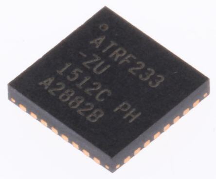
AT86RF233-ZU产品简介:
ICGOO电子元器件商城为您提供AT86RF233-ZU由Atmel设计生产,在icgoo商城现货销售,并且可以通过原厂、代理商等渠道进行代购。 AT86RF233-ZU价格参考¥37.00-¥46.25。AtmelAT86RF233-ZU封装/规格:RF 收发器 IC, IC 射频 TxRx + MCU 802.15.4,通用 ISM > 1GHz 6LoWPAN,Zigbee® 2.4GHz 32-VFQFN 裸露焊盘。您可以下载AT86RF233-ZU参考资料、Datasheet数据手册功能说明书,资料中有AT86RF233-ZU 详细功能的应用电路图电压和使用方法及教程。
Microchip Technology的AT86RF233-ZU是一款低功耗、高性能的无线射频(RF)收发器集成电路,主要应用于2.4 GHz ISM频段。该芯片支持多种无线通信协议,如Zigbee、6LoWPAN和Thread等,适用于物联网(IoT)、智能家居、工业自动化以及无线传感器网络等场景。

在智能家居领域,AT86RF233-ZU可用于智能照明控制、温控系统、安防设备和家用电器的无线互联。其低功耗特性使其非常适合电池供电设备,有助于延长设备续航时间。

在工业自动化中,该芯片可实现远程监控与数据采集,支持工厂设备的无线连接与管理,提高系统灵活性和可靠性。

此外,AT86RF233-ZU也广泛用于无线传感器网络,如环境监测、农业传感和健康监护等领域,便于实现多节点、远距离的数据传输与组网。

综上所述,AT86RF233-ZU凭借其低功耗、高集成度和良好的射频性能,成为众多无线通信应用的理想选择。
| 参数 | 数值 |
| 产品目录 | |
| 描述 | IC 2.4 GHZ ZIGBEE TRANSCEIVER射频收发器 2.4GHz ZigBee Transceiver |
| 产品分类 | RF 收发器集成电路 - IC |
| 品牌 | Atmel |
| 产品手册 | |
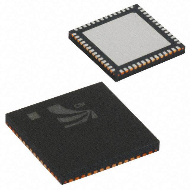
| 产品图片 |
|
| rohs | 符合RoHS无铅 / 符合限制有害物质指令(RoHS)规范要求 |
| 产品系列 | RF集成电路,射频收发器,Atmel AT86RF233-ZU- |
| 数据手册 | |
| 产品型号 | AT86RF233-ZU |
| PCN其它 | |
| 产品种类 | 射频收发器 |
| 其它名称 | AT86RF233ZU |
| 功率-输出 | 4dBm |
| 包装 | 托盘 |
| 商标 | Atmel |
| 天线连接器 | PCB,表面贴装 |
| 存储容量 | - |
| 安装风格 | SMD/SMT |
| 封装 | Tray |
| 封装/外壳 | 32-VFQFN 裸露焊盘 |
| 封装/箱体 | QFN-32 |
| 工作温度 | -40°C ~ 85°C |
| 工作电源电压 | 1.8 V to 3.6 V |
| 工厂包装数量 | 490 |
| 应用 | RF4CE |
| 接口类型 | SPI |
| 数据接口 | PCB,表面贴装 |
| 数据速率(最大值) | 2Mbps |
| 最大工作温度 | + 85 C |
| 最大数据速率 | 2000 kb/s |
| 标准包装 | 2,450 |
| 灵敏度 | -101dBm |
| 特色产品 | http://www.digikey.cn/product-highlights/cn/zh/atmel-at86rf233-transceiver/2359 |
| 电压-电源 | 1.8 V ~ 3.6 V |
| 电流-传输 | 13.8mA |
| 电流-接收 | 11.8mA |
| 调制或协议 | 802.15.4 Zigbee,6LoWPAN,ISM |
| 调制格式 | OQPSK |
| 输出功率 | 4 dBm |
| 频率 | 2.4GHz |
| 频率范围 | 2322 MHz to 2527 MHz |


- 商务部:美国ITC正式对集成电路等产品启动337调查
- 曝三星4nm工艺存在良率问题 高通将骁龙8 Gen1或转产台积电
- 太阳诱电将投资9.5亿元在常州建新厂生产MLCC 预计2023年完工
- 英特尔发布欧洲新工厂建设计划 深化IDM 2.0 战略
- 台积电先进制程称霸业界 有大客户加持明年业绩稳了
- 达到5530亿美元!SIA预计今年全球半导体销售额将创下新高
- 英特尔拟将自动驾驶子公司Mobileye上市 估值或超500亿美元
- 三星加码芯片和SET,合并消费电子和移动部门,撤换高东真等 CEO
- 三星电子宣布重大人事变动 还合并消费电子和移动部门
- 海关总署:前11个月进口集成电路产品价值2.52万亿元 增长14.8%

PDF Datasheet 数据手册内容提取
AT86RF233 Low Power, 2.4GHz Transceiver for ZigBee, RF4CE, IEEE 802.15.4, 6LoWPAN, and ISM Applications PRELIMINARY DATASHEET Features • High Performance RF-CMOS 2.4GHz radio transceiver targeted for IEEE® 802.15.4, ZigBee®, RF4CE, 6LoWPAN, and ISM applications • Industry leading link budget: • Receiver sensitivity -101dBm • Programmable TX output power from -17dBm up to +4dBm • Ultra-low current consumption: • DEEP_SLEEP = 0.02µA • TRX_OFF = 300µA • RX_ON = 11.8mA (LISTEN) • Smart Receiving Techniques enable further current reduction in LISTEN mode between 10 to 50% from 11.8mA • Desensitation will enable further reduction up to 1mA • BUSY_TX = 13.8mA (at max. transmit power) • Ultra-low supply voltage (1.8V to 3.6V) with internal regulator • Support for coin cell operation • Optimized for low BoM Cost and ease of production: • Few external components necessary (crystal, capacitors and antenna) • Easy to use interface: • Registers, frame buffer, and AES accessible through fast SPI • Only two microcontroller GPIO lines necessary • One interrupt pin from radio transceiver • Clock output with prescaler from radio transceiver • Radio transceiver features: • 128-byte FIFO (SRAM) for data buffering • Fully integrated, fast settling PLL to support Frequency Hopping • Supports 500kHz channel spacing • Battery monitor and Fast Wake-Up Time < 0.4msec • Special IEEE 802.15.4™ 2011 hardware support: • FCS computation and Clear Channel Assessment • RSSI measurement, Energy Detection and Link Quality Indication • MAC hardware accelerator: • Automated acknowledgement, CSMA-CA and retransmission • Automatic address filtering • Automated FCS check • Extended feature set hardware support: • AES 128-bit hardware accelerator • Antenna Diversity and RX/TX indication • Supported PSDU data rates: 250kb/s, 500kb/s, 1000kb/s and 2000kb/s • True Random Number Generation for security application • Reduced Power Consumption modes • Time and phase measurement support • Industrial and extended temperature range: • -40°C to +85°C and -40°C to +125°C • I/O and packages: • 32-pin Low-Profile QFN Package 5 x 5 x 0.9mm³ • RoHS/Fully Green • Compliant to EN 300 328/440, FCC-CFR-47 Part 15, ARIB STD-66, RSS-210 • Compliant to IEEE 802.15.4 2003/2006/2011 Atmel-8351E-MCU_Wireless-AT86RF233_Datasheet_072014
Table of Contents 1 Pin-out Diagram ............................................................................................................................ 7 1.1 Pin Descriptions ......................................................................................................................................................... 8 1.2 Analog and RF Pins ................................................................................................................................................... 9 1.2.1 Supply and Ground Pins ........................................................................................................................................................ 9 1.2.2 RF Pins .................................................................................................................................................................................. 9 1.2.3 Crystal Oscillator Pins .......................................................................................................................................................... 10 1.2.4 Analog Pin Summary ........................................................................................................................................................... 10 1.3 Digital Pins ............................................................................................................................................................... 11 1.3.1 Driver Strength Settings ....................................................................................................................................................... 11 1.3.2 Pull-up and Pull-down Configuration .................................................................................................................................... 11 2 Disclaimer .................................................................................................................................... 12 3 Overview ...................................................................................................................................... 12 4 General Circuit Description ........................................................................................................ 13 5 Application Schematic ................................................................................................................ 15 5.1 Basic Application Schematic .................................................................................................................................... 15 5.2 Extended Feature Set Application Schematic ......................................................................................................... 17 6 Microcontroller Interface ............................................................................................................ 19 6.1 Overview .................................................................................................................................................................. 19 6.2 SPI Timing Description ............................................................................................................................................ 20 6.3 SPI Protocol ............................................................................................................................................................. 21 6.3.1 Register Access Mode ......................................................................................................................................................... 21 6.3.2 Frame Buffer Access Mode ................................................................................................................................................. 22 6.3.3 SRAM Access Mode ............................................................................................................................................................ 24 6.4 Radio Transceiver Status information ..................................................................................................................... 25 6.4.1 Register Description ............................................................................................................................................................ 25 6.5 Radio Transceiver Identification .............................................................................................................................. 27 6.5.1 Register Description ............................................................................................................................................................ 27 6.6 Sleep/Wake-up and Transmit Signal (SLP_TR) ...................................................................................................... 29 6.7 Interrupt Logic .......................................................................................................................................................... 31 6.7.1 Overview .............................................................................................................................................................................. 31 6.7.2 Interrupt Mask Modes and Pin Polarity ................................................................................................................................ 32 6.7.3 Register Description ............................................................................................................................................................ 33 7 Operating Modes ......................................................................................................................... 36 7.1 Basic Operating Mode ............................................................................................................................................. 36 7.1.1 State Control ........................................................................................................................................................................ 37 7.1.2 Basic Operating Mode Description ...................................................................................................................................... 37 7.1.3 Interrupt Handling ................................................................................................................................................................ 41 7.1.4 Basic Operating Mode Timing ............................................................................................................................................. 42 7.1.5 Register Description ............................................................................................................................................................ 48 7.2 Extended Operating Mode ....................................................................................................................................... 50 7.2.1 State Control ........................................................................................................................................................................ 52 7.2.2 Configuration ....................................................................................................................................................................... 53 7.2.3 RX_AACK_ON – Receive with Automatic ACK ................................................................................................................... 54 7.2.4 TX_ARET_ON – Transmit with Automatic Frame Retransmission and CSMA-CA Retry .................................................... 63 7.2.5 Interrupt Handling ................................................................................................................................................................ 67 2 MCU Wireless AT86RF233 [PRELIMINARY DATASHEET] Atmel-8351E-MCU_Wireless-AT86RF233_Datasheet_072014
7.2.6 Register Summary ............................................................................................................................................................... 68 7.2.7 Register Description ............................................................................................................................................................ 68 8 Functional Description ............................................................................................................... 80 8.1 Introduction – IEEE 802.15.4-2006 Frame Format.................................................................................................. 80 8.1.1 PHY Protocol Data Unit (PPDU) .......................................................................................................................................... 80 8.1.2 MAC Protocol Data Unit (MPDU) ......................................................................................................................................... 82 8.2 Frame Filter .............................................................................................................................................................. 86 8.2.1 Configuration ....................................................................................................................................................................... 87 8.2.2 Handling of Reserved Frame Types .................................................................................................................................... 87 8.2.3 Register Description ............................................................................................................................................................ 88 8.2.4 Register Description – Address Registers ........................................................................................................................... 91 8.3 Frame Check Sequence (FCS) ............................................................................................................................... 96 8.3.1 Overview .............................................................................................................................................................................. 96 8.3.2 CRC Calculation .................................................................................................................................................................. 96 8.3.3 Automatic FCS Generation .................................................................................................................................................. 97 8.3.4 Automatic FCS Check ......................................................................................................................................................... 97 8.3.5 Register Description ............................................................................................................................................................ 97 8.4 Received Signal Strength Indicator (RSSI) ............................................................................................................. 99 8.4.1 Overview .............................................................................................................................................................................. 99 8.4.2 Reading RSSI ...................................................................................................................................................................... 99 8.4.3 Data Interpretation ............................................................................................................................................................... 99 8.4.4 Register Description .......................................................................................................................................................... 100 8.5 Energy Detection (ED) ........................................................................................................................................... 101 8.5.1 Overview ............................................................................................................................................................................ 101 8.5.2 Measurement Description .................................................................................................................................................. 101 8.5.3 Data Interpretation ............................................................................................................................................................. 102 8.5.4 Interrupt Handling .............................................................................................................................................................. 102 8.5.5 Register Description .......................................................................................................................................................... 103 8.6 Clear Channel Assessment (CCA) ........................................................................................................................ 104 8.6.1 Overview ............................................................................................................................................................................ 104 8.6.2 Configuration and Request ................................................................................................................................................ 104 8.6.3 Data Interpretation ............................................................................................................................................................. 105 8.6.4 Interrupt Handling .............................................................................................................................................................. 105 8.6.5 Measurement Time ............................................................................................................................................................ 105 8.6.6 Register Description .......................................................................................................................................................... 106 8.7 Link Quality Indication (LQI) .................................................................................................................................. 109 8.7.1 Overview ............................................................................................................................................................................ 109 8.7.2 Obtaining the LQI Value .................................................................................................................................................... 110 8.7.3 Data Interpretation ............................................................................................................................................................. 110 9 Module Description ................................................................................................................... 111 9.1 Receiver (RX) ........................................................................................................................................................ 111 9.1.1 Overview ............................................................................................................................................................................ 111 9.1.2 Frame Receive Procedure ................................................................................................................................................. 111 9.1.3 Configuration ..................................................................................................................................................................... 111 9.1.4 Register Description .......................................................................................................................................................... 112 9.2 Transmitter (TX) ..................................................................................................................................................... 115 9.2.1 Overview ............................................................................................................................................................................ 115 9.2.2 Frame Transmit Procedure ................................................................................................................................................ 115 9.2.3 Configuration ..................................................................................................................................................................... 115 9.2.4 TX Power Ramping ............................................................................................................................................................ 116 9.2.5 Register Description .......................................................................................................................................................... 116 3 MCU Wireless AT86RF233 [PRELIMINARY DATASHEET] Atmel-8351E-MCU_Wireless-AT86RF233_Datasheet_072014
9.3 Frame Buffer .......................................................................................................................................................... 118 9.3.1 Data Management ............................................................................................................................................................. 118 9.3.2 User accessible Frame Content......................................................................................................................................... 119 9.3.3 Interrupt Handling .............................................................................................................................................................. 119 9.4 Voltage Regulators (AVREG, DVREG) ................................................................................................................. 121 9.4.1 Overview ............................................................................................................................................................................ 121 9.4.2 Configuration ..................................................................................................................................................................... 122 9.4.3 Data Interpretation ............................................................................................................................................................. 122 9.4.4 Register Description .......................................................................................................................................................... 122 9.5 Battery Monitor (BATMON) .................................................................................................................................... 124 9.5.1 Overview ............................................................................................................................................................................ 124 9.5.2 Configuration ..................................................................................................................................................................... 124 9.5.3 Data Interpretation ............................................................................................................................................................. 124 9.5.4 Interrupt Handling .............................................................................................................................................................. 125 9.5.5 Register Description .......................................................................................................................................................... 125 9.6 Crystal Oscillator (XOSC) ...................................................................................................................................... 127 9.6.1 Overview ............................................................................................................................................................................ 127 9.6.2 Integrated Oscillator Setup ................................................................................................................................................ 127 9.6.3 External Reference Frequency Setup ................................................................................................................................ 128 9.6.4 Master Clock Signal Output (CLKM) .................................................................................................................................. 128 9.6.5 Register Description .......................................................................................................................................................... 129 9.7 Frequency Synthesizer (PLL) ................................................................................................................................ 132 9.7.1 Overview ............................................................................................................................................................................ 132 9.7.2 RF Channel Selection ........................................................................................................................................................ 132 9.7.3 PLL Settling Time and Frequency Agility ........................................................................................................................... 133 9.7.4 Calibration Loops ............................................................................................................................................................... 133 9.7.5 Interrupt Handling .............................................................................................................................................................. 134 9.7.6 Register Description .......................................................................................................................................................... 134 9.8 Automatic Filter Tuning (FTN) ............................................................................................................................... 139 9.8.1 Overview ............................................................................................................................................................................ 139 9.8.2 Register Description .......................................................................................................................................................... 139 10 Radio Transceiver Usage ....................................................................................................... 141 10.1 Frame Receive Procedure ................................................................................................................................... 141 10.2 Frame Transmit Procedure .................................................................................................................................. 142 11 AT86RF233 Extended Feature Set ......................................................................................... 143 11.1 Security Module (AES) ........................................................................................................................................ 143 11.1.1 Overview .......................................................................................................................................................................... 143 11.1.2 Security Module Preparation ........................................................................................................................................... 143 11.1.3 Security Key Setup .......................................................................................................................................................... 144 11.1.4 Security Operation Modes ............................................................................................................................................... 144 11.1.5 Data Transfer – Fast SRAM Access ................................................................................................................................ 147 11.1.6 Start of Security Operation and Status ............................................................................................................................ 147 11.1.7 SRAM Register Summary ................................................................................................................................................ 148 11.1.8 Register Description ........................................................................................................................................................ 148 11.2 Random Number Generator ................................................................................................................................ 151 11.2.1 Overview .......................................................................................................................................................................... 151 11.2.2 Register Description ........................................................................................................................................................ 151 11.3 High Data Rate Modes ........................................................................................................................................ 152 11.3.1 Overview .......................................................................................................................................................................... 152 11.3.2 High Data Rate Packet Structure ..................................................................................................................................... 153 11.3.3 High Data Rate Frame Buffer Access .............................................................................................................................. 154 4 MCU Wireless AT86RF233 [PRELIMINARY DATASHEET] Atmel-8351E-MCU_Wireless-AT86RF233_Datasheet_072014
11.3.4 High Data Rate Energy Detection .................................................................................................................................... 154 11.3.5 High Data Rate Mode Options ......................................................................................................................................... 154 11.3.6 Register Description ........................................................................................................................................................ 156 11.4 Antenna Diversity ................................................................................................................................................. 159 11.4.1 Overview .......................................................................................................................................................................... 159 11.4.2 Antenna Diversity Application Example ........................................................................................................................... 159 11.4.3 Antenna Diversity Sensitivity Control ............................................................................................................................... 160 11.4.4 Register Description ........................................................................................................................................................ 161 11.5 RX/TX Indicator ................................................................................................................................................... 164 11.5.1 Overview .......................................................................................................................................................................... 164 11.5.2 External RF-Front End Control ........................................................................................................................................ 164 11.5.3 Register Description ........................................................................................................................................................ 165 11.6 RX and TX Frame Time Stamping (TX_ARET) ................................................................................................... 166 11.6.1 Overview .......................................................................................................................................................................... 166 11.6.2 Register Description ........................................................................................................................................................ 166 11.7 Frame Buffer Empty Indicator .............................................................................................................................. 168 11.7.1 Overview .......................................................................................................................................................................... 168 11.7.2 Register Description ........................................................................................................................................................ 169 11.8 Dynamic Frame Buffer Protection........................................................................................................................ 170 11.8.1 Overview .......................................................................................................................................................................... 170 11.8.2 Register Description ........................................................................................................................................................ 170 11.9 Alternate Start-Of-Frame Delimiter ...................................................................................................................... 171 11.9.1 Overview .......................................................................................................................................................................... 171 11.9.2 Register Description ........................................................................................................................................................ 171 11.10 Reduced Power Consumption Mode (RPC) ...................................................................................................... 172 11.10.1 Overview ........................................................................................................................................................................ 172 11.10.2 RPC Methods and Elements.......................................................................................................................................... 172 11.10.3 Register Summary ......................................................................................................................................................... 175 11.11 Time-Of-Flight Module (TOM) ............................................................................................................................ 177 11.11.1 Overview ........................................................................................................................................................................ 177 11.11.2 Interrupt Handling .......................................................................................................................................................... 177 11.11.3 TOM Measurements ...................................................................................................................................................... 177 11.11.4 Register Summary ......................................................................................................................................................... 179 11.11.5 Frame Buffer Content Summary .................................................................................................................................... 180 11.12 Phase Difference Measurement ........................................................................................................................ 187 11.12.1 Overview ........................................................................................................................................................................ 187 11.12.2 Register Summary ......................................................................................................................................................... 187 12 Electrical Characteristics ....................................................................................................... 189 12.1 Absolute Maximum Ratings ................................................................................................................................. 189 12.2 Recommended Operating Range ........................................................................................................................ 189 12.3 Digital Pin Characteristics .................................................................................................................................... 190 12.4 Digital Interface Timing Characteristics ............................................................................................................... 190 12.5 General RF Specifications ................................................................................................................................... 191 12.6 Transmitter Characteristics .................................................................................................................................. 192 12.7 Receiver Characteristics ...................................................................................................................................... 192 12.8 Current Consumption Specifications ................................................................................................................... 193 12.9 Crystal Parameter Requirements ........................................................................................................................ 194 5 MCU Wireless AT86RF233 [PRELIMINARY DATASHEET] Atmel-8351E-MCU_Wireless-AT86RF233_Datasheet_072014
13 Typical Characteristics ........................................................................................................... 195 13.1 Active Supply Current .......................................................................................................................................... 195 13.1.1 P_ON and TRX_OFF states ............................................................................................................................................ 195 13.1.2 PLL_ON state .................................................................................................................................................................. 196 13.1.3 RX_ON state.................................................................................................................................................................... 197 13.1.4 TX_BUSY state................................................................................................................................................................ 198 13.1.5 SLEEP ............................................................................................................................................................................. 200 13.1.6 DEEP_SLEEP ................................................................................................................................................................. 200 13.2 State Transition Timing ........................................................................................................................................ 201 14 Register Reference ................................................................................................................. 203 15 Abbreviations .......................................................................................................................... 206 16 Ordering Information .............................................................................................................. 208 17 Soldering Information ............................................................................................................. 208 18 Package Thermal Properties .................................................................................................. 208 19 Package Drawing – 32QN2 ..................................................................................................... 209 Appendix A Continuous Transmission Test Mode ................................................................ 210 A.1 Overview ........................................................................................................................................................... 210 A.2 Configuration ..................................................................................................................................................... 210 A.3 Register Description .......................................................................................................................................... 212 Appendix B AT86RF233-ZF / AT86RF233-ZFR Extended Temperature Range .................... 213 B.1 Introduction ....................................................................................................................................................... 213 B.2 Reduced Feature Set ........................................................................................................................................ 213 B.3 Electrical Characteristics ................................................................................................................................... 213 B.3.1 Recommended Operating Range ............................................................................................................................... 213 B.3.2 General RF Specifications .......................................................................................................................................... 214 B.4 Typical Characteristics ...................................................................................................................................... 214 B.4.1 Active Supply Current ................................................................................................................................................. 214 B.4.2 State Transition Timing ............................................................................................................................................... 218 B.4.3 Receiver Performance ................................................................................................................................................ 219 B.4.4 Transmitter Performance ............................................................................................................................................ 220 Appendix C Errata ..................................................................................................................... 222 AT86RF233 Rev. A ...................................................................................................................................................... 222 References .................................................................................................................................... 223 Data Sheet Revision History ....................................................................................................... 224 Rev. 8315E–MCU Wireless–07/14 .............................................................................................................................. 224 Rev. 8351D–MCU Wireless–08/13 .............................................................................................................................. 224 Rev. 8351C–MCU Wireless–02/13 .............................................................................................................................. 224 Rev. 8351B–MCU Wireless–06/12 .............................................................................................................................. 224 Rev. 8351A–MCU Wireless–02/12 .............................................................................................................................. 224 6 MCU Wireless AT86RF233 [PRELIMINARY DATASHEET] Atmel-8351E-MCU_Wireless-AT86RF233_Datasheet_072014
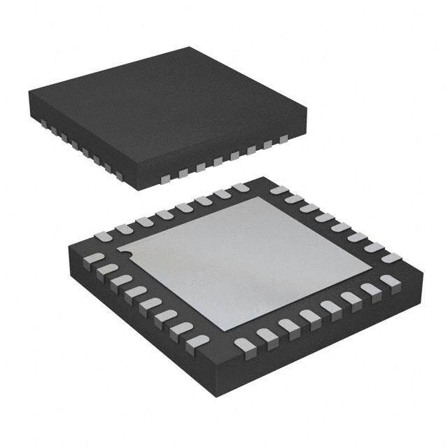
1 Pin-out Diagram Figure 1-1. Atmel AT86RF233 Pin-out Diagram. S S S D D S L1 L2 S S S D D S A A V V V V V V T T A A A A E A X X 32 31 30 29 28 27 26 25 DIG3 1 24 IRQ exposed paddle DIG4 2 AVSS 23 /SEL AVSS 3 22 MOSI RFP 4 21 DVSS AT86RF233 RFN 5 20 MISO AVSS 6 19 SCLK DVSS 7 18 DVSS /RST 8 17 CLKM 9 10 11 12 13 14 15 16 1 2 R S D D D S G G T S D D D S DI DI P_ DV DV DV EV DV L D S Note: 1. The exposed paddle is electrically connected to the die inside the package. It shall be soldered to the board to ensure electrical and thermal contact and good mechanical stability. 7 MCU Wireless AT86RF233 [PRELIMINARY DATASHEET] Atmel-8351E-MCU_Wireless-AT86RF233_Datasheet_072014
1.1 Pin Descriptions Table 1-1. Atmel AT86RF233 Pin Description. Pins Name Type Description 1 DIG3 Digital output (Ground) 1. RX/TX Indicator, see Section 11.5 2. If disabled, pull-down enabled (AVSS) 2 DIG4 Digital output (Ground) 1. RX/TX Indicator (DIG3 inverted), see Section 11.5 2. If disabled, pull-down enabled (AVSS) 3 AVSS Ground Ground for RF signals 4 RFP RF I/O Differential RF signal 5 RFN RF I/O Differential RF signal 6 AVSS Ground Ground for RF signals 7 DVSS Ground Digital ground 8 /RST Digital input Chip reset; active low 9 DIG1 Digital output (Ground) 1. Antenna Diversity RF switch control, see Section 11.4 2. If disabled, pull-down enabled (DVSS) 10 DIG2 Digital output (Ground) 1. Antenna Diversity RF switch control (DIG1 inverted), see Section 11.4 2. RX Frame Time Stamping, see Section 11.6 3. TX Frame Time Stamping, see Section 11.6 4. If functions disabled, pull-down enabled (DVSS) 11 SLP_TR Digital input Controls sleep, deep sleep, transmit start, receive states; active high, see Section 6.6 12 DVSS Ground Digital ground 13, 14 DVDD Supply Regulated 1.8V voltage regulator output or regulated voltage input; digital domain, see Section 9.4 15 DEVDD Supply External supply voltage; digital domain 16 DVSS Ground Digital ground 17 CLKM Digital output Master clock signal output; low if disabled, see Section 9.6 18 DVSS Ground Digital ground 19 SCLK Digital input SPI clock 20 MISO Digital output SPI data output (master input slave output) 21 DVSS Ground Digital ground 22 MOSI Digital input SPI data input (master output slave input) 23 /SEL Digital input SPI select, active low 24 IRQ Digital output 1. Interrupt request signal; active high or active low; configurable, see Section 6.7 2. Frame Buffer Empty Indicator; active high, see Section 11.7 25 XTAL2 Analog input Crystal pin, see Section 9.6 26 XTAL1 Analog input Crystal pin or external clock supply, see Section 9.6 27 AVSS Ground Analog ground 28 EVDD Supply External supply voltage, analog domain 29 AVDD Supply Regulated 1.8V voltage regulator; analog domain, see Section 9.4 30, 31, 32 AVSS Ground Analog ground Paddle AVSS Ground Analog ground; Exposed paddle of QFN package 8 MCU Wireless AT86RF233 [PRELIMINARY DATASHEET] Atmel-8351E-MCU_Wireless-AT86RF233_Datasheet_072014
1.2 Analog and RF Pins 1.2.1 Supply and Ground Pins EVDD, DEVDD EVDD and DEVDD are analog and digital supply voltage pins of the Atmel® AT86RF233 radio transceiver. AVDD, DVDD AVDD and DVDD are outputs of the internal voltage regulators and require bypass capacitors for stable operation. The voltage regulators are controlled independently by the radio transceivers state machine and are activated depending on the current radio transceiver state. The voltage regulators can be configured for external supply; for details, refer to Section 9.4. AVSS, DVSS AVSS and DVSS are analog and digital ground pins respectively. The analog and digital power domains should be separated on the PCB. 1.2.2 RF Pins RFN, RFP A differential RF port (RFP/RFN) provides common-mode rejection to suppress the switching noise of the internal digital signal processing blocks. At board-level, the differential RF layout ensures high receiver sensitivity by reducing spurious emissions originated from other digital ICs such as a microcontroller. The RF port is designed for a 100Ω differential load. A DC path between the RF pins is allowed; a DC path to ground or supply voltage is not allowed. A simplified schematic of the RF front end is shown in Figure 1-2. Figure 1-2. Simplified RF Front-end Schematic. PCB AT86RF233 LNA RX PA TX 0.9V CM Feedback M0 RXTX 9 MCU Wireless AT86RF233 [PRELIMINARY DATASHEET] Atmel-8351E-MCU_Wireless-AT86RF233_Datasheet_072014
The RF port DC values depend on the operating state; refer to Chapter 7. In TRX_OFF state, when the analog front-end is disabled (see Section 7.1.2.5), the RF pins are pulled to ground, preventing a floating voltage larger than 1.8V which is not allowed for the internal circuitry. In transmit mode, a control loop provides a common-mode voltage of 0.9V. Transistor M0 is off, allowing the PA to set the common-mode voltage. The common-mode capacitance at each pin to ground shall be < 30pF to ensure the stability of this common-mode feedback loop. In receive mode, the RF port provides a low-impedance path to ground when transistor M0, (see Figure 1-2) pulls the inductor center tap to ground. A DC voltage drop of 20mV across the on-chip inductor can be measured at the RF pins. 1.2.3 Crystal Oscillator Pins XTAL1, XTAL2 The pin 26 (XTAL1) of Atmel AT86RF233 is the input of the reference oscillator amplifier (XOSC), the pin 25 (XTAL2) is the output. A detailed description of the crystal oscillator setup and the related XTAL1/XTAL2 pin configuration can be found in Section 9.6. When using an external clock reference signal, XTAL1 shall be used as input pin. For further details, refer to Section 9.6.3. 1.2.4 Analog Pin Summary Table 1-2. Analog Pin Behavior – DC values. Pin Values and Conditions Comments RFP/RFN VDC = 0.9V (BUSY_TX) DC level at pins RFP/RFN for various transceiver states. VDC = 20mV (receive states) AC coupling is required if a circuitry with a DC path to ground or VDC = 0mV (otherwise) supply is used. Serial capacitance and capacitance of each pin to ground must be < 30pF. XTAL1/XTAL2 VDC = 0.9V at both pins DC level at pins XTAL1/XTAL2 for various transceiver states. CPAR = 3pF Parasitic capacitance (CPAR) of the pins must be considered as additional load capacitance to the crystal. DVDD VDC = 1.8V (all states, except SLEEP DC level at pin DVDD for various transceiver states. and DEEP_SLEEP) Supply pins (voltage regulator output) for the digital 1.8V VDC = 0mV (otherwise) voltage domain. The outputs shall be bypassed by 100nF. AVDD VDC = 1.8V (all states, except P_ON, DC level at pin AVDD for various transceiver states. SLEEP, DEEP_SLEEP, RESET, and Supply pin (voltage regulator output) for the analog 1.8V TRX_OFF) voltage domain. The outputs shall be bypassed by 100nF. VDC = 0mV (otherwise) 10 MCU Wireless AT86RF233 [PRELIMINARY DATASHEET] Atmel-8351E-MCU_Wireless-AT86RF233_Datasheet_072014
1.3 Digital Pins The Atmel AT86RF233 provides a digital microcontroller interface. The interface comprises a slave SPI (/SEL, SCLK, MOSI, and MISO) and additional control signals (CLKM, IRQ, SLP_TR, /RST, and DIG2). The microcontroller interface is described in detail in Chapter 6. Additional digital output signals DIG1, …, DIG4 are provided to control external blocks, that is for Antenna Diversity RF switch control or as an RX/TX Indicator, see Section 11.4 and Section 11.5 respectively. 1.3.1 Driver Strength Settings The driver strength of all digital output pins (MISO, IRQ, DIG1, …, DIG4) and CLKM pin are fixed. The capacitive load should be as small as possible as, not larger than 50pF. 1.3.2 Pull-up and Pull-down Configuration Pulling transistors are internally connected to all digital input pins in radio transceiver states P_ON (including reset during P_ON) and DEEP_SLEEP, refer to Section 7.1.2.1 and Section 7.1.2.4. Table 1-3 summarizes the pull-up and pull-down configuration. Table 1-3. Pull-Up / Pull-Down Configuration of Digital Input Pins. Pin H =ˆ pull-up, L =ˆ pull-down /RST H /SEL H SCLK L MOSI L SLP_TR(1) L Note: 1. Except SLP_TR pin for DEEP_SLEEP state. In all other radio transceiver states, including RESET, no pull-up or pull-down transistors are connected to any of the digital input pins mentioned in Table 1-3. Note: 2. In all other states, external circuitry should guaranty defined levels at all input pins. Floating input pins may cause unexpected functionality and increased power consumption, for example in SLEEP state. If the additional digital output signals DIG1, …, DIG4 are not activated, these pins are pulled-down to digital ground (DIG1/DIG2) or analog ground (DIG3/DIG4). 11 MCU Wireless AT86RF233 [PRELIMINARY DATASHEET] Atmel-8351E-MCU_Wireless-AT86RF233_Datasheet_072014
2 Disclaimer Typical values contained in this datasheet are based on simulations and testing. Minimum and maximum values are available when the radio transceiver has been fully characterized. 3 Overview The Atmel AT86RF233 is a feature rich, extremely low-power 2.4GHz radio transceiver designed for industrial and consumer ZigBee/IEEE 802.15.4, RF4CE, 6LoWPAN, and high data rate 2.4GHz ISM band applications. The AT86RF233 is a true SPI-to-antenna solution. All RF-critical components except the antenna, crystal, and de-coupling capacitors are integrated on-chip. MAC and AES hardware accelerators improve overall system power efficiency and timing. Therefore, the AT86RF233 is particularly suitable for applications like: • 2.4GHz IEEE 802.15.4 and ZigBee systems • RF4CE systems • Energy Harvesting systems • 6LoWPAN systems • Wireless sensor networks • Industrial Control • Residential and commercial automation • Health care • Consumer electronics • PC peripherals The AT86RF233 can be operated by using an external microcontroller like Atmel AVR® microcontrollers. A comprehensive software programming description can be found in reference [7]. 12 MCU Wireless AT86RF233 [PRELIMINARY DATASHEET] Atmel-8351E-MCU_Wireless-AT86RF233_Datasheet_072014
4 General Circuit Description The Atmel AT86RF233 single-chip radio transceiver provides a complete radio transceiver interface between an antenna and a microcontroller. It comprises the analog radio, digital modulation and demodulation including time and frequency synchronization, as well as data buffering. A single 128-byte TRX buffer stores receive or transmit data. Communication between transmitter and receiver is based on direct sequence spread spectrum with different modulation schemes and spreading codes. The AT86RF233 block diagram is shown in Figure 4-1. Figure 4-1. AT86RF233 Block Diagram. 1 2 L L A A T T X X ext. PA and Power XOSC AVREG Configuration Registers DIG3/4 Control PA PLL TX Data /SEL TX BBP DVREG SPI MISO (Slave) MOSI RFP Frame SCLK FTN, BATMON Buffer RFN IRQ LNA PPF BPF Limiter ADC RX BBP AES CLKM DIG2 /RST RSSI AGC SLP_TR Control Logic AD Antenna Diversity DIG1/2 Analog Domain Digital Domain The number of external components is minimized such that only the antenna, the crystal and decoupling capacitors are required. The bidirectional differential antenna pins (RFP, RFN) are used for transmission and reception, thus no external antenna switch is needed. Control of an external power amplifier is supported by two digital control signals (differential operation). The received RF signal at pin 5 (RFN) and pin 6 (RFP) is differentially fed through the low-noise amplifier (LNA) to the RF filter (PPF) to generate a complex signal, driving the integrated channel filter (BPF). The limiting amplifier provides sufficient gain to drive the succeeding analog-to-digital converter (ADC) and generates a digital RSSI signal. The ADC output signal is sampled by the digital base band receiver (RX BBP). The transmit modulation scheme is offset-QPSK (O-QPSK) with half-sine pulse shaping and 32-length block coding (spreading) according to [1], [2] and [3]. The modulation signal is generated in the digital transmitter (TX BBP) and applied to the fractional-N frequency synthesis (PLL), to ensure the coherent phase modulation required for 13 MCU Wireless AT86RF233 [PRELIMINARY DATASHEET] Atmel-8351E-MCU_Wireless-AT86RF233_Datasheet_072014
demodulation of O-QPSK signals. The frequency-modulated signal is fed to the power amplifier (PA). Two on-chip low-dropout voltage regulators (A|DVREG) provide regulated analog and digital 1.8V supply outputs. An internal 128-byte RAM for RX and TX (Frame Buffer) buffers the data to be transmitted or the received data. The configuration of the Atmel AT86RF233, reading and writing of Frame Buffer is controlled by the SPI interface and additional control lines. The AT86RF233 further contains comprehensive hardware-MAC support (Extended Operating Mode) and a security engine (AES) to improve the overall system power efficiency and timing. The stand-alone 128-bit AES engine can be accessed in parallel to all PHY operational transactions and states using the SPI interface, except during SLEEP and DEEP_SLEEP states. For applications not necessarily targeting IEEE 802.15.4 compliant networks, the radio transceiver also supports alternative data rates up to 2000kb/s. For long-range applications or to improve the reliability of a RF connection the RF performance can further be improved by using an external RF front-end or Antenna Diversity. Both operation modes are supported by the AT86RF233 with dedicated control pins DIG1, …, DIG4 without the interaction of the microcontroller. Additional features of the Extended Feature Set, see Chapter 11, are provided to simplify the interaction between radio transceiver and microcontroller. 14 MCU Wireless AT86RF233 [PRELIMINARY DATASHEET] Atmel-8351E-MCU_Wireless-AT86RF233_Datasheet_072014
5 Application Schematic 5.1 Basic Application Schematic A basic application schematic of the Atmel AT86RF233 with a single-ended RF connector is shown in Figure 5-1. The 50Ω single-ended RF input is transformed to the 100Ω differential RF port impedance using balun B1. The capacitors C1 and C2 provide AC coupling of the RF input to the RF port, optional capacitor C4 improves matching if required. Figure 5-1. Basic Application Schematic. CB2 CX1 CX2 XTAL VDD CB1 32 31 30 29 28 27 26 25 S S S D D S 1 2 1 DIG3 AVS AVS AVS AVD EVD AVS XTAL XTAL IRQ 24 ce a 2 DIG4 /SEL 23 erf nt C1 3 AVSS MOSI 22 gital I RF 4 RFP DVSS 21 Di B1 AT86RF233 C4 5 RFN MISO 20 C2 6 AVSS SCLK 19 7 DVSS DVSS 18 R1 8 /RSTDIG1 DIG2 SLP_TR DVSS DVDD DVDD DEVDD DVSSCLKM 17 C3 9 10 11 12 13 14 15 16 VDD CB3 CB4 The power supply decoupling capacitors (CB2, CB4) are connected to the external analog supply pin 28 (EVDD) and external digital supply pin 15 (DEVDD). Capacitors CB1 and CB3 are bypass capacitors for the integrated analog and digital voltage regulators to ensure stable operation. All bypass capacitors should be placed as close as possible to the pins and should have a low-resistance and low-inductance connection to ground to achieve the best performance. The crystal (XTAL), the two load capacitors (CX1, CX2), and the internal circuitry connected to pins XTAL1 and XTAL2 form the crystal oscillator. To achieve the best accuracy and stability of the reference frequency, large parasitic capacitances should be avoided. Crystal lines should be routed as short as possible and not in proximity of digital I/O signals. This is especially required for the High Data Rate Modes; refer to Section 11.3. Crosstalk from digital signals on the crystal pins or the RF pins can degrade the system performance. Therefore, a low-pass filter (C3, R1) is placed close to the Atmel AT86RF233 CLKM output pin to reduce the emission of CLKM signal harmonics. 15 MCU Wireless AT86RF233 [PRELIMINARY DATASHEET] Atmel-8351E-MCU_Wireless-AT86RF233_Datasheet_072014
This is not needed if pin 17 (CLKM) is not used as a microcontroller clock source. In this case, pin 17 (CLKM) output should be disabled during device initialization. The ground plane of the application board should be separated into four independent fragments: the analog, the digital, the antenna, and the XTAL ground plane. The exposed paddle shall act as the reference point of the individual grounds. Note: 1. The pins DIG1, DIG2, DIG3, and DIG4 are connected to ground in the Basic Application Schematic; refer to Figure 5-1. Special programming of these pins requires a different schematic; refer to Section 5.2. Table 5-1. Exemplary Bill of Materials (BoM) for Basic Application Schematic. Symbol Description Value Manufacturer Part Number Comment B1 SMD balun 2.45GHz Wuerth 748421245 2.45GHz Balun B1 SMD balun / filter 2.45GHz Johanson 2450BM15A0015 2.45GHz Balun / Filter (alternatively) Technology CB1 LDO VREG 100nF Generic X7R 10% 16V CB3 bypass capacitor (0402) CB2 Power supply decoupling 1µF AVX 0603YD105KAT2A X5R 10% 16V CB4 Murata GRM188R61C105KA12D (0603) CX1, CX2 Crystal load capacitor 12pF AVX 06035A120JA COG 5% 50V Murata GRM1555C1H120JA01D (0402) C1, C2 RF coupling capacitor 22pF Murata GRM1555C1H220JA01J C0G 5% 50V Epcos B37920 (0402 or 0603) AVX 06035A220JAT2A C3 CLKM low-pass 2.2pF AVX 06035A229DA COG ±0.5pF 50V filter capacitor Murata GRP1886C1H2R0DA01 (0603) Designed for fCLKM = 1MHz C4 (optional) RF matching Value depends on final PCB implementation R1 CLKM low-pass 680Ω Designed for fCLKM = 1MHz filter resistor XTAL Crystal CX-4025 16MHz ACAL Taitjen XWBBPL-F-1 SX-4025 16MHz Siward A207-011 16 MCU Wireless AT86RF233 [PRELIMINARY DATASHEET] Atmel-8351E-MCU_Wireless-AT86RF233_Datasheet_072014
5.2 Extended Feature Set Application Schematic The Atmel AT86RF233 supports additional features like: • Security Module (AES) Section 11.1 • Random Number Generator Section 11.2 • High Data Rate Modes Section 11.3 • Antenna Diversity uses pins DIG1(/2) Section 11.4 • RX/TX Indicator uses pins DIG3/4 Section 11.5 • RX and TX Frame Time Stamping (TX_ARET) uses pin DIG2 Section 11.6 • Frame Buffer Empty Indicator uses pin IRQ Section 11.7 • Dynamic Frame Buffer Protection Section 11.8 • Alternate Start-Of-Frame Delimiter Section 11.9 • Reduced Power Consumption Mode (RPC) Section 11.10 • TOM Measurements Section 11.11 • Phase Difference Measurement Section 11.12 An extended feature set application schematic illustrating the use of the AT86RF233 Extended Feature Set, see Chapter 11, is shown in Figure 5-2. Although this example shows all additional hardware features combined, it is possible to use all features separately or in various combinations. Figure 5-2. Extended Feature Application Schematic. CB2 CX1 CX2 XTAL VDD CB1 32 31 30 29 28 27 26 25 S S S D D S 1 2 ANT0 1 DIG3 AVS AVS AVS AVD EVD AVS XTAL XTAL IRQ 24 ce a 2 DIG4 /SEL 23 erf nt N2 3 AVSS MOSI 22 al I git h LNA h n 4 RFP DVSS 21 Di SW2 RF-Switc PA RF-Switc Balu 5 RFN AT86RF233 MISO 20 6 AVSS SCLK 19 N1 SW1 B1 7 DVSS DVSS 18 R1 ANT1 8 /RSTDIG1 DIG2 SLP_TR DVSS DVDD DVDD DEVDD DVSSCLKM 17 C3 9 10 11 12 13 14 15 16 VDD CB3 CB4 17 MCU Wireless AT86RF233 [PRELIMINARY DATASHEET] Atmel-8351E-MCU_Wireless-AT86RF233_Datasheet_072014
In this example, a balun (B1) transforms the differential RF signal at the Atmel AT86RF233 radio transceiver RF pins (RFP/RFN) to a single ended RF signal, similar to the Basic Application Schematic; refer to Figure 5-1. During receive mode the radio transceiver searches for the most reliable RF signal path using the Antenna Diversity algorithm. One antenna is selected (SW2) by the Antenna Diversity RF switch control pin 9 (DIG1), refer to Section 11.4. The RX signal is amplified by an optional low-noise amplifier (N2) and fed to the radio transceiver using the RX/TX switch (SW1). During transmit mode the AT86RF233 TX signal is amplified using an external PA (N1) and fed to the antennas via an RF switch (SW2). These switches are controlled by the RX/TX Indicator, represented by the differential pin pair DIG3/DIG4, refer to Section 11.5. RX and TX Frame Time stamping is implemented through pin 10 (DIG2), refer to Section 11.6. The Security Module (AES), Random Number Generator, High Data Rate Modes, Frame Buffer Empty Indicator, Dynamic Frame Buffer Protection, Alternate Start-Of- Frame Delimiter or Reduced Power Consumption Mode (RPC) do not require specific circuitry to operate, for details refer to Section 11.1, Section 11.2, Section 11.3, Section 11.7, Section 11.8, Section 11.9 and Section 11.10. 18 MCU Wireless AT86RF233 [PRELIMINARY DATASHEET] Atmel-8351E-MCU_Wireless-AT86RF233_Datasheet_072014
6 Microcontroller Interface 6.1 Overview This section describes the Atmel AT86RF233 to microcontroller interface. The interface comprises a slave SPI and additional control signals; see Figure 6-1. The SPI timing and protocol are described below. Figure 6-1. Microcontroller to AT86RF233 Interface. Microcontroller SPI AT86RF233 er /SEL /SEL /SEL e Mast MOSI MOSI MOSI Slav SPI - SMCISLOK SMCISLOK MSCISLOK SPI - GPIO1/CLK CLKM CLKM GPIO2/IRQ IRQ IRQ GPIO3 SLP_TR SLP_TR GPIO4 /RST /RST GPIO5 DIG2 DIG2 Microcontrollers with a master SPI such as Atmel AVR family interface directly to the AT86RF233. The SPI is used for register, Frame Buffer, SRAM and AES access. The additional control signals are connected to the GPIO/IRQ interface of the microcontroller. Table 6-1 introduces the radio transceiver I/O signals and their functionality. Table 6-1. Signal Description of Microcontroller Interface. Signal Description /SEL SPI select signal, active low MOSI SPI data (master output slave input) signal MISO SPI data (master input slave output) signal SCLK SPI clock signal CLKM Optional, Clock output, refer to Section 9.6.4, usable as: - microcontroller clock source and/or MAC timer reference - high precision timing reference IRQ Interrupt request signal, further used as: - Frame Buffer Empty indicator, refer to Section 11.7 SLP_TR Multi purpose control signal (functionality is state dependent, see Section 6.6): - Sleep/Wakeup enable/disable SLEEP state - Sleep/Wakeup enable/disable DEEP_SLEEP state - TX start BUSY_TX_(ARET) state /RST AT86RF233 reset signal, active low DIG2 Optional, - IRQ_2 (RX_START) for RX Frame Time Stamping, see Section 11.6 - Signals frame transmit within TX_ARET mode for TX Time Stamping 19 MCU Wireless AT86RF233 [PRELIMINARY DATASHEET] Atmel-8351E-MCU_Wireless-AT86RF233_Datasheet_072014
6.2 SPI Timing Description Pin 17 (CLKM) can be used as a microcontroller master clock source. If the microcontroller derives the SPI master clock (SCLK) directly from CLKM, the SPI operates in synchronous mode, otherwise in asynchronous mode. In asynchronous mode, the maximum SCLK frequency f is limited to 7.5MHz. The async signal at pin 17 (CLKM) is not required to derive SCLK and may be disabled to reduced power consumption and spurious emissions. Figure 6-2 and Figure 6-3 illustrate the SPI timing and introduces its parameters. The corresponding timing parameter definitions t – t are defined in Section 12.4. 1 9 Figure 6-2. SPI Timing, Global Map and Definition of Timing Parameters t , t , t , t . 5 6 8 9 t9 t8 /SEL SCLK MOSI 7 6 5 4 3 2 1 0 7 6 5 4 3 2 1 0 t5 t6 MISO Bit 7 Bit 6 Bit 5 Bit 4 Bit 3 Bit 2 Bit 1 Bit 0 Bit 7 Bit 6 Bit 5 Bit 4 Bit 3 Bit 2 Bit 1 Bit 0 Figure 6-3. SPI Timing, Detailed Drawing of Timing Parameters t to t . 1 4 /SEL SCLK t3 t4 MOSI Bit 7 Bit 6 Bit 5 t1 t2 MISO Bit 7 Bit 6 Bit 5 The SPI is based on a byte-oriented protocol and is always a bidirectional communication between the master and slave. The SPI master starts the transfer by asserting /SEL = L. Then the master generates eight SPI clock cycles to transfer one byte to the radio transceiver (via MOSI). At the same time, the slave transmits one byte to the master (via MISO). When the master wants to receive one byte of data from the slave, it must also transmit one byte to the slave. All bytes are transferred with the MSB first. An SPI transaction is finished by releasing /SEL = H. An SPI register access consists of two bytes, a Frame Buffer or SRAM access of at least two or more bytes as described in Section 6.3. /SEL = L enables the MISO output driver of the Atmel AT86RF233. The MSB of MISO is valid after t (see Section 12.4) and is updated on each SCLK falling edge. If the 1 driver is disabled, there is no internal pull-up transistor connected to it. Driving the appropriate signal level must be ensured by the master device or an external pull-up resistor. Note: 1. When both /SEL and /RST are active, the MISO output driver is also enabled. 20 MCU Wireless AT86RF233 [PRELIMINARY DATASHEET] Atmel-8351E-MCU_Wireless-AT86RF233_Datasheet_072014
Referring to Figure 6-2 and Figure 6-3, Atmel AT86RF233 MOSI is sampled at the rising edge of the SCLK signal and the output is set at the falling edge of SCLK. The signal must be stable before and after the rising edge of SCLK as specified by t and t , 3 4 refer to Section 12.4 parameters. This SPI operational mode is commonly known as “SPI mode 0”. 6.3 SPI Protocol Each SPI sequence starts with transferring a command byte from the SPI master via MOSI (see Table 6-2) with the MSB first. This command byte defines the SPI access mode and additional mode-dependent information. Table 6-2. SPI Command Byte Definition. Bit 7 Bit 6 Bit 5 Bit 4 Bit 3 Bit 2 Bit 1 Bit 0 Access Mode Access Type 1 0 Register address [5:0] Register access Read access 1 1 Register address [5:0] Write access 0 0 1 Reserved Frame Buffer access Read access 0 1 1 Reserved Write access 0 0 0 Reserved SRAM access Read access 0 1 0 Reserved Write access Each SPI transfer returns bytes back to the SPI master on MISO output pin. The content of the first byte (see value “PHY_STATUS“ in Figure 6-4 to Figure 6-14) is set to zero after reset. To transfer status information of the radio transceiver to the microcontroller, the content of the first byte can be configured with register bits SPI_CMD_MODE (register 0x04, TRX_CTRL_1). For details, refer to Section 6.4.1. Note: 1. Return values on MISO stated as XX shall be ignored by the microcontroller. The different access modes are described within the following sections. 6.3.1 Register Access Mode Register Access Mode is used to read and write AT86RF233 regsisters (register address from 0x00 up to 0x3F). A register access mode is a two-byte read/write operation initiated by /SEL = L. The first transferred byte on MOSI is the command byte including an identifier bit (bit[7] = 1), a read/write select bit (bit[6]), and a 6-bit register address. On read access, the content of the selected register address is returned in the second byte on MISO (see Figure 6-4). Figure 6-4. Packet Structure - Register Read Access. byte 1 (command byte) byte 2 (data byte) MOSI 1 0 ADDRESS[5:0] XX MISO PHY_STATUS(1) READ DATA[7:0] Note: 1. Each SPI access can be configured to return radio controller status information (PHY_STATUS) on MISO, for details refer to Section 6.4. On write access, the second byte transferred on MOSI contains the write data to the selected address (see Figure 6-5). 21 MCU Wireless AT86RF233 [PRELIMINARY DATASHEET] Atmel-8351E-MCU_Wireless-AT86RF233_Datasheet_072014
Figure 6-5. Packet Structure - Register Write Access. byte 1 (command byte) byte 2 (data byte) MOSI 1 1 ADDRESS[5:0] WRITE DATA[7:0] MISO PHY_STATUS XX Each register access must be terminated by setting /SEL = H. Figure 6-6 illustrates a typical SPI sequence for a register access sequence for write and read respectively. Figure 6-6. Example SPI Sequence – Register Access Mode. Register Write Access Register Read Access /SEL SCLK MOSI WRITE COMMAND WRITE DATA READ COMMAND XX MISO PHY_STATUS XX PHY_STATUS READ DATA 6.3.2 Frame Buffer Access Mode Frame Buffer Access Mode is used to read and write Atmel AT86RF233 frame buffer. The frame buffer address is always reset to zero and incremented to access PSDU, LQI, ED and RX_STATUS data. The Frame Buffer can hold up to 128-byte of one PHY service data unit (PSDU) IEEE 802.15.4 data frame. A detailed description of the Frame Buffer can be found in Section 9.3. An introduction to the IEEE 802.15.4 frame format can be found in Section 8.1. Each access starts with /SEL = L followed by a command byte on MOSI. Each frame read or write access command byte is followed by the PHR data byte, indicating the frame length, followed by the PSDU data, see Figure 6-7 and Figure 6-8. In Frame Buffer Access Mode during buffer reads, the PHY header (PHR) and the PSDU data are transferred via MISO following PHY_STATUS byte. Once the PSDU data is uploaded, three more bytes are transferred containing the link quality indication (LQI) value, the energy detection (ED) value, and the status information (RX_STATUS) of the received frame, for LQI details refer to Section 8.7. The Figure 6-7 illustrates the packet structure of a Frame Buffer read access. Note: 1. The frame buffer read access can be terminated immediately at any time by setting pin 23 (/SEL) = H, for example after reading the PHR byte only. Figure 6-7. Packet Structure - Frame Read Access. byte 1 (command byte) byte 2 (data byte) byte 3 (data byte) byte n-1 (data byte) byte n (data byte) MOSI 0 0 1 reserved[4:0] XX XX XX XX MISO PHY_STATUS PHR[7:0] PSDU[7:0] ED[7:0] RX_STATUS[7:0] 22 MCU Wireless AT86RF233 [PRELIMINARY DATASHEET] Atmel-8351E-MCU_Wireless-AT86RF233_Datasheet_072014
The structure of RX_STATUS is described in Table 6-3. Table 6-3. Structure of RX_STATUS. Bit 7 6 5 4 RX_CRC_VALID TRAC_STATUS RX_STATUS Read/Write R R R R Reset value 0 0 0 0 Bit 3 2 1 0 reserved RX_STATUS Read/Write R R R R Reset value 0 0 0 0 Note: 2. More information to RX_CRC_VALID, see Section 8.3.5, and to TRAC_STATUS, see Section 7.2.6. On frame buffer write access the second byte transferred on MOSI contains the frame length (PHR field) followed by the payload data (PSDU) as shown by Figure 6-8. Figure 6-8. Packet Structure - Frame Write Access. byte 1 (command byte) byte 2 (data byte) byte 3 (data byte) byte n-1 (data byte) byte n (data byte) MOSI 0 1 1 reserved[4:0] PHR[7:0] PSDU[7:0] PSDU[7:0] PSDU[7:0] MISO PHY_STATUS XX XX XX XX The number of bytes n for one frame buffer access is calculated as follows: Read Access: n = 5 + frame_length [PHY_STATUS, PHR byte, PSDU data, LQI, ED, and RX_STATUS] Write Access: n = 2 + frame_length [command byte, PHR byte, and PSDU data] The maximum value of frame_length is 127 bytes. That means that n ≤ 132 for Frame Buffer read and n ≤ 129 for Frame Buffer write accesses. Each read or write of a data byte automatically increments the address counter of the Frame Buffer until the access is terminated by setting /SEL = H. A Frame Buffer read access can be terminated at any time without any consequences by setting /SEL = H, for example after reading the frame length byte only. A successive Frame Buffer read operation starts again with the PHR field. The content of the Atmel AT86RF233 Frame Buffer is overwritten by a new received frame or a Frame Buffer write access. Figure 6-9 and Figure 6-10 illustrate an example SPI sequence of a Frame Buffer access to read a frame with 2-byte PSDU and write a frame with 4-byte PSDU. Figure 6-9. Example SPI Sequence - Frame Buffer Read of a Frame with 2-byte PSDU. /SEL SCLK MOSI COMMAND XX XX XX XX XX XX MISO PHY_STATUS PHR PSDU 1 PSDU 2 LQI ED RX_STATUS 23 MCU Wireless AT86RF233 [PRELIMINARY DATASHEET] Atmel-8351E-MCU_Wireless-AT86RF233_Datasheet_072014
Figure 6-10. Example SPI Sequence - Frame Buffer Write of a Frame with 4-byte PSDU. /SEL SCLK MOSI COMMAND PHR PSDU 1 PSDU 2 PSDU 3 PSDU 4 MISO PHY_STATUS XX XX XX XX XX Access violations during a Frame Buffer read or write access are indicated by interrupt IRQ_6 (TRX_UR). For further details, refer to Section 9.3. Notes: 1. The Frame Buffer is shared between RX and TX operations, the frame data is overwritten by freshly received data frames. If an existing TX payload data frame is to be retransmitted, it must be ensured that no TX data is overwritten by newly received RX data. 2. To avoid overwriting during receive Dynamic Frame Buffer Protection can be enabled, refer to Section 11.8. 3. For exceptions, receiving acknowledgement frames in Extended Operating Mode (TX_ARET) refer to Section 7.2.4. 6.3.3 SRAM Access Mode The SRAM access mode is used to read and write Atmel AT86RF233 frame buffer beginning with a specified byte address. It enables to access dedicated buffer data directly from a desired address without a need of incrementing the frame buffer from the top. The SRAM access mode allows accessing dedicated bytes within the Frame Buffer or AES address space, refer to Section 11.1. This may reduce the SPI traffic. During frame receive, after occurrence of IRQ_2 (RX_START), an SRAM access can be used to upload the PHR field while preserving Dynamic Frame Buffer Protection, see Section 11.8. Each SRAM access starts with /SEL = L. The first transferred byte on MOSI shall be the command byte and must indicate an SRAM access mode according to the definition in Table 6-2. The following byte indicates the start address of the write or read access. SRAM address space: • Frame Buffer: 0x00 to 0x7F • AES: 0x82 to 0x94 On SRAM read access, one or more bytes of read data are transferred on MISO starting with the third byte of the access sequence; refer to Figure 6-11. Figure 6-11. Packet Structure – SRAM Read Access. byte 1 (command byte) byte 2 (address) byte 3 (data byte) byte n-1 (data byte) byte n (data byte) MOSI 0 0 0 reserved[4:0] ADDRESS[7:0] XX XX XX MISO PHY_STATUS XX DATA[7:0] DATA[7:0] DATA[7:0] On SRAM write access, one or more bytes of write data are transferred on MOSI starting with the third byte of the access sequence; refer to Figure 6-12. Do not attempt to read or write bytes beyond the SRAM buffer size. 24 MCU Wireless AT86RF233 [PRELIMINARY DATASHEET] Atmel-8351E-MCU_Wireless-AT86RF233_Datasheet_072014
Figure 6-12. Packet Structure – SRAM Write Access. byte 1 (command byte) byte 2 (address) byte 3 (data byte) byte n-1 (data byte) byte n (data byte) MOSI 0 1 0 reserved[4:0] ADDRESS[7:0] DATA[7:0] DATA[7:0] DATA[7:0] MISO PHY_STATUS XX XX XX XX As long as /SEL = L, every subsequent byte read or byte write increments the address counter of the Frame Buffer until the SRAM access is terminated by /SEL = H. Figure 6-13 and Figure 6-14 illustrate an example SPI sequence of an Atmel AT86RF233 SRAM access to read and write a data package of five byte length, respectively. Figure 6-13. Example SPI Sequence – SRAM Read Access of a 5-byte Data Package. /SEL SCLK MOSI COMMAND ADDRESS XX XX XX XX XX MISO PHY_STATUS XX DATA 1 DATA 2 DATA 3 DATA 4 DATA 5 Figure 6-14. Example SPI Sequence – SRAM Write Access of a 5-byte Data Package. /SEL SCLK MOSI COMMAND ADDRESS DATA 1 DATA 2 DATA 3 DATA 4 DATA 5 MISO PHY_STATUS XX XX XX XX XX XX Notes: 1. The SRAM access mode is not intended to be used as an alternative to the Frame Buffer access modes (see Section 6.3.2). 2. Frame Buffer access violations are not indicated by a TRX_UR interrupt when using the SRAM access mode, for further details refer to Section 9.3.3. 6.4 Radio Transceiver Status information Each Atmel AT86RF233 SPI access can return radio transceiver status information which is a first byte transmitted out of MISO output as the serial data is being shifted into MOSI input. Radio transceiver status information (PHY_STATUS) can be configured using register bits SPI_CMD_MODE (register 0x04, TRX_CTRL_1) to return TRX_STATUS, PHY_RSSI or IRQ_STATUS register as shown in below. 6.4.1 Register Description Note: 1. Throughout this datasheet, underlined values indicate reset settings. Register 0x04 (TRX_CTRL_1): The TRX_CTRL_1 register is a multi-purpose register to control various operating modes and settings of the radio transceiver. 25 MCU Wireless AT86RF233 [PRELIMINARY DATASHEET] Atmel-8351E-MCU_Wireless-AT86RF233_Datasheet_072014
Figure 6-15. Register TRX_CTRL_1. Bit 7 6 5 4 0x04 TX_AUTO_CRC_ PA_EXT_EN IRQ_2_EXT_EN RX_BL_CTRL TRX_CTRL_1 ON Read/Write R/W R/W R/W R/W Reset value 0 0 1 0 Bit 3 2 1 0 0x04 SPI_CMD_MODE IRQ_MASK_MODE IRQ_POLARITY TRX_CTRL_1 Read/Write R/W R/W R/W R/W Reset value 0 0 1 0 • Bit 3:2 - SPI_CMD_MODE Each SPI transfer returns bytes back to the SPI master. The content of the first byte (PHY_STATUS) can be configured using register bits SPI_CMD_MODE. Table 6-4. SPI_CMD_MODE. Register Bits Value Description SPI_CMD_MODE 0 Default (empty, all bits zero) 1 Monitor TRX_STATUS register 2 Monitor PHY_RSSI register 3 Monitor IRQ_STATUS register 26 MCU Wireless AT86RF233 [PRELIMINARY DATASHEET] Atmel-8351E-MCU_Wireless-AT86RF233_Datasheet_072014
6.5 Radio Transceiver Identification Atmel AT86RF233 can be identified by four registers. One 8-bit register contains a unique part number (PART_NUM) and one register contains the corresponding 8-bit version number (VERSION_NUM). Two additional 8-bit registers contain the JEDEC manufacture ID. 6.5.1 Register Description Register 0x1C (PART_NUM): The register PART_NUM can be used for the radio transceiver identification and includes the part number of the device. Figure 6-16. Register PART_NUM. Bit 7 6 5 4 0x1C PART_NUM PART_NUM Read/Write R R R R Reset value 0 0 0 0 Bit 3 2 1 0 0x1C PART_NUM PART_NUM Read/Write R R R R Reset value 1 0 1 1 • Bit 7:0 - PART_NUM Table 6-5. PART_NUM. Register Bits Value Description PART_NUM 0x0B AT86RF233 part number Register 0x1D (VERSION_NUM): The register VERSION_NUM can be used for the radio transceiver identification and includes the version number of the device. Figure 6-17. Register VERSION_NUM. Bit 7 6 5 4 0x1D VERSION_NUM VERSION_NUM Read/Write R R R R Reset value 0 0 0 0 Bit 3 2 1 0 0x1D VERSION_NUM VERSION_NUM Read/Write R R R R Reset value 0 0 0 1 • Bit 7:0 - VERSION_NUM Table 6-6. VERSION_NUM. Register Bits Value Description VERSION_NUM 0x01 Revision A 0x02 Revision B 27 MCU Wireless AT86RF233 [PRELIMINARY DATASHEET] Atmel-8351E-MCU_Wireless-AT86RF233_Datasheet_072014
Register 0x1E (MAN_ID_0): Part one of the JEDEC manufacturer ID. Figure 6-18. Register MAN_ID_0. Bit 7 6 5 4 0x1E MAN_ID_0 MAN_ID_0 Read/Write R R R R Reset value 0 0 0 1 Bit 3 2 1 0 0x1E MAN_ID_0 MAN_ID_0 Read/Write R R R R Reset value 1 1 1 1 • Bit 7:0 - MAN_ID_0 Table 6-7. MAN_ID_0. Register Bits Value Description MAN_ID_0 0x1F Atmel JEDEC manufacturer ID, bits[7:0] of the 32-bit JEDEC manufacturer ID are stored in register bits MAN_ID_0. Bits [15:8] are stored in register 0x1F (MAN_ID_1). The higher 16 bits of the ID are not stored in registers. Register 0x1F (MAN_ID_1): Part two of the JEDEC manufacturer ID. Figure 6-19. Register MAN_ID_1. Bit 7 6 5 4 0x1F MAN_ID_1 MAN_ID_1 Read/Write R R R R Reset value 0 0 0 0 Bit 3 2 1 0 0x1F MAN_ID_1 MAN_ID_1 Read/Write R R R R Reset value 0 0 0 0 • Bit 7:0 - MAN_ID_1 Table 6-8. MAN_ID_1. Register Bits Value Description MAN_ID_1 0x00 Atmel JEDEC manufacturer ID, bits[15:8] of the 32-bit JEDEC manufacturer ID are stored in register bits MAN_ID_1. Bits [7:0] are stored in register 0x1E (MAN_ID_0). The higher 16 bits of the ID are not stored in registers. 28 MCU Wireless AT86RF233 [PRELIMINARY DATASHEET] Atmel-8351E-MCU_Wireless-AT86RF233_Datasheet_072014
6.6 Sleep/Wake-up and Transmit Signal (SLP_TR) Pin 11 (SLP_TR) is a multi-functional pin. Its function relates to the current state of the Atmel AT86RF233 and is summarized in Table 6-9. The radio transceiver states are explained in detail in Chapter 7. Table 6-9. SLP_TR Multi-functional Pin. Transceiver Status Function Transition Description PLL_ON TX start L H Starts frame transmission TX_ARET_ON TX start L H Starts TX_ARET transaction BUSY_RX_AACK TX start L H Starts ACK transmission during RX_AACK slotted operation, see Section 7.2.3.4 TRX_OFF Sleep L H Takes the radio transceiver into SLEEP state, CLKM disabled PREP_DEEP_SLEEP Deep Sleep L H Takes the radio transceiver into DEEP_SLEEP state, CLKM disabled SLEEP Wakeup H L Takes the radio transceiver back into TRX_OFF state, level sensitive DEEP_SLEEP Wakeup H L Takes the radio transceiver back into TRX_OFF state, level sensitive In states PLL_ON and TX_ARET_ON, pin 11 (SLP_TR) is used as trigger input to initiate a TX transaction. Here SLP_TR is sensitive on rising edge only. After initiating a state change by a rising edge at pin 11 (SLP_TR) in radio transceiver states TRX_OFF or PREP_DEEP_SLEEP, the radio transceiver remains in the new state as long as the pin is logical high and returns to the preceding state with the falling edge. SLEEP state The SLEEP state is used when radio transceiver functionality is not required, and thus the AT86RF233 can be powered down to reduce the overall power consumption. A power-down scenario is shown in Figure 6-20. When the radio transceiver is in TRX_OFF state the microcontroller forces the AT86RF233 to SLEEP by setting SLP_TR = H. If pin 17 (CLKM) provides a clock to the microcontroller this clock is switched off after 35 CLKM cycles. This enables a microcontroller in a synchronous system to complete its power-down routine and prevent deadlock situations. The AT86RF233 awakes when the microcontroller releases pin 11 (SLP_TR). This concept provides the lowest possible power consumption. The CLKM clock frequency settings for 250kHz and 62.5kHz are not intended to directly clock the microcontroller. When using these clock rates, CLKM is turned off immediately when entering SLEEP state. Figure 6-20. Sleep and Wake-up Initiated by Asynchronous Microcontroller Timer. SLP_TR t CLKM TR1a t (35 CLKM clock cycles) CLKM off TR3 async timer elapses (microcontroller) Note: 1. Timing figures tTR3 and tTR1a refer to Table 7-1. 29 MCU Wireless AT86RF233 [PRELIMINARY DATASHEET] Atmel-8351E-MCU_Wireless-AT86RF233_Datasheet_072014
DEEP_SLEEP state The DEEP_SLEEP state is used when radio transceiver functionality is not required, and thus the Atmel AT86RF233 can be powered down to reduce the overall power consumption. When the radio transceiver is in PREP_DEEP_SLEEP state the microcontroller forces the AT86RF233 to DEEP_SLEEP by setting SLP_TR = H. If pin 17 (CLKM) provides a clock to the microcontroller this clock is switched off after 35 CLKM cycles. This enables a microcontroller in a synchronous system to complete its power-down routine and prevent deadlock situations. The AT86RF233 awakes when the microcontroller releases pin 11 (SLP_TR) and goes into TRX_OFF state. This concept provides the lowest possible power consumption. The CLKM clock frequency settings for 250kHz and 62.5kHz are not intended to directly clock the microcontroller. When using these clock rates, CLKM is turned off immediately when entering DEEP_SLEEP state. Note: 1. After leaving the DEEP_SLEEP state the CLKM clock frequency is set back to 1MHz. 2. If the radio transceiver is in DEEP_SLEEP state the register contents are cleared. 30 MCU Wireless AT86RF233 [PRELIMINARY DATASHEET] Atmel-8351E-MCU_Wireless-AT86RF233_Datasheet_072014
6.7 Interrupt Logic 6.7.1 Overview Atmel AT86RF233 differentiates between nine interrupt events (eight physical interrupt registers, one shared by two functions). Each interrupt is enabled by setting the corresponding bit in the interrupt mask register 0x0E (IRQ_MASK). Internally, each pending interrupt is flagged in the interrupt status register. All interrupt events are OR- combined to a single external interrupt signal (IRQ pin). If an interrupt is issued, pin 24 (IRQ) = H, the microcontroller shall read the interrupt status register 0x0F (IRQ_STATUS) to determine the source of the interrupt. A read access to this register clears the interrupt status register and thus the IRQ pin, too. Interrupts are not cleared automatically when the event trigger for respective interrupt flag bit in the register 0x0F (IRQ_STATUS) is no longer active. Only a read access to register 0x0F (IRQ_STATUS) clears the flag bits. Exceptions are IRQ_0 (PLL_LOCK) and IRQ_1 (PLL_UNLOCK) where each is cleared in addition by the appearance of the other. The supported interrupts for the Basic Operating Mode are summarized in Table 6-10. Table 6-10. Interrupt Description in Basic Operating Mode. IRQ Name Description Section IRQ_7 (BAT_LOW) Indicates a supply voltage below the programmed threshold. 9.5.4 IRQ_6 (TRX_UR) Indicates a Frame Buffer access violation. 9.3.3 IRQ_5 (AMI) Indicates address matching. 8.2 IRQ_4 (CCA_ED_DONE) Multi-functional interrupt: 1. AWAKE_END: 7.1.2.5 • Indicates finished transition to TRX_OFF state from P_ON, SLEEP, DEEP_SLEEP, or RESET state. 2. CCA_ED_DONE: 8.5.4 • Indicates the end of a CCA or ED measurement. 8.6.4 IRQ_3 (TRX_END) RX: Indicates the completion of a frame reception. 7.1.3 TX: Indicates the completion of a frame transmission. 7.1.3 IRQ_2 (RX_START) Indicates the start of a PSDU reception; the AT86RF233 state changed to BUSY_RX; 7.1.3 the PHR can be read from Frame Buffer. IRQ_1 (PLL_UNLOCK) Indicates PLL unlock. If the radio transceiver is in BUSY_TX / BUSY_TX_ARET state, 9.7.5 the PA is turned off immediately. IRQ_0 (PLL_LOCK) Indicates PLL lock. 9.7.5 Note: 1. The IRQ_4 (AWAKE_END) interrupt can usually not be seen when the transceiver enters TRX_OFF state after P_ON, DEEP_SLEEP, or RESET, because register 0x0E (IRQ_MASK) is reset to mask all interrupts. It is recommended to enable IRQ_4 (AWAKE_END) to be notified once the TRX_OFF state is entered. The interrupt handling in Extended Operating Mode is described in Section 7.2.5. 31 MCU Wireless AT86RF233 [PRELIMINARY DATASHEET] Atmel-8351E-MCU_Wireless-AT86RF233_Datasheet_072014
6.7.2 Interrupt Mask Modes and Pin Polarity If register bit IRQ_MASK_MODE (register 0x04, TRX_CTRL_1) is set, an interrupt event can be read from IRQ_STATUS register even if the interrupt itself is masked. However, in that case no timing information for this interrupt is provided. The Table 6-11, Figure 6-21, and Figure 6-22 describes the function. Table 6-11. IRQ Mask Configuration. IRQ_MASK Value IRQ_MASK_MODE Description 0 0 IRQ is suppressed entirely and none of interrupt sources are shown in register IRQ_STATUS. 0 1 IRQ is suppressed entirely but all interrupt causes are shown in register IRQ_STATUS. ≠ 0 0 All enabled interrupts are signaled on IRQ pin and are also shown in register IRQ_STATUS. ≠ 0 1 All enabled interrupts are signaled on IRQ pin and all interrupt causes are shown in register IRQ_STATUS. Figure 6-21. IRQ_MASK_MODE = 0. s . e . c r . u o IRQ S IRQ_STATUS pt IRQ_MASK (register 0x0F) OR u (register 0x0E) r r e nt I Figure 6-22. IRQ_MASK_MODE = 1. s . e . c r . u o IRQ S IRQ_STATUS pt (register 0x0F) IRQ_MASK OR u (register 0x0E) r r e nt I The Atmel AT86RF233 IRQ pin polarity can be configured with register bit IRQ_POLARITY (register 0x04, TRX_CTRL_1). The default behavior is active high, which means that pin 24 (IRQ) = H issues an interrupt request. If the “Frame Buffer Empty Indicator” is enabled during Frame Buffer read access, the IRQ pin has an alternative functionality, refer to Section 11.7 for details. A solution to monitor the IRQ_STATUS register (without clearing it) is described in Section 6.4.1. 32 MCU Wireless AT86RF233 [PRELIMINARY DATASHEET] Atmel-8351E-MCU_Wireless-AT86RF233_Datasheet_072014
6.7.3 Register Description Register 0x0E (IRQ_MASK): The IRQ_MASK register controls the interrupt signaling via pin 24 (IRQ). Figure 6-23. Register IRQ_MASK. Bit 7 6 5 4 0x0E IRQ_MASK IRQ_MASK Read/Write R/W R/W R/W R/W Reset value 0 0 0 0 Bit 3 2 1 0 0x0E IRQ_MASK IRQ_MASK Read/Write R/W R/W R/W R/W Reset value 0 0 0 0 • Bit 7:0 - IRQ_MASK Mask register for interrupts. IRQ_MASK[7] correspondents to IRQ_7 (BAT_LOW). IRQ_MASK[0] correspondents to IRQ_0 (PLL_LOCK). Table 6-12. IRQ_MASK. Register Bits Value Description IRQ_MASK 0x00 The IRQ_MASK register is used to enable or disable individual interrupts. An interrupt is enabled if the corresponding bit is set to one. All interrupts are disabled after power-on sequence (P_ON or DEEP_SLEEP state) or reset (RESET state). Valid values are [0xFF, 0xFE, …, 0x00]. Note: 1. If an interrupt is enabled it is recommended to read the interrupt status register 0x0F (IRQ_STATUS) first to clear the history. Register 0x0F (IRQ_STATUS): The IRQ_STATUS register contains the status of the pending interrupt requests. Figure 6-24. Register IRQ_STATUS. Bit 7 6 5 4 0x0F IRQ_4_CCA_ED_ IRQ_7_BAT_LOW IRQ_6_TRX_UR IRQ_5_AMI IRQ_STATUS DONE Read/Write R R R R Reset value 0 0 0 0 Bit 3 2 1 0 0x0F IRQ_2_RX_ IRQ_1_PLL_ IRQ_0_PLL_ IRQ_3_TRX_END IRQ_STATUS START UNLOCK LOCK Read/Write R R R R Reset value 0 0 0 0 For more information to meanings of interrupts, see Table 6-10 Interrupt Description in Basic Operating Mode. 33 MCU Wireless AT86RF233 [PRELIMINARY DATASHEET] Atmel-8351E-MCU_Wireless-AT86RF233_Datasheet_072014
By reading the register after an interrupt is signaled at pin 24 (IRQ) the source of the issued interrupt can be identified. A read access to this register resets all interrupt bits, and so clears the IRQ_STATUS register. Notes: 1. If register bit IRQ_MASK_MODE (register 0x04, TRX_CTRL_1) is set, an interrupt event can be read from IRQ_STATUS register even if the interrupt itself is masked; refer to Figure 6-22. However in that case no timing information for this interrupt is provided. 2. If register bit IRQ_MASK_MODE (register 0x04, TRX_CTRL_1) is set, it is recommended to read the interrupt status register 0x0F (IRQ_STATUS) first to clear the history. Register 0x04 (TRX_CTRL_1): The TRX_CTRL_1 register is a multi-purpose register to control various operating modes and settings of the radio transceiver. Figure 6-25. Register TRX_CTRL_1. Bit 7 6 5 4 0x04 TX_AUTO_CRC_ PA_EXT_EN IRQ_2_EXT_EN RX_BL_CTRL TRX_CTRL_1 ON Read/Write R/W R/W R/W R/W Reset value 0 0 1 0 Bit 3 2 1 0 0x04 SPI_CMD_MODE IRQ_MASK_MODE IRQ_POLARITY TRX_CTRL_1 Read/Write R/W R/W R/W R/W Reset value 0 0 1 0 • Bit 6 - IRQ_2_EXT_EN The register bit IRQ_2_EXT_EN controls external signaling for time stamping via pin 10 (DIG2). Table 6-13. IRQ_2_EXT_EN. Register Bits Value Description IRQ_2_EXT_EN 0 Time stamping over pin 10 (DIG2) is disabled 1(1) Time stamping over pin 10 (DIG2) is enabled Notes: 1. The pin 10 (DIG2) is also active if the corresponding interrupt event IRQ_2 (RX_START) mask bit in register 0x0E (IRQ_MASK) is set to zero. 2. The pin remains at high level until the end of the frame receive or transmit procedure. The timing of a received frame can be determined by a separate pin 10 (DIG2). If register bit IRQ_2_EXT_EN is set to one, the reception of a PHR field is directly issued on pin 10 (DIG2), similar to interrupt IRQ_2 (RX_START). For further details refer to Section 11.6. 34 MCU Wireless AT86RF233 [PRELIMINARY DATASHEET] Atmel-8351E-MCU_Wireless-AT86RF233_Datasheet_072014
• Bit 1 - IRQ_MASK_MODE The radio transceiver supports polling of interrupt events. Interrupt polling is enabled by setting register bit IRQ_MASK_MODE. Table 6-14. IRQ_MASK_MODE. Register Bits Value Description IRQ_MASK_MODE 0 Interrupt polling is disabled. Masked off IRQ bits will not appear in IRQ_STATUS register. 1 Interrupt polling is enabled. Masked off IRQ bits will appear in IRQ_STATUS register. With the interrupt polling enabled (IRQ_MASK_MODE = 1) the interrupt events are flagged in the register 0x0F (IRQ_STATUS) when their respective mask bits are disabled in the register 0x0E (IRQ_MASK). • Bit 0 - IRQ_POLARITY The register bit IRQ_POLARITY controls the polarity for pin 24 (IRQ). The default polarity of the pin 24 (IRQ) is active high. The polarity can be configured to active low via register bit IRQ_POLARITY. Table 6-15. IRQ_POLARITY. Register Bits Value Description IRQ_POLARITY 0 Pin IRQ is high active 1 Pin IRQ is low active Note: 1. A modification of register bit IRQ_POLARITY has no influence to RX_BL_CTRL behavior. This setting does not affect the polarity of the “Frame Buffer Empty Indicator”, refer to Section 11.7. The Frame Buffer Empty Indicator is always active high. 35 MCU Wireless AT86RF233 [PRELIMINARY DATASHEET] Atmel-8351E-MCU_Wireless-AT86RF233_Datasheet_072014
7 Operating Modes 7.1 Basic Operating Mode This section summarizes all states to provide the basic functionality of Atmel AT86RF233, such as receiving and transmitting frames, the power-on sequence, sleep, and deep sleep. The Basic Operating Mode is designed for IEEE 802.15.4 and general ISM band applications; the corresponding radio transceiver states are shown in Figure 7-1. Figure 7-1. Basic Operating Mode State Diagram (for timing refer to Table 7-1). PREP_ P_ON SLEEP DEEP_SLEEP DEEP_SLEEP SLP_TR=H (Power-on after VDD) (Sleep State) (Sleep State) (Prepare Sleep State) XOSC=ON XOSC=OFF 19 XOSC=OFF XOSC=ON Pull=ON Pull=OFF Pull=ON Pull=OFF 15 H 3 16 P 18 TRX_OFF 2 L = RT_P = RT_PL TRX_OFF DEEP_SLEE 17S L P _ T R = L /RS(fTro =m L all states) L S _ S P E R P TRX_OFF FORCE_TRX_OFF 12 13 /RST = H (Clock State) RESET (all states except SLEEP or (all states except P_ON) DEEP_SLEEP) XOSC=ON Pull=OFF _ON 7 5 PLL 6 RX TRX_OFF TRX_OFF _ON 4 SHR Frame 8 11 Detected RX_ON End BUSY_RX RX_ON PLL_ON BUSY_TX (Receive State) (Rx Listen State) (PLL State) (Transmit State) Frame PLL_ON 9 10 End SLP_TR = H or TX_START FORCE_PLL_ON 14 (all states except DEEP_SLEEP, SLEEP, or P_ON) Legend: Blue: SPI Write to Register TRX_STATE (0x02) Red: Control signals via IC Pin Green: Event Basic Operating Mode States X State transition number, see Table 7-1 for timing 36 MCU Wireless AT86RF233 [PRELIMINARY DATASHEET] Atmel-8351E-MCU_Wireless-AT86RF233_Datasheet_072014
7.1.1 State Control The radio transceiver’s states are controlled by shifting serial digital data using the SPI to write individual commands to the command register bits TRX_CMD (register 0x02, TRX_STATE). Change of the transceiver state can also be triggered by driving directly two signal pins: pin 11 (SLP_TR) and pin 8 (/RST). A successful state change can be verified by reading the radio transceiver status from register bits TRX_STATUS (register 0x01, TRX_STATUS). If TRX_STATUS = 0x1F (STATE_TRANSITION_IN_PROGRESS) the Atmel AT86RF233 is in a state transition. Do not try to initiate a further state change while the radio transceiver is in STATE_TRANSITION_IN_PROGRESS. Pin 11 (SLP_TR) is a multifunctional pin, refer to Section 6.6. Depending on the radio transceiver state, a rising edge of pin 11 (SLP_TR) causes the following state transitions: • TRX_OFF SLEEP (level sensitive) • PLL_ON BUSY_TX • PREP_ DEEP_SLEEP DEEP_SLEEP (level sensitive) Whereas the falling edge of pin SLP_TR causes the following state transitions: • SLEEP TRX_OFF (level sensitive) • DEEP_SLEEP TRX_OFF (level sensitive) A low level on pin 8 (/RST) causes a reset of all registers (register bits CLKM_CTRL are shadowed, for details, refer to Section 9.6.4) and forces the radio transceiver into TRX_OFF state. However, if the device was in P_ON state it remains in the P_ON state. For all states except SLEEP and DEEP_SLEEP, the state change commands FORCE_TRX_OFF or TRX_OFF lead to a transition into TRX_OFF state. If the radio transceiver is in active receive or transmit states (BUSY_*), the command FORCE_TRX_OFF interrupts these active processes, and forces an immediate transition to TRX_OFF. In contrast a TRX_OFF command is stored until an active state (receiving or transmitting) has been finished. After that the transition to TRX_OFF is performed. For a fast transition from any non sleep states to PLL_ON state the command FORCE_PLL_ON is provided. Active processes are interrupted. In contrast to FORCE_TRX_OFF, this command does not disable PLL and analog voltage regulator (AVREG). It is not available in states P_ON, SLEEP, DEEP_SLEEP, or RESET. The completion of each requested state change shall always be confirmed by reading the register bits TRX_STATUS (register 0x01, TRX_STATUS). Note: 1. If FORCE_TRX_OFF and FORCE_PLL_ON commands are used, it is recommended to set pin 11 (SLP_TR) = L before. 7.1.2 Basic Operating Mode Description 7.1.2.1 P_ON – Power-On after V DD When the external supply voltage (V ) is firstly applied to the AT86RF233, the radio DD transceiver goes into P_ON state performing an on-chip reset. The crystal oscillator is activated and the default 1MHz master clock is provided at pin 17 (CLKM) after the crystal oscillator has stabilized. CLKM can be used as a clock source to the microcontroller. The SPI interface and digital voltage regulator (DVREG) are enabled. 37 MCU Wireless AT86RF233 [PRELIMINARY DATASHEET] Atmel-8351E-MCU_Wireless-AT86RF233_Datasheet_072014
The on-chip power-on-reset sets all registers to their default values. A dedicated reset signal from the microcontroller at pin 8 (/RST) is not necessary, but recommended for hardware / software synchronization reasons. All digital inputs are pulled-up or pulled-down during P_ON state, refer to Section 1.3.2. This is necessary to support microcontrollers where GPIO signals are floating after power-on or reset. The input pull-up and pull-down transistors are disabled when the radio transceiver leaves P_ON state towards TRX_OFF state. A reset during P_ON state does not change the pull-up and pull-down configuration. Leaving P_ON state, output pins DIG1/DIG2 are pulled-down to digital ground, whereas pins DIG3/DIG4 are pulled-down to analog ground, unless their configuration is changed. Prior to leaving P_ON, the microcontroller must set the Atmel AT86RF233 pins to the default operating values: pin 11 (SLP_TR) = L, pin 8 (/RST) = H and pin 23 (/SEL) = H. All interrupts are disabled by default. Thus, interrupts for state transition control are to be enabled first, for example enable IRQ_4 (AWAKE_END) to indicate a state transition to TRX_OFF state or interrupt IRQ_0 (PLL_LOCK) to signal a locked PLL in PLL_ON state. In P_ON state a first access to the radio transceiver registers is possible after a default 1MHz master clock is provided at pin 17 (CLKM), refer to t to Table 7-1. TR1 Once the supply voltage has stabilized and the crystal oscillator has settled (see parameter t refer to Table 7-2), the interrupt mask for the AWAKE_END should be XTAL set. A valid SPI write access to register bits TRX_CMD (register 0x02, TRX_STATE) with the command TRX_OFF or FORCE_TRX_OFF initiate a state change from P_ON towards TRX_OFF state, which is then indicated by an interrupt IRQ_4 (AWAKE_END) if enabled. 7.1.2.2 SLEEP – Sleep State In SLEEP state, the radio transceiver is disabled. No circuitry is operating beyond the circuitry monitoring pin 11 (SLP_TR) and pin 8 (/RST). This state can only be entered from state TRX_OFF, by setting the SLP_TR = H. If CLKM is enabled with a clock rates higher than 250kHz, the SLEEP state is entered 35 CLKM cycles after the rising edge at pin 11 (SLP_TR). At that time CLKM is turned off. If the CLKM output is already turned off (register bits CLKM_CTRL = 0), the SLEEP state is entered immediately. At clock rates 250kHz and 62.5kHz, the main clock at pin 17 (CLKM) is turned off immediately. Setting SLP_TR = L returns the radio transceiver back to the TRX_OFF state. During SLEEP state the radio transceiver register contents and the AES register contents remain valid while the contents of the Frame Buffer are lost. /RST = L in SLEEP state returns the radio transceiver to TRX_OFF state and thereby sets all registers to their default values. Exceptions are register bits CLKM_CTRL (register 0x03, TRX_CTRL_0). These register bits require a specific treatment, for details see Section 9.6.4. 7.1.2.3 PREP_DEEP_SLEEP – Deep Sleep Preparation State The state PREP_DEEP_SLEEP is the preparation state for DEEP_SLEEP state. The state can be reached by writing the command PREP_DEEP_SLEEP to register bits TRX_CMD (register 0x02, TRX_STATE). If CLKM is enabled with a clock rates higher than 250kHz, the DEEP_SLEEP state is entered 35 CLKM cycles after the rising edge at pin 11 (SLP_TR). At that time CLKM is turned off. If the CLKM output is already turned off (register bits CLKM_CTRL = 0), the DEEP_SLEEP state is entered immediately. At clock rates 250kHz and 62.5kHz, the main clock at pin 17 (CLKM) is turned off immediately. 38 MCU Wireless AT86RF233 [PRELIMINARY DATASHEET] Atmel-8351E-MCU_Wireless-AT86RF233_Datasheet_072014
7.1.2.4 DEEP_SLEEP – Deep Sleep State In DEEP_SLEEP state, the entire radio transceiver is disabled. No circuitry is operating beyond the circuitry monitoring pin 11 (SLP_TR). The radio transceiver current consumption is reduced to leakage current only. This state can only be entered from state PREP_DEEP_SLEEP, by setting the SLP_TR = H. Setting SLP_TR = L returns the radio transceiver back to the TRX_OFF state. After DEEP_SLEEP state the radio transceiver register contents and the AES register contents obtain the reset values while the contents of the Frame Buffer are lost. The CLKM starts with the default 1MHz master clock at pin 17 (CLKM) after the crystal oscillator has stabilized. All Atmel AT86RF233 digital inputs are pulled-up or pulled-down during DEEP_SLEEP state, refer to Section 1.3.2, except SLP_TR. 7.1.2.5 TRX_OFF – Clock State In TRX_OFF the crystal oscillator is running and the master clock is available if enabled. The SPI interface and digital voltage regulator are enabled, thus the radio transceiver registers, the Frame Buffer and security engine (AES) are accessible (see Section 9.3 and Section 11.1). In contrast to P_ON state the pull-up and pull-down configuration is disabled. Notes: 1. Pin 11 (SLP_TR) and pin 8 (/RST) are available for state control. 2. The analog front-end is disabled during TRX_OFF state. Entering the TRX_OFF state from P_ON, SLEEP, DEEP_SLEEP or RESET state is indicated by interrupt IRQ_4 (AWAKE_END) if enabled. 7.1.2.6 PLL_ON – PLL State Entering the PLL_ON state from TRX_OFF state enables the analog voltage regulator (AVREG) first. After the voltage regulator has been settled (see Table 7-2), the PLL frequency synthesizer is enabled. When the PLL has been settled at the receive frequency to a channel defined by register bits CHANNEL (register 0x08, PHY_CC_CCA) or register bits CC_NUMBER (register 0x13, CC_CTRL_0) and CC_BAND (register 0x14, CC_CTRL_1), refer to Section 9.7.2, a successful PLL lock is indicated by issuing an interrupt IRQ_0 (PLL_LOCK). If an RX_ON command is issued in PLL_ON state, the receiver is enabled immediately. If the PLL has not been settled before the state change nevertheless takes place. Even if the register bits TRX_STATUS (register 0x01, TRX_STATUS) indicates RX_ON, actual frame reception can only start once the PLL has locked. The PLL_ON state corresponds to the TX_ON state in IEEE 802.15.4. 7.1.2.7 RX_ON and BUSY_RX – RX Listen and Receive State In RX_ON state the receiver is in the RX data polling mode and the PLL frequency synthesizer is locked to its preprogrammed frequency. The Atmel AT86RF233 receive mode is internally separated into RX_ON state and BUSY_RX state. There is no difference between these states with respect to the analog radio transceiver circuitry, which are always turned on. In both states, the receiver and the PLL frequency synthesizer are enabled. During RX_ON state, the receiver listens for incoming frames. After detecting a valid synchronization header (SHR), the Atmel AT86RF233 automatically enters the BUSY_RX state. The reception of a valid PHY header (PHR) generates an IRQ_2 (RX_START) if enabled. 39 MCU Wireless AT86RF233 [PRELIMINARY DATASHEET] Atmel-8351E-MCU_Wireless-AT86RF233_Datasheet_072014
During PSDU reception, the frame data are stored continuously in the Frame Buffer until the last byte was received. The completion of the frame reception is indicated by an interrupt IRQ_3 (TRX_END) and the radio transceiver reenters the state RX_ON. At the same time the register bit RX_CRC_VALID (register 0x06, PHY_RSSI) is updated with the result of the FCS check (see Section 8.3). Received frames are passed to the frame filtering unit, refer to Section 8.2. If the content of the MAC addressing fields (refer to [2] IEEE 802.15.4-2006 Section 7.2.1) generates a match, IRQ_5 (AMI) interrupt is issued, refer to Section 6.7. The expected address values are to be stored in registers 0x20 – 0x2B (Short address, PAN-ID and IEEE address). Frame filtering is available in Basic Operating Mode and Extended Operating Mode, refer to Section 8.2. Leaving state RX_ON is possible by writing a state change command to register bits TRX_CMD in register 0x02 (TRX_STATE). 7.1.2.8 BUSY_TX – Transmit State In the BUSY_TX state AT86RF233 is in the data transmission state. A transmission can only be initiated from the PLL_ON state. The transmission can be started either by driving event such as: • A rising edge on pin 11 (SLP_TR), or • A serial TX_START command via the SPI to register bits TRX_CMD (register 0x02, TRX_STATE). Either of these takes the radio transceiver into the BUSY_TX state. Refer to Section 10.2 for more details. During the transition to the BUSY_TX state, the PLL frequency shifts to the transmit frequency, refer to Section 9.7.3. The actual transmission of the first data chip of the SHR starts after 16µs to allow PLL settling and PA ramp-up, see Figure 7-7. After transmission of the SHR, the Frame Buffer content is transmitted. In case the PHR indicates a frame length of zero, the transmission is aborted immediately after the PHR field. After the frame transmission has been completed, the AT86RF233 automatically turns off the power amplifier, generates an IRQ_3 (TRX_END) interrupt and returns into PLL_ON state. 7.1.2.9 RESET State The RESET state is used to set back the state machine and to reset all registers of Atmel AT86RF233 to their default values; exceptions are register bits CLKM_CTRL (register 0x03, TRX_CTRL_0). These register bits require a specific treatment, for details see Section 9.6.4. Once in RESET state a device enters TRX_OFF state by setting pulling a reset pin high pin 8 (/RST) = H. If the device is still in the P_ON state it remains in the P_ON state though. A reset is triggered by pulling /RST pin low pin 8 (/RST) = L and the state returns after setting /RST = H. The reset pulse should have a minimum length as specified in Section 7.1.4.6 and Section 12.4 (parameter t ). During reset, the 10 microcontroller has to set the radio transceiver control pins SLP_TR and /SEL to their default values. An overview about the register reset values is provided in Table 14-2. 40 MCU Wireless AT86RF233 [PRELIMINARY DATASHEET] Atmel-8351E-MCU_Wireless-AT86RF233_Datasheet_072014
7.1.3 Interrupt Handling All interrupts provided by the Atmel AT86RF233 (see Table 6-10) are supported in Basic Operating Mode. For example, interrupts are provided to observe the status of radio transceiver RX and TX operations. When being in receive mode, IRQ_2 (RX_START) indicates the detection of a valid PHR first, IRQ_5 (AMI) an address match, and IRQ_3 (TRX_END) the completion of the frame reception. During transmission, IRQ_3 (TRX_END) indicates the completion of the frame transmission. Figure 7-2 shows an example for a transmit/receive transaction between two devices and the related interrupt events in Basic Operating Mode. Device 1 transmits a frame containing a MAC header (in this example of length seven), MAC payload, and a valid FCS. The end of the frame transmission is indicated by IRQ_3 (TRX_END). The frame is received by Device 2. Interrupt IRQ_2 (RX_START) indicates the detection of a valid PHR field and IRQ_3 (TRX_END) the completion of the frame reception. If the frame passes the Frame Filter (refer to Section 8.2), an address match interrupt IRQ_5 (AMI) is issued after the reception of the MAC header (MHR). The received frame is stored in the Frame Buffer. In Basic Operating Mode the third interrupt IRQ_3 (TRX_END) is issued at the end of the received frame. In Extended Operating Mode, refer to Section 7.2; the interrupt is only issued if the received frame passes the address filter and the FCS is valid. Further exceptions are explained in Section 7.2. Processing delay t is a typical value, refer to Section 12.4. IRQ Figure 7-2. Timing of RX_START, AMI and TRX_END Interrupts in Basic Operating Mode. -16 0 128 160 192 192+(9+m)*32 Time [µs] TRX_STATE PLL_ON BUSY_TX PLL_ON SLP_TR e1) Xc Tvi e IRQ IRQ_3 (TRX_END) D ( Typ. Processing Delay tTR10 Number of Octets 4 1 1 7 m 2 me Air Frame Content Preamble SFD PHR MHR MSDU FCS Fraon TRX_STATE RX_ON BUSY_RX RX_ON 2) e IRQ Xc IRQ_2 (RX_START) IRQ_5 (AMI) TRX_END Rvi e D Interrupt latency tIRQ tIRQ tIRQ ( 41 MCU Wireless AT86RF233 [PRELIMINARY DATASHEET] Atmel-8351E-MCU_Wireless-AT86RF233_Datasheet_072014
7.1.4 Basic Operating Mode Timing This section depicts Atmel AT86RF233 state transitions and their timing properties. Timing figures are explained in Table 7-1, Table 7-2, and Section 12.4. 7.1.4.1 Power-on Procedure The power-on procedure to P_ON state is shown in Figure 7-3. Figure 7-3. Power-on Procedure to P_ON State. 0 100 400 Time [µs] Event V on CLKM on DD State P_ON Block XOSC, DVREG Time t TR1 When the external supply voltage (V ) is initially supplied to the AT86RF233, the radio DD transceiver enables the crystal oscillator (XOSC) and the internal 1.8V voltage regulator for the digital domain (DVREG). After t = 330µs (typ.), the master clock signal is TR1 available at pin 17 (CLKM) at default rate of 1MHz. As soon as CLKM is available the SPI is enabled and can be used to control the transceiver. As long as no state change towards state TRX_OFF is performed, the radio transceiver remains in P_ON state. 7.1.4.2 Wake-up Procedure from SLEEP The wake-up procedure from SLEEP state is shown in Figure 7-4. Figure 7-4. Wake-up Procedure from SLEEP State. 0 200 Time [μs] Event SLP_TR = L CLKM on IRQ_4 (AWAKE_END) State SLEEP TRX_OFF Block XOSC, DVREG FTN XOSC, DVREG Time tTR2 The radio transceiver’s SLEEP state is left by releasing pin 11 (SLP_TR) to logic low. This restarts the XOSC and DVREG. After t = 210µs (typ.) the radio transceiver TR2 enters TRX_OFF state. The internal clock signal is available and provided to pin 17 (CLKM), if enabled. This procedure is similar to the Power-on Procedure. However the radio transceiver automatically proceeds to the TRX_OFF state. During this, transition the filter-tuning network (FTN) calibration is performed. Entering TRX_OFF state is signaled by IRQ_4 (AWAKE_END), if this interrupt was enabled by the appropriate mask register bit. 42 MCU Wireless AT86RF233 [PRELIMINARY DATASHEET] Atmel-8351E-MCU_Wireless-AT86RF233_Datasheet_072014
7.1.4.3 Wake-up Procedure from DEEP_SLEEP The wake-up procedure from DEEP_SLEEP state is shown in Figure 7-5. Figure 7-5. Wake-up Procedure from DEEP_SLEEP State. 0 350 Time [μs] Event SLP_TR = L CLKM on IRQ_4 (AWAKE_END) DEEP_ State TRX_OFF SLEEP Block XOSC, DVREG FTN XOSC, DVREG Time t TR18 The Atmel AT86RF233 radio transceiver’s DEEP_SLEEP state is left by releasing SLP_TR pin to logic low. This restarts the XOSC and DVREG. After t = 360µs (typ.) TR18 the radio transceiver enters TRX_OFF state. The internal clock signal is available and provided default rate of 1MHz clock to pin 17 (CLKM). This procedure is similar to the Power-on Procedure. However the radio transceiver automatically proceeds to the TRX_OFF state. During this, transition the filter-tuning network (FTN) calibration is performed. 7.1.4.4 PLL_ON and RX_ON States The transition from TRX_OFF to PLL_ON or RX_ON mode is shown in Figure 7-6. Figure 7-6. Transition from TRX_OFF to PLL_ON or RX_ON state. 0 80 Time [µs] Event IRQ_0 (PLL_LOCK) State TRX_OFF PLL_ON RX_ON Block AVREG PLL RX Command PLL_ON RX_ON Time tTR4 tTR8 Notes: 1. If TRX_CMD = RX_ON in TRX_OFF state RX_ON state is entered immediately, even if the PLL has not settled. 2. Timing figures tTR4 and tTR8 refers to Table 7-1. In TRX_OFF state, entering the commands PLL_ON or RX_ON initiates a ramp-up sequence of the internal 1.8V voltage regulator for the analog domain (AVREG). RX_ON state can be entered any time from PLL_ON state, regardless whether the PLL has already locked, which is indicated by IRQ_0 (PLL_LOCK). Likewise, PLL_ON state can be entered any time from RX_ON state. 43 MCU Wireless AT86RF233 [PRELIMINARY DATASHEET] Atmel-8351E-MCU_Wireless-AT86RF233_Datasheet_072014
7.1.4.5 BUSY_TX to RX_ON States The transition from PLL_ON to BUSY_TX state and subsequently to RX_ON state is shown in Figure 7-7. Figure 7-7. PLL_ON to BUSY_TX to RX_ON Timing. 0 16 x x + 32 Time [µs] Pin SLP_TR State PLL_ON BUSY_TX RX_ON Block PLL PA PA, TX PLL RX Command or command TX_START RX_ON Time tTR10 tTR11 Starting from PLL_ON state, it is further assumed that the PLL has already been locked. A transmission is initiated either by a rising edge of pin 11 (SLP_TR) or by command TX_START. The PLL settles to the transmit frequency and the PA is enabled. After the duration of t = 16µs, the Atmel AT86RF233 changes into TR10 BUSY_TX state, transmitting the internally generated SHR and the PSDU data of the Frame Buffer. After completing the frame transmission, indicated by IRQ_3 (TRX_END), the PLL settles back to the receive frequency within t = 32µs TR11 and returns to state PLL_ON. If during BUSY_TX the radio transmitter is requested to change to a receive state, it automatically proceeds to state RX_ON upon completion of the transmission. 7.1.4.6 Reset Procedure The radio transceiver reset procedure is shown in Figure 7-8. Figure 7-8. Reset Procedure. 0 x x + 10 x + 30 Time [μs] Event [IRQ_4 (AWAKE_END)] State various TRX_OFF Block XOSC, DVREG FTN XOSC, DVREG Pin /RST >t Time 11 >t t 10 TR13 Note: 1. Timing figure tTR13 refers to Table 7-1, t10, t11 refers to Section 12.4. /RST = L sets all registers to their default values. Exceptions are register bits CLKM_CTRL (register 0x03, TRX_CTRL_0), refer to Section 9.6.4. After releasing the reset pin 8 (/RST) = H, the wake-up sequence including an FTN calibration cycle is performed, refer to Section 9.8. After that the TRX_OFF state is entered. 44 MCU Wireless AT86RF233 [PRELIMINARY DATASHEET] Atmel-8351E-MCU_Wireless-AT86RF233_Datasheet_072014
Figure 7-8 illustrates the reset procedure once P_ON state was left and the radio transceiver was not in SLEEP or DEEP_SLEEP state. The reset procedure is identical for all originating radio transceiver states except of state P_ON, SLEEP, or DEEP_SLEEP. Instead, the procedures described in Section 7.1.2.1 must be followed to enter the TRX_OFF state. If the radio transceiver was in state SLEEP or DEEP_SLEEP, the XOSC and DVREG are enabled before entering TRX_OFF state. If register bits TRX_STATUS indicates STATE_TRANSITION_IN_PROGRESS during system initialization until the Atmel AT86RF233 reaches TRX_OFF state, do not try to initiate a further state change while the radio transceiver is in this state. Notes: 2. The reset impulse should have a minimum length t10 = 625ns as specified in Section 12.4. 3. An access to the device should not occur earlier than t11 ≥ 625ns after releasing the /RST pin; refer to Section 12.4. 4. A reset overrides an SPI command request that might have been queued. 45 MCU Wireless AT86RF233 [PRELIMINARY DATASHEET] Atmel-8351E-MCU_Wireless-AT86RF233_Datasheet_072014
7.1.4.7 State Transition Timing Summary The Atmel AT86RF233 transition numbers correspond to Figure 7-1 and do not include SPI access time unless otherwise stated. See measurement setup in Figure 5-1. Table 7-1. State Transition Timing. Symbol Parameter Condition Min. Typ. Max. Unit tTR1 P_ON⇒CLKM is available Depends on crystal oscillator 330 1000 µs setup (CL= 10pF) and external capacitor at DVDD (100nF nom.). tTR1a SLEEP⇒CLKM is available Depends on crystal oscillator 180 1000 µs setup (CL= 10pF) and external capacitor at DVDD (100nF nom.). tTR1b DEEP_SLEEP⇒CLKM is available Depends on crystal oscillator 330 1000 µs setup (CL= 10pF) and external capacitor at DVDD (100nF nom.). tTR2 SLEEP⇒TRX_OFF Depends on crystal oscillator 210 1000 µs setup (CL= 10pF) and external capacitor at DVDD (100nF nom.). tTR3 TRX_OFF⇒SLEEP For fCLKM > 250kHz. 35 CLKM cycles Otherwise. 0 CLKM cycles tTR4 TRX_OFF⇒PLL_ON Depends on external capacitor at 80 µs AVDD (100nF nom.). tTR5 PLL_ON⇒TRX_OFF 1 µs tTR6 TRX_OFF⇒RX_ON Depends on external capacitor at 80 µs AVDD (100nF nom.). tTR7 RX_ON⇒TRX_OFF 1 µs tTR8 PLL_ON⇒RX_ON 1 µs tTR9 RX_ON⇒PLL_ON Transition time is also valid for 1 µs TX_ARET_ON, RX_AACK_ON. tTR10 PLL_ON⇒BUSY_TX When asserting pin 11 (SLP_TR) 16 µs or TRX_CMD = TX_START first symbol transmission is delayed by one symbol period (PLL settling and PA ramp-up). tTR11 BUSY_TX⇒PLL_ON PLL settling time. 32 µs tTR12 Various states⇒TRX_OFF Using TRX_CMD = 1 µs FORCE_TRX_OFF; not valid for SLEEP or DEEP_SLEEP. tTR13 RESET⇒TRX_OFF Not valid for P_ON, SLEEP, or 26 µs DEEP_SLEEP. tTR14 Various states⇒PLL_ON Using TRX_CMD = 1 µs FORCE_PLL_ON; not valid for P_ON, SLEEP, DEEP_SLEEP, or RESET. tTR15 P_ON⇒TRX_OFF Using TRX_CMD = TRX_OFF 360 1000 µs directly after CLKM is available. tTR16 PREP_DEEP_SLEEP⇒TRX_OFF 1 µs tTR17 TRX_OFF⇒PREP_DEEP_SLEEP 1 µs tTR18 DEEP_SLEEP⇒TRX_OFF Depends on crystal oscillator 360 1000 µs setup (CL= 10pF) and external capacitor at DVDD (100nF nom.). 46 MCU Wireless AT86RF233 [PRELIMINARY DATASHEET] Atmel-8351E-MCU_Wireless-AT86RF233_Datasheet_072014
Symbol Parameter Condition Min. Typ. Max. Unit tTR19 PREP_DEEP_SLEEP⇒DEEP_SLEEP For fCLKM > 250kHz. 35 CLKM cycles Otherwise. 0 CLKM cycles The state transition timing is calculated based on the timing of the individual blocks shown in Figure 7-3 to Figure 7-8. The worst case values include maximum operating temperature, minimum supply voltage, and device parameter variations. Table 7-2. Block Initialization and Settling Time. Symbol Parameter Condition Min. Typ. Max. Unit tXTAL Reference oscillator settling time Start XTAL⇒clock available at pin 330 1000 µs 17 (CLKM). Depends on crystal Q factor and load capacitor. tFTN FTN calibration time 25 µs tDVREG DVREG settling time Depends on external bypass 50 1000 µs capacitor at DVDD (CB3 = 100nF nom., 10µF worst case). tAVREG AVREG settling time Depends on external bypass 50 1000 µs capacitor at AVDD (CB1 = 100nF nom., 10µF worst case). tPLL_INIT Initial PLL settling time PLL settling time 80 250 µs TRX_OFF⇒PLL_ON, including 40µs AVREG settling time. tPLL_SW PLL settling time on channel switch Duration of channel switch within 11 100 µs frequency band. tPLL_CF PLL CF calibration PLL center frequency calibration. 8 8 24 µs tPLL_DCU PLL DCU calibration PLL DCU calibration. 6 6 µs tRX_TX RX⇒TX Maximum settling time RX⇒TX. 16 µs tTX_RX TX⇒RX Maximum settling time TX⇒RX. 32 µs tSHR_SYNC SHR, sync SHR synchronization period. 32 96 160 µs tRSSI RSSI, update RSSI update period in receive 2 µs states. tED ED measurement ED measurement period is eight 135 180 µs symbols. tCCA CCA measurement CCA measurement period is eight 135 180 µs symbols. tRND Random value, update Random value update period. 1 µs tAES AES core cycle time 23.4 24 µs 47 MCU Wireless AT86RF233 [PRELIMINARY DATASHEET] Atmel-8351E-MCU_Wireless-AT86RF233_Datasheet_072014
7.1.5 Register Description Register 0x01 (TRX_STATUS): The read-only register TRX_STATUS signals the present state of the radio transceiver as well as the status of a CCA operation. Figure 7-9. Register TRX_STATUS. Bit 7 6 5 4 0x01 CCA_DONE CCA_STATUS reserved TRX_STATUS TRX_STATUS Read/Write R R R R Reset value 0 0 0 0 Bit 3 2 1 0 0x01 TRX_STATUS TRX_STATUS Read/Write R R R R Reset value 0 0 0 0 • Bit 4:0 - TRX_STATUS The register bits TRX_STATUS signal the current radio transceiver status. Table 7-3. TRX_STATUS. Register Bits Value Description TRX_STATUS 0x00 P_ON 0x01 BUSY_RX 0x02 BUSY_TX 0x06 RX_ON 0x08 TRX_OFF (CLK Mode) 0x09 PLL_ON (TX_ON) 0x0F(1) SLEEP 0x10 PREP_DEEP_SLEEP 0x11(2) BUSY_RX_AACK 0x12(2) BUSY_TX_ARET 0x16(2) RX_AACK_ON 0x19(2) TX_ARET_ON 0x1F(3) STATE_TRANSITION_IN_PROGRESS All other values are reserved Notes: 1. In SLEEP or DEEP_SLEEP state register not accessible. 2. Extended Operating Mode only. 3. Do not try to initiate a further state change while the radio transceiver is in STATE_TRANSITION_IN_PROGRESS state. A read access to register bits TRX_STATUS reflects the current radio transceiver state. A state change is initiated by writing a state transition command to register bits TRX_CMD (register 0x02, TRX_STATE). Alternatively, some state transitions can be initiated by the rising edge of pin 11 (SLP_TR) in the appropriate state. These register bits are used for Basic and Extended Operating Mode, see Section 7.2. 48 MCU Wireless AT86RF233 [PRELIMINARY DATASHEET] Atmel-8351E-MCU_Wireless-AT86RF233_Datasheet_072014
If the requested state transition has not been completed, the TRX_STATUS returns STATE_TRANSITION_IN_PROGRESS value. Do not try to initiate a further state change while the radio transceiver is in STATE_TRANSITION_IN_PROGRESS state. State transition timings are defined in Table 7-1. Register 0x02 (TRX_STATE): The radio transceiver states are advanced via register TRX_STATE by writing a command word into register bits TRX_CMD. The read-only register bits TRAC_STATUS indicate the status or result of an Extended Operating Mode transaction. Figure 7-10. Register TRX_STATE. Bit 7 6 5 4 0x02 TRAC_STATUS TRX_CMD TRX_STATE Read/Write R R R R/W Reset value 0 0 0 0 Bit 3 2 1 0 0x02 TRX_CMD TRX_STATE Read/Write R/W R/W R/W R/W Reset value 0 0 0 0 • Bit 4:0 - TRX_CMD A write access to register bits TRX_CMD initiate a radio transceiver state transition to the new state. Table 7-4. TRX_CMD. Register Bits Value Description TRX_CMD 0x00(1) NOP 0x02(2) TX_START 0x03 FORCE_TRX_OFF 0x04(3) FORCE_PLL_ON 0x06 RX_ON 0x08 TRX_OFF (CLK Mode) 0x09 PLL_ON (TX_ON) 0x10 PREP_DEEP_SLEEP 0x16(4) RX_AACK_ON 0x19(4) TX_ARET_ON All other values are reserved Notes: 1. TRX_CMD = “0” after power on reset (POR). 2. The frame transmission starts one symbol after TX_START command. 3. FORCE_PLL_ON is not valid for states P_ON, SLEEP, DEEP_SLEEP, and RESET, as well as STATE_TRANSITION_IN_PROGRESS towards these states. 4. Extended Operating Mode only. A write access to register bits TRX_CMD initiates a radio transceiver state transition towards the new state. These register bits are used for Basic and Extended Operating Mode, see Section 7.2. 49 MCU Wireless AT86RF233 [PRELIMINARY DATASHEET] Atmel-8351E-MCU_Wireless-AT86RF233_Datasheet_072014
7.2 Extended Operating Mode Extended Operating Mode makes up for a large set of automated functionality add-ons which can be referred to as a hardware MAC accelerator. These add-ons go beyond the basic radio transceiver functionality provided by the Basic Operating Mode. Extended Operating Mode functions handle time critical MAC tasks, requested by the IEEE 802.15.4 standard, in hardware, such as automatic acknowledgement, automatic CSMA-CA, and retransmission. This results in a more efficient IEEE 802.15.4 software MAC implementation, including reduced code size, and may allow use of a smaller microcontroller or operation at low clock rates. The Extended Operating Mode is designed to support IEEE 802.15.4-2006 and IEEE 802.15.4-2011 compliant frames; the mode is backward compatible to IEEE 802.15.4-2003 and supports non IEEE 802.15.4 compliant frames. This mode comprises the following procedures: Automatic acknowledgement (RX_AACK) divides into the tasks: • Frame reception and automatic FCS check • Configurable addressing fields check • Interrupt indicating address match • Interrupt indicating frame reception, if it passes address filtering and FCS check • Automatic ACK frame transmission (if the received frame passed the address filter and FCS check and if an ACK is required by the frame type and ACK request) • Support of slotted acknowledgment using SLP_TR pin (used for beacon-enabled operation) Automatic CSMA-CA and Retransmission (TX_ARET) divides into the tasks: • CSMA-CA, including automatic CCA retry and random backoff • Frame transmission and automatic FCS field generation • Reception of ACK frame (if an ACK was requested) • Automatic retry of transmissions if ACK was expected but not received or accepted • Interrupt signaling with transaction status Automatic FCS check and generation, refer to Section 8.3, is used by the RX_AACK and TX_ARET modes. In RX_AACK mode, an automatic FCS check is always performed for incoming frames. In TX_ARET mode, an ACK which is received within the time required by IEEE 802.15.4 is automatically accepted if the FCS is valid and the ACK sequence number must match the sequence number of the previously transmitted frame. Dependent on the value of the frame pending subfield in the received acknowledgement frame received, the transaction status is set, see register bits TRAC_STATUS (register 0x02, TRX_STATE), Section 7.2.7. An Atmel AT86RF233 state diagram, including the Extended Operating Mode states, is shown in Figure 7-11. Orange marked states represent the Basic Operating Mode; blue marked states represent the Extended Operating Mode. 50 MCU Wireless AT86RF233 [PRELIMINARY DATASHEET] Atmel-8351E-MCU_Wireless-AT86RF233_Datasheet_072014
Figure 7-11. Extended Operating Mode State Diagram. PREP_ P_ON SLEEP DEEP_SLEEP DEEP_SLEEP SLP_TR=H (Power-on after VDD) (Sleep State) (Sleep State) (Prepare Sleep State) XOSC=ON XOSC=OFF 19 XOSC=OFF XOSC=ON Pull=ON Pull=OFF Pull=ON Pull=OFF 15 3 16 TRX_OFF 2 L = RT_PL H = RT_PLS TRX_OFF _DEEP_SLEEP 17S L P _ T R = L /1R8S(fTro =m L all states) S P E R P TRX_OFF FORCE_TRX_OFF 12 13 /RST = H (Clock State) RESET (all states except SLEEP or (all states except P_ON) DEEP_SLEEP) XOSC=ON Pull=OFF N P RX_O OFF 7 5TR LL_O 6 RX_ X_O N 4 T F F SHR Frame Detected 8 RX_ON 11 End BUSY_RX RX_ON PLL_ON BUSY_TX (Receive State) Frame (Rx Listen State) PLL_ON (PLL State) (Transmit State) 9 10 End SLP_TR = H ON or L_ TX_START L P R X N _O N 14 FORCE_PLL_ON O N O TFRroXm_ O/ TFRoFX _AACKT_ROXN_OFF RX_ON RX_AACK_ X_AACK_ON TX_ARET_ON PLL_ON TX_ARET_ TX_ARET_TOR(NXa_DSlOTFlFLE RFrsoPEXtma__P tOT/e_ TFRsSoF = LeHExcEePp to Sr LPE_EOPN )or SHR R or Detected RX_AACK_ON TX_START BUSY_RX_AACK RX_AACK_ON TX_ARET_ON BUSY_TX_ARET Trans- TX_ARET_ON Frame action End Finished Legend: Blue: SPI Write to Register TRX_STATE (0x02) Red: Control signals via IC Pin Green: Event Basic Operating Mode States Extended Operating Mode States 51 MCU Wireless AT86RF233 [PRELIMINARY DATASHEET] Atmel-8351E-MCU_Wireless-AT86RF233_Datasheet_072014
7.2.1 State Control The Extended Operating Mode include RX_AACK and TX_ARET modes and are controlled by writing respective command to register bits TRX_CMD (register 0x02, TRX_STATE). Receive with Auto matic Acknowledgement state RX_AACK_ON and Transmit with Automatic Frame Retransmission and CSMA-CA Retry state TX_ARET_ON can be entered either from TRX_OFF or PLL_ON state as illustrated in Figure 7-11. The completion of each change state command shall always be confirmed by reading the register bits TRX_STATUS (register 0x01, TRX_STATUS). RX_AACK - Receive with Automatic Acknowledgement A state transition to RX_AACK_ON is initiated by writing the RX_AACK_ON command to the register bits TRX_CMD. On success, reading register bits TRX_STATUS (register 0x01, TRX_STATUS) returns RX_AACK_ON or BUSY_RX_AACK. The latter one is returned when a frame is being received. The RX_AACK Extended Operating Mode is left by writing a new command to the register bits TRX_CMD. If the Atmel AT86RF233 is within a frame receive or acknowledgment procedure (BUSY_RX_AACK), the state change is executed after finishing. Alternatively, the commands FORCE_TRX_OFF or FORCE_PLL_ON can be used to cancel the RX_AACK transaction and switch to TRX_OFF or PLL_ON state respectively. TX_ARET - Transmit with Automatic Frame Retransmission and CSMA-CA Retry A state transition to TX_ARET_ON is initiated by writing command TX_ARET_ON to register bits TRX_CMD (register 0x02, TRX_STATE). The radio transceiver is in the TX_ARET_ON state when register bits TRX_STATUS (register 0x01, TRX_STATUS) return TX_ARET_ON. The TX_ARET transaction (frame transmission) is actually started by a rising edge on pin 11 (SLP_TR) or by writing the command TX_START to register bits TRX_CMD. The TX_ARET Extended Operating Mode is left by writing a new command to the register bits TRX_CMD. If the AT86RF233 is in the mids of a CSMA-CA transaction, a frame transmission or an acknowledgment procedure (BUSY_TX_ARET), the state change is executed after completing of the operation. Alternatively, the command FORCE_TRX_OFF or FORCE_PLL_ON can be used to instantly terminate the TX_ARET transaction and change into radio transceiver state TRX_OFF or PLL_ON, respectively. Note: 1. A state change request from TRX_OFF to RX_AACK_ON or TX_ARET_ON internally passes through PLL_ON state to initiate the radio transceiver front end. Inserting PLL_ON state and associated delays while performing this transition are indicated in Table 7-1. State transitioning can be tracked when interrupt IRQ_0 (PLL_LOCK) is used as an indicator. 52 MCU Wireless AT86RF233 [PRELIMINARY DATASHEET] Atmel-8351E-MCU_Wireless-AT86RF233_Datasheet_072014
7.2.2 Configuration As the usage of the Extended Operating Mode is based on Basic Operating Mode functionality, only features beyond the basic radio transceiver functionality are described in the following sections. For details of the Basic Operating Mode, refer to Section 7.1. When using the RX_AACK or TX_ARET modes, the following registers needs to be configured. RX_AACK configuration steps: • Set the short address, PAN-ID and IEEE address registers 0x20 – 0x2B • Configure RX_AACK properties registers 0x2C, 0x2E Handling of Frame Version Subfield o Handling of Pending Data Indicator o Characterization as PAN coordinator o Handling of Slotted Acknowledgement o • Additional Frame Filtering Properties registers 0x17, 0x2E Use of Promiscuous Mode o Use of automatic ACK generation o Handling of reserved frame types o The configuration of the Frame Filter is described in Section 8.2.1. The addresses for the address match algorithm are to be stored in the appropriate address registers. Additional control of the RX_AACK mode is done with register 0x17 (XAH_CTRL_1) and register 0x2E (CSMA_SEED_1). As long as a short address is not set, only broadcast frames and frames matching the full 64-bit IEEE address can be received. Configuration examples for different device operating modes and handling of various frame types can be found in Section 7.2.3.1. TX_ARET configuration steps: • Set register bit TX_AUTO_CRC_ON = 1 register 0x04, TRX_CTRL_1 • Configure CSMA-CA MAX_FRAME_RETRIES register 0x2C, XAH_CTRL_0 o MAX_CSMA_RETRIES register 0x2C, XAH_CTRL_0 o CSMA_SEED registers 0x2D, 0x2E o MAX_BE, MIN_BE register 0x2F, CSMA_BE o • Configure CCA (see Section 8.6) MAX_FRAME_RETRIES (register 0x2C, XAH_CTRL_0) defines the maximum number of frame retransmissions. The register bits MAX_CSMA_RETRIES (register 0x2C, XAH_CTRL_0) configure the number of CSMA-CA retries after a busy channel is detected. The register bits CSMA_SEED (registers 0x2D, 0x2E) define a random seed for the backoff-time random-number generator in the Atmel AT86RF233. The register bits MAX_BE and MIN_BE (register 0x2F, CSMA_BE) set the maximum and minimum CSMA backoff exponent (see [2]), respectively. 53 MCU Wireless AT86RF233 [PRELIMINARY DATASHEET] Atmel-8351E-MCU_Wireless-AT86RF233_Datasheet_072014
7.2.3 RX_AACK_ON – Receive with Automatic ACK The RX_AACK Extended Operating Mode handles reception and automatic acknowledgement of IEEE 802.15.4 compliant frames. The general functionality of the RX_AACK procedure is shown in Figure 7-12. The gray shaded area is the standard flow of an RX_AACK transaction for IEEE 802.15.4 compliant frames, refer to Section 7.2.3.2. All other procedures are exceptions for specific operating modes or frame formats, refer to Section 7.2.3.3. In RX_AACK_ON state, the Atmel AT86RF233 listens for incoming frames. After detecting a valid PHR, the radio transceiver changes into BUSY_RX_AACK state and parses the frame content of the MAC header (MHR), refer to Section 8.1.2. If the content of the MAC addressing fields of the received frame (refer to IEEE 802.15.4 Section 7.2.1) matches one of the configured addresses, dependent on the addressing mode, an address match interrupt IRQ_5 (AMI) is issued, refer to Section 8.2. The reference address values are to be stored in registers 0x20 – 0x2B (Short address, PAN-ID and IEEE address). Frame filtering as described in Section 8.2 is also applied in Basic Operating Mode. However, in Basic Operating Mode, the result of frame filtering or FCS check do not affect the generation of an interrupt IRQ_3 (TRX_END). Generally, at nodes configured as a normal device or a PAN coordinator, a frame is indicated by interrupt IRQ_3 (TRX_END) if the frame passes the Frame Filter and the FCS is valid. The interrupt is issued after the completion of the frame reception. The microcontroller can then read the frame data. An exception applies if promiscuous mode is enabled, see Section 7.2.3.2. In this case, an interrupt IRQ_3 (TRX_END) is issued for all frames. During reception AT86RF233 parses bit[5] (ACK Request) of the frame control field of the received data or MAC command frame to check if an acknowledgement (ACK) reply is expected. If the bit is set and if the frame passes the third level of filtering, see IEEE 802.15.4-2006, Section 7.5.6.2, the radio transceiver automatically generates and transmits an ACK frame. The sequence number is copied from the received frame. The content of the frame pending subfield of the ACK response is set by register bit AACK_SET_PD (register 0x2E, CSMA_SEED_1) when the ACK frame is sent in response to a data request MAC command frame, otherwise this subfield is set to zero. By default, the acknowledgment frame is transmitted aTurnaroundTime (12 symbol periods; see IEEE 802.15.4-2006, Section 6.4.1) after the reception of the last symbol of a data or MAC command frame. Optionally, for non-compliant networks, this delay can be reduced to two symbols by register bit AACK_ACK_TIME (register 0x17, XAH_CTRL_1). If the register bit AACK_DIS_ACK (register 0x2E, CSMA_SEED_1) is set, no acknowledgement frame is sent even if an acknowledgment frame is requested. This is useful for operating the MAC hardware accelerator in promiscuous mode, see Section 7.2.3.2. For slotted operation, the start of the transmission of acknowledgement frames is controlled by pin 11 (SLP_TR), refer to Section 7.2.3.4. The status of the RX_AACK operation is indicated by register bits TRAC_STATUS (register 0x02, TRAC_STATUS), see Section 7.2.7. During the operations described above, the AT86RF233 remains in BUSY_RX_AACK state. 54 MCU Wireless AT86RF233 [PRELIMINARY DATASHEET] Atmel-8351E-MCU_Wireless-AT86RF233_Datasheet_072014
Figure 7-12. Flow Diagram of RX_AACK. TRX_STATE = RX_AACK_ON N SHR detected Y TRX_STATE = BUSY_RX_AACK Generate IRQ_2 (RX_START) Scanning MHR Promiscuous Mode Reserved Frames Frame N Filtering Note 1: Frame Filtering, Promiscuous Mode and Y (see Note 1) Frame reception Reserved Frames: - A radio transceiver in Promiscuous Mode, or configured to receive Reserved Generate IRQ_5 (AMI) Frames handles received frames passing the third level of filtering N - For details refer to the description of AACK_PROM_MODE Promiscuous Mode and Reserved == 1 Frame Types Frame reception Y N FCS valid N Note 2: FCS check is omitted for Promiscous Mode (see Note 2) FCF[2:0] > 3 Y Generate IRQ_3 (TRX_END) Y N AACK_UPLD_RES_FT N ACK requested == 1 (see Note 3) Note 3: Additional conditions: - ACK requested & Y - AACK_DIS_ACK==0 & - frame_version<=AACK_FVN_MODE Y N N FCS valid Slotted Operation == 0 Y Y Generate IRQ_3 Generate IRQ_3 (TRX_END) (TRX_END) N AACK_ACK_TIME == 0 Y Wait 2 symbol Wait 12 symbol Wait 2 symbol periods periods periods pin 11 (SLP_TR) rising edge N Y Transmit ACK TRX_STATE = RX_AACK_ON 55 MCU Wireless AT86RF233 [PRELIMINARY DATASHEET] Atmel-8351E-MCU_Wireless-AT86RF233_Datasheet_072014
7.2.3.1 Description of RX_AACK Configuration Bits Overview RX_AACK configuration as described below shall be done prior to switching the AT86RF233 into state RX_AACK_ON, refer to Section 7.2.1. Table 7-5 summarizes all register bits which affect the behavior of an RX_AACK transaction. For frame filtering it is further required to setup address registers to match the expected address. A graphical representation of various operating modes is illustrated in Figure 7-12. Table 7-5. Overview of RX_AACK Configuration Bits. Register Register Register Name Description Address Bits 0x20,0x21 SHORT_ADDR_0/1 Setup Frame Filter, see Section 8.2.1. 0x22,0x23 PAN_ADDR_0/1 0x24 IEEE_ADDR_0 … … 0x2B IEEE_ADDR_7 0x0C 7 RX_SAFE_MODE Dynamic frame buffer protection, see Section 11.8. 0x17 1 AACK_PROM_MODE Support promiscuous mode. 0x17 2 AACK_ACK_TIME Change auto acknowledge start time. 0x17 4 AACK_UPLD_RES_FT Enable reserved frame type reception, needed to receive non-standard compliant frames, see Section 7.2.3.3. 0x17 5 AACK_FLTR_RES_FT Filter reserved frame types like data frame type, needed for filtering of non-standard compliant frames, see Section 7.2.3.3. 0x2C 0 SLOTTED_OPERATION If set, acknowledgment transmission has to be triggered by pin 11 (SLP_TR), see Section 7.2.3.4. 0x2E 3 AACK_I_AM_COORD If set, the device is a PAN coordinator, that is responds to a null address, see Section 7.2.3.2. 0x2E 4 AACK_DIS_ACK Disable generation of acknowledgment. 0x2E 5 AACK_SET_PD Set frame pending subfield in Frame Control Field (FCF), refer to Section 8.1.2.2. 0x2E 7:6 AACK_FVN_MODE Controls the ACK behavior, depending on FCF frame version number. The usage of the RX_AACK configuration bits for various operating modes of a node is explained in the following sections. Configuration bits not mentioned in the following two sections should be set to their reset values according to Table 14-2. All registers mentioned in Table 7-5 are described in Section 7.2.6. The general behavior of the “Atmel AT86RF233 Extended Feature Set”, Chapter 11, settings: OQPSK_DATA_RATE (PSDU data rate) o OQPSK_SCRAM_EN (Scrambler for 2000kb/s data rate) o SFD_VALUE (alternative SFD value) o ANT_DIV (Antenna Diversity) o RX_PDT_LEVEL (blocking frame reception of lower power signals) o RPC (Reduced Power Consumption) o 56 MCU Wireless AT86RF233 [PRELIMINARY DATASHEET] Atmel-8351E-MCU_Wireless-AT86RF233_Datasheet_072014
are completely independent from RX_AACK mode and can be arbitrarily combined. 7.2.3.2 Configuration of IEEE Compliant Scenarios Device not operating as a PAN Coordinator Table 7-6 shows a typical Atmel AT86RF233 RX_AACK configuration of an IEEE 802.15.4 device operating as a normal device, rather than a PAN coordinator or router. Table 7-6. Configuration of IEEE 802.15.4 Devices. Register Register Register Name Description Address Bits 0x20,0x21 SHORT_ADDR_0/1 Setup Frame Filter, see Section 8.2.1. 0x22,0x23 PAN_ADDR_0/1 0x24 IEEE_ADDR_0 … … 0x2B IEEE_ADDR_7 0x0C 7 RX_SAFE_MODE 0: Disable frame protection. 1: Enable frame protection. 0x2C 0 SLOTTED_OPERATION 0: Slotted acknowledgment transmissions are not to be used. 1: Slotted acknowledgment transmissions are to be used, see Section 7.2.3.4. 0x2E 7:6 AACK_FVN_MODE Controls the ACK behavior, depending on FCF frame version number. b00: Acknowledges only frames with version number 0, that is according to IEEE 802.15.4-2003 frames. b01: Acknowledges only frames with version number 0 or 1, that is frames according to IEEE 802.15.4-2006. b10: Acknowledges only frames with version number 0 or 1 or 2. b11: Acknowledges all frames, independent of the FCF frame version number. Notes: 1. The default value of the short address is 0xFFFF. Thus, if no short address has been configured, only frames with either the broadcast address or the IEEE address are accepted by the frame filter. 2. In the IEEE 802.15.4-2003 standard the frame version subfield does not yet exist but is marked as reserved. According to this standard, reserved fields have to be set to zero. At the same time, the IEEE 802.15.4-2003 standard requires ignoring reserved bits upon reception. Thus, there is a contradiction in the standard which can be interpreted in two ways: a. If a network should only allow access to nodes compliant to IEEE 802.15.4-2003, then AACK_FVN_MODE should be set to zero. b. If a device should acknowledge all frames independent of its frame version, AACK_FVN_MODE should be set to three. However, this may result in conflicts with co-existing IEEE 802.15.4-2006 standard compliant networks. The same holds for PAN coordinators, see below. 57 MCU Wireless AT86RF233 [PRELIMINARY DATASHEET] Atmel-8351E-MCU_Wireless-AT86RF233_Datasheet_072014
PAN-Coordinator Table 7-7 shows the Atmel AT86RF233 RX_AACK configuration for a PAN coordinator. Table 7-7. Configuration of a PAN Coordinator. Register Register Register Name Description Address Bits 0x20,0x21 SHORT_ADDR_0/1 Setup Frame Filter, see Section 8.2.1. 0x22,0x23 PAN_ADDR_0/1 0x24 IEEE_ADDR_0 … … 0x2B IEEE_ADDR_7 0x0C 7 RX_SAFE_MODE 0: Disable frame protection. 1: Enable frame protection. 0x2C 0 SLOTTED_OPERATION 0: Slotted acknowledgment transmissions are not to be used. 1: Slotted acknowledgment transmissions are to be used, see Section 7.2.3.4. 0x2E 3 AACK_I_AM_COORD 1: Device is PAN coordinator. 0x2E 5 AACK_SET_PD 0: Frame pending subfield is not set in FCF. 1: Frame pending subfield is set in FCF. 0x2E 7:6 AACK_FVN_MODE Controls the ACK behavior, depends on FCF frame version number. b00: Acknowledges only frames with version number 0, that is according to IEEE 802.15.4-2003 frames. b01: Acknowledges only frames with version number 0 or 1, that is frames according to IEEE 802.15.4-2006. b10: Acknowledges only frames with version number 0 or 1 or 2. b11: Acknowledges all frames, independent of the FCF frame version number. Promiscuous Mode or Sniffer The promiscuous mode is described in IEEE 802.15.4-2006, Section 7.5.6.5. This mode is further illustrated in Figure 7-12. According to IEEE 802.15.4-2006 when in promiscuous mode, the MAC sub layer shall pass received frames with correct FCS to the next higher layer and shall not process them further. This implies that received frames should never be automatically acknowledged. In order to support sniffer application and promiscuous mode, only second level filter rules as defined by IEEE 802.15.4-2006, Section 7.5.6.2, are applied to the received frame. 58 MCU Wireless AT86RF233 [PRELIMINARY DATASHEET] Atmel-8351E-MCU_Wireless-AT86RF233_Datasheet_072014
Table 7-8 shows a typical configuration of a device operating in promiscuous mode. Table 7-8. Configuration of Promiscuous Mode. Register Register Register Name Description Address Bits 0x20,0x21 SHORT_ADDR_0/1 Each address shall be set: 0x00. 0x22,0x23 PAN_ADDR_0/1 0x24 IEEE_ADDR_0 … … 0x2B IEEE_ADDR_7 0x17 1 AACK_PROM_MODE 1: Enable promiscuous mode. 0x2E 4 AACK_DIS_ACK 1: Disable generation of acknowledgment. 0x2E 7:6 AACK_FVN_MODE Controls the ACK behavior, depends on FCF frame version number. b00: Acknowledges only frames with version number 0, that is according to IEEE 802.15.4-2003 frames. b01: Acknowledges only frames with version number 0 or 1, that is frames according to IEEE 802.15.4-2006. b10: Acknowledges only frames with version number 0 or 1 or 2. b11: Acknowledges all frames, independent of the FCF frame version number. If the Atmel AT86RF233 radio transceiver is in promiscuous mode, second level of filtering according to IEEE 802.15.4-2006, Section 7.5.6.2, is applied to a received frame. However, an IRQ_3 (TRX_END) is issued even if the FCS is invalid. Thus, it is necessary to read register bit RX_CRC_VALID (register 0x06, PHY_RSSI) after IRQ_3 (TRX_END) in order to verify the reception of a frame with a valid FCS. Alternatively, bit[7] of byte RX_STATUS can be evaluated, refer to Section 6.3.2. If a device, operating in promiscuous mode, receives a frame with a valid FCS which further passed the third level of filtering according to IEEE 802.15.4-2006, Section 7.5.6.2, an acknowledgement (ACK) frame would be transmitted. But, according to the definition of the promiscuous mode, a received frame shall not be acknowledged, even if requested. Thus, register bit AACK_DIS_ACK (register 0x2E, CSMA_SEED_1) must be set to one to disable ACK generation. In all receive modes IRQ_5 (AMI) interrupt is issued, when the received frame matches the node’s address according to the filter rules described in Section 8.2. Alternatively, in state RX_ON (Basic Operating Mode, refer to Section 7.1), when a valid PHR is detected, an IRQ_2 (RX_START) is generated and the frame is received. The end of the frame reception is signalized with an IRQ_3 (TRX_END). At the same time the register bit RX_CRC_VALID (register 0x06, PHY_RSSI) is updated with the result of the FCS check (see Section 8.3). According to the promiscuous mode definition the register bit RX_CRC_VALID needs to be checked in order to dismiss corrupted frames. However, the RX_AACK transaction additionally enables extended functionality like automatic acknowledgement and non-destructive frame filtering. 59 MCU Wireless AT86RF233 [PRELIMINARY DATASHEET] Atmel-8351E-MCU_Wireless-AT86RF233_Datasheet_072014
7.2.3.3 Configuration of non IEEE 802.15.4 Compliant Scenarios Sniffer Table 7-9 shows an Atmel AT86RF233 RX_AACK configuration to setup a sniffer device. Other RX_AACK configuration bits, refer to Table 7-5, should be set to their reset values. All frames received are indicated by an IRQ_2 (RX_START) and IRQ_3 (TRX_END). After frame reception register bit RX_CRC_VALID (register 0x06, PHY_RSSI) is updated with the result of the FCS check (see Section 8.3). The RX_CRC_VALID bit needs to be checked in order to dismiss corrupted frames. Table 7-9. Configuration of a Sniffer Device. Register Register Register Name Description Address Bits 0x17 1 AACK_PROM_MODE 1: Enable promiscuous mode. 0x2E 4 AACK_DIS_ACK 1: Disable generation of acknowledgment. This operating mode is similar to the promiscuous mode. Reception of Reserved Frames In RX_AACK mode, frames with reserved frame types (refer to Table 8-3) can also be handled. This might be required when implementing proprietary, non-standard compliant, protocols. The reception of reserved frame types is an extension of the AT86RF233 Frame Filter, see Section 8.2. Received frames are either handled like data frames, or may be allowed to completely bypass the Frame Filter. The flow chart in Figure 7-12 shows the corresponding state machine. In addition to Table 7-6 or Table 7-7, the following Table 7-10 shows RX_AACK configuration registers required to setup a node to receive reserved frame types. Table 7-10. RX_AACK Configuration to Receive Reserved Frame Types. Register Register Register Name Description Address Bits 0x17 4 AACK_UPLD_RES_FT 1: Enable reserved frame type reception. 0x17 5 AACK_FLTR_RES_FT Filter reserved frame types like data frame type, see note below. 0: Disable reserved frame types filtering. 1: Enable reserved frame types filtering. There are three different options for handling reserved frame types. 1. AACK_UPLD_RES_FT = 1, AACK_FLT_RES_FT = 0: Any non-corrupted frame with a reserved frame type is indicated by an IRQ_3 (TRX_END) interrupt. No further address filtering is applied on those frames. An IRQ_5 (AMI) interrupt is never generated and the acknowledgment subfield is ignored. 2. AACK_UPLD_RES_FT = 1, AACK_FLT_RES_FT = 1: If AACK_FLT_RES_FT = 1 any frame with a reserved frame type is filtered by the address filter similar to a data frame as described in the standard. This implies the generation of the IRQ_5 (AMI) interrupts upon address match. An IRQ_3 (TRX_END) interrupt is only generated if the address matched and the frame was not corrupted. An acknowledgment is only send, when the ACK request 60 MCU Wireless AT86RF233 [PRELIMINARY DATASHEET] Atmel-8351E-MCU_Wireless-AT86RF233_Datasheet_072014
subfield was set in the received frame and an IRQ_3 (TRX_END) interrupt occurred. 3. AACK_UPLD_RES_FT = 0: Any received frame with a reserved frame type is discarded. Short Acknowledgment Frame (ACK) Start Timing Register bit AACK_ACK_TIME (register 0x17, XAH_CTRL_1), see Table 7-11 defines the delay between the end of the frame reception and the start of the transmission of an acknowledgment frame. Table 7-11. Overview of RX_AACK Configuration Bits. Register Register Register Name Description Address Bit 0x17 2 AACK_ACK_TIME 0: IEEE 802.15.4 standard compliant acknowledgement timing of 12 symbol periods. In slotted acknowledgement operation mode, the acknowledgment frame transmission can be triggered two symbol periods after reception of the frame earliest. 1: Non-standard IEEE 802.15.4 reduced acknowledgment timing is set to 32µs (two symbol periods). This feature can be used in all scenarios, independent of other configurations. However, shorter acknowledgment timing is especially useful when using High Data Rate Modes to increase battery lifetime and to improve the overall data throughput; refer to Section 11.3. 7.2.3.4 RX_AACK Slotted Operation – Slotted Acknowledgement In networks using slotted operation the start of the acknowledgment frame, and thus the exact timing, must be provided by the microcontroller. Exact timing requirements for the transmission of acknowledgments in beacon-enabled networks are explained in IEEE 802.15.4-2006, Section 7.5.6.4.2. In conjunction with the microcontroller the Atmel AT86RF233 supports slotted acknowledgement operation. This mode is invoked by setting register bit SLOTTED_OPERATION (register 0x2C, XAH_CTRL_0) to one. If an acknowledgment (ACK) frame is to be transmitted in RX_AACK mode, the radio transceiver expects a rising edge on pin 11 (SLP_TR) to actually start the transmission. During this waiting period, the transceiver reports SUCCESS_WAIT_FOR_ACK through register bits TRAC_STATUS (register 0x02, TRX_STATE), see Figure 7-12. The minimum delay between the occurrence of interrupt IRQ_3 (TRX_END) and pin start of the ACK frame in slotted operation is two symbol periods. Figure 7-13 illustrates the timing of an RX_AACK transaction in slotted operation. The acknowledgement frame is ready to transmit three symbol times after the reception of the last symbol of a data or MAC command frame indicated by IRQ_3 (TRX_END). The transmission of the acknowledgement frame is initiated by the microcontroller with the rising edge of pin 11 (SLP_TR) and starts t = 16µs later. The interrupt latency t is TR10 IRQ specified in Section 12.4. 61 MCU Wireless AT86RF233 [PRELIMINARY DATASHEET] Atmel-8351E-MCU_Wireless-AT86RF233_Datasheet_072014
Figure 7-13. Timing Example of an RX_AACK Transaction for Slotted Operation. 0 64 512 704 1026 time [μs] Frame Type S F D Data Frame (Length = 10, ACK=1) ACK Frame Frame on Air TRX_STATE RX_AACK_ON BUSY_RX_AACK RX_AACK_ON RX/TX RRXX TTXX RRXX IRQ TRX_END TX X/ R Typ. Processing Delay tIRQ 32 μs ACK transmission initated by microcontroller (2 symbols) waiting period signalled by register bits TRAC_STATUS SLP_TR SLP_TR tTR10 7.2.3.5 RX_AACK Mode Timing A timing example of an RX_AACK transaction is shown in Figure 7-14. In this example a data frame of length 10 with an ACK request is received. The Atmel AT86RF233 changes to state BUSY_RX_AACK after SFD detection. The completion of the frame reception is indicated by an IRQ_3 (TRX_END) interrupt. The interrupts IRQ_2 (RX_START) and IRQ_5 (AMI) are disabled in this example. The ACK frame is automatically transmitted after aTurnaroundTime (12 symbols), assuming default acknowledgment frame start timing. The interrupt latency t is specified in IRQ Section 12.4. Figure 7-14. Timing Example of an RX_AACK Transaction. 0 64 512 704 1088 time [µs] Frame Type S F D Data Frame (Length = 10, ACK=1) ACK Frame Frame on Air TRX_STATE RX_AACK_ON BUSY_RX_AACK RX_AACK_ON RX/TX RX TX RX X T IRQ TRX_END RX/ Typ. Processing Delay tIRQ 192 µs (12 symbols) Note: 1. If register bit AACK_ACK_TIME (register 0x17, XAH_CTRL_1) is set, an acknowledgment frame is sent already two symbol times after the reception of the last symbol of a data or MAC command frame. 62 MCU Wireless AT86RF233 [PRELIMINARY DATASHEET] Atmel-8351E-MCU_Wireless-AT86RF233_Datasheet_072014
7.2.4 TX_ARET_ON – Transmit with Automatic Frame Retransmission and CSMA-CA Retry Figure 7-15. Flow Diagram of TX_ARET. TRX_STATE = TX_ARET_ON frame_rctr = 0 N Start TX Y TRX_STATE = BUSY_TX_ARET TRAC_STATUS = INVALID (see Note 1) Note 1: If MAX_CSMA_RETRIES = 7 no retry is performed N MAX_CSMA_RETRIES <7 Y csma_rctr = 0 Random Back-Off csma_rctr = csma_rctr + 1 CCA N CCA Failure csma_rctr > Y Result MAX_CSMA_RETRIES Success Transmit Frame frame_rctr = frame_rctr + 1 N ACK requested Y N Receive ACK until timeout Y Y ACK valid N N frame_rctr > N MAX_FRAME_RETRIES Data Pending Y Y TRAC_STATUS = TRAC_STATUS = TRAC_STATUS = TRAC_STATUS = NO_ACK SUCCESS_DATA_PENDING SUCCESS CHANNEL_ACCESS_FAILURE Issue IRQ_3 (TRX_END) interrupt TRX_STATE = TX_ARET_ON Overview The implementation of TX_ARET algorithm is shown in Figure 7-15. 63 MCU Wireless AT86RF233 [PRELIMINARY DATASHEET] Atmel-8351E-MCU_Wireless-AT86RF233_Datasheet_072014
The TX_ARET Extended Operating Mode supports the frame transmission process as defined by IEEE 802.15.4-2006. It is invoked as described in Section 7.2.1 by writing TX_ARET_ON to register subfield TRX_CMD (register 0x02, TRX_STATE). If a transmission is initiated in TX_ARET mode, the Atmel AT86RF233 executes the CSMA-CA algorithm as defined by IEEE 802.15.4-2006, Section 7.5.1.4. If the CCA reports IDLE, the frame is transmitted from the Frame Buffer. If an acknowledgement frame is requested, the radio transceiver checks for an ACK reply automatically. The CSMA-CA based transmission process is repeated until a valid acknowledgement is received or the number of frame retransmissions MAX_FRAME_RETRIES (register 0x2C, XAH_CTRL_0) is exceeded. The completion of the TX_ARET transaction is indicated by the IRQ_3 (TRX_END) interrupt, see Section 7.2.5. Description Prior to invoking AT86RF233 TX_ARET mode, the basic configuration steps as described in Section 7.2.2 shall be executed. It is further recommended to write the PSDU transmit data to the Frame Buffer in advance. The transmit start event may either come from a rising edge on pin 11 (SLP_TR), refer to Section 6.6, or by writing a TX_START command to register bits TRX_CMD (register 0x02, TRX_STATE). If the CSMA-CA detects a busy channel, it is retried as specified by the register bits MAX_CSMA_RETRIES (register 0x2C, XAH_CTRL_0). In case that CSMA-CA does not detect a clear channel after MAX_CSMA_RETRIES, it aborts the TX_ARET transaction, issues interrupt IRQ_3 (TRX_END), and sets the value of the register bits TRAC_STATUS to CHANNEL_ACCESS_FAILURE. During transmission of a frame the radio transceiver parses bit[5] (ACK Request) of the MAC header (MHR) frame control field of the PSDU data (PSDU octet #1) to be transmitted to check if an ACK reply is expected. If no ACK is expected, the radio transceiver issues IRQ_3 (TRX_END) directly after the frame transmission has been completed. The register bits TRAC_STATUS (register 0x02, TRX_STATE) are set to SUCCESS. If an ACK is expected, after transmission the radio transceiver automatically switches to receive mode waiting for a valid ACK reply (that is matching sequence number and correct FCS). After receiving a valid ACK frame, the “Frame Pending” subfield of this frame is parsed and the status register bits TRAC_STATUS are updated to SUCCESS or SUCCESS_DATA_PENDING accordingly, refer to Table 7-12. At the same time, the entire TX_ARET transaction is terminated and interrupt IRQ_3 (TRX_END) is issued. If no valid ACK is received or after timeout of 54 symbol periods (864µs), the radio transceiver retries the entire transaction (CSMA-CA based frame transmission) until the maximum number of frame retransmissions is exceeded, see register bits MAX_FRAME_RETRIES (register 0x2C, XAH_CTRL_0). In that case, the TRAC_STATUS is set to NO_ACK, the TX_ARET transaction is terminated, and interrupt IRQ_3 (TRX_END) is issued. The current CSMA-CA and frame retransmission counter values of an ongoing TX_ARET transaction can be retrieved by the register bits ARET_FRAME_RETRIES and ARET_CSMA_RETRIES (register 0x19, XAH_CTRL_2). Note: 1. The acknowledgment receive procedure does not overwrite the Frame Buffer content. Transmit data in the Frame Buffer is not modified during the entire TX_ARET transaction. Received frames, other than the expected ACK frame, are discarded automatically. 64 MCU Wireless AT86RF233 [PRELIMINARY DATASHEET] Atmel-8351E-MCU_Wireless-AT86RF233_Datasheet_072014
Additionally to the RX Frame Time stamping via pin 10 (DIG2), a TX Frame Time stamping within TX_ARET mode can be activated, if the register bits IRQ_2_EXT_EN (register 0x04, TRX_CTRL_1) and ARET_TX_TS_EN (register 0x17, XAH_CTRL_1) are set to one, see Section 11.6. After that, the microcontroller may read the value of the register bits TRAC_STATUS (register 0x02, TRX_STATE) to verify whether the transaction was successful or not. The register bits are set according to the following cases, additional exit codes are described in Section 7.2.6. Table 7-12 summarizes the Extended Operating Mode result codes in register subfield TRAC_STATUS (register 0x02, TRX_STATE) with respect to the TX_ARET transaction. Values are meaningful after an interrupt until the next frame transmit. Table 7-12. Interpretation of TRAC_STATUS Register Bits. Value Name Description 0 SUCCESS The transaction was responded to by a valid ACK, or, if no ACK is requested, after a successful frame transmission. 1 SUCCESS_DATA_PENDING Equivalent to SUCCESS and indicating that the “Frame Pending” bit (see Section 8.1.2.2) of the received acknowledgment frame was set. 3 CHANNEL_ACCESS_FAILURE Channel is still busy after attempting MAX_CSMA_RETRIES of CSMA-CA. 5 NO_ACK No acknowledgement frames were received during all retry attempts. 7 INVALID Transaction not yet finished. A value of MAX_CSMA_RETRIES = 7 initiates an immediate TX_ARET transaction without performing CSMA-CA. This can be used for example to transmit indirect data to a device. Further the value MAX_FRAME_RETRIES is ignored and the TX_ARET transaction is performed only once. A timing example of a TX_ARET transaction is shown in Figure 7-16. Figure 7-16. Timing Example of a TX_ARET Transaction. 0 128 672 x x+352 time [µs] FrameType Data Frame (Length = 10, ACK=1) ACK Frame Frame on Air TRX_STATE TX_ARET_ON BUSY_TX_ARET TX_ARET_ON RX/TX CSMA-CA TTXX RRXX X T SLP_TR X/ R IRQ TRX_END Typ. Processing Delay tCSMA-CA tTR10 tTR11 tIRQ Notes: 1. tCSMA-CA defines the random CSMA-CA backoff time. 2. Timing figure tTR10 and tTR11 refer to Table 7-1. 65 MCU Wireless AT86RF233 [PRELIMINARY DATASHEET] Atmel-8351E-MCU_Wireless-AT86RF233_Datasheet_072014
Here an example data frame of length 10 with an ACK request is transmitted. After that, the Atmel AT86RF233 switches to receive mode and expects an acknowledgement response. During the whole transaction including frame transmit, wait for ACK and ACK receive the radio transceiver status register bits TRX_STATUS (register 0x01, TRX_STATUS) signals BUSY_TX_ARET. A successful reception of the acknowledgment frame is indicated by triggering of IRQ_3 (TRX_END). The status register bits TRX_STATUS (register 0x01, TRX_STATUS) changes back to TX_ARET_ON state. When the frame pending subfield of the received ACK frame is set to one (more data is to follow) register bits TRAC_STATUS (register 0x02, TRX_STATE) are set either to SUCCESS_DATA_PENDING status instead of SUCCESS status. 66 MCU Wireless AT86RF233 [PRELIMINARY DATASHEET] Atmel-8351E-MCU_Wireless-AT86RF233_Datasheet_072014
7.2.5 Interrupt Handling The Atmel AT86RF233 interrupt handling in the Extended Operating Mode is similar to the Basic Operating Mode, refer to Section 7.1.3. Interrupts can be enabled by setting the appropriate bit in register 0x0E (IRQ_MASK). For RX_AACK and TX_ARET modes the following interrupts inform about the status of a frame reception and transmission: Table 7-13. Interrupt Handling in Extended Operating Mode. Mode Interrupt Description RX_AACK IRQ_2 (RX_START) Indicates a PHR reception IRQ_5 (AMI) Issued at address match IRQ_3 (TRX_END) Signals completion of RX_AACK transaction if successful A received frame must pass the address filter - The FCS is valid - TX_ARET IRQ_3 (TRX_END) Signals completion of TX_ARET transaction RX_AACK/ IRQ_0 (PLL_LOCK) Entering RX_AACK_ON or TX_ARET_ON state from TX_ARET TRX_OFF state, the PLL_LOCK interrupt signals that the transaction can be started RX_AACK For support of the RX_AACK functionality, it is recommended to enable IRQ_3 (TRX_END). This interrupt is issued only if frames pass the frame filtering, refer to Section 8.2, and have a valid FCS to reflect data validity. This functionality differs in Basic Operating Mode, refer to Section 7.1.3. The usage of other interrupts is optional. On reception of a valid PHR an IRQ_2 (RX_START) is issued. IRQ_5 (AMI) indicates address match, refer to filter rules in Section 8.2, and the completion of a frame reception with a valid FCS is indicated by interrupt IRQ_3 (TRX_END). Thus, it can happen that an IRQ_2 (RX_START) and/or IRQ_5 (AMI) are issued, but the IRQ_3 (TRX_END) interrupt is never triggered when a frame does not pass the FCS computation check. TX_ARET The IRQ_3 (TRX_END) interrupt is always generated after completing an TX_ARET transaction. Subsequently the transaction status can be read from register bits TRAC_STATUS (register 0x02, TRX_STATE). Several interrupts are automatically suppressed by the radio transceiver during TX_ARET transaction. In contrast to Section 8.6, the CCA algorithm (part of CSMA-CA) does not generate interrupt IRQ_4 (CCA_ED_DONE). Furthermore, the interrupts IRQ_2 (RX_START) and/or IRQ_5 (AMI) are not generated during the TX_ARET acknowledgment receive process. All other interrupts as described in Section 6.7, are also available in Extended Operating Mode. 67 MCU Wireless AT86RF233 [PRELIMINARY DATASHEET] Atmel-8351E-MCU_Wireless-AT86RF233_Datasheet_072014
7.2.6 Register Summary The following Atmel AT86RF233 registers are to be configured to control the Extended Operating Mode: Table 7-14. Register Summary. Reg.-Addr. Register Name Description 0x01 TRX_STATUS Radio transceiver status, CCA result 0x02 TRX_STATE Radio transceiver state control, TX_ARET status 0x04 TRX_CTRL_1 TX_AUTO_CRC_ON 0x08 PHY_CC_CCA CCA mode control, see Section 8.6.6 0x09 CCA_THRES CCA ED threshold settings, see Section 8.6.6 0x17 XAH_CTRL_1 TX_ARET and RX_AACK control 0x19 XAH_CTRL_2 TX_ARET control 0x20 – 0x2B Frame Filter configuration Short address, PAN ID, and IEEE address - See Section 8.2.3 and Section 8.2.4 - 0x2C XAH_CTRL_0 TX_ARET control, retries value control 0x2D CSMA_SEED_0 CSMA-CA seed value 0x2E CSMA_SEED_1 CSMA-CA seed value, RX_AACK control 0x2F CSMA_BE CSMA-CA backoff exponent control 7.2.7 Register Description Register 0x01 (TRX_STATUS): The read-only register TRX_STATUS signals the present state of the radio transceiver as well as the status of a CCA operation. Figure 7-17. Register TRX_STATUS. Bit 7 6 5 4 0x01 CCA_DONE CCA_STATUS reserved TRX_STATUS TRX_STATUS Read/Write R R R R Reset value 0 0 0 0 Bit 3 2 1 0 0x01 TRX_STATUS TRX_STATUS Read/Write R R R R Reset value 0 0 0 0 • Bit 4:0 - TRX_STATUS The register bits TRX_STATUS signal the current radio transceiver status. Table 7-15. TRX_STATUS. Register Bits Value Description TRX_STATUS 0x00 P_ON 0x01 BUSY_RX 0x02 BUSY_TX 0x06 RX_ON 0x08 TRX_OFF (CLK Mode) 0x09 PLL_ON (TX_ON) 0x0F(1) SLEEP 68 MCU Wireless AT86RF233 [PRELIMINARY DATASHEET] Atmel-8351E-MCU_Wireless-AT86RF233_Datasheet_072014
Register Bits Value Description 0x10 PREP_DEEP_SLEEP 0x11(2) BUSY_RX_AACK 0x12(2) BUSY_TX_ARET 0x16(2) RX_AACK_ON 0x19(2) TX_ARET_ON 0x1F(3) STATE_TRANSITION_IN_PROGRESS All other values are reserved Notes: 1. In SLEEP or DEEP_SLEEP state register not accessible. 2. Extended Operating Mode only. 3. Do not try to initiate a further state change while the radio transceiver is in STATE_TRANSITION_IN_PROGRESS state. A read access to TRX_STATUS register signals the current radio transceiver state status. A state change is initiated by writing a state transition command to register bits TRX_CMD (register 0x02, TRX_STATE). Alternatively, some state transitions can be initiated by the rising edge of pin 11 (SLP_TR) in the appropriate state. Register 0x02 (TRX_STATE): The radio transceiver states are advanced via register TRX_STATE by writing a command word into register bits TRX_CMD. The read-only register bits TRAC_STATUS indicate the status or result of an Extended Operating Mode transaction. Figure 7-18. Register TRX_STATE. Bit 7 6 5 4 0x02 TRAC_STATUS TRX_CMD TRX_STATE Read/Write R R R R/W Reset value 0 0 0 0 Bit 3 2 1 0 0x02 TRX_CMD TRX_STATE Read/Write R/W R/W R/W R/W Reset value 0 0 0 0 69 MCU Wireless AT86RF233 [PRELIMINARY DATASHEET] Atmel-8351E-MCU_Wireless-AT86RF233_Datasheet_072014
• Bit 7:5 – TRAC_STATUS Table 7-16. TRAC_STATUS. Register Bits Value Description RX_AACK TX_ARET TRAC_STATUS 0(1) SUCCESS X X 1 SUCCESS_DATA_PENDING X 2 SUCCESS_WAIT_FOR_ACK X 3 CHANNEL_ACCESS_FAILURE X 5 NO_ACK X 7(1) INVALID X X All other values are reserved Note: 1. Even though the reset value for register bits TRAC_STATUS is zero, the RX_AACK and TX_ARET procedures set the register bits to TRAC_STATUS = 7 (INVALID) when they are started. The status of the RX_AACK and TX_ARET procedure is indicated by register bits TRAC_STATUS. Values are meaningful after an interrupt until the next frame transmit. Details of the algorithm and a description of the status information are given in Section 7.2.3 and Section 7.2.4. RX_AACK SUCCESS_WAIT_FOR_ACK: Indicates an ACK frame is about to be sent in RX_AACK slotted acknowledgement. Slotted acknowledgement operation must be enabled with register bit SLOTTED_OPERATION (register 0x2C, XAH_XTRL_0). The microcontroller must pulse pin 11 (SLP_TR) at the next backoff slot boundary in order to initiate a transmission of the ACK frame. For details refer to IEEE 802.15.4-2006, Section 7.5.6.4.2. TX_ARET SUCCESS_DATA_PENDING: Indicates a successful reception of an ACK frame with frame pending bit set to one. • Bit 4:0 - TRX_CMD A write access to register bits TRX_CMD initiate a radio transceiver state transition to the new state. Table 7-17. TRX_CMD. Register Bits Value Description TRX_CMD 0x00(1) NOP 0x02(2) TX_START 0x03 FORCE_TRX_OFF 0x04(3) FORCE_PLL_ON 0x06 RX_ON 0x08 TRX_OFF (CLK Mode) 0x09 PLL_ON (TX_ON) 0x10 PREP_DEEP_SLEEP 70 MCU Wireless AT86RF233 [PRELIMINARY DATASHEET] Atmel-8351E-MCU_Wireless-AT86RF233_Datasheet_072014
Register Bits Value Description 0x16(4) RX_AACK_ON 0x19(4) TX_ARET_ON All other values are reserved Notes: 1. TRX_CMD = “0” after power on reset (POR). 2. The frame transmission starts one symbol after TX_START command. 3. FORCE_PLL_ON is not valid for states P_ON, SLEEP, DEEP_SLEEP, and RESET, as well as STATE_TRANSITION_IN_PROGRESS towards these states. 4. Extended Operating Mode only. A successful state transition shall be confirmed by reading register bits TRX_STATUS (register 0x01, TRX_STATUS). The register bits TRX_CMD are used for Basic and Extended Operating Modes, refer to Section 7.1. Register 0x04 (TRX_CTRL_1): The TRX_CTRL_1 register is a multi-purpose register to control various operating modes and settings of the radio transceiver. Figure 7-19. Register TRX_CTRL_1. Bit 7 6 5 4 0x04 TX_AUTO_CRC_ PA_EXT_EN IRQ_2_EXT_EN RX_BL_CTRL TRX_CTRL_1 ON Read/Write R/W R/W R/W R/W Reset value 0 0 1 0 Bit 3 2 1 0 0x04 SPI_CMD_MODE IRQ_MASK_MODE IRQ_POLARITY TRX_CTRL_1 Read/Write R/W R/W R/W R/W Reset value 0 0 1 0 • Bit 5 - TX_AUTO_CRC_ON The register bit TX_AUTO_CRC_ON controls the automatic FCS generation for transmit operations. Table 7-18. TX_AUTO_CRC_ON. Register Bits Value Description TX_AUTO_CRC_ON 0 Automatic FCS generation is disabled 1 Automatic FCS generation is enabled Note: 1. The TX_AUTO_CRC_ON function can be used within Basic and Extended Operating Modes. For further details refer to Section 8.3. 71 MCU Wireless AT86RF233 [PRELIMINARY DATASHEET] Atmel-8351E-MCU_Wireless-AT86RF233_Datasheet_072014
Register 0x17 (XAH_CTRL_1): The XAH_CTRL_1 register is a multi-purpose controls register for Extended Operating Mode. Figure 7-20. Register XAH_CTRL_1. Bit 7 6 5 4 0x17 AACK_FLTR_RES_ AACK_UPLD_RES_ ARET_TX_TS_EN reserved XAH_CTRL_1 FT FT Read/Write R/W R/W R/W R/W Reset value 0 0 0 0 Bit 3 2 1 0 0x17 AACK_PROM_ reserved AACK_ACK_TIME AACK_SPC_EN XAH_CTRL_1 MODE Read/Write R R/W R/W R/W Reset value 0 0 0 0 • Bit 7 - ARET_TX_TS_EN If register bit ARET_TX_TS_EN = 1, then any frame transmission within TX_ARET mode is signaled via pin 10 (DIG2). Table 7-19. ARET_TX_TS_EN. Register Bits Value Description ARET_TX_TS_EN 0 TX_ARET time stamping via pin 10 (DIG2) is disabled 1(1) TX_ARET time stamping via pin 10 (DIG2) is enabled Note: 1. It is necessary to set register bit IRQ_2_EXT_EN (register 0x04, TRX_CTRL_1). • Bit 5 - AACK_FLTR_RES_FT Filter reserved frame types like data frame type. The register bit AACK_FLTR_RES_FT shall only be set if register bit AACK_UPLD_RES_FT = 1. Table 7-20. AACK_FLTR_RES_FT. Register Bits Value Description AACK_FLTR_RES_FT 0(1) Filtering reserved frame types is disabled 1(2) Filtering reserved frame types is enabled Notes: 1. If AACK_FLTR_RES_FT = 0 the received reserved frame is only checked for a valid FCS. 2. If AACK_FLTR_RES_FT = 1 reserved frame types are filtered similar to data frames as specified in IEEE 802.15.4–2006. Reserved frame types are explained in IEEE 802.15.4 Section 7.2.1.1.1. 72 MCU Wireless AT86RF233 [PRELIMINARY DATASHEET] Atmel-8351E-MCU_Wireless-AT86RF233_Datasheet_072014
• Bit 4 - AACK_UPLD_RES_FT Upload reserved frame types within RX_AACK mode. Table 7-21. AACK_UPLD_RES_FT. Register Bits Value Description AACK_UPLD_RES_FT 0 Upload of reserved frame types is disabled 1(1) Upload of reserved frame types is enabled Note: 1. If AACK_UPLD_RES_FT = 1 received frames indicated as a reserved frame are further processed. For those frames, an IRQ_3 (TRX_END) interrupt is generated if the FCS is valid. In conjunction with the configuration bit AACK_FLTR_RES_FT, these frames are handled like IEEE 802.15.4 compliant data frames during RX_AACK transaction. An IRQ_5 (AMI) interrupt is issued, if the addresses in the received frame match the node’s addresses. That means, if a reserved frame passes the third level filter rules, an acknowledgement frame is generated and transmitted if it was requested by the received frame. If this is not wanted register bit AACK_DIS_ACK (register 0x2E, CSMA_SEED_1) has to be set. • Bit 2 - AACK_ACK_TIME The register bit AACK_ACK_TIME controls the acknowledgment frame response time within RX_AACK mode. Table 7-22. AACK_ACK_TIME. Register Bits Value Description AACK_ACK_TIME 0 Acknowledgment time is 12 symbol periods (aTurnaroundTime) 1 Acknowledgment time is two symbol periods According to IEEE 802.15.4-2006, Section 7.5.6.4.2 the transmission of an acknowledgment frame shall commence 12 symbol periods (aTurnaroundTime) after the reception of the last symbol of a data or MAC command frame. This is achieved with the reset value of the register bit AACK_ACK_TIME. Alternatively, if AACK_ACK_TIME = 1 an acknowledgment frame is sent already two symbol periods after the reception of the last symbol of a data or MAC command frame. This may be applied to proprietary networks or networks using the High Data Rate Modes to increase battery lifetime and to improve the overall data throughput; refer to Section 11.3. • Bit 1 - AACK_PROM_MODE The register bit AACK_PROM_MODE enables the promiscuous mode, within the RX_AACK mode. Table 7-23. AACK_PROM_MODE. Register Bits Value Description AACK_PROM_MODE 0 Promiscuous mode is disabled 1 Promiscuous mode is enabled Refer to IEEE 802.15.4-2006 Section 7.5.6.5. If this register bit is set, every incoming frame with a valid PHR finishes with IRQ_3 (TRX_END) interrupt even if the third level filter rules do not match or the FCS is not valid. However, register bit RX_CRC_VALID (register 0x06, PHY_RSSI) is set accordingly. 73 MCU Wireless AT86RF233 [PRELIMINARY DATASHEET] Atmel-8351E-MCU_Wireless-AT86RF233_Datasheet_072014
In contrast to IEEE 802.15.4-2006, if a frame passes the third level filter rules, an acknowledgement frame is generated and transmitted unless disabled by register bit AACK_DIS_ACK (register 0x2E, CSMA_SEED_1), or use Basic Operating Mode instead. Register 0x19 (XAH_CTRL_2): The read-only register XAH_CTRL_2 retrieves the current counter values for Extended Operating Mode. Figure 7-21. Register XAH_CTRL_2. Bit 7 6 5 4 0x19 ARET_FRAME_RETRIES XAH_CTRL_2 Read/Write R R R R Reset value 0 0 0 0 Bit 3 2 1 0 0x19 ARET_CSMA_RETRIES reserved XAH_CTRL_2 Read/Write R R R R Reset value 0 0 0 0 • Bit 7:4 - ARET_FRAME_RETRIES Retrieves current frame retry counter value. Table 7-24. ARET_FRAME_RETRIES. Register Bits Value Description ARET_FRAME_RETRIE 0x0 Minimum possible frame retry counter value S 0xF Maximum possible frame retry counter value Note: 1. A new CCA_BACKOFF cycle or new frame transmit cycle changed these value. • Bit 3:1 - ARET_CSMA_RETRIES Retrieves current CSMA-CA retry counter value. Table 7-25. ARET_CSMA_RETRIES. Register Bits Value Description ARET_CSMA_RETRIES 0 Minimum possible CSMA-CA retry counter value 5 Maximum possible CSMA-CA retry counter value Note: 1. A new CCA_BACKOFF cycle or new frame transmit cycle changed these value. 74 MCU Wireless AT86RF233 [PRELIMINARY DATASHEET] Atmel-8351E-MCU_Wireless-AT86RF233_Datasheet_072014
Register 0x2C (XAH_CTRL_0): The XAH_CTRL_0 register is a control register for Extended Operating Mode. Figure 7-22. Register XAH_CTRL_0. Bit 7 6 5 4 0x2C MAX_FRAME_RETRIES XAH_CTRL_0 Read/Write R/W R/W R/W R/W Reset value 0 0 1 1 Bit 3 2 1 0 0x2C SLOTTED_ MAX_CSMA_RETRIES XAH_CTRL_0 OPERATION Read/Write R/W R/W R/W R/W Reset value 1 0 0 0 • Bit 7:4 - MAX_FRAME_RETRIES Number of retransmission attempts in TX_ARET mode before the transaction gets cancelled. Table 7-26. MAX_FRAME_RETRIES. Register Bits Value Description MAX_FRAME_RETRIES 0x3 The setting of MAX_FRAME_RETRIES in TX_ARET mode specifies the number of attempts to retransmit a frame, when it was not acknowledged by the recipient, before the transaction gets cancelled. Valid values are [0x7, 0x6, …, 0x0]. • Bit 3:1 - MAX_CSMA_RETRIES Number of retries in TX_ARET mode to repeat the CSMA-CA procedure before the transaction gets cancelled. Table 7-27. MAX_CSMA_RETRIES. Register Bits Value Description MAX_CSMA_RETRIES 0(1) No retries 1(1) One retry 2(1) Two retries 3(1) Three retries 4(1) Four retries 5(1) Five retries 7(3) Immediate frame transmission without performing CSMA- CA Notes: 1. MAX_CSMA_RETRIES specifies the number of retries in TX_ARET mode to repeat the CSMA-CA procedure before the transaction gets cancelled. According to IEEE 802.15.4 the valid range of MAX_CSMA_RETRIES is [5, 4, …, 0]. 2. MAX_CSMA_RETRIES = 6 is reserved. 3. A value of MAX_CSMA_RETRIES = 7 initiates an immediate frame transmission without performing CSMA-CA. No retry is performed. This may especially be required for slotted acknowledgement operation. 75 MCU Wireless AT86RF233 [PRELIMINARY DATASHEET] Atmel-8351E-MCU_Wireless-AT86RF233_Datasheet_072014
• Bit 0 - SLOTTED_OPERATION For RX_AACK mode, the register bit SLOTTED_OPERATION determines, if the transceiver will require a time base for slotted operation. Table 7-28. SLOTTED_OPERATION. Register Bits Value Description SLOTTED_OPERATION 0 The radio transceiver operates in unslotted mode. An acknowledgment frame is automatically sent if requested. 1 The transmission of an acknowledgement frame has to be controlled by the microcontroller. Using RX_AACK mode in networks operating in beacon or slotted mode, refer to IEEE 802.15.4-2006, Section 5.5.1, register bit SLOTTED_OPERATION indicates that acknowledgement frames are to be sent on backoff slot boundaries (slotted acknowledgement), refer to Section 7.2.3.4. If this register bit is set the acknowledgement frame transmission has to be initiated by the microcontroller using the rising edge of pin 11 (SLP_TR). This waiting state is signaled in register bits TRAC_STATUS (register 0x02, TRX_STATE) with value SUCCESS_WAIT_FOR_ACK. Register 0x2D (CSMA_SEED_0): The register CSMA_SEED_0 contains the lower 8-bit of CSMA_SEED. Figure 7-23. Register CSMA_SEED_0. Bit 7 6 5 4 0x2D CSMA_SEED_0 CSMA_SEED_0 Read/Write R/W R/W R/W R/W Reset value 1 1 1 0 Bit 3 2 1 0 0x2D CSMA_SEED_0 CSMA_SEED_0 Read/Write R/W R/W R/W R/W Reset value 1 0 1 0 • Bit 7:0 - CSMA_SEED_0 Lower 8-bit of CSMA_SEED, bits[7:0]. Used as seed for random number generation in the CSMA-CA algorithm. Table 7-29. CSMA_SEED_0. Register Bits Value Description CSMA_SEED_0 0xEA This register contains the lower 8-bit of the CSMA_SEED, bits[7:0]. The higher 3-bit are part of register bits CSMA_SEED_1 (register 0x2E, CSMA_SEED_1). CSMA_SEED is the seed for the random number generation that determines the length of the backoff period in the CSMA-CA algorithm. 76 MCU Wireless AT86RF233 [PRELIMINARY DATASHEET] Atmel-8351E-MCU_Wireless-AT86RF233_Datasheet_072014
Notes: 1. It is recommended to initialize register bits CSMA_SEED_0 and CSMA_SEED_1 with random values. This can be done using register bits RND_VALUE (register 0x06, PHY_RSSI), refer to Section 11.2. 2. The content of register bits CSMA_SEED_0 and CSMA_SEED_1 initializes the TX_ARET random backoff generator after wakeup from DEEP_SLEEP state. It is recommended to reinitialize both registers after every DEEP_SLEEP state with a random value. Register 0x2E (CSMA_SEED_1): The CSMA_SEED_1 register is a control register for RX_AACK and contains a part of the CSMA_SEED for the CSMA-CA algorithm. Figure 7-24. Register CSMA_SEED_1. Bit 7 6 5 4 0x2E AACK_FVN_MODE AACK_SET_PD AACK_DIS_ACK CSMA_SEED_1 Read/Write R/W R/W R/W R/W Reset value 0 1 0 0 Bit 3 2 1 0 0x2E AACK_I_AM_ CSMA_SEED_1 CSMA_SEED_1 COORD Read/Write R/W R/W R/W R/W Reset value 0 0 1 0 • Bit 7:6 - AACK_FVN_MODE The register bits AACK_FVN_MODE control the ACK behavior dependent on FCF frame version number within RX_AACK mode. Table 7-30. AACK_FVN_MODE. Register Bits Value Description AACK_FVN_MODE 0 Accept frames with version number 0 1 Accept frames with version number 0 or 1 2 Accept frames with version number 0 or 1 or 2 3 Accept frames independent of frame version number Note: 1. AACK_FVN_MODE value one indicates frames according to IEEE 802.15.4–2006, a value of three indicates frames according to IEEE 802.15.4–2003 standard. The frame control field of the MAC header (MHR) contains a frame version subfield. The setting of register bits AACK_FVN_MODE specifies the frame filtering behavior of the Atmel AT86RF233. According to the content of these register bits the radio transceiver passes frames with a specific frame version number, number group, or independent of the frame version number. Thus the register bits AACK_FVN_MODE defines the maximum acceptable frame version. Received frames with a higher frame version number than configured do not pass the frame filter and are not acknowledged. The frame version field of the acknowledgment frame is set to zero according to IEEE 802.15.4-2006, Section 7.2.2.3.1 Acknowledgment frame MHR fields. 77 MCU Wireless AT86RF233 [PRELIMINARY DATASHEET] Atmel-8351E-MCU_Wireless-AT86RF233_Datasheet_072014
• Bit 5 - AACK_SET_PD The content of AACK_SET_PD bit is copied into the frame pending subfield of the acknowledgment frame if the ACK is the response to a data request MAC command frame. Table 7-31. AACK_SET_PD. Register Bits Value Description AACK_SET_PD 0 Pending data bit set to zero 1 Pending data bit set to one In addition, if register bits AACK_FVN_MODE (register 0x2E, CSMA_SEED_1) are configured to accept frames with a frame version other than zero or one, the content of register bit AACK_SET_PD is also copied into the frame pending subfield of the acknowledgment frame for any MAC command frame with a frame version of two or three that have the security enabled subfield set to one. This is done with the assumption that a future version of the IEEE 802.15.4-2006 [2] standard might change the length or structure of the auxiliary security header. • Bit 4 - AACK_DIS_ACK If this bit is set no acknowledgment frames are transmitted in RX_AACK Extended Operating Mode, even if requested. Table 7-32. AACK_DIS_ACK. Register Bits Value Description AACK_DIS_ACK 0 Acknowledgment frames are transmitted 1 Acknowledgment frames are not transmitted • Bit 3 - AACK_I_AM_COORD This register bit has to be set if the node is a PAN coordinator. It is used for frame filtering in RX_AACK. Table 7-33. AACK_I_AM_COORD. Register Bits Value Description AACK_I_AM_COORD 0 PAN coordinator addressing is disabled 1 PAN coordinator addressing is enabled If AACK_I_AM_COORD = 1 and if only source addressing fields are included in a data or MAC command frame, the frame shall be accepted only if the device is the PAN coordinator and the source PAN identifier matches macPANId, for details refer to IEEE 802.15.4-2006, Section 7.5.6.2 (third-level filter rule six). • Bit 2:0 - CSMA_SEED_1 Higher 3-bit of CSMA_SEED, bits[10:8]. Seed for random number generation in the CSMA-CA algorithm. Table 7-34. CSMA_SEED_1. Register Bits Value Description CSMA_SEED_1 2 These register bits are the higher 3-bit of the CSMA_SEED, bits [10:8]. The lower part is in register 0x2D (CSMA_SEED_0), see register CSMA_SEED_0 for details. 78 MCU Wireless AT86RF233 [PRELIMINARY DATASHEET] Atmel-8351E-MCU_Wireless-AT86RF233_Datasheet_072014
Register 0x2F (CSMA_BE): The register CSMA_BE contains the backoff exponents for the CSMA-CA algorithm. Figure 7-25. Register CSMA_BE. Bit 7 6 5 4 0x2F MAX_BE CSMA_BE Read/Write R/W R/W R/W R/W Reset value 0 1 0 1 Bit 3 2 1 0 0x2F MIN_BE CSMA_BE Read/Write R/W R/W R/W R/W Reset value 0 0 1 1 Note: 1. If MIN_BE = 0 and MAX_BE = 0 the CCA backoff period is always set to zero. • Bit 7:4 - MAX_BE Maximum backoff exponent in the CSMA-CA algorithm. Table 7-35. MAX_BE. Register Bits Value Description MAX_BE 0x5 Register bits MAX_BE defines the maximum backoff exponent used in the CSMA-CA algorithm to generate a pseudo random number for CCA backoff. Valid values are [0x8, 0x7, …, 0x0]. For details refer to IEEE 802.15.4-2006, Section 7.5.1.4. • Bit 3:0 - MIN_BE Minimum backoff exponent in the CSMA-CA algorithm. Table 7-36. MIN_BE. Register Bits Value Description MIN_BE 0x3 Register bits MIN_BE defines the minimum backoff exponent used in the CSMA-CA algorithm to generate a pseudo random number for CCA backoff. Valid values are [MAX_BE, (MAX_BE – 1), …, 0x0]. For details refer to IEEE 802.15.4-2006, Section 7.5.1.4. 79 MCU Wireless AT86RF233 [PRELIMINARY DATASHEET] Atmel-8351E-MCU_Wireless-AT86RF233_Datasheet_072014
8 Functional Description 8.1 Introduction – IEEE 802.15.4-2006 Frame Format Figure 8-1 provides an overview of the physical layer (PHY) frame structure as defined by the IEEE 802.15.4-2006 standard. Figure 8-2 shows the medium access control layer (MAC) frame structure. Figure 8-1. IEEE 802.15.4 Frame Format - PHY-Layer Frame Structure (PPDU). PHY Protocol Data Unit (PPDU) Preamble Sequence SFD Frame Length PHY Payload 5 octets 1 octet Maximum 127 octets Synchronization Header (SHR) (PHR) PHY Service Data Unit (PSDU) MAC Protocol Data Unit (MPDU) 8.1.1 PHY Protocol Data Unit (PPDU) 8.1.1.1 Synchronization Header (SHR) The SHR consists of a four-octet preamble field (all zero), followed by a single byte start-of-frame delimiter (SFD) which has the predefined value 0xA7. During transmission, the SHR is automatically generated by the Atmel AT86RF233, thus the Frame Buffer shall contain PHR and PSDU only, see Section 6.3.2. The transmission of the SHR requires 160µs (10 symbols). As the SPI data rate is normally higher than the over-air data rate, this allows the microcontroller to initiate a transmission without having transferred the full frame data already. Instead it is possible to subsequently write the frame content. The fact that the SPI data rate is normally higher than over-the-air data rate, allows the microcontroller to first initiate a frame transmission and then as the SHR is transmitted write the frame data. This is to minimize frame buffer data fill overhead transmission delay. During a frame reception, the SHR is used for synchronization purposes. The matching SFD determines the beginning of the PHR and the following PSDU payload data. 8.1.1.2 PHY Header (PHR) The PHY header is a single octet following the SHR. The least significant seven bits denote the frame length of the following PSDU, while the most significant bit of that octet is reserved, and shall be set to zero for IEEE 802.15.4 compliant frames. On reception, the PHR is returned as the first octet during Frame Buffer read access. While the IEEE 802.15.4-2006 standard declares bit seven of the PHR octet as being reserved, the AT86RF233 preserves this bit upon transmission and reception so it can be used to carry additional information within proprietary networks. Nevertheless, this bit is not considered to be a part of the frame length, so only frames between one and 127 octets are possible. For IEEE 802.15.4 compliant operation bit[7] has to be masked by software. In transmit mode, the PHR needs to be supplied as the first octet during Frame Buffer write access, see Section 6.3.2. In receive mode, the PHR (that is frame length greater than zero) is returned as the first octet during Frame Buffer read access (see Section 6.3.2) and is signaled by an interrupt IRQ_2 (RX_START). 80 MCU Wireless AT86RF233 [PRELIMINARY DATASHEET] Atmel-8351E-MCU_Wireless-AT86RF233_Datasheet_072014
8.1.1.3 PHY Payload (PHY Service Data Unit, PSDU) The PSDU has a variable length between zero and aMaxPHYPacketSize (127, maximum PSDU size in octets). The length of the PSDU is signaled by the frame length field (PHR), refer to Table 8-1. The PSDU contains the MAC protocol data unit (MPDU), where the last two octets are used for the Frame Check Sequence (FCS), see Section 8.3. Received frames with a frame length field set to zero (invalid PHR) are not signaled to the microcontroller. Table 8-1 summarizes the type of payload versus the frame length value. Table 8-1. Frame Length Field – PHR. Frame Length Value Payload 0 - 4 Reserved 5 MPDU (Acknowledgement) 6 – 8 Reserved 9 - aMaxPHYPacketSize MPDU 8.1.1.4 Timing Summary Table 8-2 shows timing information for the above mentioned frame structure depending on the selected data rate. Table 8-2. PPDU Timing. PHY Mode PSDU Header Duration Bit Rate Bit Rate SHR [µs] PHR [µs] Max. PSDU [ms] [kb/s] [kb/s] O-QPSK (1) 250 250 160 32 4.064 O-QPSK (2) 500 250 160 32 2.032 1000 250 160 32 1.016 2000 250 160 32 0.508 Notes: 1. Compliant to IEEE 802.15.4-2006 [2]. 2. High Data Rate Modes, see Section 11.3. 81 MCU Wireless AT86RF233 [PRELIMINARY DATASHEET] Atmel-8351E-MCU_Wireless-AT86RF233_Datasheet_072014
8.1.2 MAC Protocol Data Unit (MPDU) Figure 8-2 shows the frame structure of the MAC layer. Figure 8-2. IEEE 802.15.4-2006 Frame Format - MAC-Layer Frame Structure (MPDU). MAC Protocol Data Unit (MPDU) Sequence FCF Addressing Fields MAC Payload FCS Number MAC Header (MHR) MAC Service Data Unit (MSDU) (MFR) Destination Destination Source Source Auxiliary Security Header CRC-16 PAN ID address PAN ID address 0/4/6/8/10/12/14/16/18/20 octets 0/5/6/10/14 octets 2 octets 0 1 2 3 4 5 6 7 8 9 10 11 12 13 14 15 Sec. Frame ACK PAN ID Destination Source Frame Type Reserved Frame Version Enabled Pending Request Comp. addressing mode addressing mode Frame Control Field 2 octets 8.1.2.1 MAC Header (MHR) Fields The MAC header consists of the Frame Control Field (FCF), a sequence number, and the addressing fields (which are of variable length, and can even be empty in certain situations). 8.1.2.2 Frame Control Field (FCF) The FCF consists of 16 bits, and occupies the first two octets of the MPDU or PSDU, respectively. Figure 8-3. IEEE 802.15.4-2006 Frame Control Field (FCF). 0 1 2 3 4 5 6 7 8 9 10 11 12 13 14 15 Sec. Frame ACK PAN ID Destination Source Frame Type Reserved Frame Version Enabled Pending Request Comp. addressing mode addressing mode Frame Control Field 2 octets Bits [2:0]: describes the “Frame Type“. Table 8-3 summarizes frame types defined by IEEE 802.15.4-2006 [2], Section 7.2.1.1.1. Table 8-3. Frame Control Field – Frame Type Subfield. Frame Control Field Bit Assignments Description Frame Type Value Value b2 b1 b0 000 0 Beacon 001 1 Data 010 2 Acknowledge 011 3 MAC command 100 – 111 4 – 7 Reserved This subfield is used for frame filtering by the third level filter rules. By default, only frame types 0 – 3 pass the third level filter rules, refer to Section 8.2. Automatic frame filtering by the Atmel AT86RF233 is enabled when using the RX_AACK mode, refer to Section 7.2.3. 82 MCU Wireless AT86RF233 [PRELIMINARY DATASHEET] Atmel-8351E-MCU_Wireless-AT86RF233_Datasheet_072014
However, a reserved frame (frame type value > 3) can be received if register bit AACK_UPLD_RES_FT (register 0x17, XAH_CTRL_1) is set, for details refer to Section 7.2.3.3. Frame filtering is also provided in Basic Operating Mode, refer to Section 7.1. Bit 3: indicates whether security processing applies to this frame. This field is evaluated by the Frame Filter. Bit 4: is the “Frame Pending” subfield. This field can be set in an acknowledgment frame (ACK) in response to a data request MAC command frame. This bit indicates that the node, which transmitted the ACK, might have more data to send to the node receiving the ACK. Note: 1. For acknowledgment frames automatically generated by the AT86RF233, this bit is set according to the content of register bit AACK_SET_PD in register 0x2E (CSMA_SEED_1) if the received frame was a data request MAC command frame. Bit 5: forms the “Acknowledgment Request” subfield. If this bit is set within a data or MAC command frame that is not broadcast, the recipient shall acknowledge the reception of the frame within the time specified by IEEE 802.15.4 (that is within 192µs for non beacon-enabled networks). The radio transceiver parses this bit during RX_AACK mode and transmits an acknowledgment frame if necessary. In TX_ARET mode this bit indicates if an acknowledgement frame is expected after transmitting a frame. If this is the case, the receiver waits for the acknowledgment frame, otherwise the TX_ARET transaction is finished. Bit 6: the “PAN ID Compression” subfield, indicates that in a frame where both the destination and source addresses are present, the PAN ID is omitted from the source addressing field. This bit is evaluated by the Frame Filter of the Atmel AT86RF233. This subfield was previously named “Intra-PAN”. Bits [11:10]: the “Destination Addressing Mode” subfield describes the format of the destination address of the frame. The values of the address modes are summarized in Table 8-4, according to IEEE 802.15.4. Table 8-4. Frame Control Field – Destination and Source Addressing Mode. Frame Control Field Bit Assignments Description Addressing Mode Value b11 b10 b15 b14 00 0 PAN identifier and address fields are not present 01 1 Reserved 10 2 Address field contains a 16-bit short address 11 3 Address field contains a 64-bit extended address If the destination address mode is either two or three (that is if the destination address is present), it always consists of a 16-bit PAN-ID first, followed by either the 16-bit or 64-bit address as described by the mode. Bits [13:12]: the “Frame Version” subfield specifies the version number corresponding to the frame, see Table 8-5. These bits are reserved in IEEE 802.15.4-2003. 83 MCU Wireless AT86RF233 [PRELIMINARY DATASHEET] Atmel-8351E-MCU_Wireless-AT86RF233_Datasheet_072014
This subfield shall be set to zero to indicate a frame compatible with IEEE 802.15.4-2003 and one to indicate an IEEE 802.15.4-2006 frame. All other subfield values shall be reserved for future use. RX_AACK register bits AACK_FVN_MODE (register 0x2E, CSMA_SEED_1) controls the behavior of frame acknowledgements. This register determines if, depending on the Frame Version Number, a frame is acknowledged or not. This is necessary for backward compatibility to IEEE 802.15.4-2003 and for future use. Even if frame version numbers two and three are reserved, it can be handled by the radio transceiver, for details refer to Section 7.2.7. See IEEE 802.15.4-2006 [2], Section 7.2.3, for details on frame compatibility. Table 8-5. Frame Control Field – Frame Version Subfield. Frame Control Field Bit Assignments Description Frame Version Value b13 b12 00 0 Frames are compatible with IEEE 802.15.4-2003 01 1 Frames are compatible with IEEE 802.15.4-2006 10 2 Reserved 11 3 Reserved Bits [15:14]: the “Source Addressing Mode” subfield, with similar meaning as “Destination Addressing Mode”, see Table 8-4. The addressing field description bits of the FCF (Bits 0–2, 3, 6, 10–15) affect the Atmel AT86RF233 Frame Filter, see Section 8.2. 8.1.2.3 Frame Compatibility between IEEE 802.15.4-2003 and IEEE 802.15.4-2006 All unsecured frames according to IEEE 802.15.4-2006 are compatible with unsecured frames compliant with IEEE 802.15.4-2003 with two exceptions: a coordinator realignment command frame with the “Channel Page” field present (see IEEE 802.15.4-2006 [2], Section 7.3.8) and any frame with a MAC Payload field larger than aMaxMACSafePayloadSize octets. Compatibility for secured frames is shown in Table 8-6, which identifies the security operating modes for IEEE 802.15.4-2003 and IEEE 802.15.4-2006. 84 MCU Wireless AT86RF233 [PRELIMINARY DATASHEET] Atmel-8351E-MCU_Wireless-AT86RF233_Datasheet_072014
Table 8-6. Frame Control Field – Security and Frame Version. Frame Control Field Bit Assignments Description Security Enabled Frame Version b3 b13 b12 0 00 No security. Frames are compatible between IEEE 802.15.4-2003 and IEEE 802.15.4-2006. 0 01 No security. Frames are not compatible between IEEE 802.15.4-2003 and IEEE 802.15.4-2006. 1 00 Secured frame formatted according to IEEE 802.15.4-2003. This frame type is not supported in IEEE 802.15.4-2006. 1 01 Secured frame formatted according to IEEE 802.15.4-2006. 8.1.2.4 Sequence Number The one-octet sequence number following the FCF identifies a particular frame, so that duplicated frame transmissions can be detected. While operating in RX_AACK mode, the content of this field is copied from the frame to be acknowledged into the acknowledgment frame. 8.1.2.5 Addressing Fields The addressing fields of the MPDU are used by the Atmel AT86RF233 for address matching indication. The destination address (if present) is always first, followed by the source address (if present). Each address field consists of the PAN-ID and a device address. If both addresses are present, and the “PAN ID compression” subfield in the FCF is set to one, the source PAN-ID is omitted. Note that in addition to these general rules, IEEE 802.15.4 further restricts the valid address combinations for the individual possible MAC frame types. For example, the situation where both addresses are omitted (source addressing mode = 0 and destination addressing mode = 0) is only allowed for acknowledgment frames. The address filter in the AT86RF233 has been designed to apply to IEEE 802.15.4 compliant frames. It can be configured to handle other frame formats and exceptions. 8.1.2.6 Auxiliary Security Header Field The Auxiliary Security Header specifies information required for security processing and has a variable length. This field determines how the frame is actually protected (security level) and which keying material from the MAC security PIB is used (see IEEE 802.15.4-2006 [2], Section 7.6.1). This field shall be present only if the Security Enabled subfield b3, see Section 8.1.2.3, is set to one. For details of its structure, see IEEE 802.15.4-2006, Section 7.6.2 Auxiliary security header. 8.1.2.7 MAC Service Data Unit (MSDU) This is the actual MAC payload. It is usually structured according to the individual frame type. A description can be found in IEEE 802.15.4-2006, Section 5.5.3.2. 8.1.2.8 MAC Footer (MFR) Fields The MAC footer consists of a two octet Frame Checksum (FCS), for details refer to Section 8.3. 85 MCU Wireless AT86RF233 [PRELIMINARY DATASHEET] Atmel-8351E-MCU_Wireless-AT86RF233_Datasheet_072014
8.2 Frame Filter Frame Filtering is a procedure that evaluates whether or not a received frame matches predefined criteria, like source or destination address or frame types. A filtering procedure as described in IEEE 802.15.4-2006 Section 7.5.6.2 (Third level of filtering) is applied to the frame to accept a received frame and to generate the address match interrupt IRQ_5 (AMI). The Atmel AT86RF233 Frame Filter passes only frames that satisfy all of the following requirements/rules (quote from IEEE 802.15.4-2006, Section 7.5.6.2): 1. The Frame Type subfield shall not contain a reserved frame type. 2. The Frame Version subfield shall not contain a reserved value. 3. If a destination PAN identifier is included in the frame, it shall match macPANId or shall be the broadcast PAN identifier (0xFFFF). 4. If a short destination address is included in the frame, it shall match either macShortAddress or the broadcast address (0xFFFF). Otherwise, if an extended destination address is included in the frame, it shall match aExtendedAddress. 5. If the frame type indicates that the frame is a beacon frame, the source PAN identifier shall match macPANId unless macPANId is equal to 0xFFFF, in which case the beacon frame shall be accepted regardless of the source PAN identifier. 6. If only source addressing fields are included in a data or MAC command frame, the frame shall be accepted only if the device is the PAN coordinator and the source PAN identifier matches macPANId. Moreover the AT86RF233 has two additional requirements: 7. The frame type shall indicate that the frame is not an acknowledgment (ACK) frame. 8. At least one address field must be present. Address match, indicated by interrupt IRQ_5 (AMI), is further controlled by the content of subfields of the frame control field of a received frame according to the following rule: If Destination Addressing Mode is 0/1 and Source Addressing Mode is zero (see Section 8.1.2.2), no interrupt IRQ_5 (AMI) is generated. This effectively causes all acknowledgement frames not to be announced, which would otherwise always pass the filter, regardless of whether they are intended for this device or not. For backward compatibility to IEEE 802.15.4-2003 third level filter rule two (Frame Version) can be disabled by register bits AACK_FVN_MODE (register 0x2E, CSMA_SEED_1). Frame filtering is available in Extended and Basic Operating Mode. A frame that passes the Frame Filter generates the interrupt IRQ_5 (AMI) if not masked. Notes: 1. Filter rule one is affected by register bits AACK_FLTR_RES_FT and AACK_UPLD_RES_FT, Section 7.2.7. 2. Filter rule two is affected by register bits AACK_FVN_MODE, Section 7.2.7. 86 MCU Wireless AT86RF233 [PRELIMINARY DATASHEET] Atmel-8351E-MCU_Wireless-AT86RF233_Datasheet_072014
8.2.1 Configuration The Frame Filter is configured by setting the appropriate address variables and several additional properties as described in Table 8-7. Table 8-7. Frame Filter Configuration. Register Register Register Name Description Address Bits 0x20,0x21 SHORT_ADDR_0/1 Set macShortAddress, macPANId , and 0x22,0x23 PAN_ADDR_0/1 aExtendedAddress as described in [2]. 0x24 IEEE_ADDR_0 … … 0x2B IEEE_ADDR_7 0x17 1 AACK_PROM_MODE 0: Disable promiscuous mode. 1: Enable promiscuous mode. 0x17 4 AACK_UPLD_RES_FT Enable reserved frame type reception, needed to receive non-standard compliant frames, see Section 8.2.2. 0: Disable reserved frame type reception. 1: Enable reserved frame type reception. 0x17 5 AACK_FLTR_RES_FT Filter reserved frame types like data frame type, needed for filtering of non-standard compliant frames. 0: Disable reserved frame types filtering. 1: Enable reserved frame types filtering. 0x2E 3 AACK_I_AM_COORD 0: Device is not PAN coordinator. 1: Device is PAN coordinator. 0x2E 7:6 AACK_FVN_MODE Controls the ACK behavior, depends on FCF frame version number. b00: Acknowledges only frames with version number 0, that is according to IEEE 802.15.4-2003 frames. b01: Acknowledges only frames with version number 0 or 1, that is frames according to IEEE 802.15.4-2006. b10: Acknowledges only frames with version number 0 or 1 or 2. b11: Acknowledges all frames, independent of the FCF frame version number. 8.2.2 Handling of Reserved Frame Types Reserved frame types (as described in Section 7.2.3.3) are treated according to bits AACK_UPLD_RES_FT and AACK_FLTR_RES_FT of register 0x17 (XAH_CTRL_1) with three options: 1. AACK_UPLD_RES_FT = 1, AACK_FLT_RES_FT = 0: Any non-corrupted frame with a reserved frame type is indicated by an IRQ_3 (TRX_END) interrupt. No further address filtering is applied on those frames. An IRQ_5 (AMI) interrupt is never generated and the acknowledgment subfield is ignored. 2. AACK_UPLD_RES_FT = 1, AACK_FLT_RES_FT = 1: 87 MCU Wireless AT86RF233 [PRELIMINARY DATASHEET] Atmel-8351E-MCU_Wireless-AT86RF233_Datasheet_072014
If AACK_FLT_RES_FT = 1 any frame with a reserved frame type is filtered by the address filter similar to a data frame as described in the standard. This implies the generation of the IRQ_5 (AMI) interrupts upon address match. An IRQ_3 (TRX_END) interrupt is only generated if the address matched and the frame was not corrupted. An acknowledgment is only send, when the ACK request subfield was set in the received frame and an IRQ_3 (TRX_END) interrupt occurred. 3. AACK_UPLD_RES_FT = 0: Any received frame with a reserved frame type is discarded. 8.2.3 Register Description Register 0x17 (XAH_CTRL_1): The XAH_CTRL_1 register is a multi-purpose controls register for Extended Operating Mode. Figure 8-4. Register XAH_CTRL_1. Bit 7 6 5 4 0x17 AACK_FLTR_RES_ AACK_UPLD_RES_ ARET_TX_TS_EN reserved XAH_CTRL_1 FT FT Read/Write R/W R/W R/W R/W Reset value 0 0 0 0 Bit 3 2 1 0 0x17 AACK_PROM_ reserved AACK_ACK_TIME AACK_SPC_EN XAH_CTRL_1 MODE Read/Write R R/W R/W R/W Reset value 0 0 0 0 • Bit 5 - AACK_FLTR_RES_FT Filter reserved frame types like data frame type. The register bit AACK_FLTR_RES_FT shall only be set if register bit AACK_UPLD_RES_FT = 1. Table 8-8. AACK_FLTR_RES_FT. Register Bits Value Description AACK_FLTR_RES_FT 0(1) Filtering reserved frame types is disabled 1(2) Filtering reserved frame types is enabled Notes: 1. If AACK_FLTR_RES_FT = 0 the received reserved frame is only checked for a valid FCS. 2. If AACK_FLTR_RES_FT = 1 reserved frame types are filtered similar to data frames as specified in IEEE 802.15.4–2006. Reserved frame types are explained in IEEE 802.15.4 Section 7.2.1.1.1. 88 MCU Wireless AT86RF233 [PRELIMINARY DATASHEET] Atmel-8351E-MCU_Wireless-AT86RF233_Datasheet_072014
• Bit 4 - AACK_UPLD_RES_FT Upload reserved frame types within RX_AACK mode. Table 8-9. AACK_UPLD_RES_FT. Register Bits Value Description AACK_UPLD_RES_FT 0 Upload of reserved frame types is disabled 1(1) Upload of reserved frame types is enabled Note: 1. If AACK_UPLD_RES_FT = 1 received frames indicated as a reserved frame are further processed. For those frames, an IRQ_3 (TRX_END) interrupt is generated if the FCS is valid. In conjunction with the configuration bit AACK_FLTR_RES_FT, these frames are handled like IEEE 802.15.4 compliant data frames during RX_AACK transaction. An IRQ_5 (AMI) interrupt is issued, if the addresses in the received frame match the node’s addresses. That means, if a reserved frame passes the third level filter rules, an acknowledgement frame is generated and transmitted if it was requested by the received frame. If this is not wanted register bit AACK_DIS_ACK (register 0x2E, CSMA_SEED_1) has to be set. • Bit 1 - AACK_PROM_MODE The register bit AACK_PROM_MODE enables the promiscuous mode, within the RX_AACK mode. Table 8-10. AACK_PROM_MODE. Register Bits Value Description AACK_PROM_MODE 0 Promiscuous mode is disabled 1 Promiscuous mode is enabled Refer to IEEE 802.15.4-2006 Section 7.5.6.5. If this register bit is set, every incoming frame with a valid PHR finishes with IRQ_3 (TRX_END) interrupt even if the third level filter rules do not match or the FCS is not valid. However, register bit RX_CRC_VALID (register 0x06, PHY_RSSI) is set accordingly. In contrast to IEEE 802.15.4-2006, if a frame passes the third level filter rules, an acknowledgement frame is generated and transmitted unless disabled by register bit AACK_DIS_ACK (register 0x2E, CSMA_SEED_1), or use Basic Operating Mode instead. 89 MCU Wireless AT86RF233 [PRELIMINARY DATASHEET] Atmel-8351E-MCU_Wireless-AT86RF233_Datasheet_072014
Register 0x2E (CSMA_SEED_1): The CSMA_SEED_1 register is a control register for RX_AACK and contains a part of the CSMA_SEED for the CSMA-CA algorithm. Figure 8-5. Register CSMA_SEED_1. Bit 7 6 5 4 0x2E AACK_FVN_MODE AACK_SET_PD AACK_DIS_ACK CSMA_SEED_1 Read/Write R/W R/W R/W R/W Reset value 0 1 0 0 Bit 3 2 1 0 0x2E AACK_I_AM_ CSMA_SEED_1 CSMA_SEED_1 COORD Read/Write R/W R/W R/W R/W Reset value 0 0 1 0 • Bit 7:6 - AACK_FVN_MODE The register bits AACK_FVN_MODE control the ACK behavior dependent on FCF frame version number within RX_AACK mode. Table 8-11. AACK_FVN_MODE. Register Bits Value Description AACK_FVN_MODE 0 Accept frames with version number 0 1 Accept frames with version number 0 or 1 2 Accept frames with version number 0 or 1 or 2 3 Accept frames independent of frame version number Note: 1. AACK_FVN_MODE value one indicates frames according to IEEE 802.15.4–2006, a value of three indicates frames according to IEEE 802.15.4–2003 standard. The frame control field of the MAC header (MHR) contains a frame version subfield. The setting of register bits AACK_FVN_MODE specifies the frame filtering behavior of the Atmel AT86RF233. According to the content of these register bits the radio transceiver passes frames with a specific frame version number, number group, or independent of the frame version number. Thus the register bits AACK_FVN_MODE defines the maximum acceptable frame version. Received frames with a higher frame version number than configured do not pass the frame filter and are not acknowledged. The frame version field of the acknowledgment frame is set to zero according to IEEE 802.15.4-2006, Section 7.2.2.3.1 Acknowledgment frame MHR fields. 90 MCU Wireless AT86RF233 [PRELIMINARY DATASHEET] Atmel-8351E-MCU_Wireless-AT86RF233_Datasheet_072014
• Bit 3 - AACK_I_AM_COORD This register bit has to be set if the node is a PAN coordinator. It is used for frame filtering in RX_AACK. Table 8-12. AACK_I_AM_COORD. Register Bits Value Description AACK_I_AM_COORD 0 PAN coordinator addressing is disabled 1 PAN coordinator addressing is enabled If AACK_I_AM_COORD = 1 and if only source addressing fields are included in a data or MAC command frame, the frame shall be accepted only if the device is the PAN coordinator and the source PAN identifier matches macPANId, for details refer to IEEE 802.15.4-2006, Section 7.5.6.2 (third-level filter rule six). 8.2.4 Register Description – Address Registers Register 0x20 (SHORT_ADDR_0): This register contains the lower 8-bit of the MAC short address for Frame Filter address recognition, bits[7:0]. Figure 8-6. Register SHORT_ADDR_0. Bit 7 6 5 4 0x20 SHORT_ADDR_0 SHORT_ADDR_0 Read/Write R/W R/W R/W R/W Reset value 1 1 1 1 Bit 3 2 1 0 0x20 SHORT_ADDR_0 SHORT_ADDR_0 Read/Write R/W R/W R/W R/W Reset value 1 1 1 1 Register 0x21 (SHORT_ADDR_1): This register contains the higher 8-bit of the MAC short address for Frame Filter address recognition, bits[15:8]. Figure 8-7. Register SHORT_ADDR_1. Bit 7 6 5 4 0x21 SHORT_ADDR_1 SHORT_ADDR_1 Read/Write R/W R/W R/W R/W Reset value 1 1 1 1 Bit 3 2 1 0 0x21 SHORT_ADDR_1 SHORT_ADDR_1 Read/Write R/W R/W R/W R/W Reset value 1 1 1 1 91 MCU Wireless AT86RF233 [PRELIMINARY DATASHEET] Atmel-8351E-MCU_Wireless-AT86RF233_Datasheet_072014
Register 0x22 (PAN_ID_0): This register contains the lower 8-bit of the MAC PAN ID for Frame Filter address recognition, bits[7:0]. Figure 8-8. Register PAN_ID_0. Bit 7 6 5 4 0x22 PAN_ID_0 PAN_ID_0 Read/Write R/W R/W R/W R/W Reset value 1 1 1 1 Bit 3 2 1 0 0x22 PAN_ID_0 PAN_ID_0 Read/Write R/W R/W R/W R/W Reset value 1 1 1 1 Register 0x23 (PAN_ID_1): This register contains the higher 8-bit of the MAC PAN ID for Frame Filter address recognition, bits[15:8]. Figure 8-9. Register PAN_ID_1. Bit 7 6 5 4 0x23 PAN_ID_1 PAN_ID_1 Read/Write R/W R/W R/W R/W Reset value 1 1 1 1 Bit 3 2 1 0 0x23 PAN_ID_1 PAN_ID_1 Read/Write R/W R/W R/W R/W Reset value 1 1 1 1 Register 0x24 (IEEE_ADDR_0): This register contains the lower 8-bit of the MAC IEEE address for Frame Filter address recognition, bits[7:0]. Figure 8-10. Register IEEE_ADDR_0. Bit 7 6 5 4 0x24 IEEE_ADDR_0 IEEE_ADDR_0 Read/Write R/W R/W R/W R/W Reset value 0 0 0 0 Bit 3 2 1 0 0x24 IEEE_ADDR_0 IEEE_ADDR_0 Read/Write R/W R/W R/W R/W Reset value 0 0 0 0 92 MCU Wireless AT86RF233 [PRELIMINARY DATASHEET] Atmel-8351E-MCU_Wireless-AT86RF233_Datasheet_072014
Register 0x25 (IEEE_ADDR_1): This register contains 8-bit of the MAC IEEE address for Frame Filter address recognition, bits[15:8]. Figure 8-11. Register IEEE_ADDR_1. Bit 7 6 5 4 0x25 IEEE_ADDR_1 IEEE_ADDR_1 Read/Write R/W R/W R/W R/W Reset value 0 0 0 0 Bit 3 2 1 0 0x25 IEEE_ADDR_1 IEEE_ADDR_1 Read/Write R/W R/W R/W R/W Reset value 0 0 0 0 Register 0x26 (IEEE_ADDR_2): This register contains 8-bit of the MAC IEEE address for Frame Filter address recognition, bits[23:16]. Figure 8-12. Register IEEE_ADDR_2. Bit 7 6 5 4 0x26 IEEE_ADDR_2 IEEE_ADDR_2 Read/Write R/W R/W R/W R/W Reset value 0 0 0 0 Bit 3 2 1 0 0x26 IEEE_ADDR_2 IEEE_ADDR_2 Read/Write R/W R/W R/W R/W Reset value 0 0 0 0 Register 0x27 (IEEE_ADDR_3): This register contains 8-bit of the MAC IEEE address for Frame Filter address recognition, bits[31:24]. Figure 8-13. Register IEEE_ADDR_3. Bit 7 6 5 4 0x27 IEEE_ADDR_3 IEEE_ADDR_3 Read/Write R/W R/W R/W R/W Reset value 0 0 0 0 Bit 3 2 1 0 0x27 IEEE_ADDR_3 IEEE_ADDR_3 Read/Write R/W R/W R/W R/W Reset value 0 0 0 0 93 MCU Wireless AT86RF233 [PRELIMINARY DATASHEET] Atmel-8351E-MCU_Wireless-AT86RF233_Datasheet_072014
Register 0x28 (IEEE_ADDR_4): This register contains 8-bit of the MAC IEEE address for Frame Filter address recognition, bits[39:32]. Figure 8-14. Register IEEE_ADDR_4. Bit 7 6 5 4 0x28 IEEE_ADDR_4 IEEE_ADDR_4 Read/Write R/W R/W R/W R/W Reset value 0 0 0 0 Bit 3 2 1 0 0x28 IEEE_ADDR_4 IEEE_ADDR_4 Read/Write R/W R/W R/W R/W Reset value 0 0 0 0 Register 0x29 (IEEE_ADDR_5): This register contains 8-bit of the MAC IEEE address for Frame Filter address recognition, bits[47:40]. Figure 8-15. Register IEEE_ADDR_5. Bit 7 6 5 4 0x29 IEEE_ADDR_5 IEEE_ADDR_5 Read/Write R/W R/W R/W R/W Reset value 0 0 0 0 Bit 3 2 1 0 0x29 IEEE_ADDR_5 IEEE_ADDR_5 Read/Write R/W R/W R/W R/W Reset value 0 0 0 0 Register 0x2A (IEEE_ADDR_6): This register contains 8-bit of the MAC IEEE address for Frame Filter address recognition, bits[55:48]. Figure 8-16. Register IEEE_ADDR_6. Bit 7 6 5 4 0x2A IEEE_ADDR_6 IEEE_ADDR_6 Read/Write R/W R/W R/W R/W Reset value 0 0 0 0 Bit 3 2 1 0 0x2A IEEE_ADDR_6 IEEE_ADDR_6 Read/Write R/W R/W R/W R/W Reset value 0 0 0 0 94 MCU Wireless AT86RF233 [PRELIMINARY DATASHEET] Atmel-8351E-MCU_Wireless-AT86RF233_Datasheet_072014
Register 0x2B (IEEE_ADDR_7): This register contains the higher 8-bit of the MAC IEEE Frame Filter address for address recognition, bits[63:56]. Figure 8-17. Register IEEE_ADDR_7. Bit 7 6 5 4 0x2B IEEE_ADDR_7 IEEE_ADDR_7 Read/Write R/W R/W R/W R/W Reset value 0 0 0 0 Bit 3 2 1 0 0x2B IEEE_ADDR_7 IEEE_ADDR_7 Read/Write R/W R/W R/W R/W Reset value 0 0 0 0 95 MCU Wireless AT86RF233 [PRELIMINARY DATASHEET] Atmel-8351E-MCU_Wireless-AT86RF233_Datasheet_072014
8.3 Frame Check Sequence (FCS) The Frame Check Sequence (FCS) is characterized by: • Indication of bit errors, based on a cyclic redundancy check (CRC) of length 16 bit • A use of International Telecommunication Union (ITU) CRC polynomial • Automatical evaluation during reception • Automatical generation during transmission 8.3.1 Overview The FCS is intended for use at the MAC layer to detect corrupted frames at a first level of filtering. It is computed by applying an ITU CRC polynomial to all transferred bytes following the length field (MHR and MSDU fields). The frame check sequence has a length of 16 bit and is located in the last two bytes of a frame (MAC footer, see Figure 8-2). The Atmel AT86RF233 applies an FCS check on each received frame. The FCS check result is stored in register bit RX_CRC_VALID (register 0x06, PHY_RSSI). On transmission the radio transceiver generates and appends the FCS bytes during the frame transmission. This behavior can be disabled by setting register bit TX_AUTO_CRC_ON = 0 (register 0x04, TRX_CTRL_1). 8.3.2 CRC Calculation The CRC polynomial used in IEEE 802.15.4 networks is defined by G (x) = x16 + x12 + x5 +1. 16 The FCS shall be calculated for transmission using the following algorithm: Let M(x)=b xk−1 +b xk−2 ++b x+b 0 1 k−2 k−1 be the polynomial representing the sequence of bits for which the checksum is to be computed. Multiply M(x) by x16, giving the polynomial N(x)=M(x)⋅x16. Divide N(x) modulo two by the generator polynomial,G (x), to obtain the remainder 16 polynomial, R(x) = r x15 +r x14 +...+r x+r . 0 1 14 15 The FCS field is given by the coefficients of the remainder polynomial, R(x). Example: Considering a five octet ACK frame. The MHR field consists of 0100 0000 0000 0000 0101 0110. The leftmost bit (b ) is transmitted first in time. The FCS is in this case 0 0010 0111 1001 1110. The leftmost bit (r ) is transmitted first in time. 0 96 MCU Wireless AT86RF233 [PRELIMINARY DATASHEET] Atmel-8351E-MCU_Wireless-AT86RF233_Datasheet_072014
8.3.3 Automatic FCS Generation The automatic FCS generation is activated with register bit TX_AUTO_CRC_ON = 1. This allows the Atmel AT86RF233 to compute the FCS autonomously. For a frame with a frame length specified as N (3 ≤ N ≤ 127), the FCS is calculated on the first N-2 octets in the Frame Buffer, and the resulting FCS field is transmitted in place of the last two octets from the Frame Buffer. If the radio transceiver’s automatic FCS generation is enabled, the Frame Buffer write access can be stopped right after MAC payload. There is no need to write FCS dummy bytes. In RX_AACK mode, when a received frame needs to be acknowledged, the FCS of the ACK frame is always automatically generated by the AT86RF233, independent of the TX_AUTO_CRC_ON setting. Example: A frame transmission of length five with TX_AUTO_CRC_ON set, is started with a Frame Buffer write access of five bytes (the last two bytes can be omitted). The first three bytes are used for FCS generation; the last two bytes are replaced by the internally calculated FCS. 8.3.4 Automatic FCS Check An automatic FCS check is applied on each received frame with a frame length N ≥ 2. Register bit RX_CRC_VALID (register 0x06, PHY_RSSI) is set if the FCS of a received frame is valid. The register bit is updated when issuing interrupt IRQ_3 (TRX_END) and remains valid until the next TRX_END interrupt caused by a new frame reception. In addition, bit[7] of byte RX_STATUS is set accordingly, refer to Section 6.3.2. In Extended Operating Mode, the RX_AACK procedure does not accept a frame if the corresponding FCS is not valid, that is no IRQ_3 (TRX_END) interrupt is issued. When operating in TX_ARET mode, the FCS of a received ACK is automatically checked. If it is not correct, the ACK is not accepted; refer to Section 7.2.4 for automated retries. 8.3.5 Register Description Register 0x04 (TRX_CTRL_1): The TRX_CTRL_1 register is a multi-purpose register to control various operating modes and settings of the radio transceiver. Figure 8-18. Register TRX_CTRL_1. Bit 7 6 5 4 0x04 TX_AUTO_CRC_ PA_EXT_EN IRQ_2_EXT_EN RX_BL_CTRL TRX_CTRL_1 ON Read/Write R/W R/W R/W R/W Reset value 0 0 1 0 Bit 3 2 1 0 0x04 SPI_CMD_MODE IRQ_MASK_MODE IRQ_POLARITY TRX_CTRL_1 Read/Write R/W R/W R/W R/W Reset value 0 0 1 0 97 MCU Wireless AT86RF233 [PRELIMINARY DATASHEET] Atmel-8351E-MCU_Wireless-AT86RF233_Datasheet_072014
• Bit 5 - TX_AUTO_CRC_ON The register bit TX_AUTO_CRC_ON controls the automatic FCS generation for transmit operations. Table 8-13. TX_AUTO_CRC_ON. Register Bits Value Description TX_AUTO_CRC_ON 0 Automatic FCS generation is disabled 1 Automatic FCS generation is enabled Note: 1. The TX_AUTO_CRC_ON function can be used within Basic and Extended Operating Modes. Register 0x06 (PHY_RSSI): The PHY_RSSI register is a multi-purpose register that indicates FCS validity, to provide random numbers, and a RSSI value. Figure 8-19. Register PHY_RSSI. Bit 7 6 5 4 0x06 RX_CRC_VALID RND_VALUE RSSI PHY_RSSI Read/Write R R R R Reset value 0 1 1 0 Bit 3 2 1 0 0x06 RSSI PHY_RSSI Read/Write R R R R Reset value 0 0 0 0 • Bit 7 - RX_CRC_VALID The register bit RX_CRC_VALID signals the FCS check status for a received frame. Table 8-14. RX_CRC_VALID. Register Bits Value Description RX_CRC_VALID 0 FCS is not valid 1 FCS is valid Reading this register bit indicates whether the last received frame has a valid FCS or not. The register bit is updated when issuing interrupt IRQ_3 (TRX_END) and remains valid until the next TRX_END interrupt is issued, caused by a new frame reception. 98 MCU Wireless AT86RF233 [PRELIMINARY DATASHEET] Atmel-8351E-MCU_Wireless-AT86RF233_Datasheet_072014
8.4 Received Signal Strength Indicator (RSSI) The Atmel AT86RF233 Received Signal Strength Indicator is characterized by: • Minimum RSSI level is -94dBm (RSSI ) BASE_VAL • Dynamic range is 87dB • Minimum RSSI value is 0 • Maximum RSSI value is 28 8.4.1 Overview The RSSI is a 5-bit value indicating the receive power in the selected channel, in steps of 3dB. No attempt is made to distinguish IEEE 802.15.4 signals from others, only the received signal strength is evaluated. The RSSI provides the basis for an ED measurement, see Section 8.5. 8.4.2 Reading RSSI In Basic Operating Modes, the RSSI value is valid in any receive state and is updated every t = 2µs. The current RSSI value can be accessed by reading register bits RSSI RSSI (register 0x06, PHY_RSSI). It is not recommended reading the RSSI value when using the Extended Operating Modes or Smart Receiving, see Section 11.10.2.2. Instead, the automatically generated ED value should be used, see Section 8.5. 8.4.3 Data Interpretation The RSSI value is a 5-bit value in a range of zero to 28, indicating the receiver input power in steps of about 3dB. A RSSI value of zero indicates a receiver RF input power of P ≤ -94dBm. For a RSSI RF value in the range of one to 28, the RF input power can be calculated as follows: P [dBm] = RSSI [dBm] + 3[dB] x RSSI RF BASE_VAL 99 MCU Wireless AT86RF233 [PRELIMINARY DATASHEET] Atmel-8351E-MCU_Wireless-AT86RF233_Datasheet_072014
8.4.4 Register Description Register 0x06 (PHY_RSSI): The PHY_RSSI register is a multi-purpose register that indicates FCS validity, to provide random numbers, and a RSSI value. Figure 8-20. Register PHY_RSSI. Bit 7 6 5 4 0x06 RX_CRC_VALID RND_VALUE RSSI PHY_RSSI Read/Write R R R R Reset value 0 1 1 0 Bit 3 2 1 0 0x06 RSSI PHY_RSSI Read/Write R R R R Reset value 0 0 0 0 • Bit 4:0 - RSSI Received signal strength as a linear curve on a logarithmic input power scale with a resolution of 3dB. Table 8-15. RSSI. Register Bits Value Description RSSI 0x00 Minimum RSSI value 0x1C Maximum RSSI value The result of the automated RSSI measurement is stored in register bits RSSI (register 0x06, PHY_RSSI). The value is updated every t = 2µs in any receive state. RSSI The read value is a number between zero and 28 indicating the received signal strength as a linear curve on a logarithmic input power scale with a resolution of 3dB. An RSSI value of zero indicates an RF input power of P ≤ -94dBm (RSSI ), a value of 28 RF BASE_VAL a power of P ≥ -10dBm (see parameter RSSI specified in Section 12.7). RF MAX 100 MCU Wireless AT86RF233 [PRELIMINARY DATASHEET] Atmel-8351E-MCU_Wireless-AT86RF233_Datasheet_072014
8.5 Energy Detection (ED) The Atmel AT86RF233 Energy Detection (ED) module is characterized by: • 84 unique energy levels defined • 1dB resolution • A measurement time of eight symbol periods for IEEE 802.15.4 compliant data rates 8.5.1 Overview The receiver ED measurement (ED scan procedure) can be used as a part of a channel selection algorithm. It is an estimation of the received signal power within the bandwidth of an IEEE 802.15.4 channel. No attempt is made to identify or decode signals on the channel. The ED value is calculated by averaging RSSI values over eight symbols (128µs). For High Data Rate Modes the automated ED measurement duration is reduced to 32µs, refer to Section 11.3. For manually initiated ED measurements in these modes the measurement period is still 128µs as long as the receiver is in RX_ON state. 8.5.2 Measurement Description There are two ways to initiate an ED measurement: • Manually, by writing an arbitrary value to register 0x07 (PHY_ED_LEVEL), or • Automatically, after detection of a valid SHR of an incoming frame. Manually: For manually initiated ED measurements, the radio transceiver needs to be either in the state RX_ON or BUSY_RX. The end of the ED measurement time (eight symbol periods plus a processing time) is indicated by the interrupt IRQ_4 (CCA_ED_DONE) and the measurement result is stored in register 0x07 (PHY_ED_LEVEL), refer to t in Table 7-2. ED In order to avoid interference with an automatically initiated ED measurement, the SHR detection can be disabled by setting register bit RX_PDT_DIS (register 0x15, RX_SYN), refer to Section 9.1. Note: 1. It is not recommended to manually initiate an ED measurement when using the Extended Operating Mode. Automatically: An automated ED measurement is started upon SHR detection. The end of the automated measurement is not signaled by an interrupt. When using Basic Operating Mode, a valid ED value from the currently received frame is accessible 108µs after IRQ_2 (RX_START) and remains valid until a new RX_START interrupt is generated by the next incoming frame or until another ED measurement is initiated. When using the Extended Operating Mode, it is recommended to mask IRQ_2 (RX_START), thus the interrupt cannot be used as timing reference. A successful frame reception is signalized by interrupt IRQ_3 (TRX_END). The minimum time span between an IRQ_3 (TRX_END) interrupt and a following SFD detection is t = 96µs due to the length of the SHR. Including the SHR_SYNC ED measurement time, the ED value needs to be read within 224µs after the TRX_END interrupt; otherwise, it could be overwritten by the result of the next 101 MCU Wireless AT86RF233 [PRELIMINARY DATASHEET] Atmel-8351E-MCU_Wireless-AT86RF233_Datasheet_072014
measurement cycle. This is important for time critical applications or if interrupt IRQ_2 (RX_START) is not used to indicate the reception of a frame. Note: 2. The ED result is not updated during the rest of the frame reception, even by requesting an ED measurement manually. 8.5.3 Data Interpretation The PHY_ED_LEVEL is an 8-bit register. The ED_LEVEL value of the Atmel AT86RF233 has a valid range from 0x00 to 0x53 with a resolution of 1dB. Values 0x54 to 0xFE do not occur and a value of 0xFF indicates the reset value. Due to environmental conditions (temperature, voltage, semiconductor parameters, etc.) the calculated ED_LEVEL value has a maximum tolerance of ±5dB, this is to be considered as constant offset over the measurement range. An ED_LEVEL value of zero indicates a receiver RF input power of P ≤ -94dBm (see RF parameter RSSI , Section 12.7). For an ED_LEVEL value in the range of one to BASE_VAL 83, the RF input power can be calculated as follows: P [dBm] = RSSI [dBm] + 1[dB] x ED_LEVEL RF BASE_VAL 8.5.4 Interrupt Handling Interrupt IRQ_4 (CCA_ED_DONE) is issued at the end of a manually initiated ED measurement. Note: 1. An ED request should only be initiated in receive states. Otherwise the radio transceiver generates an IRQ_4 (CCA_ED_DONE); however no ED measurement was performed. 102 MCU Wireless AT86RF233 [PRELIMINARY DATASHEET] Atmel-8351E-MCU_Wireless-AT86RF233_Datasheet_072014
8.5.5 Register Description Register 0x07 (PHY_ED_LEVEL): The PHY_ED_LEVEL register contains the result of an ED measurement. Figure 8-21. Register PHY_ED_LEVEL. Bit 7 6 5 4 0x07 ED_LEVEL PHY_ED_LEVEL Read/Write R R R R Reset value 1 1 1 1 Bit 3 2 1 0 0x07 ED_LEVEL PHY_ED_LEVEL Read/Write R R R R Reset value 1 1 1 1 • Bit 7:0 - ED_LEVEL The register bits ED_LEVEL signals the ED level for the current channel. Table 8-16. ED_LEVEL. Register Bits Value Description ED_LEVEL 0x00 Minimum ED level value 0x53 Maximum ED level value 0xFF Reset value The minimum ED value zero indicates receiver power less than or equal RSSI . BASE_VAL The range is 83dB with a resolution of 1dB and an accuracy of ±5dB. The value 0xFF signals that no measurement has been started yet (reset value). A manual ED measurement can be initiated by a write access to the register. The measurement duration is eight symbol periods (128µs) for a data rate of 250kb/s. For High Data Rate Modes the automated measurement duration is reduced to 32µs, refer to Section 11.3. For manually initiated ED measurements in these modes the measurement period is still 128µs as long as the receiver is in RX_ON state. 103 MCU Wireless AT86RF233 [PRELIMINARY DATASHEET] Atmel-8351E-MCU_Wireless-AT86RF233_Datasheet_072014
8.6 Clear Channel Assessment (CCA) The main features of the Clear Channel Assessment (CCA) module are: • All four modes are available as defined by IEEE 802.15.4-2006 in Section 6.9.9 • Adjustable threshold for energy detection algorithm 8.6.1 Overview A CCA measurement is used to detect a clear channel. Four CCA modes are specified by IEEE 802.15.4-2006: Table 8-17. CCA Mode Overview. CCA Mode Description 1 Energy above threshold. CCA shall report a busy medium upon detecting any energy above the ED threshold. 2 Carrier sense only. CCA shall report a busy medium only upon the detection of a signal with the modulation and spreading characteristics of an IEEE 802.15.4 compliant signal. The signal strength may be above or below the ED threshold. 0, 3 Carrier sense with energy above threshold. CCA shall report a busy medium using a logical combination of Detection of a signal with the modulation and spreading characteristics of - this standard and Energy above the ED threshold. - Where the logical operator may be configured as either OR (mode 0) or AND (mode 3). 8.6.2 Configuration and Request The CCA modes are configurable via register 0x08 (PHY_CC_CCA). When in Basic Operating Mode, an CCA request can be initiated manually by setting CCA_REQUEST = 1 (register 0x08, PHY_CC_CCA), if the Atmel AT86RF233 is in any RX state. The current channel status (CCA_STATUS) and the CCA completion status (CCA_DONE) are accessible through register 0x01 (TRX_STATUS). The CCA evaluation is done over eight symbol periods and the result is accessible t = 180µs (max.) (128µs measurement duration and processing delay) after the CCA request, refer to Table 7-2. The end of a manually initiated CCA measurement is indicated by an interrupt IRQ_4 (CCA_ED_DONE). The register bits CCA_ED_THRES (register 0x09, CCA_THRES) defines the receive power threshold of the “energy above threshold” algorithm. The threshold is calculated by: P [dBm] = RSSI [dBm] + 2[dB] x CCA_ED_THRES. CCA_ED_THRES BASE_VAL Any received power above this level is interpreted as a busy channel. Note: 1. It is not recommended to manually initiate an CCA measurement when using the Extended Operating Mode. 104 MCU Wireless AT86RF233 [PRELIMINARY DATASHEET] Atmel-8351E-MCU_Wireless-AT86RF233_Datasheet_072014
8.6.3 Data Interpretation The Atmel AT86RF233 current channel status (CCA_STATUS) and the CCA completion status (CCA_DONE) are accessible through register 0x01 (TRX_STATUS). Note: 1. The register bits CCA_DONE and CCA_STATUS are cleared in response to a CCA_REQUEST. The completion of a measurement cycle is indicated by CCA_DONE = 1. If the radio transceiver detects no signal (idle channel) during the CCA evaluation period, the CCA_STATUS bit is set to one; otherwise, it is set to zero. When using the “energy above threshold” algorithm, a received power above P is interpreted as a busy channel. CCA_ED_THRES When using the “carrier sense” algorithm (that is CCA_MODE = 0, 2, and 3), the AT86RF233 reports a busy channel upon detection of a PHY mode specific IEEE 802.15.4 signal above RSSI (see Section 12.7). The AT86RF233 is also BASE_VAL capable of detecting signals below this value, but the detection probability decreases with decreasing signal power. It is almost zero at the radio transceivers sensitivity level (see parameter P on Section 12.7). SENS 8.6.4 Interrupt Handling Interrupt IRQ_4 (CCA_ED_DONE) is issued at the end of a manually initiated CCA measurement. Note: 1. A CCA request should only be initiated in Basic Operating Mode receive states. Otherwise the radio transceiver generates an IRQ_4 (CCA_ED_DONE) and sets the register bit CCA_DONE = 1, even though no CCA measurement was performed. 8.6.5 Measurement Time The response time for a manually initiated CCA measurement depends on the receiver state. In RX_ON state, the CCA measurement is done over eight symbol periods and the result is accessible upon the event IRQ_4 (CCA_ED_DONE) or upon CCA_DONE = 1 (register 0x01, TRX_STATUS). In BUSY_RX state, the CCA measurement duration depends on the CCA mode and the CCA request relative to the detection of the SHR. The end of the CCA measurement is indicated by IRQ_4 (CCA_ED_DONE). The variation of a CCA measurement period in BUSY_RX state is described in Table 8-18. It is recommended to perform CCA measurements in RX_ON state only. To avoid switching accidentally to BUSY_RX state, the SHR detection can be disabled by setting register bit RX_PDT_DIS (register 0x15, RX_SYN), refer to Section 9.1. The receiver remains in RX_ON state to perform a CCA measurement until the register bit RX_PDT_DIS is set back to continue the frame reception. In this case, the CCA measurement duration is eight symbol periods. 105 MCU Wireless AT86RF233 [PRELIMINARY DATASHEET] Atmel-8351E-MCU_Wireless-AT86RF233_Datasheet_072014
Table 8-18. CCA Measurement Period and Access in BUSY_RX state. CCA Mode Request within ED measurement(1) Request after ED measurement 1 Energy above threshold. CCA result is available after finishing CCA result is immediately available automated ED measurement period. after request. 2 Carrier sense only. CCA result is immediately available after request. 3 Carrier sense with Energy above threshold (AND). CCA result is available after finishing CCA result is immediately available automated ED measurement period. after request. 0 Carrier sense with Energy above threshold (OR). CCA result is available after finishing CCA result is immediately available automated ED measurement period. after request. Note: 1. After detecting the SHR, an automated ED measurement is started with a length of eight symbol periods (two symbol periods for high rate PHY modes, refer to Section 8.5. This automated ED measurement must be finished to provide a result for the CCA measurement. Only one automated ED measurement per frame is performed. 8.6.6 Register Description Register 0x01 (TRX_STATUS): The read-only register TRX_STATUS signals the present state of the radio transceiver as well as the status of a CCA operation. Figure 8-22. Register TRX_STATUS. Bit 7 6 5 4 0x01 CCA_DONE CCA_STATUS reserved TRX_STATUS TRX_STATUS Read/Write R R R R Reset value 0 0 0 0 Bit 3 2 1 0 0x01 TRX_STATUS TRX_STATUS Read/Write R R R R Reset value 0 0 0 0 • Bit 7 - CCA_DONE Table 8-19. CCA_DONE. Register Bits Value Description CCA_DONE 0 CCA calculation not finished 1 CCA calculation finished The register bit CCA_DONE indicates if a CCA request is completed. This is also indicated by an interrupt IRQ_4 (CCA_ED_DONE). The register bit CCA_DONE is cleared in response to a CCA_REQUEST. 106 MCU Wireless AT86RF233 [PRELIMINARY DATASHEET] Atmel-8351E-MCU_Wireless-AT86RF233_Datasheet_072014
• Bit 6 - CCA_STATUS Table 8-20. CCA_STATUS. Register Bits Value Description CCA_STATUS 0 Channel indicated as busy 1 Channel indicated as idle After a CCA request is completed, the result of the CCA measurement is available in register bit CCA_STATUS. The register bit CCA_STATUS is cleared in response to a CCA_REQUEST. Register 0x08 (PHY_CC_CCA): The PHY_CC_CCA register is a multi-purpose register that controls CCA configuration, CCA measurement, and the IEEE 802.15.4 channel setting. Figure 8-23. Register PHY_CC_CCA. Bit 7 6 5 4 0x08 CCA_REQUEST CCA_MODE CHANNEL PHY_CC_CCA Read/Write R/W R/W R/W R/W Reset value 0 0 1 0 Bit 3 2 1 0 0x08 CHANNEL PHY_CC_CCA Read/Write R/W R/W R/W R/W Reset value 1 0 1 1 • Bit 7 - CCA_REQUEST The register bit CCA_REQUEST initiates a manual started CCA measurement. Table 8-21. CCA_REQUEST. Register Bits Value Description CCA_REQUEST 0 Reset value 1 Starts a CCA measurement Notes: 1. The read value returns always with zero. 2. If a CCA request is initiated in states others than RX_ON or RX_BUSY the PHY generates an IRQ_4 (CCA_ED_DONE) and sets the register bit CCA_DONE, however no CCA was carried out. A manual CCA measurement is initiated with setting CCA_REQUEST = 1. The end of the CCA measurement is indicated by interrupt IRQ_4 (CCA_ED_DONE). Register bits CCA_DONE and CCA_STATUS (register 0x01, TRX_STATUS) are updated after a CCA_REQUEST. The register bit is automatically cleared after requesting a CCA measurement with CCA_REQUEST = 1. 107 MCU Wireless AT86RF233 [PRELIMINARY DATASHEET] Atmel-8351E-MCU_Wireless-AT86RF233_Datasheet_072014
• Bit 6:5 - CCA_MODE The CCA mode can be selected using register bits CCA_MODE. Table 8-22. CCA_MODE. Register Bits Value Description CCA_MODE 0 Mode 3a, Carrier sense OR energy above threshold 1 Mode 1, Energy above threshold 2 Mode 2, Carrier sense only 3 Mode 3b, Carrier sense AND energy above threshold Note: 1. IEEE 802.15.4–2006 CCA mode 3 defines the logical combination of CCA mode 1 and 2 with the logical operators AND or OR. Register 0x09 (CCA_THRES): The CCA_THRES register sets the ED threshold level for CCA. Figure 8-24. Register CCA_THRES. Bit 7 6 5 4 0x09 reserved CCA_THRES Read/Write R/W R/W R/W R/W Reset value 1 1 0 0 Bit 3 2 1 0 0x09 CCA_ED_THRES CCA_THRES Read/Write R/W R/W R/W R/W Reset value 0 1 1 1 • Bit 3:0 - CCA_ED_THRES An ED value above the threshold signals the channel as busy during a CCA_ED measurement. Table 8-23. CCA_ED_THRES. Register Bits Value Description CCA_ED_THRES 0x7 For CCA_MODE = 1, a busy channel is indicated if the measured received power is above P_THRES[dBm] = RSSI_BASE_VAL[dBm] + 2[dB] x CCA_ED_THRES. CCA modes 0 and 3 are logically related to this result. 108 MCU Wireless AT86RF233 [PRELIMINARY DATASHEET] Atmel-8351E-MCU_Wireless-AT86RF233_Datasheet_072014
8.7 Link Quality Indication (LQI) The IEEE 802.15.4 standard defines the LQI as a characterization of the strength and/or quality of a received frame. The use of the LQI result by the network or application layer is not specified in this standard. The LQI value shall be an integer ranging from zero to 255, with at least eight unique values. The minimum and maximum LQI values (0x00 and 0xFF) should be associated with the lowest and highest quality compliant signals, respectively, and LQI values in between should be uniformly distributed between these two limits. 8.7.1 Overview The LQI measurement of the Atmel AT86RF233 is implemented as a measure of the link quality which can be described with the packet error rate (PER) for this link. An LQI value can be associated with an expected packet error rate. The PER is the ratio of erroneous received frames to the total number of received frames. A PER of zero indicates no frame error, whereas at a PER of one no frame was received correctly. The radio transceiver uses correlation results of multiple symbols within a frame to determine the LQI value. This is done for each received frame. The minimum frame length for a valid LQI value is two octets PSDU. LQI values are integers ranging from zero to 255. As an example, Figure 8-27 shows the conditional packet error rate (PER) when receiving a certain LQI value. Figure 8-25. Conditional Packet Error Rate versus LQI. 1 0.9 0.8 0.7 0.6 R E 0.5 P 0.4 0.3 0.2 0.1 0 0 50 100 150 200 250 LQI That means that a large number of transmission with an identical LQI value results in a packet error rate shown in the Figure 8-27. Lost packets have been discarded since in this case there is no LQI value available. If, instead, the mean LQI over a large number of transmissions is computed, and the mean LQI is quantized to an LQI value of the figure, the corresponding frame error rate is not strictly equal to the true error rate. 109 MCU Wireless AT86RF233 [PRELIMINARY DATASHEET] Atmel-8351E-MCU_Wireless-AT86RF233_Datasheet_072014
The values are taken from received frames of PSDU length of 20 octets on transmission channels with reasonable low multipath delay spreads. If the transmission channel characteristic has higher multipath delay spread than assumed in the example, the PER is slightly higher for a certain LQI value. Since the packet error rate is a statistical value, the PER shown in Figure 8-27 is based on a huge number of transactions. A reliable estimation of the packet error rate cannot be based on a single or a small number of LQI values. 8.7.2 Obtaining the LQI Value The LQI value is available, once the corresponding frame has been completely received. This is indicated by the interrupt IRQ_3 (TRX_END). The value can be obtained by means of a frame buffer read access, see Section 6.3.2. 8.7.3 Data Interpretation The reason for a low LQI value can be twofold: a low signal strength and/or high signal distortions, for example by interference and/or multipath propagation. High LQI values, however, indicate a sufficient signal strength and low signal distortions. Notes: 1. The LQI value is almost always 255 for scenarios with very low signal distortions and a signal strength much greater than the sensitivity level. In this case, the packet error rate tends towards zero and increase of the signal strength, that is by increasing the transmission power, cannot decrease the error rate any further. Received signal strength indication (RSSI) or energy detection (ED) can be used to evaluate the signal strength and the link margin. 2. The received signal power as indicated by received signal strength indication (RSSI) value or energy detection (ED) value of the Atmel AT86RF233 do not characterize the signal quality and the ability to decode a signal. ZigBee networks often require identification of the “best” routing between two nodes. LQI and RSSI/ED can be applied, depending on the optimization criteria. If a low frame error rate (corresponding to a high throughput) is the optimization criteria, then the LQI value should be taken into consideration. If, however, the target is a low transmission power, then the RSSI/ED value is also helpful. Various combinations of LQI and RSSI/ED are possible for routing decisions. As a rule of thumb, information on RSSI/ED is useful in order to differentiate between links with high LQI values. However, transmission links with low LQI values should be discarded for routing decisions, even if the RSSI/ED values are high, since it is merely an information about the received signal strength, whereas the source can be an interferer. 110 MCU Wireless AT86RF233 [PRELIMINARY DATASHEET] Atmel-8351E-MCU_Wireless-AT86RF233_Datasheet_072014
9 Module Description 9.1 Receiver (RX) 9.1.1 Overview The Atmel AT86RF233 receiver is split into an analog radio front-end and a digital base band processor (RX BBP), see Figure 9-1. Figure 9-1. Receiver Block Diagram. Analog Domain Digital Domain LO Frame Buffer RFP SPI LNA PPF BPF Limiter ADC RX BBP SPI I/F RFN RSSI µC AGC Control, Registers I/F The differential RF signal is amplified by a low noise amplifier (LNA), filtered (PPF) and down converted to an intermediate frequency by a mixer. Channel selectivity is performed using an integrated band pass filter (BPF). A limiting amplifier (Limiter) provides sufficient gain to overcome the DC offset of the succeeding analog-to-digital converter (ADC) and generates a digital RSSI signal. The ADC output signal is sampled and processed further by the digital base band receiver (RX BBP). The RX BBP performs additional signal filtering and signal synchronization. The frequency offset of each frame is calculated by the synchronization unit and is used during the remaining receive process to correct the offset. The receiver is designed to handle frequency and symbol rate deviations f up to ±120ppm, caused by combined SRD receiver and transmitter deviations. For details refer to Section 12.5 parameter f . SRD Finally the signal is demodulated and the data are stored in the Frame Buffer. In Basic Operating Mode, refer to Section 7.1, the reception of a frame is indicated by an interrupt IRQ_2 (RX_START). Accordingly its end is signalized by an interrupt IRQ_3 (TRX_END). Based on the quality of the received signal a link quality indicator (LQI) is calculated and appended to the frame, refer to Section 8.7. Additional signal processing is applied to the frame data to provide further status information like ED value (register 0x07, PHY_ED_LEVEL) and FCS correctness (register 0x06, PHY_RSSI). Beyond these features the Extended Operating Mode of the AT86RF233 supports address filtering and pending data indication. For details refer to Section 7.2. 9.1.2 Frame Receive Procedure The frame receive procedure including the radio transceiver setup for reception and reading PSDU data from the Frame Buffer is described in Section 10.1 Frame Receive Procedure. 9.1.3 Configuration In Basic Operating Mode the receiver is enabled by writing command RX_ON to register bits TRX_CMD (register 0x02, TRX_STATE) in states TRX_OFF or PLL_ON. Similarly in Extended Operating Mode, the receiver is enabled for RX_AACK operation from states TRX_OFF, PLL_ON or TX_ARET_ON by writing the command RX_AACK_ON. 111 MCU Wireless AT86RF233 [PRELIMINARY DATASHEET] Atmel-8351E-MCU_Wireless-AT86RF233_Datasheet_072014
There is no additional configuration required to receive IEEE 802.15.4 compliant frames when using the Basic Operating Mode. However, the frame reception in the Atmel AT86RF233 Extended Operating Mode requires further register configurations, for details refer to Section 7.2. The AT86RF233 receiver has an outstanding sensitivity performance of -101dBm. At certain environmental conditions or for High Data Rate Modes, refer to Section 11.3, it may be useful to manually decrease this sensitivity. This is achieved by adjusting the synchronization header detector threshold using register bits RX_PDT_LEVEL (register 0x15, RX_SYN). Received signals with a RSSI value below the threshold do not activate the demodulation process. Furthermore, it may be useful to protect a received frame against overwriting by subsequent received frames. A Dynamic Frame Buffer Protection is enabled with register bit RX_SAFE_MODE (register 0x0C, TRX_CTRL_2) set, see Section 11.8. The receiver remains in RX_ON or RX_AACK_ON state until the whole frame is uploaded by the microcontroller, indicated by pin 23 (/SEL) = H during the SPI Frame Receive Mode. The Frame Buffer content is only protected if the FCS is valid. A Static Frame Buffer Protection is enabled with register bit RX_PDT_DIS (register 0x15, RX_SYN) set. The receiver remains in RX_ON or RX_AACK_ON state and no further SHR is detected until the register bit RX_PDT_DIS is set back. 9.1.4 Register Description Register 0x15 (RX_SYN): The register RX_SYN controls the blocking of receiver path and the sensitivity threshold of the receiver. Figure 9-2. Register RX_SYN. Bit 7 6 5 4 0x15 RX_PDT_DIS reserved RX_SYN Read/Write R/W R R R Reset value 0 0 0 0 Bit 3 2 1 0 0x15 RX_PDT_LEVEL RX_SYN Read/Write R/W R/W R/W R/W Reset value 0 0 0 0 • Bit 7 - RX_PDT_DIS The register bit RX_PDT_DIS prevents the reception of a frame during RX phase. Table 9-1. RX_PDT_DIS. Register Bits Value Description RX_PDT_DIS 0 RX path is enabled 1 RX path is disabled RX_PDT_DIS = 1 prevents the reception of a frame even if the radio transceiver is in receive modes. An ongoing frame reception is not affected. This operation mode is independent of the setting of register bits RX_PDT_LEVEL. 112 MCU Wireless AT86RF233 [PRELIMINARY DATASHEET] Atmel-8351E-MCU_Wireless-AT86RF233_Datasheet_072014
• Bit 3:0 - RX_PDT_LEVEL The register bits RX_PDT_LEVEL desensitize the receiver in steps of 3dB. Table 9-2. RX_PDT_LEVEL. Register Bits Value Description RX_PDT_LEVEL 0x00 Maximum RX sensitivity 0x0F RX input level[dBm] > RSSI_BASE_VAL[dBm] + 3[dB] x 14 These register bits desensitize the receiver such that frames with an RSSI level below the RX_PDT_LEVEL threshold level (if RX_PDT_LEVEL > 0) are not received. For a RX_PDT_LEVEL > 0 value the threshold level can be calculated according to the following formula: P [dBm] > RSSI [dBm] + 3[dB] x (RX_PDT_LEVEL - 1). RF BASE_VAL Examples for certain register settings are given in Table 9-3. Table 9-3. Receiver Desensitization Threshold Level – RX_PDT_LEVEL. Register Value RX Input Threshold Level Value [dBm] 0x0 ≤ RSSI_BASE_VAL (reset value) RSSI value not considered 0x1 > RSSI_BASE_VAL + 3[db] x 0 > -94 … 0xE > RSSI_BASE_VAL + 3[db] x 13 > -55 0xF > RSSI_BASE_VAL + 3[db] x 14 > -52 If register bits RX_PDT_LEVEL = 0 (reset value) all frames with a valid SHR and PHR are received, independently of their signal strength. If register bits RX_PDT_LEVEL > 0, the current consumption of the receiver in all RX listening states is reduced to I = 11.3mA (typ.), refer to Section 12.8. RX_ON_L0 Additional power saving techniques in receive modes are specified in Section 11.10. Register 0x3C (TST_AGC): Figure 9-3. Register TST_AGC. Bit 7 6 5 4 0x3C reserved AGC_HOLD_SEL AGC_RST TST_AGC Read/Write R R R/W R/W Reset value 0 0 0 0 Bit 3 2 1 0 0x3C AGC_OFF AGC_HOLD GC TST_AGC Read/Write R/W R/W R/W R/W Reset value 0 0 0 0 Note: 1. The register bits can be read or written, the values will effect the device operation only if the register bit PMU_EN (register 0x03, TRX_CTRL_0) is set, otherwise reset values will be applied. 113 MCU Wireless AT86RF233 [PRELIMINARY DATASHEET] Atmel-8351E-MCU_Wireless-AT86RF233_Datasheet_072014
• Bit 5 - AGC_HOLD_SEL The register bit AGC_HOLD_SEL controls the AGC operation mode. Table 9-4. AGC_HOLD_SEL. Register Bits Value Description AGC_HOLD_SEL 0 Normal operation is selected 1 Manual control of AGC operation is selected. Used setting from register bit AGC_HOLD. • Bit 4 - AGC_RST The register bit AGC_RST resets the AGC receiver gain contol to maximum gain. Table 9-5. AGC_RST. Register Bits Value Description AGC_RST 0 No AGC gain contol reset 1 AGC gain contol reset • Bit 3 - AGC_OFF The register bit AGC_OFF disables automatic AGC gain regulation. Allows manual receiver gain setting with register bits GC. Table 9-6. AGC_OFF. Register Bits Value Description AGC_OFF 0 Automatic AGC gain regulation is switched on 1 Automatic AGC gain regulation is switched off • Bit 2 - AGC_HOLD The register bit AGC_HOLD controls the AGC running mode. Table 9-7. AGC_HOLD. Register Bits Value Description AGC_HOLD 0 AGC is within free running mode 1 AGC running mode is frozen • Bit 1:0 - GC The register bits GC control the receiver gain. A setting of register bits GC effect the device operation only if register bit AGC_OFF is set. Table 9-8. GC. Register Bits Value Description GC 0 Set receiver path to maximum gain 1 Set receiver path to medium gain 2 Set receiver path to minimum gain All other values are reserved 114 MCU Wireless AT86RF233 [PRELIMINARY DATASHEET] Atmel-8351E-MCU_Wireless-AT86RF233_Datasheet_072014
9.2 Transmitter (TX) 9.2.1 Overview The Atmel AT86RF233 transmitter consists of a digital base band processor (TX BBP) and an analog radio front end, see Figure 9-4. Figure 9-4. Transmitter Block Diagram. Ext. RF front-end and µC DIG3/4 Output Power Control Control, Registers I/F SPI RFP TX BBP SPI TX Data I/F PA Buf PLL – TX Modulation RFN Frame Buffer Analog Domain Digital Domain The TX BBP reads the frame data from the Frame Buffer and performs the bit-to- symbol and symbol-to-chip mapping as specified by IEEE 802.15.4 in Section 6.5.2. The O-QPSK modulation signal is generated and fed into the analog radio front end. The fractional-N frequency synthesizer (PLL) converts the baseband transmit signal to the RF signal, which is amplified by the power amplifier (PA). The PA output is internally connected to bidirectional differential antenna pins (RFP, RFN), so that no external antenna switch is needed. 9.2.2 Frame Transmit Procedure The frame transmit procedure including writing PSDU data in the Frame Buffer and initiating a transmission is described in Section 10.2. 9.2.3 Configuration The maximum output power of the transmitter is typically +4dBm. The output power can be configured via register bits TX_PWR (register 0x05, PHY_TX_PWR). The output power of the transmitter can be controlled over a range of 21dB. A transmission can be started from PLL_ON or TX_ARET_ON state by a rising edge of pin 11 (SLP_TR) or by writing TX_START command to register bits TRX_CMD (register 0x02, TRX_STATE). Figure 9-5. TX Power Ramping for maximum TX Power. 0 2 4 6 8 10 12 14 16 18 Length [μs] TRX_STATE PLL_ON BUSY_TX SLP_TR PA buffer PA Modulation 0 1 0 1 0 1 0 1 0 1 0 1 0 1 0 1 0 1 0 1 1 1 1 0 0 0 0 0 0 115 MCU Wireless AT86RF233 [PRELIMINARY DATASHEET] Atmel-8351E-MCU_Wireless-AT86RF233_Datasheet_072014
9.2.4 TX Power Ramping To optimize the output power spectral density (PSD), the PA buffer and PA are enabled sequentially, see in Figure 9-5. In this example the transmission is initiated with the rising edge of pin 11 (SLP_TR). The radio transceiver state changes from PLL_ON to BUSY_TX. The modulation of the frame starts 16µs after pin 11 (SLP_TR) rising edge. 9.2.5 Register Description Register 0x05 (PHY_TX_PWR): The PHY_TX_PWR register controls the output power of the transmitter. Figure 9-6. Register PHY_TX_PWR. Bit 7 6 5 4 0x05 reserved PHY_TX_PWR Read/Write R R/W R R Reset value 0 0 0 0 Bit 3 2 1 0 0x05 TX_PWR PHY_TX_PWR Read/Write R/W R/W R/W R/W Reset value 0 0 0 0 • Bit 3:0 – TX_PWR The register bits TX_PWR determine the TX output power of the radio transceiver. Table 9-9. TX Output Power. Register Bits Value TX Output Power [dBm] TX_PWR 0x0 +4 0x1 +3.7 0x2 +3.4 0x3 +3 0x4 +2.5 0x5 +2 0x6 +1 0x7 0 0x8 -1 0x9 -2 0xA -3 0xB -4 0xC -6 0xD -8 0xE -12 0xF -17 116 MCU Wireless AT86RF233 [PRELIMINARY DATASHEET] Atmel-8351E-MCU_Wireless-AT86RF233_Datasheet_072014
Note: 1. A state change that is a command gets written to the TRX_CMD field resets the value of the TX_PWR fields to the originally set value. 2. If the extended operating mode is used with RPC enabled (that is XAH_TX_RPC_EN is set to one), the read value of the TX_PWR field provides the used transmit power for last transmitted frame including acknowledgement frame. The TX_PWR field contains only the value of the RPC-controlled transmission if a frame has already been sent. This allows monitoring the actual RPC handling used for transmitting. Register 0x3B (PHY_TX_TIME) for TOM_EN=0x01: Figure 9-7. Register PHY_TX_TIME. Bit 7 6 5 4 0x3B reserved PHY_TX_TIME Read/Write R R R R Reset value 0 0 0 0 Bit 3 2 1 0 0x3B IRC_TX_TIME PHY_TX_TIME Read/Write R R R R Reset value 0 0 0 0 Notes: 1. If PMU mode is active, signals 8-bit PMU measurement value. 2. If TOM mode is active, signals 4-bit IRC_TX_TIME value. • Bit 3:0 - IRC_TX_TIME The register bits IRC_TX_TIME signals the alignment between rising edge of pin 11 (SLP_TR) to 1MHz CLKM clock. Table 9-10. IRC_TX_TIME. Register Bits Value Description IRC_TX_TIME 0x00 Signals 4-bit IRC_TX_TIME measurement value. The resolution is 1/16MHz. Valid values are [0xF, 0xE, …, 0x0]. 117 MCU Wireless AT86RF233 [PRELIMINARY DATASHEET] Atmel-8351E-MCU_Wireless-AT86RF233_Datasheet_072014
9.3 Frame Buffer The Atmel AT86RF233 contains a 128 byte dual port SRAM. One port is connected to the SPI interface, the other one to the internal transmitter and receiver modules. For data communication, both ports are independent and simultaneously accessible. The Frame Buffer utilizes the SRAM address space 0x00 to 0x7F for RX and TX operation of the radio transceiver and can keep a single IEEE 802.15.4 RX or a single TX frame of maximum length at a time. Frame Buffer access modes are described in Section 6.3.2. Frame Buffer access conflicts are indicated by an under run interrupt IRQ_6 (TRX_UR). Note: 1. The IRQ_6 (TRX_UR) interrupt also occurs on the attempt to write frames longer than 127 octets to the Frame Buffer (overflow). In that case the content of the Frame Buffer cannot be guaranteed. Frame Buffer access is only possible if the digital voltage regulator (DVREG) is turned on. This is valid in all device states except in SLEEP or DEEP_SLEEP state. An access in P_ON state is possible if pin 17 (CLKM) provides the 1MHz master clock. 9.3.1 Data Management Data in Frame Buffer (received data or data to be transmitted) remains valid as long as: • No new frame or other data are written into the buffer over SPI • No new frame is received (in any BUSY_RX state) • No state change into SLEEP or DEEP_SLEEP state is made • No RESET took place By default there is no protection of the Frame Buffer against overwriting. Therefore, if a frame is received during Frame Buffer read access of a previously received frame, interrupt IRQ_6 (TRX_UR) is issued and the stored data might be overwritten. Even so, the old frame data can be read, if the SPI data rate is higher than the effective over air data rate. For a data rate of 250kb/s a minimum SPI clock rate of 1MHz is recommended. Finally the microcontroller should check the transferred frame data integrity by an FCS check. To protect the Frame Buffer content against being overwritten by newly incoming frames, the radio transceiver state should be changed to PLL_ON state after reception. This can be achieved by writing immediately the command PLL_ON to register bits TRX_CMD (register 0x02, TRX_STATE) after receiving the frame, indicated by IRQ_3 (TRX_END). Alternatively, Dynamic Frame Buffer Protection can be used to protect received frames against overwriting, for details refer to Section 11.8. Both procedures do not protect the Frame Buffer from overwriting by the microcontroller. In Extended Operating Mode during TX_ARET operation, see Section 7.2.4, the radio transceiver switches to receive, if an acknowledgement of a previously transmitted frame was requested. During this period received frames are evaluated, but not stored in the Frame Buffer. This allows the radio transceiver to wait for an acknowledgement frame and retry the frame transmission without writing them again. A radio transceiver state change, except a transition to SLEEP, DEEP_SLEEP, or RESET state, does not affect the Frame Buffer contents. If the radio transceiver is forced into SLEEP or DEEP_SLEEP, the Frame Buffer is powered off and the stored data gets lost. 118 MCU Wireless AT86RF233 [PRELIMINARY DATASHEET] Atmel-8351E-MCU_Wireless-AT86RF233_Datasheet_072014
9.3.2 User accessible Frame Content The Atmel AT86RF233 supports an IEEE 802.15.4 compliant frame format as shown in Figure 9-8. Figure 9-8. AT86RF233 Frame Structure. 0 Length [octets] 4 5 6 n + 3 n + 5 n + 6 n + 7 n + 8 Frame Preamble Sequence SFD PHR Payload FCS LQI(1) ED(1) RX_STATUS(1) Duration 4 octets 1 n octets (n <= 128) 3 octets SHR not accesible TX: Frame Buffer content Access PHY generated RX: Frame Buffer content Note: 1. Stored into Frame Buffer during frame reception. A frame comprises two sections, the radio transceiver internally generated SHR field and the user accessible part stored in the Frame Buffer. The SHR contains the preamble and the SFD field. The variable frame section contains the PHR and the PSDU including the FCS, see Section 8.3. To access the data follow the procedures described in Section 6.3.2. The frame length information (PHR field) and the PSDU are stored in the Frame Buffer. During frame reception, the link quality indicator (LQI) value, the energy detection (ED) value, and the status information (RX_STATUS) of a received frame are additionally stored, see Section 8.7, Section 8.5, and Section 6.3.2, respectively. The radio transceiver appends these values to the frame data during Frame Buffer read access. If the SRAM read access is used to read an RX frame, the frame length field (PHR) can be accessed at address zero. The SHR (except the SFD value used to generate the SHR) cannot be read by the microcontroller. For frame transmission, the PHR and the PSDU needs to be stored in the Frame Buffer. The maximum Frame Buffer size supported by the radio transceiver is 128 bytes. If the register bit TX_AUTO_CRC_ON is set in register 0x04 (TRX_CTRL_1), the FCS field of the PSDU is replaced by the automatically calculated FCS during frame transmission. There is no need to write the FCS field when using the automatic FCS generation. To manipulate individual bytes of the Frame Buffer a SRAM write access can be used instead. For non IEEE 802.15.4 compliant frames, the minimum frame length supported by the radio transceiver is one byte (Frame Length Field + one byte of data). 9.3.3 Interrupt Handling Access conflicts may occur when reading and writing data simultaneously at the two independent ports of the Frame Buffer, TX/RX BBP and SPI. These ports have their own address counter that points to the Frame Buffer’s current address. Access violations may cause data corruption and are indicated by IRQ_6 (TRX_UR) interrupt when using the Frame Buffer access mode. Note that access violations are not indicated when using the SRAM access mode. 119 MCU Wireless AT86RF233 [PRELIMINARY DATASHEET] Atmel-8351E-MCU_Wireless-AT86RF233_Datasheet_072014
While receiving a frame, primarily the data needs to be stored in the Atmel AT86RF233 Frame Buffer before reading it. This can be ensured by accessing the Frame Buffer 32µs after IRQ_2 (RX_START) at the earliest. When reading the frame data continuously the SPI data rate shall be lower than 250kb/s to ensure no under run interrupt occurs. To avoid access conflicts and to simplify the Frame Buffer read access Frame Buffer Empty indication may be used, for details refer to Section 11.7. During transmission, an access violation occurs on Frame Buffer write access, when the SPI port’s address counter value becomes less than or equal to that of TX BBP port. Both these access violations may cause data corruption and are indicated by IRQ_6 (TRX_UR) interrupt when using the Frame Buffer access mode. Access violations are not indicated when using the SRAM access mode. Notes: 1. Interrupt IRQ_6 (TRX_UR) is valid 64µs after IRQ_2 (RX_START). The occurrence of the interrupt can be disregarded when reading the first byte of the Frame Buffer between 32µs and 64µs after the RX_START interrupt. 2. If a Frame Buffer read access is not finished until a new frame is received, an IRQ_6 (TRX_UR) interrupt occurs. Nevertheless the old frame data can be read, if the SPI data rate is higher than the effective PHY data rate. A minimum SPI clock rate of 1MHz is recommended in this case. Finally, the microcontroller should check the integrity of the transferred frame data by calculating the FCS. 3. When writing data to the Frame Buffer during frame transmission, the SPI data rate shall be higher than the PHY data rate to ensure no under run interrupt. The first byte of the PSDU data must be available in the Frame Buffer before SFD transmission is complete, which takes 176µs (16µs PA ramp-up + 160µs SHR) from the rising edge of pin 11 (SLP_TR) (see Figure 7-2). 120 MCU Wireless AT86RF233 [PRELIMINARY DATASHEET] Atmel-8351E-MCU_Wireless-AT86RF233_Datasheet_072014
9.4 Voltage Regulators (AVREG, DVREG) The main features of the Voltage Regulator blocks are: • Bandgap stabilized 1.8V supply for analog and digital domain • Low dropout (LDO) voltage regulator • AVREG/DVREG can be disabled when an external regulated voltage is supplied to AVDD/DVDD pin 9.4.1 Overview The internal voltage regulators supply a stabilized voltage to the Atmel AT86RF233. The AVREG provides the regulated 1.8V supply voltage for the analog section and the DVREG supplies the 1.8V supply voltage for the digital section. A simplified schematic of the internal voltage regulator is shown in Figure 9-9. Figure 9-9. Simplified Schematic of AVREG. EVDD Bandgap 1.25 V voltage reference AVDD A simplified schematic of the internal digital voltage regulator is shown in Figure 9-10. Figure 9-10. Simplified Schematic of DVREG DEVDD Bandgap 1.25 V voltage BIAS reference DVDD Low power voltage regulator Voltage regulator Digital voltage regulator 121 MCU Wireless AT86RF233 [PRELIMINARY DATASHEET] Atmel-8351E-MCU_Wireless-AT86RF233_Datasheet_072014
The block “Low power voltage regulator” within the “Digital voltage regulator” maintains the DVDD supply voltage at 1.5V (typical) when the Atmel AT86RF233 voltage regulator is disabled in sleep mode. All configuration register values are stored. The low power voltage regulator is always enabled. Therefore, its bias current contributes to the leakage current in sleep mode with about 100nA (typical). The voltage regulators (AVREG, DVREG) require bypass capacitors for stable operation. The value of the bypass capacitors determine the settling time of the voltage regulators. The bypass capacitors shall be placed as close as possible to the pins and shall be connected to ground with the shortest possible traces (see Table 5-1). 9.4.2 Configuration The voltage regulators can be configured by the register 0x10 (VREG_CTRL). It is recommended to use the internal regulators, but it is also possible to supply the low voltage domains by an external voltage supply. For this configuration, the internal regulators need to be switched off by setting the register bits to the values AVREG_EXT = 1 and DVREG_EXT = 1. A regulated external supply voltage of 1.8V needs to be connected to the pins 13, 14 (DVDD) and pin 29 (AVDD). When providing the external supply, ensure a sufficiently long stabilization time before interacting with the AT86RF233. 9.4.3 Data Interpretation The status bits AVDD_OK = 1 and DVDD_OK = 1 in register 0x10 (VREG_CTRL) indicate an enabled and stable internal supply voltage. Reading value zero indicates a disabled or internal supply voltage not settled to the final value. Setting AVREG_EXT = 1 and DVREG_EXT = 1 forces the signals AVDD_OK and DVDD_OK to one. 9.4.4 Register Description Register 0x10 (VREG_CTRL): The VREG_CTRL register controls the use of the voltage regulators and indicates the status of these. Figure 9-11. Register VREG_CTRL. Bit 7 6 5 4 0x10 AVREG_EXT AVDD_OK reserved VREG_CTRL Read/Write R/W R R R Reset value 0 0 0 0 Bit 3 2 1 0 0x10 DVREG_EXT DVDD_OK reserved VREG_CTRL Read/Write R/W R R R Reset value 0 0 0 0 122 MCU Wireless AT86RF233 [PRELIMINARY DATASHEET] Atmel-8351E-MCU_Wireless-AT86RF233_Datasheet_072014
• Bit 7 - AVREG_EXT If set this register bit disables the internal analog voltage regulator to apply an external regulated 1.8V supply for the analog building blocks. Table 9-11. AVREG_EXT. Register Bits Value Description AVREG_EXT 0 Internal voltage regulator enabled, analog section 1 Internal voltage regulator disabled, use external regulated 1.8V supply voltage for the analog section • Bit 6 - AVDD_OK This register bit indicates if the internal 1.8V regulated voltage supply AVDD has settled. The bit is set to logic high, if AVREG_EXT = 1. Table 9-12. AVDD_OK. Register Bits Value Description AVDD_OK 0 Analog voltage regulator is disabled or supply voltage not stable 1 Analog supply voltage is stable • Bit 3 - DVREG_EXT If set this register bit disables the internal digital voltage regulator to apply an external regulated 1.8V supply for the digital building blocks. Table 9-13. DVREG_EXT. Register Bits Value Description DVREG_EXT 0 Internal voltage regulator enabled, digital section 1 Internal voltage regulator disabled, use external regulated 1.8V supply voltage for the digital section • Bit 2 - DVDD_OK This register bit indicates if the internal 1.8V regulated voltage supply DVDD has settled. The bit is set to logic high, if DVREG_EXT = 1. Table 9-14. DVDD_OK. Register Bits Value Description DVDD_OK 0 Digital voltage regulator is disabled or supply voltage not stable 1 Digital supply voltage is stable Note: 1. While the reset value of this bit is zero, any practical access to the register is only possible when DVREG is active. So this bit is normally always read out as one. 123 MCU Wireless AT86RF233 [PRELIMINARY DATASHEET] Atmel-8351E-MCU_Wireless-AT86RF233_Datasheet_072014
9.5 Battery Monitor (BATMON) The main features of the battery monitor are: • Configurable voltage reference threshold from 1.70V to 3.675V • Interrupt on low - supply voltage condition • Continuous BATMON status monitor as a register flag 9.5.1 Overview The Atmel AT86RF233 battery monitor (BATMON) detects and flags a low external supply voltage level. provided on pin 28 (EVDD). The external voltage supply pin 28 (EVDD) is continuosly compared with the internal threshold voltage to detect a low voltage supply level. In this case BATMON_IRQ is triggered and BATMON_OK flag is cleared to indicate undervoltage condition, see Figure 9-12. Figure 9-12. Simplified Schematic of BATMON. EVDD BATMON_HR BATMON_OK + 4 DAC - Threshold BATMON_VTH Voltage „1“ clear For input-to-output mapping D see control register 0x11 (BATMON) Q BATMON_IRQ 9.5.2 Configuration The BATMON can be configured using the register 0x11 (BATMON). Register bits BATMON_VTH sets the threshold voltage. It is configurable with a resolution of 75mV in the upper voltage range (BATMON_HR = 1) and with a resolution of 50mV in the lower voltage range (BATMON_HR = 0), for details refer to register 0x11 (BATMON). 9.5.3 Data Interpretation The signal register bit BATMON_OK of register 0x11 (BATMON) monitors the current value of the battery voltage: • If BATMON_OK = 0, the battery voltage is lower than the threshold voltage • If BATMON_OK = 1, the battery voltage is higher than the threshold voltage After setting a new threshold, the value BATMON_OK should be read out to verify the current supply voltage value. Note: 1. The battery monitor is inactive during P_ON, SLEEP, and DEEP_SLEEP states, see register bits TRX_STATUS (register 0x01, TRX_STATUS). 124 MCU Wireless AT86RF233 [PRELIMINARY DATASHEET] Atmel-8351E-MCU_Wireless-AT86RF233_Datasheet_072014
9.5.4 Interrupt Handling A supply voltage drop below the configured threshold value is indicated by an interrupt IRQ_7 (BAT_LOW), see Section 6.7. Note: 1. The Atmel AT86RF233 IRQ_7 (BAT_LOW) interrupt is issued only if BATMON_OK changes from one to zero. IRQ_7 (BAT_LOW) interrupt is not generated under following conditions: • The battery voltage remained below 1.8V threshold value on power-on (BATMON_OK was never one), or • A new threshold is set, which is still above the current supply voltage (BATMON_OK remains zero). When the battery voltage is close to the programmed threshold voltage, noise or temporary voltage drops may generate unwanted interrupts. To avoid this: • Disable the IRQ_7 (BAT_LOW) in register 0x0E (IRQ_MASK) and treat the battery as empty, or • Set a lower threshold value. 9.5.5 Register Description Register 0x11 (BATMON): The BATMON register configures the battery monitor to compare the supply voltage at pin 28 (EVDD) to the threshold. Additionally, the supply voltage status at pin 28 (EVDD) can be read from register bit BATMON_OK according to the actual BATMON settings. Figure 9-13. Register BATMON. Bit 7 6 5 4 0x11 reserved BATMON_OK BATMON_HR BATMON Read/Write R R/W R R/W Reset value 0 0 0 0 Bit 3 2 1 0 0x11 BATMON_VTH BATMON Read/Write R/W R/W R/W R/W Reset value 0 0 1 0 • Bit 5 - BATMON_OK The register bit BATMON_OK indicates the level of the external supply voltage with respect to the programmed threshold BATMON_VTH. Table 9-15. BATMON_OK. Register Bits Value Description BATMON_OK 0 The battery voltage is below the threshold 1 The battery voltage is above the threshold 125 MCU Wireless AT86RF233 [PRELIMINARY DATASHEET] Atmel-8351E-MCU_Wireless-AT86RF233_Datasheet_072014
• Bit 4 - BATMON_HR The register bit BATMON_HR sets the range and resolution of the battery monitor. Table 9-16. BATMON_HR. Register Bits Value Description BATMON_HR 0 Enables the low range, see BATMON_VTH 1 Enables the high range, see BATMON_VTH • Bit 3:0 – BATMON_VTH The threshold values for the battery monitor are set by register bits BATMON_VTH. Table 9-17. Battery Monitor Threshold Voltages. Value Voltage [V] Voltage [V] BATMON_VTH BATMON_HR = 1 BATMON_HR = 0 0x0 2.550 1.70 0x1 2.625 1.75 0x2 2.700 1.80 0x3 2.775 1.85 0x4 2.850 1.90 0x5 2.925 1.95 0x6 3.000 2.00 0x7 3.075 2.05 0x8 3.150 2.10 0x9 3.225 2.15 0xA 3.300 2.20 0xB 3.375 2.25 0xC 3.450 2.30 0xD 3.525 2.35 0xE 3.600 2.40 0xF 3.675 2.45 126 MCU Wireless AT86RF233 [PRELIMINARY DATASHEET] Atmel-8351E-MCU_Wireless-AT86RF233_Datasheet_072014
9.6 Crystal Oscillator (XOSC) The main crystal oscillator features are: • 16MHz amplitude controlled crystal oscillator • 180µs typical settling time after leaving SLEEP state • 330µs typical settling time after leaving DEEP_SLEEP state • Configurable trimming capacitance array • Configurable clock output (CLKM) 9.6.1 Overview The crystal oscillator generates the reference frequency for the Atmel AT86RF233. All other internally generated frequencies of the radio transceiver are derived from this unique frequency. Therefore, the overall system performance is mainly determined by the accuracy of crystal reference frequency. The external components of the crystal oscillator should be selected carefully and the related board layout should be done with caution (see Chapter 5). The register 0x12 (XOSC_CTRL) provides access to the control signals of the oscillator. Two operating modes are supported. It is recommended to use the integrated oscillator setup as described in Figure 9-14. Alternatively, a reference frequency can be fed to the internal circuitry by using an external clock reference as shown in Figure 9-15. 9.6.2 Integrated Oscillator Setup Using the internal oscillator, the oscillation frequency depends on the load capacitance between the crystal pin 26 (XTAL1) and pin 25 (XTAL2). The total load capacitance C L must be equal to the specified load capacitance of the crystal itself. It consists of the external capacitors CX and parasitic capacitances connected to the XTAL nodes. Figure 9-14 shows all parasitic capacitances, such as PCB stray capacitances and the pin input capacitance, summarized to C . PAR Figure 9-14. Simplified XOSC Schematic with External Components. CPAR CX CX CPAR V DD 16MHz EVDD XTAL1 XTAL2 PCB AT86RF233 C C TRIM TRIM XTAL_TRIM[3:0] XTAL_TRIM[3:0] EVDD Additional internal trimming capacitors C are available. Any value in the range from TRIM 0pF to 4.5pF with a 0.3pF resolution is selectable using XTAL_TRIM of register 0x12 127 MCU Wireless AT86RF233 [PRELIMINARY DATASHEET] Atmel-8351E-MCU_Wireless-AT86RF233_Datasheet_072014
(XOSC_CTRL). To calculate the total load capacitance, the following formula can be used C [pF] = 0.5 x (CX[pF] + C [pF] + C [pF]) . L TRIM PAR The Atmel AT86RF233 trimming capacitors provide the possibility of reducing frequency deviations caused by production process variations or by external components tolerances. Note that the oscillation frequency can only be reduced by increasing the trimming capacitance. The frequency deviation caused by one step of C decreases with increasing crystal load capacitor values. TRIM An amplitude control circuit is included to ensure stable operation under different operating conditions and for different crystal types. Enabling the crystal oscillator in P_ON state and after leaving SLEEP or DEEP_SLEEP state causes a slightly higher current during the amplitude build-up phase to guarantee a short start-up time. At stable operation, the current is reduced to the amount necessary for a robust operation. This also keeps the drive level of the crystal low. Generally, crystals with a higher load capacitance are less sensitive to parasitic pulling effects caused by external component variations or by variations of board and circuit parasitic. On the other hand, a larger crystal load capacitance results in a longer start- up time and a higher steady state current consumption. 9.6.3 External Reference Frequency Setup When using an external reference frequency, the signal must be connected to pin 26 (XTAL1) as indicated in Figure 9-15 and the register bits XTAL_MODE (register 0x12, XOSC_CTRL) need to be set to the external oscillator mode for power saving reasons. The oscillation peak-to-peak amplitude shall be between 400mV and 1V. Pin 25 (XTAL2) should not be wired. It is possible, among other waveforms, to use sine and square wave signals. Note: 1. The quality of the external reference (that is phase noise) determines the system performance. Figure 9-15. Setup for Using an External Frequency Reference. 16MHz XTAL1 XTAL2 PCB AT86RF233 9.6.4 Master Clock Signal Output (CLKM) The generated reference clock signal can be fed to a microcontroller using pin 17 (CLKM). The internal 16MHz raw clock can be divided by an internal prescaler. Thus, clock frequencies of 16MHz, 8MHz, 4MHz, 2MHz, 1MHz, 250kHz, or 62.5kHz can be supplied by pin 17 (CLKM). The CLKM frequency is configurable using register 0x03 (TRX_CTRL_0). There are two possibilities to change the CLKM frequency. If CLKM_SHA_SEL = 0, changing the register bits CLKM_CTRL (register 0x03, TRX_CTRL_0) immediately affects a glitch free the CLKM clock rate change. Otherwise (CLKM_SHA_SEL = 1 and CLKM_CTRL > 0 before changing the register bits CLKM_CTRL), the new clock rate is supplied when leaving the SLEEP state the next time. 128 MCU Wireless AT86RF233 [PRELIMINARY DATASHEET] Atmel-8351E-MCU_Wireless-AT86RF233_Datasheet_072014
To reduced power consumption and spurious emissions, it is recommended to turn off the Atmel AT86RF233 CLKM clock when not in use. Notes: 1. During reset procedure, see Section 7.1.2.9, register bits CLKM_CTRL are shadowed. Although the clock setting of CLKM remains after reset, a read access to register bits CLKM_CTRL delivers the reset value one. For that reason it is recommended to write the previous configuration (before reset) to register bits CLKM_CTRL (after reset) to align the radio transceiver behavior and register configuration. Otherwise the CLKM clock rate is set back to the reset value (1MHz) after the next SLEEP cycle. For example, if the CLKM clock rate is configured to 16MHz the CLKM clock rate remains at 16MHz after a reset, however the register bits CLKM_CTRL are set back to one. Since CLKM_SHA_SEL reset value is one, the CLKM clock rate changes to 1MHz after the next SLEEP cycle if the CLKM_CTRL setting is not updated. 2. After leaving the DEEP_SLEEP state CLKM starts with the default 1MHz master clock at pin 17 (CLKM) after the crystal oscillator has stabilized. 9.6.5 Register Description Register 0x03 (TRX_CTRL_0): The TRX_CTRL_0 register controls the CLKM clock rate. Figure 9-16. Register TRX_CTRL_0. Bit 7 6 5 4 0x03 PMU_IF_ TOM_EN reserved PMU_EN TRX_CTRL_0 INVERSE Read/Write R/W R R/W R/W Reset value 0 0 0 0 Bit 3 2 1 0 0x03 CLKM_SHA_SEL CLKM_CTRL TRX_CTRL_0 Read/Write R/W R/W R/W R/W Reset value 1 0 0 1 • Bit 3 - CLKM_SHA_SEL The register bit CLKM_SHA_SEL defines whether a new clock rate (defined by CLKM_CTRL) is set immediately or gets effective after the next SLEEP cycle. Table 9-18. CLKM_SHA_SEL. Register Bits Value Description CLKM_SHA_SEL 0 CLKM clock rate change appears immediately 1 CLKM clock rate change appears after SLEEP cycle 129 MCU Wireless AT86RF233 [PRELIMINARY DATASHEET] Atmel-8351E-MCU_Wireless-AT86RF233_Datasheet_072014
• Bit 2:0 - CLKM_CTRL The register bits CLKM_CTRL set the clock rate of pin 17 (CLKM). Table 9-19. CLKM_CTRL. Register Bits Value Description CLKM_CTRL 0 No clock at pin 17 (CLKM), pin set to logic low 1 1MHz 2 2MHz 3 4MHz 4 8MHz 5 16MHz 6 250kHz 7 62.5kHz (IEEE 802.15.4 symbol rate) Note: 1. If a clock rate is selected between 1MHz and 16MHz and pin SLP_TR is set to logic high in state TRX_OFF, the TRX delivers additional 35 clock cycles before entering state SLEEP or DEEP_SLEEP. Register 0x12 (XOSC_CTRL): The XOSC_CTRL register controls the operation of the crystal oscillator. Figure 9-17. Register XOSC_CTRL. Bit 7 6 5 4 0x12 XTAL_MODE XOSC_CTRL Read/Write R/W R/W R/W R/W Reset value 1 1 1 1 Bit 3 2 1 0 0x12 XTAL_TRIM XOSC_CTRL Read/Write R/W R/W R/W R/W Reset value 0 0 0 0 • Bit 7:4 - XTAL_MODE The register bits XTAL_MODE sets the operating mode of the crystal oscillator. Table 9-20. XTAL_MODE. Register Bits Value Description XTAL_MODE 0x5 Internal crystal oscillator disabled, use external reference frequency 0xF Internal crystal oscillator enabled and XOSC voltage regulator enabled All other values are reserved For normal operation the default value is set to XTAL_MODE = 0xF after reset. Using an external clock source it is recommended to set XTAL_MODE = 0x5. 130 MCU Wireless AT86RF233 [PRELIMINARY DATASHEET] Atmel-8351E-MCU_Wireless-AT86RF233_Datasheet_072014
• Bit 3:0 - XTAL_TRIM The register bits XTAL_TRIM control internal capacitance arrays connected to pin 26 (XTAL1) and pin 25 (XTAL2). Table 9-21. XTAL_TRIM. Register Bits Value Description XTAL_TRIM 0x0 A capacitance value in the range from 0pF to 4.5pF is selectable with a resolution of 0.3pF. Valid values are [0xF, 0xE, …, 0x0]. 131 MCU Wireless AT86RF233 [PRELIMINARY DATASHEET] Atmel-8351E-MCU_Wireless-AT86RF233_Datasheet_072014
9.7 Frequency Synthesizer (PLL) The main PLL features are: • Generate RX/TX frequencies for all IEEE 802.15.4 – 2.4GHz channels • Generate RX/TX frequencies from 2322MHz to 2527MHz • Autonomous calibration loops for stable operation within the operating range • Two PLL-interrupts for status indication • Fast PLL settling to support frequency hopping 9.7.1 Overview The PLL generates the RF frequencies for the Atmel AT86RF233. During receive operation the frequency synthesizer works as a local oscillator on the radio transceiver receive frequency, during transmit operation the voltage-controlled oscillator (VCO) is directly modulated to generate the RF transmit signal. The frequency synthesizer is implemented as a fractional-N PLL. Two calibration loops ensure correct PLL functionality within the specified operating limits. 9.7.2 RF Channel Selection The PLL is designed to support 16 channels in the 2.4GHz ISM band with channel spacing of 5MHz according to IEEE 802.15.4. The center frequency of these channels is defined as follows: Fc[MHz] = 2405[MHz] + 5[MHz] x (k – 11), for k = 11, 12, ..., 26 where k is the channel number. The channel k is selected by register bits CHANNEL (register 0x08, PHY_CC_CA). Additionally, the PLL supports all frequencies from 2322MHz to 2527MHz with 500kHz frequency spacing. The frequency is selected by register bits CC_BAND (registers 0x14, CC_CTRL_1) and register bits CC_NUMBER (registers 0x13, CC_CTRL_0). Table 9-22 shows the settings of the register bits CC_BAND and CC_NUMBER. Table 9-22. Frequency Bands and Numbers. CC_BAND CC_NUMBER Description 0x0 Not used Channels according to IEEE 802.15.4; frequency selected by register bits CHANNEL (register 0x08, PHY_CC_CCA) 0x1, … , 0x7 0x00 – 0xFF Reserved 0x8 0x00 – 0x1F Reserved 0x8 0x20 – 0xFF 2322MHz – 2433.5MHz Fc[MHz] = 2306[MHz] + 0.5[MHz] x CC_NUMBER 0x9 0x00 – 0xBA 2434MHz – 2527MHz. Fc[MHz] = 2434[MHz] + 0.5[MHz] x CC_NUMBER 0x9 0xBB – 0xFF Reserved 0xA, … , 0xF 0x00 – 0xFF Reserved 132 MCU Wireless AT86RF233 [PRELIMINARY DATASHEET] Atmel-8351E-MCU_Wireless-AT86RF233_Datasheet_072014
9.7.3 PLL Settling Time and Frequency Agility When the PLL is enabled during state transition from TRX_OFF to PLL_ ON or RX_ON, the settling time is typically t = 80µs, including settling of the analog voltage regulator TR4 (AVREG) and PLL self calibration, refer to Table 7-2 and Figure 13-14. A lock of the PLL is indicated with an interrupt IRQ_0 (PLL_LOCK). Switching between 2.4GHz ISM band channels in PLL_ON or RX_ON states is typically done within t = 11µs. This makes the radio transceiver highly suitable for PLL_SW frequency hopping applications. The PLL frequency in PLL_ON and receive states is 2MHz below the PLL frequency in transmit states. When starting the transmit procedure, the PLL frequency is changed to the transmit frequency within a period of t = 16µs before really starting the RX_TX transmission. After the transmission, the PLL settles back to the receive frequency within a period of t = 32µs. This frequency step does not generate an interrupt TX_RX IRQ_0 (PLL_LOCK) or IRQ_1 (PLL_UNLOCK) within these periods. 9.7.4 Calibration Loops Due to variation of temperature, supply voltage and part-to-part variations of the radio transceiver the VCO characteristics may vary. To ensure a stable operation, two automated control loops are implemented, center frequency (CF) tuning and delay cell (DCU) calibration. Both calibration loops are initiated automatically when the PLL is enabled during state transition from TRX_OFF to PLL_ON or RX_ON state. Additionally, both calibration loops are initiated when the PLL changes to a different frequency setting. If the PLL operates for a long time on the same channel, for example more than five minutes, or the operating temperature changes significantly, it is recommended to initiate the calibration loops manually. Both Atmel AT86RF233 calibration loops can be initiated manually by SPI command. To start the calibration, the device should be in state PLL_ON. The center frequency calibration can be initiated by setting PLL_CF_START = 1 (register 0x1A, PLL_CF). The calibration loop is completed when the IRQ_0 (PLL_LOCK) occurs, if enabled. The duration of the center frequency calibration loop depends on the difference between the current CF value and the final CF value. During the calibration, the CF value is incremented or decremented. Each step takes t = 8µs. The minimum time is 8µs; PLL_CF the maximum time is 24µs. The recommended procedure to start the center frequency calibration is to read the register 0x1A (PLL_CF), to set the PLL_CF_START register bit to one, and to write the value back to the register. The delay cell calibration can be initiated by setting the bit PLL_DCU_START of register 0x1B (PLL_DCU) to one. The delay time of the programmable delay unit is adjusted to the correct value. The calibration works as successive approximation and is independent of the values in the register 0x1B (PLL_DCU). The duration of the calibration is t = 6µs. PLL_DCU During both calibration processes, no correct receive or transmit operation is possible. The recommended state for the calibration is therefore PLL_ON, but calibration is not blocked at receive or transmit states. Both calibrations can be executed concurrently. 133 MCU Wireless AT86RF233 [PRELIMINARY DATASHEET] Atmel-8351E-MCU_Wireless-AT86RF233_Datasheet_072014
9.7.5 Interrupt Handling Two different interrupts indicate the PLL status (refer to register 0x0F). IRQ_0 (PLL_LOCK) indicates that the PLL has locked. IRQ_1 (PLL_UNLOCK) interrupt indicates an unexpected unlock condition. A PLL_LOCK interrupt clears any preceding PLL_UNLOCK interrupt automatically and vice versa. An IRQ_0 (PLL_LOCK) interrupt is supposed to occur in the following situations: • State change from TRX_OFF to PLL_ON / RX_ON / TX_ARET_ON / RX_AACK_ON • Frequency setting change in states PLL_ON / RX_ON / TX_ARET_ON / RX_AACK_ON • A manually started center frequency calibration has been completed All other PLL_LOCK interrupt events indicate that the PLL locked again after a prior unlock happened. An IRQ_1 (PLL_UNLOCK) interrupt occurs in the following situations: • A manually initiated center frequency calibration in states PLL_ON / (RX_ON) • Frequency setting change in states PLL_ON / RX_ON Any other occurrences of IRQ_1 (PLL_UNLOCK) indicate erroneous behavior and require checking of the actual device status. PLL_LOCK and PLL_UNLOCK affect the behavior of the transceiver: In states BUSY_TX and BUSY_TX_ARET the transmission is stopped and the transceiver returns into state PLL_ON. During BUSY_RX and BUSY_RX_AACK, the transceiver returns to state RX_ON and RX_AACK_ON, respectively, once the PLL has locked. Notes: 1. An Atmel AT86RF233 interrupt IRQ_0 (PLL_LOCK) clears any preceding IRQ_1 (PLL_UNLOCK) interrupt automatically and vice versa. 2. The state transition from BUSY_TX / BUSY_TX_ARET to PLL_ON / TX_ARET_ON after successful transmission does not generate an IRQ_0 (PLL_LOCK) within the settling period. 9.7.6 Register Description Register 0x08 (PHY_CC_CCA): The PHY_CC_CCA register is a multi-purpose register that controls CCA configuration, CCA measurement, and the IEEE 802.15.4 channel setting. Figure 9-18. Register PHY_CC_CCA. Bit 7 6 5 4 0x08 CCA_REQUEST CCA_MODE CHANNEL PHY_CC_CCA Read/Write R/W R/W R/W R/W Reset value 0 0 1 0 Bit 3 2 1 0 0x08 CHANNEL PHY_CC_CCA Read/Write R/W R/W R/W R/W Reset value 1 0 1 1 134 MCU Wireless AT86RF233 [PRELIMINARY DATASHEET] Atmel-8351E-MCU_Wireless-AT86RF233_Datasheet_072014
• Bit 4:0 - CHANNEL The register bits CHANNEL define the RX/TX channel. The channel assignment is according to IEEE 802.15.4. Table 9-23. CHANNEL. Register Bits Value Description CHANNEL 0x0B 2405MHz 0x0C 2410MHz 0x0D 2415MHz 0x0E 2420MHz 0x0F 2425MHz 0x10 2430MHz 0x11 2435MHz 0x12 2440MHz 0x13 2445MHz 0x14 2450MHz 0x15 2455MHz 0x16 2460MHz 0x17 2465MHz 0x18 2470MHz 0x19 2475MHz 0x1A 2480MHz All other values are reserved Register 0x13 (CC_CTRL_0): The CC_CTRL_0 register controls the frequency selection, if the selection by CHANNEL (register 0x08, PHY_CC_CCA) is not used. Figure 9-19. Register CC_CTRL_0. Bit 7 6 5 4 0x13 CC_NUMBER CC_CTRL_0 Read/Write R/W R/W R/W R/W Reset value 0 0 0 0 Bit 3 2 1 0 0x13 CC_NUMBER CC_CTRL_0 Read/Write R/W R/W R/W R/W Reset value 0 0 0 0 135 MCU Wireless AT86RF233 [PRELIMINARY DATASHEET] Atmel-8351E-MCU_Wireless-AT86RF233_Datasheet_072014
• Bit 7:0 - CC_NUMBER Table 9-24. CC_NUMBER. Register Bits Value Description CC_NUMBER 0x00 Alternative frequency selection with 500kHz frequency spacing CC_BAND = 0x0: Not used CC_BAND = 0x8: Valid values are [0xFF, 0xFE, …, 0x20] CC_BAND = 0x9: Valid values are [0xBA, 0xB9, …, 0x00] All other values are reserved Register 0x14 (CC_CTRL_1): The CC_CTRL_1 register controls the selection of the frequency bands. Figure 9-20. Register CC_CTRL_1. Bit 7 6 5 4 0x14 reserved CC_CTRL_1 Read/Write R R R R Reset value 0 0 0 0 Bit 3 2 1 0 0x14 CC_BAND CC_CTRL_1 Read/Write R/W R/W R/W R/W Reset value 0 0 0 0 • Bit 3:0 - CC_BAND The register bits CC_BAND control the selection for IEEE 802.15.4 channel band and additional frequencies bands. Table 9-25. CC_BAND. Register Bits Value Description CC_BAND 0x0 The IEEE 802.15.4 channel within register bits CHANNEL is selected 0x8 The frequency band 0x8 is selected 0x9 The frequency band 0x9 is selected All other values are reserved If the register bits CC_BAND and CC_NUMBER are used, the frequency mapping is described in Table 9-22. 136 MCU Wireless AT86RF233 [PRELIMINARY DATASHEET] Atmel-8351E-MCU_Wireless-AT86RF233_Datasheet_072014
Register 0x1A (PLL_CF): The PLL_CF register controls the operation of the center frequency calibration loop. Figure 9-21. Register PLL_CF. Bit 7 6 5 4 0x1A PLL_CF_START reserved PLL_CF Read/Write R/W R/W R/W R/W Reset value 0 1 0 1 Bit 3 2 1 0 0x1A PLL_CF PLL_CF Read/Write R/W R/W R/W R/W Reset value 0 1 1 1 • Bit 7 - PLL_CF_START Manual start of center frequency calibration cycle. Table 9-26. PLL_CF_START. Register Bits Value Description PLL_CF_START 0 Center frequency calibration cycle is finished 1 Initiates center frequency calibration cycle PLL_CF_START = 1 initiates the center frequency calibration. The calibration cycle has finished after t = 8µs (typ.). The register bit is cleared immediately after finishing PLL_CF the calibration. Register 0x1B (PLL_DCU): The PLL_DCU register controls the operation of the delay cell calibration loop. Figure 9-22. Register PLL_DCU. Bit 7 6 5 4 0x1B PLL_DCU_START reserved PLL_DCU Read/Write R/W R R/W R/W Reset value 0 0 1 0 Bit 3 2 1 0 0x1B reserved PLL_DCU Read/Write R/W R/W R/W R/W Reset value 0 0 0 0 • Bit 7 - PLL_DCU_START Manual start of delay cell calibration cycle. Table 9-27. PLL_DCU_START. Register Bits Value Description PLL_DCU_START 0 Delay cell calibration cycle is finished 1 Initiates delay cell calibration cycle PLL_DCU_START = 1 initiates the delay cell calibration. The calibration cycle has finished after t = 6µs. The register bit is cleared immediately after finishing the PLL_DCU calibration. 137 MCU Wireless AT86RF233 [PRELIMINARY DATASHEET] Atmel-8351E-MCU_Wireless-AT86RF233_Datasheet_072014
Register 0x3D (TST_SDM): Figure 9-23. Register TST_SDM. Bit 7 6 5 4 0x3D MOD_SEL MOD TX_RX TX_RX_SEL TST_SDM Read/Write R/W R/W R/W R/W Reset value 0 0 0 0 Bit 3 2 1 0 0x3D reserved TST_SDM Read/Write R/W R/W R/W R/W Reset value 0 0 0 0 Note: 1. The register bits can be read or written, the values will effect the device operation only if the register bit PMU_EN (register 0x03, TRX_CTRL_0) is set, otherwise reset values will be applied. • Bit 7 - MOD_SEL The register bit MOD_SEL controls the modulation data source mode. Table 9-28. MOD_SEL. Register Bits Value Description MOD_SEL 0 Normal operation is selected 1 Manual control of modulation data source is selected. Used setting from register bit MOD. • Bit 6 - MOD The register bit MOD controls the manual modulation signal setting. Table 9-29. MOD. Register Bits Value Description MOD 0 Continuous 0 chips 1 Continuous 1 chips • Bit 5 - TX_RX The register bit TX_RX controls the TX and RX PLL frequency setting within manual control mode. Table 9-30. TX_RX. Register Bits Value Description TX_RX 0 RX PLL frequency is selected 1 TX PLL frequency is selected • Bit 4 - TX_RX_SEL The register bit TX_RX_SEL controls the PLL frequency control mode. Table 9-31. TX_RX_SEL. Register Bits Value Description TX_RX_SEL 0 Normal operation is selected 1 Manual control of PLL TX/RX frequency mode is selected. Used setting from register bit TX_RX. 138 MCU Wireless AT86RF233 [PRELIMINARY DATASHEET] Atmel-8351E-MCU_Wireless-AT86RF233_Datasheet_072014
9.8 Automatic Filter Tuning (FTN) 9.8.1 Overview The Atmel AT86RF233 FTN is incorporated to compensate device tolerances for temperature, supply voltage variations as well as part-to-part variations of the radio transceiver. The filter-tuning result is used to correct the analog baseband filter transfer function and the PLL loop-filter time constant, refer to Chapter 4. An FTN calibration cycle is initiated automatically when entering the TRX_OFF state from the P_ON, SLEEP, DEEP_SLEEP, or RESET state. Although receiver and transmitter are very robust against these variations, it is recommended to initiate the FTN manually if the radio transceiver does not use the SLEEP or DEEP_SLEEP states. If necessary, a calibration cycle is to be initiated in states TRX_OFF, PLL_ON or RX_ON. This applies in particular for the High Data Rate Modes with a much higher sensitivity against BPF transfer function variations. The recommended calibration interval is five minutes or less, if the AT86RF233 operates always in an active state (PLL_ON, TX_ARET_ON, RX_ON, and RX_AACK_ON). 9.8.2 Register Description Register 0x18 (FTN_CTRL): The FTN_CTRL register controls the operation of the filter tuning network calibration loop. Figure 9-24. Register FTN_CTRL. Bit 7 6 5 4 0x18 FTN_START reserved FTNV FTN_CTRL Read/Write R/W R/W R/W R/W Reset value 0 1 0 1 Bit 3 2 1 0 0x18 FTNV FTN_CTRL Read/Write R/W R/W R/W R/W Reset value 1 0 0 0 • Bit 7 - FTN_START Manual start of a filter calibration cycle. Table 9-32. FTN_START. Register Bits Value Description FTN_START 0 Filter calibration is finished 1 Initiates filter calibration cycle FTN_START = 1 initiates the filter tuning network calibration. When the calibration cycle has finished after t = 25µs (typ.). The register bit is cleared immediately after FTN finishing the calibration. 139 MCU Wireless AT86RF233 [PRELIMINARY DATASHEET] Atmel-8351E-MCU_Wireless-AT86RF233_Datasheet_072014
• Bit 5:0 - FTNV Filter tuning value used for internal calibration loops. Table 9-33. FTNV. Register Bits Value Description FTNV 0x18 Register bits FTNV defines the filter tuning value. Valid values are [0x3F, 0x3E, …, 0x00]. 140 MCU Wireless AT86RF233 [PRELIMINARY DATASHEET] Atmel-8351E-MCU_Wireless-AT86RF233_Datasheet_072014
10 Radio Transceiver Usage This section describes basic procedures to receive and transmit frames using the Atmel AT86RF233. For a detailed programming description refer to reference [7]. 10.1 Frame Receive Procedure A frame reception comprises of two actions: The transceiver listens for, receives, and demodulates the frame to the Frame Buffer and signals the reception to the microcontroller. After or during that process, the microcontroller can read the available frame data from the Frame Buffer via the SPI interface. While being in state RX_ON or RX_AACK_ON, the radio transceiver searches for incoming frames on the selected channel. Assuming the appropriate interrupts are enabled, the detection of a frame is indicated by interrupt IRQ_2 (RX_START). When the frame reception is completed, interrupt IRQ_3 (TRX_END) is issued. Different Frame Buffer read access scenarios are recommended for: • Non-time critical applications read access starts after IRQ_3 (TRX_END) • Time-critical applications read access starts after IRQ_2 (RX_START) For non-time-critical operations, it is recommended to wait for interrupt IRQ_3 (TRX_END) before starting a Frame Buffer read access. Figure 10-1 illustrates the frame receive procedure using IRQ_3 (TRX_END). Figure 10-1. Transactions between AT86RF233 and Microcontroller during Receive. IRQ issued (IRQ_2) 33 Read IRQ status, pin 24 (IRQ) deasserted oller RF2 IRQ issued (IRQ_3) ontr 6 c 8 o AT Read IRQ status, pin 24 (IRQ) deasserted Micr Read frame data (Frame Buffer access) Critical protocol timing could require starting the Frame Buffer read access after interrupt IRQ_2 (RX_START). The first byte of the frame data can be read 32µs after the IRQ_2 (RX_START) interrupt. The microcontroller must ensure to read slower than the frame is received. Otherwise a Frame Buffer under run occurs, IRQ_6 (TRX_UR) is issued, and the frame data may be not valid. To avoid this, the Frame Buffer read access can be controlled by using a Frame Buffer Empty indicator, refer to Section 11.7. 141 MCU Wireless AT86RF233 [PRELIMINARY DATASHEET] Atmel-8351E-MCU_Wireless-AT86RF233_Datasheet_072014
10.2 Frame Transmit Procedure A frame transmission comprises of two actions, a write to Frame Buffer and the transmission of its contents. Both actions can be run in parallel if required by critical protocol timing. Figure 10-2 illustrates the Atmel AT86RF233 frame transmit procedure, when writing and transmitting the frame consecutively. After a Frame Buffer write access, the frame transmission is initiated by asserting pin 11 (SLP_TR) or writing command TX_START to register bits TRX_CMD (register 0x02, TRX_STATE). The transceiver must be either in PLL_ON state for basic operating mode or TX_ARET_ON state for extended operating mode. The completion of the transaction is indicated by interrupt IRQ_3 (TRX_END). Figure 10-2. Transaction between AT86RF233 and Microcontroller during Transmit. Write frame data (Frame Buffer access) RF233 Write TRX_CMD = TX_START, or assert pin 11 (SLP_TR) ontroller 6 c 8 IRQ_3 (TRX_END) issued o AT Micr Read IRQ_STATUS register, pin 24 (IRQ) deasserted Alternatively for time critical applications when the frame start transmission time needs to be minimized, a frame transmission task can be started first. Then it can be followed by the Frame Buffer write access event (populating PSDU data). This way the data to be transmitted is needs to be written in the transmit frame buffer as the transceiver initializes and begins SHR transmission; refer to Figure 10-3. By initiating a transmission, either by asserting pin 11 (SLP_TR) or writing a TX_START command to register bits TRX_CMD (register 0x02, TRX_STATE), the radio transceiver starts transmitting the SHR, which is internally generated. This first phase requires 16µs for PLL settling and 160μs for SHR transmission. The PHR must be available in the Frame Buffer before this time elapses. Furthermore the SPI data rate must be higher than the PHY data rate selected by register bits OQPSK_DATA_RATE (register 0x0C, TRX_CTRL_2) to ensure that no Frame Buffer under run occurs, indicated by IRQ_6 (TRX_UR), refer to Section 11.3. Figure 10-3. Time Optimized Frame Transmit Procedure. Write TRX_CMD = TX_START, or assert pin 11 (SLP_TR) RF233 Write frame data (Frame Buffer access) ontroller 6 IRQ_3 (TRX_END) issued c 8 o AT Micr Read IRQ_STATUS register, pin 24 (IRQ) deasserted 142 MCU Wireless AT86RF233 [PRELIMINARY DATASHEET] Atmel-8351E-MCU_Wireless-AT86RF233_Datasheet_072014
11 AT86RF233 Extended Feature Set 11.1 Security Module (AES) The security module (AES) features include: • Hardware accelerated encryption and decryption • Compatible with AES-128 standard (128-bit key and data block size) • ECB (encryption/decryption) mode and CBC (encryption) mode support • Stand-alone operation, independent of other blocks 11.1.1 Overview The security module is based on an AES-128 core according to FIPS197 standard, refer to [6]. The security module works independently of other building blocks of the Atmel AT86RF233. Encryption and decryption can be performed in parallel with a frame transmission or reception. The control of the security block is implemented as an SRAM access to address space 0x82 to 0x94. A Fast SRAM access mode allows for simultaneous new data writes and reads of processed data within the same SPI transfer. This access procedure is used to reduce the turnaround time for ECB and CBC modes, see Section 11.1.5. In addition, the security module contains another 128-bit register to store the initial key used for security operations. This initial key is not modified by the security module. 11.1.2 Security Module Preparation The use of the security module requires a configuration of the security engine before starting a security operation. The following steps are required: Table 11-1. AES Engine Configuration Steps. Step Description Description Section 1 Key Setup Write encryption or decryption key to SRAM 11.1.3 2 AES mode Select AES mode: ECB or CBC 11.1.4.1 Select encryption or decryption 11.1.4.2 3 Write Data Write plaintext or cipher text to SRAM 11.1.5 4 Start operation Start AES operation 5 Read Data Read cipher text or plaintext from SRAM 11.1.5 Before starting any security operation, a key must be written to the security engine, refer to Section 11.1.3. The key set up requires the configuration of the AES engine KEY mode using register bits AES_MODE (SRAM address 0x83, AES_CTRL). The following step selects the AES mode, either electronic code book (ECB) or cipher block chaining (CBC). These modes are explained in more detail in Section 11.1.4. Further, encryption or decryption must be selected with register bit AES_DIR (SRAM address 0x83, AES_CTRL). After this, the 128-bit plain text or cipher text data has to be provided to the AES hardware engine. The data uses the SRAM address range 0x84 – 0x93. An encryption or decryption is initiated with register bit AES_REQUEST = 1 (SRAM address 0x83, that is AES_CTRL, or the mirrored version SRAM address 0x94, that is AES_CTRL_MIRROR). 143 MCU Wireless AT86RF233 [PRELIMINARY DATASHEET] Atmel-8351E-MCU_Wireless-AT86RF233_Datasheet_072014
The AES module control registers are only accessible using SRAM read and write accesses on address space 0x82 to 0x94. Configuring the AES mode, providing the data, and starting a decryption or encryption operation can be combined in a single SRAM access. Notes: 1. No additional register access is required to operate the security block. 2. Access to the security block is not possible while the radio transceiver is in SLEEP, DEEP_SLEEP, or RESET state. 3. All configurations of the security module, the SRAM content, and keys are reset during DEEP_SLEEP or RESET state. 4. A read or write access to register 0x83 (AES_CTRL) during AES operation terminates the current processing. 11.1.3 Security Key Setup The setup of the key is prepared by setting register bits AES_MODE = 1 (SRAM address 0x83, AES_CTRL). Afterwards the 128-bit key must be written to SRAM addresses 0x84 through 0x93 (registers AES_KEY). It is recommended to combine the setting of control register 0x83 (AES_CTRL) and the 128-bit key transfer using only one SRAM access starting from address 0x83. The address space for the 128-bit key and 128-bit data is identical from programming point of view. However, both use different pages which are selected by register bit AES_MODE before storing the data. A read access to registers AES_KEY (0x84 – 0x93) returns the last round key of the preceding security operation. After an ECB encryption operation, this is the key that is required for the corresponding ECB decryption operation. However, the initial AES key, written to the security module in advance of an AES run, see step one in Table 11-1, is not modified during the AES operation. This initial key is used for the next AES run even it cannot be read from AES_KEY. Note: 1. ECB decryption is not required for IEEE 802.15.4 or ZigBee security processing. The Atmel AT86RF233 provides this functionality as an additional feature. 11.1.4 Security Operation Modes 11.1.4.1 Electronic Code Book (ECB) ECB is the basic operating mode of the security module. After setting up the initial AES key, register bits AES_MODE = 0 (SRAM address 0x83, AES_CTRL) sets up ECB mode. Register bit AES_DIR (SRAM address 0x83, AES_CTRL) selects the direction, either encryption or decryption. The data to be processed has to be written to SRAM addresses 0x84 through 0x93 (registers AES_STATE). An example for a programming sequence is shown in Figure 11-1. This example assumes a suitable key has been loaded before. A security operation can be started within one SRAM access by appending the start command AES_REQUEST = 1 (register 0x94, AES_CTRL_MIRROR) to the SPI sequence. Register AES_CTRL_MIRROR is a mirrored version of register 0x83 (AES_CTRL). 144 MCU Wireless AT86RF233 [PRELIMINARY DATASHEET] Atmel-8351E-MCU_Wireless-AT86RF233_Datasheet_072014
Figure 11-1. ECB Programming SPI Sequence – Encryption. byte 0 (cmd.) byte 1 (address) byte 2 (AES cmd) byte 3 byte 18 byte 19 (AES cmd) 0 1 0 0 0 0 0 0 1 0 0 0 0 0 1 1 0 0 0 0 0 0 0 0 data_0[7:0] …. data_15[7:0] 1 0 0 0 0 0 0 0 SRAM write 0x83 ECB, encryption AES start Summarizing, the following steps are required to perform a security operation using only one Atmel AT86RF233 SPI access: 1. Configure SPI access a) SRAM write, refer to Section 6.3.3 b) Start address 0x83 2. Configure AES operation address 0x83: select ECB mode, direction 3. Write 128-bit data block addresses 0x84 – 0x93: either plain or ciphertext 4. Start AES operation address 0x94: start AES operation, ECB mode This sequence is recommended because the security operation is configured and started within one SPI transaction. The ECB encryption operation is illustrated in Figure 11-2. Figure 11-3 shows the ECB decryption mode, which is supported in a similar way. Figure 11-2. ECB Mode – Encryption. Plaintext Plaintext Encryption Block Cipher Encryption Block Cipher Key Encryption Key Encryption Ciphertext Ciphertext Figure 11-3. ECB Mode – Decryption. Ciphertext Ciphertext Decryption Block Cipher Decryption Block Cipher Key Decryption Key Decryption Plaintext Plaintext When decrypting, due to the nature of AES algorithm, the initial key to be used is not the same as the one used for encryption, but rather the last round key instead. This last round key is the content of the key address space stored after running one full 145 MCU Wireless AT86RF233 [PRELIMINARY DATASHEET] Atmel-8351E-MCU_Wireless-AT86RF233_Datasheet_072014
encryption cycle, and must be saved for decryption. If the decryption key has not been saved, it has to be recomputed by first running a dummy encryption (of an arbitrary plaintext) using the original encryption key, then fetching the resulting round key from the key memory, and writing it back into the key memory as the decryption key. ECB decryption is not used by either IEEE 802.15.4 or ZigBee frame security. Both of these standards do not directly encrypt the payload, but rather a nonce instead, and protect the payload by applying an XOR operation between the resulting (AES-) cipher text and the original payload. As the nonce is the same for encryption and decryption only ECB encryption is required. Decryption is performed by XORing the received cipher text with its own encryption result respectively, which results in the original plaintext payload upon success. 11.1.4.2 Cipher Block Chaining (CBC) In CBC mode, the result of a previous AES operation is XORed with the new incoming vector, forming the new plaintext to encrypt, see Figure 11-4. This mode is used for the computation of a cryptographic checksum (message integrity code, MIC). Figure 11-4. CBC Mode – Encryption. Plaintext Initialization Vector (IV) Plaintext Encryption Block Cipher Encryption Block Cipher Key Encryption Key Encryption Ciphertext Ciphertext ECB CBC mode mode After preparing the AES key and defining the AES operation direction using Atmel AT86RF233 SRAM register bit AES_DIR, the data has to be provided to the AES engine and the CBC operation can be started. The first CBC run has to be configured as ECB to process the initial data (plaintext XORed with an initialization vector provided by the microcontroller). All succeeding AES runs are to be configured as CBC by setting register bits AES_MODE = 2 (register 0x83, AES_CTRL). Register bit AES_DIR (register 0x83, AES_CTRL) must be set to AES_DIR = 0 to enable AES encryption. The data to be processed has to be transferred to the SRAM starting with address 0x84 to 0x93 (register AES_STATE). Setting register bit AES_REQUEST = 1 (register 0x94, AES_CTRL_MIRROR) as described in Section 11.1.4 starts the first encryption within one SRAM access. This causes the next 128 bits of plaintext data to be XORed with the previous cipher text data, see Figure 11-4. According to IEEE 802.15.4 the input for the very first CBC operation has to be prepared by a XORing a plaintext with an initialization vector (IV). The value of the initialization vector is zero. However, for non-compliant usage any other initialization vector can be used. This operation has to be prepared by the microcontroller. Note: 1. The IEEE 802.15.4-2006 standard MIC algorithm requires CBC mode encryption only, as it implements a one-way hash function. 146 MCU Wireless AT86RF233 [PRELIMINARY DATASHEET] Atmel-8351E-MCU_Wireless-AT86RF233_Datasheet_072014
11.1.5 Data Transfer – Fast SRAM Access The ECB and CBC modules including the AES core are clocked with 16MHz. One AES operation takes t = 23.4µs to execute, refer to Table 7-2. That means that the AES processing of the data is usually faster than the transfer of the data via the SPI interface. To reduce the overall processing time the Atmel AT86RF233 provides a Fast SRAM access for the address space 0x82 to 0x94. Figure 11-5. Packet Structure – Fast SRAM Access Mode. AES run #0 AES run #n AES access #0 AES access #1 AES access #n+1 MOSI cmdadd cfg P0 P1 ... P14P15start cmdadd cfg P0 P1 ... P14P15start cmdadd cfg xx xx ... xx xx start ... MISO stat xx xx xx xx ... xx xx xx stat xx xx xx C0 ... C13C14C15 stat xx xx xx C0 ... C13C14C15 Address 0x83 ... 0x94 0x83 ... 0x94 0x83 ... 0x94 byte 0 (cmd) byte 1 (addr.) byte 2 (cfg) byte 3 byte 4 byte 18 byte 19 (start) MOSI SRAM write address 0x83 <AES_CTRL> P0[7:0] P1[7:0] ... P15[7:0] <AES_CTRL>(1) MISO PHY_STATUS XX XX XX C0[7:0] ... C14[7:0] C15[7:0] Address 0x83 0x84 0x85 0x93 0x94 Note: 1. Byte 19 is the mirrored version of register AES_CTRL on SRAM address 0x94, see register description AES_CTRL_MIRROR for details. In contrast to a standard SRAM access, refer to Section 6.3.3, the Fast SRAM access allows writing and reading of data simultaneously during one SPI access for consecutive AES operations (AES run). For each byte P0 transferred to pin 22 (MOSI) for example in “AES access #1”, see Figure 11-5 (lower part), the previous content of the respective AES register C0 is clocked out at pin 20 (MISO) with an offset of one byte. In the example shown in Figure 11-5 the initial plaintext P0 – P15 is written to the SRAM within “AES access #0”. The last command on address 0x94 (AES_CTRL_MIRROR) starts the AES operation (“AES run #0”). In the next “AES access #1” new plaintext data P0 – P15 is written to the SRAM for the second AES run, in parallel the ciphertext C0 – C15 from the first AES run is clocked out at pin MISO. To read the ciphertext from the last “AES run #(n)” one dummy “AES access #(n+1)” is needed. Note: 2. The SRAM write access always overwrites the previous processing result. The Fast SRAM access automatically applies to all write operations to SRAM addresses 0x82 to 0x94. 11.1.6 Start of Security Operation and Status A security operation is started within one Atmel AT86RF233 SRAM access by appending the start command AES_REQUEST = 1 (register 0x94, 147 MCU Wireless AT86RF233 [PRELIMINARY DATASHEET] Atmel-8351E-MCU_Wireless-AT86RF233_Datasheet_072014
AES_CTRL_MIRROR) to the SPI sequence. Register AES_CTRL_MIRROR is a mirrored version of register 0x83 (AES_CTRL). The status of the security processing is indicated by register 0x82 (AES_STATUS). After t = 24µs (max.) AES processing time register bit AES_DONE changes to one AES (register 0x82, AES_STATUS) indicating that the security operation has finished. 11.1.7 SRAM Register Summary The following registers are required to control the security module: Table 11-2. SRAM Security Module Address Space Overview. SRAM-Addr. Register Name Description 0x80 – 0x81 Reserved 0x82 AES_STATUS AES status 0x83 AES_CTRL Security module control, AES mode 0x84 – 0x93 Depends on AES_MODE setting: AES_KEY AES_MODE = 1: - Contains AES_KEY (key) AES_STATE AES_MODE = 0 or 2: - Contains AES_STATE (128 bit data block) 0x94 AES_CTRL_MIRROR Mirror of register 0x83 (AES_CTRL) 0x95 – 0xFF Reserved These registers are only accessible using SRAM write and read accesses, for details refer to Section 6.3.3. Note: 1. The AES registers are reset when entering the DEEP_SLEEP state. 11.1.8 Register Description Register 0x82 (AES_STATUS): The read-only register AES_STATUS signals the status of the security module and operation. Figure 11-6. Register AES_STATUS. Bit 7 6 5 4 0x82 AES_ER reserved AES_STATUS Read/Write R R R R Reset value 0 0 0 0 Bit 3 2 1 0 0x82 reserved AES_DONE AES_STATUS Read/Write R R R R Reset value 0 0 0 0 148 MCU Wireless AT86RF233 [PRELIMINARY DATASHEET] Atmel-8351E-MCU_Wireless-AT86RF233_Datasheet_072014
• Bit 7 - AES_ER This SRAM register bit indicates an error of the AES module. An error may occur for instance after an access to SRAM register 0x83 (AES_CTRL) while an AES operation is running or after reading less than 128-bits from SRAM register space 0x84 – 0x93 (AES_STATE). Table 11-3. AES_ER. Register Bits Value Description AES_ER 0 No error of the AES module 1 AES module error • Bit 0 - AES_DONE The bit AES_DONE signals the status of AES operation. Table 11-4. AES_DONE. Register Bits Value Description AES_DONE 0 AES operation has not been completed 1 AES operation has been completed Register 0x83 (AES_CTRL): The AES_CTRL register controls the operation of the security module. Figure 11-7. Register AES_CTRL. Bit 7 6 5 4 0x83 AES_REQUEST AES_MODE AES_CTRL Read/Write W R/W R/W R/W Reset value 0 0 0 0 Bit 3 2 1 0 0x83 AES_DIR reserved AES_CTRL Read/Write R/W R R R Reset value 0 0 0 0 Notes: 1. Do not access this register during AES operation to read the AES core status. A read or write access during AES operation stops the actual processing. 2. To read the AES status use register bit AES_DONE (register 0x82, AES_STATUS). • Bit 7 - AES_REQUEST A write access with AES_REQUEST = 1 initiates the AES operation. Table 11-5. AES_REQUEST. Register Bits Value Description AES_REQUEST 0 Security module, AES core idle 1 A write access starts the AES operation 149 MCU Wireless AT86RF233 [PRELIMINARY DATASHEET] Atmel-8351E-MCU_Wireless-AT86RF233_Datasheet_072014
• Bit 6:4 - AES_MODE This register bit sets the AES operation mode. Table 11-6. AES_MODE. Register Bits Value Description AES_MODE 0 ECB mode 1 KEY mode 2 CBC mode All other values are reserved • Bit 3 - AES_DIR The register bit AES_DIR sets the AES operation direction, either encryption or decryption. Table 11-7. AES_DIR. Register Bits Value Description AES_DIR 0 AES encryption (ECB, CBC) 1 AES decryption (ECB) Register 0x94 (AES_CTRL_MIRROR): Register 0x94 is a mirrored version of register 0x83 (AES_CTRL), for details refer to register 0x83 (AES_CTRL). This register could be used to start a security operation within a single SRAM access by appending it to the data stream and setting register bit AES_REQUEST = 1. 150 MCU Wireless AT86RF233 [PRELIMINARY DATASHEET] Atmel-8351E-MCU_Wireless-AT86RF233_Datasheet_072014
11.2 Random Number Generator 11.2.1 Overview The Atmel AT86RF233 incorporates a two bit truly random number generator by observation of noise. This random number can be used to: • Generate random seeds for CSMA-CA algorithm see Section 7.2 • Generate random values for AES key generation see Section 11.1 Random numbers are stored in register bits RND_VALUE (register 0x06, PHY_RSSI). The random number is updated every t = 1µs in Basic Operation Mode receive RND states. The Random Number Generator does not work if the preamble detector is disabled (RX_PDT_DIS = 1, refer to Section 9.1.4). 11.2.2 Register Description Register 0x06 (PHY_RSSI): The PHY_RSSI register is a multi-purpose register that indicates FCS validity, to provide random numbers, and a RSSI value. Figure 11-8. Register PHY_RSSI. Bit 7 6 5 4 0x06 RX_CRC_VALID RND_VALUE RSSI PHY_RSSI Read/Write R R R R Reset value 0 1 1 0 Bit 3 2 1 0 0x06 RSSI PHY_RSSI Read/Write R R R R Reset value 0 0 0 0 • Bit 6:5 - RND_VALUE The 2-bit random value can be retrieved by reading register bits RND_VALUE. Table 11-8. RND_VALUE. Register Bits Value Description RND_VALUE 3 Deliver two bit noise value within receive state. Valid values are [3, 2, …, 0]. Note: 1. The radio transceiver shall be in Basic Operating Mode receive state. 151 MCU Wireless AT86RF233 [PRELIMINARY DATASHEET] Atmel-8351E-MCU_Wireless-AT86RF233_Datasheet_072014
11.3 High Data Rate Modes The main features are: • High Data Rate Transmission up to 2000kb/s. • Support of Basic and Extended Operating Mode • Support of other features of the Extended Feature Set 11.3.1 Overview The Atmel AT86RF233 also supports alternative data rates, higher than 250kb/s for applications beyond IEEE 802.15.4 compliant networks. The selection of a data rate does not affect the remaining functionality. Thus it is possible to run all features and operating modes of the radio transceiver in various combinations. The data rate can be selected by writing to register bits OQPSK_DATA_RATE (register 0x0C, TRX_CTRL_2). The High Data Rate Modes occupy the same RF channel bandwidth as the IEEE 802.15.4 – 2.4GHz 250kb/s standard mode. Due to the decreased spreading factor, the sensitivity of the receiver is reduced accordingly. Table 11-9 shows typical values of the sensitivity for different data rates. Table 11-9. High Data Rate Sensitivity for AWGN channel. High Data Rate Sensitivity Comment 250kb/s -101dBm PER ≤ 1%, PSDU length of 20 octets 500kb/s -96dBm PER ≤ 1%, PSDU length of 20 octets 1000kb/s -94dBm PER ≤ 1%, PSDU length of 20 octets 2000kb/s -88dBm PER ≤ 1%, PSDU length of 20 octets By default there is no header based signaling of the data rate within a transmitted frame. Thus nodes using a data rate other than the default IEEE 802.15.4 data rate of 250kb/s are to be configured in advance and consistently. Alternatively, the configurable start of frame delimiter (SFD) could be used as an indicator of the PHY data rate, see Section 11.9. 152 MCU Wireless AT86RF233 [PRELIMINARY DATASHEET] Atmel-8351E-MCU_Wireless-AT86RF233_Datasheet_072014
11.3.2 High Data Rate Packet Structure In order to allow appropriate frame synchronization, Atmel AT86RF233 higher data rate modulation is restricted to the payload octets only. The SHR and the PHR field are transmitted with the IEEE 802.15.4 compliant data rate of 250kb/s, refer to Section 8.1.1. A comparison of the general packet structure for different data rates with an example PSDU length of 80 octets is shown in Figure 11-9. Figure 11-9. High Data Rate Frame Structure. 0 192 512 832 1472 2752 time [µs] 250 kb/s SFDPHRPSDU: 80 octets FCS 500 kb/s SFDPHRPSDU: 80 octets FCS 1000 kb/s SFDPHRPSDU: 80 octets 2000 kb/s SFDPHRPSDU: 80 octets Due to the overhead caused by the SHR, PHR as well as the FCS, the effective data rate is lower than the selected data rate. This is also affected by the length of the PSDU. A graphical representation of the effective PSDU data rate is shown in Figure 11-10. Figure 11-10. Effective Data Rate “B” for O-QPSK High Data Rate Modes. 1600 2000 1400 1000 500 1200 250 1000 s] 2000 kb/s kb/ 800 B [ 1000 kb/s 600 500 kb/s 400 250 kb/s 200 0 0 20 40 60 80 100 120 PSDU length in octets The effective throughput is further affected by the MAC overhead, the acknowledgment scheme as well as the microcontroller processing capability. Consequently, High Data Rate transmission and reception is useful for large PSDU lengths due to the higher effective data rate, or to reduce the power consumption of the system. When using High Data Rate Modes the active on-air time is significantly reduced. 153 MCU Wireless AT86RF233 [PRELIMINARY DATASHEET] Atmel-8351E-MCU_Wireless-AT86RF233_Datasheet_072014
11.3.3 High Data Rate Frame Buffer Access The Atmel AT86RF233 Frame Buffer access to read or write frames for High Data Rate transmission is similar to the procedure described in Section 6.3.2. However, during Frame Buffer read access the next byte transferred after the PSDU data is the LQI value. This value is invalid for the High Data Rates. Figure 11-11 illustrates the packet structure of a High Data Rate Frame Buffer read access. Figure 11-11. Packet Structure - High Data Rate Frame Buffer Read Access. byte 1 (command byte) byte 2 (data byte) byte 3 (data byte) byte n-1 (data byte) byte n (data byte) MOSI 0 0 1 reserved[4:0] XX XX XX XX MISO PHY_STATUS PHR[7:0] PSDU[7:0] ED[7:0] RX_STATUS[7:0] The structure of RX_STATUS is described in Table 6-3. 11.3.4 High Data Rate Energy Detection According to IEEE 802.15.4 the ED measurement duration is eight symbol periods. For frames operated at higher data rates the automated ED measurement duration is reduced to 32µs to take the reduced frame length into account, refer to Section 8.5. During Frame Buffer read access the ED value is appended to the PSDU data, refer to Section 11.3.3. 11.3.5 High Data Rate Mode Options Receiver Sensitivity Control The different data rates between PPDU header (SHR and PHR) and PHY payload (PSDU) cause a different sensitivity between header and payload. This can be adjusted by defining sensitivity threshold levels of the receiver. With a sensitivity threshold level RX_PDT_LEVEL > 0 (register 0x15, RX_SYN), the receiver does not receive frames with an RSSI level below that threshold. Under these operating conditions the receiver current consumption is reduced to 11.3mA, refer to Section 12.8 parameter I . RX_ON_L0 Enabling receiver sensitivity control with at least RX_PDT_LEVEL = 1 is recommended for the 2000kb/s rate with a PSDU sensitivity of -88dBm. In the case of receiving with the default setting of RX_PDT_LEVEL, a high data rate frame may be detected even if the PSDU sensitivity is above the received signal strength. In this case the frame is rejected. A description of the settings to control the sensitivity threshold RX_PDT_LEVEL (register 0x15, RX_SYN) can be found in Section 9.1.4. 154 MCU Wireless AT86RF233 [PRELIMINARY DATASHEET] Atmel-8351E-MCU_Wireless-AT86RF233_Datasheet_072014
Scrambler For data rate 2000kb/s, additional chip scrambling is applied per default, in order to mitigate data dependent spectral properties. Scrambling can be disabled if Atmel AT86RF233 register bit OQPSK_SCRAM_EN (register 0x0C, TRX_CTRL_2) is set to zero. Carrier Sense For clear channel assessment, IEEE 802.15.4-2006 specifies several modes which may either apply Energy above threshold or Carrier sense (CS) or a combination of both. In High Data Rate Modes only “Energy above threshold” is supported, since the modulation spreading is not compliant to IEEE 802.15.4-2006. Link Quality Indicator (LQI) For the High Data Rate Modes, the link quality indicator does not contain useful information and should be discarded. Reduced Acknowledgment Timing On higher data rates the IEEE 802.15.4 compliant acknowledgment frame response time of 192µs significantly reduces the effective data rate of the network. To minimize this influence in Extended Operating Mode RX_AACK, refer to Section 7.2.3, the acknowledgment frame response time can be reduced to 32µs. Figure 11-12 illustrates an example for a reception and acknowledgement of a frame with a data rate of 2000kb/s and a PSDU length of 80 symbols. The PSDU length of the acknowledgment frame is five octets according to IEEE 802.15.4. Figure 11-12. High Data Rate AACK Timing. 0 192 512 544 704 916 time [µs] AACK_ACK_TIME = 0 FD HR PSDU: 80 octets 192 µs FD HR ACK S P S P AACK_ACK_TIME = 1 FD HR PSDU: 80 octets FD HR ACK S P S P 32 µs If register bit AACK_ACK_TIME (register 0x17, XAH_CTRL_1) is set the acknowledgment time is reduced from 192µs to 32µs. 155 MCU Wireless AT86RF233 [PRELIMINARY DATASHEET] Atmel-8351E-MCU_Wireless-AT86RF233_Datasheet_072014
11.3.6 Register Description Register 0x0C (TRX_CTRL_2): The TRX_CTRL_2 register is a multi-purpose control register to control various settings of the radio transceiver. Figure 11-13. Register TRX_CTRL_2. Bit 7 6 5 4 0x0C OQPSK_SCRAM_ RX_SAFE_MODE reserved reserved TRX_CTRL_2 EN Read/Write R/W R R/W R Reset value 0 0 1 0 Bit 3 2 1 0 0x0C reserved OQPSK_DATA_RATE TRX_CTRL_2 Read/Write R R/W R/W R/W Reset value 0 0 0 0 • Bit 5 - OQPSK_SCRAM_EN If register bit OQPSK_SCRAM_EN is enabled, an additional chip scrambling is applied for 2000kb/s data rate. Table 11-10. OQPSK_SCRAM_EN. Register Bits Value Description OQPSK_SCRAM_EN 0 Scrambler is disabled 1 Scrambler is enabled • Bit 2:0 - OQPSK_DATA_RATE A write access to these register bits set the OQPSK PSDU data rate used by the radio transceiver. The reset value O-QPSK_DATA_RATE = 0 is the PSDU data rate according to IEEE 802.15.4. Table 11-11. OQPSK_DATA_RATE. Register Bits Value Description OQPSK_DATA_RATE 0(1) 250kb/s 1 500kb/s 2 1000kb/s 3 2000kb/s All other values are reserved Note: 1. IEEE 802.15.4 compliant. 156 MCU Wireless AT86RF233 [PRELIMINARY DATASHEET] Atmel-8351E-MCU_Wireless-AT86RF233_Datasheet_072014
Register 0x15 (RX_SYN): The register RX_SYN controls the blocking of receiver path and the sensitivity threshold of the receiver. Figure 11-14. Register RX_SYN. Bit 7 6 5 4 0x15 RX_PDT_DIS reserved RX_SYN Read/Write R/W R R R Reset value 0 0 0 0 Bit 3 2 1 0 0x15 RX_PDT_LEVEL RX_SYN Read/Write R/W R/W R/W R/W Reset value 0 0 0 0 • Bit 3:0 - RX_PDT_LEVEL The register bits RX_PDT_LEVEL desensitize the receiver in steps of 3dB. Table 11-12. RX_PDT_LEVEL. Register Bits Value Description RX_PDT_LEVEL 0x00 Maximum RX sensitivity 0x0F RX input level > RSSI_BASE_VAL + 3[dB] x 14 Register 0x17 (XAH_CTRL_1): The XAH_CTRL_1 register is a multi-purpose controls register for Extended Operating Mode. Figure 11-15. Register XAH_CTRL_1. Bit 7 6 5 4 0x17 AACK_FLTR_RES_ AACK_UPLD_RES_ ARET_TX_TS_EN reserved XAH_CTRL_1 FT FT Read/Write R/W R/W R/W R/W Reset value 0 0 0 0 Bit 3 2 1 0 0x17 AACK_PROM_ reserved AACK_ACK_TIME AACK_SPC_EN XAH_CTRL_1 MODE Read/Write R R/W R/W R/W Reset value 0 0 0 0 • Bit 2 - AACK_ACK_TIME The register bit AACK_ACK_TIME controls the acknowledgment frame response time within RX_AACK mode. Table 11-13. AACK_ACK_TIME. Register Bits Value Description AACK_ACK_TIME 0 Acknowledgment time is 12 symbol periods (aTurnaroundTime) 1 Acknowledgment time is two symbol periods According to IEEE 802.15.4-2006, Section 7.5.6.4.2 the transmission of an acknowledgment frame shall commence 12 symbol periods (aTurnaroundTime) after the reception of the last symbol of a data or MAC command frame. This is achieved with the reset value of the register bit AACK_ACK_TIME. 157 MCU Wireless AT86RF233 [PRELIMINARY DATASHEET] Atmel-8351E-MCU_Wireless-AT86RF233_Datasheet_072014
Alternatively, if AACK_ACK_TIME = 1 an acknowledgment frame is sent already two symbol periods after the reception of the last symbol of a data or MAC command frame. This may be applied to proprietary networks or networks using the High Data Rate Modes to increase battery lifetime and to improve the overall data throughput. 158 MCU Wireless AT86RF233 [PRELIMINARY DATASHEET] Atmel-8351E-MCU_Wireless-AT86RF233_Datasheet_072014
11.4 Antenna Diversity The Antenna Diversity implementation is characterized by: • Improves signal path robustness between nodes • Atmel AT86RF233 self-contained antenna diversity algorithm • Direct register based antenna selection 11.4.1 Overview Due to multipath propagation effects between network nodes, the receive signal strength may vary and affect the link quality, even for small variance of the antenna location. These fading effects can result in an increased error floor or loss of the connection between devices. To improve the reliability of an RF connection between network nodes Antenna Diversity can be applied to reduce effects of multipath propagation and fading. Antenna Diversity uses two antennas to select the most reliable RF signal path. To ensure highly independent receive signals on both antennas, the antennas should be carefully separated from each other. If a valid IEEE 802.15.4 frame is detected on one antenna, this antenna is selected for reception. Otherwise the search is continued on the other antenna and vice versa. Antenna Diversity can be used in Basic and Extended Operating Modes and can also be combined with other features and operating modes like High Data Rate Mode and RX/TX Indication. 11.4.2 Antenna Diversity Application Example A block diagram for an application using an antenna switch is shown in Figure 11-16. Figure 11-16. Antenna Diversity – Block Diagram. ANT0 1 DIG3 AT86RF233 2 DIG4 SW1 B1 3 AVSS h n 4 RFP RF-witc alu S B 5 RFN 1 2 G G 6 AVSS DI DI ... 9 10 ANT1 Generally, when the external RF-Switch (SW1) is to be controlled by antenna diversity algorithm, the antenna diversity enable must be activated by register bit ANT_EXT_SW_EN (register 0x0D, ANT_DIV). Then the digital control pins pin 9 (DIG1) and pin 10 (DIG2) are enabled (refer to Section 1.3) to drive the antenna switch control signals to the differential inputs of the RF Switch (SW1) to switch between ANT0 and ANT1. 159 MCU Wireless AT86RF233 [PRELIMINARY DATASHEET] Atmel-8351E-MCU_Wireless-AT86RF233_Datasheet_072014
If the Atmel AT86RF233 is not in a receive or transmit state, it is recommended to disable register bit ANT_EXT_SW_EN to reduce the power consumption or avoid leakage current of an external RF switch, especially during SLEEP or DEEP_SLEEP state. If register bit ANT_EXT_SW_EN = 0, output pins DIG1/DIG2 are pulled-down to digital ground. User Defined Antenna Selection A microcontroller defined selection of a certain antenna can be done by disabling the automated Antenna Diversity algorithm (ANT_DIV_EN = 0) and selecting one antenna using register bits ANT_CTRL = 1 / 2. The antenna defined by register bits ANT_CTRL (register 0x0D, ANT_DIV) is used for transmission and reception. Autonomous Antenna Selection The autonomous Antenna Diversity algorithm is enabled with register bits ANT_DIV_EN = 1 and ANT_CTRL = 0 / 3 (register 0x0D, ANT_DIV). It allows the use of Antenna Diversity even if the microcontroller does currently not control the radio transceiver, for instance in Extended Operating Mode. Upon reception of a frame, the AT86RF233 selects one antenna. The selected antenna is then indicated by register bit ANT_SEL (register 0x0D, ANT_DIV). If required, it is recommended to read register bit ANT_SEL after IRQ_2 (RX_START). After the frame reception is completed, the antenna selection continues searching for new frames on both antennas. However, the register bit ANT_SEL maintains its previous value (from the last received frame) until a new IEEE 802.15.4 frame has been detected, and the selection algorithm locked into one antenna again. At this time the register bit ANT_SEL is updated again. If a device is in RX_AACK mode, receiving a frame containing an ACK request, the ACK frame is transmitted using the same antenna as used during receive. If a device performs a transaction in TX_ARET mode, it starts to listen for an ACK on the transmit antenna. If no ACK was received, the next transmission attempt is done on the other transmit antenna. This will be repeated with each retry. 11.4.3 Antenna Diversity Sensitivity Control Due to a different receive algorithm used by the Antenna Diversity algorithm, the correlator threshold of the receiver has to be adjusted. It is recommended to set register bits PDT_THRES (register 0x0A, RX_CTRL) to three. 160 MCU Wireless AT86RF233 [PRELIMINARY DATASHEET] Atmel-8351E-MCU_Wireless-AT86RF233_Datasheet_072014
11.4.4 Register Description Register 0x0A (RX_CTRL): The RX_CTRL register controls the sensitivity of the Antenna Diversity mode and indicates the receiver synchronization behavior. Figure 11-17. Register RX_CTRL. Bit 7 6 5 4 0x0A PEL_SHIFT_VALUE reserved RX_CTRL Read/Write R R R/W R/W Reset value 0 0 1 1 Bit 3 2 1 0 0x0A PDT_THRES RX_CTRL Read/Write R/W R/W R/W R/W Reset value 0 1 1 1 • Bit 3:0 - PDT_THRES The register bits PDT_THRES control the sensitivity of the receiver correlation unit. Table 11-14. PDT_THRES. Register Bits Value Description PDT_THRES 0x3(1) Recommended correlator threshold for Antenna Diversity operation 0x7 To be used if Antenna Diversity algorithm is disabled All other values are reserved Note: 1. If the Antenna Diversity algorithm is enabled (ANT_DIV_EN = 1), the value shall be set to PDT_THRES = 3, otherwise it shall be set back to the reset value. This is not automatically done by the hardware. Register 0x0D (ANT_DIV): The ANT_DIV register controls Antenna Diversity. Figure 11-18. Register ANT_DIV. Bit 7 6 5 4 0x0D ANT_SEL reserved ANT_DIV Read/Write R R R R Reset value 0 0 0 0 Bit 3 2 1 0 0x0D ANT_DIV_EN ANT_EXT_SW_EN ANT_CTRL ANT_DIV Read/Write R/W R/W R/W R/W Reset value 0 0 0 0 161 MCU Wireless AT86RF233 [PRELIMINARY DATASHEET] Atmel-8351E-MCU_Wireless-AT86RF233_Datasheet_072014
• Bit 7 - ANT_SEL Signals selected antenna, related to the last received frame. Table 11-15. ANT_SEL. Register Bits Value Description ANT_SEL 0 Antenna 0 1 Antenna 1 Note: 1. If the autonomous Antenna Diversity algorithm is enabled, the register bit ANT_SEL maintains its previous value (from the last received frame) until a new SHR has been found. This register bit signals the currently selected antenna path. The selection may be based either on the last antenna diversity cycle (ANT_DIV_EN = 1) or on the content of register bits ANT_CTRL, for details refer to Section 11.4.2. • Bit 3 - ANT_DIV_EN The register bit ANT_DIV_EN activates the autonomous Antenna Diversity algorithm. Table 11-16. ANT_DIV_EN. Register Bits Value Description ANT_DIV_EN 0 Antenna Diversity algorithm is disabled 1 Antenna Diversity algorithm is enabled Note: 1. If ANT_DIV_EN = 1 register bit ANT_EXT_SW_EN shall be set to one, too. This is not automatically done by the hardware. If register bit ANT_DIV_EN is set the Antenna Diversity algorithm is enabled. On reception of a frame the algorithm selects an antenna autonomously during SHR search. This selection is kept until: • A new SHR search starts • Leaving receive states • Register bits ANT_CTRL are manually programmed • Bit 2 - ANT_EXT_SW_EN The register bit ANT_EXT_SW_EN controls the external antenna switch. Table 11-17. ANT_EXT_SW_EN. Register Bits Value Description ANT_EXT_SW_EN 0 Antenna Diversity RF switch control is disabled 1 Antenna Diversity RF switch control is enabled If enabled, pin 9 (DIG1) and pin 10 (DIG2) become output pins and provide a differential control signal for an Antenna Diversity switch. The selection of a specific antenna is done either by the automated Antenna Diversity algorithm (ANT_DIV_EN = 1), or according to register bits ANT_CTRL if Antenna Diversity algorithm is disabled. If the Atmel AT86RF233 is not in receive or transmit state, it is recommended to disable register bit ANT_EXT_SW_EN to reduce the power consumption or avoid leakage current of an external RF switch, especially during SLEEP or DEEP_SLEEP state. If register bit ANT_EXT_SW_EN = 0, output pins DIG1 and DIG2 are pulled-down to digital ground. Pin 10 (DIG2) is overloaded with RX and TX Frame Time Stamping, see Section 11.6, if IRQ_2_EXT_EN is set. 162 MCU Wireless AT86RF233 [PRELIMINARY DATASHEET] Atmel-8351E-MCU_Wireless-AT86RF233_Datasheet_072014
• Bit 1:0 - ANT_CTRL These register bits provide a static control of an Antenna Diversity switch. Table 11-18. ANT_CTRL. Register Bits Value Description ANT_CTRL 0 Mandatory setting for applications not using Antenna Diversity and if autonomous antenna selection is enabled 1 Antenna 0 DIG1 = L DIG2 = H 2 Antenna 1 DIG1 = H DIG2 = L 3 Same behavior as value zero These register bits provide a static control of an Antenna Diversity switch if ANT_DIV_EN = 0 and ANT_EXT_SW_EN = 1. Although it is possible to change register bits ANT_CTRL in state TRX_OFF, this change will be effective at pin 9 (DIG1) and pin 10 (DIG2) in states PLL_ON and RX_ON. 163 MCU Wireless AT86RF233 [PRELIMINARY DATASHEET] Atmel-8351E-MCU_Wireless-AT86RF233_Datasheet_072014
11.5 RX/TX Indicator The main features are: • RX/TX indicator to control an external RF front-end • Microcontroller independent RF front-end control • Providing TX timing information 11.5.1 Overview While IEEE 802.15.4 is targeting low cost and low power applications, solutions supporting higher transmit output power are occasionally desirable. To simplify the control of an optional external RF front-end, a differential control pin pair can indicate that the Atmel AT86RF233 is currently in transmit mode. The control of an external RF front-end is done via digital control pins DIG3/DIG4. The function of this pin pair is enabled with register bit PA_EXT_EN (register 0x04, TRX_CTRL_1). While the transmitter is turned off, pin 1 (DIG3) is set to low level and pin 2 (DIG4) to high level. If the radio transceiver starts to transmit, the two pins change the polarity. This differential pin pair can be used to control PA, LNA, and RF switches. If the AT86RF233 is not in a receive or transmit state, it is recommended to disable register bit PA_EXT_EN (register 0x04, TRX_CTRL_1) to reduce the power consumption or avoid leakage current of external RF switches and other building blocks, especially during SLEEP or DEEP_SLEEP state. If register bit PA_EXT_EN = 0, output pins DIG3/DIG4 are pulled-down to analog ground. 11.5.2 External RF-Front End Control The timing of an external RF front-end relative to the radio transceiver sequencing is shown in Figure 11-19 and Figure 11-20, focusing on the TX indication. A rising edge of pin 11 (SLP_TR) initiates a transmission, refer to Section 9.1. The radio transceiver control switches the differential pin pair DIG3/DIG4 6µs after TX request recognition to TX operating mode indication. After finishing the transmission, as shown in Figure 11-20, pin pair DIG3/DIG4 is switched back to RX operating mode indication 3µs after disabling the AT86RF233 internal PA. Figure 11-19. TX Power Up Ramping Control for RF Front-Ends for maximum TX Power. 0 2 4 6 8 10 12 14 16 18 Length [μs] TRX_STATE PLL_ON BUSY_TX SLP_TR PA buffer PA Modulation 0 1 0 1 0 1 0 1 0 1 0 1 0 1 0 1 0 1 0 1 1 1 1 0 0 0 0 0 0 DIG3 DIG4 164 MCU Wireless AT86RF233 [PRELIMINARY DATASHEET] Atmel-8351E-MCU_Wireless-AT86RF233_Datasheet_072014
Figure 11-20. TX Power Down Ramping for maximum TX Power. 0 2 4 6 Length [μs] TRX_STATE BUSY_TX PLL_ON PA buffer PA Modulation 1 1 1 0 1 0 1 0 1 0 1 0 1 0 0 0 DIG3 DIG4 11.5.3 Register Description Register 0x04 (TRX_CTRL_1): The TRX_CTRL_1 register is a multi-purpose register to control various operating modes and settings of the radio transceiver. Figure 11-21. Register TRX_CTRL_1. Bit 7 6 5 4 0x04 TX_AUTO_CRC_ PA_EXT_EN IRQ_2_EXT_EN RX_BL_CTRL TRX_CTRL_1 ON Read/Write R/W R/W R/W R/W Reset value 0 0 1 0 Bit 3 2 1 0 0x04 SPI_CMD_MODE IRQ_MASK_MODE IRQ_POLARITY TRX_CTRL_1 Read/Write R/W R/W R/W R/W Reset value 0 0 1 0 • Bit 7 – PA_EXT_EN The register bit PA_EXT_EN enables pin 1 (DIG3) and pin 2 (DIG4) to indicate the transmit state of the radio transceiver. Table 11-19. RF Front-End Control Pins. PA_EXT_EN State Pin Value Description 0 n/a DIG3 L External RF front-end control disabled DIG4 L 1(1) TX_BUSY DIG3 H External RF front-end control enabled DIG4 L Other DIG3 L DIG4 H Note: 1. It is recommended to set PA_EXT_EN = 1 only in receive or transmit states to reduce the power consumption or avoid leakage current of external RF switches or other building blocks, especially during SLEEP or DEEP_SLEEP state. 165 MCU Wireless AT86RF233 [PRELIMINARY DATASHEET] Atmel-8351E-MCU_Wireless-AT86RF233_Datasheet_072014
11.6 RX and TX Frame Time Stamping (TX_ARET) 11.6.1 Overview An exact timing of received and transmitted frames is signaled by Atmel AT86RF233 pin 10 (DIG2). A valid PHR reception or start of frame transmission is indicated by a DIG2 rising edge. The pin remains high during frame reception or transmission. TX Frame Time Stamping is limited to TX_ARET, whereas the RX Frame Time Stamping is available for all receive modes. Exemplary, Figure 11-22 illustrates a frame reception example. If this pin is not used for RX Frame Time Stamping, it can be configured for Antenna Diversity, refer to Section 11.4. Otherwise, this pin is internally connected to ground. Figure 11-22. Timing of RX_START and DIG2 for RX Frame Time Stamping. 0 128 160 192 192 + m * 32 Time [µs] Number of Octets 4 1 1 m < 128 me Air Frame Content Preamble SFD PHR PSDU (250 kb/s) Fraon TRX_STATE RX_ON BUSY_RX RX_ON DIG2 (RX Frame Time Stamp) X R IRQ IRQ_2 (RX_START) TRX_END Interrupt latency tIRQ tIRQ Note: 1. Timing figures tIRQ refer to Section 12.4. 11.6.2 Register Description Register 0x04 (TRX_CTRL_1): The TRX_CTRL_1 register is a multi-purpose register to control various operating modes and settings of the radio transceiver. Figure 11-23. Register TRX_CTRL_1. Bit 7 6 5 4 0x04 TX_AUTO_CRC_ PA_EXT_EN IRQ_2_EXT_EN RX_BL_CTRL TRX_CTRL_1 ON Read/Write R/W R/W R/W R/W Reset value 0 0 1 0 Bit 3 2 1 0 0x04 SPI_CMD_MODE IRQ_MASK_MODE IRQ_POLARITY TRX_CTRL_1 Read/Write R/W R/W R/W R/W Reset value 0 0 1 0 166 MCU Wireless AT86RF233 [PRELIMINARY DATASHEET] Atmel-8351E-MCU_Wireless-AT86RF233_Datasheet_072014
• Bit 6 - IRQ_2_EXT_EN The register bit IRQ_2_EXT_EN controls external signaling for time stamping via pin 10 (DIG2). Table 11-20. IRQ_2_EXT_EN. Register Bits Value Description IRQ_2_EXT_EN 0 Time stamping over pin 10 (DIG2) is disabled 1(1) Time stamping over pin 10 (DIG2) is enabled Notes: 1. The pin 10 (DIG2) is also active if the corresponding interrupt event IRQ_2 (RX_START) mask bit in register 0x0E (IRQ_MASK) is set to zero. 2. The pin remains at high level until the end of the frame receive or transmit procedure. Register 0x17 (XAH_CTRL_1): The XAH_CTRL_1 register is a multi-purpose controls register for Extended Operating Mode. Figure 11-24. Register XAH_CTRL_1. Bit 7 6 5 4 0x17 AACK_FLTR_RES_ AACK_UPLD_RES_ ARET_TX_TS_EN reserved XAH_CTRL_1 FT FT Read/Write R/W R/W R/W R/W Reset value 0 0 0 0 Bit 3 2 1 0 0x17 AACK_PROM_ reserved AACK_ACK_TIME AACK_SPC_EN XAH_CTRL_1 MODE Read/Write R R/W R/W R/W Reset value 0 0 0 0 • Bit 7 - ARET_TX_TS_EN If register bit ARET_TX_TS_EN = 1, then any frame transmission within TX_ARET mode is signaled via pin 10 (DIG2). Table 11-21. ARET_TX_TS_EN. Register Bits Value Description ARET_TX_TS_EN 0 TX_ARET time stamping via pin 10 (DIG2) is disabled 1(1) TX_ARET time stamping via pin 10 (DIG2) is enabled Note: 1. It is necessary to set register bit IRQ_2_EXT_EN (register 0x04, TRX_CTRL_1). 167 MCU Wireless AT86RF233 [PRELIMINARY DATASHEET] Atmel-8351E-MCU_Wireless-AT86RF233_Datasheet_072014
11.7 Frame Buffer Empty Indicator 11.7.1 Overview For time critical applications that want to start reading the frame data as early as possible, the Atmel AT86RF233 Frame Buffer status can be indicated to the microcontroller through a dedicated pin. This pin indicates to the microcontroller if an access to the Frame Buffer is not possible since valid PSDU data are missing. Pin 24 (IRQ) can be configured as a Frame Buffer Empty Indicator during a Frame Buffer read access. This mode is enabled by register bit RX_BL_CTRL (register 0x04, TRX_CTRL_1). The IRQ pin turns into Frame Buffer Empty Indicator after the Frame Buffer read access command, see note (1) in Figure 11-25, has been transferred on the SPI bus until the Frame Buffer read procedure has finished indicated by /SEL = H, see note (4). Figure 11-25. Timing Diagram of Frame Buffer Empty Indicator. /SEL SCLK MOSI Command XX Command XX XX XX XX XX XX XX Command XX MISO PHY_STATUS IRQ_STATUS TRX_STATUS PHR[7:0] PSDU[7:0] PSDU[7:0] PSDU[7:0] LQI[7:0] ED[7:0] RX_STATUS TRX_STATUS IRQ_STATUS Frame Buffer Empty Indicator IRQ IRQ_2 (RX_START) IRQ_3 (TRX_END) t12 Notes (1) (2) (3) (4) Notes: 1. Timing figure t12 refer to Section 12.4. 2. A Frame Buffer read access can proceed as long as pin 24 (IRQ) = L. 3. Pin IRQ = H indicates that the Frame Buffer is currently not ready for another SPI cycle. 4. The Frame Buffer read procedure has finished indicated by /SEL = H. The microcontroller has to observe the IRQ pin during the Frame Buffer read procedure. A Frame Buffer read access can proceed as long as pin 24 (IRQ) = L, see note (2). When the IRQ output pin is pulled high (IRQ = H) , the Frame Buffer is not ready for another SPI cycle, see note (3) above. The read operation can be resumed as the IRQ output pin is pulled low again (IRQ = L) to indicate new data in the buffer. On Frame Buffer read access, three more byte are transferred via MISO after PHR and PSDU data, namely LQI, ED, and RX_STATUS; refer to Section 6.3.2. Because these bytes are appended and physically not stored in the frame buffer, they are ignored for Frame Buffer empty indication. The Frame Buffer Empty Indicator pin 24 (IRQ) becomes valid after t = 750ns starting 12 from the last SCLK rising edge while reading a Frame Buffer command byte, see figure above. Upon completing the SPI frame data receive task, SPI read access can be disabled by pulling /SEL = H, note (4). At this time the IRQ output pin 24 (IRQ) ) can be used as an output to flag pending interrupts to the processor. If during the Frame Buffer read access a receive error occurs (for example an PLL unlock), the Frame Buffer Empty Indicator locks on 'empty' (pin 24 (IRQ) = H) too. To prevent possible deadlocks, the microcontroller should impose a timeout counter that checks whether the Frame Buffer Empty Indicator remains logic high for more than two 168 MCU Wireless AT86RF233 [PRELIMINARY DATASHEET] Atmel-8351E-MCU_Wireless-AT86RF233_Datasheet_072014
octet periods. A new byte must have been arrived at the frame buffer during that period. If not, the Frame Buffer read access should be aborted. 11.7.2 Register Description Register 0x04 (TRX_CTRL_1): The TRX_CTRL_1 register is a multi-purpose register to control various operating modes and settings of the radio transceiver. Figure 11-26. Register TRX_CTRL_1. Bit 7 6 5 4 0x04 TX_AUTO_CRC_ PA_EXT_EN IRQ_2_EXT_EN RX_BL_CTRL TRX_CTRL_1 ON Read/Write R/W R/W R/W R/W Reset value 0 0 1 0 Bit 3 2 1 0 0x04 SPI_CMD_MODE IRQ_MASK_MODE IRQ_POLARITY TRX_CTRL_1 Read/Write R/W R/W R/W R/W Reset value 0 0 1 0 • Bit 4 - RX_BL_CTRL The register bit RX_BL_CTRL controls the Frame Buffer Empty Indicator. Table 11-22. RX_BL_CTRL. Register Bits Value Description RX_BL_CTRL 0 Frame Buffer Empty Indicator disabled 1 Frame Buffer Empty Indicator enabled Note: 1. A modification of register bit IRQ_POLARITY has no influence to RX_BL_CTRL behavior. If this register bit is set, the Frame Buffer Empty Indicator is enabled. After sending a Frame Buffer read command (refer to Section 6.3), pin 24 (IRQ) indicates that an access to the Frame Buffer is not possible since PSDU data are not available yet. The pin 24 (IRQ) does not indicate any interrupts during this time. 169 MCU Wireless AT86RF233 [PRELIMINARY DATASHEET] Atmel-8351E-MCU_Wireless-AT86RF233_Datasheet_072014
11.8 Dynamic Frame Buffer Protection 11.8.1 Overview The Atmel AT86RF233 continues the reception of incoming frames as long as it is in any receive state. When a frame was successfully received and stored into the Frame Buffer, the following frame will overwrite the Frame Buffer content again. To relax the timing requirements for a Frame Buffer read access the Dynamic Frame Buffer Protection prevents that a new valid frame passes to the Frame Buffer until a Frame Buffer read access has ended (indicated by /SEL = H, refer to Section 6.3). A received frame is automatically protected against overwriting: • in Basic Operating Mode, if its FCS is valid • in Extended Operating Mode, if an IRQ_3 (TRX_END) is generated. The Dynamic Frame Buffer Protection is enabled with RX_SAFE_MODE (register 0x0C, TRX_CTRL_2) set and applicable in transceiver states RX_ON and RX_AACK_ON. Note: 1. The Dynamic Frame Buffer Protection only prevents write accesses from the air interface – not from the SPI interface. A Frame Buffer or SRAM write access may still modify the Frame Buffer content. 11.8.2 Register Description Register 0x0C (TRX_CTRL_2): The TRX_CTRL_2 register is a multi-purpose control register to control various settings of the radio transceiver. Figure 11-27. Register TRX_CTRL_2. Bit 7 6 5 4 0x0C OQPSK_SCRAM_ RX_SAFE_MODE reserved reserved TRX_CTRL_2 EN Read/Write R/W R R/W R Reset value 0 0 1 0 Bit 3 2 1 0 0x0C reserved OQPSK_DATA_RATE TRX_CTRL_2 Read/Write R R/W R/W R/W Reset value 0 0 0 0 • Bit 7 - RX_SAFE_MODE Protect Frame Buffer after frame reception with valid FCF check. Table 11-23. RX_SAFE_MODE. Register Bits Value Description RX_SAFE_MODE 0 Disable Dynamic Frame Buffer protection 1(1) Enable Dynamic Frame Buffer protection Note: 1. Dynamic Frame Buffer Protection is released on the rising edge of pin 23 (/SEL) during a Frame Buffer read access, or on the radio transceiver’s state change from RX_ON or RX_AACK_ON to another state. This operation mode is independent of the setting of register bits RX_PDT_LEVEL, (register 0x15, RX_SYN), refer to Section 9.1.3. 170 MCU Wireless AT86RF233 [PRELIMINARY DATASHEET] Atmel-8351E-MCU_Wireless-AT86RF233_Datasheet_072014
11.9 Alternate Start-Of-Frame Delimiter 11.9.1 Overview The SFD (start of frame delimiter) is a field indicating the end of the SHR and the start of the packet data. The length of the SFD is one octet (two symbols for O-QPSK). The octet is used for byte synchronization only and is not included in the Atmel AT86RF233 Frame Buffer. The value of the SFD can be changed if it is needed to operate in non-IEEE 802.15.4 compliant networks. A node with a non-standard SFD value cannot synchronize with any of the IEEE 802.15.4 network nodes. Due to the way the SHR is formed, it is not recommended to set the low-order four bits to zero. The LSB of the SFD is transmitted first, that is right after the last bit of the preamble sequence. 11.9.2 Register Description Register 0x0B (SFD_VALUE): The SFD_VALUE register contains the one octet start-of-frame delimiter (SFD). Figure 11-28. Register SFD_VALUE. Bit 7 6 5 4 0x0B SFD_VALUE SFD_VALUE Read/Write R/W R/W R/W R/W Reset value 1 0 1 0 Bit 3 2 1 0 0x0B SFD_VALUE SFD_VALUE Read/Write R/W R/W R/W R/W Reset value 0 1 1 1 • Bit 7:0 - SFD_VALUE The register bits SFD_VALUE are required for transmit and receive operation. Table 11-24. SFD_VALUE. Register Bits Value Description SFD_VALUE 0xA7 For transmission this value is copied into start-of-frame delimiter (SFD) field of frame header. For reception this value is checked for incoming frames. The default value is according to IEEE 802.15.4 specification. For IEEE 802.15.4 compliant networks, set SFD_VALUE = 0xA7 as specified in [2]. This is the default value of the register. To establish non IEEE 802.15.4 compliant networks, the SFD value can be changed to any other value. If enabled, IRQ_2 (RX_START) is issued only if the received SFD matches SFD_VALUE and a valid PHR is received. 171 MCU Wireless AT86RF233 [PRELIMINARY DATASHEET] Atmel-8351E-MCU_Wireless-AT86RF233_Datasheet_072014
11.10 Reduced Power Consumption Mode (RPC) The Reduced Power Consumption mode is characterized by: • Significant power reduction for several operating modes • Self-contained, self-calibrating and adaptive power reduction schemes 11.10.1 Overview Atmel AT86RF233 RPC offers a variety independent techniques and methods to significantly reduce the power consumption. RPC is applicable to several operating modes and transparent to other extended features. Notes: 1. To achieve the lowest power consumption set register 0x16, TRX_RPC to 0xFF. 2. For disabling the Reduced Power Consumption modes set register 0x16, TRX_RPC to 0xC1 or 0x01. 11.10.2 RPC Methods and Elements 11.10.2.1 PES – PLL Energy Saving The PES mode is activated with register bit PLL_RPC_EN (register 0x16, TRX_RPC) set to one. Applicable to states: PLL_ON and TX_ARET_ON A state change towards PLL_ON or TX_ARET_ON causes an initial PLL calibration run, immediately followed by entering the PES mode. A state change towards RX or TX states, a channel switch or PLL calibration causes a PLL wake-up. After finishing such an operation, the PLL automatically enters the PES mode. The typical current consumption I reduces from 5.2mA to 450µA. PLL_ON 11.10.2.2 SRT – Smart Receiving Technology The SRT mode is activated with register bit RX_RPC_EN (register 0x16, TRX_RPC) set to one. Applicable to states: RX_ON, RX_AACK_ON and TX_ARET SRT reduces the average power consumption during RX listening periods. In typical environment situations SRT reduces the average current consumption I by up to RX_ON 50%. A configuration of SRT is done with register bits RX_RPC_CTRL (register 0x16, TRX_RPC). Notes: 1. It’s recommended to disable SRT during RSSI measurements or random number generation, Section 8.4 and Section 11.2. 2. During CCA or/and ED scan the SRT is disabled automatically. 3. If autonomous antenna diversity is enabled, SRT cannot achieve the maximum effect. 4. Depending on operating conditions (traffic, temperature, channel noise, frequency settings) the effective reduction of current consumption may vary. 172 MCU Wireless AT86RF233 [PRELIMINARY DATASHEET] Atmel-8351E-MCU_Wireless-AT86RF233_Datasheet_072014
11.10.2.3 ERD – Extended Receiver Desensitizing Atmel AT86RF233 ERD is activated with register bit PDT_RPC_EN (register 0x16, TRX_RPC) set to one. Applicable to states: RX, RX_AACK and TX_ARET In combination with RX_PDT_LEVEL settings, the average RX current is further significantly reduced, for details refer to Section 12.8. An RX_PDT_LEVEL = 0x08 setting requires special attention. In contrast to definitions in Table 9-3, the sensitivity is reduced to -83dBm only, but at much lower average RX listen current than comparable register settings. Notes: 1. With RX_PDT_LEVEL = 0x08, RSSI/ED can not resolve RX input levels from -83dBm to -70dBm. 2. During CCA or/and ED scan the ERD is disabled automatically. 11.10.2.4 TPH – Automated TX Power Handling TPH is activated with register bit XAH_TX_RPC_EN (register 0x16, TRX_RPC) set to one. Applicable to states: RX_AACK ACK frame TX output power setting is automatically adapted according to a combination of received RX frame ED and LQI values. If an expected frame has been successfully received with ED > -77dBm and LQI > 224, the TX output power is reduced. The minimum power is -17dBm (ED > -45dBm and LQI > 224), whereas the maximum is set be register bits TX_PWR (register 0x05, PHY_TX_PWR). Reading the TX_PWR field provides the used transmit power for last transmitted frame including acknowledgement frame. This allows monitoring the actual RPC handling used for transmitting. See register bits TX_PWR description for further information. The Table 11-25 shows the typical current consumption for dedicated TX output power values. Table 11-25. TX Output Power versus Current Consumption (extraction). Register Bits TX Output Power [dBm] Current Consumption [mA] TX_PWR +4 13.8 +0 11.8 -17 7.2 Notes: 1. The upper limit will be declared by register bits TX_PWR (register 0x05, PHY_TX_PWR), refer to Section 9.2.5. 2. If the sequence number, refer to Section 8.1.2, from previous received frame equal to the current frame sequence number, then no automatic TX power reduction will be activated. Applicable to states: TX_ARET If the first frame transmission fails, using a reduced TX output power as set by register bits TX_PWR (register 0x05, PHY_TX_PWR), the next frame retry starts with maximum TX output power (+4dBm). Note: 3. The lower limit for the first frame transmitting will be declared by register bits TX_PWR (register 0x05, PHY_TX_PWR), refer to Section 9.2.5. 173 MCU Wireless AT86RF233 [PRELIMINARY DATASHEET] Atmel-8351E-MCU_Wireless-AT86RF233_Datasheet_072014
Achievable TX current consumption I reductions are shown in Section 12.8 or BUSY_TX Table 11-25. 11.10.2.5 PAM – PAN Address Match Recognition Atmel AT86RF233 PAM is activated with register bit IPAN_RPC_EN (register 0x16, TRX_RPC) set to one. Applicable to states: RX_AACK Address match fail indication of the IEEE 802.15.4 frame filtering causes stopping of the receive procedure in two ways: 1. If PAN address does not match, a new listen period starts immediately, 2. If PAN address matches, the radio transceiver enters power saving mode for the remaining frame and ACK period, if an ACK is requested. Notes: 1. PAM is applicable to short ACK time and reserved frames types as set by register bit AACK_ACK_TIME and register bit AACK_FLTR_RES_FT (register 0x17, XAH_CTRL_1), respectively. 2. If promiscuous mode is enabled with AACK_PROM_MODE (register 0x17, XAH_CTRL_1) set, PAM is disabled automatically. 11.10.2.6 Miscellaneous Power Reduction Functions Applicable to states: RX and RX_AACK In addition to Dynamic Frame Buffer Protection, refer to Section 11.8: During Dynamic Frame Buffer Protection, the radio transceiver automatically enters the power save mode. Applicable to states: TX_ARET In addition to CSMA-CA retry, refer to Section 7.2.4: After starting the TX_ARET transaction, a random backoff period is performed. Within this backoff period the radio transceiver automatically enters power saving mode. Applicable to states: TX_ARET and RX_AACK In addition to TX/RX turnaround time, refer to Section 7.2: The radio transceiver automatically enters power saving mode in: • TX_ARET: during the time waiting for an ACK frame, or • RX_AACK: during the time waiting for ACK transmission Note: 1. To handle nodes configured with a RX/TX turnaround time less than 12 symbols, register bits are to be set to RX_RPC_CTRL = 0 within TX_ARET. Alternatively, register bit AACK_ACK_TIME (register 0x17, XAH_CTRL_1) can be set to one. 174 MCU Wireless AT86RF233 [PRELIMINARY DATASHEET] Atmel-8351E-MCU_Wireless-AT86RF233_Datasheet_072014
11.10.3 Register Summary Register 0x16 (TRX_RPC): The TRX_RPC register controls the Reduce Power Consumption modes. Figure 11-29. Register TRX_RPC. Bit 7 6 5 4 0x16 RX_RPC_CTRL RX_RPC_EN PDT_RPC_EN TRX_RPC Read/Write R/W R/W R/W R/W Reset value 1 1 0 0 Bit 3 2 1 0 0x16 PLL_RPC_EN XAH_TX_RPC_EN IPAN_RPC_EN reserved TRX_RPC Read/Write R/W R/W R/W R/W Reset value 0 0 0 1 Note: 1. The reserved bit needs to be set one for write access. • Bit 7:6 - RX_RPC_CTRL The register bits RX_RPC_CTRL are used for internal performance settings within Smart Receiving mode. Table 11-26. RX_RPC_CTRL. Register Bits Value Description RX_RPC_CTRL 0 Activates minimum power saving behavior for Smart Receiving mode 3 Activates maximum power saving behavior for Smart Receiving mode All other values are reserved • Bit 5 - RX_RPC_EN The register bit RX_RPC_EN activates the Smart Receiving mode for all RX listening modes. Table 11-27. RX_RPC_EN. Register Bits Value Description RX_RPC_EN 0 Smart receiving mode is disabled 1 Smart receiving mode is enabled • Bit 4 - PDT_RPC_EN The register bit PDT_RPC_EN controls in combination with the RX_PDT_LEVEL value the reduced sensitivity behavior under the RPC mode. Table 11-28. PDT_RPC_EN. Register Bits Value Description PDT_RPC_EN 0 The reduced sensitivity RPC mode is disabled 1 The reduced sensitivity RPC mode is enabled 175 MCU Wireless AT86RF233 [PRELIMINARY DATASHEET] Atmel-8351E-MCU_Wireless-AT86RF233_Datasheet_072014
• Bit 3 - PLL_RPC_EN The register bit PLL_RPC_EN controls the extended PLL behavior within PLL_ON and TX_ARET_ON modes. Table 11-29. PLL_RPC_EN. Register Bits Value Description PLL_RPC_EN 0 The extended PLL behavior is disabled 1 The extended PLL behavior is enabled • Bit 2 - XAH_TX_RPC_EN The register bit XAH_TX_RPC_EN controls in combination with the TX_PWR value the automatic TX power handling within the Extended Operating Mode. Table 11-30. XAH_TX_RPC_EN. Register Bits Value Description XAH_TX_RPC_EN 0 The automatic TX power handling is disabled 1 The automatic TX power handling is enabled • Bit 1 - IPAN_RPC_EN The register bit IPAN_RPC_EN controls the own PAN handling within the RPC mode. Table 11-31. IPAN_RPC_EN. Register Bits Value Description IPAN_RPC_EN 0 The RPC PAN handling is disabled 1 The RPC PAN handling is enabled 176 MCU Wireless AT86RF233 [PRELIMINARY DATASHEET] Atmel-8351E-MCU_Wireless-AT86RF233_Datasheet_072014
11.11 Time-Of-Flight Module (TOM) The time-of-flight measurement functions are characterized by: • 24-bit Timer/Counter (T/C) • Automated T/C start, capturing and reset • Reference frequency error measurement • Preamble synchronization monitoring 11.11.1 Overview The AT86RF233 includes a set of means to trigger time measurements during message transfer. 11.11.2 Interrupt Handling If TOM mode is enabled, it causes the generation of IRQ_2 (RX_START) interrupts for all received frames, even with PHR set to zero and IRQ_2 (RX_START) is enabled. 11.11.3 TOM Measurements 11.11.3.1 24-bit Timer/Counter The AT86RF233 features a 24-bit Timer/Counter (T/C), which is automatically started, captured or reset. The actual action depends on specified events and operating modes. The T/C is operated at 16MHz. If a timer event occurs, the current time stamp is captured to the Frame Buffer. The timer is reset and started automatically. An exeption is the RX synchronization mode: if the SFD is not equal to 0xA7. In this case, the current counter value is only captured to the Frame Buffer. T/C Content Access With TOM mode enabled, the 24-bit T/C value (TIM) is mapped to Frame Buffer address space 0x7D, …, 0x7F. • TIM_0: Frame Buffer Address (0x7D) : T/C [7:0] • TIM_1: Frame Buffer Address (0x7E) : T/C [15:8] • TIM_2: Frame Buffer Address (0x7F) : T/C [23:16] Events The Timer/Counter is controlled as follow: Table 11-32. 24-bit Timer/Counter Event Overview Event Delay [µs] Capture Reset Start TX start (rising edge of signal SLP_TR) 16.125 x x x RX Synchronization; at detection of SFD 80 x x x (SFD is equal 0xA7) RX Synchronization; at detection of SFD 80 x (SFD is not equal 0xA7) 177 MCU Wireless AT86RF233 [PRELIMINARY DATASHEET] Atmel-8351E-MCU_Wireless-AT86RF233_Datasheet_072014
11.11.3.2 Reference Frequency Error Measurement During frame reception and register bit TOM_EN is set wihin the AT86RF233, the frequency error between two peer devices is estimated. The frequency error calculation (FEC) value is accessible from Frame Buffer address 0x7C. The 8-bit value represents the drift between two successive received chips (0.5µs) with a granularity of 180°/256. The value is accessible after IRQ_2 (RX_START) and updated after IRQ_3 (TRX_END). It is interpreted as a two’s complement signed value in range of -500kHz, …, <500kHz, respectively. The frequency offset can be calculated as follow: f [ppm] = FEC x (500000 / 128) / f [MHz] offs RF 11.11.3.3 Preamble Fine Synchronization Monitoring During receive the radio transceiver searches for SHR symbols and SFD initially. The register bits PEL_SHIFT_VALUE (register 0x0A, RX_CTRL) signals an early/late behaviour relative to the determined discrete, 16MHz based, synchronization time stamp. As an alternative to the PEL_SHIFT_VALUE value the complex magnitude values from the synchronization module can be used for a better time stamp estimation. With TOM mode enabled, the complex magnitude values (CPM) from the symbol cross correlator are mapped to Frame Buffer address space 0x73, …, 0x7C. • CPM_0: Frame Buffer Address (0x73) • … • CPM_8: Frame Buffer Address (0x7C) 11.11.3.4 Storage of Measurment Results Using TOM mode, the Frame Buffer address space 0x73, …, 0x7F is reserved to store captured T/C content and other data. This limits the number of usable PSDU octets for standard operation to 114. Any received frame exceeding this number corrupts data stored in the Frame Buffer address starting from address 0x73. Notes: 1. Basic Operating Mode within TX states: If TOM_EN is still set, but not required for the actual transaction, it is possible to transmit up to 127 octets by writing PSDU data to the Frame Buffer after initiating the transmission with rising edge of pin 11 (SLP_TR) or TX_START command. 2. Extended Operating Mode within TX_ARET states: If TOM_EN is still set, but not required for the actual transaction, it is possible to transmit up to 127 octets by writing PSDU data to the Frame Buffer after initiating the transmission with rising edge of pin 11 (SLP_TR) or TX_START command and MAX_FRAME_RETRIES (register 0x2C, XAH_CTRL_0) set to zero. 3. Reception of an ACK frame causes mapping of TOM measurement results to Frame Buffer address space 0x73, …, 0x7F. 178 MCU Wireless AT86RF233 [PRELIMINARY DATASHEET] Atmel-8351E-MCU_Wireless-AT86RF233_Datasheet_072014
11.11.4 Register Summary Register 0x03 (TRX_CTRL_0): The TRX_CTRL_0 register controls the CLKM clock rate. Figure 11-30. Register TRX_CTRL_0. Bit 7 6 5 4 0x03 PMU_IF_ TOM_EN reserved PMU_EN TRX_CTRL_0 INVERSE Read/Write R/W R R/W R/W Reset value 0 0 0 0 Bit 3 2 1 0 0x03 CLKM_SHA_SEL CLKM_CTRL TRX_CTRL_0 Read/Write R/W R/W R/W R/W Reset value 1 0 0 1 • Bit 7 - TOM_EN The register bit TOM_EN controls the Time-Of-Flight Measurement mode. Table 11-33. TOM_EN. Register Bits Value Description TOM_EN 0 TOM mode is disabled 1 TOM mode is enabled Register 0x0A (RX_CTRL): The RX_CTRL register controls the sensitivity of the Antenna Diversity mode and indicates the receiver synchronization behavior. Figure 11-31. Register RX_CTRL. Bit 7 6 5 4 0x0A PEL_SHIFT_VALUE reserved RX_CTRL Read/Write R R R/W R/W Reset value 0 0 1 1 Bit 3 2 1 0 0x0A PDT_THRES RX_CTRL Read/Write R/W R/W R/W R/W Reset value 0 1 1 1 • Bit 7:6 - PEL_SHIFT_VALUE The register bits PEL_SHIFT_VALUE signals the synchronization shift behavior. Table 11-34. PEL_SHIFT_VALUE. Register Bits Value Description PEL_SHIFT_VALUE 0 Synchronization behavior is normal 1 Synchronization behavior is early 2 Synchronization behavior is late All other values are reserved Register 0x17 (XAH_CTRL_1): 179 MCU Wireless AT86RF233 [PRELIMINARY DATASHEET] Atmel-8351E-MCU_Wireless-AT86RF233_Datasheet_072014
The XAH_CTRL_1 register is a multi-purpose controls register for Extended Operating Mode. Figure 11-32. Register XAH_CTRL_1. Bit 7 6 5 4 0x17 AACK_FLTR_RES_ AACK_UPLD_RES_ ARET_TX_TS_EN reserved XAH_CTRL_1 FT FT Read/Write R/W R/W R/W R/W Reset value 0 0 0 0 Bit 3 2 1 0 0x17 AACK_PROM_ reserved AACK_ACK_TIME AACK_SPC_EN XAH_CTRL_1 MODE Read/Write R R/W R/W R/W Reset value 0 0 0 0 • Bit 0 - AACK_SPC_EN The register bit AACK_SPC_EN enables the synchronization point correction (SPC) within RX_AACK mode. If SPC is enabled, then acknowledgement frame start time will be corrected against PEL_SHIFT_VALUE content. Table 11-35. AACK_SPC_EN. Register Bits Value Description AACK_SPC_EN 0 Synchronization point correction is disabled 1 Synchronization point correction is enabled 11.11.5 Frame Buffer Content Summary Register 0x73 (TOM_CPM_0) for TOM_EN=0x01: The TOM_CPM_0 register contains the result of synchronization correlator. Figure 11-33. Register TOM_CPM_0. Bit 7 6 5 4 0x73 CPM_0 TOM_CPM_0 Read/Write R R R R Reset value 0 0 0 0 Bit 3 2 1 0 0x73 CPM_0 TOM_CPM_0 Read/Write R R R R Reset value 0 0 0 0 • Bit 7:0 - CPM_0 This register contains the CPM_0 value. Table 11-36. CPM_0. Register Bits Value Description CPM_0 0x00 Complex magnitude value; distance from main peak minus 1000ns. Valid values are [0xFF, 0xFE, …, 0x00]. Register 0x74 (TOM_CPM_1) for TOM_EN=0x01: The TOM_CPM_1 register contains the result of synchronization correlator. 180 MCU Wireless AT86RF233 [PRELIMINARY DATASHEET] Atmel-8351E-MCU_Wireless-AT86RF233_Datasheet_072014
Figure 11-34. Register TOM_CPM_1. Bit 7 6 5 4 0x74 CPM_1 TOM_CPM_1 Read/Write R R R R Reset value 0 0 0 0 Bit 3 2 1 0 0x74 CPM_1 TOM_CPM_1 Read/Write R R R R Reset value 0 0 0 0 • Bit 7:0 - CPM_1 This register contains the CPM_1 value. Table 11-37. CPM_1. Register Bits Value Description CPM_1 0x00 Complex magnitude value; distance from main peak minus 750ns. Valid values are [0xFF, 0xFE, …, 0x00]. Register 0x75 (TOM_CPM_2) for TOM_EN=0x01: The TOM_CPM_2 register contains the result of synchronization correlator. Figure 11-35. Register TOM_CPM_2. Bit 7 6 5 4 0x75 CPM_2 TOM_CPM_2 Read/Write R R R R Reset value 0 0 0 0 Bit 3 2 1 0 0x75 CPM_2 TOM_CPM_2 Read/Write R R R R Reset value 0 0 0 0 • Bit 7:0 - CPM_2 This register contains the CPM_2 value. Table 11-38. CPM_2. Register Bits Value Description CPM_2 0x00 Complex magnitude value; distance from main peak minus 500ns. Valid values are [0xFF, 0xFE, …, 0x00]. 181 MCU Wireless AT86RF233 [PRELIMINARY DATASHEET] Atmel-8351E-MCU_Wireless-AT86RF233_Datasheet_072014
Register 0x76 (TOM_CPM_3) for TOM_EN=0x01: The TOM_CPM_3 register contains the result of synchronization correlator. Figure 11-36. Register TOM_CPM_3. Bit 7 6 5 4 0x76 CPM_3 TOM_CPM_3 Read/Write R R R R Reset value 0 0 0 0 Bit 3 2 1 0 0x76 CPM_3 TOM_CPM_3 Read/Write R R R R Reset value 0 0 0 0 • Bit 7:0 - CPM_3 This register contains the CPM_3 value. Table 11-39. CPM_3. Register Bits Value Description CPM_3 0x00 Complex magnitude value; distance from main peak minus 250ns. Valid values are [0xFF, 0xFE, …, 0x00]. Register 0x77 (TOM_CPM_4) for TOM_EN=0x01: The TOM_CPM_4 register contains the result of synchronization correlator. Figure 11-37. Register TOM_CPM_4. Bit 7 6 5 4 0x77 CPM_4 TOM_CPM_4 Read/Write R R R R Reset value 0 0 0 0 Bit 3 2 1 0 0x77 CPM_4 TOM_CPM_4 Read/Write R R R R Reset value 0 0 0 0 • Bit 7:0 - CPM_4 This register contains the CPM_4 value. Table 11-40. CPM_4. Register Bits Value Description CPM_4 0x00 Complex magnitude value; distance from main peak 0ns. Valid values are [0xFF, 0xFE, …, 0x00]. 182 MCU Wireless AT86RF233 [PRELIMINARY DATASHEET] Atmel-8351E-MCU_Wireless-AT86RF233_Datasheet_072014
Register 0x78 (TOM_CPM_5) for TOM_EN=0x01: The TOM_CPM_5 register contains the result of synchronization correlator. Figure 11-38. Register TOM_CPM_5. Bit 7 6 5 4 0x78 CPM_5 TOM_CPM_5 Read/Write R R R R Reset value 0 0 0 0 Bit 3 2 1 0 0x78 CPM_5 TOM_CPM_5 Read/Write R R R R Reset value 0 0 0 0 • Bit 7:0 - CPM_5 This register contains the CPM_5 value. Table 11-41. CPM_5. Register Bits Value Description CPM_5 0x00 Complex magnitude value; distance from main peak plus 250ns. Valid values are [0xFF, 0xFE, …, 0x00]. Register 0x79 (TOM_CPM_6) for TOM_EN=0x01: The TOM_CPM_6 register contains the result of synchronization correlator. Figure 11-39. Register TOM_CPM_6. Bit 7 6 5 4 0x79 CPM_6 TOM_CPM_6 Read/Write R R R R Reset value 0 0 0 0 Bit 3 2 1 0 0x79 CPM_6 TOM_CPM_6 Read/Write R R R R Reset value 0 0 0 0 • Bit 7:0 - CPM_6 This register contains the CPM_6 value. Table 11-42. CPM_6. Register Bits Value Description CPM_6 0x00 Complex magnitude value; distance from main peak plus 500ns. Valid values are [0xFF, 0xFE, …, 0x00]. 183 MCU Wireless AT86RF233 [PRELIMINARY DATASHEET] Atmel-8351E-MCU_Wireless-AT86RF233_Datasheet_072014
Register 0x7A (TOM_CPM_7) for TOM_EN=0x01: The TOM_CPM_7 register contains the result of synchronization correlator. Figure 11-40. Register TOM_CPM_7. Bit 7 6 5 4 0x7A CPM_7 TOM_CPM_7 Read/Write R R R R Reset value 0 0 0 0 Bit 3 2 1 0 0x7A CPM_7 TOM_CPM_7 Read/Write R R R R Reset value 0 0 0 0 • Bit 7:0 - CPM_7 This register contains the CPM_7 value. Table 11-43. CPM_7. Register Bits Value Description CPM_7 0x00 Complex magnitude value; distance from main peak plus 750ns. Valid values are [0xFF, 0xFE, …, 0x00]. Register 0x7B (TOM_CPM_8) for TOM_EN=0x01: The TOM_CPM_8 register contains the result of synchronization correlator. Figure 11-41. Register TOM_CPM_8. Bit 7 6 5 4 0x7B CPM_8 TOM_CPM_8 Read/Write R R R R Reset value 0 0 0 0 Bit 3 2 1 0 0x7B CPM_8 TOM_CPM_8 Read/Write R R R R Reset value 0 0 0 0 • Bit 7:0 - CPM_8 This register contains the CPM_8 value. Table 11-44. CPM_8. Register Bits Value Description CPM_8 0x00 Complex magnitude value; distance from main peak plus 1000ns. Valid values are [0xFF, 0xFE, …, 0x00]. 184 MCU Wireless AT86RF233 [PRELIMINARY DATASHEET] Atmel-8351E-MCU_Wireless-AT86RF233_Datasheet_072014
Register 0x7C (TOM_FEC) for TOM_EN=0x01: The TOM_FEC register contains the result of a frequency offset measurement. Figure 11-42. Register TOM_FEC. Bit 7 6 5 4 0x7C FEC TOM_FEC Read/Write R R R R Reset value 0 0 0 0 Bit 3 2 1 0 0x7C FEC TOM_FEC Read/Write R R R R Reset value 0 0 0 0 • Bit 7:0 - FEC This register contains the FEC value. An initial frequency offset estimation is available after PHR field detection. An accumulated frequency offset measurement value over the frame duration is available at frame end. Table 11-45. FEC. Register Bits Value Description FEC 0x00 Two’s complement signed value in range of -90Deg, …, 90Deg. Valid values are [0xFF, 0xFE, …, 0x00]. Register 0x7D (TOM_TIM_0) for TOM_EN=0x01: This register contains the lower 8-bit of the time-of-flight measurement, bits[7:0]. Figure 11-43. Register TOM_TIM_0. Bit 7 6 5 4 0x7D TIM_0 TOM_TIM_0 Read/Write R R R R Reset value 0 0 0 0 Bit 3 2 1 0 0x7D TIM_0 TOM_TIM_0 Read/Write R R R R Reset value 0 0 0 0 • Bit 7:0 - TIM_0 Lower 8-bit of time-of-flight measurement, bits[7:0] Table 11-46. TIM_0. Register Bits Value Description TIM_0 0x00 Timer/Counter measurement value based on 16MHz. Valid values are [0xFF, 0xFE, …, 0x00]. 185 MCU Wireless AT86RF233 [PRELIMINARY DATASHEET] Atmel-8351E-MCU_Wireless-AT86RF233_Datasheet_072014
Register 0x7E (TOM_TIM_1) for TOM_EN=0x01: This register contains 8-bit of the time-of-flight measurement, bits[15:8]. Figure 11-44. Register TOM_TIM_1. Bit 7 6 5 4 0x7E TIM_1 TOM_TIM_1 Read/Write R R R R Reset value 0 0 0 0 Bit 3 2 1 0 0x7E TIM_1 TOM_TIM_1 Read/Write R R R R Reset value 0 0 0 0 • Bit 7:0 - TIM_1 8-bit of time-of-flight measurement, bits[15:8] Table 11-47. TIM_1. Register Bits Value Description TIM_1 0x00 Timer/Counter measurement value based on 16MHz. Valid values are [0xFF, 0xFE, …, 0x00]. Register 0x7F (TOM_TIM_2) for TOM_EN=0x01: This register contains the higher 8-bit of the time-of-flight measurement, bits[23:16]. Figure 11-45. Register TOM_TIM_2. Bit 7 6 5 4 0x7F TIM_2 TOM_TIM_2 Read/Write R R R R Reset value 0 0 0 0 Bit 3 2 1 0 0x7F TIM_2 TOM_TIM_2 Read/Write R R R R Reset value 0 0 0 0 • Bit 7:0 - TIM_2 Higher 8-bit of time-of-flight measurement, bits[23:16] Table 11-48. TIM_2. Register Bits Value Description TIM_2 0x00 Timer/Counter measurement value based on 16MHz. Valid values are [0xFF, 0xFE, …, 0x00]. 186 MCU Wireless AT86RF233 [PRELIMINARY DATASHEET] Atmel-8351E-MCU_Wireless-AT86RF233_Datasheet_072014
11.12 Phase Difference Measurement The Phase Difference Measurement Unit (PMU) is characterized by: • Relative phase measurement of received signal 11.12.1 Overview The AT86RF233 performs a phase measurement of a received signal relative to an internal reference. The derived value represents the phase delay of the received signal referenced to an internal reference signal in the receiver low-IF domain, see Section 9.1. The measured value is captured in register bits PMU_VALUE (register 0x3B, PHY_PMU_VALUE) and periodically updated. 11.12.2 Register Summary Register 0x03 (TRX_CTRL_0): The TRX_CTRL_0 register controls the CLKM clock rate. Figure 11-46. Register TRX_CTRL_0. Bit 7 6 5 4 0x03 PMU_IF_ TOM_EN reserved PMU_EN TRX_CTRL_0 INVERSE Read/Write R/W R R/W R/W Reset value 0 0 0 0 Bit 3 2 1 0 0x03 CLKM_SHA_SEL CLKM_CTRL TRX_CTRL_0 Read/Write R/W R/W R/W R/W Reset value 1 0 0 1 • Bit 5 - PMU_EN The register bit PMU_EN controls the Phase Difference Measurement Unit mode. Table 11-49. PMU_EN. Register Bits Value Description PMU_EN 0 PMU mode is disabled 1 PMU mode is enabled • Bit 4 - PMU_IF_INVERSE The register bit PMU_IF_INVERSE controls the PMU Intermediate Frequency path. Table 11-50. PMU_IF_INVERSE. Register Bits Value Description PMU_IF_INVERSE 0 Normal IF position 1 Inverse IF position 187 MCU Wireless AT86RF233 [PRELIMINARY DATASHEET] Atmel-8351E-MCU_Wireless-AT86RF233_Datasheet_072014
Register 0x3B (PHY_PMU_VALUE) for PMU_EN=0x01: Figure 11-47. Register PHY_PMU_VALUE. Bit 7 6 5 4 0x3B PHY_PMU_VALU PMU_VALUE E Read/Write R R R R Reset value 0 0 0 0 Bit 3 2 1 0 0x3B PHY_PMU_VALU PMU_VALUE E Read/Write R R R R Reset value 0 0 0 0 • Bit 7:0 - PMU_VALUE The register bits PMU_VALUE signals the PMU measurement value. Table 11-51. PMU_VALUE. Register Bits Value Description PMU_VALUE 0x00 Signals 8-bit PMU measurement value. The value is updated every 8µs. Valid values are [0xFF, 0xFE, …, 0x00]. 188 MCU Wireless AT86RF233 [PRELIMINARY DATASHEET] Atmel-8351E-MCU_Wireless-AT86RF233_Datasheet_072014
12 Electrical Characteristics 12.1 Absolute Maximum Ratings Note: Stresses beyond those listed under “Absolute Maximum Ratings” may cause permanent damage to the device. This is a stress rating only and functional operation of the device at these or any other conditions beyond those indicated in the operational sections of this specification are not implied. Exposure to absolute maximum rating conditions for extended periods may affect device reliability. Symbol Parameter Condition Min. Typ. Max. Unit TSTOR Storage temperature -50 150 °C TLEAD Lead temperature T = 10s 260 °C (soldering profile compliant with IPC/JEDEC J STD 020B) VESD ESD robustness Human Body Model (HBM) [4], 4 kV Charged Device Model (CDM) [5] 750 V PRF Input RF level +10 dBm VDIG Voltage on all pins -0.3 VDD+0.3 V (except pins 4, 5, 13, 14, 29) VANA Voltage on pins 4, 5, 13, 14, 29 -0.3 2.0 V Caution! ESD sensitive device. Precaution should be used when handling the device in order to prevent permanent damage. 12.2 Recommended Operating Range Symbol Parameter Condition Min. Typ. Max. Unit TOP Operating temperature range -40 +25 +85 °C VDD Supply voltage Voltage on pins 15, 28(1) 1.8 3.0 3.6 V VDD1.8 Supply voltage (on pins 13, 14, 29) External voltage supply(2) 1.7 1.8 1.9 V Notes: 1. Even if an implementation uses the external 1.8V voltage supply VDD1.8 it is required to connect VDD. 2. Register 0x10 (VREG_CTRL) needs to be programmed to disable internal voltage regulators and supply blocks by an external 1.8V supply, refer to Section 9.4. 189 MCU Wireless AT86RF233 [PRELIMINARY DATASHEET] Atmel-8351E-MCU_Wireless-AT86RF233_Datasheet_072014
12.3 Digital Pin Characteristics Test Conditions: T = +25°C (unless otherwise stated). OP Symbol Parameter Condition Min. Typ. Max. Unit VIH High level input voltage(1) VDD-0.4 V VIL Low level input voltage(1) 0.4 V VOH High level output voltage(1) VDD-0.4 V VOL Low level output voltage(1) 0.4 V CLoad Capacitive load(1) 50 pF Note: 1. The capacitive load CLoad should not be larger than 50pF for all I/Os. Generally, large load capacitances increase the overall current consumption. 12.4 Digital Interface Timing Characteristics Test Conditions: T = +25°C, V = 3.0V, C = 50pF (unless otherwise stated). OP DD Load Symbol Parameter Condition Min. Typ. Max. Unit fsync SCLK frequency Synchronous operation 8 MHz fasync SCLK frequency Asynchronous operation 7.5 MHz t1 /SEL falling edge to MISO active 180 ns t2 SCLK falling edge to MISO out Data hold time 25 ns t3 MOSI setup time 10 ns t4 MOSI hold time 10 ns t5 LSB last byte to MSB next byte SPI read/write, standard SRAM 250(1) ns and frame access modes t5a LSB last byte to MSB next byte Fast SRAM read/write access 500(1) ns mode t6 /SEL rising edge to MISO tri state 10 ns t7 SLP_TR pulse width TX start trigger 62.5 Note(2) ns t8 SPI idle time: SEL rising to falling edge SPI read/write, standard SRAM 250(1) ns and frame access modes Idle time between consecutive SPI accesses t8a SPI idle time: SEL rising to falling edge Fast SRAM read/write access 500(1) ns mode Idle time between consecutive SPI accesses t9 Last SCLK rising edge to /SEL rising 250 ns edge t10 Reset pulse width ≥ 10 clock cycles at 16MHz 625 ns t11 SPI access latency after reset ≥ 10 clock cycles at 16MHz 625 ns t12 Frame buffer empty indicator latency rising edge of last SCLK clock of 750 ns the Frame Buffer read command byte to rising edge of IRQ tIRQ IRQ_2, IRQ_3, IRQ_4 latency Relative to the event to be 9 µs indicated fCLKM Output clock frequency at pin 17 (CLKM) Configurable in register 0x03 0 MHz CLKM_CTRL = 0 CLKM_CTRL = 1 1 MHz 190 MCU Wireless AT86RF233 [PRELIMINARY DATASHEET] Atmel-8351E-MCU_Wireless-AT86RF233_Datasheet_072014
Symbol Parameter Condition Min. Typ. Max. Unit CLKM_CTRL = 2 2 MHz CLKM_CTRL = 3 4 MHz CLKM_CTRL = 4 8 MHz CLKM_CTRL = 5 16 MHz CLKM_CTRL = 6 250 kHz CLKM_CTRL = 7 62.5 kHz Notes: 1. For Fast SRAM read/write accesses on address space 0x82 – 0x94 the time t5(Min.) and t8(Min.) increases to 500ns. 2. Maximum pulse width less than (TX frame length + 16µs). 12.5 General RF Specifications Test Conditions (unless otherwise stated): V = 3.0V, f = 2445MHz, T = +25°C, Measurement setup see Figure 5-1. DD RF OP Symbol Parameter Condition Min. Typ. Max. Unit fRF Frequency range As specified in [1], [2] 2405 2445 2480 MHz 500kHz spacing 2322 2527 MHz fCH Channel spacing As specified in [1], [2] 5 MHz 500kHz spacing 500 kHz fHDR Header bit rate (SHR, PHR) As specified in [1], [2] 250 kb/s fPSDU PSDU bit rate As specified in [1], [2] 250 kb/s OQPSK_DATA_RATE = 1 500 kb/s OQPSK_DATA_RATE = 2 1000 kb/s OQPSK_DATA_RATE = 3 2000 kb/s fCHIP Chip rate As specified in [1], [2] 2000 kchip/s fCLK Crystal oscillator frequency Reference oscillator 16 MHz fSRD Symbol rate deviation PSDU bit rate Reference frequency accuracy for 250kb/s -60(1) +60 ppm correct functionality 500kb/s -40 +40 ppm 1000kb/s -40 +40 ppm 2000kb/s -30 +30 ppm f20dB 20dB bandwidth 2.8 MHz Note: 1. A reference frequency accuracy of ±40ppm is required by [1], [2]. 191 MCU Wireless AT86RF233 [PRELIMINARY DATASHEET] Atmel-8351E-MCU_Wireless-AT86RF233_Datasheet_072014
12.6 Transmitter Characteristics Test Conditions (unless otherwise stated): V = 3.0V, f = 2445MHz, T = +25°C, Measurement setup see Figure 5-1. DD RF OP Symbol Parameter Condition Min. Typ. Max. Unit PTX_MAX TX Output power Maximum configurable TX output +4 dBm power value Register bit TX_PWR = 0 PRANGE Output power range 16 steps, configurable in register 21 dB 0x05 (PHY_TX_PWR) PACC Output power tolerance ±2 dB EVM Error vector magnitude 12 %rms PHARM Harmonics 2nd harmonic -40 dBm 3rd harmonic -45 dBm PSPUR_TX Spurious Emissions(1) 30 – ≤ 1000MHz -36 dBm >1 – 12.75GHz -30 dBm 1.8 – 1.9GHz -47 dBm 5.15 – 5.3GHz -47 dBm Note: 1. Complies with EN 300 328/440, FCC-CFR-47 part 15, ARIB STD-66, RSS-210. 12.7 Receiver Characteristics Test Conditions (unless otherwise stated): V = 3.0V, f = 2445MHz, T = +25°C, f = 250kb/s, Measurement setup see DD RF OP PSDU Figure 5-1. Symbol Parameter Condition Min. Typ. Max. Unit PSENS Receiver sensitivity 250kb/s(1) -101 dBm 500kb/s(1) -96 dBm 1000kb/s(1) -94 dBm 2000kb/s(1) -88 dBm Antenna Diversity -98 dBm 250kb/s(1) Smart Receiving -100 dBm 250kb/s(1) RLRX RX Return loss 100Ω differential impedance 10 dB NF Noise figure 6 dB PRX_MAX Maximum RX input level 250kb/s(1) 8 dBm PACRN Adjacent channel rejection: PRF= -82dBm(1) 32 dB -5MHz PACRP Adjacent channel rejection: PRF= -82dBm(1) 35 dB +5MHz PAACRN Adjacent channel rejection: PRF= -82dBm(1) 48 dB -10MHz PAACRP Adjacent channel rejection: PRF= -82dBm(1) 48 dB +10MHz PAACR2N 2nd alternate channel rejection: PRF= -82dBm(1) 54 dB -15MHz 192 MCU Wireless AT86RF233 [PRELIMINARY DATASHEET] Atmel-8351E-MCU_Wireless-AT86RF233_Datasheet_072014
Symbol Parameter Condition Min. Typ. Max. Unit PAACR2P 2nd alternate channel rejection: PRF= -82dBm(1) 54 dB +15MHz PSPUR_RX Spurious emissions LO leakage -70 dBm 30 – ≤ 1000MHz -57 dBm >1 – 12.75GHz -47 dBm fCAR_OFFS TX/RX carrier frequency offset Sensitivity loss ≤ 2dB -300(2) +300 kHz IIP3 3rd– order intercept point At maximum gain -10 dBm Offset freq. interf. 1 = 5MHz Offset freq. interf. 2 = 10MHz IIP2 2nd– order intercept point At maximum gain 31 dBm Offset freq. interf. 1 = 60MHz Offset freq. interf. 2 = 62MHz RSSITOL RSSI tolerance Tolerance within gain step ±5 dB RSSIRANGE RSSI dynamic range 87 dB RSSIRES RSSI resolution 3 dB RSSIBASE_V RSSI sensitivity Defined as RSSI_BASE_VAL -94 dBm AL RSSIMIN Minimum RSSI value PRF≤ RSSI_BASE_VAL 0 RSSIMAX Maximum RSSI value PRF≥ RSSI_BASE_VAL + 84dB 28 Notes: 1. AWGN channel, PER ≤ 1%, PSDU length 20 octets. 2. Offset equals ±120ppm. 12.8 Current Consumption Specifications Test Conditions (unless otherwise stated): V = 3.0V, f = 2445MHz, T = +25°C, Measurement setup see Figure 5-1. DD RF OP Symbol Parameter Condition Min. Typ. Max. Unit IBUSY_TX Supply current transmit state PTX= +4dBm 13.8 mA PTX= +0dBm 11.8 mA PTX= -17dBm 7.2 mA IRX_ON Supply current RX_ON state high sensitivity 11.8 mA RX_PDT_LEVEL = [0x0] with active RPC mode(2) may further reduce current consumptions IRX_ON_L0 Supply current RX_ON state receiver desensitize 11.3 mA with active receiver desensitize RX_PDT_LEVEL = [0x1, ..., 0xE, 0xF](1) with active RPC mode(2) may further reduce current consumptions; using RX_PDT_LEVEL = [0x8, ..., 0xE, 0xF](1)reduces current consumption further by about 1mA IPLL_ON Supply current PLL_ON state 5.2 mA with active RPC mode(2) 450 µA ITRX_OFF Supply current TRX_OFF state 300 µA 193 MCU Wireless AT86RF233 [PRELIMINARY DATASHEET] Atmel-8351E-MCU_Wireless-AT86RF233_Datasheet_072014
Symbol Parameter Condition Min. Typ. Max. Unit ISLEEP Supply current SLEEP state 0.2 µA IDEEP_SLEEP Supply current DEEP_SLEEP state 0.02 µA Notes: 1. Refer to Section 9.1. 2. Refer to Section 11.10. 3. All power consumption measurements are performed with CLKM disabled. 12.9 Crystal Parameter Requirements Test Conditions: T = +25°C, V = 3.0V (unless otherwise stated). OP DD Symbol Parameter Condition Min. Typ. Max. Unit f0 Crystal frequency 16 MHz CL Load capacitance 8 14 pF C0 Crystal shunt capacitance 7 pF ESR Equivalent series resistance 100 Ω 194 MCU Wireless AT86RF233 [PRELIMINARY DATASHEET] Atmel-8351E-MCU_Wireless-AT86RF233_Datasheet_072014
13 Typical Characteristics 13.1 Active Supply Current The following charts showing each a typical behavior of the Atmel AT86RF233. These figures are not tested during manufacturing. All power consumption measurements are performed with pin 17 (CLKM) disabled, unless otherwise stated. The measurement setup used for the measurements is shown in Figure 5-1. The power consumption of the microcontroller, which is required to program the radio transceiver, is not included in the measurement results. The power consumption in SLEEP and DEEP_SLEEP state is independent from CLKM master clock rate selection. The current consumption depends on several factors such as: operating voltage, operating frequency, loading of I/O pins, switching rate of I/O pins, and ambient temperature. The dominating factors are operating voltage and ambient temperature. If possible the measurement results are not affected by current drawn from I/O pins. Register, SRAM or Frame Buffer read or write accesses are not performed during current consumption measurements. 13.1.1 P_ON and TRX_OFF states Figure 13-1. Current Consumption in P_ON State. 195 MCU Wireless AT86RF233 [PRELIMINARY DATASHEET] Atmel-8351E-MCU_Wireless-AT86RF233_Datasheet_072014
Figure 13-2. Current Consumption in TRX_OFF State. 13.1.2 PLL_ON state Figure 13-3. Current Consumption in PLL_ON State. 196 MCU Wireless AT86RF233 [PRELIMINARY DATASHEET] Atmel-8351E-MCU_Wireless-AT86RF233_Datasheet_072014
13.1.3 RX_ON state Figure 13-4. Current Consumption in RX_ON State – High Sensitivity. Figure 13-5. Current Consumption in RX_ON State – High Input Level. 197 MCU Wireless AT86RF233 [PRELIMINARY DATASHEET] Atmel-8351E-MCU_Wireless-AT86RF233_Datasheet_072014
Figure 13-6. Current Consumption in RX_ON State – Reduced Sensitivity. 13.1.4 TX_BUSY state Figure 13-7. Current Consumption in TX_BUSY State – Minimum Output Power. 198 MCU Wireless AT86RF233 [PRELIMINARY DATASHEET] Atmel-8351E-MCU_Wireless-AT86RF233_Datasheet_072014
Figure 13-8. Current Consumption in TX_BUSY State – Output Power 0dBm. Figure 13-9. Current Consumption in TX_BUSY State – Maximum Output Power. 199 MCU Wireless AT86RF233 [PRELIMINARY DATASHEET] Atmel-8351E-MCU_Wireless-AT86RF233_Datasheet_072014
13.1.5 SLEEP Figure 13-10. Current Consumption in SLEEP. 13.1.6 DEEP_SLEEP Figure 13-11. Current Consumption in DEEP_SLEEP. 200 MCU Wireless AT86RF233 [PRELIMINARY DATASHEET] Atmel-8351E-MCU_Wireless-AT86RF233_Datasheet_072014
13.2 State Transition Timing Figure 13-12. Transition Time from EVDD to P_ON (CLKM available). Figure 13-13. Transition Time from SLEEP to TRX_OFF (IRQ_4 (AWAKE_END)). 201 MCU Wireless AT86RF233 [PRELIMINARY DATASHEET] Atmel-8351E-MCU_Wireless-AT86RF233_Datasheet_072014
Figure 13-14. Transition Time from TRX_OFF to PLL_ON. 202 MCU Wireless AT86RF233 [PRELIMINARY DATASHEET] Atmel-8351E-MCU_Wireless-AT86RF233_Datasheet_072014
14 Register Reference The Atmel AT86RF233 provides a register space of 64 8-bit registers used to configure, control and monitor the radio transceiver. Note: All registers not mentioned within the following table are reserved for internal use and must not be overwritten. When writing to a register, any reserved bits shall be overwritten only with their reset value. Table 14-1. Register Summary. Addr Name Bit 7 Bit 6 Bit 5 Bit 4 Bit 3 Bit 2 Bit 1 Bit 0 Page 0x01 TRX_STATUS CCA_DONE CCA_STATUS reserved TRX_STATUS 48, 68, 106 0x02 TRX_STATE TRAC_STATUS TRX_CMD 49, 69 0x03 TRX_CTRL_0 TOM_EN reserved PMU_EN PMU_IF_INVERSE CLKM_SHA_SEL CLKM_CTRL 129, 179, 187 26, 34, 71, 97, 0x04 TRX_CTRL_1 PA_EXT_EN IRQ_2_EXT_EN TX_AUTO_CRC_ON RX_BL_CTRL SPI_CMD_MODE IRQ_MASK_MODE IRQ_POLARITY 165, 166, 169 0x05 PHY_TX_PWR reserved reserved reserved TX_PWR 116 0x06 PHY_RSSI RX_CRC_VALID RND_VALUE RSSI 98, 100, 151 0x07 PHY_ED_LEVEL ED_LEVEL 103 0x08 PHY_CC_CCA CCA_REQUEST CCA_MODE CHANNEL 107, 134 0x09 CCA_THRES reserved CCA_ED_THRES 108 0x0A RX_CTRL PEL_SHIFT_VALUE reserved reserved PDT_THRES 161, 179 0x0B SFD_VALUE SFD_VALUE 171 0x0C TRX_CTRL_2 RX_SAFE_MODE reserved OQPSK_SCRAM_EN reserved OQPSK_DATA_RATE 156, 170 0x0D ANT_DIV ANT_SEL reserved ANT_DIV_EN ANT_EXT_SW_EN ANT_CTRL 161 0x0E IRQ_MASK IRQ_MASK 33 0x0F IRQ_STATUS IRQ_7_BAT_LOW IRQ_6_TRX_UR IRQ_5_AMI IRQ_4_CCA_ED_DONE IRQ_3_TRX_END IRQ_2_RX_START IRQ_1_PLL_UNLOCK IRQ_0_PLL_LOCK 33 0x10 VREG_CTRL AVREG_EXT AVDD_OK reserved DVREG_EXT DVDD_OK reserved 122 0x11 BATMON reserved reserved BATMON_OK BATMON_HR BATMON_VTH 125 0x12 XOSC_CTRL XTAL_MODE XTAL_TRIM 130 0x13 CC_CTRL_0 CC_NUMBER 135 0x14 CC_CTRL_1 reserved CC_BAND 136 0x15 RX_SYN RX_PDT_DIS reserved RX_PDT_LEVEL 112, 157 0x16 TRX_RPC RX_RPC_CTRL RX_RPC_EN PDT_RPC_EN PLL_RPC_EN XAH_TX_RPC_EN IPAN_RPC_EN reserved 175 72, 88, 157, 0x17 XAH_CTRL_1 ARET_TX_TS_EN reserved AACK_FLTR_RES_FT AACK_UPLD_RES_FT reserved AACK_ACK_TIME AACK_PROM_MODE AACK_SPC_EN 167, 180 0x18 FTN_CTRL FTN_START reserved FTNV 139 0x19 XAH_CTRL_2 ARET_FRAME_RETRIES ARET_CSMA_RETRIES reserved 74 0x1A PLL_CF PLL_CF_START reserved reserved PLL_CF 137 0x1B PLL_DCU PLL_DCU_START reserved reserved 137 0x1C PART_NUM PART_NUM 27 0x1D VERSION_NUM VERSION_NUM 27 0x1E MAN_ID_0 MAN_ID_0 28 0x1F MAN_ID_1 MAN_ID_1 28 0x20 SHORT_ADDR_0 SHORT_ADDR_0 91 0x21 SHORT_ADDR_1 SHORT_ADDR_1 91 0x22 PAN_ID_0 PAN_ID_0 92 0x23 PAN_ID_1 PAN_ID_1 92 0x24 IEEE_ADDR_0 IEEE_ADDR_0 92 0x25 IEEE_ADDR_1 IEEE_ADDR_1 93 0x26 IEEE_ADDR_2 IEEE_ADDR_2 93 0x27 IEEE_ADDR_3 IEEE_ADDR_3 93 0x28 IEEE_ADDR_4 IEEE_ADDR_4 94 0x29 IEEE_ADDR_5 IEEE_ADDR_5 94 0x2A IEEE_ADDR_6 IEEE_ADDR_6 94 203 MCU Wireless AT86RF233 [PRELIMINARY DATASHEET] Atmel-8351E-MCU_Wireless-AT86RF233_Datasheet_072014
Addr Name Bit 7 Bit 6 Bit 5 Bit 4 Bit 3 Bit 2 Bit 1 Bit 0 Page 0x2B IEEE_ADDR_7 IEEE_ADDR_7 95 0x2C XAH_CTRL_0 MAX_FRAME_RETRIES MAX_CSMA_RETRIES SLOTTED_OPERATION 75 0x2D CSMA_SEED_0 CSMA_SEED_0 76 0x2E CSMA_SEED_1 AACK_FVN_MODE AACK_SET_PD AACK_DIS_ACK AACK_I_AM_COORD CSMA_SEED_1 77, 90 0x2F CSMA_BE MAX_BE MIN_BE 79 0x36 TST_CTRL_DIGI reserved reserved reserved reserved TST_CTRL_DIG 212 0x3C TST_AGC reserved AGC_HOLD_SEL AGC_RST AGC_OFF AGC_HOLD GC 113 0x3D TST_SDM MOD_SEL MOD TX_RX TX_RX_SEL reserved 138 Register Page - TOM_EN=0x01 0x3B PHY_TX_TIME reserved IRC_TX_TIME 117 Register Page - PMU_EN=0x01 PHY_PMU_VALU 0x3B PMU_VALUE 188 E 204 MCU Wireless AT86RF233 [PRELIMINARY DATASHEET] Atmel-8351E-MCU_Wireless-AT86RF233_Datasheet_072014
The reset values of the Atmel AT86RF233 registers in state P_ON(1, 2, 3) are shown in Table 14-2. Note: All reset values in Table 14-2 are only valid after a power on reset. After a reset procedure (/RST = L) as described in Section 7.1.4.6, the reset values of selected registers (for example registers 0x01, 0x10, 0x11, 0x30) can differ from that in Table 14-2. Table 14-2. Register Summary – Reset Values. Address Reset Value Address Reset Value Address Reset Value Address Reset Value 0x00 0x00 0x10 0x00 0x20 0xFF 0x30 0x00 0x01 0x00 0x11 0x02 0x21 0xFF 0x31 0x00 0x02 0x00 0x12 0xF0 0x22 0xFF 0x32 0x00 0x03 0x09 0x13 0x00 0x23 0xFF 0x33 0x00 0x04 0x22 0x14 0x00 0x24 0x00 0x34 0x00 0x05 0x00 0x15 0x00 0x25 0x00 0x35 0x00 0x06 0x60 0x16 0xC1 0x26 0x00 0x36 0x00 0x07 0xFF 0x17 0x00 0x27 0x00 0x37 0x00 0x08 0x2B 0x18 0x58 0x28 0x00 0x38 0x00 0x09 0xC7 0x19 0x00 0x29 0x00 0x39 0x40 0x0A 0x37 0x1A 0x57 0x2A 0x00 0x3A 0x00 0x0B 0xA7 0x1B 0x20 0x2B 0x00 0x3B 0x00 0x0C 0x20 0x1C 0x0B 0x2C 0x38 0x3C 0x00 0x0D 0x00 0x1D 0x01/0x02 0x2D 0xEA 0x3D 0x00 0x0E 0x00 0x1E 0x1F 0x2E 0x42 0x3E 0x00 0x0F 0x00 0x1F 0x00 0x2F 0x53 0x3F 0x00 Notes: 1. While the reset value of register 0x10 is 0x00, any practical access to the register is only possible when DVREG is active. So this register is always read out as 0x04. For details, refer to Section 9.4. 2. While the reset value of register 0x11 is 0x02, any practical access to the register is only possible when BATMON is activated. So this register is always read out as 0x22 in P_ON state. For details, refer to Section 9.5. 3. While the reset value of register 0x30 is 0x00, any practical access to the register is only possible when the radio transceiver is accessible. So the register is usually read out as: a) 0x11 after a reset in P_ON state b) 0x07 after a reset in any other state 205 MCU Wireless AT86RF233 [PRELIMINARY DATASHEET] Atmel-8351E-MCU_Wireless-AT86RF233_Datasheet_072014
15 Abbreviations AACK — Automatic Acknowledgement ACK — Acknowledgement ADC — Analog-to-Digital Converter AD — Antenna Diversity AES — Advanced Encryption Standard AGC — Automatic Gain Control ARET — Automatic Retransmission AVREG — Analog Voltage Regulator AWGN — Additive White Gaussian Noise BATMON — Battery Monitor BBP — Base-Band Processor BPF — Band-Pass Filter CBC — Cipher Block Chaining CCA — Clear Channel Assessment CC — Current Channel CF — Center Frequency CRC — Cyclic Redundancy Check CS — Carrier Sense CSMA-CA — Carrier Sense Multiple Access – Collision Avoidance CW — Continuous Wave DVREG — Digital Voltage Regulator ECB — Electronic Code Book ED — Energy Detect ESD — Electrostatic discharge EVM — Error Vector Magnitude F — Channel Center Frequency c FCF — Frame Control Field FCS — Frame Check Sequence FIFO — First In, First Out FTN — Filter Tuning Network GPIO — General Purpose Input/Output IC — Integrated Circuit IEEE — Institute of Electrical and Electronic Engineers IF — Intermediate Frequency IRQ — Interrupt Request ISM — Industrial Scientific Medical LDO — Low Dropout LNA — Low-Noise Amplifier LO — Local Oscillator LPF — Low-Pass Filter LQI — Link Quality Indication LSB — Least Significant Bit MAC — Medium Access Control MFR — MAC Footer MHR — MAC Header MIC — Message Integrity Code MISO — Master Input, Slave Output MOSI — Master Output, Slave Input MSB — Most Significant Bit MSDU — MAC Service Data Unit MPDU — MAC Protocol Data Unit MSK — Minimum Shift Keying NOP — No Operation O-QPSK — Offset Quadrature Phase Shift Keying PA — Power Amplifier 206 MCU Wireless AT86RF233 [PRELIMINARY DATASHEET] Atmel-8351E-MCU_Wireless-AT86RF233_Datasheet_072014
PAN — Personal Area Network PCB — Printed Circuit Board PER — Packet Error Rate PHR — PHY Header PHY — Physical Layer PLL — Phase-Looked Loop PPDU — PHY Protocol Data Unit PPF — Poly-Phase Filter PRBS — Pseudo Random Binary Sequence PSD — Power Spectrum Density PSDU — PHY Service Data Unit QFN — Quad Flat No-Lead Package RF — Radio Frequency RSSI — Received Signal Strength Indicator RX — Receiver SFD — Start-Of-Frame Delimiter SHR — Synchronization Header SPI — Serial Peripheral Interface SRAM — Static Random Access Memory SRD — Short Range Device SSBF — Single Side Band Filter TRX — Transceiver TX — Transmitter VCO — Voltage Controlled Oscillator WPAN — Wireless Personal Area Network XOSC — Crystal Oscillator XTAL — Crystal 207 MCU Wireless AT86RF233 [PRELIMINARY DATASHEET] Atmel-8351E-MCU_Wireless-AT86RF233_Datasheet_072014
16 Ordering Information Ordering Code Packaging Package Voltage Range Temperature Range AT86RF233-ZU Tray QN 1.8V – 3.6V Industrial (-40°C to +85°C) Lead-free/Halogen-free AT86RF233-ZUR Tape & Reel QN 1.8V – 3.6V Industrial (-40°C to +85°C) Lead-free/Halogen-free AT86RF233-ZF Tray QN 1.8V – 3.6V Industrial (-40°C to +125°C) Lead-free/Halogen-free AT86RF233-ZFR Tape & Reel QN 1.8V – 3.6V Industrial (-40°C to +125°C) Lead-free/Halogen-free Package Type Description QN 32QN2, 32-lead 5.0x5.0mm Body, 0.50mm Pitch, Quad Flat No-lead Package (QFN) Sawn Note: T&R quantity 5,000. Please contact your local Atmel sales office for more detailed ordering information and minimum quantities. 17 Soldering Information Recommended soldering profile is specified in IPC/JEDEC J-STD-.020C. 18 Package Thermal Properties Thermal Resistance Velocity [m/s] Theta ja [K/W] 0 40.9 1 35.7 2.5 32.0 208 MCU Wireless AT86RF233 [PRELIMINARY DATASHEET] Atmel-8351E-MCU_Wireless-AT86RF233_Datasheet_072014
19 Package Drawing – 32QN2 SYMBOL MIN. NOM. MAX. NOTE 209 MCU Wireless AT86RF233 [PRELIMINARY DATASHEET] Atmel-8351E-MCU_Wireless-AT86RF233_Datasheet_072014
Appendix A Continuous Transmission Test Mode A.1 Overview The Atmel AT86RF233 offers a Continuous Transmission Test Mode to support final application / production tests as well as certification tests. Using this test mode the radio transceiver transmits continuously a previously transferred frame (PRBS mode) or a continuous wave signal (CW mode). In CW mode two different signal frequencies per channel can be transmitted: • f [MHz] = Fc[MHz] + 0.5MHz 1 • f [MHz] = Fc[MHz] - 0.5MHz 2 Here Fc is the channel center frequency, refer to Section 9.7.2. Note: 1. In CW mode it is not possible to transmit a RF signal directly on the channel center frequency. PSDU data in the Frame Buffer must contain at least a valid PHR (see Section 8.1). It is recommended to use a frame of maximum length (127 bytes) and arbitrary PSDU data for the PRBS mode. The SHR and the PHR are not transmitted. The transmission starts with the PSDU data and is repeated continuously. A.2 Configuration Before enabling Continuous Transmission Test Mode all register configurations shall be done as follow: • TX channel setting (optional) • TX output power setting (optional) • Mode selection (PRBS / CW) A register access to register 0x36 and 0x1C enables the Continuous Transmission Test Mode. The transmission is started by enabling the PLL (TRX_CMD = PLL_ON) and writing the TX_START command to register 0x02. Even for CW signal transmission it is required to write valid PSDU data to the Frame Buffer. For PRBS mode it is recommended to write a frame of maximum length. The detailed programming sequence is shown in Table 19-1. The column R/W informs about writing (W) or reading (R) a register or the Frame Buffer. Table A-1. Continuous Transmission Programming Sequence. Step Action Register R/W Value Description 1 RESET Reset AT86RF233 2 Register Access 0x0E W 0x01 Set IRQ mask register, enable IRQ_0 (PLL_LOCK) 3 Register Access 0x04 W 0x00 Disable TX_AUTO_CRC_ON 4 Register Access 0x02 W 0x03 Set radio transceiver state TRX_OFF 5 Register Access 0x03 W 0x01 Set clock at pin 17 (CLKM) 6 Register Access 0x08 W 0x33 Set IEEE 802.15.4 CHANNEL, for example channel 19 7 Register Access 0x05 W 0x00 Set TX output power, for example to PTX_MAX 8 Register Access 0x01 R 0x08 Verify TRX_OFF state 210 MCU Wireless AT86RF233 [PRELIMINARY DATASHEET] Atmel-8351E-MCU_Wireless-AT86RF233_Datasheet_072014
Step Action Register R/W Value Description 9 Register Access 0x36 W 0x0F Enable Continuous Transmission Test Mode – step # 1 10(1) Register Access 0x0C W 0x03 Enable raw data mode 11(1) Register Access 0x0A W 0x37 Enable raw data mode 12(2) Frame Buffer W Write PSDU data (even for CW Write Access mode), refer to Table 19-2 13 Register Access 0x1C W 0x54 Enable Continuous Transmission Test Mode – step # 2 14 Register Access 0x1C W 0x46 Enable Continuous Transmission Test Mode – step # 3 15 Register Access 0x02 W 0x09 Enable PLL_ON state 16 Interrupt event 0x0F R 0x01 Wait for IRQ_0 (PLL_LOCK) 17 Register Access 0x02 W 0x02 Initiate Transmission, enter BUSY_TX state 18 Measurement Perform measurement 19 Register Access 0x1C W 0x00 Disable Continuous Transmission Test Mode 20 RESET Reset AT86RF233 Notes: 1. Only required for CW mode, do not configure for PRBS mode. 2. Frame Buffer content varies for different modulation schemes. The content of the Frame Buffer has to be defined for Continuous Transmission PRBS mode or CW mode. To measure the power spectral density (PSD) mask of the transmitter it is recommended to use a random sequence of maximum length for the PSDU data. To measure CW signals it is necessary to write either 0x00 or 0xFF to the Frame Buffer, for details refer to Table 19-2. Table A-2. Frame Buffer Content for various Continuous Transmission Modulation Schemes. Step Action Frame Content Comment 12 Frame Buffer Random Sequence Modulated RF signal Access 0x00 (each byte of PSDU) Fc – 0.5MHz, CW signal 0xFF (each byte of PSDU) Fc + 0.5MHz, CW signal Note: 1. It is recommended to use a frame of maximum length (127 bytes). 211 MCU Wireless AT86RF233 [PRELIMINARY DATASHEET] Atmel-8351E-MCU_Wireless-AT86RF233_Datasheet_072014
A.3 Register Description Register 0x36 (TST_CTRL_DIGI): The TST_CTRL_DIG register enables the continuous transmission test mode. Figure A-1. Register TST_CTRL_DIGI. Bit 7 6 5 4 0x36 reserved TST_CTRL_DIGI Read/Write R/W R/W R/W R/W Reset value 0 0 0 0 Bit 3 2 1 0 0x36 TST_CTRL_DIG TST_CTRL_DIGI Read/Write R/W R/W R/W R/W Reset value 0 0 0 0 • Bit 3:0 - TST_CTRL_DIG The register bits TST_CTRL_DIG with value 0xF enables continuous transmission. Table A-3. TST_CTRL_DIG. Register Bits Value Description TST_CTRL_DIG 0x0 No mode is active 0xF Continuous Transmission enabled All other values are reserved 212 MCU Wireless AT86RF233 [PRELIMINARY DATASHEET] Atmel-8351E-MCU_Wireless-AT86RF233_Datasheet_072014
Appendix B AT86RF233-ZF / AT86RF233-ZFR Extended Temperature Range B.1 Introduction Appendix B contains information specific to devices operating at temperatures up to 125°C. Only deviations to the standard device AT86RF233-ZU / AT86RF233-ZUR are covered in this appendix, all other information are similar to previous sections when not otherwise stated. Performance figures for 125°C are only valid for device part numbers AT86RF233-ZF and AT86RF233-ZFR. B.2 Reduced Feature Set Due to the extended temperature range AT86RF233-ZF / AT86RF233-ZFR feature set has been reduced: • The IEEE 802.15.4-2006 channels are supported. By contrast, the frequency range with spacing of 500kHz is reduced from 2360MHz to 2480MHz. This replaces the frequency range from 2322MHz to 2527MHz specified in Section 9.7 Frequency Synthesizer (PLL). The settings of the register bits CC_BAND and CC_NUMBER are shown in Table 19–4. Table 19–4 replaces Table 9-22. Table B-1. Frequency Bands and Numbers. CC_BAND CC_NUMBER Description 0x0 Not used Channels according to IEEE 802.15.4; frequency selected by register bits CHANNEL (register 0x08, PHY_CC_CCA) 0x1, … , 0x7 0x00 – 0xFF Reserved 0x8 0x00 – 0x1F Reserved 0x8 0x6C – 0xFF 2360MHz – 2433.5MHz Fc[MHz] = 2306[MHz] + 0.5[MHz] x CC_NUMBER 0x9 0x00 – 0x5C 2434MHz – 2480MHz. Fc[MHz] = 2434[MHz] + 0.5[MHz] x CC_NUMBER 0x9 0xBB – 0xFF Reserved 0xA, … , 0xF 0x00 – 0xFF Reserved • PSDU 250kb/s data rate only is supported. Section 11.3 High Data Rate Modes is invalid • Time-Of-Flight Module and Phase Difference Measurement are not part of the features set. Section 11.11 and 11.12 are invalid B.3 Electrical Characteristics If not otherwise stated, electrical characteristics for typical operating conditions are similar to figures provided in Electrical Characteristics in Chapter 12. B.3.1 Recommended Operating Range Symbol Parameter Condition Min. Typ. Max. Unit TOP Operating temperature range -40 +25 +125 °C 213 MCU Wireless AT86RF233 [PRELIMINARY DATASHEET] Atmel-8351E-MCU_Wireless-AT86RF233_Datasheet_072014
B.3.2 General RF Specifications Symbol Parameter Condition Min. Typ. Max. Unit fRF Frequency range As specified in [1], [2] 2405 2445 2480 MHz 500kHz spacing 2360 2480 MHz B.4 Typical Characteristics The following charts showing each a typical behavior of the AT86RF233. These figures are not tested during manufacturing for all supply voltages and all temperatures. All power consumption measurements are performed with pin 17 (CLKM) disabled, unless otherwise stated. Power consumption for the microcontroller required to program the radio transceiver is not included in the measurement results. The power consumption in SLEEP and DEEP_SLEEP state mode is independent from CLKM master clock rate selection. The current consumption depends on several factors such as: operating voltage, operating frequency, loading of I/O pins, switching rate of I/O pins, and ambient temperature. The dominating factors are operating voltage and ambient temperature. If possible the measurement results are not affected by current drawn from I/O pins. Register, SRAM or Frame Buffer read or write accesses are not performed during current consumption measurements. B.4.1 Active Supply Current The measurement setup used for the measurements is shown in Figure 5-1. B.4.1.1 P_ON amd TRX_OFF States Figure B-1. Current Consumption in P_ON State. 214 MCU Wireless AT86RF233 [PRELIMINARY DATASHEET] Atmel-8351E-MCU_Wireless-AT86RF233_Datasheet_072014
Figure B-2. Current Consumption in TRX_OFF State. B.4.1.2 PLL_ON State Figure B-3. Current Consumption in PLL_ON State. B.4.1.3 RX_ON State Figure B-4. Current Consumption in RX_ON State – High Sensitivity. 215 MCU Wireless AT86RF233 [PRELIMINARY DATASHEET] Atmel-8351E-MCU_Wireless-AT86RF233_Datasheet_072014
Figure B-5. Current Consumption in RX_ON State – High Input Level. Figure B-6. Current Consumption in RX_ON State – Reduced Sensitivity. B.4.1.4 TX_BUSY State Figure B-7. Current Consumption in TX_BUSY State – Minimum Output Power. 216 MCU Wireless AT86RF233 [PRELIMINARY DATASHEET] Atmel-8351E-MCU_Wireless-AT86RF233_Datasheet_072014
Figure B-8. Current Consumption in TX_BUSY State – Output Power 0dBm. Figure B-9. Current Consumption in TX_BUSY State – Maximum Output Power. B.4.1.5 SLEEP Figure B-10. Current Consumption in SLEEP. 217 MCU Wireless AT86RF233 [PRELIMINARY DATASHEET] Atmel-8351E-MCU_Wireless-AT86RF233_Datasheet_072014
B.4.1.6 DEEP SLEEP Figure B-11. Current Consumption in DEEP SLEEP. B.4.2 State Transition Timing The measurement setup used for the measurements is shown in Figure 5-1. Figure B-12. Transition Time from EVDD to P_ON (CLKM available). Figure B-13. Transition Time from SLEEP to TRX_OFF (IRQ_4 (AWAKE_END)). 218 MCU Wireless AT86RF233 [PRELIMINARY DATASHEET] Atmel-8351E-MCU_Wireless-AT86RF233_Datasheet_072014
Figure B-14. Transition Time from TRX_OFF to PLL_ON. B.4.3 Receiver Performance B.4.3.1 Sensitivity Figure B-15. Sensitivity. B.4.3.2 Adjacent & Alternate Channel Selectivity (ACRx) Figure B-16. Adjacent and Alternate Channel Selectivity. 219 MCU Wireless AT86RF233 [PRELIMINARY DATASHEET] Atmel-8351E-MCU_Wireless-AT86RF233_Datasheet_072014
B.4.4 Transmitter Performance B.4.4.1 TX Output Power vs. TX Power Level Figure B-17. TX Output Power vs. TX_PWR (EVDD = 3.0V, CH=19). B.4.4.2 TX Output Power vs. EVDD Figure B-18. TX Output Power vs. EVDD (TX_PWR = 0, CH=19). B.4.4.3 TX Output Power vs. Channel Figure B-19. TX Output Power vs. Channel (EVDD = 3.0V, TX_PWR = 0). 220 MCU Wireless AT86RF233 [PRELIMINARY DATASHEET] Atmel-8351E-MCU_Wireless-AT86RF233_Datasheet_072014
B.4.4.4 TX EVM vs. EVDD Figure B-20. Error Vector Magnitude (EVM) vs. EVDD (TX_PWR = 0, CH=19). 221 MCU Wireless AT86RF233 [PRELIMINARY DATASHEET] Atmel-8351E-MCU_Wireless-AT86RF233_Datasheet_072014
Appendix C Errata AT86RF233 Rev. A Potential long PLL settling duration In very rare cases a PLL_LOCK interrupt is not generated within the specified maximum t = 250µs PLL lock duration. PLL_INIT Problem Fix/Workaround In such a case perform the following action: read the register bits PLL_CF (register 0x1A, PLL_CF) - invert the LSB bit - write the value back to the PLL_CF register; keep upper four bits as - read before wait a additional typical t = 80µs duration or until interrupt is - PLL_INIT generated 222 MCU Wireless AT86RF233 [PRELIMINARY DATASHEET] Atmel-8351E-MCU_Wireless-AT86RF233_Datasheet_072014
References [1] IEEE Standard 802.15.4™-2003: Wireless Medium Access Control (MAC) and Physical Layer (PHY) Specifications for Low-Rate Wireless Personal Area Networks (WPANs). [2] IEEE Standard 802.15.4™-2006: Wireless Medium Access Control (MAC) and Physical Layer (PHY) Specifications for Low-Rate Wireless Personal Area Networks (WPANs). [3] IEEE Standard 802.15.4™-2011: Low-Rate Wireless Personal Area Networks (WPANs). [4] ANSI/ESD STM5.1 – 2007, Electrostatic Discharge Sensitivity Testing – Human Body Model (HBM); JESD22-A114E – 2006; CEI/IEC 60749-26 – 2006; AEC-Q100-002-Ref-D. [5] ESD-STM5.3.1-1999: ESD Association Standard Test Method for electrostatic discharge sensitivity testing – Charged Device Model (CDM). [6] NIST FIPS PUB 197: Advanced Encryption Standard (AES), Federal Information Processing Standards Publication 197, US Department of Commerce/NIST, November 26, 2001. [7] AT86RF233 Software Programming Model. 223 MCU Wireless AT86RF233 [PRELIMINARY DATASHEET] Atmel-8351E-MCU_Wireless-AT86RF233_Datasheet_072014
Data Sheet Revision History Please note that revisions in this section are referring to the document revisions. Rev. 8315E–MCU Wireless–07/14 1. Editorial updates 2. Updated the datasheet with new devices AT86RF233-ZF and AT86RF233-ZFR (125°C extended temperature range). 3. Added Appendix B - AT86RF233-ZF / AT86RF233-ZFR Extended Temperature Range 4. Errata moved to Appendix C. 5. Modification of RSSI base value from -91dBm to -94dBm Rev. 8351D–MCU Wireless–08/13 1. Remove content PRELIMINARY Rev. 8351C–MCU Wireless–02/13 1. Editorial updates 2. Update BoM Table 5-1 for Balun / Filter 3. Move Section 7.2.3.4 Frame Filtering to Section 8.2 4. Added Time-Of-Flight Module (TOM) Section 11.11 5. Added Phase Difference Measurement Section 11.12 Rev. 8351B–MCU Wireless–06/12 1. Editorial updates 2. Update RX_LISTEN description on front page 3. Update note 4 on page 159 4. Update Section 12.8 on page 168 Rev. 8351A–MCU Wireless–02/12 1. Initial release 224 MCU Wireless AT86RF233 [PRELIMINARY DATASHEET] Atmel-8351E-MCU_Wireless-AT86RF233_Datasheet_072014
Atmel Corporation 1600 Technology Drive, San Jose, CA 95110 USA T: (+1)(408) 441.0311 F: (+1)(408) 436.4200 │ www.atmel.com © 2014 Atmel Corporation. / Rev.:Atmel-8351E-MCU_Wireless-AT86RF233_Datasheet_072014. Atmel®, Atmel logo and combinations thereof, Enabling Unlimited Possibilities®, and others are registered trademarks or trademarks of Atmel Corporation in U.S. and other countries. ARM®, ARM Connected® logo, and others are the registered trademarks or trademarks of ARM Ltd. Other terms and product names may be trademarks of others. DISCLAIMER: The information in this document is provided in connection with Atmel products. No license, express or implied, by estoppel or otherwise, to any intellectual property right is granted by this document or in connection with the sale of Atmel products. EXCEPT AS SET FORTH IN THE ATMEL TERMS AND CONDITIONS OF SALES LOCATED ON THE ATMEL WEBSITE, ATMEL ASSUMES NO LIABILITY WHATSOEVER AND DISCLAIMS ANY EXPRESS, IMPLIED OR STATUTORY WARRANTY RELATING TO ITS PRODUCTS INCLUDING, BUT NOT LIMITED TO, THE IMPLIED WARRANTY OF MERCHANTABILITY, FITNESS FOR A PARTICULAR PURPOSE, OR NON-INFRINGEMENT. IN NO EVENT SHALL ATMEL BE LIABLE FOR ANY DIRECT, INDIRECT, CONSEQUENTIAL, PUNITIVE, SPECIAL OR INCIDENTAL DAMAGES (INCLUDING, WITHOUT LIMITATION, DAMAGES FOR LOSS AND PROFITS, BUSINESS INTERRUPTION, OR LOSS OF INFORMATION) ARISING OUT OF THE USE OR INABILITY TO USE THIS DOCUMENT, EVEN IF ATMEL HAS BEEN ADVISED OF THE POSSIBILITY OF SUCH DAMAGES. Atmel makes no representations or warranties with respect to the accuracy or completeness of the contents of this document and reserves the right to make changes to specifications and products descriptions at any time without notice. Atmel does not make any commitment to update the information contained herein. Unless specifically provided otherwise, Atmel products are not suitable for, and shall not be used in, automotive applications. Atmel products are not intended, authorized, or warranted for use as components in applications intended to support or sustain life. SAFETY-CRITICAL, MILITARY, AND AUTOMOTIVE APPLICATIONS DISCLAIMER: Atmel products are not designed for and will not be used in connection with any applications where the failure of such products would reasonably be expected to result in significant personal injury or death (“Safety-Critical Applications”) without an Atmel officer's specific written consent. Safety-Critical Applications include, without limitation, life support devices and systems, equipment or systems for the operation of nuclear facilities and weapons systems. Atmel products are not designed nor intended for use in military or aerospace applications or environments unless specifically designated by Atmel as military-grade. Atmel products are not designed nor intended for use in automotive applications unless specifically designated by Atmel as automotive-grade.
Mouser Electronics Authorized Distributor Click to View Pricing, Inventory, Delivery & Lifecycle Information: M icrochip: AT86RF233-ZU AT86RF233-ZUR AT86RF233-ZF AT86RF233-ZFR