ICGOO在线商城 > 射频/IF 和 RFID > RF 收发器 IC > EM351-RTR
 Datasheet下载
- 型号: EM351-RTR
- 制造商: Silicon Laboratories
- 库位|库存: xxxx|xxxx
- 要求:
| 数量阶梯 | 香港交货 | 国内含税 |
| +xxxx | $xxxx | ¥xxxx |
查看当月历史价格
查看今年历史价格
EM351-RTR产品简介:
ICGOO电子元器件商城为您提供EM351-RTR由Silicon Laboratories设计生产,在icgoo商城现货销售,并且可以通过原厂、代理商等渠道进行代购。 EM351-RTR价格参考¥询价-¥询价。Silicon LaboratoriesEM351-RTR封装/规格:RF 收发器 IC, IC 射频 TxRx + MCU 802.15.4 Zigbee® 2.4GHz 48-VFQFN 裸露焊盘。您可以下载EM351-RTR参考资料、Datasheet数据手册功能说明书,资料中有EM351-RTR 详细功能的应用电路图电压和使用方法及教程。
Silicon Labs的EM351-RTR是一款RF收发器IC,主要应用于低功耗无线通信领域。以下是其典型应用场景:

1. 智能家居设备:EM351-RTR适用于各种智能家居产品,如智能灯泡、智能插座和环境传感器等。它支持Zigbee和其他基于IEEE 802.15.4的协议,能够实现设备之间的可靠通信。

2. 健康与健身设备:在可穿戴设备中(例如健身追踪器或心率监测器),EM351-RTR提供低功耗无线连接,允许设备将数据传输到智能手机或其他中枢设备。

3. 工业自动化:该芯片可用于工业传感器网络,用于监控温度、湿度、压力等参数,并将数据发送到中央控制系统,从而优化生产流程并提高效率。

4. 远程控制:EM351-RTR可以集成到遥控器或无人机等需要无线控制的产品中,确保稳定的数据传输和响应速度。

5. 农业技术:在精准农业中,这款IC可以帮助构建无线传感器网络,用于监测土壤湿度、作物生长状况以及气象条件,助力农民科学管理农田资源。

6. 资产跟踪与物流管理:通过内置GPS功能或者结合其他定位技术,EM351-RTR能实现实时位置追踪,便于企业对货物运输过程进行有效监督。

总之,凭借其出色的射频性能、低能耗特性和灵活的设计架构,EM351-RTR成为众多物联网(IoT)应用的理想选择。
| 参数 | 数值 |
| 产品目录 | |
| 描述 | IC RF TXRX ZIGBEE 128KB 48QFNZigbee/802.15.4模块 EM351 IEEE 802.15.4 24MHz SoC |
| 产品分类 | RF 收发器射频/无线模块 |
| 品牌 | Silicon Laboratories IncSilicon Labs |
| 产品手册 | |
| 产品图片 |
|
| rohs | 符合RoHS无铅 / 符合限制有害物质指令(RoHS)规范要求 |
| 产品系列 | Zigbee/802.15.4模块,Silicon Labs EM351-RTR- |
| mouser_ship_limit | 此产品可能需要其他文件才能从美国出口。 |
| 数据手册 | |
| 产品型号 | EM351-RTREM351-RTR |
| 产品种类 | Zigbee/802.15.4模块 |
| 其它名称 | 636-1010-1 |
| 功率-输出 | 3dBm |
| 包装 | 剪切带 (CT) |
| 商标 | Silicon Labs |
| 商标名 | Ember |
| 天线连接器 | PCB,表面贴装 |
| 存储容量 | 128kB 闪存,12kB RAM |
| 封装 | Reel |
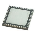
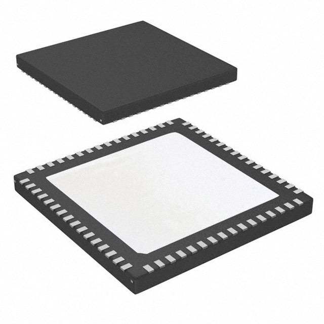
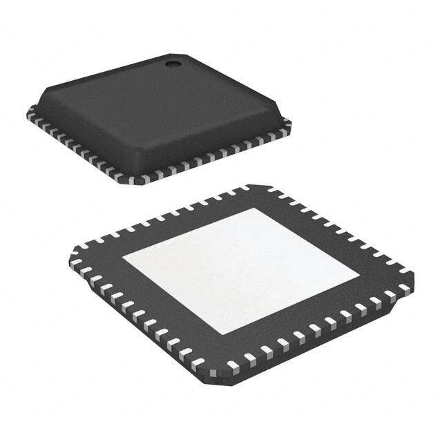
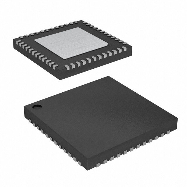
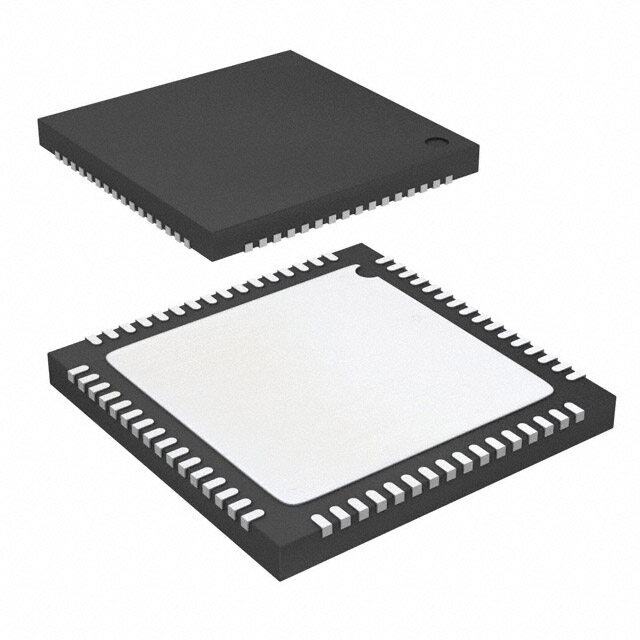
| 封装/外壳 | 48-VFQFN 裸露焊盘 |
| 工作温度 | -40°C ~ 85°C |
| 工作电源电压 | 2.1 V to 3.6 V |
| 工厂包装数量 | 2000 |
| 应用 | - |
| 数据接口 | PCB,表面贴装 |
| 数据速率(最大值) | 250kbps |
| 最大工作温度 | + 85 C |
| 最小工作温度 | - 40 C |
| 标准包装 | 1 |
| 灵敏度 | -100dBm |
| 电压-电源 | 2.1 V ~ 3.6 V |
| 电流-传输 | 31mA |
| 电流-接收 | 26mA |
| 系列 | EM351 |
| 调制或协议 | 802.15.4 Zigbee |
| 频率 | 2.4GHz |


- 商务部:美国ITC正式对集成电路等产品启动337调查
- 曝三星4nm工艺存在良率问题 高通将骁龙8 Gen1或转产台积电
- 太阳诱电将投资9.5亿元在常州建新厂生产MLCC 预计2023年完工
- 英特尔发布欧洲新工厂建设计划 深化IDM 2.0 战略
- 台积电先进制程称霸业界 有大客户加持明年业绩稳了
- 达到5530亿美元!SIA预计今年全球半导体销售额将创下新高
- 英特尔拟将自动驾驶子公司Mobileye上市 估值或超500亿美元
- 三星加码芯片和SET,合并消费电子和移动部门,撤换高东真等 CEO
- 三星电子宣布重大人事变动 还合并消费电子和移动部门
- 海关总署:前11个月进口集成电路产品价值2.52万亿元 增长14.8%

PDF Datasheet 数据手册内容提取
EM351/EM357 High-Performance, Integrated ZigBee/802.15.4 System-on-Chip Features Exceptional RF Performance - 32-bit ARM® Cortex -M3 processor - Normal mode link budget up to 103 dB; configurable up s - 2.4 GHz IEEE 802.15.4-2003 transceiver & lower MAC to 110 dB - 128 or 192 kB flash, with optional read protection - –100 dBm normal RX sensitivity; configurable to n - 12 kB RAM memory –102 dBm (1% PER, 20 byte packet) - AES128 encryption accelerator - +3 dB normal mode output power; configurable up tog - Flexible ADC, UART/SPI/TWI serial communications, +8 dBm i and general purpose timers - Robust Wi-Fi and Bluetooth coexistence s - 24 highly configurable GPIOs with Schmitt trigger inputs Innovative network and processor deebug Industry-leading ARM® Cortex -M3 processor - Packet Trace Port for non-intrusive packet trace with D - Leading 32-bit processing performance Ember development tools - Highly efficient Thumb-2 instruction set - Serial Wire/JTAG interface - Operation at 6, 12, or 24 MHz - Standard ARM debug capabwilities: Flash Patch & Break- - Flexible Nested Vectored Interrupt Controller point; Data Watchpoint & Trace; Instrumentation Trace Macrocell Low power consumption, advanced management e Application Flexibility - RX Current (w/ CPU): 26 mA N - Single voltage operation: 2.1–3.6 V with internal 1.8 and - TX Current (w/ CPU, +3 dBm TX): 31 mA 1.25 V regulators - Low deep sleep current, with retained RAM and GPIO: - Optional 32 .768 kHz crystal for higher timer accuracy 400 nA without/800 nA with sleep timer r - Low external component count with single 24 MHz - Low-frequency internal RC oscillator for low-power sleep o crystal timing - High-frequency internal RC oscillator for fast (110 µs) - Sfupport for external power amplifier - Small 7x7 mm 48-pin QFN package processor start-up from sleep d e d PA select n TX_ACTIVE Data Program RAM Flash RF_TX_ALT_P,N PA 12 kB 128/192 kB e SYNTH DAC MAC PA m + RF_P,N LNA IF ADC Baseband ARM® CortexTM-M3 2nd level CPU with NVIC Interrupt and MPU controller m Bias Packet Trace CPU debug OSCA oHF crystal Internal HF Calibration TPIU/ITM/ Eancccrleyrpatitoonr OSCB OSC RC-OSC ADC General FPB/DWT c purpose 1.25V timers Always VDD_COeRE Regulator Powered Serial SWCLK, Domain VRREG_OUT 1.8V GPIO Wire and JTCK Regulator registers JTAG Watchdog debug General nRESET POR Purpose t ADC UART/ o LF crystal Internal LF SPI/TWI Chip Sleep OSC RC-OSC manager timer N GPIO multiplexor switch PA[7:0], PB[7:0], PC[7:0] Rev 1.3 8/13 Copyright © 2013 by Silicon Laboratories EM351/EM357
s n g i s e D w e N r o f d e d n e m m o c e R t o N 2 Rev 1.3
Table of Contents 1. Typical Application..............................................................................................................5 2. Electrical Specifications......................................................................................................8 s 2.1. Absolute Maximum Ratings............................................................................................8n 2.2. Recommended Operating Conditions............................................................................8 g 2.3. Environmental Characteristics........................................................................................9 2.4. DC Electrical Characteristics................................................................................i..........9 s 2.5. Digital I/O Specifications..............................................................................................14 e 2.6. Non-RF System Electrical Characteristics...................................................................15 2.7. RF Electrical Characteristics...................................................................D.....................16 3. Functional Description......................................................................................................22 4. Radio Module.....................................................................................................................25 w 4.1. Receive (RX) Path........................................................................................................25 4.2. Transmit (TX) Path.................................................................e......................................25 4.3. Calibration....................................................................................................................25 N 4.4. Integrated MAC Module...............................................................................................26 4.5. Packet Trace Interface (PTI)........................................................................................26 4.6. Random Number Generator...................................r......................................................26 o 5. ARM® Cortex™-M3 and Memory Modules......................................................................27 5.1. ARM® Cortex™-M3 Microprocessor.............f...............................................................27 5.2. Embedded Memory......................................................................................................27 d 5.3. Memory Protection Unit................................................................................................34 6. System Modules......................................e...........................................................................35 6.1. Power Domains............................d................................................................................36 6.2. Resets..........................................................................................................................37 n 6.3. Clocks...........................................................................................................................40 6.4. System Timers.................e............................................................................................45 6.5. Power Management....m.................................................................................................46 6.6. Security Accelerator.....................................................................................................49 7. GPIO (General Purpomse Input/Output).............................................................................50 7.1. GPIO Ports...................................................................................................................51 7.2. Configuration................................................................................................................51 o 7.3. Forced Functions..........................................................................................................52 c 7.4. Reset............................................................................................................................53 e 7.5. Boot Configuration........................................................................................................53 7.6. GRPIO Modes.................................................................................................................54 7.7. Wake Monitoring..........................................................................................................55 7. 8. External Interrupts........................................................................................................55 t 7.9. Debug Control and Status............................................................................................56 o 7.10.GPIO Signal Assignment Summary.............................................................................57 N 7.11.Registers......................................................................................................................58 8. Serial Controllers...............................................................................................................70 8.1. Overview......................................................................................................................70 8.2. Configuration................................................................................................................71 8.3. SPI - Master Mode.......................................................................................................76 Rev 1.3 3
8.4. SPI - Slave Mode.........................................................................................................84 8.5. TWI - Two Wire serial Interfaces..................................................................................87 8.6. UART - Universal Asynchronous Receiver / Transmitter.............................................93 s 8.7. DMA Channels...........................................................................................................101 9. General Purpose Timers (TIM1 and TIM2).....................................................................114n 9.1. Introduction.................................................................................................................114 g 9.2. GPIO Usage...............................................................................................................116 i 9.3. Timer Functional Description..............................................................................s........116 9.4. Interrupts....................................................................................................................144 e 9.5. Registers....................................................................................................................145 D 10.ADC (Analog to Digital Converter).................................................................................172 10.1.Setup and Configuration............................................................................................173 10.2.Interrupts.......................................................................................w.............................176 10.3.Operation...................................................................................................................177 10.4.Calibration..............................................................................e....................................178 10.5.ADC Key Parameters.................................................................................................179 N 10.6.Registers....................................................................................................................183 11.Interrupt System............................................................ ..................................................190 r 11.1.Nested Vectored Interrupt Controller (NVIC).............................................................190 o 11.2.Event Manager...........................................................................................................192 11.3.Non-Maskable Interrupt (NMI)......................f.............................................................195 11.4.Faults.........................................................................................................................195 d 11.5.Registers....................................................................................................................196 e 12.Trace Port Interface Unit (TPIU)......................................................................................203 13.Instrumentation Trace Macrocell (ITdM)..........................................................................204 14.Data Watchpoint and Trace (DWT).................................................................................205 n 15.Flash Patch and Breakpoint (FPB).................................................................................206 e 16.Integrated Voltage Regulator..........................................................................................207 17.Serial Wire and JTAG (SWmJ) Interface...........................................................................209 18.Ordering Information.......................................................................................................210 19.Pin Definitions..........m........................................................................................................211 19.1.Pin Definitions............................................................................................................211 20.Package............o................................................................................................................223 20.1.QFN48 Footprint Recommendations.........................................................................223 c 20.2.Solder Temperature Profile........................................................................................225 e 21.Top Marking......................................................................................................................227 22.ShippiRng Box Label.........................................................................................................228 Appendix A—Register Address Table.................................................................................229 Appendix B—Abbreviations and Acronyms.......................................................................235 t Aoppendix C—References.....................................................................................................239 Document Change List.........................................................................................................240 N Contact Information..............................................................................................................241 4 Rev 1.3
1. Typical Application Figure 1.1 illustrates the typical application circuit, and Table 1.1 contains an example bill of materials (BOM) for the off-chip components required by the EM35x. s Note: The circuit shown in Figure 1.1 is for example purposes only, and the BOM is for budgetary quotes only. For a complete n reference design, please download one of the latest Ember Hardware Reference Designs from the Silicon Labs website (www.silabs.com/zigbee-support). g The Balun provides an impedance transformation from the antenna to the EM35x for both TX and RX modes. i L1 tunes the impedance presented to the RF port for maximum transmit power and receive sensitivity. s The harmonic filter (L2, L3, C5, C6 and C9) provides additional suppression of the second haermonic, which increases the margin over the FCC limit. D The 24 MHz crystal Y1 with loading capacitors is required and provides the high-frequency crystal oscillator source for the EM35x's main system clock. The 32.768 kHz crystal with loading capacitors generates a highly accurate low-frequency crystal oscillator for use with peripherals, but it is not mandatory as thew low-frequency internal RC oscillator can be used. Loading capacitance and ESR (C1 and R3) provides stability for the internal 1.8 Ve regulator. Loading capacitance C2 provides stability for the internal 1.25 V regulatorN, no ESR is required because it is contained within the chip. Resistor R1 reduces the operating voltage of the flash memory, this re duces current consumption and improves sensitivity by 1 dB when compared to not using it. r o Various decoupling capacitors are required, these should be placed as close to their corresponding pins as possible. For values and locations see one of the latest referenfce designs. An antenna matched to 50 is required. d e d n e m m o c e R t o N Rev 1.3 5
C3 Y1 C4 s n R1 VBRD g i s e 484746454443424140393837 Antenna Ceramic 123 VVDDDD__2V4CMOHz OSCAOSCBVDD_SYNTHVDD_PREVDD_COREPB5PB6PB7PC0VDD_MEMPC1VDD_PADS DPPBC04 333546 RF_P w PC3 EM35x Balun 33 PC2 L1 L3 L2 C e JTCK 32 D 4 31 RF_N PB2 N 5 30 VDD_RF PB1 6 RF_TX_ALT_P 7 29 C9 C5 C6 8 RF_TX_ALT_N PA6 VDD_IF r 28 Harmonic 9 NC o VDD_PADS 27 Filter f PA5 10 VDD_ PADSA PA4 26 e1112 PndRCE5SET PC6PC7VREG_OUTVDD_PADSVDD_COREPA7PB3PB4PA0PA1VDD_PADSPA2 GPNAD3 4295 131415161718192021222324 d n C7 e m C2 Optional Y2 m C8 o PC2 c PC0 PC3 e R3 JTCK Programing and PC4 debug interface R nReset (these pins should be C1 PA4 routed to test points) PA5 t o Figure 1.1. Typical Application Circuit N 6 Rev 1.3
Table 1.1 contains a typical Bill of Materials for the application circuit shown in Figure 1.1. The information within this table should be used for a rough cost analysis. For a more detailed BOM, please refer to one of Ember EM35x- based reference designs at the Silicon Labs website (www.silabs.com/zigbee-support). s Table 1.1. Bill of Materials for Typical Application Circuit n Item Qty Reference Description Manufacturer g 1 1 C2 CAPACITOR, 1 µF, 6.3 V, X5R, 10%, 0402 <not specifieid> s 2 1 C1 CAPACITOR, 2.2 µF, 10 V, X5R, 10%, 0603 <not specified> e 3 1 C7 CAPACITOR, 22 pF, ±5%, 50 V, NPO, 0402 <not specified> D 4 2 C3,C4 CAPACITOR, 18 pF, ±5%, 50 V, NPO, 0402 <not specified> w 5 1 C8 CAPACITOR, 33 pF, ±5%, 50 V, NPO, 0402 <not specified> 6 2 C5, C9 CAPACITOR, 1 pF, ±0.25 pF, 50 V, 0402, NPOe <not specified> N 7 1 C6 CAPACITOR, 1.8 pF, ±0.25 pF, 50 V, 0402, NPO 8 1 L1 INDUCTOR, 5.1 nH, ±0.3 nH, 0402 M ULTILAYER Murata LQG15HS5N1 r 9 2 L2, L3 INDUCTOR, 2.7 nH, ±0.3 nH, 04o02, MULTILAYER Murata LQG15HS2N7 10 1 R1 RESISTOR, 10 Ωf, 5%, 0402 <not specified> d 11 1 R3 RESISTOR, 1 Ω, 5%, 0402 <not specified> e 12 1 U1 EM35x SINGLE-CHIP ZIGBEE/802.15.4-2003 Ember EM35x dSOLUTION 13 1 Y1 CRYSTALn, 24.000 MHz, ± 25 ppm STABILITY ILSI, Abracon, KDS, OVER –40 to +85 ºC, 18 pF Epson e m 14 1 Y2 (Optional) CRYSTAL, 32.768 kHz, ±20 ppm INITIAL TOLER- Abracon, KDS, Epson ANCE AT +25ºC, 12.5 pF m 15 1 BLN1 BALUN, CERAMIC 50/200 Ω Wurth 748421245 o Johanson 2450BL15B100E c Murata LDB212G4010C e 16 1 ANT1 ANTENNA Johanson R 2450AT18B100E t o N Rev 1.3 7
2. Electrical Specifications 2.1. Absolute Maximum Ratings s Table 2.1 lists the absolute maximum ratings for the EM35x. n Table 2.1. Absolute Maximum Ratings g Parameter Test Condition Min Max iUnit s Regulator input voltage (VDD_PADS) –0.3 +3.6 V e Analog, Memory and Core voltage (VDD_24MHZ, –0.3 +2.0 V D VDD_VCO, VDD_RF, VDD_IF, VDD_PADSA, VDD_MEM, VDD_PRE, VDD_SYNTH, VDD_CORE) Voltage on RF_P,N; RF_TX_ALT_P,N w–0.3 +3.6 V RF Input Power RX signal into a lossless — +15 dBm e (for max level for correct packet reception see balun Table 2.7) N Voltage on any GPIO (PA[7:0], PB[7:0], PC[7:0]), –0.3 VDD_PAD V SWCLK, nRESET, VREG_OUT S +0.3 r Voltage on any GPIO pin (PA4, PA5, PB5, PB6, PB7, o –0.3 2.0 V PC1), when used as an input to the general purpose f ADC d Voltage on OSCA, OSCB, NC –0.3 VDD_PAD V e SA +0.3 Storage temperature d –40 +140 °C Note: Exposure to absolute-maximum-rated condnitions for extended periods may affect device reliability. e 2.2. Recommended Operating Conditions m Table 2.2 lists the rated operating conditions of the EM35x. Table 2.2. Operating Condmitions Parameter Test Condition Min Typ Max Unit o Regulator input voltage (VDD_PADS) 2.1 — 3.6 V c Analog and memeory input voltage 1.7 1.8 1.9 V (VDD_24MHZ, VDD_VCO, VDD_RF, VDD_IF, VDD_PADSRA, VDD_MEM, VDD_PRE, VDD_SYNTH) Corte input voltage when supplied from internal 1.18 1.25 1.32 V reogulator (VDD_CORE) N Core input voltage when supplied externally 1.18 — 1.9 V (VDD_CORE) Operating temperature range, T –40 — +85 °C A Note: Exposure to absolute-maximum-rated conditions for extended periods may affect device reliability. Rev 1.3 8
2.3. Environmental Characteristics Table 2.3 lists the rated environmental characteristics of the EM35x. Table 2.3. Environmental Characteristics s n Parameter Symbol Test Condition Min Typ Max Unit g ESD (human body model) On any pin — — ±2 kV i ESD (charged device model) Non-RF pins — — ±400s V ESD (charged device model) RF pins — — ±2e25 V Package Thermal Resistance* 27.1 D °C/W JA *Note: Thermal resistance assumes multi-layer PCB with exposed pad soldered to a PCB board. w 2.4. DC Electrical Characteristics e Table 2.4 lists the dc electrical characteristics of the EM35x. N Table 2.4. DC Characteristics Measured on Silicon Labs’ EM357 reference design with T = 25 °C and V = 3 V, unless otherwise noted. A DD r Parameter Test Condition o Min Typ Max Unit Regulator input voltage 2.1 — 3.6 V f (VDD_PADS) d Power supply range (VDD_MEM) Regulator output or external input 1.7 1.8 1.9 V Power supply range (VDD_CORE) Reguelator output 1.18 1.25 1.32 V Deep Sleep Current d Quiescent current, internal RC –4n0 °C, VDD_PADS=3.6 V — 0.4 — A oscillator disabled +25 °C, VDD_PADS=3.6 V — 0.4 — A e +85 °C, VDD_PADS=3.6 V — 0.7 — A m Quiescent current, including –40 °C, VDD_PADS=3.6 V — 0.7 — A internal RC oscillator m +25 °C, VDD_PADS=3.6 V — 0.7 — A +85°C, VDD_PADS=3.6 V — 1.1 — A o Quiescent current, including –40 °C, VDD_PADS=3.6 V — 0.8 — A 32.768 kHz oscillatcor +25 °C, VDD_PADS=3.6 V — 1.0 — A e +85 °C, VDD_PADS=3.6 V — 1.5 — A Quiescent Rcurrent, including –40 °C, VDD_PADS=3.6 V — 1.1 — A internal RC oscillator and +25 °C, VDD_PADS=3.6 V — 1.3 — A 32.76 8 kHz oscillator t +85 °C, VDD_PADS=3.6 V — 1.8 — A o Simulated deep sleep (debug With no debugger activity — 300 — A N mode) current 9 Rev 1.3
Table 2.4. DC Characteristics (Continued) Measured on Silicon Labs’ EM357 reference design with T = 25 °C and V = 3 V, unless otherwise noted. A DD Parameter Test Condition Min Typ Max Unit s Reset Current n Quiescent current, nRESET Typ at 25 °C/3.0 V — 1.2 2.0 mA g asserted Max at 85 °C/3.6 V i Processor and Peripheral Currents s ARM® CortexTM-M3, RAM, and 25 °C, 1.8 V memory and — 6.5 —e mA flash memory 1.25 V core ARM® CortexTM-M3 running at 12 MHz D from crystal oscillator Radio and all peripherals off w ARM® CortexTM-M3, RAM, and 25 °C, 1.8 V memory and — 7.5 — mA flash memory 1.25 V core e ARM® CortexTM-M3 running at 24 MHz N from crystal oscillator Radio and all peripherals off ARM® CortexTM-M3, RAM, and 25 °C, 1.8 V memory andr — 3.0 — mA flash memory sleep current 1.25 V core o ARM® CortexTM-M3 sleeping, CPU f clock set to 12 MHz fr om the crystal oscilladtor Radio and all peripherals off e ARM® CortexTM-M3, RAM, and 25 °C, 1.8 V memory and — 2.0 — mA d flash memory sleep current 1.25 V core ARM®n CortexTM-M3 sleeping, CPU clock set to 6 MHz from the high fre- e quency RC oscillator m Radio and all peripherals off Serial controller current For each controller at maximum data — 0.2 — mA m rate General purpose timer current For each timer at maximum clock rate — 0.25 — mA o General purpose ADC current At maximum sample rate, DMA enabled — 1.1 — mA c RX Current Radio receiver,e MAC, and base- ARM® CortexTM-M3 sleeping, CPU — 22.0 — mA band R clock set to 12 MHz Total RX current ( = I receiver, 25 °C, VDD_PADS=3.0 V — 25.5 — mA Radio MAC and baseband, CPU + IRAM, ARM® CortexTM-M3 running at 12 MHz t and Flash memory ) o 25 °C, VDD_PADS=3.0 V — 26.5 — mA ARM® CortexTM-M3 running at 24 MHz N Boost mode total RX current ( = 25 °C, VDD_PADS=3.0 V — 27.5 — mA I receiver, MAC and base- ARM® CortexTM-M3 running at 12 MHz Radio band, CPU+ IRAM, and flash 25 °C, VDD_PADS=3.0 V — 28.5 — mA memory ) ARM® CortexTM-M3 running at 24 MHz Rev 1.3 10
Table 2.4. DC Characteristics (Continued) Measured on Silicon Labs’ EM357 reference design with T = 25 °C and V = 3 V, unless otherwise noted. A DD Parameter Test Condition Min Typ Max Unit s TX Current n Radio transmitter, MAC, and base- 25 °C and 1.8 V core; max. power out — 26.0 — mA g band (+3 dBm typical) ARM® CortexTM-M3 sleeping, CPU i s clock set to 12 MHz e Total TX current ( = I transmit- 25 °C, VDD_PADS=3.0 V; maximum — 42.5 — mA Radio ter, MAC and baseband, CPU + power setting (+8 dBm); ARM® D IRAM, and flash memory) CortexTM-M3 running at 12 MHz 25 °C, VDD_PADS=3.0 V; +3 dBm — 3 0.0 — mA power setting; ARM® CortexTM-M3 w running at 12 MHz e 25 °C, VDD_PADS=3.0 V; 0 dBm power — 27.5 — mA setting; ARM® CortexTM-M3 running at N 12 MHz 25 °C, VDD_PADS=3.0 V; minrimum — 21.5 — mA power setting; ARM® CorteoxTM-M3 running at 12 MHz f 25 °C, VDD_PADS=3 .0 V; maximum — 43.5 — mA power setting (+8 ddBm); ARM® Cor- texTM-M3 running at 24 MHz e 25 °C, VDD_PADS=3.0 V; +3 dBm — 31.0 — mA power settding; ARM® CortexTM-M3 nrunning at 24 MHz 25 °C, VDD_PADS=3.0 V; 0 dBm power — 28.5 — mA e setting; ARM® CortexTM-M3 running at m 24 MHz 25 °C, VDD_PADS=3.0 V; minimum — 22.5 — mA m power setting; ARM® CortexTM-M3 running at 24 MHz o c e R t o N 11 Rev 1.3
Figure 2.1 shows the variation of current in transmit mode (with the ARM® CortexTM-M3 running at 12 MHz). s n g i s e D w e N r o f d e d n Figure 2.1. Transmit Power Consumption e m m o c e R t o N Rev 1.3 12
Figure 2.2 shows typical output power against power setting on the Silicon Labs reference design. s n g i s e D w e N r o f d e d n Figure 2.2. Transmit Output Power e m m o c e R t o N 13 Rev 1.3
2.5. Digital I/O Specifications Table 2.5 lists the digital I/O specifications for the EM35x. The digital I/O power (named VDD_PADS) comes from three dedicated pins (pins 23, 28 and 37). The voltage applied to these pins sets the I/O voltage. s Table 2.5. Digital I/O Specifications n Parameter Test Condition Min Typ Max Unit g Voltage supply (regulator input voltage) 2.1 — 3.6 V i Low Schmitt switching threshold VSWIL 0.42 x — 0.50 x s V Schmitt input threshold going VDD_PADS VDD_PADS e from high to low High Schmitt switching threshold V 0.62 x — D0.80 x V SWIH Schmitt input threshold going VDD_PADS VDD_PADS from low to high w Input current for logic 0 I — — –0.5 μA IL Input current for logic 1 I —e — +0.5 μA IH Input pull-up resistor value RIPU N24 29 34 k Input pull-down resistor value R 24 29 34 k IPD Output voltage for logic 0 V 0 — 0.18 x V OL r (IOL = 4 mA for standard poads, VDD_PADS 8 mA for high current pads) f Output voltage for logic 1 VOH 0.82 x — VDD_PADS V (I = 4 mA for stdandard pads, VDD_PADS OH 8 mA for high current pads) e Output source current I — — 4 mA OHS d (standard current pad) Output sink current n I — — 4 mA OLS (standard current pad) e Output source current high current pad: I — — 8 mA OHH PA6, PA7, PB6, PB7, PC0 m Output sink current high current pad: I — — 8 mA OLH PA6, PA7, PB6, PB7, PC0 m Total output current (for I/O Pads) I + I — — 40 mA OH OL o c e R t o N Rev 1.3 14
Table 2.6 lists the nRESET pin specifications for the EM35x. The digital I/O power (named VDD_PADS) comes from three dedicated pins (pins 23, 28 and 37). The voltage applied to these pins sets the I/O voltage. Table 2.6. nReset Pin Specifications s Parameter Test Condition Min Typ Max Unit n Low Schmitt switching threshold V 0.42 x — 0.50 x gV SWIL Schmitt input threshold going from VDD_PADS VDD_PADS i high to low s High Schmitt switching threshold V 0.62 x — 0.80e x V SWIH Schmitt input threshold going from VDD_PADS VDD_PADS D low to high Input current for logic 0 I — — –0.5 μA IL w Input current for logic 1 I — — +0.5 μA IH e Input pull-up resistor value R 24 29 34 k IPU Pull-up value while the chip is not N reset Input pull-up resistor value RIPURESET r 12 14.5 17 k Pull-up value while the chip iso reset f 2.6. Non-RF System Electrical Characteristicsd Table 2.7 lists the non-RF system level characteristics efor the EM35x. d Table 2.7. Non-RF System Electrical Characteristics Measured on Silicon Labs’ EM357 reference designn with TA = 25 °C and VDD = 3 V, unless otherwise noted. Parameter e Test Condition Min Typ Max Unit System wake time from deep mFrom wakeup event to first ARM® Cor- — 110 — µs sleep texTM-M3 instruction running from 6 MHz m internal RC clock Includes supply ramp time and oscillator startup time o Shutdown time going into deep From last ARM® CortexTM-M3 instruction — 5 — µs c sleep to deep sleep mode e R t o N 15 Rev 1.3
2.7. RF Electrical Characteristics 2.7.1. Receive Table 2.8 lists the key parameters of the integrated IEEE 802.15.4-2003 receiver on the EM35x. s Receive measurements were collected with the Silicon Labs EM35x Ceramic Balun Reference Design (Version n A0) at 2440 MHz. The typical number indicates one standard deviation above the mean, measured at room temperature (25C). The min and max numbers were measured over process corners at room temperature. g i Table 2.8. Receive Characteristics s Parameter Test Condition Min Typ Meax Unit Frequency range 2400 — D2500 MHz Sensitivity (boost mode) 1% PER, 20 byte packet defined by — –102 –96 dBm IEEE 802.15.4-2003; w Sensitivity 1% PER, 20 byte packet defined by — –100 –94 dBm e IEEE 802.15.4-2003; N High-side adjacent channel rejection IEEE 802.15.4-2003 interferer signal, — 35 — dB wanted IEEE 802.15.4-2003 signal at –82 dBm r o Low-side adjacent channel rejection IEEE 802.15.4-2003 interferer signal, — 35 — dB wanted IEEE 802.15f.4-2003 signal at –82 dBm d 2nd high-side adjacent channel rejec- IEEE 802.15.4-2003 interferer signal, — 46 — dB tion wanted IEEeE 802.15.4-2003 signal at –82 dBm d 2nd low-side adjacent channel rejection IEEE 802.15.4-2003 interferer signal, — 46 — dB n wanted IEEE 802.15.4-2003 signal e at –82 dBm High-side adjacent channel rejectionm Filtered IEEE 802.15.4-2003 inter- — 39 — dB ferer signal, wanted IEEE 802.15.4- 2003 signal at –82 dBm m Low-side adjacent channel rejection Filtered IEEE 802.15.4-2003 inter- — 47 — dB o ferer signal, wanted IEEE 802.15.4- 2003 signal at –82 dBm c 2nd high-side adjacent channel Filtered IEEE 802.15.4-2003 inter- — 49 — dB e rejection ferer signal, wanted IEEE 802.15.4- R 2003 signal at –82 dBm 2nd low-side adjacent channel rejection Filtered IEEE 802.15.4-2003 inter- — 49 — dB t ferer signal, wanted IEEE 802.15.4- o 2003 signal at –82 dBm N High-side adjacent channel rejection CW interferer signal, wanted IEEE — 44 — dB 802.15.4-2003 signal at –82 dBm Low-side adjacent channel rejection CW interferer signal, wanted IEEE — 47 — dB 802.15.4-2003 signal at –82 dBm Rev 1.3 16
Table 2.8. Receive Characteristics (Continued) Parameter Test Condition Min Typ Max Unit 2nd high-side adjacent channel CW interferer signal, wanted IEEE — 59 — dB s rejection 802.15.4-2003 signal at –82 dBm n 2nd low-side adjacent channel rejection CW interferer signal, wanted IEEE — 59 — dgB 802.15.4-2003 signal at –82 dBm i s Channel rejection for all other channels IEEE 802.15.4-2003 interferer signal, — 40 — dB wanted IEEE 802.15.4-2003 signal e at –82 dBm D 802.11g rejection centered at +12 MHz IEEE 802.15.4-2003 interferer signal, — 36 — dB or –13 MHz wanted IEEE 802.15.4-2003 signal at –82 dBm w Maximum input signal level for correct 0 — — dBm e operation N Co-channel rejection IEEE 802.15.4-2003 interferer signal, — –6 — dBc wanted IEEE 802.15.4-2003 signal at –82 dBm r Relative frequency error o –120 — +120 ppm (50% greater than the 2x40 ppm f required by IEEE 802.15.4-2003) d Relative timing error –120 — +120 ppm (50% greater than the 2x40 ppm e required by IEEE 802.15.4-2003) d Linear RSSI range As defined by IEEE 802.15.4-2003 40 — — dB n RSSI Range –90 — –40 dBm e m m o c e R t o N 17 Rev 1.3
Figure 2.3 shows the variation of receive sensitivity with temperature for boost mode and normal mode for a typical chip. s n g i s e D w e N r o f d e d n Figure 2.3.e Receive Sensitivity vs. Temperature m m o c e R t o N Rev 1.3 18
2.7.2. Transmit Table 2.9 lists the key parameters of the integrated IEEE 802.15.4-2003 transmitter on the EM35x. Transmit measurements were collected with the Silicon Labs EM35x Ceramic Balun Reference Design (Version s A0) at 2440 MHz. The Typical number indicates one standard deviation below the mean, measured at room temperature (25C). The Min and Max numbers were measured over process corners at room temperature. Inn terms of impedance, this reference design presents a 3n3 inductor in parallel with a 100:50 Ω balun to the RF pins. g Table 2.9. Transmit Characteristics i s Parameter Test Condition Min Typ Max Unit e Maximum output power At highest boost mode power setting (+8) — 8 — dBm D (boost mode) Maximum output power At highest normal mode power setting (+3) 1 5 — dBm w Minimum output power At lowest power setting — –55 — dBm Error vector magnitude As defined by IEEE 802.15.4-2003, e— 5 15 % (Offset-EVM) which sets a 35% maximum N Carrier frequency error –40 — +40 ppm PSD mask relative 3.5 MHz away r –20 — — dB o PSD mask absolute 3.5 MHz away –30 — — dBm f d e d n e m m o c e R t o N 19 Rev 1.3
Figure 2.4 shows the variation of transmit power with temperature for maximum boost mode power, and normal mode for a typical chip. s n g i s e D w e N r o f d e d n Figure 2.e4. Transmit Power vs. Temperature m m o c e R t o N Rev 1.3 20
2.7.3. Synthesizer Table 2.10 lists the key parameters of the integrated synthesizer on the EM35x. Table 2.10. Synthesizer Characteristics s Measured on Silicon Labs’ EM357 reference design with T = 25 °C and V = 3 V, unless otherwise noted. A DD n Parameter Test Condition Min Typ Max Ungit Frequency range 2400 — 2500 iMHz s Frequency resolution — 11.7 — kHz e Lock time From off — — 100 μs D Relock time Channel change or RX/TX turnaround — — 100 μs (IEEE 802.15.4-2003 defines 192 μs turnaround time) w Phase noise at 100 kHz offset — –75 — dBc/Hz e Phase noise at 1 MHz offset — –100 — dBc/Hz N Phase noise at 4 MHz offset — –108 — dBc/Hz Phase noise at 10 MHz offset r — –114 — dBc/Hz o f d e d n e m m o c e R t o N 21 Rev 1.3
3. Functional Description The EM351 and EM357 are fully integrated system-on-chips that integrate a 2.4 GHz, IEEE 802.15.4-2003- compliant transceiver, 32-bit ARM® Cortex-M3 microprocessor, flash and RAM memory, and peripherals of use to s designers of ZigBee-based systems. n The transceiver uses an efficient architecture that exceeds the dynamic range requirements imposed by the IEEE 802.15.4-2003 standard by over 15 dB. The integrated receive channel filtering allows for robust co-existenceg with other communication standards in the 2.4 GHz spectrum, such as IEEE 802.11-2007 and Bluetooth. The integrated i regulator, VCO, loop filter, and power amplifier keep the external component count low. An opstional high performance radio mode (boost mode) is software-selectable to boost dynamic range. e The integrated 32-bit ARM® Cortex-M3 microprocessor is highly optimized for high performance, low power consumption, and efficient memory utilization. Including an integrated MPU, it supports two Ddifferent modes of operation—privileged mode and user mode. This architecture could allow for separation of the networking stack from the application code, and prevents unwanted modification of restricted areas o f memory and registers w resulting in increased stability and reliability of deployed solutions. The EM351 has 128 kB of embedded flash memory and the EM357 has 192 kB of embedded flash memory. Both e chips have 12 kB of integrated RAM for data and program storage. The Ember software for the EM35x employs an effective wear-leveling algorithm that optimizes the lifetime of the embedded fNlash. To maintain the strict timing requirements imposed by the ZigBee and IEEE 802.15.4-2003 standards, the EM35x integrates a number of MAC functions, AES128 encryption accelerat or, and automatic CRC handling into the r hardware. The MAC hardware handles automatic ACK transmission and reception, automatic backoff delay, and o clear channel assessment for transmission, as well as automatic filtering of received packets. The Ember Packet Trace Interface is also integrated with the MAC, allowing complfete, non-intrusive capture of all packets to and from the EM35x with Ember development tools. d The EM35x offers a number of advanced power management features that enable long battery life. A high- frequency internal RC oscillator allows the processor ecore to begin code execution quickly upon waking. Various deep sleep modes are available with less than 1 µA power consumption while retaining RAM contents. To support d user-defined applications, on-chip peripherals include UART, SPI, TWI, ADC, and general-purpose timers, as well as up to 24 GPIOs. Additionally, an integranted voltage regulator, power-on-reset circuit, and sleep timer are available. e Finally, the EM35x utilizes standard Serial Wire and JTAG interfaces for powerful software debugging and programming of the ARM Cortex-Mm3 core. The EM35x integrates the standard ARM system debug components: Flash Patch and Breakpoint (FPB), Data Watchpoint and Trace (DWT), and Instrumentation Trace Macrocell (ITM). Target applications for the EM3m5x include the following: Smart Energy Building automaotion and control Home automation and control c Security and monitoring e General ZigBee wireless sensor networking R The technical data sheet details the EM35x features available to customers using it with Ember software. t o N Rev 1.3 22
Figure 3.1 shows a detailed block diagram of the EM35x. PA select TX_ACTIVE Data Program s RAM Flash RF_TX_ALT_P,N PA 12 kB 128/192 kB n SYNTH DAC MAC PA + g RF_P,N LNA IF ADC Baseband ARM® CortexTM-M3 2nd level CPU with NVIC Interrupt i and MPU controller s Bias Packet Trace e CPU debug OSCA HF crystal Internal HF Calibration TPIU/ITM/ EancccrleyrDpatitoonr OSCB OSC RC-OSC ADC General FPB/DWT purpose 1.25V timers Always VDD_CORE Regulator Powered w Serial SWCLK, Domain VREG_OUT 1.8V GPIO Wire and JTCK Regulator registers Watchdeog dJeTbAuGg General nRESET POR Purpose N ADC UART/ LF crystal Internal LF SPI/TWI Chip Sleep OSC RC-OSC manager timer r o GPIO multiplexor switch f d PA[7:0], PB[7:0], PC[7:0] e Figure 3.1. EM35x Block Diagram d The EM35x radio receiver is a low-IF, super-heterodyne receiver. The architecture has been chosen to optimize co- n existence with other devices in the 2.4 GHz band (namely Wi-Fi and Bluetooth), and to minimize power consumption. The receiver uses differenteial signal paths to reduce sensitivity to noise interference. Following RF amplification, the signal is downconverted by an image-rejecting mixer, filtered, and then digitized by an ADC. m The digital section of the receiver uses a coherent demodulator to generate symbols for the hardware-based MAC. The digital receiver also contains the analog radio calibration routines, and controls the gain within the receiver m path. The radio transmitter uses an efficient architecture in which the data stream directly modulates the VCO frequency. An integrated PA providoes the output power. Digital logic controls TX path and output power calibration. If the EM35x is to be used with an external PA, use the TX_ACTIVE or nTX_ACTIVE signal to control the timing of the c external switching logic. e The integrated 4.8 GHz VCO and loop filter minimize off-chip circuitry. Only a 24 MHz crystal with its loading capacitors isR required to establish the PLL local oscillator signal. The MAC interfaces the on-chip RAM to the RX and TX baseband modules. The MAC provides hardware-based IEEE 802.15.4-2003 packet-level filtering. It supplies an accurate symbol time base that minimizes the t synchronization effort of the Ember software and meets the protocol timing requirements. In addition, it provides o timer and synchronization assistance for the IEEE 802.15.4-2003 CSMA-CA algorithm. NThe EM35x integrates hardware support for a packet trace module, which allows robust packet-based debug. This element is a critical component of Ember Desktop, the Ember development environment, and provides advanced network debug capability when used with the Ember Debug Adapter (ISA3). The EM35x integrates an ARM® CortexTM-M3 microprocessor, revision r1p1. This industry-leading core provides 32-bit performance and is very power-efficient. It has excellent code density using the ARM® Thumb-2 instruction set. The processor can be operated at 12 or 24 MHz when using the high-frequency crystal oscillator, or at 6 MHz 23 Rev 1.3
or 12 MHz when using the high-frequency internal RC oscillator. The EM351 has 128 kB of flash memory and the EM357 has 192 kB of flash memory. Both chips have 12 kB of RAM on-chip, and the ARM configurable memory protection unit (MPU). s The EM35x implements both the ARM Serial Wire and JTAG debug interfaces. These interfaces provide real time, non-intrusive programming and debugging capabilities. Serial Wire and JTAG provide the same functionality, bunt are mutually exclusive. The Serial Wire interface uses two pins; the JTAG interface uses five. Serial Wire is g preferred, since it uses fewer pins. The EM35x contains 24 GPIO pins shared with other peripheral or alternate functions. Because of flexibile routing s within the EM35x, external devices can use the alternate functions on a variety of different GPIOs. The integrated serial controller SC1 can be configured for SPI (master or slave), TWI (master-only), or UART opeeration, and the serial controller SC2 can be configured for SPI (master or slave) or TWI (master-only) operation. D The EM35x has a general purpose ADC which can sample analog signals from six GPIO pins in single-ended or differential modes. It can also sample the 1.8 V regulated supply VDD_PADSA, the voltage reference VREF, and GND. The ADC has one voltage range: 0 to 1.2 V (normal). The ADC has a DMA modwe to capture samples and automatically transfer them into RAM. The integrated voltage reference for the ADC, VREF, can be made available to external circuitry. An external voltage reference can also be driven into the ADeC. The regulator input voltage, VDD_PADS, cannot be measured using the general purpose ADC, but it can be measured through Ember software. N The EM35x contains four oscillators: a high-frequency 24 MHz external crystal oscillator, a high-frequency 12 MHz internal RC oscillator, an optional low-frequency 32.768 kHz external crystal oscillator, and a low-frequency 10 kHz r internal RC oscillator. o The EM35x has an ultra low power, deep sleep state with a choice of clocking modes. The sleep timer can be f clocked with either the external 32.768 kHz crystal oscillator or with a 1 kHz clock derived from the internal 10 kHz RC oscillator. Alternatively, all clocks can be disabled for thde lowest power mode. In the lowest power mode, only external events on GPIO pins will wake up the chip. The EM35x has a fast startup time (typically 110 µs) from deep sleep to the execution of the first ARM® CortexTM-M3 ienstruction. The EM35x contains three power domains. The adlways-on high voltage supply powers the GPIO pads and critical chip functions. Regulated low voltage supplies power the rest of the chip. The low voltage supplies are disabled n during deep sleep to reduce power consumption. Integrated voltage regulators generate regulated 1.25 V and 1.8 V voltages from an unregulated supply voltage. The 1.8 V regulator output is decoupled and routed externally e to supply analog blocks, RAM, and flash memories. The 1.25 V regulator output is decoupled externally and supplies the core logic. m Note: The EM35x is not pin-compatible with the previous generation chip, the EM250, except for the RF section of the chip. Pins 1-11 and 45-48 are commpatible, to ease migration to the EM35x. o c e R t o N Rev 1.3 24
4. Radio Module The radio module consists of an analog front end and digital baseband as shown in Figure 3.1 on page 23. s 4.1. Receive (RX) Path n The RX path uses a low-IF, super-heterodyne receiver that rejects the image frequency using complex mixing and polyphase filtering. In the analog domain, the input RF signal from the antenna is first amplified and mixed dowgn to a 4 MHz IF frequency. The mixers’ output is filtered, combined, and amplified before being sampled by a 12 MSPS ADC. The digitized signal is then demodulated in the digital baseband. The filtering within the RX path iimproves s the EM35x’s co-existence with other 2.4 GHz transceivers such as Zigbee/ 802.15.4-2003, IEEE 802.11-2007, and Bluetooth radios. The digital baseband also provides gain control of the RX path, both to enable thee reception of small and large wanted signals and to tolerate large interferers. D 4.1.1. RX Baseband The EM35x RX digital baseband implements a coherent demodulator for optimal perfo rmance. The baseband w demodulates the O-QPSK signal at the chip level and synchronizes with the IEEE 802.15.4-2003-defined preamble. An automatic gain control (AGC) module adjusts the analog gain continuously every ¼ symbol until the e preamble is detected. Once detected, the gain is fixed for the remainder of the packet. The baseband despreads the demodulated data into 4-bit symbols. These symbols are buffered and passed to the hardware-based MAC N module for packet assembly and filtering. In addition, the RX baseband provides the calibration and control interfac e to the analog RX modules, including the LNA, RX baseband filter, and modulation modules. The Ember softwrare includes calibration algorithms that use this interface to reduce the effects of silicon process and temperatuore variation. 4.1.2. RSSI and CCA f The EM35x calculates the RSSI over every 8-symbol period as well as at the end of a received packet. The linear d range of RSSI is specified to be at least 40 dB over temperature. At room temperature, the linear range is approximately 60 dB (–90 dBm to –30 dBm input signael). The EM35x RX baseband provides support for the IEEE 802.15.4-2003 RSSI CCA method. Clear channel reports d busy medium if RSSI exceeds its threshold. n 4.2. Transmit (TX) Path e The EM35x TX path produces an O-QPSK-modulated signal using the analog front end and digital baseband. The area- and power-efficient TX architmecture uses a two-point modulation scheme to modulate the RF signal generated by the synthesizer. The modulated RF signal is fed to the integrated PA and then out of the EM35x. 4.2.1. TX Baseband m The EM35x TX baseband in the digital domain spreads the 4-bit symbol into its IEEE 802.15.4-2003-defined 32- chip sequence. It also provides the interface for the Ember software to calibrate the TX module to reduce silicon o process, temperature, and voltage variations. c 4.2.2. TX_ACTIVE and nTX_ACTIVE Signals For applicationse requiring an external PA, two signals are provided called TX_ACTIVE and nTX_ACTIVE. These signals are the inverse of each other. They can be used for external PA power management and RF switching R logic. In transmit mode the TX baseband drives TX_ACTIVE high, as described in Table 7.5 on page 57. In receive mode the TX_ACTIVE signal is low. TX_ACTIVE is the alternate function of PC5, and nTX_ACTIVE is the alternate functtion of PC6. See "7. GPIO (General Purpose Input/Output)" on page 50 for details of the alternate GPIO funoctions. The digital I/O that provide these signals have a 4 mA output sink and source capability. N4.3. Calibration The Ember software calibrates the radio using dedicated hardware resources. Rev 1.3 25
4.4. Integrated MAC Module The EM35x integrates most of the IEEE 802.15.4-2003 MAC requirements in hardware. This allows the ARM® CortexTM-M3 CPU to provide greater bandwidth to application and network operations. In addition, the hardware s acts as a first-line filter for unwanted packets. The EM35x MAC uses a DMA interface to RAM to further reduce the overall ARM® CortexTM-M3 CPU interaction when transmitting or receiving packets. n When a packet is ready for transmission, the Ember software configures the TX MAC DMA by indicating the packet g buffer RAM location. The MAC waits for the backoff period, then switches the baseband to TX mode and performs channel assessment. When the channel is clear the MAC reads data from the RAM buffer, calculates the CiRC, and s provides 4-bit symbols to the baseband. When the final byte has been read and sent to the baseband, the CRC remainder is read and transmitted. e The MAC is in RX mode most of the time. In RX mode various format and address filters keep unwanted packets D from using excessive RAM buffers, and prevent the CPU from being unnecessarily interrupted. When the reception of a packet begins, the MAC reads 4-bit symbols from the baseband and calculates the CRC. It then assembles the received data for storage in a RAM buffer. RX MAC DMA provides direct access to RwAM. Once the packet has been received additional data, which provides statistical information on the packet to the Ember software, is appended to the end of the packet in the RAM buffer space. e The primary features of the MAC are as follows: N CRC generation, appending, and checking Hardware timers and interrupts to achieve the MAC symbol timin g Automatic preamble and SFD pre-pending on TX packets r o Address recognition and packet filtering on RX packets Automatic acknowledgment transmission f Automatic transmission of packets from memory d Automatic transmission after backoff time if channel is clear (CCA) e Automatic acknowledgment checking Time stamping received and transmitted mdessages Attaching packet information to received packets (LQI, RSSI, gain, time stamp, and packet status) n IEEE 802.15.4-2003 timing and slotted/unslotted timing e 4.5. Packet Trace Interface (PTI) m The EM35x integrates a true PHY-level PTI for effective network-level debugging. It monitors all the PHY TX and RX packets between the MAC and baseband modules without affecting their normal operation. It cannot be used to inject packets into the PHY/MmAC interface. This 500 kbps asynchronous interface comprises the frame signal (PTI_EN, PA4) and the data signal (PTI_DATA, PA5). PTI is supported by the Ember development tools. o 4.6. Random Number Generator c Thermal noise in the analog circuitry is digitized to provide entropy for a true random number generator (TRNG). The TRNG prodeuces 16-bit uniformly distributed numbers. The Ember software uses the TRNG to seed a pseudo random number generator (PRNG). The TRNG is also used directly for cryptographic key generation. R t o N 26 Rev 1.3
® 5. ARM Cortex™-M3 and Memory Modules This chapter discusses the ARM® CortexTM-M3 Microprocessor, and reviews the EM35x’s flash and RAM memory modules as well as the Memory Protection Unit (MPU). s ® n 5.1. ARM Cortex™-M3 Microprocessor g The EM35x integrates the ARM® CortexTM-M3 microprocessor, revision r1p1, developed by ARM Ltd., making the EM35x a true System-on-Chip solution. The ARM® CortexTM-M3 is an advanced 32-bit modifiedi Harvard s architecture processor that has separate internal program and data buses, but presents a unified program and data address space to software. The word width is 32 bits for both the program and data sides. The ARMe® CortexTM-M3 allows unaligned word and half-word data accesses to support efficiently-packed data structures. D The ARM® CortexTM-M3 clock speed is configurable to 6 , 12 , or 24 MHz. For normal operation 24 MHz is preferred over 12 MHz due to improved performance for all applications and improved duty cycling for applications using sleep modes. The 6 MHz operation can only be used when radio operations are nwot required since the radio requires an accurate 12 MHz clock. The ARM® CortexTM-M3 in the EM35x has also been enhanced to support two sepearate memory protection levels. Basic protection is available without using the MPU, but normal operation uses the MPU. The MPU allows for N protecting unimplemented areas of the memory map to prevent common software bugs from interfering with software operation. The architecture could also allow for separation of the networking stack from the application code using a fine granularity RAM protection module. Errant writes are captured and details are reported to the r developer to assist in tracking down and fixing issues. o 5.2. Embedded Memory f Figure 5.1 shows the EM351 ARM® CortexTM-M3 memory m ap and Figure 5.2 shows the EM357 ARM® CortexTM- d M3 memory map. e d n e m m o c e R t o N Rev 1.3 27
0xE00FFFFF ROM table 0xE00FF000 Not used 0xE0042000 s Not used 0xE0041000 Not used TPIU n 0xE0040000 Private periph bus (externagl) 0xE003FFFF Not used Private periph bus (internal) 0xE000F000 NVIC i 0xE000E000 s Not used 0xE0003000 e FPB 0xE0002000 DWT D 0xE0001000 ITM Not used 0xE0000000 w 0x42002XXX e Register bit band alias region N mapped onto System interface (not used) r 0x42000000 o Not used 0x40000XXX Registers mapped onto Sysftem interface 0x40000000 d 0x22002000 e RAM bit band dalias region mapped onto System Peripheral n interface (not used) e 0x22000000 0xm20002FFF RAM (12kB) mapped onto System RAM interface 0x20000000 m 0x08040FFF Customer Info Block (2kB) o 00xx008800440078F0F0 Fixed Info Block (2kB) 0x08040000 Flash c 0x0801FFFF e Main Flash Block (128kB) R Upper mapping (Boot mode) t 0x08000000 o Optional boot mode 0x0001FFFF maps Fixed Info Block N Main Flash Block (128kB) to the start of memory Lower mapping 0x000007FF (Normal Mode) Fixed Info Block (2kB) 0x00000000 Figure 5.1. EM351 ARM® CortexTM-M3 Memory Map 28 Rev 1.3
0xE00FFFFF ROM table s 0xE00FF000 Not used 0xE0042000 n 0xFFFFFFFF Not used 0xE0041000 Not used TPIU g 0xE0040000 Private periph bus (external) 0xE003FFFF i 0xE000F000 Not used Private periph bus (internal) s0xE0000000 0xE000E000 NVIC e 0xDFFFFFFF Not used 0xE0003000 FPB D 0xE0002000 DWT 0xE0001000 ITM Not used 0xE0000000 w e 0x42002XXX Register bit band N 0xA0000000 alias region 0x9FFFFFFF mapped onto System interface (not used) r o 0x42000000 Not used 0x40000XXX Registers f mapped onto System interface d 0x40000000 e 0x22002000 0x60000000 RAM bit band 0x5FFFFFFF d alias region mapped onto System n Peripheral interface (not used) e 0x40000000 0x22000000 0x3FFFFFFF 0x20002FFFm RAM (12kB) mapped onto System RAM interface 0mx20000000 0x08040FFF 0x20000000 Customer Info Block (2kB) 0x1FFFFFFF 0x08040800 o 0x080407FF Fixed Info Block (2kB) 0x08040000 Flash c 0x0802FFFF e 0x00000000 Main Flash Block (192kB) R Upper mapping (Boot mode) 0x08000000 t o Optional boot mode 0x0002FFFF maps Fixed Info Block Main Flash Block (192kB) to the start of memory N Lower mapping 0x000007FF (Normal Mode) Fixed Info Block (2kB) 0x00000000 Figure 5.2. EM357 ARM® CortexTM-M3 Memory Map Rev 1.3 29
5.2.1. Flash Memory 5.2.1.1. Flash Overview The EM351 provides a total of 132 kB of flash memory and the EM357 provides a total of 196 kB of flash memory. s The flash memory is provided in three separate blocks: Main Flash Block (MFB) n Fixed Information Block (FIB) g Customer Information Block (CIB) i s The MFB is divided into 2048-byte pages. The EM351 has 64 pages and the EM357 has 96 pages. The CIB is a e single 2048-byte page. The FIB is a single 2048-byte page. The smallest erasable unit is one page and the smallest writable unit is an aligned 16-bit half-word. The flash is rated to have a guaranteed D20,000 write/erase cycles. The flash cell has been qualified for a data retention time of >100 years at room temperature. Flash may be programmed either through the Serial Wire/JTAG interface or throug h bootloader software. w Programming flash through Serial Wire/JTAG requires the assistance of RAM-based utility code. Programming through a bootloader requires Ember software for over-the-air loading or serial link loading. e 5.2.1.2. Main Flash Block The start of the MFB is mapped to both address 0x00000000 and address 0x0N8000000 in normal boot mode, but is mapped only to address 0x08000000 in FIB monitor mode (see also "7.5. Boot Configuration" on page 53). Consequently, it is recommended that software intended to execute from the MFB is designed to operate from the r upper address, 0x08000000, since this address mapping is always available in all modes. o The MFB stores all program instructions and constant data. A small portion of the MFB is devoted to non-volatile token storage using the Ember Simulated EEPROM system. f 5.2.1.3. Fixed Information Block d The 2 kB FIB is used to store fixed manufacturing data including serial numbers and calibration values. The start of e the FIB is mapped to address 0x08040000. This block can only be programmed during production by Silicon Labs. The FIB also contains a monitor program, which isd a serial-link-only way of performing low-level memory accesses. In FIB monitor mode (see "7.5. Boot Configuration" on page 53), the start of the FIB is mapped to both address n 0x00000000 and address 0x08040000 so the monitor may be executed out of reset. 5.2.1.4. Customer Information Block e The 2048 byte CIB can be used to smtore customer data. The start of the CIB is mapped to address 0x08040800. The CIB cannot be executed. The first eight half-words of them CIB are dedicated to special storage called option bytes. An option byte is a 16 bit quantity of flash where the lower 8 bits contain the data and the upper 8 contain the inverse of the lower 8 bits. The upper 8 bits are automatically generated by hardware and cannot be written to by the user, see Table 5.1. o The option byte hardware also verifies the inverse of each option byte when exiting from reset and generates an error, which preventsc the CPU from executing code, if a discrepancy is found. All of this is transparent to the user. e R t o N 30 Rev 1.3
Table 5.1. Option Byte Storage Address bits [15:8] bits [7:0] Notes s 0x08040800 Inverse Option Byte 0 Option Byte 0 Configures flash read protection n 0x08040802 Inverse Option Byte 1 Option Byte 1 Reserved g 0x08040804 Inverse Option Byte 2 Option Byte 2 Available for customer use1 i s 0x08040806 Inverse Option Byte 3 Option Byte 3 Available for customer use1e 0x08040808 Inverse Option Byte 4 Option Byte 4 Configures flash write pDrotection 0x0804080A Inverse Option Byte 5 Option byte 5 Configures flash write protection w 0x0804080C Inverse Option Byte 6 Option Byte 6 Configures flash write protection2 e 0x0804080E Inverse Option Byte 7 Option Byte 7 Reserved N Notes: 1. Option bytes 2 and 3 do not link to any specific hardware functionality other than the option byte loader. Therefore, they are best used for storing data that requires a hardware verification of the data integrity. r 2. Option byte 6 is reserved/unused in the EM351 due to the smaller flash size. o Table 5.2 shows the mapping of the option bytes that are used ffor read and write protection of the flash. Each bit of the flash write protection option bytes protects a 4 page regio n of the main flash block. The EM351 has 16 regions d and therefore option bytes 4 and 5 control flash write protection (option byte 6 is reserved/unused). The EM357 has 24 regions and therefore option bytes 4, 5, and 6 econtrol flash write protection. These write protection bits are active low, and therefore the erased state of 0xFF disables write protection. Like read protection, write protection d only takes effect after a reset. Write protection not only prevents a write to the region, but also prevents page erasure. n Option byte 0 controls flash read protection. When option byte 0 is set to 0xA5, read protection is disabled. All other e values, including the erased state 0xFF, enable read protection when coming out of reset. The internal state of read protection (active versus disabled) camn only be changed by applying a full chip reset. If a debugger is connected to the EM35x, the intrusion state is latched. Read protection is combined with this latched intrusion signal. When both read protection and intrusion are set, all flash is disconnected from the internal bus. As a side effect, the CPU m cannot execute code since all flash is disconnected from the bus. This functionality prevents a debug tool from being able to read the contents of any flash. The only means of clearing the intrusion signal is to disconnect the debugger and reset the oentire chip using the nRESET pin. By requiring a chip reset, a debugger cannot install or execute malicious code that could allow the contents of the flash to be read. c The only way to disable read protection is to program option byte 0 with the value 0xA5. Option byte 0 must be e erased before it can be programmed. Erasing option byte 0 while read protection is active automatically mass- erases the mRain flash block. By automatically erasing main flash, a debugger cannot disable read protection and readout the contents of main flash without destroying its contents. When read protection is active, the bottom four flash pages, addresses 0x08000000 to 0x08001FFF, are autotmatically write-protected. Write protecting the bottom four flash pages of main flash prevents an attacker from o reprogramming the reset vector and executing arbitrary code. NIn general, if read protection is active then write protection should also be active. This prevents an attacker from reprogramming flash with malicious code that could readout the flash after the debugger is disconnected. Even though read protection automatically protects the reset vector, the same technique of reprogramming flash could be performed at an address outside the bottom four flash pages. To obtain fully protected flash, both read protection and write protection should be active. Rev 1.3 31
Table 5.2. Option Byte Write Protection Bit Map Option Byte Bit Notes s Option Byte 0 bit [7:0] Read protection of all flash (MFB, FIB, CIB) n Option Byte 1 bit [7:0] Reserved for Silicon Labs use g Option Byte 2 bit [7:0] Available for customer use i s Option Byte 3 bit [7:0] Available for customer use e Option Byte 4 bit [0] Write protection of address range 0x08000000 – 0x08001FFF D bit [1] Write protection of address range 0x08002000 – 0x08003FFF bit [2] Write protection of address range 0x08004000 – 0x08 005FFF w bit [3] Write protection of address range 0x08006000 – 0x08007FFF e bit [4] Write protection of address range 0x08008000 – 0x08009FFF N bit [5] Write protection of address range 0x0800A000 – 0x0800BFFF bit [6] Write protection of address range 0x 0800C000 – 0x0800DFFF r bit [7] Write protection of address rangoe 0x0800E000 – 0x0800FFFF Option Byte 5 bit [0] Write protection of addressf range 0x08010000 – 0x08011FFF bit [1] Write protection of adddress range 0x08012000 – 0x08013FFF bit [2] Write protection of eaddress range 0x08014000 – 0x08015FFF bit [3] Write protectiodn of address range 0x08016000 – 0x08017FFF bit [4] Write protenction of address range 0x08018000 – 0x08019FFF bit [5] Write eprotection of address range 0x0801A000 – 0x0801BFFF bit [6] Wmrite protection of address range 0x0801C000 – 0x0801DFFF bit [7] Write protection of address range 0x0801E000 – 0x0801FFFF m Option Byte 6* bit [0] Write protection of address range 0x08020000 – 0x08021FFF obit [1] Write protection of address range 0x08022000 – 0x08023FFF c bit [2] Write protection of address range 0x08024000 – 0x08025FFF e bit [3] Write protection of address range 0x08026000 – 0x08027FFF R bit [4] Write protection of address range 0x08028000 – 0x08029FFF bit [5] Write protection of address range 0x0802A000 – 0x0802BFFF t bit [6] Write protection of address range 0x0802C000 – 0x0802DFFF o bit [7] Write protection of address range 0x0802E000 – 0x0802FFFF N Option Byte 7 bit [7:0] Reserved for Silicon Labs use *Note: Option byte 6 is reserved/unused in the EM351 due to the smaller flash size. 32 Rev 1.3
5.2.1.5. Simulated EEPROM Ember software reserves 8 kB of the main flash block as a simulated EEPROM storage area for stack and customer tokens. The simulated EEPROM storage area implements a wear-leveling algorithm to extend the number of simulated EEPROM write cycles beyond the physical limit of 20,000 write cycles for which each flash s cell is qualified. n 5.2.2. RAM g 5.2.2.1. RAM Overview The EM35x has 12 kB of static RAM on-chip. The start of RAM is mapped to address 0x20000000. Althiough the s ARM® CortexTM-M3 allows bit band accesses to this address region, the standard MPU configuration does not permit use of the bit-band feature. e The RAM is physically connected to the AHB System bus and is therefore accessible to both thDe ARM® CortexTM- M3 microprocessor and the debugger. The RAM can be accessed for both instruction and data fetches as bytes, half words, or words. The standard MPU configuration does not permit execution from the RAM, but for special purposes the MPU may be disabled. To the bus, the RAM appears as 32-bit wide memwory and in most situations has zero wait state read or write access. In the higher CPU clock mode the RAM requires two wait states. This is handled by hardware transparent to the user application with no configuration requeired. 5.2.2.2. Direct Memory Access (DMA) to RAM N Several of the peripherals are equipped with DMA controllers allowing them to transfer data into and out of RAM autonomously. This applies to the radio (802.15.4-2003 MAC), general p urpose ADC, and both serial controllers. In the case of the serial controllers, the DMA is full duplex so that a read rand a write to RAM may be requested at the same time. Thus there are six DMA channels in total. See "8.7. DMAo Channels" on page 101 and "10.1.4. DMA" on page 174 for a description of how to configure the serial controllers and ADC for DMA operation. The DMA f channels do not use AHB system bus bandwidth as they acc ess the RAM directly. d The EM35x integrates a DMA arbiter that ensures fair access to the microprocessor as well as the peripherals through a fixed priority scheme appropriate to the memory bandwidth requirements of each master. The priority e scheme is as follows, with the top peripheral being the highest priority: d 1. General Purpose ADC 2. Serial Controller 2 Receive n 3. Serial Controller 2 Transmit e 4. MAC m 5. Serial Controller 1 Receive 6. Serial Controller 1 Transmit m 5.2.2.3. RAM Memory Protection The EM35x integrates two memory protection mechanisms. The first memory protection mechanism is through the o ARM® CortexTM-M3 Memory Protection Unit (MPU) described in “5.3. Memory Protection Unit”. The MPU may be used to protect anyc area of memory. MPU configuration is normally handled by Ember software. The second memory protection mechanism is through a fine granularity RAM protection module. This allows segmentation of e the RAM into 32-byte blocks where any block can be marked as write protected. An attempt to write to a protected RAM block Rusing a user mode write results in a bus error being signaled on the AHB System bus. A privileged mode write is allowed at any time and reads are allowed in either mode. The main purpose of this fine granularity RAM p rotection module is to notify the software of erroneous writes to system areas of memory. RAM protection is t configured using a group of registers that provide a bit map. Each bit in the map represents a 32-byte block of o RAM. When the bit is set the block is write-protected. NThe fine granularity RAM memory protection mechanism is also available to the peripheral DMA controllers. A register bit enables protection from DMA writes to protected memory. If a DMA write is made to a protected location in RAM, a management interrupt is generated. At the same time the faulting address and the identification of the peripheral is captured for later debugging. Note that only peripherals capable of writing data to RAM, such as received packet data or a received serial port character, can generate this interrupt. Rev 1.3 33
5.2.3. Registers Appendix A, Register Address Table provides a short description of all application-accessible registers within the EM35x. Complete descriptions are provided at the end of each applicable peripheral’s description. The registers are mapped to the system address space starting at address 0x40000000. These registers allow for the control s and configuration of the various peripherals and modules. The CPU only performs word-aligned accesses on the n system bus. The CPU performs a word aligned read-modify-write for all byte, half-word, and unaligned writes and a word-aligned read for all reads. Silicon Labs recommends accessing all peripheral registers using word-aliggned addressing. i As with the RAM, the peripheral registers fall within an address range that allows for bit-band access bys the ARM® CortexTM-M3, but the standard MPU configuration does not allow access to this alias address range. e 5.3. Memory Protection Unit D The EM35x includes the ARM® CortexTM-M3 Memory Protection Unit, or MPU. The MPU controls access rights and characteristics of up to eight address regions, each of which may be divided into eight equal sub-regions. Refer to the ARM® CortexTM-M3 Technical Reference Manual (DDI 0337A) for a detailewd description of the MPU. Ember software configures the MPU in a standard configuration and application software should not modify it. The e configuration is designed for optimal detection of illegal instruction or data accesses. If an illegal access is attempted, the MPU captures information about the access type, the addressN being accessed, and the location of the offending software. This simplifies software debugging and increases the reliability of deployed devices. As a consequence of this MPU configuration, accessing RAM and regist er bit-band address alias regions is not permitted, and generates a bus fault if attempted. r o f d e d n e m m o c e R t o N 34 Rev 1.3
6. System Modules System modules encompass power domains, resets, clocks, system timers, power management, and encryption. Figure 6.1 shows these modules and how they interact. s n g i OSCRC CSYSPWRUPREQCDBGPWRUPREQWAKE_COREsleep timer wrapsleep timer compare asleep timer compare bIRQDPB2PA2GPIO wake monitoring CCLLKK3 12KK D ODSeICV3120Ks OOSSCC3322AB w Wakeup Recording deep sleep REG_EN wakeup Power Management e watchdog Sleep Timer Watchdog N always-on supply VDD_PADS POR HV POR HV r VREG_1V25 o recomended connections for VREG_1V8 internal regulator VREG_OUT f ding ation VDD_MEM mem supply d Recor Gener POeR LVmem Reset Reset core supply POR LV VDD_CORE External d Regulator POR LVcore nRESET n optional Reset Filter connections for external regulator e CDBGRSTREQ SWJ m JTAG-TAP JRST m registers o always-on domain PRESETHV R ec mem supply option byte error SYSRESETREQ SYSRESETPORESETDAPRESET PRESETLV registers FLITF AHB-AP Flash ARM® t always-on supply CortCePxU-M3 o ARM® Cortex-M3 h OSCHF N RAM Debug witc OSCA SYSCLK s k Security Accelerator cloc OSC24M OSCB mem domain core domain Figure 6.1. System Module Block Diagram Rev 1.3 35
6.1. Power Domains The EM35x contains three power domains: An “always-on domain” containing all logic and analog cells required to manage the EM35x’s power s modes, including the GPIO controller and sleep timer. This domain must remain powered. n A “core domain” containing the CPU, Nested Vectored Interrupt Controller (NVIC), and peripherals. To save power, this domain can be powered down using a mode called deep sleep. g A “memory domain” containing the RAM and flash memories. This domain is managed by the power i management controller. When in deep sleep, the RAM portion of this domain is powered from the always- s on domain supply to retain the RAM contents while the regulators are disabled. During deep sleep the flash e portion is completely powered down. 6.1.1. Internally Regulated Power D The preferred and recommended power configuration is to use the internal regulated power supplies to provide power to the core and memory domains. The internal regulators (VREG_1V25 and VREG _1V8) generate nominal w 1.25 and 1.8 V supplies. The 1.25 V supply is internally routed to the core domain and to an external pin. The 1.8 V supply is routed to an external pin where it can be externally routed back into the chip to supply the memory e domain. The internal regulators are described in "16. Integrated Voltage Regulator" on page 207. When using the internal regulators, the always-on domain must be powereNd between 2.1 and 3.6 V at all four VDD_PADS pins. When using the internal regulators, the VREG_1V8 regulator output pin (VREG_OUT) must be connected to the r VDD_MEM, VDD_PADSA, VDD_VCO, VDD_RF, VDD_IF, VDD_PRE, and VDD_SYNTH pins. o When using the internal regulators, the VREG_1V25 regulator output and supply requires a connection between both VDD_CORE pins. f 6.1.2. Externally Regulated Power d Optionally, the on-chip regulators may be left unused, and the core and memory domains may instead be powered e from external supplies. For simplicity, the voltage for the core domain can be raised to nominal 1.8 V, requiring only one external regulator, or the core domain can be pdowered from the on-chip regulators while the other domains are powered externally. Note that if the core domain is powered at a higher voltage (1.8 V instead of 1.25 V) then n power consumption increases. A regulator enable signal, REG_EN, is provided for control of external regulators. This is an open-drain signal that requires ean external pull-up resistor. If REG_EN is not required to control external regulators it can be disabled (see "7.3. Forced Functions" on page 52). m Using an external regulator requires the always-on domain to be powered between 2.1 and 3.6 V at all four VDD_PADS pins. m When using an external regulator, the VREG_1V8 regulator output pin (VREG_OUT) must be left unconnected. When using an external regulator, this external nominal 1.8 V supply has to be connected to both VDD_CORE pins o and to the VDD_MEM, VDD_PADSA, VDD_VCO, VDD_RF, VDD_IF, VDD_PRE and VDD_SYNTH pins. c e R t o N 36 Rev 1.3
6.2. Resets The EM35x resets are generated from a number of sources. Each of these reset sources feeds into central reset detection logic that causes various parts of the system to be reset depending on the state of the system and the s nature of the reset event. 6.2.1. Reset Sources n 6.2.1.1. Power-On-Resets (POR HV and POR LV) g The EM35x measures the voltage levels supplied to the three power domains. If a supply voltage drops below a i low threshold, then a reset is applied. The reset is released if the supply voltage rises above a highs threshold. There are three detection circuits for power-on-reset as follows: e POR HV monitors the always-on domain supply voltage. Thresholds are given in Table 6.1. D POR LV core monitors the core domain supply voltage. Thresholds are given in Table 6.2. POR LV mem monitors the memory supply voltage. Thresholds are given in Table 6.3. w Table 6.1. POR HV Thresholds e Parameter Test conditions Min Typ Max Unit N Always-on domain release 0.62 0.95 1.20 V Always-on domain assert 0.45 0.65 0.85 V r Supply rise time From 0.5 V to 1.7 oV 250 µs f Table 6.2. POR LVcdore Thresholds e Parameter Test conditions Min Typ Max Unit d 1.25 V domain release 0.9 1.0 1.1 V n 1.25 V domain assert 0.8 0.9 1.0 V e m Table 6.3. POR LVmem Thresholds m Parameter Test conditions Min Typ Max Unit 1.8 V domaoin release 1.35 1.5 1.65 V 1.8 V dcomain assert 1.26 1.4 1.54 V e The POR LVcore and POR LVmem reset sources are merged to provide a single reset source, POR LV, to the R Reset Generation module, since the detection of either event needs to reset the same system modules. t o N Rev 1.3 37
6.2.1.2. nRESET Pin A single active low pin, nRESET, is provided to reset the system. This pin has a Schmitt triggered input. To afford good noise immunity and resistance to switch bounce, the pin is filtered with the Reset Filter module and s generates the pin reset source, nRESET, to the Reset Generation module. Table 6.4 contains the specification for the filter. n g Table 6.4. Reset Filter Specification for nRESET i Parameter Min Typ Max Usnit e Reset filter time constant 2.1 12.0 16.0 µs D Reset pulse width to guarantee a reset 26.0 — — µs Reset pulse width guaranteed not to cause a reset 0 — 1.0 µs w 6.2.1.3. Watchdog Reset e The EM35x contains a watchdog timer (see also "6.4.1. Watchdog Timer" on page 45) that is clocked by the N internal 1 kHz timing reference. When the timer expires it generates the reset source WATCHDOG_RESET to the Reset Generation module. 6.2.1.4. Software Reset r The ARM® CortexTM-M3 CPU can initiate a reset under software ocontrol. This is indicated with the reset source SYSRESETREQ to the Reset Generation module. f 6.2.1.5. Option Byte Error d The flash memory controller contains a state machine that reads configuration information from the information blocks in the flash at system start time. An error checek is performed on the option bytes that are read from flash and, if the check fails, an error is signaled that provides the reset source OPT_BYTE_ERROR to the Reset d Generation module. If an option byte error is detected, the systemn restarts and the read and check process is repeated. If the error is detected again the process is repeated but stops on the 3rd failure. The system is then placed into an emulated e deep sleep where recovery is possible. In this state, flash memory readout protection is forced active to prevent secure applications from being comprmomised. 6.2.1.6. Debug Reset The Serial Wire/JTAG Interfacem (SWJ) provides access to the SWJ Debug Port (SWJ-DP) registers. By setting the register bit CDBGRSTREQ in the SWJ-DP, the reset source CDBGRSTREQ is provided to the Reset Generation module. o 6.2.1.7. JRST c One of the EM35x’s pins can function as the JTAG reset, conforming to the requirements of the JTAG standard. e This input acts independently of all other reset sources and, when asserted, does not reset any on-chip hardware except for the JTAG TAP. If the EM35x is in the Serial Wire mode or if the SWJ is disabled, this input has no effect. R t o N 38 Rev 1.3
6.2.1.8. Deep Sleep Reset The Power Management module informs the Reset Generation module of entry into and exit from the deep sleep states. The deep sleep reset is applied in the following states: before entry into deep sleep, while removing power from the memory and core domain, while in deep sleep, while waking from deep sleep, and while reapplying power s until reliable power levels have been detect by POR LV. n The Power Management module allows a special emulated deep sleep state that retains memory and core domain g power while in deep sleep. 6.2.2. Reset Recording i s The EM35x records the last reset condition that generated a restart to the system. The reset conditions recorded are as follows: e POR HV always-on domain power supply failure D POR LV core domain (POR LVcore) or memory domain (POR LVmem) power supply failure nRESET pin reset asserted w watchdog watchdog timer expired SYSRESETREQ software reset by SYSERSETREQ from ARM® CoretexTM-M3 CPU deep sleep wakeup wake-up from deep sleep N option byte error error check failed when reading option bytes from flash Note: While CPU Lockup is shown as a reset condition in software, CPU Locrkup is not specifically a reset event. CPU Lockup is set to indicate that the CPU entered an unrecoverable exception. oExecution stops but a reset is not applied. This is so that a debugger can interpret the cause of the error. Silicon Labs recommends that in a live application (in other words, no debugger attached) the watchdog be enabled by default so fthat the EM35x can be restarted. 6.2.3. Reset Generation Module d The Reset Generation module responds to reset sources and generates the following reset signals: e PORESET Reset of the ARM® CortexTM-M3 CPU and ARM® CortexTM-M3 System Debug d components (Flash Patch and Breakpoint, Data Watchpoint and Trace, Instrumentationn Trace Macrocell, Nested Vectored Interrupt Controller). ARM defines PORESET as the region that is reset when power is applied. e SYSRESET Reset of the ARM® CortexTM-M3 CPU without resetting the Core Debug and Systemm Debug components, so that a live system can be reset without disturbing the debug configuration. DAPRESET mReset to the SWJ’s AHB Access Port (AHB-AP) PRESETHV Peripheral reset for always-on power domain, for peripherals that are required to o retain their configuration across a deep sleep cycle PRESETLV c Peripheral reset for core power domain, for peripherals that are not required to retain their configuration across a deep sleep cycle e R t o N Rev 1.3 39
Table 6.5 shows which reset sources generate certain resets. Table 6.5. Generated Resets s Reset Source Reset Generation Module Output n PORESET SYSRESET DAPRESET PRESET PRESET HV LV g POR HV X X X X X i POR LV (due to waking from X X X Xs normal deep sleep) e POR LV (not due to waking from X X X X X D normal deep sleep) nRESET X X X X Watchdog X X X w SYSRESETREQ X X X Option byte error X X e X Normal deep sleep X X X X N Emulated deep sleep X X Debug reset X r 6.3. Clocks o The EM35x integrates four oscillators: f 12 MHz RC oscillator d 24 MHz crystal oscillator 10 kHz RC oscillator e 32.768 kHz crystal oscillator d Figure 6.2 shows a block diagram of the clockns in the EM35x. This simplified view shows all the clock sources and the general areas of the chip to which they are routed. e m m o c e R t o N 40 Rev 1.3
OSC24M_CTRL[0] 12MHz Failover monitor RC (selects RC when XTAL fails) s OSCHF n SYSCLK /2 PCLK 24MHz oscillator OSC24M g XTAL ADC i OSC24M_CTRL[1] SigmaDelta s e Produces 6MHz or 1MHz D 10kHz /N OSCRC CLK1K ADC_CFG[2] RC (nominal 10) w CPU_CLKSEL[0] 32kHz oscillator OSC32K e XTAL FLITF bus Flash 32kHz SLEEPTMR_CLKEN[0] N bus digital in FCLK CPU r o bus RAM CTRL bus RAM f Watchdog d SysTick counter counter e d n Sleep Timer /(2^N) ST_CSR[2] counter e SLEEPTMR_CFG[7:4] m SLEEPTMR_CFG[0] MAC Timer counter m TIMx counter o SCx RATEGEN c TIMxCLK SCxSCLK digital in digital i/o TIMx_SMCR[2:0] e TIMx_OR[1:0] DEBUG_EMCR[24] R AND TRACECLK t /2 digital out o N Figure 6.2. Clocks Block Diagram Rev 1.3 41
6.3.1. High-Frequency Internal RC Oscillator (OSCHF) The high-frequency RC oscillator (OSCHF) is used as the default system clock source when power is applied to the core domain. The nominal frequency coming out of reset is 12 MHz and Ember software calibrates this clock to 12 MHz. Table 6.6 contains the specification for the high frequency RC oscillator. s Most peripherals, excluding the radio peripheral, are fully functional using the OSCHF clock source. Applicationn software must be aware that peripherals are clocked at different speeds depending on whether OSCHF or g OSC24M is being used. Since the frequency step of OSCHF is 0.3 MHz and the high-frequency crystal oscillator is used for calibration, the calibrated accuracy of OSCHF is ±150 kHz ±40 ppm. The UART and ADC peripherals may i not be usable due to the lower accuracy of the OSCHF frequency. s e Table 6.6. High-Frequency RC Oscillator Specification D Parameter Test Conditions Min Typ Max Unit Frequency at reset 6 1w2 20 MHz Frequency Steps — 0.3 — MHz e Duty cycle N40 — 60 % Supply dependence Change in supply = 0.1 V — — 5 % Test at supply changes: 1.8 to 1r.7 V o 6.3.2. High-Frequency Crystal Oscillator (OSC24M) f The high-frequency crystal oscillator (OSC24M) requires an e xternal 24 MHz crystal with an accuracy of ±40 ppm. Based upon the application’s bill of materials and currendt consumption requirements, the external crystal may cover a range of ESR requirements. Table 6.7 contains the specification for the high frequency crystal oscillator. e The crystal oscillator has a software-programmable bias circuit to minimize current consumption. Ember software configures the bias circuit for minimum current condsumption. All peripherals including the radio peripheranl are fully functional using the OSC24M clock source. Application software must be aware that peripherals are clocked at different speeds depending on whether OSCHF or e OSC24M is being used. If the 24 MHz crystal fails, a hardwarem failover mechanism forces the system to switch back to the high-frequency RC oscillator as the main clock source, and a non-maskable interrupt (NMI) is signaled to the ARM® CortexTM-M3 NVIC. m o c e R t o N 42 Rev 1.3
Table 6.7. High-Frequency Crystal Oscillator Specification Parameter Test Conditions Min Typ Max Unit s Frequency — 24 — MHz n Accuracy –40 — +40 ppm g Duty cycle 40 — 60 %i s Start-up time at max bias — — 1 ems Start up time at optimal bias — — 2D ms Current consumption — 200 300 μA w Current consumption at max bias — — 1 mA e Crystal with high ESR — — 100 Ω N Load capacitance — — 10 pF Crystal capacitance — — 7 pF r Crystal power dissipation o — — 200 µW f Crystal with low ESR — — 60 Ω d Load capacitance — — 18 pF e Crystal capacitance — — 7 pF d Crystal power dissipation — — 1 mW n 6.3.3. Low-Frequency Internal RC Oscilelator (OSCRC) A low-frequency RC oscillator (OSCRC) is provided as an internal timing reference. The nominal frequency coming m out of reset is 10 kHz, and Ember software calibrates this clock to 10 kHz. From the tuned 10 kHz oscillator (OSCRC) Ember software calibrates a fractional-N divider to produce a 1 kHz reference clock, CLK1K. Table 6.8 m contains the specification for the low frequency RC oscillator. oTable 6.8. Low-Frequency RC Oscillator Specification Parameterc Test Condition Min Typ Max Unit e Nominal frequency After trimming 9 10 11 kHz R Analog trim step size — 0.5 — kHz Supply dependence For a voltage drop from 3.6 V to 3.1 V or 2.6 V to 2.1 V — 1 — % t o (without re-calibration) N Temperature Frequency variation with temperature for a change — 2 — % dependence from –40 to +85 oC (without re-calibration) Rev 1.3 43
6.3.4. Low-Frequency Crystal Oscillator (OSC32K) A low-frequency 32.768 kHz crystal oscillator (OSC32K) is provided as an optional timing reference for on-chip timers. This oscillator is designed for use with an external watch crystal. When using the 32.768 kHz crystal, you must connect it to GPIO PC6 and PC7 and must configure these two GPIOs for analog input. Alternatively, when s PC7 is configured as a digital input, PC7 can accept an external digital clock input instead of a 32.786 kHz crystal. n The digital clock input signal must be a 1 V peak-to-peak sine wave with a dc bias of 0.5 V. Refer to "7. GPIO (General Purpose Input/Output)" on page 50 for GPIO configuration details. Using the low-frequency oscilglator, crystal or digital clock, is enabled through Ember software. i Table 6.9 contains the specification for the low frequency crystal oscillator. s e Table 6.9. Low-Frequency Crystal Oscillator Specification D Parameter Test conditions Min Typ Max Unit Frequency — 32.768 — kHz w Accuracy At 25 ºC –20 — +20 ppm e Load capacitance OSC32A — 27 — pF N Load capacitance OSC32B — 18 — pF Crystal ESR — — 100 kΩ r Start-up time o — — 2 s Current consumption At 25 °C, VDD_PADS=3.0f V — — 0.5 μA d 6.3.5. Clock Switching e The EM35x has two switching mechanisms for the main system clock, providing four clock modes. Table 6.10 shows these clock modes and how they affect the dinternal clocks. The register bit OSC24M_CTRL_OSC24M_SEL in the OSC24M_CTRL register switches between the high- n frequency RC oscillator (OSCHF) and the high-frequency crystal oscillator (OSC24M) as the main system clock (SYSCLK). The peripheral clock (PCLK) ies always half the frequency of SYSCLK. The register bit CPU_CLKSEL_FIELD in the CPU_CLKSEL register switches between PCLK and SYSCLK to m produce the ARM® CortexTM-M3 CPU clock (FCLK). The default and preferred mode of operation is to run the CPU at the higher PCLK frequency, 24 MHz, to give higher processing performance for all applications and improved duty cycling for applicmations using sleep modes. In addition to these modes, further automatic control is invoked by hardware when flash programming is enabled. To ensure accuracy of othe flash controller’s timers, the FCLK frequency is forced to 12 MHz during flash programming and erase operations. c e Table 6.10. System Clock Modes OSC24M_CRTRL_OSC24M_ CPU_CLKSEL_ SYSCLK PCLK FCLK SEL FIELD Flash Program/ Flash Program/ t Erase Inactive Erase Active o 0 (OSCHF) 0 (Normal CPU) 12 MHz 6 MHz 6 MHz 12 MHz N 0 (OSCHF) 1 (Fast CPU) 12 MHz 6 MHz 12 MHz 12 MHz 1 (OSC24M) 0 (Normal CPU) 24 MHz 12 MHz 12 MHz 12 MHz 1 (OSC24M) 1 (Fast CPU) 24 MHz 12 MHz 24 MHz 12 MHz 44 Rev 1.3
6.4. System Timers 6.4.1. Watchdog Timer The EM35x integrates a watchdog timer which can be enabled to provide protection against software crashes and s ARM® CortexTM-M3 CPU lockup. By default, it is disabled at power up of the always-on power domain. The watchdog timer uses the calibrated 1 kHz clock (CLK1K) as its reference and provides a nominal 2.048 s timeoutn. A low water mark interrupt occurs at 1.792 s and triggers an NMI to the ARM® CortexTM-M3 NVIC as an early g warning. When the watchdog is enabled, the timer must be periodically reset before it expires. The watchdog timer is paused when the debugger halts the ARM® CortexTM-M3. Additionally, the Ember software that imiplements s deep sleep functionality disables the watchdog when entering deep sleep and restores the watchdog, if it was enabled, when exiting deep sleep. e Ember software provides an API for enabling, resetting, and disabling the watchdog timer. D 6.4.2. Sleep Timer The EM35x integrates a 32-bit timer dedicated to system timing and waking from sleep at specific times. The sleep w timer can use either the calibrated 1 kHz reference (CLK1K), or the 32 kHz crystal clock (CLK32K). The default clock source is the internal 1 kHz clock. e The sleep timer has a prescaler, a divider of the form 2^N, where N can be programmed from 1 to 2^15. This divider allows for very long periods of sleep to be timed. Ember software’sN default configuration is to use the prescaler to always produce a 1024 Hz sleep timer tick. The timer provides two compare outputs and wrap detection, all of which can be used to generate an interrupt or a wake up event. While it is possible to do so, by default the sleep timer is not paused wrhen the debugger halts the ARM® CortexTM- o M3. Silicon Labs does not advise pausing the sleep timer when the debugger halts the CPU. To save current during deep sleep, the low-frequency internal RfC oscillator (OSCRC) can be turned off. If OSCRC is turned off during deep sleep and a low-frequency 32.768 kHz crystal oscillator is not being used, then the sleep d timer will not operate during deep sleep and sleep timer wake events cannot be used to wake up the EM35x. Ember software provides the system timer software AePI for interacting with the sleep timer as well as using the sleep timer and RC oscillator during deep sleep. d Note: Because the system timer software module handles all interactions with the sleep timer, the module will return the cor- rect value in all situations. In the situation wnhere the chip performs a deep sleep that maintains the system time and is woken up from an external event (that is, not a sleep timer event), the deep sleep module in the Ember software delays e until the next sleep timer clock tick (up to 1 ms) to guarantee that the sleep timer updates correctly. 6.4.3. Event Timer m The SysTick timer is an ARM® standard system timer in the NVIC. The SysTick timer can be clocked from either the FCLK (the clock going into mthe CPU) or the Sleep Timer clock. FCLK is either the SYSCLK or PCLK as selected by CPU_CLKSEL register (see “6.3.5. Clock Switching” ). o c e R t o N Rev 1.3 45
6.5. Power Management The EM35x’s power management system is designed to achieve the lowest deep sleep current consumption possible while still providing flexible wakeup sources, timer activity, and debugger operation. The EM35x has four s main sleep modes: Idle Sleep: Puts the CPU into an idle state where execution is suspended until any interrupt occurs. All n power domains remain fully powered and nothing is reset. g Deep Sleep 1: The primary deep sleep state. In this state, the core power domain is fully powered down and the sleep timer is active. i s Deep Sleep 2: The same as Deep Sleep 1 except that the sleep timer is inactive to save power. In this e mode the sleep timer cannot wake up the EM35x. Deep Sleep 0 (also known as Emulated Deep Sleep): The chip emulates a true deep slDeep without powering down the core domain. Instead, the core domain remains powered and all peripherals except the system debug components (ITM, DWT, FPB, NVIC) are held in reset. The purpos e of this sleep state is to allow EM35x software to perform a deep sleep cycle while maintaining debug cownfiguration such as breakpoints. CSYSPWRUPREQ, CDBGPWRUPREQ, and the corresponding CSYSPWeRUPACK and CDBGPWRUPACK are bits in the debug port’s CTRL/STAT register in the SWJ. For further information on N these bits and the operation of the SWJ-DP please refer to the ARM Debug Interface v5 Architecture Specification (ARM IHI 0031A). For further power savings when not in deep sleep, the ADC, Timerr 1, Timer 2, Serial Controller 1, and Serial Controller 2 peripherals can be individually disabled through the oPERIPHERAL_DISABLE register. Disabling a peripheral saves power by stopping the clock feeding that peripheral. A peripheral should only be disabled through f the PERIPHERAL_DISABLE register when the peripheral is idle and disabled through the peripheral's own configuration registers, otherwise undefined behavior may occur. When a peripheral is disabled through the d PERIPHERAL_DISABLE register, all registers associated with that peripheral ignore all subsequent writes, and subsequent reads return the value seen in the registere at the moment the peripheral is disabled. 6.5.1. Wake Sources d When in deep sleep the EM35x can be returned to the running state in a number of ways, and the wake sources n are split depending on deep sleep 1 or deep sleep 2. The following wake sources are availablee in both deep sleep 1 and 2. Wake on GPIO activity: Wakem due to change of state on any GPIO. Wake on serial controller 1: Wake due to a change of state on GPIO Pin PB2. Wake on serial controllmer 2: Wake due to a change of state on GPIO Pin PA2. Wake on IRQD: Wake due to a change of state on IRQD. Since IRQD can be configured to point to any GPIO, this wake source is another means of waking on any GPIO activity. o Wake on setting of CDBGPWRUPREQ: Wake due to setting the CDBGPWRUPREQ bit in the debug port in the SWJ.c Wake one setting of CSYSPWRUPREQ: Wake due to setting the CSYSPWRUPREQ bit in the debug port in the SWJ. R The following sources are only available in deep sleep 1 since the sleep timer is not active in deep sleep 2. Wake on sleep timer compare A. tWake on sleep timer compare B. o Wake on sleep timer wrap. NThe following source is only available in deep sleep 0 since the SWJ is required to write a memory mapped register to set this wake source and the SWJ only has access to some registers in deep sleep 0. Wake on write to the WAKE_CORE register bit. The Wakeup Recording module monitors all possible wakeup sources. More than one wakeup source may be recorded because events are continually being recorded (not just in deep-sleep) and another event may happen between the first wake event and when the EM35x wakes up. 46 Rev 1.3
6.5.2. 6.5.2Basic Sleep Modes The power management state diagram in Figure 6.3 shows the basic operation of the power management controller. s CDBGPWRUPREQ set n g EMULATED DEEP SLEEP DEEP SLEEP i s CDBGPWRUPREQ cleared e D O CDBGP&W RCUSPYRSEPQW=R0UPREQ=0 C&D CBSGYPSWPRWURPURPERQE=Q1= 0 (reseWts athkee purpo ceevsesnotNr) e w (resetRs CthSeY pSroPcWWesRasUkoerP) uRpE eQv esentt r o Deep sleep requested (WFI instruction with SLEEP_fDEEP=1) PRE-DEEP SLEEP d RUNNING d e (WFI instruSctlieoenp w riethq uSeLsEteEdP_DEEP=0) CSYSP IDLE SLEEP WRUPREQ & INHIBIT m e n Interrupt Figure 6.3. Power Management State Diagram m In normal operation an application may request one of two low power modes through program execution: Idle Sleep is achieved by executing a WFI instruction while the SLEEPDEEP bit in the Cortex System o Control register (SCS_SCR) is clear. This puts the CPU into an idle state where execution is suspended until an intercrupt occurs. This is indicated by the state at the bottom of the diagram. Power is maintained to the core logic of the EM35x during the Idle Sleeping state. e Deep sleep is achieved by executing a WFI instruction with the SLEEPDEEP bit in SCS_SCR set. This triggRers the state transitions around the main loop of the diagram, resulting in powering down the EM35x's core logic, and leaving only the always-on domain powered. Wake up is triggered when one of the pre- determined events occurs. t o If a deep sleep is requested the EM35x first enters a pre-deep sleep state. This state prevents any section of the Nchip from being powered off or reset until the SWJ goes idle (by clearing CSYSPWRUPREQ). This pre-deep sleep state ensures debug operations are not interrupted. In the deep sleep state the EM35x waits for a wake up event which will return it to the running state. In powering up the core logic the ARM® CortexTM-M3 is put through a reset cycle and Ember software restores the stack and application state to the point where deep sleep was invoked. Rev 1.3 47
6.5.3. Further Options for Deep Sleep By default the low-frequency internal RC oscillator (OSCRC) is running during deep sleep (known as deep sleep 1). s To conserver power, OSCRC can be turned of during deep sleep. This mode is known as deep sleep 2. Since the OSCRC is disabled, the sleep timer and watchdog timer do not function and cannot wake the chip unless the lown- frequency 32.768 kHz crystal oscillator is used. Non-timer based wake sources continue to function. Once a wake g event does occur, OSCRC is restarted and comes back up. 6.5.4. Use of Debugger with Sleep Modes i s The debugger communicates with the EM35x using the SWJ. e When the debugger is logically connected, the CDBGPWRUPREQ bit in the debug port in the SWJ is set, and the EM35x will only enter deep sleep 0 (the Emulated Deep Sleep state). The CDBGPWRUPREQD bit indicates that a debug tool is logically connected to the chip and therefore debug state may be in the system debug components. To maintain the debug state in the system debug components only deep sleep 0 may be u sed, since deep sleep 0 will not cause a power cycle or reset of the core domain. The CSYSPWRUPREQ bit inw the debug port in the SWJ indicates that a debugger wants to access memory actively in the EM35x. Therefore, whenever the CSYSPWRUPREQ bit is set while the EM35x is awake, the EM35x cannot enter deeep sleep until this bit is cleared. This ensures the EM35x does not disrupt debug communication into memory. N Clearing both CSYSPWRUPREQ and CDBGPWRUPREQ allows the EM35x to achieve a true deep sleep state (deep sleep 1 or 2). Both of these signals also operate as wake sources, so that when a debugger logically connects to the EM35x and begins accessing the chip, the EM35x aurtomatically comes out of deep sleep. When the debugger initiates access while the EM35x is in deep sleep, theo SWJ intelligently holds off the debugger for a brief period of time until the EM35x is properly powered and ready. f Note: The SWJ-DP signals CSYSPWRUPREQ and CDBGPWRU PREQ are only reset by a power-on-reset or a debugger. Physically connecting or disconnecting a debugger from dthe chip will not alter the state of these signals. A debugger must logically communicate with the SWJ-DP to set or clear these two signals. e For more information regarding the SWJ and the interaction of debuggers with deep sleep, contact customer support for Application Notes and ARM® CoreSighdtTM documentation. n e m m o c e R t o N 48 Rev 1.3
6.5.5. Registers Register 6.1. PERIPHERAL_DISABLE s n Bit 31 30 29 28 27 26 25 24 g Name 0 0 0 0 0 0 0 0 i s Bit 23 22 21 20 19 18 17 16 e Name 0 0 0 0 0 0 0 0 D Bit 15 14 13 12 11 10 9 8 Name 0 0 0 0 0 0 0 0 w Bit 7 6 5 4 3 2 1 0 e Name 0 0 PERIDIS_RSVD PERIDIS_ADC PERIDIS_TIM2 PERIDIS_TIM1 PERIDIS_SC1 PERIDIS_SC2 N Address: 0x40004038 Reset: 0x0 Bitname Bitfield Access rDescription o PERIDIS_RSVD [5] RW Reserved: This bit can change during normal operation. When writing to PERIPHERAL_DISABfLE, the value of this bit must be preserved. PERIDIS_ADC [4] RW Disable the clockd to the ADC peripheral. PERIDIS_TIM2 [3] RW Disable the celock to the TIM2 peripheral. PERIDIS_TIM1 [2] RW Disable tdhe clock to the TIM1 peripheral. PERIDIS_SC1 [1] RW Disable the clock to the SC1 peripheral. n PERIDIS_SC2 [0] RW Disable the clock to the SC2 peripheral. e 6.6. Security Accelerator m The EM35x contains a hardware AES encryption engine accessible from the ARM® CortexTM-M3. NIST-based CCM, CCM*, CBC-MAC, and CmTR modes are implemented in hardware. These modes are described in the IEEE 802.15.4-2003 specification, with the exception of CCM*, which is described in the ZigBee Security Services Specification 1.0. o c e R t o N Rev 1.3 49
7. GPIO (General Purpose Input/Output) The EM35x has 24 multipurpose GPIO pins, which may be individually configured as: General purpose output s General purpose open-drain output n Alternate output controlled by a peripheral device g Alternate open-drain output controlled by a peripheral device Analog i s General purpose input e General purpose input with pull-up or pull-down resistor The basic structure of a single GPIO is illustrated in GPIO Block DiagramFigure 7.1. D w GPIO_PxCFGH/L e VDD_PADS GPIO_PxSET N P-MOS GPIO_PxOUT Output control VDD_PADS (push pull, VDD_PADS open drain, or r GPIO_PxCLR disabled) N-MOS o Prodtieocdteion f GND Alternate output d PIN Alternate input e d Protection GPIO_PxIN Analog diode n Schmitt trigger GND functions GND Wake detection e m GPIO_PxWAKE m Figure 7.1. GPIO Block Diagram A Schmitt trigger converts the GPIO pin voltage to a digital input value. The digital input signal is then always o routed to the GPIO_PxIN register; to the alternate inputs of associated peripheral devices; to wake detection logic if wake detection is cenabled; and, for certain pins, to interrupt generation logic. Configuring a pin in analog mode disconnects the digital input from the pin and applies a high logic level to the input of the Schmitt trigger. e Only one device at a time can control a GPIO output. The output is controlled in normal output mode by the GPIO_PxOURT register and in alternate output mode by a peripheral device. When in input mode or analog mode, digital output is disabled. t o N Rev 1.3 50
7.1. GPIO Ports The 24 GPIO pins are grouped into three ports: PA, PB, and PC. Individual GPIOs within a port are numbered 0 to 7 according to their bit positions within the GPIO registers. s Note: Because GPIO port registers’ functions are identical, the notation Px is used here to refer to PA, PB, or PC. For example, GPIO_PxIN refers to the registers GPIO_PAIN, GPIO_PBIN, and GPIO_PCIN. n Each of the three GPIO ports has the following registers whose low-order eight bits correspond to the port’s eight g GPIO pins: i GPIO_PxIN (input data register) returns the pin level (unless in analog mode). s GPIO_PxOUT (output data register) controls the output level in normal output mode. e GPIO_PxCLR (clear output data register) clears bits in GPIO_PxOUT. GPIO_PxSET (set output data register) sets bits in GPIO_PxOUT. D GPIO_PxWAKE (wake monitor register) specifies the pins that can wake the EM35x. In addition to these registers, each port has a pair of configuration registers, GPIO_PxCFGH and GPIO_PxCFGL. w These registers specify the basic operating mode for the port’s pins. GPIO_PxCFGL configures the pins Px[3:0] and GPIO_PxCFGH configures the pins Px[7:4]. For brevity, the notation GPIO_PxCFGH/L refers to the pair of e configuration registers. N Five GPIO pins (PA6, PA7, PB6, PB7 and PC0) can sink and source higher current than standard GPIO outputs. Refer to Table 2.5 Digital I/O Specifications in "2. Electrical Specifications" on page 8 for more information. 7.2. Configuration r o Each pin has a 4-bit configuration value in the GPIO_PxCFGH/L register. The various GPIO modes and their 4-bit configuration values are shown in Table 7.1. f Table 7.1. GPIO Condfiguration Modes e GPIO Mode GPIO_PxCFGH/L Description d Analog 0x0 Analog input or output. When in analog mode, the digital input (GPI- O_PnxIN) always reads 1. Input (floating) 0x4 eDigital input without an internal pull up or pull down. Output is disabled. Input (pull-up or 0x8 m Digital input with an internal pull up or pull down. A set bit in GPIO_Px- pull-down) OUT selects pull up and a cleared bit selects pull down. Output is dis- abled. m Output (push-pull) 0x1 Push-pull output. GPIO_PxOUT controls the output. o Output (open- 0x5 Open-drain output. GPIO_PxOUT controls the output. If a pull up is drain) c required, it must be external. Alternate Outpeut 0x9 Push-pull output. An onboard peripheral controls the output. (push-pull) R Alternate Output 0xD Open-drain output. An onboard peripheral controls the output. If a pull (op en-drain) up is required, it must be external. t o If a GPIO has two peripherals that can be the source of alternate output mode data, then other registers in addition Nto GPIO_PxCFGH/L determine which peripheral controls the output. Several GPIOs share an alternate output with Timer 2 and the Serial Controllers. Bits in Timer 2’s TIM2_OR register control routing Timer 2 outputs to different GPIOs. Bits in Timer 2’s TIM2_CCER register enable Timer 2 outputs. When Timer 2 outputs are enabled they override Serial Controller outputs. Table 7.2 indicates the GPIO mapping for Timer 2 outputs depending on the bits in the register TIM2_OR. Refer to "9. General Purpose Timers (TIM1 and TIM2)" on page 114 for complete information on timer configuration. 51 Rev 1.3
Table 7.2. Timer 2 Output Configuration Controls Timer 2 Output Option Register Bit GPIO Mapping Selected by TIM2_OR Bit s 0 1 n TIM2C1 TIM2_OR[4] PA0 PB1 g TIM2C2 TIM2_OR[5] PA3 PB2 i s TIM2C3 TIM2_OR[6] PA1 PeB3 TIM2C4 TIM2_OR[7] PA2 D PB4 For outputs assigned to the serial controllers, the serial interface mode registers (SCx_M ODE) determine how the w GPIO pins are used. The alternate outputs of PA4 and PA5 can either provide packet trace data (PTI_EN and PTI_DATA) or e synchronous CPU trace data (TRACEDATA2 and TRACEDATA3). The selection of packet trace or CPU trace is made through the Ember software. N If a GPIO does not have an associated peripheral in alternate output mode, its output is set to 0. 7.3. Forced Functions r o For some GPIOs, the GPIO_PxCFGH/L configuration will be overridden. These functions are forced when the EM35x is reset and remain forced until software overrides thef forced functions. Table 7.3 shows the GPIOs that have different functions forced on them regardless of the GPI O_PxCFGH/L registers. d Table 7.3. GPIO Forced Functions e GPIO dForced Mode Forced Signal PA7 Open-drain output n REG_EN e PC0 Input with pull up JRST m PC2 Push-pull output JTDO PC3 Input with pullm up JDTI PC4* Input with pull up JTMS o PC4* Bidirectional (push-pull output or floating input) controlled by debugger interface SWDIO c *Note: The choicee of PC4’s forced signal is controlled by an external debug tool. JTMS is forced when the SWJ is in JTAG mode, and SWDIO is forced when the SWJ is in Serial Wire mode. R PA7 is forced to be the regulator enable signal, REG_EN. If an external regulator is used and controlled through REG_E N, PA7’s forced functionality must not be overridden. If an external regulator is not used, REG_EN may be t disabled and PA7 may be reclaimed as a normal GPIO. Disabling REG_EN is done by clearing the bit o GPIO_EXTREGEN in the GPIO_DBGCFG register. N PC0, PC2, PC3, and PC4 are forced to be the Serial Wire and JTAG (SWJ) Interface. When the EM35x resets, these four GPIOs are forced to operate in JTAG mode. Switching the debug interface between JTAG mode and Serial Wire mode can only be accomplished by the external debug tool and cannot be affected by software executing on the EM35x. Due to the fact that Serial Wire mode can only be invoked by an external debug tool and JTAG mode is forced when the EM35x resets, a designer must treat all four debug GPIOs as working in unison even though the Serial Wire interface only uses one of the GPIO, PC4. Rev 1.3 52
Note: An application must disable all debug SWJ debug functionality to reclaim any of the four GPIOs: PC0, PC2, PC3, and PC4. Disabling SWJ debug functionality prevents external debug tools from operating, including flash programming and high-level debug tools. Disabling the SWJ debugger interface is accomplished by setting the GPIO_DEBUGDIS bit in the GPIO_DBGCFG s register. When this bit is set, all debugger-related pins (PC0, PC2, PC3, PC4) behave as standard GPIOs. If the n SWJ debugger interface is already active, the bit GPIO_DEBUGDIS cannot be set. When GPIO_DEBUGDIS is set, the SWJ debugger interface can be reclaimed by activating the SWJ while the EM35x is held in reset. gIf the SWJ debugger interface is forced active in this manner, the bit GPIO_FORCEDBG is set in the GPIO_DBGSTAT register. The SWJ debugger interface is defined as active when the CDBGPWRUPREQ signal, a bit in tihe debug s port’s CRTL/STAT register in the SWJ, is set high by an external debug tool. e 7.4. Reset D A full chip reset is one due to power on (low or high voltage), the nRESET pin, the watchdog, or the SYSRESETREQ bit. A full chip reset affects the GPIO configuration as follows: The GPIO_PxCFGH/L configurations of all pins are configured as floating inputsw. The GPIO_EXTREGEN bit is set in the GPIO_DBGCFG register, which overrides the normal configuration for PA7. e The GPIO_DEBUGDIS bit in the GPIO_DBGCFG register is cleared, Nallowing Serial Wire/JTAG access to override the normal configuration of PC0, PC2, PC3, and PC4. 7.5. Boot Configuration r nBOOTMODE is a special alternate function of PA5 that is active onoly during a pin reset (nRESET) or a power-on- reset of the always-powered domain (POR HV). If nBOOTMODE is asserted (pulled or driven low) when coming f out of reset, the processor starts executing an embedded serial-link-only monitor instead of its normal program. While in reset and during the subsequent power-on-reset sdtartup delay (512 OSCHF clocks), PA5 is automatically configured as an input with a pull-up resistor. At the end of this time, the EM35x samples nBOOTMODE: a high e level selects normal boot mode, and a low level selects the embedded monitor. Figure 7.2 shows the timing parameters for invoking monitor mode from a pin (dnRESET) reset. Because OSCHF is running uncalibrated during the reset sequence, the time for 512 OSCHF clocks may vary as indicated. n e 26 µsec min m . . . . . . nRESET m 512 clocks; 26 µsec min – 85 µsec max o OSCHF . . . . . . c e nBOOTMODE Sampled; nBOOTMODE R FIB Monitor mode entered . . . . . . nBOOTMODE Sampled by t FIB Monitor code o Figure 7.2. nBOOTMODE and nRESET Timing N Timing for a power-on-reset is similar except that OSCHF does not begin oscillating until up to 70 µsec after both core and HV supplies are valid. Combined with the maximum 250 µsec allowed for HV to ramp from 0.5 V to 1.7 V, an additional 320 µsec may be added to the 512 OSCHF clocks until nBOOTMODE is sampled. 53 Rev 1.3
If the monitor mode is selected (nBOOTMODE is low after 512 clocks), the FIB monitor software begins execution. In order to filter out inadvertent jumps into the monitor, the FIB monitor re-samples the nBOOTMODE signal after a 3 ms delay. If the signal is still low, then the device stays in monitor mode. If the signal is high, then monitor mode is exited and the normal program begins execution. In summary, the nBOOTMODE signal must be held low for s 4 ms in order to properly invoke the FIB monitor. n After nBOOTMODE has been sampled, PA5 is configured as a floating input like the other GPIO configurations. The GPIO_BOOTMODE bit in the GPIO_DBGSTAT register captures the state of nBOOTMODE so that softgware may act on this signal if required. i Note: To avoid inadvertently asserting nBOOTMODE, PA5’s capacitive load may not exceed 250 pF. s 7.6. GPIO Modes e 7.6.1. Analog Mode D Analog mode enables analog functions, and disconnects a pin from the digital input and output logic. Only the following GPIO pins have analog functions: w PA4, PA5, PB5, PB6, PB7, and PC1 can be analog inputs to the ADC. PB0 can be an external analog voltage reference input to the ADC, or it caen output the internal analog voltage reference from the ADC. The Ember software selects an internal or external voltage reference. N PC6 and PC7 can connect to an optional 32.768 kHz crystal. Note: When an external timing source is required, a 32.768 kHz crystal is commonly connected to PC6 and PC7. Alternatively, when PC7 is configured as a digital input, PC7 can accept a digital external clock input. r When configured in analog mode: o The output drivers are disabled. f The internal pull-up and pull-down resistors are disab led. d The Schmitt trigger input is connected to a high logic level. Reading GPIO_PxIN returns a constant 1. e 7.6.2. Input Mode d Input mode is used both for general purpose input and for on-chip peripheral inputs. Input floating mode disables n the internal pull-up and pull-down resistors, leaving the pin in a high-impedance state. Input pull-up or pull-down mode enables either an internal pull-up or pull-down resistor based on the GPIO_PxOUT register. Setting a bit to 0 e in GPIO_PxOUT enables the pull-down and setting a bit to 1 enables the pull up. m When configured in input mode: The output drivers are disabled. m An internal pull-up or pull-down resistor may be activated depending on GPIO_PxCFGH/L and GPIO_PxOUT. o The Schmitt trigger input is connected to the pin. Reading GPcIO_PxIN returns the input at the pin. The input is also available to on-chip peripherals. e 7.6.3. Output Mode R Output mode provides a general purpose output under direct software control. Regardless of whether an output is configured as push-pull or open-drain, the GPIO’s bit in the GPIO_PxOUT register controls the output. The GPIO_PxSET and GPIO_PxCLR registers can atomically set and clear bits within GPIO_PxOUT register. These t seot and clear registers simplify software using the output port because they eliminate the need to disable interrupts to perform an atomic read-modify-write operation of GPIO_PxOUT. N When configured in output mode: The output drivers are enabled and are controlled by the value written to GPIO_PxOUT: In open-drain mode: 0 activates the N-MOS current sink; 1 tri-states the pin. In push-pull mode: 0 activates the N-MOS current sink; 1 activates the P-MOS current source. The internal pull-up and pull-down resistors are disabled. Rev 1.3 54
The Schmitt trigger input is connected to the pin. Reading GPIO_PxIN returns the input at the pin. Note: Reading GPIO_PxOUT returns the last value written to the register. Depending on configuration and usage, GPIO_PxOUT and GPIO_PxIN may not have the same value. s 7.6.4. Alternate Output Mode n In this mode, the output is controlled by an on-chip peripheral instead of GPIO_PxOUT and may be configured as g either push-pull or open-drain. Most peripherals require a particular output type – TWI requires an open-drain driver, for example – but since using a peripheral does not by itself configure a pin, the GPIO_PxCFGH/Li registers s must be configured properly for a peripheral’s particular needs. As described in "7.2. Configuration" on page 51, when more than one peripheral can be the source of output data, registers in addition to GPeIO_PxCFGH/L determine which to use. D When configured in alternate output mode: The output drivers are enabled and are controlled by the output of an on-chip peri pheral: In open-drain mode: 0 activates the N-MOS current sink; 1 tri-states the pin. w In push-pull mode: 0 activates the N-MOS current sink; 1 activates the P-MOS current source. The internal pull-up and pull-down resistors are disabled. e The Schmitt trigger input is connected to the pin. N Note: Reading GPIO_PxIN returns the input to the pin. Depending on configuration and usage, GPIO_PxOUT and GPIO_PxIN may not have the same value. r 7.7. Wake Monitoring o The GPIO_PxWAKE registers specify which GPIOs are monitored to wake the processor. If a GPIO’s wake enable f bit is set in GPIO_PxWAKE, then a change in the logic value of that GPIO causes the EM35x to wake from deep sleep. The logic values of all GPIOs are captured by hadrdware upon entering sleep. If any GPIO’s logic value changes while in sleep and that GPIO’s GPIO_PxWAKE bit is set, then the EM35x wakes from deep sleep. (There is no mechanism for selecting a specific rising-edge, efalling-edge, or level on a GPIO: any change in logic value triggers a wake event.) Hardware records the fact that GPIO activity caused a wake event, but not which specific d GPIO was responsible. Instead, the Ember software reads the state of the GPIOs on waking to determine this. n The register GPIO_WAKEFILT contains bits to enable digital filtering of the external wakeup event sources: the GPIO pins, SC1 activity, SC2 activity, and IRQD. The digital filter operates by taking samples based on the e (nominal) 10 kHz RC oscillator. If three samples in a row all have the same logic value, and this sampled logic value is different from the logic value mseen upon entering sleep, the filter outputs a wakeup event. In order to use GPIO pins to wake the EM35x from deep sleep, the GPIO_WAKE bit in the WAKE_SEL register must be set. Waking up from GmPIO activity does not work with pins configured for analog mode since the digital logic input is always set to 1 when in analog mode. Refer to "6. System Modules" on page 35 for information on the EM35x’s power management and sleep modes. o 7.8. External Interrupts c The EM35x can use up to four external interrupt sources (IRQA, IRQB, IRQC, and IRQD), each with its own top- e level NVIC interrupt vector. Since these external interrupt sources connect to the standard GPIO input path, an external inteRrrupt pin may simultaneously be used by a peripheral device or even configured as an output. Analog mode is the only GPIO configuration that is not compatible with using a pin as an external interrupt. External interrupts have individual triggering and filtering options selected using the registers GPIO_INTCFGA, t GPoIO_INTCFGB, GPIO_INTCFGC, and GPIO_INTCFGD. The bit field GPIO_INTMOD of the GPIO_INTCFGx register enables IRQx’s second-level interrupt and selects the triggering mode: 0 is disabled; 1 for rising edge; 2 for Nfalling edge; 3 for both edges; 4 for active high level; 5 for active low level. The minimum width needed to latch an unfiltered external interrupt in both level- and edge-triggered mode is 80 ns. With the digital filter enabled (the GPIO_INTFILT bit in the GPIO_INTCFGx register is set), the minimum width needed is 450 ns. The register INT_GPIOFLAG is the second-level interrupt flag register that indicates pending external interrupts. Writing 1 to a bit in the INT_GPIOFLAG register clears the flag while writing 0 has no effect. If the interrupt is level- triggered, the flag bit is set again immediately after being cleared if its input is still in the active state. 55 Rev 1.3
Two of the four external interrupts, IRQA and IRQB, have fixed pin assignments. The other two external interrupts, IRQC and IRQD, can use any GPIO pin. The GPIO_IRQCSEL and GPIO_IRQDSEL registers specify the GPIO pins assigned to IRQC and IRQD, respectively. Table 7.4 shows how the GPIO_IRQCSEL and GPIO_IRQDSEL register values select the GPIO pin used for the external interrupt. s Table 7.4. IRQC/D GPIO Selection n g GPIO_IRQxSEL GPIO GPIO_IRQxSEL GPIO GPIO_IRQxSEL GPIO i 0 PA0 8 PB0 16 sPC0 1 PA1 9 PB1 17 e PC1 2 PA2 10 PB2 18 D PC2 3 PA3 11 PB3 19 PC3 w 4 PA4 12 PB4 20 PC4 5 PA5 13 PB5 e 21 PC5 6 PA6 14 PB6 N 22 PC6 7 PA7 15 PB7 23 PC7 r In some cases, it may be useful to assign IRQC or IRQD to an inoput also in use by a peripheral, for example to generate an interrupt from the slave select signal (nSSEL) in an SPI slave mode interface. f Refer to "11. Interrupt System" on page 190 for further inform ation regarding the EM35x interrupt system. d 7.9. Debug Control and Status e Two GPIO registers are largely concerned with debugger functions. GPIO_DBGCFG can disable debugger operation, but has other miscellaneous control bitds as well. GPIO_DBGSTAT, a read-only register, returns status related to debugger activity (GPIO_FORCEDBG and GPIO_SWEN), as well a flag (GPIO_BOOTMODE) indicating n whether nBOOTMODE was asserted at the last power-on or nRESET-based reset. e m m o c e R t o N Rev 1.3 56
7.10. GPIO Signal Assignment Summary The GPIO signal assignments are shown in Table 7.5. Table 7.5. GPIO Signal Assignments s n GPIO Analog Alternate Output Input Output Current Drive g PA0 TIM2C11, SC2MOSI TIM2C11, SC2MOSI Standiard s PA1 TIM2C31, SC2MISO, SC2SDA TIM2C31, SC2MISO, SC2SDA Standard e PA2 TIM2C41, SC2SCLK, SC2SCL TIM2C41, SC2SCLK Standard D PA3 TIM2C21, TRACECLK TIM2C21, SC2nSSEL Standard PA4 ADC4 PTI_EN, TRACEDATA2 Standard w PA5 ADC5 PTI_DATA, TRACEDATA3 nBOOTMODE2 Standard e PA6 TIM1C3 TIM1C3 High PA7 TIM1C4, REG_EN3 TIMN1C4 High PB0 VREF TRACECLK TIM1C LK, TIM2MSK, IRQA Standard r PB1 TIM2C14, SC1TXD, SC1MOSI, TIM2C14, SC1SDA Standard o SC1MISO, SC1SDA PB2 TIM2C24, SC1SCLK fTIM2C24, SC1MISO, SC1MOSI, Standard d SC1SCL, SC1RXD PB3 TIM2C34, SC1SCLK TIM2C34, SC1SCLK, SC1nCTS Standard e PB4 TIM2C44, SC1nRTS TIM2C44, SC1nSSEL Standard d PB5 ADC0 TIM2CLK, TIM1MSK Standard n PB6 ADC1 TIM1C1 TIM1C1, IRQB High e PB7 ADC2 TIM1C2 TIM1C2 High m PC0 TRACEDATA1 JRST5 High PC1 ADC3 m TRACEDATA0, SWO Standard PC2 JTDO6, SWO Standard o PC3 JTDI5 Standard c PC4 SWDIO7 SWDIO7, JTMS7 Standard e PC5 TX_ACTIVE Standard R PC6 OSC32B nTX_ACTIVE Standard PC 7 OSC32A OSC32_EXT Standard t Nootes: 1. Default signal assignment (not remapped). N 2. Overrides during reset as an input with pull up. 3. Overrides after reset as an open-drain output. 4. Alternate signal assignment (remapped). 5. Overrides in JTAG mode as a input with pull up. 6. Overrides in JTAG mode as a push-pull output. 7. Overrides in Serial Wire mode as either a push-pull output, or a floating input, controlled by the debugger. 57 Rev 1.3
7.11. Registers Note: Substitute “A”, “B”, or “C” for “x” in the following detailed descriptions. s Register 7.1. GPIO_PxCFGL n GPIO_PACFGL: Port A Configuration Register (Low) GPIO_PBCFGL: Port B Configuration Register (Low) g GPIO_PCCFGL: Port C Configuration Register (Low) i s Bit 31 30 29 28 27 26 25 e 24 Name 0 0 0 0 0 0 0D 0 Bit 23 22 21 20 19 18 17 16 w Name 0 0 0 0 0 0 0 0 e Bit 15 14 13 12 11 10 9 8 N Name Px3_CFG Px2_CFG Bit 7 6 5 4 3 2 1 0 r Name Px1_CFG o Px0_CFG GPIO_PACFGL: Address: 0x4000B000 Reset: 0x4444 f GPIO_PBCFGL: Address: 0x4000B400 Reset: 0x4444 d GPIO_PCCFGL: Address: 0x4000B800 Reset: 0x4444 e Bitname Bitfield Access Description d Px3_CFG [15:12] RW GPIO configuration control. n 0x0: Analog, input or output (GPIO_PxIN always reads 1). 0x1:e Output, push-pull (GPIO_PxOUT controls the output). 0x4: Input, floating. m 0x5: Output, open-drain (GPIO_PxOUT controls the output). 0x8: Input, pulled up or down (selected by GPIO_PxOUT: 0 = pull-down, m 1 = pull-up). 0x9: Alternate output, push-pull (peripheral controls the output). o 0xD: Alternate output, open-drain (peripheral controls the output). Px2_CFG [11c:8] RW GPIO configuration control: see Px3_CFG above. Px1_CFG e[7:4] RW GPIO configuration control: see Px3_CFG above. Px0_CFGR [3:0] RW GPIO configuration control: see Px3_CFG above. t o N Rev 1.3 58
Register 7.2. GPIO_PxCFGH GPIO_PACFGH: Port A Configuration Register (High) s GPIO_PBCFGH: Port B Configuration Register (High) GPIO_PCCFGH: Port C Configuration Register (High) n g Bit 31 30 29 28 27 26 25 24 i s Name 0 0 0 0 0 0 0 0 e Bit 23 22 21 20 19 18 17 16 D Name 0 0 0 0 0 0 0 0 Bit 15 14 13 12 11 10 9 8 w Name Px7_CFG Px6_CFG e Bit 7 6 5 4 3 2 1 0 N Name Px5_CFG Px4_CFG GPIO_PACFGH: Address: 0x4000B004 Reset: 0x4444 r GPIO_PBCFGH: Address: 0x4000B404 Reset: 0x4444 o GPIO_PCCFGH: Address: 0x4000B804 Reset: 0x4444 f Bitname Bitfield Access d Description Px7_CFG [15:12] RW GPIO configurateion control. 0x0: Analog, input or output (GPIO_PxIN always reads 1). d 0x1: Output, push-pull (GPIO_PxOUT controls the output). 0x4: Inpnut, floating. 0x5: Output, open-drain (GPIO_PxOUT controls the output). e 0x8: Input, pulled up or down (selected by GPIO_PxOUT: 0 = pull-down, m1 = pull-up). 0x9: Alternate output, push-pull (peripheral controls the output). 0xD: Alternate output, open-drain (peripheral controls the output). m Px6_CFG [11:8] RW GPIO configuration control: see Px7_CFG above. Px5_CFG [7:4]o RW GPIO configuration control: see Px7_CFG above. Px4_CFG [c3:0] RW GPIO configuration control: see Px7_CFG above. e R t o N 59 Rev 1.3
Register 7.3. GPIO_PxIN GPIO_PAIN: Port A Input Data Register s GPIO_PBIN: Port B Input Data Register GPIO_PCIN: Port C Input Data Register n g Bit 31 30 29 28 27 26 25 24 i s Name 0 0 0 0 0 0 0 0 e Bit 23 22 21 20 19 18 17 16 D Name 0 0 0 0 0 0 0 0 Bit 15 14 13 12 11 10 9 8 w Name 0 0 0 0 0 0 0 0 e Bit 7 6 5 4 3 2 1 0 N Name Px7 Px6 Px5 Px4 Px3 Px2 Px1 Px0 GPIO_PAIN: Address: 0x4000B008 Reset: 0x0 r GPIO_PBIN: Address: 0x4000B408 Reset: 0x0 o GPIO_PCIN: Address: 0x4000B808 Reset: 0x0 f Bitname Bitfield Access d Description Px7 [7] RW Input level at pein Px7. Px6 [6] RW Input level at pin Px6. d Px5 [5] RW Input level at pin Px5. n Px4 [4] RW Input level at pin Px4. e Px3 [3] RW Input level at pin Px3. m Px2 [2] RW Input level at pin Px2. Px1 [1] RmW Input level at pin Px1. Px0 [0] RW Input level at pin Px0. o c e R t o N Rev 1.3 60
Register 7.4. GPIO_PxOUT GPIO_PAOUT: Port A Output Data Register s GPIO_PBOUT: Port B Output Data Register GPIO_PCOUT: Port C Output Data Register n g Bit 31 30 29 28 27 26 25 24 i s Name 0 0 0 0 0 0 0 0 e Bit 23 22 21 20 19 18 17 16 D Name 0 0 0 0 0 0 0 0 Bit 15 14 13 12 11 10 9 8 w Name 0 0 0 0 0 0 0 0 e Bit 7 6 5 4 3 2 1 0 N Name Px7 Px6 Px5 Px4 Px3 Px2 Px1 Px0 GPIO_PAOUT: Address: 0x4000B00C Reset: 0x0 r GPIO_PBOUT: Address: 0x4000B40C Reset: 0x0 o GPIO_PCOUT: Address: 0x4000B80C Reset: 0x0 f Bitname Bitfield Access d Description Px7 [7] RW Output data for Pxe7. Px6 [6] RW Output data for Px6. d Px5 [5] RW Output data for Px5. n Px4 [4] RW Output data for Px4. e Px3 [3] RW Output data for Px3. m Px2 [2] RW Output data for Px2. Px1 [1] RWm Output data for Px1. Px0 [0] RW Output data for Px0. o c e R t o N 61 Rev 1.3
Register 7.5. GPIO_PxCLR GPIO_PACLR: Port A Output Clear Register s GPIO_PBCLR: Port B Output Clear Register GPIO_PCCLR: Port C Output Clear Register n g Bit 31 30 29 28 27 26 25 24 i s Name 0 0 0 0 0 0 0 0 e Bit 23 22 21 20 19 18 17 16 D Name 0 0 0 0 0 0 0 0 Bit 15 14 13 12 11 10 9 8 w Name 0 0 0 0 0 0 0 0 e Bit 7 6 5 4 3 2 1 0 N Name Px7 Px6 Px5 Px4 Px3 Px2 Px1 Px0 GPIO_PACLR: Address: 0x4000B014 Reset: 0x0 r GPIO_PBCLR: Address: 0x4000B414 Reset: 0x0 o GPIO_PCCLR: Address: 0x4000B814 Reset: 0x0 f Bitname Bitfield Access d Description Px7 [7] W Write 1 to clear thee output data bit for Px7 (writing 0 has no effect). Px6 [6] W Write 1 to clear the output data bit for Px6 (writing 0 has no effect). d Px5 [5] W Write 1 to clear the output data bit for Px5 (writing 0 has no effect). n Px4 [4] W Write 1 to clear the output data bit for Px4 (writing 0 has no effect). e Px3 [3] W Write 1 to clear the output data bit for Px3 (writing 0 has no effect). m Px2 [2] W Write 1 to clear the output data bit for Px2 (writing 0 has no effect). Px1 [1] Wm Write 1 to clear the output data bit for Px1 (writing 0 has no effect). Px0 [0] W Write 1 to clear the output data bit for Px0 (writing 0 has no effect). o c e R t o N Rev 1.3 62
Register 7.6. GPIO_PxSET GPIO_PASET: Port A Output Set Register s GPIO_PBSET: Port B Output Set Register GPIO_PCSET: Port C Output Set Register n g Bit 31 30 29 28 27 26 25 24 i s Name 0 0 0 0 0 0 0 0 e Bit 23 22 21 20 19 18 17 16 D Name 0 0 0 0 0 0 0 0 Bit 15 14 13 12 11 10 9 8 w Name GPIO_PXSETRSVD e Bit 7 6 5 4 3 2 1 0 N Name Px7 Px6 Px5 Px4 Px3 Px2 Px1 Px0 GPIO_PASET: Address: 0x4000B010 Reset: 0x0 r GPIO_PBSET: Address: 0x4000B410 Reset: 0x0 o GPIO_PCSET: Address: 0x4000B810 Reset: 0x0 f Bitname Bitfield Access d Description GPIO_PXSETRSVD [15:8] W Reservede: these bits must be set to 0. Px7 [7] W Write 1 to set the output data bit for Px7 (writing 0 has no effect). d Px6 [6] W Write 1 to set the output data bit for Px6 (writing 0 has no effect). n Px5 [5] W Write 1 to set the output data bit for Px5 (writing 0 has no effect). e Px4 [4] W Write 1 to set the output data bit for Px4 (writing 0 has no effect). m Px3 [3] W Write 1 to set the output data bit for Px3 (writing 0 has no effect). Px2 [2]m W Write 1 to set the output data bit for Px2 (writing 0 has no effect). Px1 [1] W Write 1 to set the output data bit for Px1 (writing 0 has no effect). o Px0 [0] W Write 1 to set the output data bit for Px0 (writing 0 has no effect). c e R t o N 63 Rev 1.3
Register 7.7. GPIO_PxWAKE GPIO_PAWAKE: Port A Wakeup Monitor Register s GPIO_PBWAKE: Port B Wakeup Monitor Register GPIO_PCWAKE: Port C Wakeup Monitor Register n g Bit 31 30 29 28 27 26 25 24 i s Name 0 0 0 0 0 0 0 0 e Bit 23 22 21 20 19 18 17 16 D Name 0 0 0 0 0 0 0 0 Bit 15 14 13 12 11 10 9 8 w Name 0 0 0 0 0 0 0 0 e Bit 7 6 5 4 3 2 1 0 N Name Px7 Px6 Px5 Px4 Px3 Px2 Px1 Px0 GPIO_PAWAKE: Address: 0x4000BC08 Reset: 0x0 r GPIO_PBWAKE: Address: 0x4000BC0C Reset: 0x0 o GPIO_PCWAKE: Address: 0x4000BC10 Reset: 0x0 f Bitname Bitfield Access d Description Px7 [7] RW Write 1 to enable ewakeup monitoring of Px7. Px6 [6] RW Write 1 to enable wakeup monitoring of Px6. d Px5 [5] RW Write 1 to enable wakeup monitoring of Px5. n Px4 [4] RW Write 1 to enable wakeup monitoring of Px4. e Px3 [3] RW Write 1 to enable wakeup monitoring of Px3. m Px2 [2] RW Write 1 to enable wakeup monitoring of Px2. Px1 [1] RWm Write 1 to enable wakeup monitoring of Px1. Px0 [0] RW Write 1 to enable wakeup monitoring of Px0. o c e R t o N Rev 1.3 64
Register 7.8. GPIO_WAKEFILT: GPIO Wakeup Filtering Register s Bit 31 30 29 28 27 26 25 24 n Name 0 0 0 0 0 0 0 0 g Bit 23 22 21 20 19 18 17 16 i s Name 0 0 0 0 0 0 0 0 e Bit 15 14 13 12 11 10 9 8 D Name 0 0 0 0 0 0 0 0 Bit 7 6 5 4 3 2 1 0 w Name 0 0 0 0 IRQD_WAKE_ SC2_WAKE_ SC1_WAKE_ GPIO_WAKE_ FILTER FILTER eFILTER FILTER Address: 0x4000BC1C Reset: 0x0 N Bitname Bitfield Access Description r IRQD_WAKE_FILTER [3] RW Enable filter on GPIO wakeup source IRQD. o SC2_WAKE_FILTER [2] RW Enable filter on GPIO wakeup source SC2 (PA2). f SC1_WAKE_FILTER [1] RW Enable filter on GP IO wakeup source SC1 (PB2). d GPIO_WAKE_FILTER [0] RW Enable filter on GPIO wakeup sources enabled by the GPIO_PnWAKE regis- ters. e d n e m m o c e R t o N 65 Rev 1.3
Note: Substitute “C” or “D” for “x” in the following detailed description. Register 7.9. GPIO_IRQxSEL s GPIO_IRQCSEL: Interrupt C Select Register GPIO_IRQDSEL: Interrupt D Select Register n g Bit 31 30 29 28 27 26 25 24 i s Name 0 0 0 0 0 0 0 0 e Bit 23 22 21 20 19 18 17 16 D Name 0 0 0 0 0 0 0 0 Bit 15 14 13 12 11 10 w 9 8 Name 0 0 0 0 0 0 0 0 e Bit 7 6 5 4 3 2 1 0 N Name 0 0 0 SEL_GPIO GPIO_IRQCSEL: Address: 0x4000BC14 Reset: 0xF r GPIO_IRQDSEL: Address: 0x4000BC18 Reset: 0x10 o f Bitname Bitfield Access Description d SEL_GPIO [4:0] RW Pin assigned to IRQx. 0x00: PA0. e 0x01: PA1. d 0x02: PA2. 0x03: PAn3. 0x04: PA4. e 0x05: PA5. m0x06: PA6. 0x07: PA7. m 0x08: PB0. 0x09: PB1. o 0x0A: PB2. 0x0B: PB3. c 0x0C: PB4. e 0x0D: PB5. 0x0E: PB6. R 0x0F: PB7. 0x10: PC0. t 0x11: PC1. o 0x12: PC2. N 0x13: PC3. 0x14: PC4. 0x15: PC5. 0x16: PC6. 0x17: PC7. 0x18–0x1F: Reserved. Rev 1.3 66
Note: Substitute “A”, “B”, “C”, or “D” for “x” in the following detailed description. Register 7.10. GPIO_INTCFGx s GPIO_INTCFGA: GPIO Interrupt A Configuration Register GPIO_INTCFGB: GPIO Interrupt B Configuration Register n GPIO_INTCFGC: GPIO Interrupt C Configuration Register g GPIO_INTCFGD: GPIO Interrupt D Configuration Register i s Bit 31 30 29 28 27 26 25 24 e Name 0 0 0 0 0 0 0 0 D Bit 23 22 21 20 19 18 17 16 Name 0 0 0 0 0 0 w 0 0 Bit 15 14 13 12 11 10 e 9 8 Name 0 0 0 0 0 N0 0 GPIO_INTFILT Bit 7 6 5 4 3 2 1 0 r Name GPIO_INTMOD 0 0 0 0 0 o GPIO_INTCFGA: Address: 0x4000A860 Reset: 0x0 f GPIO_INTCFGB: Address: 0x4000A864 Reset: 0x0 GPIO_INTCFGC: Address: 0x4000A868 Reset: 0x0 d GPIO_INTCFGD: Address: 0x4000A86C Reset: 0x0 e Bitname Bitfield Access d Description GPIO_INTFILT [8] RW Set thnis bit to enable digital filtering on IRQx. GPIO_INTMOD [7:5] RW IRQx triggering mode. e 0x0: Disabled. m 0x1: Rising edge triggered. 0x2: Falling edge triggered. m 0x3: Rising and falling edge triggered. 0x4: Active high level triggered. o 0x5: Active low level triggered. 0x6, 0x7: Reserved. c e R t o N 67 Rev 1.3
Register 7.11. INT_GPIOFLAG: GPIO Interrupt Flag Register s Bit 31 30 29 28 27 26 25 24 n Name 0 0 0 0 0 0 0 0 g Bit 23 22 21 20 19 18 17 16 i Name 0 0 0 0 0 0 0 s0 Bit 15 14 13 12 11 10 9 e 8 Name 0 0 0 0 0 0 0 D 0 Bit 7 6 5 4 3 2 1 0 Name 0 0 0 0 INT_IRQDFLAG INT_IRQCFLAG INT_IwRQBFLAG INT_IRQAFLAG Address: 0x4000A814 Reset: 0x0 e Bitname Bitfield Access DescriptNion INT_IRQDFLAG [3] RW IRQD interrupt pending. Write 1 to clear IRQD interrupt (writing 0 has no effect). INT_IRQCFLAG [2] RW IRQC interrupt pending. Write 1 to clrear IRQC interrupt (writing 0 has no effect). o INT_IRQBFLAG [1] RW IRQB interrupt pending. Write 1 to clear IRQB interrupt (writing 0 has no effect). INT_IRQAFLAG [0] RW IRQA interrupt pending. Writef 1 to clear IRQA interrupt (writing 0 has no effect). d e Register 7.12. GPIO_DBGCFG: GPIO Debug Configuration Register d Bit 31 30 29 n 28 27 26 25 24 Name 0 0 0 e 0 0 0 0 0 Bit 23 22 21 m 20 19 18 17 16 Name 0 0 0 0 0 0 0 0 m Bit 15 14 13 12 11 10 9 8 Name 0 0 o 0 0 0 0 0 0 Bit 7 c6 5 4 3 2 1 0 Name 0 e0 GPIO_DEBUGDIS GPIO_EXTREGEN GPIO_DBGCFGRSVD 0 0 0 R Address: 0x4000BC00 Reset: 0x10 Bitname Bitfield Access Description t oGPIO_DEBUGDIS [5] RW Disable debug interface override of normal GPIO configuration. 0: Permit debug interface to be active. N 1: Disable debug interface (if it is not already active). GPIO_EXTREGEN [4] RW Enable REG_EN override of PA7's normal GPIO configuration. 0: Disable override. 1: Enable override. GPIO_DBGCFGRSVD [3] RW Reserved: this bit can change during normal operation. When writing to GPI- O_DBGCFG, the value of this bit must be preserved. Rev 1.3 68
Register 7.13. GPIO_DBGSTAT: GPIO Debug Status Register s Bit 31 30 29 28 27 26 25 24 n Name 0 0 0 0 0 0 0 0 g Bit 23 22 21 20 19 18 17 16 i s Name 0 0 0 0 0 0 0 0 e Bit 15 14 13 12 11 10 9 8 D Name 0 0 0 0 0 0 0 0 Bit 7 6 5 4 3 2 1 0 w Name 0 0 0 0 GPIO_BOOTMODE 0 GPIO_FORCEDBG GPIO_SWEN e Address: 0x4000BC04 Reset: 0x0 N Bitname Bitfield Access Description GPIO_BOOTMODE [3] R The state of the nBOOTMODE signal sampled at the end of reset. r 0: nBOOTMODE was not asserted (it read high). o 1: nBOOTMODE was asserted (it read low). f GPIO_FORCEDBG [1] R Status of debugger interface. 0: Debugger interface not forced active. d 1: Debugger interface forced active by debugger cable. GPIO_SWEN [0] R Status of Sereial Wire interface. 0: Not enabled by SWJ-DP. d 1: Enabled by SWJ-DP. n e m m o c e R t o N 69 Rev 1.3
8. Serial Controllers 8.1. Overview s The EM35x has two serial controllers, SC1 and SC2, which provide several options for full-duplex synchronous and asynchronous serial communications. n SPI (Serial Peripheral Interface), master or slave g TWI (Two Wire serial Interface), master only i UART (Universal Asynchronous Receiver/Transmitter), SC1 only s Receive and transmit FIFOs and DMA channels, SPI and UART modes e Receive and transmit FIFOs allow faster data speeds using byte-at-a-time interrupts. For the highest SPI and UART speeds, dedicated receive and transmit DMA channels reduce CPU loading and extendD the allowable time to service a serial controller interrupt. Polled operation is also possible using direct access to the serial data registers. Figure 8.1 shows the components of the serial controllers. w Note: The notation SCx means that either SC1 or SC2 may be substituted to form the name of a specific register or field within a register. e N SCx Interrupt INT_SCxCFG OFF 0 INT_SCxFLAG r o SC1_UARTPER/FRAC Baud Generator f d SC1 only TXD UART SC1_eUARTSTAT RXD 1 UART SC1_UARTCFG Controller nRTS d nCTS n SCx_MODE e SPI Slave m SCx_SPISTAT Controller MISO SPI SCx_SPICFG MOSI 2 SCLK SPI Master nSSEL m Controller o SCx_RATELIN/EXP Clock Generator c TWI 3 e SCL SCx_TWISTAT TWI Master SDA SCx_TWICTRL1 R Controller SCx_DATA SCx_TWICTRL2 TX-FIFO t o SCx TXDMA SCx_DMACTRL SCx_RXCNTA/B SCx_TXCNT channel SCx_RXCNTSAVED DMA N Controller SCx_TX/RXBEGA/B SCx RXDMA SCx_TX/RXENDA/B channel SCx_DMASTAT SCx_RXERRA/B RX-FIFO Figure 8.1. Serial Controller Block Diagram Rev 1.3 70
8.2. Configuration Before using a serial controller, configure and initialize it as follows: 1. Set up the parameters specific to the operating mode (master/slave for SPI, baud rate for UART, etc.). s 2. Configure the GPIO pins used by the serial controller as shown in Tables 8.1 and 8.2. n "7.2. Configuration" on page 51 shows how to configure GPIO pins. 3. If using DMA, set up the DMA and buffers. This is described fully in "8.7. DMA Channels" on page 10g1. 4. If using interrupts, select edge- or level-triggered interrupts with the SCx_INTMODE register, enable the i desired second-level interrupt sources in the INT_SCxCFG register, and finally enable the top-lesvel SCx interrupt in the NVIC. e 5. Write the serial interface operating mode (SPI, TWI, or UART) to the SCx_MODE register. D Table 8.1. SC1 GPIO Usage and Configuration w PB1 PB2 PB3 PB4 SPI - Master SC1MOSI SC1MISO SC1SCLKe (not used) Alternate Output Input Alternate Output N (push-pull) (push-pull) SPI - Slave SC1MISO SC1MOSI SC1SCLK SC1nSSEL r Alternate Output Input Input Input o (push-pull) f TWI - Master SC1SDA SC1SCL (not used) (not used) Alternate Output Alternate Oudtput (open-drain) (open-drain) e UART TXD RXD nCTS nRTS d Alternate Output Input Input1 Alternate Output (push-pull) n (push-pull)* e *Note: used if RTS/CTS hardware flow control is enabled. m Table 8.2. SC2 GPIO Usage and Configuration m PA0 PA1 PA2 PA3 o SPI - Master SC2MOSI SC2MISO SC2SCLK (not used) c Alternate Output Input Alternate Output (push-pull) (push-pull) e SPI - Slave SC2MOSI SC2MISO SC2SCLK SC2nSSEL R Input Alternate Output Input Input (push-pull) t oTWI - Master (not used) SC2SDA SC2SCL (not used) Alternate Output Alternate Output N (open-drain) (open-drain) 71 Rev 1.3
8.2.1. Registers Note: Substitute “1” or “2” for “x” in the following detailed descriptions. s Register 8.1. SCx_MODE n SC1_MODE: Serial Mode Register SC2_MODE: Serial Mode Register g i s Bit 31 30 29 28 27 26 25 24 e Name 0 0 0 0 0 0 0 0 D Bit 23 22 21 20 19 18 17 16 Name 0 0 0 0 0 0 0 0 w Bit 15 14 13 12 11 10 9 8 e Name 0 0 0 0 0 0 0 0 N Bit 7 6 5 4 3 2 1 0 Name 0 0 0 0 0 0 SC_MODE r o SC1_MODE: Address: 0x4000C854 Reset: 0x0 SC2_MODE: Address: 0x4000C054 Reset: 0x0 f d Bitname Bitfield Access Description SC_MODE [1:0] RW Serial controller meode. 0: Disabled. d 1: UART mode (valid only for SC1). n 2: SPI mode. 3: TWeI mode. m m o c e R t o N Rev 1.3 72
Register 8.2. INT_SCxFLAG INT_SC1FLAG: Serial Controller 1 Interrupt Flag Register s INT_SC2FLAG: Serial Controller 2 Interrupt Flag Register n Bit 31 30 29 28 27 26 25 24g Name 0 0 0 0 0 0 0 i0 s Bit 23 22 21 20 19 18 17 e 16 Name 0 0 0 0 0 0 0D 0 Bit 15 14 13 12 11 10 9 8 w Name 0 INT_ INT_ INT_ INT_ INT_ INT_ INT_SCNAK SC1PARERR SC1FRMERR SCTXULDB SCTXULDA SCRXULDB SCRXULDA e Bit 7 6 5 4 3 2 1 0 N Name INT_ INT_ INT_ INT_ INT_ INT_ INT_ INT_SCRXVAL SCCMDFIN SCTXFIN SCRXFIN SCTXUND SCRXOV F SCTXIDLE SCTXFREE r INT_SC1FLAG: Address: 0x4000A808 Reset: 0x0 o INT_SC2FLAG: Address: 0x4000A80C Reset: 0x0 f Bitname Bitfield Access Description d INT_SC1PARERR [14] RW Parity error received (UART) interrupt pending. e INT_SC1FRMERR [13] RW Frame error received (UART) interrupt pending. d INT_SCTXULDB [12] RW DMA transmit buffer B unloaded interrupt pending. n INT_SCTXULDA [11] RW DMA transmit buffer A unloaded interrupt pending. e INT_SCRXULDB [10] RW DMA receive buffer B unloaded interrupt pending. m INT_SCRXULDA [9] RW DMA receive buffer A unloaded interrupt pending. INT_SCNAK [8] m RW NACK received (TWI) interrupt pending. INT_SCCMDFIN [7] RW START/STOP command complete (TWI) interrupt pending. o INT_SCTXFIN [6] RW Transmit operation complete (TWI) interrupt pending. c INT_SCRXFIN [5] RW Receive operation complete (TWI) interrupt pending. e INT_SCTXUND [4] RW Transmit buffer underrun interrupt pending. R INT_SCRXOVF [3] RW Receive buffer overrun interrupt pending. INT _SCTXIDLE [2] RW Transmitter idle interrupt pending. t oINT_SCTXFREE [1] RW Transmit buffer free interrupt pending. INT_SCRXVAL [0] RW Receive buffer has data interrupt pending. N 73 Rev 1.3
Register 8.3. INT_SCxCFG INT_SC1CFG: Serial Controller 1 Interrupt Configuration Register s INT_SC2CFG: Serial Controller 2 Interrupt Configuration Register n Bit 31 30 29 28 27 26 25 24g Name 0 0 0 0 0 0 0 i0 s Bit 23 22 21 20 19 18 17 e 16 Name 0 0 0 0 0 0 D0 0 Bit 15 14 13 12 11 10 9 8 w Name 0 INT_ INT_ INT_ INT_ INT_ INT_ INT_ SC1PARERR SC1FRMERR SCTXULDB SCTXULDA SCRXULDB SCRXULDA SCNAK e Bit 7 6 5 4 3 2 1 0 N Name INT_ INT_| INT_ INT_ INT_ INT_ INT_ INT_ SCCMDFIN SCTXFIN SCRXFIN SCTXUND SCRXO VF SCTXIDLE SCTXFREE SCRXVAL r INT_SC1CFG: Address: 0x4000A848 Reset: 0x0 o INT_SC2CFG: Address: 0x4000A84C Reset: 0x0 f Bitname Bitfield Access Description d INT_SC1PARERR [14] RW Parity error received (UART) interrupt enable. e INT_SC1FRMERR [13] RW Frame error received (UART) interrupt enable. d INT_SCTXULDB [12] RW DMA transmit buffer B unloaded interrupt enable. n INT_SCTXULDA [11] RW DMA transmit buffer A unloaded interrupt enable. e INT_SCRXULDB [10] RW DMA receive buffer B unloaded interrupt enable. INT_SCRXULDA [9] RmW DMA receive buffer A unloaded interrupt enable. INT_SCNAK [8] RW NACK received (TWI) interrupt enable. m INT_SCCMDFIN [7] RW START/STOP command complete (TWI) interrupt enable. INT_SCTXFIN [6] RW Transmit operation complete (TWI) interrupt enable. o INT_SCRXFIN [5] RW Receive operation complete (TWI) interrupt enable. c INT_SCTXUND [4] RW Transmit buffer underrun interrupt enable. e INT_SCRXOVF [3] RW Receive buffer overrun interrupt enable. R INT_SCTXIDLE [2] RW Transmitter idle interrupt enable. INT _SCTXFREE [1] RW Transmit buffer free interrupt enable. t oINT_SCRXVAL [0] RW Receive buffer has data interrupt enable. N Rev 1.3 74
Register 8.4. SCx_INTMODE SC1_INTMODE: Serial Controller 1 Interrupt Mode Register s SC2_INTMODE: Serial Controller 2 Interrupt Mode Register n Bit 31 30 29 28 27 26 25 24 g Name 0 0 0 0 0 0 0 0i s Bit 23 22 21 20 19 18 17 e 16 Name 0 0 0 0 0 0 0 D 0 Bit 15 14 13 12 11 10 9 8 w Name 0 0 0 0 0 0 0 0 Bit 7 6 5 4 3 2 e1 0 Name 0 0 0 0 0 SC_TXIDLELEVEL SNC_TXFREELEVEL SC_RXVALLEVEL SC1_INTMODE: Address: 0x4000A854 Reset: 0x0 SC2_INTMODE: Address: 0x4000A858 Reset: 0x0 r o Bitname Bitfield Access Description f SC_TXIDLELEVEL [2] RW Transmitter idle interrupt mode - 0: edge triggered, 1: level triggered. d SC_TXFREELEVEL [1] RW Transmit buffer free interrupt mode - 0: edge triggered, 1: level triggered. e SC_RXVALLEVEL [0] RW Receive buffer has data interrupt mode - 0: edge triggered, 1: level triggered. d n e m m o c e R t o N 75 Rev 1.3
8.3. SPI—Master Mode The SPI master controller has the following features: Full duplex operation s Programmable clock frequency (12 MHz max.) n Programmable clock polarity and phase Selectable data shift direction (either LSB or MSB first) g Receive and transmit FIFOs i Receive and transmit DMA channels s 8.3.1. GPIO Usage e The SPI master controller uses the three signals: D MOSI (Master Out, Slave In) - outputs serial data from the master MISO (Master In, Slave Out) - inputs serial data from a slave w SCLK (Serial Clock) - outputs the serial clock used by MOSI and MISO The GPIO pins used for these signals are shown in Table 8.3. Additional outputs may be needed to drive the e nSSEL signals on slave devices. N Table 8.3. SPI Master GPIO Usage MOSI MrISO SCLK o Direction Output Input Output f GPIO Configuration Alternate Output Input Alternate Output d (push-pull) (push-pull) e SC1 pin PB1 PB2 PB3 d SC2 pin PA0 PA1 PA2 n 8.3.2. Set Up and Configuration e Both serial controllers, SC1 and SC2, support SPI master mode. SPI master mode is enabled by the following m register settings: The serial controller mode register (SCx_MODE) is 2. m The SC_SPIMST bit in the SPI configuration register (SCx_SPICFG) is 1. The SPI serial clock (SCLK) is produced by a programmable clock generator. The serial clock is produced by o dividing down 12 MHz according to this equation: c e rate = ------------1----2--- --M-----H----z-------------- EXP LIN+12 R EXP is the value written to the SCx_RATEEXP register, and LIN is the value written to the SCx_RATELIN register. EXP a nd LIN can both be zero, so the SPI master mode clock may be 12 Mbps. t Thoe SPI master controller supports various frame formats depending upon the clock polarity (SC_SPIPOL), clock phase (SC_SPIPHA), and direction of data (SC_SPIORD) (see Table 8.4). The bits SC_SPIPOL, SC_SPIPHA, N and SC_SPIORD are defined within the SCx_SPICFG register. Rev 1.3 76
Table 8.4. SPI Master Mode Formats SCx_SPICFG Frame Formats s SC_SPIxxx* n MST ORD PHA POL g i 1 0 0 0 SCLKout s MOSIout TX[7] TX[6] TX[5] TX[4] TX[3] TX[2] TX[1] eTX[0] MISOin RX[7] RX[6] RX[5] RX[4] RX[3] RX[2] RX[1] RX[0] D 1 0 0 1 SCLKout MOSIout TX[7] TX[6] TX[5] TX[4] TX[3] TXw[2] TX[1] TX[0] MISOin RX[7] RX[6] RX[5] RX[4] RX[3] RX[2] RX[1] RX[0] e 1 0 1 0 SCLKout N MOSIout TX[7] TX[6] TX[5] TX[4] TX[3] TX[2] TX[1] TX[0] MISOin RX[7] RX[6] RX[5] RX[4] RX[3] RX[2] RX[1] RX[0] r o 1 0 1 1 SCLKout f MOSIout TX[7] TX[6] TX[5] TX[4] TX[3] TX[2] TX[1] TX[0] MISOin RX[7d] RX[6] RX[5] RX[4] RX[3] RX[2] RX[1] RX[0] e 1 1 — — Same as above except data is sent LSB first instead of MSB first d *Note: The notation xxx means that the corresponding column header below is inserted to form the field name. n 8.3.3. Operation e Characters transmitted and received by the SPI master controller are buffered in transmit and receive FIFOs that m are both 4 entries deep. When software writes a character to the SCx_DATA register, the character is pushed onto the transmit FIFO. Similarly, when software reads from the SCx_DATA register, the character returned is pulled from the receive FIFO. If the trmansmit and receive DMA channels are used, they also write to and read from the transmit and receive FIFOs. When the transmit FIFOo and the serializer are both empty, writing a character to the transmit FIFO clears the SC_SPITXIDLE bit in the SCx_SPISTAT register. This indicates that some characters have not yet been transmitted. If charcacters are written to the transmit FIFO until it is full, the SC_SPITXFREE bit in the SCx_SPISTAT reegister is cleared. Shifting out a character to the MOSI pin sets the SC_SPITXFREE bit in the SCx_SPISTAT register. When the transmit FIFO empties and the last character has been shifted out, the SC_SPITXIDRLE bit in the SCx_SPISTAT register is set. Characters received are stored in the receive FIFO. Receiving characters sets the SC_SPIRXVAL bit in the SCx_SPISTAT register, indicating that characters can be read from the receive FIFO. Characters received while t theo receive FIFO is full are dropped, and the SC_SPIRXOVF bit in the SCx_SPISTAT register is set. The receive FIFO hardware generates the INT_SCRXOVF interrupt, but the DMA register will not indicate the error condition N until the receive FIFO is drained. Once the DMA marks a receive error, two conditions will clear the error indication: setting the appropriate SC_TX/RXDMARST bit in the SCx_DMACTRL register, or loading the appropriate DMA buffer after it has unloaded. To receive a character, you must transmit a character. If a long stream of receive characters is expected, a long sequence of dummy transmit characters must be generated. To avoid software or transmit DMA initiating these transfers and consuming unnecessary bandwidth, the SPI serializer can be instructed to retransmit the last 77 Rev 1.3
transmitted character or to transmit a busy token (0xFF), which is determined by the SC_SPIRPT bit in the SCx_SPICFG register. This functionality can only be enabled or disabled when the transmit FIFO is empty and the transmit serializer is idle, indicated by a cleared SC_SPITXIDLE bit in the SCx_SPISTAT register. Refer to the register description of SCx_SPICFG for more detailed information about SC_SPIRPT. s Every time an automatic character transmission starts, a transmit underrun is detected as there is no data in n transmit FIFO, and the INT_SCTXUND bit in the INT_SC2FLAG register is set. After automatic character transmission is disabled, no more new characters are received. The receive FIFO holds characters just receivged. Note: The Receive DMA complete event does not always mean the receive FIFO is empty. i s "8.7. DMA Channels" on page 101 describes how to configure and use the serial receive and transmit DMA channels. e 8.3.4. Interrupts D SPI master controller second-level interrupts are generated by the following events: Transmit FIFO empty and last character shifted out (depending on SCx_INTMOD E, either the 0 to 1 transition or the high level of SC_SPITXIDLE) w Transmit FIFO changed from full to not full (depending on SCx_INTMODE, either the 0 to 1 transition or the e high level of SC_SPITXFREE) Receive FIFO changed from empty to not empty (depending on SCx_INNTMODE, either the 0 to 1 transition or the high level of SC_SPIRXVAL) Transmit DMA buffer A/B complete (1 to 0 transition of SC_TXA CTA/B) r Receive DMA buffer A/B complete (1 to 0 transition of SC_RXACTA/B) o Received and lost character while receive FIFO was full (receive overrun error) f Transmitted character while transmit FIFO was empty (transmit underrun error) To enable CPU interrupts, set the desired interrupt bits in tdhe second-level INT_SCxCFG register, and enable the top-level SCx interrupt in the NVIC by writing the INT_SCx bit in the INT_CFGSET register. e d n e m m o c e R t o N Rev 1.3 78
8.3.5. Registers Note: Substitute “1” or “2” for “x” in the following detailed descriptions. s Register 8.5. SCx_DATA n SC1_DATA: Serial Data Register SC2_DATA: Serial Data Register g i s Bit 31 30 29 28 27 26 25 24 e Name 0 0 0 0 0 0 0 0 D Bit 23 22 21 20 19 18 17 16 Name 0 0 0 0 0 0 0 0 w Bit 15 14 13 12 11 10 9 8 e Name 0 0 0 0 0 0 0 0 N Bit 7 6 5 4 3 2 1 0 Name SC_DATA r o SC1_DATA: Address: 0x4000C83C Reset: 0x0 SC2_DATA: Address: 0x4000C03C Reset: 0x0 f d Bitname Bitfield Access Description SC_DATA [7:0] RW Transmit and receeive data register. Writing to this register adds a byte to the transmit FIFO. Reading from this register takes the next byte from the d receive FIFO and clears the overrun error bit if it was set. In UARTn mode (SC1 only), reading from this register loads the UART status register with the parity and frame error status of the next byte in the FIFO, e and clears these bits if the FIFO is now empty. m m o c e R t o N 79 Rev 1.3
Register 8.6. SCx_SPICFG SC1SPICFG: SPI Configuration Register s SC2SPICFG: SPI Configuration Register n Bit 31 30 29 28 27 26 25 24g Name 0 0 0 0 0 0 0 i0 s Bit 23 22 21 20 19 18 17 e 16 Name 0 0 0 0 0 0 0 D 0 Bit 15 14 13 12 11 10 9 8 w Name 0 0 0 0 0 0 0 0 Bit 7 6 5 4 3 2 e 1 0 Name 0 0 SC_SPIRXDRV SC_SPIMST SC_SPIRPT SC_SNPIORD SC_SPIPHA SC_SPIPOL SC1SPICFG: Address: 0x4000C858 Reset: 0x0 SC2SPICFG: Address: 0x4000C058 Reset: 0x0 r o Bitname Bitfield Access Description f SC_SPIRXDRV [5] RW Receiver-driven mode selec tion bit (SPI master mode only). Clear this bit to initiate transactions when transmdit data is available. Set this bit to initiate transactions when the receive buffer (FIFO or DMA) has space. e SC_SPIMST [4] RW Set this bit to put the SPI in master mode, clear this bit to put the SPI in slave mode. d SC_SPIRPT [3] RW This bit controls behavior when the transmit serializer must send a byte and there is no data alreadyn available in/to the serializer. The conditions for sending this “busy” token are transmit buffer underrun condition when using DMA in master or slave mode, empty eFIFO in slave mode, and the busy token will always be sent as the first byte every time nSSEL is asserted while operating in slave mode. Clear this bit to send the m BUSY token (0xFF) and set this bit to repeat the last byte. Changes to this bit take effect when the transmit FIFO is empty and the transmit serializer is idle. Note that m when the chip comes out of reset, if SC_SPIRPT is set before any data has been trans- mitted and no data is available (in the FIFO), the “last byte” that will be transmitted after the padding byte is 0x00 due to the FIFO having been reset to 0x00. o SC_SPIORD [2] RW This bit specifies the bit order in which SPI data is transmitted and received. c 0: Most significant bit first. 1: Least significant bit first. e SC_SPIPHA [1] RW Clock phase configuration: clear this bit to sample on the leading (first edge) and set R this bit to sample on the second edge. SC_SPIPOL [0] RW Clock polarity configuration: clear this bit for a rising leading edge and set this bit for a falling leading edge. t o N Rev 1.3 80
Register 8.7. SCx_SPISTAT SC1_SPISTAT: SPI Status Register s SC2_SPISTAT: SPI Status Register n Bit 31 30 29 28 27 26 25 24 g Name 0 0 0 0 0 0 0 i0 s Bit 23 22 21 20 19 18 17 e 16 Name 0 0 0 0 0 0 0 D 0 Bit 15 14 13 12 11 10 9 8 w Name 0 0 0 0 0 0 0 0 Bit 7 6 5 4 3 2 e 1 0 Name 0 0 0 0 SC_SPITXIDLE SC_SPITXFRNEE SC_SPIRXVAL SC_SPIRXOVF SC1_SPISTAT: Address: 0x4000C840 Reset: 0x0 SC2_SPISTAT: Address: 0x4000C040 Reset: 0x0 r o Bitname Bitfield Access Description f SC_SPITXIDLE [3] R This bit is set when bo th the transmit FIFO and the transmit serializer are d empty. SC_SPITXFREE [2] R This bit is set wehen the transmit FIFO has space to accept at least one byte. d SC_SPIRXVAL [1] R This bit is set when the receive FIFO contains at least one byte. n SC_SPIRXOVF [0] R This bit is set if a byte is received when the receive FIFO is full. This bit is cleeared by reading the data register. m m o c e R t o N 81 Rev 1.3
Register 8.8. SCx_RATELIN SC1_RATELIN: Serial Clock Linear Prescaler Register s SC2_RATELIN: Serial Clock Linear Prescaler Register n Bit 31 30 29 28 27 26 25 24g Name 0 0 0 0 0 0 0 i0 s Bit 23 22 21 20 19 18 17 e 16 Name 0 0 0 0 0 0 0D 0 Bit 15 14 13 12 11 10 9 8 w Name 0 0 0 0 0 0 0 0 Bit 7 6 5 4 3 2e 1 0 Name 0 0 0 0 N SC_RATELIN SC1_RATELIN: Address: 0x4000C860 Reset: 0x0 SC2_RATELIN: Address: 0x4000C060 Reset: 0x0 r o Bitname Bitfield Access Description f SC_RATELIN [3:0] RW The linear compone nt (LIN) of the clock rate in the equation: d e 12 MHz rate = -------------------------------------------- EXP d LIN+12 n e m m o c e R t o N Rev 1.3 82
Register 8.9. SCx_RATEEXP SC1_RATEEXP: Serial Clock Exponential Prescaler Register s SC2_RATEEXP: Serial Clock Exponential Prescaler Register n Bit 31 30 29 28 27 26 25 24g Name 0 0 0 0 0 0 0 i0 s Bit 23 22 21 20 19 18 17 e 16 Name 0 0 0 0 0 0 0D 0 Bit 15 14 13 12 11 10 9 8 w Name 0 0 0 0 0 0 0 0 Bit 7 6 5 4 3 2e 1 0 Name 0 0 0 0 N SC_RATEEXP SC1_RATEEXP: Address: 0x4000C864 Reset: 0x0 SC2_RATEEXP: Address: 0x4000C064 Reset: 0x0 r o Bitname Bitfield Access Description f SC_RATEEXP [3:0] RW The exponential compo nent (EXP) of the clock rate in the equation: d e 12 MHz rate = -------------------------------------------- EXP d LIN+12 n e m m o c e R t o N 83 Rev 1.3
8.4. SPI—Slave Mode Both SC1 and SC2 SPI controllers include a SPI slave controller with these features: Full duplex operation s Up to 5 Mbps data transfer rate n Programmable clock polarity and clock phase Selectable data shift direction (either LSB or MSB first) g Slave select input i s 8.4.1. GPIO Usage The SPI slave controller uses four signals: e MOSI (Master Out, Slave In) - inputs serial data from the master D MISO (Master In, Slave Out) - outputs serial data to the master SCLK (Serial Clock) - clocks data transfers on MOSI and MISO w nSSEL (Slave Select) - enables serial communication with the slave Note: The SPI slave controller does not tri-state the MISO signal when slave select is deasserted. e The GPIO pins that can be assigned to these signals are shown in Table 8.5. N Table 8.5. SPI Slave GPIO Usage MOSI MISO r SCLK nSSEL o Direction Input Output Input Input f GPIO Configuration Input Alternate Output Input Input d (push-pull) e SC1 pin PB2 PB1 PB3 PB4 d SC2 pin PA0 PA1 PA2 PA3 n e m m o c e R t o N Rev 1.3 84
8.4.2. Set Up and Configuration Both serial controllers, SC1 and SC2, support SPI slave mode. SPI slave mode is enabled by the following register settings: s The serial controller mode register, SCx_MODE, is 2 The SC_SPIMST bit in the SPI configuration register, SCx_SPICFG, is 0 n The SPI slave controller receives its clock from an external SPI master device and supports rates up to 5 Mbps. g The SPI slave controller supports various frame formats depending upon the clock polarity (SC_SPIPOL), clock i phase (SC_SPIPHA), and direction of data (SC_SPIORD) (see Table 8.6). The SC_SPIPOL, SC_SPIPHA, and s SC_SPIORD bits are defined within the SCx_SPICFG registers. e Table 8.6. SPI Slave Formats D SCx_SPICFG Frame Format w SC_SPIxxx* e MST ORD PHA POL N 0 0 0 0 nSSEL SCLKin r MOSIin RX[7] RX[6] RX[5] RX[4] RX[3] RX[2] RX[1] RX[0] o MISOout TX[7] TX[6] TX[5] TX[4] TX[3] TX[2] TX[1] TX[0] f 0 0 0 1 d SCLKin e MOSIin RX[7] RX[6] RX[5] RX[4] RX[3] RX[2] RX[1] RX[0] d MISOout TX[7] TX[6] TX[5] TX[4] TX[3] TX[2] TX[1] TX[0] n 0 0 1 0 nSSEL e SCLKin m MOSIin RX[7] RX[6] RX[5] RX[4] RX[3] RX[2] RX[1] RX[0] MISOout TX[7] TX[6] TX[5] TX[4] TX[3] TX[2] TX[1] TX[0] m 0 0 1 1 nSSEL o SCLKin c MOSIin RX[7] RX[6] RX[5] RX[4] RX[3] RX[2] RX[1] RX[0] e MISOout TX[7] TX[6] TX[5] TX[4] TX[3] TX[2] TX[1] TX[0] R 0 1 — — Same as above except LSB first instead of MSB first *Note: The notation “xxx” means that the corresponding column header below is inserted to form the field name. t o N 85 Rev 1.3
8.4.3. Operation When the slave select (nSSEL) signal is asserted by the master, SPI transmit data is driven to the output pin MISO, and SPI data is received from the input pin MOSI. The nSSEL pin has to be asserted to enable the transmit serializer to drive data to the output signal MISO. A falling edge on nSSEL resets the SPI slave shift registers. s Note: The SPI slave controller does not tri-state the MISO signal when slave select is deasserted. n Characters transmitted and received by the SPI slave controller are buffered in the transmit and receive FIFOs that g are both four entries deep. When software writes a character to the SCx_DATA register, it is pushed onto the transmit FIFO. Similarly, when software reads from the SCx_DATA register, the character returned is puilled from s the receive FIFO. If the transmit and receive DMA channels are used, the DMA channels also write to and read from the transmit and receive FIFOs. e Characters received are stored in the receive FIFO. Receiving characters sets the SC_SPIRXVAL bit in the D SCx_SPISTAT register, to indicate that characters can be read from the receive FIFO. Characters received while the receive FIFO is full are dropped, and the SC_SPIRXOVF bit in the SCx_SPISTAT register is set. The receive FIFO hardware generates the INT_SCRXOVF interrupt, but the DMA register will not indicate the error condition w until the receive FIFO is drained. Once the DMA marks a receive error, two conditions will clear the error indication: setting the appropriate SC_TX/RXDMARST bit in the SCx_DMACTRL register, or loading the appropriate DMA e buffer after it has unloaded. N Receiving a character causes the serial transmission of a character pulled from the transmit FIFO. When the transmit FIFO is empty, a transmit underrun is detected (no data in transmit FIFO) and the INT_SCTXUND bit in the INT_SCxFLAG register is set. Because no character is available for serialization, the SPI serializer retransmits r the last transmitted character or a busy token (0xFF), determined by the SC_SPIRPT bit in the SCx_SPICFG o register. Refer to the register description of SCx_SPICFG for more detailed information about SC_SPIRPT. f When the transmit FIFO and the serializer are both empty, writing a character to the transmit FIFO clears the SC_SPITXIDLE bit in the SCx_SPISTAT register. This indicates that not all characters have been transmitted. If d characters are written to the transmit FIFO until it is full, the SC_SPITXFREE bit in the SCx_SPISTAT register is cleared. Shifting out a transmit character to the MISOe pin causes the SC_SPITXFREE bit in the SCx_SPISTAT register to get set. When the transmit FIFO empties and the last character has been shifted out, the d SC_SPITXIDLE bit in the SCx_SPISTAT register is set. The SPI slave controller must guarantee that nthere is time to move new transmit data from the transmit FIFO into the hardware serializer. To provide sufficient time, the SPI slave controller inserts a byte of padding at the start of e every new string of transmit data defined by every time nSSEL is asserted. This byte is inserted as if this byte was placed there by software. The value omf the byte of padding is always 0xFF. 8.4.4. DMA The DMA Channels "8.7. DMAm Channels" on page 101 describes how to configure and use the serial receive and transmit DMA channels. When using the receiveo DMA channel and nSSEL transitions to the high (deasserted) state, the active buffer's receive DMA count register (SCx_RXCNTA/B) is saved in the SCx_RXCNTSAVED register. SCx_RXCNTSAVED c is only written the first time nSSEL goes high after a buffer has been loaded. Subsequent rising edges set a status bit but are otherweise ignored. The 3-bit field SC_RXSSEL in the SCx_DMASTAT register records what, if anything, was saved to the SCx_RXCNTSAVED register, and whether or not another rising edge occurred on nSSEL. R t o N Rev 1.3 86
8.4.5. Interrupts SPI slave controller second-level interrupts are generated on the following events: Transmit FIFO empty and last character shifted out (depending on SCx_INTMODE, either the 0 to 1 s transition or the high level of SC_SPITXIDLE) Transmit FIFO changed from full to not full (depending on SCx_INTMODE, either the 0 to 1 transition or then high level of SC_SPITXFREE) g Receive FIFO changed from empty to not empty (depending on SCx_INTMODE, either the 0 to 1 transition or the high level of SC_SPIRXVAL) i s Transmit DMA buffer A/B complete (1 to 0 transition of SC_TXACTA/B) e Receive DMA buffer A/B complete (1 to 0 transition of SC_RXACTA/B) Received and lost character while receive FIFO was full (receive overrun error) D Transmitted character while transmit FIFO was empty (transmit underrun error) To enable CPU interrupts, set desired interrupt bits in the second-level INT_SCxCFG regi ster, and also enable the w top-level SCx interrupt in the NVIC by writing the INT_SCx bit in the INT_CFGSET register. 8.4.6. Registers e Refer to Registers (in the SPI Master Mode "8.3. SPI—Master Mode" on page 76) for a description of the N SCx_DATA, SCx_SPICFG, and SCx_SPISTAT registers. 8.5. TWI—Two Wire serial Interfaces r Both EM35x serial controllers SC1 and SC2 include a Two Wire serial Interface (TWI) master controller with the o following features: f Uses only two bidirectional GPIO pins Programmable clock frequency (up to 400 kHz) d Supports both 7-bit and 10-bit addressing e Compatible with Philips' I2C-bus slave devices d 8.5.1. GPIO Usage The TWI master controller uses just two signanls: SDA (Serial Data) - bidirectional seerial data SCL (Serial Clock) - bidirectional serial clock m Table 8.7 lists the GPIO pins used by the SC1 and SC2 TWI master controllers. Because the pins are configured as open-drain outputs, they require external pull-up resistors. m Table 8.7. TWI Master GPIO Usage o SDA SCL c Direction Input / Output Input / Output e GPIO Configuration Alternate Output Alternate Output R (Open Drain) (Open Drain) SC1 Pin PB1 PB2 t o SC2 Pin PA1 PA2 N 87 Rev 1.3
8.5.2. Set Up and Configuration The TWI controller is enabled by writing 3 to the SCx_MODE register. The TWI controller operates only in master mode and supports both Standard (100 kbps) and Fast (400 kbps) TWI modes. Address arbitration is not implemented, so multiple master applications are not supported. s The TWI master controller's serial clock (SCL) is produced by a programmable clock generator. SCL is producedn by dividing down 12 MHz according to the following equation: g 12 MHz i rate = -------------------------------------------- s EXP LIN+12 e EXP is the value written to the SCx_RATEEXP register and LIN is the value written to the SCx_RATELIN register. D Table 8.8 shows the rate settings for Standard-Mode TWI (100 kbps) and Fast-Mode TWI (400 kbps) operation. Table 8.8. TWI Clock Rate Programming w Clock Rate SCx_RATELIN SCx_RATEEXP e 100 kbps 14 3 N 375 kbps* 15 1 400 kbps* 14 r 1 o *Note: At 400 kbps, the Philips I2C Bus specification requires the minimum low period of SCL to be 1.3 µs, but on f the EM35x it is 1.25 µs. If a slave device requires strict compliance with SCL timing, the clock rate must be lowered to 375 kbps. d e The EM35x supports clock stretching. The slave device can hold SCL low on any received or transmitted data bit. This inhibits further data transfers until SCL is allowded to go high again. n e m m o c e R t o N Rev 1.3 88
8.5.3. Constructing Frames The TWI master controller supports generating various frame segments by means of the SC_TWISTART, SC_TWISTOP, SC_TWISEND, and SC_TWIRECV bits in the SCx_TWICTRL1 registers. Table 8.9 summarizes these frames. s n Table 8.9. TWI Master Frame Segments g SCx_TWICTRL1 Frame Segments i SC_TWIxxxx* s START SEND RECV STOP e 1 0 0 0 TWI start segment TWI re-start segment-after tranDsmit or frame with NACK SCLoutSLAVE SCLoutSLAVE SCLout SCLout SDAout SDAout w SDAoutSLAVE SDAoutSLAVE e 0 1 0 0 TWI transmit segment -after (re-)start frame SCLoutSLAVE N SCLout SDAout TX[7] TX[6] TX[5] TX[4] TX[3] TX[2] TX[1] TX[0] r SDAoutSLAVE o (N)ACK TWI transmit segment – after transmit with ACK SCLoutSLAVE f SCLout d SDAout TX[7] TX[6] TX[5] TX[4] TX[3] TX[2] TX[1] TX[0] SDAoutSLAVE e (N)ACK d 0 0 1 0 TWI receive segment – transmit with ACK SCLoutSLAVE n SCLout e SDAout (N)ACK m SDAoutSLAVE RX[7] RX[6] RX[5] RX[4] RX[3] RX[2] RX[1] RX[0] TWI receive segment -after receive with ACK SCLoutSLAVE m SCLout SDAout (N)ACK o SDAoutSLAVE RX[7] RX[6] RX[5] RX[4] RX[3] RX[2] RX[1] RX[0] c 0 0 0 1 TWI stop segment -after frame with NACK or stop e SCLoutSLAVE R SCLout SDAout SDAoutSLAVE t o0 0 0 0 No pending frame segment N 1 1 — — Illegal — 1 1 — — — 1 1 1 — — 1 *Note: The notation “xxx” means that the corresponding column header below is inserted to form the field name. 89 Rev 1.3
Full TWI frames have to be constructed by software from individual TWI segments. All necessary segment transitions are shown in Figure 8.2. ACK or NACK generation of a TWI receive frame segment is determined with the SC_TWIACK bit in the SCx_TWICTRL2 register. s n IDLE g i s START Segment e D STOP Segment TRANSMIT Segment w e NO received ACK ? N YES r RECEIVE Segment RECEIVE Segment o with NACK with ACK f (cid:3) d Figure 8.2. TWI Seegment Transitions Generation of a 7-bit address is accomplished wdith one transmit segment. The upper 7 bits of the transmitted character contain the 7-bit address. The remaining lower bit contains the command type (“read” or “write”). n Generation of a 10-bit address is accomplished with two transmit segments. The upper 5 bits of the first transmit character must be set to 0x1E. The nexet 2 bits are for the two most significant bits of the 10-bit address. The remaining lower bit contains the command type (“read” or “write”). The second transmit segment is for the m remaining 8 bits of the 10-bit address. Transmitted and received characters are accessed through the SCx_DATA register. m To initiate (re)start and stop segments, set the SC_TWISTART or SC_TWISTOP bit in the SCx_TWICTRL1 register, then wait until the bit is clear. Alternatively, the SC_TWICMDFIN bit in the SCx_TWISTAT can be used for waiting. o To initiate a transmitc segment, write the data to the SCx_DATA data register, then set the SC_TWISEND bit in the SCx_TWICTRL1 register, and finally wait until the bit is clear. Alternatively the SC_TWITXFIN bit in the e SCx_TWISTAT register can be used for waiting. To initiate a Rreceive segment, set the SC_TWIRECV bit in the SCx_TWICTRL1 register, wait until it is clear, and then read from the SCx_DATA register. Alternatively, the SC_TWIRXFIN bit in the SCx_TWISTAT register can be used f or waiting. Now the SC_TWIRXNAK bit in the SCx_TWISTAT register indicates if a NACK or ACK was t received from a TWI slave device. o N Rev 1.3 90
8.5.4. Interrupts TWI master controller interrupts are generated on the following events: Bus command (SC_TWISTART/SC_TWISTOP) completed (0 to 1 transition of SC_TWICMDFIN) s Character transmitted and slave device responded with NACK Character transmitted (0 to 1 transition of SC_TWITXFIN) n Character received (0 to 1 transition of SC_TWIRXFIN) g Received and lost character while receive FIFO was full (receive overrun error) i Transmitted character while transmit FIFO was empty (transmit underrun error) s To enable CPU interrupts, set the desired interrupt bits in the second-level INT_SCxCFG register, and enable the e top-level SCx interrupt in the NVIC by writing the INT_SCx bit in the INT_CFGSET register. D 8.5.5. Registers Refer to "8.3.5. Registers" on page 79 (in “8.3. SPI—Master Mode” ) for a description of the SCx_DATA, SCx_RATELIN, and SCx_RATEEXP registers. w Note: Substitute “1” or “2” for “x” in the following detailed descriptions. e N Register 8.10. SCx_TWISTAT SC1_TWISTAT: TWI Status Register SC2_TWISTAT: TWI Status Register r o Bit 31 30 29 28 27 26 25 24 f Name 0 0 0 0 0 0 0 0 d Bit 23 22 21 20 19 18 17 16 e Name 0 0 0 0 d 0 0 0 0 Bit 15 14 13 12n 11 10 9 8 Name 0 0 0 e0 0 0 0 0 Bit 7 6 5 m 4 3 2 1 0 Name 0 0 0 0 SC_TWICMDFIN SC_TWIRXFIN SC_TWITXFIN SC_TWIRXNAK m SC1_TWISTAT: Address: 0x4000C844 Reset: 0x0 SC2_TWISTAT: Addresso: 0x4000C044 Reset: 0x0 Bitname Bictfield Access Description SC_TWICMDFINe [3] R This bit is set when a START or STOP command completes. It clears on the next TWI bus activity. R SC_TWIRXFIN [2] R This bit is set when a byte is received. It clears on the next TWI bus activity. SC_T WITXFIN [1] R This bit is set when a byte is transmitted. It clears on the next TWI bus activity. t SoC_TWIRXNAK [0] R This bit is set when a NACK is received from the slave. It clears on the next TWI bus activity. N 91 Rev 1.3
Register 8.11. SCx_TWICTRL1 SC1_TWICTRL1: TWI Control Register 1 s SC2_TWICTRL1: TWI Control Register 1 n Bit 31 30 29 28 27 26 25 24 g Name 0 0 0 0 0 0 0 i0 s Bit 23 22 21 20 19 18 17 16 e Name 0 0 0 0 0 0 0 0 D Bit 15 14 13 12 11 10 9 8 Name 0 0 0 0 0 0 0 0 w Bit 7 6 5 4 3 2 1 0 e Name 0 0 0 0 SC_TWISTOP SC_TWISTART SC_TWISEND SC_TWIRECV N SC1_TWICTRL1: Address: 0x4000C84C Reset: 0x0 SC2_TWICTRL1: Address: 0x4000C04C Reset: 0x0 r Bitname Bitfield Access Description o SC_TWISTOP [3] RW Setting this bit sends the STOP command. It clears when the command com- pletes. f SC_TWISTART [2] RW Setting this bit sendsd the START or repeated START command. It clears when the command completes. e SC_TWISEND [1] RW Setting this bit transmits a byte. It clears when the command completes. SC_TWIRECV [0] RW Setting thisd bit receives a byte. It clears when the command completes. n e Register 8.12. SCx_TWICTRL2 SC1_TWICTRL2: TWI Control Regismter 2 SC2_TWICTRL2: TWI Control Register 2 m Bit 31 30 29 28 27 26 25 24 Name 0 o0 0 0 0 0 0 0 Bit 23 22 21 20 19 18 17 16 c Name 0 0 0 0 0 0 0 0 e Bit 15 14 13 12 11 10 9 8 R Name 0 0 0 0 0 0 0 0 Bit 7 6 5 4 3 2 1 0 t Noame 0 0 0 0 0 0 0 SC_TWIACK NSC1_TWICTRL2: Address: 0x4000C850 Reset: 0x0 SC2_TWICTRL2: Address: 0x4000C050 Reset: 0x0 Bitname Bitfield Access Description SC_TWIACK [0] RW Setting this bit signals ACK after a received byte. Clearing this bit signals NACK after a received byte. Rev 1.3 92
8.6. UART—Universal Asynchronous Receiver/Transmitter The SC1 UART is enabled by writing 1 to SC1_MODE. The SC2 serial controller does not include UART functions. The UART supports the following features: s Flexible baud rate clock (300 bps to 921.6 kbps) n Data bits (7 or 8) Parity bits (none, odd, or even) g Stop bits (1 or 2) i s False start bit and noise filtering Receive and transmit FIFOs e Optional RTS/CTS flow control D Receive and transmit DMA channels 8.6.1. GPIO Usage w The UART uses two signals to transmit and receive serial data: TXD (Transmitted Data) - serial data sent by the EM35x e RXD (Received Data) - serial data received by the EM35x N If RTS/CTS flow control is enabled, these two signals are also used: nRTS (Request To Send) - indicates the EM35x is able to receiv e data nCTS (Clear To Send) - inhibits sending data from the EM35xr if not asserted The GPIO pins assigned to these signals are shown in Table 8.10. o f Table 8.10. UART GPIO Usage d TXD RXD nCTS1 nRTS* e Direction Output d Input Input Output GPIO Configuration Alternate n Input Input Alternate Output (push-pull) Output (push-pull) e SC1 pin PB1 PB2 PB3 PB4 m *Note: Only used if RTS/CTS hardware flow control is enabled. m o c e R t o N 93 Rev 1.3
8.6.2. Set Up and Configuration The UART baud rate clock is produced by a programmable baud generator starting from the 24 Hz clock: s 24 MHz baud = -------------------- 2N+F n The integer portion of the divisor, N, is written to the SC1_UARTPER register and the fractional part, F, tgo the SC1_UARTFRAC register. Table 8.11 shows the values used to generate some common baud rates and their i associated clock frequency error. The UART requires an internal clock that is at least eight times thes baud rate clock, so the minimum allowable setting for SC1_UARTPER is 8. e Table 8.11. UART Baud Rate Divisors for Common Baud Rates D Baud Rate SC1_UARTPER SC1_UARTFRAC Baud Rate Error (%) (bits/sec) w 300 40000 0 0 e 2400 5000 0 0 N 4800 2500 0 0 9600 1250 0 0 r 19200 625 o0 0 38400 312 1 0 f 57600 208 1 – 0.08 d 115200 104 0 + 0.16 e 230400 52 0 + 0.16 d 460800 26 0 + 0.16 n 921600 13 0 + 0.16 e The UART can miss bytes when the inter-byte gap is long or there is a baud rate mismatch between receiver and m transmitter. The UART may detect a parity and/or framing error on the corrupted byte, but there will not necessarily be any error detected. The UART is best operated in msystems where the other side of the communication link also uses a crystal as its timing reference, and baud rates should be selected to minimize the baud rate mismatch to the crystal tolerance. Additionally, UART protoocols should contain some form of error checking (for example CRC) at the packet level to detect, and retry in the event of errors. Since the probability of corruption is low, there would only be a small effect on UART throughpuct due to retries. Errors may occuer when: R 6 10 T -------------------------------------- gap baudFerror t Where: o N T = inter-byte gap in seconds gap baud = baud rate in bps Ferror = relative frequency error in ppm Rev 1.3 94
For example, if the baud rate tolerance between receive and transmit is 200 ppm (reasonable if both sides are derived from a crystal), and the baud rate is 115200 bps, then errors will not occur until the inter-byte gap exceeds 43 ms. If the gap is exceeded then the chance of an error is essentially random, with a probability of approximately P = baud / 24e6. At 115200 bps, the probability of corruption is 0.5%. s The UART character frame format is determined by four bits in the SC1_UARTCFG register: n SC_UART8BIT specifies the number of data bits in received and transmitted characters. If this bit is clear, g characters have 7 data bits; if set, characters have 8 data bits. SC_UART2STP selects the number of stop bits in transmitted characters. (Only one stop bit is reiquired in s received characters.) If this bit is clear, characters are transmitted with one stop bit; if set, characters are transmitted with two stop bits. e SC_UARTPAR controls whether or not received and transmitted characters include a parity bit. If D SC_UARTPAR is clear, characters do not contain a parity bit, otherwise, characters do contain a parity bit. SC_UARTODD specifies whether transmitted and received parity bits contain odd or even parity. If this bit is clear, the parity bit is even, and if set, the parity bit is odd. Even parity is the exwclusive-or of all of the data bits, and odd parity is the inverse of the even parity value. SC_UARTODD has no effect if SC_UARTPAR is clear. e A UART character frame contains, in sequence: N The start bit The least significant data bit The remaining data bits r o If parity is enabled, the parity bit The stop bit, or bits, if 2 stop bits are selected. f Figure 8.3 shows the UART character frame format, with optional bits indicated. Depending on the options chosen d for the character frame, the length of a character frame ranges from 9 to 12 bit times. Note that asynchronous serial data may have arbitrareily long idle periods between characters. When idle, serial data (TXD or RXD) is held in the high state. Serial data transitions to the low state in the start bit at the beginning of d a character frame. n e UART Character Frame Format m (optional sections are in italics) m Next TXD Start Data Data Data Data Data Data Data Data Parity Stop Stop Start Bit or Idle time Bit Bit 0 Bit 1 Bit 2 Bit 3 Bit 4 Bit 5 Bit 6 Bit 7 Bit Bit Bit or RXD o IdleTime c Figure 8.3. UART Character Frame Format e R t o N 95 Rev 1.3
8.6.3. FIFOs Characters transmitted and received by the UART are buffered in the transmit and receive FIFOs that are both 4 entries deep (see Figure 8.4). When software writes a character to the SC1_DATA register, it is pushed onto the transmit FIFO. Similarly, when software reads from the SC1_DATA register, the character returned is pulled from s the receive FIFO. If the transmit and receive DMA channels are used, the DMA channels also write to and read n from the transmit and receive FIFOs. g i RXD Receive Shift Register Parity/Frame Errors Transmit Shift Register TXD s e O O D F F FI FI ve w mit ei s c n e a R SC1_DATA (read) SC1_UARTSTAT SC1_DATA (werite) Tr N CPU and DMA Channel Access r Figure 8.4. UART FIFOs o 8.6.4. RTS/CTS Flow control f RTS/CTS flow control, also called hardware flow control, uses two signals (nRTS and nCTS) in addition to received and transmitted data (see Figure 8.5). Flow control is udsed by a data receiver to prevent buffer overflow, by signaling an external device when it is and is not allowed to transmit. e d EM350 Other Device n ReXD TXD UART Receiver m UART Transmitter nRTS nCTS m TXD RXD o UART Transmitter UART Receiver c nCTS nRTS e R Figure 8.5. RTS/CTS Flow Control Connections The U ART RTS/CTS flow control options are selected by the SC_UARTFLOW and SC_UARTAUTO bits in the t SC1_UARTCFG register (see Table 8.12). Whenever the SC_UARTFLOW bit is set, the UART will not start o transmitting a character unless nCTS is low (asserted). If nCTS transitions to the high state (deasserts) while a Ncharacter is being transmitted, transmission of that character continues until it is complete. If the SC_UARTAUTO bit is set, nRTS is controlled automatically by hardware: nRTS is put into the low state (asserted) when the receive FIFO has room for at least two characters, otherwise is it in the high state (unasserted). If SC_UARTAUTO is clear, software controls the nRTS output by setting or clearing the SC_UARTRTS bit in the SC1_UARTCFG register. Software control of nRTS is useful if the external serial device cannot stop transmitting characters promptly when nRTS is set to the high state (deasserted). Rev 1.3 96
Table 8.12. UART RTS/CTS Flow Control Configurations SC1_UARTCFG Pins Used Operating Mode s SC_UARTxxx* n FLOW AUTO RTS g i 0 — — TXD, RXD No RTS/CTS flow control s 1 0 0/1 TXD, RXD, Flow control using RTS/CTS with software control of nRTSe: nCTS, nRTS nRTS controlled by SC_UARTRTS bit in SC1_UARTCFG register D 1 1 — TXD, RXD, Flow control using RTS/CTS with hardware control of nRTS: nCTS, nRTS nRTS is asserted if room for at least 2 character s in receive FIFO w *Note: The notation “xxx” means that the corresponding column header below is inserted to form the field name. e 8.6.5. DMA N "8.7. DMA Channels" on page 101 describes how to configure and use the serial receive and transmit DMA channels. The receive DMA channel has special provisions to record UART recerive errors. When the DMA channel transfers o a character from the receive FIFO to a buffer in memory, it checks the stored parity and frame error status flags. When an error is flagged, the SC1_RXERRA/B register is updated, marking the offset to the first received f character with a parity or frame error. Similarly if a receive overrun error occurs, the SC1_RXERRA/B registers mark the error offset. The receive FIFO hardware generateds the INT_SCRXOVF interrupt and DMA status register indicates the error immediately, but in this case the error offset is 4 characters ahead of the actual overflow at the e input to the receive FIFO. Two conditions will clear the error indication: setting the appropriate SC_RXDMARST bit in the SC1_DMACTRL register, or loading the appdropriate DMA buffer after it has unloaded. 8.6.6. Interrupts n UART interrupts are generated on the following events: e Transmit FIFO empty and last character shifted out (depending on SCx_INTMODE, either the 0 to 1 transition or the high level of SmC_UARTTXIDLE) Transmit FIFO changed from full to not full (depending on SCx_INTMODE, either the 0 to 1 transition or the high level of SC_UARTmTXFREE) Receive FIFO changed from empty to not empty (depending on SCx_INTMODE, either the 0 to 1 transition or the high level of SC_UARTRXVAL) o Transmit DMA buffer A/B complete (1 to 0 transition of SC_TXACTA/B) c Receive DMA buffer A/B complete (1 to 0 transition of SC_RXACTA/B) Characteer received with parity error ChaRracter received with frame error Character received and lost when receive FIFO was full (receive overrun error) To ena ble CPU interrupts, set the desired interrupt bits in the second-level INT_SCxCFG register, and enable the t top-level SCx interrupt in the NVIC by writing the INT_SCx bit in the INT_CFGSET register. o N 97 Rev 1.3
8.6.7. Registers Refer to "8.3.5. Registers" on page 79 (in “8.3. SPI—Master Mode” ) for a description of the SCx_DATA register. s Register 8.13. SC1_UARTSTAT: UART Status Register n g Bit 31 30 29 28 27 26 25 24 i Name 0 0 0 0 0 0 0 s 0 Bit 23 22 21 20 19 18 17 e 16 Name 0 0 0 0 0 0 D0 0 Bit 15 14 13 12 11 10 9 8 w Name 0 0 0 0 0 0 0 0 Bit 7 6 5 4 3 2e 1 0 Name 0 SC_ SC_ SC_ SC_ NSC_ SC_ SC_ UARTTXIDLE UARTPARERR UARTFRMERR UARTRXOVF UARTTXFREE UARTRXVAL UARTCTS SC1_UARTSTAT: Address: 0x4000C848 Reset: 0x40 r o Bitname Bitfield Access Description f SC_UARTTXIDLE [6] R This bit is set when both t he transmit FIFO and the transmit serializer are empty. d SC_UARTPARERR [5] R This bit is set when the byte in the data register was received with a parity error. This bit is updated whene the data register is read, and is cleared if the receive FIFO is empty. d SC_UARTFRMERR [4] R This bit is set when the byte in the data register was received with a frame error. This bit is updated when the data register is read, and is cleared if the receive FIFO is n empty. e SC_UARTRXOVF [3] R This bit is set when the receive FIFO has been overrun. This occurs if a byte is received when the receive FIFO is full. This bit is cleared by reading the data regis- m ter. SC_UARTTXFREE [2] R This bit is set when the transmit FIFO has space for at least one byte. m SC_UARTRXVAL [1] R This bit is set when the receive FIFO contains at least one byte. SC_UARTCTS [0o] R This bit shows the logical state (not voltage level) of the nCTS input: 0: nCTS is deasserted (pin is high, 'XOFF', RS232 negative voltage); the UART is c inhibited from starting to transmit a byte. 1: nCTS is asserted (pin is low, 'XON', RS232 positive voltage); the UART may e transmit. R t o N Rev 1.3 98
Register 8.14. SC1_UARTCFG: UART Configuration Register s Bit 31 30 29 28 27 26 25 24 n Name 0 0 0 0 0 0 0 0 g Bit 23 22 21 20 19 18 17 16 i s Name 0 0 0 0 0 0 0 0 e Bit 15 14 13 12 11 10 9 8 D Name 0 0 0 0 0 0 0 0 Bit 7 6 5 4 3 2 1 0 w Name 0 SC_ SC_ SC_ SC_ SC_ SC_ SC_ UARTAUTO UARTFLOW UARTODD UARTPAR UART2SeTP UART8BIT UARTRTS SC1_UARTCFG: Address: 0x4000C85C Reset: 0x0 N Bitname Bitfield Access De scription r SC_UARTAUTO [6] RW Set this bit to enable automatic nRTS control by hardware (SC_UARTFLOW must o also be set). When automatic control is enabled, nRTS will be deasserted when the receive FIFO has space for fonly one more byte (inhibits transmission from the other device) and will be assert ed if it has space for more than one byte (enables trans- mission from the other ddevice). The SC_UARTRTS bit in this register has no effect if this bit is set. e SC_UARTFLOW [5] RW Set this bit to enable using nRTS/nCTS flow control signals. Clear this bit to disable the signals. Wdhen this bit is clear, the UART transmitter will not be inhibited by nCTS. n SC_UARTODD [4] RW If parity is enabled, specifies the kind of parity. 0: Eeven parity. 1: Odd parity. m SC_UARTPAR [3] RW Specifies whether to use parity bits. 0: Don't use parity. m 1: Use parity. SC_UART2STP [2] RW Number of stop bits transmitted. o 0: 1 stop bit. 1: 2 stop bits. c SC_UART8BIT [1] RW Number of data bits. e 0: 7 data bits. 1: 8 data bits. R SC_UARTRTS [0] RW nRTS is an output to control the flow of serial data sent to the EM35x from another device. This bit directly controls the output at the nRTS pin (SC_UARTFLOW must be set and SC_UARTAUTO must be cleared). When this bit is set, nRTS is asserted t o (pin is low, 'XON', RS232 positive voltage); the other device's transmission is enabled. When this bit is cleared, nRTS is deasserted (pin is high, 'XOFF', RS232 N negative voltage), the other device's transmission is inhibited. 99 Rev 1.3
Register 8.15. SC1_UARTPER: UART Baud Rate Period Register s Bit 31 30 29 28 27 26 25 24 n Name 0 0 0 0 0 0 0 0 g Bit 23 22 21 20 19 18 17 i16 s Name 0 0 0 0 0 0 0 0 e Bit 15 14 13 12 11 10 9 8 D Name SC_UARTPER Bit 7 6 5 4 3 2 w 1 0 Name SC_UARTPER e SC1_UARTPER: Address: 0x4000C868 Reset: 0x0 N Bitname Bitfield Access Description r SC_UARTPER [15:0] RW The integer part of baud rate period (N) in the equation: o f24 MHz rate = --------------------------------- 2N+F d e Register 8.16. SC1_UARTFRAC: UART Baud Rdate Fractional Period Register n Bit 31 30 29 28 27 26 25 24 e Name 0 0 0 0 0 0 0 0 m Bit 23 22 21 20 19 18 17 16 m Name 0 0 0 0 0 0 0 0 Bit 15 o14 13 12 11 10 9 8 Name 0 c 0 0 0 0 0 0 0 Bit 7e 6 5 4 3 2 1 0 Name R 0 0 0 0 0 0 0 SC_UARTFRAC SC1_U ARTFRAC: Address: 0x4000C86C Reset: 0x0 t o Bitname Bitfield Access Description N SC_UARTFRAC [0] RW The fractional part of the baud rate period (F) in the equation: 24 MHz rate = --------------------------------- 2N+F Rev 1.3 100
8.7. DMA Channels The EM35x serial DMA channels enable efficient, high-speed operation of the SPI and UART controllers by reducing the load on the CPU as well as decreasing the frequency of interrupts that it must service. The transmit s and receive DMA channels can transfer data between the transmit and receive FIFOs and the DMA buffers in main memory as quickly as it can be transmitted or received. Once software defines, configures, and activates the DMAn, it only needs to handle an interrupt when a transmit buffer has been emptied or a receive buffer has been filled. g The DMA channels each support two memory buffers, labeled A and B, and can alternate ("ping-pong") between them automatically to allow continuous communication without critical interrupt timing. i s Note: DMA memory buffer terminology load - make a buffer available for the DMA channel to use e pending - a buffer loaded but not yet active D active - the buffer that will be used for the next DMA transfer unload - DMA channel action when it has finished with a buffer w idle - a buffer that has not been loaded, or has been unloaded To use a DMA channel, software should follow these steps: e 1. Reset the DMA channel by setting the SC_TXDMARST (or SC_RXDMARST) bit in the SCx_DMACTRL register. N 2. Set up the DMA buffers. The two DMA buffers, A and B, are defined by writing the start address to SCx_TXBEGA/B (or SCx_RXBEGA/B) and the (inclusive) end address to SCx_TXENDA/B (or r SCx_RXENDA/B). Note that DMA buffers must be in RAM. o 3. Configure and initialize SCx for the desired operating mode. f 4. Enable second-level interrupts triggered when DMA b uffers unload by setting the INT_SCTXULDA/B (or INT_SCRXULDA/B) bits in the INT_SCxFLAG regidster. 5. Enable top-level NVIC interrupts by setting the INT_SCx bit in the INT_CFGSET register. e 6. Start the DMA by loading the DMA buffers by setting the SC_TXLODA/B (or SC_RXLODA/B) bits in the d SCx_DMACTRL register. A DMA buffer's end address, SCx_TXENDA/nB (or SCx_RXENDA/B), can be written while the buffer is loaded or active. This is useful for receiving messages that contain an initial byte count, since it allows software to set the e buffer end address at the last byte of the message. As the DMA channel transfers data bmetween the transmit or receive FIFO and a memory buffer, the DMA count register contains the byte offset from the start of the buffer to the address of the next byte that will be written or read. A transmit DMA channelm has a single DMA count register (SCx_TXCNT) that applies to whichever transmit buffer is active, but a receive DMA channel has two DMA count registers (SCx_RXCNTA/B), one for each receive buffer. The DMA count register contents are preserved until the corresponding buffer, or either buffer in the case of o the transmit DMA count, is loaded, or until the DMA is reset. The receive DMA cocunt register may be written while the corresponding buffer is loaded. If the buffer is not loaded, writing the DMA count register also loads the buffer while preserving the count value written. This feature can e simplify handling UART receive errors. R The DMA channel stops using a buffer and unloads it when the following is true: (DMA buffer start address + DMA buffer count) > DMA buffer end address Typitcally a transmit buffer is unloaded after all its data has been sent, and a receive buffer is unloaded after it is o filled with data, but writing to the buffer end address or buffer count registers can also cause a buffer to unload early. N Serial controller DMA channels include additional features specific to the SPI and UART operation and are described in those sections. 101 Rev 1.3
8.7.1. Registers Note: Substitute “1” or “2” for “x” in the following detailed descriptions. s Register 8.17. SCx_DMACTRL n SC1_DMACTRL: Serial DMA Control Register SC2_DMACTRL: Serial DMA Control Register g i Bit 31 30 29 28 27 26 25 s24 Name 0 0 0 0 0 0 0 e 0 Bit 23 22 21 20 19 18 17 D 16 Name 0 0 0 0 0 0 0 0 Bit 15 14 13 12 11 10 w 9 8 Name 0 0 0 0 0 0 0 0 e Bit 7 6 5 4 3 2 1 0 N Name 0 0 SC_TXDMARST SC_RXDMARST SC_TXLODB SC_TXLODA SC_RXLODB SC_RXLODA SC1_DMACTRL: Address: 0x4000C830 Reset: 0x0 r SC2_DMACTRL: Address: 0x4000C030 Reset: 0x0 o Bitname Bitfield Access Description f SC_TXDMARST [5] W Setting this bit resets the transmit DMA. The bit clears automatically. d SC_RXDMARST [4] W Setting this bit resets the receive DMA. The bit clears automatically. SC_TXLODB [3] RW Setting this bit loades DMA transmit buffer B addresses and allows the DMA controller to start processing transmit buffer B. If both buffer A and B are loaded simultane- d ously, buffer A will be used first. This bit is cleared when DMA completes. Writing a zero to this bit has no effect. n Reading this bit returns DMA buffer status: 0: DeMA processing is complete or idle. 1: DMA processing is active or pending. m SC_TXLODA [2] RW Setting this bit loads DMA transmit buffer A addresses and allows the DMA controller to start processing transmit buffer A. If both buffer A and B are loaded simultane- m ously, buffer A will be used first. This bit is cleared when DMA completes. Writing a zero to this bit has no effect. Reading this bit returns DMA buffer status: o 0: DMA processing is complete or idle. 1: DMA processing is active or pending. c SC_RXLODB [1] RW Setting this bit loads DMA receive buffer B addresses and allows the DMA controller e to start processing receive buffer B. If both buffer A and B are loaded simultaneously, buffer A will be used first. This bit is cleared when DMA completes. Writing a zero to R this bit has no effect. Reading this bit returns DMA buffer status: 0: DMA processing is complete or idle. t 1: DMA processing is active or pending. o SC_RXLODA [0] RW Setting this bit loads DMA receive buffer A addresses and allows the DMA controller N to start processing receive buffer A. If both buffer A and B are loaded simultaneously, buffer A will be used first. This bit is cleared when DMA completes. Writing a zero to this bit has no effect. Reading this bit returns DMA buffer status: 0: DMA processing is complete or idle. 1: DMA processing is active or pending. Rev 1.3 102
Register 8.18. SCx_DMASTAT SC1_DMASTAT: Serial DMA Status Register s SC2_DMASTAT: Serial DMA Status Register n Bit 31 30 29 28 27 26 25 2g4 Name 0 0 0 0 0 0 0 i0 s Bit 23 22 21 20 19 18 17 16 e Name 0 0 0 0 0 0 0 0 D Bit 15 14 13 12 11 10 9 8 Name 0 0 0 SC_RXSSEL wSC_RXFRMB SC_RXFRMA Bit 7 6 5 4 3 2 1 0 e Name SC_RXPARB SC_RXPARA SC_RXOVFB SC_RXOVFA SC_TXACTB SC_TXACTA SC_RXACTB SC_RXACTA N SC1_DMASTAT: Address: 0x4000C82C Reset: 0x0 SC2_DMASTAT: Address: 0x4000C02C Reset: 0x0 r o Bitname Bitfield Access Description SC_RXSSEL [12:10] R Status of the receive count savedf in SCx_RXCNTSAVED (SPI slave mode) when nSSEL deasserts. Cleared when a receive buffer is loaded and when the receive DMA is reset. d 0: No count was saved because nSSEL did not deassert. 2: Buffer A's count was esaved, nSSEL deasserted once. 3: Buffer B's count was saved, nSSEL deasserted once. 6: Buffer A's count dwas saved, nSSEL deasserted more than once. 7: Buffer B's count was saved, nSSEL deasserted more than once. n 1, 4, 5: Reserved. SC_RXFRMB [9] R This bit ise set when DMA receive buffer B reads a byte with a frame error from the receive FIFO. It is cleared the next time buffer B is loaded or when the receive DMA is reset. (SC1 m in UART mode only) SC_RXFRMA [8] R This bit is set when DMA receive buffer A reads a byte with a frame error from the receive m FIFO. It is cleared the next time buffer A is loaded or when the receive DMA is reset. (SC1 in UART mode only) o SC_RXPARB [7] R This bit is set when DMA receive buffer B reads a byte with a parity error from the receive FIFO. It is cleared the next time buffer B is loaded or when the receive DMA is reset. (SC1 c in UART mode only) e SC_RXPARA [6] R This bit is set when DMA receive buffer A reads a byte with a parity error from the receive R FIFO. It is cleared the next time buffer A is loaded or when the receive DMA is reset. (SC1 in UART mode only) SC_RXOVFB [5] R This bit is set when DMA receive buffer B was passed an overrun error from the receive t FIFO. Neither receive buffer was capable of accepting any more bytes (unloaded), and the o FIFO filled up. Buffer B was the next buffer to load, and when it drained the FIFO the over- N run error was passed up to the DMA and flagged with this bit. Cleared the next time buffer B is loaded and when the receive DMA is reset. 103 Rev 1.3
SC_RXOVFA [4] R This bit is set when DMA receive buffer A was passed an overrun error from the receive FIFO. Neither receive buffer was capable of accepting any more bytes (unloaded), and the FIFO filled up. Buffer A was the next buffer to load, and when it drained the FIFO the over- run error was passed up to the DMA and flagged with this bit. Cleared the next time buffer s A is loaded and when the receive DMA is reset. n SC_TXACTB [3] R This bit is set when DMA transmit buffer B is active. g SC_TXACTA [2] R This bit is set when DMA transmit buffer A is active. i SC_RXACTB [1] R This bit is set when DMA receive buffer B is active. s SC_RXACTA [0] R This bit is set when DMA receive buffer A is active. e D Register 8.19. SCx_TXBEGA SC1_TXBEGA: Transmit DMA Begin Address Register A w SC2_TXBEGA: Transmit DMA Begin Address Register A e Bit 31 30 29 28 27 N 26 25 24 Name 0 0 1 0 0 0 0 0 r Bit 23 22 21 20 19 18 17 16 o Name 0 0 0 0 0 0 0 0 f Bit 15 14 13 12 d 11 10 9 8 Name 0 0 e SC_TXBEGA Bit 7 6 5 d 4 3 2 1 0 Name n SC_TXBEGA SC1_TXBEGA: Address: 0x4000C810 Reeset: 0x20000000 SC2_TXBEGA: Address: 0x4000C010 Reset: 0x20000000 m Bitname Bitfield Access Description m SC_TXBEGA [13:0] RW DMA transmit buffer A start address. o c e R t o N Rev 1.3 104
Register 8.20. SCx_TXBEGB SC1_TXBEGB: Transmit DMA Begin Address Register B s SC2_TXBEGB: Transmit DMA Begin Address Register B n Bit 31 30 29 28 27 26 25 24g Name 0 0 1 0 0 0 0 i0 s Bit 23 22 21 20 19 18 17 e 16 Name 0 0 0 0 0 0 0D 0 Bit 15 14 13 12 11 10 9 8 w Name 0 0 SC_TXBEGB Bit 7 6 5 4 3 2e 1 0 Name SC_TXBEGB N SC1_TXBEGB: Transmit DMA Begin Address Register B SC2_TXBEGB: Transmit DMA Begin Address Register B r o Bitname Bitfield Access Description f SC_TXBEGB [13:0] RW DMA transmit buffer B start address. d e Register 8.21. SCx_TXENDA d SC1_TXENDA: Transmit DMA End Address Register A n SC2_TXENDA: Transmit DMA End Address Register A e Bit 31 30 29 28 27 26 25 24 m Name 0 0 1 0 0 0 0 0 m Bit 23 22 21 20 19 18 17 16 Name 0 o0 0 0 0 0 0 0 Bit 15 c 14 13 12 11 10 9 8 e Name 0 0 SC_TXENDA R Bit 7 6 5 4 3 2 1 0 Nam e SC_TXENDA t o SC1_TXENDA: Address: 0x4000C814 Reset: 0x20000000 SC2_TXENDA: Address: 0x4000C014 Reset: 0x20000000 N Bitname Bitfield Access Description SC_TXENDA [13:0] RW Address of the last byte that will be read from the DMA transmit buffer A. 105 Rev 1.3
Register 8.22. SCx_TXENDB SC1_TXENDB: Transmit DMA End Address Register B s SC2_TXENDB: Transmit DMA End Address Register B n Bit 31 30 29 28 27 26 25 24g Name 0 0 1 0 0 0 0 i0 s Bit 23 22 21 20 19 18 17 e 16 Name 0 0 0 0 0 0 0D 0 Bit 15 14 13 12 11 10 9 8 w Name 0 0 SC_TXENDB Bit 7 6 5 4 3 2e 1 0 Name SC_TXENDB N SC1_TXENDB: Address: 0x4000C81C Reset: 0x20000000 SC2_TXENDB: Address: 0x4000C01C Reset: 0x20000000 r o Bitname Bitfield Access Description f SC_TXENDB [13:0] RW Address of the last byte that will be read from the DMA transmit buffer B. d e Register 8.23. SCx_TXCNT d SC1_TXCNT: Transmit DMA Count Register n SC2_TXCNT: Transmit DMA Count Register e Bit 31 30 29 28 27 26 25 24 m Name 0 0 0 0 0 0 0 0 m Bit 23 22 21 20 19 18 17 16 Name 0 o0 0 0 0 0 0 0 Bit 15 c 14 13 12 11 10 9 8 e Name 0 0 SC_TXCNT R Bit 7 6 5 4 3 2 1 0 Nam e SC_TXCNT t o SC1_TXCNT: Address: 0x4000C828 Reset: 0x0 SC2_TXCNT: Address: 0x4000C028 Reset: 0x0 N Bitname Bitfield Access Description SC_TXCNT [13:0] R The offset from the start of the active DMA transmit buffer from which the next byte will be read. This register is set to zero when the buffer is loaded and when the DMA is reset. Rev 1.3 106
Register 8.24. SCx_RXBEGA SC1_RXBEGA: Receive DMA Begin Address Register A s SC2_RXBEGA: Receive DMA Begin Address Register A n Bit 31 30 29 28 27 26 25 24g Name 0 0 1 0 0 0 0 i0 s Bit 23 22 21 20 19 18 17 e 16 Name 0 0 0 0 0 0 0D 0 Bit 15 14 13 12 11 10 9 8 w Name 0 0 SC_RXBEGA Bit 7 6 5 4 3 2e 1 0 Name SC_RXBEGA N SC1_RXBEGA: Address: 0x4000C800 Reset: 0x20000000 SC2_RXBEGA: Address: 0x4000C000 Reset: 0x20000000 r o Bitname Bitfield Access Description f SC_RXBEGA [13:0] RW DMA receive buffer A start address. d e Register 8.25. SCx_RXBEGB d SC1_RXBEGB: Receive DMA Begin Address Register B n SC2_RXBEGB: Receive DMA Begin Address Register B e Bit 31 30 29 28 27 26 25 24 m Name 0 0 1 0 0 0 0 0 m Bit 23 22 21 20 19 18 17 16 Name 0 o0 0 0 0 0 0 0 Bit 15 c 14 13 12 11 10 9 8 e Name 0 0 SC_RXBEGB R Bit 7 6 5 4 3 2 1 0 Nam e SC_RXBEGB t o SC1_RXBEGB: Address: 0x4000C808 Reset: 0x20000000 SC2_RXBEGB: Address: 0x4000C008 Reset: 0x20000000 N Bitname Bitfield Access Description SC_RXBEGB [13:0] RW DMA receive buffer B start address. 107 Rev 1.3
Register 8.26. SCx_RXENDA SC1_RXENDA: Receive DMA End Address Register A s SC2_RXENDA: Receive DMA End Address Register A n Bit 31 30 29 28 27 26 25 24g Name 0 0 1 0 0 0 0 i0 s Bit 23 22 21 20 19 18 17 e 16 Name 0 0 0 0 0 0 0D 0 Bit 15 14 13 12 11 10 9 8 w Name 0 0 SC_RXENDA Bit 7 6 5 4 3 2e 1 0 Name SC_RXENDA N SC1_RXENDA: Address: 0x4000C804 Reset: 0x20000000 SC2_RXENDA: Address: 0x4000C004 Reset: 0x20000000 r o Bitname Bitfield Access Description f SC_RXENDA [13:0] RW Address of the last byt e that will be written in the DMA receive buffer A. d e Register 8.27. SCx_RXENDB d SC1_RXENDB: Receive DMA End Address Register B n SC2_RXENDB: Receive DMA End Address Register B e Bit 31 30 29 28 27 26 25 24 m Name 0 0 1 0 0 0 0 0 m Bit 23 22 21 20 19 18 17 16 Name 0 o0 0 0 0 0 0 0 Bit 15 c 14 13 12 11 10 9 8 e Name 0 0 SC_RXENDB R Bit 7 6 5 4 3 2 1 0 Nam e SC_RXENDB t o SC1_RXENDB: Address: 0x4000C80C Reset: 0x20000000 SC2_RXENDB: Address: 0x4000C00C Reset: 0x20000000 N Bitname Bitfield Access Description SC_RXENDB [13:0] RW Address of the last byte that will be written in the DMA receive buffer B. Rev 1.3 108
Register 8.28. SCx_RXCNTA SC1_RXCNTA: Receive DMA Count Register A s SC2_RXCNTA: Receive DMA Count Register A n Bit 31 30 29 28 27 26 25 24g Name 0 0 0 0 0 0 0 i0 s Bit 23 22 21 20 19 18 17 16 e Name 0 0 0 0 0 0 0 0 D Bit 15 14 13 12 11 10 9 8 Name 0 0 SC_RXCNTA w Bit 7 6 5 4 3 2 1 0 e Name SC_RXCNTA N SC1_RXCNTA: Address: 0x4000C820 Reset: 0x0 SC2_RXCNTA: Address: 0x4000C020 Reset: 0x0 r Bitname Bitfield Access Description o SC_RXCNTA [13:0] RW The offset from the start of DMA receive buffer A at which the next byte will f be written. This register is set to zero when the buffer is loaded and when the DMA is reset. If thdis register is written when the buffer is not loaded, the buffer is loaded. e d n e m m o c e R t o N 109 Rev 1.3
Register 8.29. SCx_RXCNTB SC1_RXCNTB: Receive DMA Count Register B s SC2_RXCNTB: Receive DMA Count Register B n Bit 31 30 29 28 27 26 25 24g Name 0 0 0 0 0 0 0 i0 s Bit 23 22 21 20 19 18 17 e 16 Name 0 0 0 0 0 0 0D 0 Bit 15 14 13 12 11 10 9 8 w Name 0 0 SC_RXCNTB Bit 7 6 5 4 3 2e 1 0 Name SC_RXCNTB N SC1_RXCNTB: Address: 0x4000C824 Reset: 0x0 SC2_RXCNTB: Address: 0x4000C024 Reset: 0x0 r o Bitname Bitfield Access Description f SC_RXCNTB [13:0] RW The offset from the start of DMA receive buffer B at which the next byte will d be written. This register is set to zero when the buffer is loaded and when the DMA is reset. If theis register is written when the buffer is not loaded, the buf- fer is loaded. d n e m m o c e R t o N Rev 1.3 110
Register 8.30. SCx_RXCNTSAVED SC1_RXCNTSAVED: Saved Receive DMA Count Register s SC2_RXCNTSAVED: Saved Receive DMA Count Register n Bit 31 30 29 28 27 26 25 24g Name 0 0 0 0 0 0 0 i0 s Bit 23 22 21 20 19 18 17 e 16 Name 0 0 0 0 0 0 0D 0 Bit 15 14 13 12 11 10 9 8 w Name 0 0 SC_RXCNTSAVED Bit 7 6 5 4 3 2e 1 0 Name SC_RXCNTSAVED N SC1_RXCNTSAVED: Address: 0x4000C870 Reset: 0x0 SC2_RXCNTSAVED: Address: 0x4000C070 Reset: 0x0 r o Bitname Bitfield Acces Description f s d SC_RXCNTSAVED [13:0] R Receive DMA count saved in SPI slave mode when nSSEL deasserts. The count is oenly saved the first time nSSEL deasserts. d n e m m o c e R t o N 111 Rev 1.3
Register 8.31. SCx_RXERRA SC1_RXERRA: DMA First Receive Error Register A s SC2_RXERRA: DMA First Receive Error Register A n Bit 31 30 29 28 27 26 25 24g Name 0 0 0 0 0 0 0 i0 s Bit 23 22 21 20 19 18 17 e 16 Name 0 0 0 0 0 0 0D 0 Bit 15 14 13 12 11 10 9 8 w Name 0 0 SC_RXERRA Bit 7 6 5 4 3 2e 1 0 Name SC_RXERRA N SC1_RXERRA: DMA First Receive Error Register A SC2_RXERRA: DMA First Receive Error Register A r o Bitname Bitfield Access Description f SC_RXERRA [13:0] R The offset from the sta rt of DMA receive buffer A of the first byte received d with a parity, frame, or overflow error. Note that an overflow error occurs at the input to the ereceive FIFO, so this offset is 4 bytes before the overflow position. If there is no error, it reads zero. This register will not be updated by subsequdent errors until the buffer unloads and is reloaded, or the receive DMA is reset. n e m m o c e R t o N Rev 1.3 112
Register 8.32. SCx_RXERRB SC1_RXERRB: DMA First Receive Error Register B s SC2_RXERRB: DMA First Receive Error Register B n Bit 31 30 29 28 27 26 25 24g Name 0 0 0 0 0 0 0 i0 s Bit 23 22 21 20 19 18 17 e 16 Name 0 0 0 0 0 0 0D 0 Bit 15 14 13 12 11 10 9 8 w Name 0 0 SC_RXERRB Bit 7 6 5 4 3 2e 1 0 Name SC_RXERRB N SC1_RXERRB: Address: 0x4000C838 Reset: 0x0 SC2_RXERRB: Address: 0x4000C038 Reset: 0x0 r o Bitname Bitfield Access Description f SC_RXERRB [13:0] R The offset from the star t of DMA receive buffer B of the first byte received d with a parity, frame, or overflow error. Note that an overflow error occurs at the input to the reeceive FIFO, so this offset is 4 bytes before the overflow position. If there is no error, it reads zero. This register will not be updated by subsequednt errors until the buffer unloads and is reloaded, or the receive DMA is reset. n e m m o c e R t o N 113 Rev 1.3
9. General Purpose Timers (TIM1 and TIM2) 9.1. Introduction s Each of the EM35x’s two general-purpose timers consists of a 16-bit auto-reload counter driven by a programmable prescaler. They may be used for a variety of purposes, including measuring the pulse lengths onf input signals (input capture) or generating output waveforms (output compare and PWM). Pulse lengths and g waveform periods can be modulated from a few microseconds to several milliseconds using the timer prescaler. The timers are completely independent, and do not share any resources. They can be synchronized together as i described in the "9.3.14. Timer Synchronization" on page 139. s The two general-purpose timers, TIM1 and TIM2, have the following features: e 16-bit up, down, or up/down auto-reload counter. D Programmable prescaler to divide the counter clock by any power of two from 1 through 32768. 4 independent channels for: w Input capture Output compare e PWM generation (edge- and center-aligned mode) One-pulse mode output N Synchronization circuit to control the timer with external signals and to interconnect the timers. Flexible clock source selection: Peripheral clock (PCLK at 6 or 12 MHz) r o 32.768 kHz external clock (if available) 1 kHz clock f GPIO input Interrupt generation on the following events: d Update: counter overflow/underflow, counter ineitialization (software or internal/external trigger) Trigger event (counter start, stop, initialization or count by internal/external trigger) Input capture d Output compare n Supports incremental (quadrature) encoders and Hall sensors for positioning applications. Trigger input for external clock or ecycle-by-cycle current management. Figure 9.1 shows an overview of a timer's internal structure. m Note: Because the two timers are identical, the notation TIMx refers to either TIM1 or TIM2. For example, TIMx_PSC refers to both TIM1_PSC and TIM2_PSC. Similarly, “y” refers to any of the four channels of a given timer, so for example, OCy m refers to OC1, OC2, OC3, and OC4. o c e R t o N Rev 1.3 114
s n g i s e D w e N r o f d e d n e m m o c e R Figure 9.1. General-Purpose Timer Block Diagram Note: The internal signals shown in Figure 9.1 are described in the Timer Signal Descriptions "9.3.15. Timer Signal tDescriptions" on page 143, and are used throughout the text to describe how the timer components are intercon- o nected. N 115 Rev 1.3
9.2. GPIO Usage The timers can optionally use GPIOs in the PA and PB ports for external inputs or outputs. As with all EM35x digital inputs, a GPIO used as a timer input can be shared with other uses of the same pin. Available timer inputs include s an external timer clock, a clock mask, and four input channels. Any GPIO used as a timer output must be configured as an alternate output and is controlled only by the timer. n Many of the GPIOs that can be assigned as timer outputs can also be used by another on-chip peripheral such as g a serial controller. Using a GPIO as a timer output takes precedence over another peripheral function, as long as the channel is configured as an output in the TIMx_CCMR1 register and is enabled in the TIMx_CCER reigister. s The GPIOs that can be used by Timer 1 are fixed, but the GPIOs that can be used as Timer 2 channels can be mapped to either of two pins, as shown in Table 9.1. The Timer 2 Option Register (TIM2_OR) hase four single bit fields (TIM_REMAPCy) that control whether a Timer 2 channel is mapped to its default GPIO in port PA, or D remapped to a GPIO in PB. Table 9.1 specifies the pins that may be assigned to Timer 1 and Timer 2 functions. w Table 9.1. Timer GPIO Usage e Signal TIMxC1 TIMxC2 TIMxC3 TIMxC4 TIMxCLK TIMxMSK N (Direction) (In or Out) (In or Out) (In or Out) (In or Out) (In) (In) Timer 1 PB6 PB7 PA6 PA7 PB0 PB5 r Timer 2 PA0 PA3 PA1 o PA2 PB5 PB0 (TIM_REMAPCy = 0) f Timer 2 PB1 PB2 PB3 PB4 PB5 PB0 d (TIM_REMAPCy = 1) e The TIMxCLK and TIMxMSK inputs can be used only in the external clock modes; refer to "9.3.3.2. External Clock d Source Mode 1" on page 123 and "9.3.3.3. External Clock Source Mode 2" on page 124 for details concerning their use. n 9.3. Timer Functional Descriptioen 9.3.1. Time-Base Unit m The main block of the general purpose timer is a 16-bit counter with its related auto-reload register. The counter can count up, down, or alternatme up and down. The counter clock can be divided by a prescaler. The counter, the auto-reload register, and the prescaler register can be written to or read by software. This is true even when the counter is running. o The time-base unit includes: c Counter Register (TIMx_CNT) e Prescaler Register (TIMx_PSC) AutoR-Reload Register (TIMx_ARR) Some timer registers cannot be directly accessed by software, which instead reads and writes a “buffer register”. The in ternal registers actually used for timer operations are called “shadow registers”. t Thoe auto-reload register is buffered. Writing to or reading from the auto-reload register accesses the buffer register. The contents of the buffer register are transferred into the shadow register permanently or at each update event N(UEV), depending on the auto-reload buffer enable bit (TIM_ARBE) in the TIMx_CR1 register. The UEV is generated when both the counter reaches the overflow (or underflow when down-counting) and when the TIM_UDIS bit equals 0 in the TIMx_CR1 register. It can also be generated by software. UEV generation is described in detail for each configuration. The counter is clocked by the prescaler output CK_CNT, which is enabled only when the counter enable bit (TIM_CEN) in the TIMx_CR1 register is set. Refer also to the slave mode controller description in "9.3.13. Timers Rev 1.3 116
and External Trigger Synchronization" on page 136 to get more details on counter enabling. Note that the actual counter enable signal CNT_EN is set one clock cycle after TIM_CEN. Note: When the EM35x enters debug mode and the ARM® CortexTM-M3 core is halted, the counters continue to run normally. s 9.3.1.1. Prescaler n The prescaler can divide the counter clock frequency by power of two from 1 through 32768. It is based on a 16-bit counter controlled through the 4-bit TIM_PSCEXP bit field in the TIMx_PSC register. The factor by whichg the counter is divided is two raised to the power TIM_PSCEXP (2TIM_PSCEXP). i It can be changed on the fly as this control register is buffered. The new prescaler ratio is used startings at the next UEV. e Figure 9.2 gives an example of the counter behavior when the prescaler ratio is changed on the fly. D w e N r o f d e d Figunre 9.2. Counter Modes 9.3.2. Counter Modes e 9.3.2.1. Up-Counting Mode m In up-counting mode, the counter counts from 0 to the auto-reload value (contents of the TIMx_ARR register), then restarts from 0 and generates a counter overflow event. m A UEV can be generated at each counter overflow, by setting the TIM_UG bit in the TIMx_EGR register, or by using the slave mode controller. o Software can disable the UEV by setting the TIM_UDIS bit in the TIMx_CR1 register, to avoid updating the shadow registers while writincg new values in the buffer registers. No UEV will occur until the TIM_UDIS bit is written to 0. Both the counter and the prescaler counter restart from 0, but the prescale rate does not change. In addition, if the e TIM_URS bit in the TIMx_CR1 register is set, setting the TIM_UG bit generates a UEV but without setting the INT_TIMUIFR flag. Thus no interrupt request is sent. This avoids generating both update and capture interrupts when clearing the counter on the capture event. When a UEV occurs, the update flag (the INT_TIMUIF bit in the INT_TIMxFLAG register) is set (unless TIM_URS t is 1) and the following registers are updated: o The buffer of the prescaler is reloaded with the buffer value (contents of the TIMx_PSC register). N The auto-reload shadow register is updated with the buffer value (TIMx_ARR). Figures 9.3, 9.4, 9.5, and 9.6 show some examples of the counter behavior for different clock frequencies when TIMx_ARR = 0x36. 117 Rev 1.3
s n g i s e D Figure 9.3. Counter Timing Diagram, Internal Clock Dividewd by 1 e N r o f d e d Figure 9.4. Counter Timning Diagram, Internal Clock Divided by 4 e m m o c e R t o N Figure 9.5. Counter Timing Diagram, Update Event when TIM_ARBE = 0 (TIMx_ARR Not Buffered) Rev 1.3 118
s n g i s e D w e N Figure 9.6. Counter Timing Diagram, Update Event when TrIM_ARBE = 1 (TIMx_ARR Buffered) o 9.3.2.2. Down-Counting Mode In down-counting mode, the counter counts from the auto-reloafd value (contents of the TIMx_ARR register) down to 0, then restarts from the auto-reload value and generates a counter underflow event. d A UEV can be generated at each counter underflow, by setting the TIM_UG bit in the TIMx_EGR register, or by using the slave mode controller. Software can disablee the UEV by setting the TIM_UDIS bit in the TIMx_CR1 register, to avoid updating the shadow registers while writing new values in the buffer registers. No UEV occurs d until the TIM_UDIS bit is written to 0. However, the counter restarts from the current auto-reload value, whereas the prescaler's counter restarts from 0, but the prenscale rate doesn't change. In addition, if the TIM_URS bit in the TIMx_CR1 register is set, setting the TIM_UG bit generates a UEV, but e without setting the INT_TIMUIF flag. Thus no interrupt request is sent. This avoids generating both update and capture interrupts when clearing the cmounter on the capture event. When a UEV occurs, the update flag (the INT_TIMUIF bit in the INT_TIMxFLAG register) is set (unless TIM_URS is 1) and the following registersm are updated: The prescaler shadow register is reloaded with the buffer value (contents of the TIMx_PSC register). The auto-reload oactive register is updated with the buffer value (contents of the TIMx_ARR register). The auto-reload is updated before the counter is reloaded, so that the next period is the expected one. c Figure 9.7 and Figure 9.8 show some examples of the counter behavior for different clock frequencies when e TIMx_ARR = 0x36. R t o N 119 Rev 1.3
s n g i s e D Figure 9.7. Counter Timing Diagram, Internal Clock Dividewd by 1 e N r o f d e d n Figure 9.8. Counter Timing Diagram, Internal Clock Divided by 4 e 9.3.2.3. Center-Aligned Mode (Up/Down Counting) In center-aligned mode, the counter cmounts from 0 to the auto-reload value (contents of the TIMx_ARR register) – 1 and generates a counter overflow event, then counts from the autoreload value down to 1 and generates a counter underflow event. Then it restarts counting from 0. m In this mode, the direction bit (TIM_DIR in the TIMx_CR1 register) cannot be written. It is updated by hardware and gives the current direction of the counter. o The UEV can be generated at each counter overflow and at each counter underflow. Setting the TIM_UG bit in the TIMx_EGR register cby software or by using the slave mode controller also generates a UEV. In this case, the both the counter and ethe prescaler’s counter restart counting from 0. Software can disable the UEV by setting the TIM_UDIS bit in the TIMx_CR1 register. This avoids updating the R shadow registers while writing new values in the buffer registers. Then no UEV occurs until the TIM_UDIS bit has been written to 0. However, the counter continues counting up and down, based on the current auto-reload value. In atddition, if the TIM_URS bit in the TIMx_CR1 register is set, setting the TIM_UG bit generates a UEV, but wiothout setting the INT_TIMUIF flag. Thus no interrupt request is sent. This avoids generating both update and capture interrupt when clearing the counter on the capture event. N Rev 1.3 120
When a UEV occurs, the update flag (the INT_TIMUIF bit in the INT_TIMxFLAG register) is set (unless TIM_URS is 1) and the following registers are updated: The prescaler shadow register is reloaded with the buffer value (contents of the TIMx_PSC register). The auto-reload active register is updated with the buffer value (contents of the TIMx_ARR register). If the s update source is a counter overflow, the auto-reload is updated before the counter is reloaded, so that then next period is the expected one. The counter is loaded with the new value. g Figures 9.9, 9.10, and 9.11 show some examples of the counter behavior for different clock frequencies. i s e D w e N r o f Figure 9.9. Counter Timing Diagram, Internal Clock Divided by 1, TIMx_ARR = 0x6 d e d n e m m o c e R Fig ure 9.10. Counter Timing Diagram, Update Event with TIM_ARBE = 1 (Counter Underflow) t o N 121 Rev 1.3
s n g i s e D w e N Figure 9.11. Counter Timing Diagram, Update Event with TIM_ARBE = 1 (Counter Overflow) r 9.3.3. Clock Selection o The counter clock can be provided by the following clock sources: f Internal clock (PCLK) External clock mode 1: external input pin (TIy) d External clock mode 2: external trigger input (ETR) e Internal trigger input (ITR0): using the other timer as prescaler. Refer to "9.3.14.1. Using One Timer as Prescaler for the Other Timer" on page 13d9 for more details. 9.3.3.1. Internal Clock Source (CK_INT) n The internal clock is selected when the slave mode controller is disabled (TIM_SMS = 000 in the TIMx_SMCR e register). In this mode, the TIM_CEN, TIM_DIR (in the TIMx_CR1 register), and TIM_UG bits (in the TIMx_EGR register) are actual control bits and cman be changed only by software, except for TIM_UG, which remains cleared automatically. As soon as the TIM_CEN bit is written to 1, the prescaler is clocked by the internal clock CK_INT. Figure 9.12 shows the behaviomr of the control circuit and the up-counter in normal mode, without prescaling. o c e R t o N Figure 9.12. Control Circuit in Normal Mode, Internal Clock Divided by 1 Rev 1.3 122
9.3.3.2. External Clock Source Mode 1 This mode is selected when TIM_SMS = 111 in the TIMx_SMCR register. The counter can count at each rising or falling edge on a selected input. Figure 9.13 shows the registers and signals used in the example that follows. s n g i s e D w e N Figure 9.13. TI2 External Clock Connection Example For example, to configure the up-counter to count in response to a risring edge on the TI2 input, use the following procedure: o Configure channel 2 to detect rising edges on the TI2 input: Write TIM_CC2S = 01 in the TIMx_CCMR1 f register. Configure the input filter duration: Write the TIM_ICd2F bits in the TIMx_CCMR1 register (if no filter is needed, keep TIM_IC2F = 0000). e Note: The capture prescaler is not used for triggering, so it does not need to be configured. d Select rising edge polarity: Write TIM_CC2P = 0 in the TIMx_CCER register. Configure the timer in external clock mnode 1: Write TIM_SMS = 111 in the TIMx_SMCR register. Select TI2 as the input source: Write TIM_TS = 110 in the TIMx_SMCR register. e Enable the counter: Write TIM_CEN = 1 in the TIMx_CR1 register. m When a rising edge occurs on TI2, the counter counts once and the INT_TIMTIF flag is set. The delay between the rising edge on TI2 and the actual clock of the counter is due to the resynchronization circuit on the TI2 input. The relationship between rising edgmes on TI2 and the resulting counter clocks is shown in Figure 9.14. o c e R t o N Figure 9.14. Control Circuit in External Clock Mode 1 123 Rev 1.3
9.3.3.3. External Clock Source Mode 2 This mode is selected by writing TIM_ECE = 1 in the TIMx_SMCR register. The counter can count at each rising or falling edge on the external trigger input ETR. s The TIM_EXTRIGSEL bits in the TIMx_OR register select a clock signal that drives ETR, as shown in Table 9.2. n Table 9.2. TIM_EXTRIGSEL Clock Signal Selection g TIM_EXTRIGSEL Bits Clock Signal Selection i s 00 PCLK (peripheral clock). When running from the 24 MHz crystal oscillator, the PCLK e frequency is 12 MHz. When the 12 MHz RC oscillator is in use, the frequency is 6 MHz. D 01 Calibrated 1 kHz internal RC oscillator 10 Optional 32.786 kHz clock w 11 TIMxCLK pin. If the TIM_CLKMSKEN bit in the TIMx_eOR register is set, this signal is AND’ed with the TIMxMSK pin providing a gated clock input. N Figure 9.15 gives an overview of the external trigger input block. r o f d e d n e m Figure 9.15. External Trigger Input Block For example, to configure the up-counter to count each 2 rising edges on ETR, use the following procedure: m Since no filter is needed in this example, write TIM_ETF = 0000 in the TIMx_SMCR register. Set the prescaler: Write TIM_ETPS = 01 in the TIMx_SMCR register. o Select rising edge detection on ETR: WriteTIM_ETP = 0 in the TIMx_SMCR register. c Enable external clock mode 2: Write TIM_ECE = 1 in the TIMx_SMCR register. Enable tehe counter: Write TIM_CEN = 1 in the TIMx_CR1 register. The counter counts once each two ETR rising edges. The delay between the rising edge on ETR and the actual R clock of the counter is due to the resynchronization circuit on the ETRP signal. Figure 9.16 illustrates counting every two rising edges of ETR using external clock mode 2. t o N Rev 1.3 124
s n g i s e D Figure 9.16. Control Circuit in External Clock Mode 2 w 9.3.4. Capture/Compare Channels Each capture/compare channel is built around a capture/compare register includeing a shadow register, an input stage for capture with digital filter, multiplexing and prescaler, and an output stage with comparator and output N control. Figure 9.17 gives an overview of the input stage of one capture/compare channel. The input stage samples the corresponding TIy input to generate a filtered signal (TIyF). Then an edge detector with polarity selection generates r a signal (TIyFPy) which can be used either as trigger input by othe slave mode controller or as the capture command. It is prescaled before the capture register (ICyPS). f d e d n e m m Figure 9.17. Capture/Compare Channel (Example: Channel 1 Input Stage) o The output stage generates an intermediate reference signal, OCyREF, which is only used internally. OCyREF is c always active high, but it may be inverted to create the output signal, OCy, that controls a GPIO output. Figure 9.18 shows the basice elements of a capture/compare channel. R t o N 125 Rev 1.3
s n g i s e D w e N r o Figure 9.18. Capture/Compare Channel 1 Main Circuit f d e d n e m m o c e R t o N Rev 1.3 126
s n g i s e D Figure 9.19. Output Stage of Capture/Compare Channel (Channel 1) The capture/compare block is made of a buffer register and a shadow register. Writes anwd reads always access the buffer register. In capture mode, captures are first written to the shadow register, then copied intoe the buffer register. In compare mode, the content of the buffer register is copied into the shadow register which is compared to the N counter. 9.3.5. Input Capture Mode r In input capture mode, a capture/compare register (TIMx_CCRy) latches the value of the counter after a transition o is detected by the corresponding ICy signal. When a capture occurs, the corresponding INT_TIMCCyIF flag in the INT_TIMxFLAG register is set, and an interrupt request is sent fif enabled. If a capture occurs when the INT_TIMCCyIF flag is already high, then the missed capture flag INT_TIMMISSCCyIF d in the INT_TIMxMISS register is set. INT_TIMCCyIF can be cleared by software writing a 1 to its bit or reading the captured data stored in the TIMx_CCRy register. To cleear the INT_TIMMISSCCyIF bit, write a 1 to it. The following example shows how to capture the counter value in the TIMx_CCR1 when the TI1 input rises. d Select the active input: TIMx_CCR1 must be linked to the TI1 input, so write the TIM_CC1S bits to 01 in the n TIMx_CCMR1 register. As soon as TIM_CC1S becomes different from 00, the channel is configured in input and the TIMx_CCR1 registeer becomes read-only. Program the required input filter duration with respect to the signal connected to the timer, when the input m is one of the TIy (ICyF bits in the TIMx_CCMR1 register). Consider a situation in which, when toggling, the input signal is unstable during at most 5 internal clock cycles. The filter duration must be longer than these 5 clock cycles. The tranmsition on TI1 can be validated when 8 consecutive samples with the new level have been detected (sampled at PCLK frequency). To do this, write the TIM_IC1F bits to 0011 in the TIMx_CCMR1 register. o Select the edge of the active transition on the TI1 channel: Write the TIM_CC1P bit to 0 in the TIMx_CCER c register (rising edge in this case). Programe the input prescaler: In this example, the capture is to be performed at each valid transition, so the prescaler is disabled (write the TIM_IC1PSC bits to 00 in the TIMx_CCMR1 register). R Enable capture from the counter into the capture register: Set the TIM_CC1E bit in the TIMx_CCER register. tIf needed, enable the related interrupt request by setting the INT_TIMCC1IF bit in the INT_TIMxCFG o register. N When an input capture occurs: The TIMx_CCR1 register gets the value of the counter on the active transition. INT_TIMCC1IF flag is set (capture/compare interrupt flag). The missed capture/compare flag INT_TIMMISSCC1IF in INT_TIMxMISS is also set if another capture occurs before the INT_TIMCC1IF flag is cleared. An interrupt may be generated if enabled by the INT_TIMCC1IF bit. 127 Rev 1.3
To detect missed captures reliably, read captured data in TIMxCCRy before checking the missed capture/compare flag. This sequence avoids missing a capture that could happen after reading the flag and before reading the data. Note: Software can generate IC interrupt requests by setting the corresponding TIM_CCyG bit in the TIMx_EGR register. 9.3.6. PWM Input Mode s This mode is a particular case of input capture mode. The procedure is the same except: n Two ICy signals are mapped on the same TIy input. g These two ICy signals are active on edges with opposite polarity. i One of the two TIyFP signals is selected as trigger input and the slave mode controller is configsured in reset mode. e For example, to measure the period in the TIMx_CCR1 register and the duty cycle in the TIMx_CCR2 register of the PWM applied on TI1, use the following procedure depending on CK_INT frequency and preDscaler value: Select the active input for TIMx_CCR1: write the TIM_CC1S bits to 01 in the TIMx_CCMR1 register (TI1 selected). w Select the active polarity for TI1FP1, used both for capture in the TIMx_CCR1 and counter clear, by writing the TIM_CC1P bit to 0 (active on rising edge). e Select the active input for TIMx_CCR2by writing the TIM_CC2S bits to 10 in the TIMx_CCMR1 register (TI1 selected). N Select the active polarity for TI1FP2 (used for capture in the TIMx_CCR2) by writing the TIM_CC2P bit to 1 (active on falling edge). r Select the valid trigger input by writing the TIM_TS bits to 1o01 in the TIMx_SMCR register (TI1FP1 selected). f Configure the slave mode controller in reset mode by writing the TIM_SMS bits to 100 in the TIMx_SMCR register. d Enable the captures by writing the TIM_CC1E and TIM_CC2E bits to 1 in the TIMx_CCER register. e Figure 9.20 illustrates this example. d n e m m o c e R (cid:3) t o Figure 9.20. PWM Input Mode Timing N Rev 1.3 128
9.3.7. Forced Output Mode In output mode (CCyS bits = 00 in the TIMx_CCMR1 register), software can force each output compare signal (OCyREF and then OCy) to an active or inactive level independently of any comparison between the output compare register and the counter. s To force an output compare signal (OCyREF/OCy) to its active level, write 101 in the TIM_OCyM bits in then corresponding TIMx_CCMR1 register. OCyREF is forced high (OCyREF is always active high) and OCy gets the g opposite value to the TIM_CCyP polarity bit. For example, TIM_CCyP = 0 defines OCy as active high, so when OCyREF is active, OCy is also set to a high level. i s The OCyREF signal can be forced low by writing the TIM_OCyM bits to 100 in the TIMx_CCMR1 register. The comparison between the TIMx_CCRy shadow register and the counter is still performed aend allows the INT_TIMxCCRyIF flag to be set. Interrupt requests can be sent accordingly. This is described in “9.3.8. Output D Compare Mode” . 9.3.8. Output Compare Mode w This mode is used to control an output waveform or to indicate when a period of time has elapsed. When a match is found between the capture/compare register and the counter, the output compare function: e Assigns the corresponding output pin to a programmable value defined by the output compare mode (the TIM_OCyM bits in the TIMx_CCMR1 register) and the output polarity N(the TIM_CCyP bit in the TIMx_CCER register). The output can be frozen (TIM_OCyM = 000), be set active (TIM_OCyM = 001), be set inactive (TIM_OCyM = 010), or can toggle (TIM_OCyM = 01 1) on the match. r Sets a flag in the interrupt flag register (the INT_TIMCCyIF bit in the INT_TIMxFLAG register). o Generates an interrupt if the corresponding interrupt mask is set (the TIM_CCyIF bit in the INT_TIMxCFG register). f The TIMx_CCRy registers can be programmed with or wdithout buffer registers using the TIM_OCyBE bit in the TIMx_CCMR1 register. e In output compare mode, the UEV has no effect on OCyREF or the OCy output. The timing resolution is one count of the counter. Output compare mode can also be dused to output a single pulse (in one pulse mode). Procedure: n 1. Select the counter clock (internal, external, and prescaler). e 2. Write the desired data in the TIMx_ARR and TIMx_CCRy registers. 3. Set the INT_TIMCCyIF bit in mINT_TIMxCFG if an interrupt request is to be generated. 4. Select the output mode. For example, you must write TIM_OCyM = 011, TIM_OCyBE = 0, TIM_CCyP = 0 and TIM_CCyE = 1 to tmoggle the OCy output pin when TIMx_CNT matches TIMx_CCRy, TIMx_CCRy buffer is not used, OCy is enabled and active high. 5. Enable the counoter: Set the TIM_CEN bit in the TIMx_CR1 register. To control the output waveform, software can update the TIMx_CCRy register at any time, provided that the buffer c register is not enabled (TIM_OCyBE = 0). Otherwise TIMx_CCRy shadow register is updated only at the next UEV. An example is geiven in Figure 9.21. R t o N 129 Rev 1.3
s n g i s e D w e N Figure 9.21. Output Compare Mode, Toggle on OC1 9.3.9. PWM Mode r Pulse width modulation mode allows you to generate a signal witoh a frequency determined by the value of the TIMx_ARR register, and a duty cycle determined by the value of the TIMx_CCRy register. f PWM mode can be selected independently on each channel (one PWM per OCy output) by writing 110 (PWM mode 1) or 111 (PWM mode 2) in the TIM_OCyM bits ind the TIMx_CCMR1 register. The corresponding buffer register must be enabled by setting the TIM_OCyBE bit in the TIMx_CCMR1 register. Finally, in up-counting or e center-aligned mode the auto-reload buffer register must be enabled by setting the TIM_ARBE bit in the TIMx_CR1 register. d Because the buffer registers are only transferred to the shadow registers when a UEV occurs, before starting the n counter initialize all the registers by setting the TIM_UG bit in the TIMx_EGR register. OCy polarity is software programmable useing the TIM_CCyP bit in the TIMx_CCER register. It can be programmed as active high or active low. OCy output is enabled by the TIM_CCyE bit in the TIMx_CCER register. Refer to the m TIMx_CCER register description in "9.5. Registers" on page 145 for more details. In PWM mode (1 or 2), TIMx_CNT and TIMx_CCRy are always compared to determine whether TIMx_CCRy ? m TIMx_CNT or TIMx_CNT ? TIMx_CCRy, depending on the direction of the counter. The OCyREF signal is asserted only: o When the result of the comparison changes, or When the ouctput compare mode (TIM_OCyM bits in the TIMx_CCMR1 register) switches from the "frozen" configuration (no comparison, TIM_OCyM = 000) to one of the PWM modes (TIM_OCyM = 110 or 111). e This allows software to force a PWM output to a particular state while the timer is running. R The timer is able to generate PWM in edge-aligned mode or center-aligned mode depending on the TIM_CMS bits in the TIMx_CR1 register. 9.3.9t.1. PWM Edge-Aligned Mode: Up-Counting Configuration o Up-counting is active when the TIM_DIR bit in the TIMx_CR1 register is low. Refer to "9.3.2.1. Up-Counting Mode" on page 117. N The following example uses PWM mode 1. The reference PWM signal OCyREF is high as long as TIMx_CNT < TIMx_CCRy, otherwise it becomes low. If the compare value in TIMx_CCRy is greater than the auto-reload value in TIMx_ARR, then OCyREF is held at 1. If the compare value is 0, then OCyREF is held at 0. Figure 9.22 shows some edge-aligned PWM waveforms in an example, where TIMx_ARR = 8. Rev 1.3 130
s n g i s e D w e (cid:3) N Figure 9.22. Edge-Aligned PWM Waveforms (ARR = 8) 9.3.9.2. PWM Edge-Aligned Mode: Down-Counting Configuration Down-counting is active when the TIM_DIR bit in the TIMx_CR1 regisrter is high. Refer to "9.3.2.2. Down-Counting o Mode" on page 119 for more information. In PWM mode 1, the reference signal OCyREF is low as long afs TIMx_CNT > TIMx_CCRy, otherwise it becomes high. If the compare value in TIMx_CCRy is greater than the a uto-reload value in TIMx_ARR, then OCyREF is held d at 1. Zero-percent PWM is not possible in this mode. 9.3.9.3. PWM Center-Aligned Mode e Center-aligned mode is active except when the TIM_CMS bits in the TIMx_CR1 register are 00 (all configurations d where TIM_CMS is non-zero have the same effect on the OCyREF/OCy signals). The compare flag is set when the counter counts up, when it counts down, onr when it counts up and down, depending on the TIM_CMS bits configuration. The direction bit (TIM_DIR) in the TIMx_CR1 register is updated by hardware and must not be e changed by software. Refer to the "9.3.2.3. Center-Aligned Mode (Up/Down Counting)" on page 120 for more information. m Figure 9.23 shows some center-aligned PWM waveforms in an example where: TIMx_ARR = 8 m PWM mode is the PWM mode 1 The output compoare flag is set when the counter counts down corresponding to the center-aligned mode 1 selected for TIM_CMS = 01 in the TIMx_CR1 register c e R t o N 131 Rev 1.3
s n g i s e D w e N r o f d e d n e m m Figure 9.23. Center-Aligned PWM Waveforms (ARR = 8) Hints on using center-aliogned mode: When starting in center-aligned mode, the current up-down configuration is used. This means that the c counter counts up or down depending on the value written in the TIM_DIR bit in the TIMx_CR1 register. The TIMe_DIR and TIM_CMS bits must not be changed at the same time by the software. WritRing to the counter while running in center-aligned mode is not recommended as it can lead to unexpected results. In particular: The direction is not updated when the value written to the counter that is greater than the auto-reload value t (TIMx_CNT > TIMx_ARR). For example, if the counter was counting up, it continues to count up. o The direction is updated when 0 or the TIMx_ARR value is written to the counter, but no UEV is generated. The safest way to use center-aligned mode is to generate an update by software (setting the TIM_UG bit in N the TIMx_EGR register) just before starting the counter, and not to write the counter while it is running. Rev 1.3 132
9.3.10. One-Pulse Mode One-pulse mode (OPM) is a special case of the previous modes. It allows the counter to be started in response to a stimulus and to generate a pulse with a programmable length after a programmable delay. s Starting the counter can be controlled through the slave mode controller. Generating the waveform can be done in output compare mode or PWM mode. Select OPM by setting the TIM_OPM bit in the TIMx_CR1 register. Thins makes the counter stop automatically at the next UEV. g A pulse can be correctly generated only if the compare value is different from the counter initial value. Before starting (when the timer is waiting for the trigger), the configuration must be: i s In up-counting: TIMx_CNT < TIMx_CCRy ? TIMx_ARR (in particular, 0 < TIMx_CCRy), e In down-counting: TIMx_CNT > TIMx_CCRy. For example, to generate a positive pulse on OC1 with a length of tPULSE and after a delay of DtDELAY as soon as a rising edge is detected on the TI2 input pin, using TI2FP2 as trigger 1: Map TI2FP2 on TI2: Write TIM_IC2S = 01 in the TIMx_CCMR1 register. w TI2FP2 must detect a rising edge. Write TIM_CC2P = 0 in the TIMx_CCER register. Configure TI2FP2 as trigger for the slave mode controller (TRGI): Write TIeM_TS = 110 in the TIMx_SMCR register. N Use TI2FP2 to start the counter: Write TIM_SMS to 110 in the TIMx_SMCR register (trigger mode). The OPM waveform is defined: Write the compare registers, taking into account the clock frequency and the counter prescaler. r The tDELAY is defined by the value written in the TIMx_CCR1 oregister. The tPULSE is defined by the difference between the autof-reload value and the compare value (TIMx_ARR - TIMx_CCR1). To build a waveform with a transition from 0 to 1 whden a compare match occurs and a transition from 1 to 0 when the counter reaches the auto-reload value: e Enable PWM mode 2: Write TIM_OC1M = 111 in the TIMx_CCMR1 register. Optionally, enable the buffer registers: Wridte TIM_OC1BE = 1 in the TIMx_CCMR1 register and TIM_ARBE in the TIMx_CR1 register. In this case, also write the compare value in the TIMx_CCR1 register, the auto-reload value in n the TIMx_ARR register, generate an update by setting the TIM_UG bit, and wait for external trigger event on TI2. TIM_CC1P is written to 0 in this example. e In the example, the TIM_DIR and TIM_CMS bits in the TIMx_CR1 register should be low. m Since only one pulse is desired, software should set the TIM_OPM bit in the TIMx_CR1 register to stop the counter at the next UEV (when the counter rolls over from the auto-reload value back to 0). Figure 9.24 illustrates this exammple. o c e R t o N (cid:3) Figure 9.24. Example of One Pulse Mode 133 Rev 1.3
9.3.10.1. A Special Case: OCy Fast Enable In one-pulse mode, the edge detection on the TIy input sets the TIM_CEN bit, which enables the counter. Then the comparison between the counter and the compare value toggles the output. However, several clock cycles are needed for this operation, and it limits the minimum delay (t min) achievable. s DELAY To output a waveform with the minimum delay, set the TIM_OCyFE bit in the TIMx_CCMR1 register. Thenn OCyREF and OCy are forced in response to the stimulus, without taking the comparison into account. Its new level g is the same as if a compare match had occurred. TIM_OCyFE acts only if the channel is configured in PWM mode 1 or 2. i s 9.3.11. Encoder Interface Mode To select encoder interface mode, write TIM_SMS = 001 in the TIMx_SMCR register to count oenly TI2 edges, TIM_SMS = 010 to count only TI1 edges, and TIM_SMS = 011 to count both TI1 and TI2 edges. D Select the TI1 and TI2 polarity by programming the TIM_CC1P and TIM_CC2P bits in the TIMx_CCER register. If needed, program the input filter as well. w The two inputs TI1 and TI2 are used to interface to an incremental encoder (see Table 9.3). Assuming that it is enabled (the TIM_CEN bit in the TIMx_CR1 register = 1), the counter is clocked by each valid transition on TI1FP1 e or TI2FP2 (TI1 and TI2 after input filter and polarity selection, TI1FP1 = TI1 if not filtered and not inverted, TI2FP2 = TI2 if not filtered and not inverted.) The timer input logic evaluates the sequence of the two inputs’ N values, and from this generates both count pulses and the direction signal. Depending on the sequence, the counter counts up or down, and hardware modifies the TIM_DIR bit in the TIMx_CR1 register accordingly. The TIM_DIR bit is calculated at each transition on any input (TI1 or TI2), rwhether the counter is counting on TI1 only, TI2 only, or both TI1 and TI2. o Encoder interface mode acts simply as an external clock with direction selection. This means that the counter f counts continuously between 0 and the auto-reload value in t he TIMx_ARR register (0 to TIMx_ARR or TIMx_ARR down to 0 depending on the direction), so TIMx_ARR mudst be configured before starting. In the same way, the capture, compare, prescaler, and trigger output features continue to work as normal. e In this mode the counter is modified automatically following the speed and the direction of the incremental encoder, and therefore its contents always represent the endcoder’s position. The count direction corresponds to the rotation direction of the connected sensor. Table 9.3 summarizes the possible combinations, assuming TI1 and TI2 do not n switch at the same time. e Table 9.3. Counting Direction versus Encoder Signals m Active Edges Level on TI1FP1 Signal TI2FP2 Signal Opposite Smignal Falling (TI1FP1 for TI2, Rising Falling Rising TI2FP2 for TI1) o Counting on TI1 High Down Up No Count No Count c only e Low Up Down No Count No Count Counting oRn TI2 High No Count No Count Up Down only Low No Count No Count Down Up t Coounting on TI1 High Down Up Up Down and TI2 N Low Up Down Down Up An external incremental encoder can be connected directly to the MCU without external interface logic. However, comparators are normally used to convert an encoder’s differential outputs to digital signals, and this greatly increases noise immunity. If a third encoder output indicates the mechanical zero (or index) position, it may be connected to an external interrupt input and can trigger a counter reset. Rev 1.3 134
Figure 9.25 gives an example of counter operation, showing count signal generation and direction control. It also shows how input jitter is compensated for when both inputs are used for counting. This might occur if the sensor is positioned near one of the switching points. This example assumes the following configuration: TIM_CC1S = 01 (TIMx_CCMR1 register, IC1FP1 mapped on TI1). s TIM_CC2S = 01 (TIMx_CCMR2 register, IC2FP2 mapped on TI2). n TIM_CC1P = 0 (TIMx_CCER register, IC1FP1 non-inverted, IC1FP1 = TI1). g TIM_CC2P = 0 (TIMx_CCER register, IC2FP2 non-inverted, IC2FP2 = TI2). TIM_SMS = 011 (TIMx_SMCR register, both inputs are active on both rising and falling edges). i s TIM_CEN = 1 (TIMx_CR1 register, counter is enabled). e D w e N r o f (cid:3) d Figure 9.25. Example of Counter Operation in Encoder Interface Mode e Figure 9.26 gives an example of counter behavior when IC1FP1 polarity is inverted (same configuration as above except TIM_CC1P = 1). d n e m m o c e R (cid:3) Figure 9.26. Example of Encoder Interface Mode with IC1FP1 Polarity Inverted t o The timer configured in encoder interface mode provides information on a sensor’s current position. To obtain dynamic information (speed, acceleration/deceleration), measure the period between two encoder events using a N second timer configured in capture mode. The output of the encoder that indicates the mechanical zero can be used for this purpose. Depending on the time between two events, the counter can also be read at regular times. Do this by latching the counter value into a third input capture register. (In this case the capture signal must be periodic and can be generated by another timer). 135 Rev 1.3
9.3.12. Timer Input XOR Function The TIM_TI1S bit in the TIM1_CR2 register allows the input filter of channel 1 to be connected to the output of a XOR gate that combines the three input pins TIMxC2 to TIMxC4. s The XOR output can be used with all the timer input functions such as trigger or input capture. It is especially useful to interface to Hall effect sensors. n 9.3.13. Timers and External Trigger Synchronization g The timers can be synchronized with an external trigger in several modes: reset mode, gated mode, and trigger mode. i s 9.3.13.1. Slave Mode: Reset Mode e Reset mode reinitializes the counter and its prescaler in response to an event on a trigger input. Moreover, if the TIM_URS bit in the TIMx_CR1 register is low, a UEV is generated. Then all the buffered regDisters (TIMx_ARR, TIMx_CCRy) are updated. In the following example, the up-counter is cleared in response to a rising edge on the TI1 input: w Configure the channel 1 to detect rising edges on TI1: Configure the input filter duration. In this example, no filter is required so TIM_eIC1F = 0000. The capture prescaler is not used for triggering, so it is not configured. N The TIM_CC1S bits select the input capture source only, TIM_CC1S = 01 in the TIMx_CCMR1 register. Write TIM_CC1P = 0 in the TIMx_CCER register to validate the polarity, and detect rising edges only. Configure the timer in reset mode: Write TIM_SMS = 100 in the TIMx_SMCR register. r Select TI1 as the input source by writing TIM_TS = 101 in thoe TIMx_SMCR register. Start the counter: Write TIM_CEN = 1 in the TIMx_CR1 register. f The counter starts counting on the internal clock, then behaves normally until the TI1 rising edge. When TI1 rises, the counter is cleared and restarts from 0. In the meantdime, the trigger flag is set (the INT_TIMTIF bit in the INT_TIMxFLAG register) and an interrupt request can be sent if enabled (depending on the INT_TIMTIF bit in the e INT_TIMxCFG register). Figure 9.27 shows this behavior when the auto-redload register TIMx_ARR = 0x36. The delay between the rising edge on TI1 and the actual reset of the counter is due to the resynchronization circuit on the TI1 input. n e m m o (cid:3) c e Figure 9.27. Control Circuit in Reset Mode R t o N Rev 1.3 136
9.3.13.2. Slave Mode: Gated Mode In gated mode the counter is enabled depending on the level of a selected input. In the following example, the up-counter counts only when the TI1 input is low: s Configure channel 1 to detect low levels on TI1: n Configure the input filter duration. In this example, no filter is required, so TIM_IC1F = 0000. The capture prescaler is not used for triggering, so it is not configured. g The TIM_CC1S bits select the input capture source only, TIM_CC1S = 01 in the TIMx_CCMR1 register. Write TIM_CC1P = 1 in the TIMx_CCER register to validate the polarity (and detect low level only). i s Configure the timer in gated mode: Write TIM_SMS = 101 in the TIMx_SMCR register. e Select TI1 as the input source by writing TIM_TS = 101 in the TIMx_SMCR register. Enable the counter: Write TIM_CEN = 1 in the TIMx_CR1 register. In gated mode, the cDounter does not start if TIM_CEN = 0, regardless of the trigger input level. The counter starts counting on the internal clock as long as TI1 is low and stops as soon a s TI1 becomes high. The INT_TIMTIF flag in the INT_TIMxFLAG register is set when the counter starts and wwhen it stops. The delay between the rising edge on TI1 and the actual stop of the counter is due to the resynchronization circuit on the TI1 input. e Figure 9.28 shows the counter in gated mode with counting enabled when TI1N is low. r o f d e d (cid:3) n Figure 9.28. Control Circuit in Gated Mode e 9.3.13.3. Slave Mode: Trigger Mode m In trigger mode the counter starts in response to an event on a selected input. In the following example, the up-counter starts in response to a rising edge on the TI2 input: m Configure channel 2 to detect rising edges on TI2: Configure the input filter duration. In this example, no filter is required so TIM_IC2F = 0000. o The capture prescaler is not used for triggering, so it is not configured. The TIM_cCC2S bits select the input capture source only, TIM_CC2S = 01 in the TIMx_CCMR1 register. Write TIM_CC2P = 0 in the TIMx_CCER register to validate the polarity and detect high level only. e Configure the timer in trigger mode: Write TIM_SMS = 110 in the TIMx_SMCR register. SeleRct TI2 as the input source by writing TIM_TS = 110 in the TIMx_SMCR register. When a rising edge occurs on TI2, the counter starts counting on the internal clock and the INT_TIMTIF flag is set. The de lay between the rising edge on TI2 and the actual start of the counter is due to the resynchronization circuit t on the TI2 input. o Figure 9.29 illustrates the example in which the counter is started by a rising edge on TI2. N 137 Rev 1.3
s n g i s (cid:3) e Figure 9.29. Control Circuit in Trigger Mode 9.3.13.4. Slave Mode: External Clock Mode 2 +Trigger Mode D External clock mode 2 can be used in combination with another slave mode (except external clock mode 1 and encoder mode). In this case, the ETR signal is used as external clock input, and another input can be selected as w trigger input when operating in reset mode, gated mode or trigger mode. It is not recommended to select ETR as TRGI through the TIM_TS bits of TIMx_SMCR register. e In the following example (shown in Figure 9.30) the up-counter is incremented at each rising edge of the ETR N signal as soon as a rising edge of TI1 occurs: Configure the external trigger input circuit: Program the TIMx_SMCR register as follows: TIM_ETF = 0000: no filter. r TIM_ETPS = 00: prescaler disabled. o TIM_ETP = 0: detection of rising edges on ETR and TIM_ECE = 1 to enable the external clock mode 2. f Configure the channel 1 to detect rising edges on TI, as follows: TIM_IC1F = 0000: no filter. d The capture prescaler is not used for triggering and does not need to be configured. e TIM_CC1S = 01 in the TIMx_CCMR1 register to select only the input capture source. TIM_CC1P = 0 in the TIMx_CCER registedr to validate the polarity (and detect rising edge only). Configure the timer in trigger mode: WriteTIM_SMS = 110 in the TIMx_SMCR register. n Select TI1 as the input source by writing TIM_TS = 101 in the TIMx_SMCR register. A rising edge on TI1 enables the counteer and sets the INT_TIMTIF flag. The counter then counts on ETR rising edges. The delay between the rising edge of the ETR signal and the actual reset of the counter is due to the m resynchronization circuit on ETRP input. m o c e R (cid:3) t o Figure 9.30. Control Circuit in External Clock Mode 2 + Trigger Mode N Rev 1.3 138
9.3.14. Timer Synchronization The two timers can be linked together internally for timer synchronization or chaining. A timer configured in master mode can reset, start, stop or clock the counter of the other timer configured in slave mode. s Figure 9.31 presents an overview of the trigger selection and the master mode selection blocks. 9.3.14.1. Using One Timer as Prescaler for the Other Timer n For example, to configure Timer 1 to act as a prescaler for Timer 2: g Configure Timer 1 in master mode so that it outputs a periodic trigger signal on each UEV. Writing i TIM_MMS = 010 in the TIM1_CR2 register causes a rising edge to be output on TRGO each timse a UEV is generated. e To connect the TRGO output of Timer 1 to Timer 2, configure Timer 2 in slave mode using ITR0 as an internal trigger. Write TIM_TS = 100 in the TIM2_SMCR register. D Put the slave mode controller in external clock mode 1: Write TIM_SMS = 111 in the TIM2_SMCR register. This causes Timer 2 to be clocked by the rising edge of the periodic Timer 1 trigge r signal, which w corresponds to the Timer 1 counter overflow. Finally, enable both timers: Set their respective TIM_CEN bits in the TIMx_CR1 register. e Note: If OCy is selected on Timer 1 as trigger output (TIM_MMS = 1xx), its rising edge is used to clock the counter of Timer 2. N r o f d e d Figure 9.31n. Master/Slave Timer Example e m m o c e R t o N 139 Rev 1.3
9.3.14.2. Using One Timer to Enable the Other Timer In this example, shown in Figure 9.32, the enable of Timer 2 is controlled with the output compare 1 of Timer 1. Timer 2 counts on the divided internal clock only when OC1REF of Timer 1 is high. Both counter clock frequencies are divided by 3 by the prescaler compared to CK_INT (f = f /3). s CK_CNT CK_INT Configure Timer 1 in master mode to send its Output Compare Reference (OC1REF) signal as trigger n output: Write TIM_MMS = 100 in the TIM1_CR2 register. g Configure the Timer 1 OC1REF waveform (TIM1_CCMR1 register). Configure Timer 2 to get the input trigger from Timer 1: Write TIM_TS = 000 in the TIM2_SMCR riegister. s Configure Timer 2 in gated mode: Write TIM_SMS = 101 in the TIM2_SMCR register. e Enable Timer 2: Write 1 in the TIM_CEN bit in the TIM2_CR1 register. Start Timer 1: Write 1 in the TIM_CEN bit in the TIM1_CR1 register. D Note: The counter 2 clock is not synchronized with counter 1, this mode only affects the Timer 2 counter enable signal. w e N r o f d (cid:3) Figure 9.32. Gating Timeer 2 with OC1REF of Timer 1 In the example in Figure 9.32, the Timer 2 countedr and prescaler are not initialized before being started. So they start counting from their current value. It is possible to start from a given value by resetting both timers before n starting Timer 1, then writing the desired value in the timer counters. The timers can easily be reset by software using the TIM_UG bit in the TIMx_EGR registers. e The next example, shown in Figure 9.33, synchronizes Timer 1 and Timer 2. Timer 1 is the master and starts from m 0. Timer 2 is the slave and starts from 0xE7. The prescaler ratio is the same for both timers. Timer 2 stops when Timer 1 is disabled by writing 0 to the TIM_CEN bit in the TIM1_CR1 register: m Configure Timer 1 in master mode to send its Output Compare Reference (OC1REF) signal as trigger output: Write TIM_MMS = 100 in the TIM1_CR2 register) Configure the Timoer 1 OC1REF waveform (TIM1_CCMR1 register). Configure Ticmer 2 to get the input trigger from Timer 1: Write TIM_TS = 000 in the TIM2_SMCR register. Configure Timer 2 in gated mode: Write TIM_SMS = 101 in the TIM2_SMCR register. e Reset Timer 1: Write 1 in the TIM_UG bit (TIM1_EGR register. ResRet Timer 2 by writing 1 in the TIM_UG bit (TIM2_EGR register). Initialize Timer 2 to 0xE7: Write 0xE7 in the Timer 2 counter (TIM2_CNTL). tEnable Timer 2: Write 1 in the TIM_CEN bit in the TIM2_CR1 register. oStart Timer 1: Write 1 in the TIM_CEN bit in the TIM1_CR1 register. N Stop Timer 1: Write 0 in the TIM_CEN bit in the TIM1_CR1 register. Rev 1.3 140
s n g i s e D w e (cid:3) N Figure 9.33. Gating Timer 2 with Enable of Timer 1 9.3.14.3. Using One Timer to Start the Other Timer r In this example (see Figure 9.34), the enable of Timer 2 is set with the UEV of Timer 1. Timer 2 starts counting from o its current value (which can be non-zero) on the divided internal clock as soon as Timer 1 generates the UEV. When Timer 2 receives the trigger signal its TIM_CEN bit is fautomatically set and the counter counts until 0 is written to the TIM_CEN bit in the TIM2_CR1 register. Both counter clock frequencies are divided by 3 by the d prescaler compared to CK_INT (fCK_CNT = fCK_INT/3). Configure Timer 1 in master mode to send its UeEV as trigger output: WriteTIM_MMS = 010 in the TIM1_CR2 register. d Configure the Timer 1 period (TIM1_ARR register). n Configure Timer 2 to get the input trigger from Timer 1: Write TIM_TS = 000 in the TIM2_SMCR register. Configure Timer 2 in trigger modee. Write TIM_SMS = 110 in the TIM2_SMCR register. Start Timer 1: Write 1 in the TIM_CEN bit in theTIM1_CR1 register. m m o c e R t o (cid:3) N Figure 9.34. Triggering Timer 2 with Update of Timer 1 As in the previous example, both counters can be initialized before starting counting. Figure 9.35 shows the behavior with the same configuration shown in Figure 9.34, but in trigger mode instead of gated mode (TIM_SMS = 110 in the TIM2_SMCR register). 141 Rev 1.3
s n g i s e D w e (cid:3) Figure 9.35. Triggering Timer 2 with Enable oNf Timer 1 9.3.14.4. Starting both Timers Synchronously in Response to an External Trigger This example sets the enable of Timer 1 when its TI1 input rises, and thre enable of Timer 2 with the enable of Timer 1. To ensure the counters are aligned, Timer 1 must be configured ion master/slave mode (slave with respect to TI1, master with respect to Timer 2): f Configure Timer 1 in master mode to send its Enable as trigger output: Write TIM_MMS = 001 in the d TIM1_CR2 register. Configure Timer 1 slave mode to get the input etrigger from TI1: Write TIM_TS = 100 in the TIM1_SMCR register. d Configure Timer 1 in trigger mode: Write TIM_SMS = 110 in the TIM1_SMCR register. Configure the Timer 1 in master/slaven mode: Write TIM_MSM = 1 in the TIM1_SMCR register. Configure Timer 2 to get the inpute trigger from Timer 1: Write TIM_TS = 000 in the TIM2_SMCR register. Configure Timer 2 in trigger mode: Write TIM_SMS = 110 in the TIM2_SMCR register. m When a rising edge occurs on TI1 (Timer 1), both counters start counting synchronously on the internal clock and both timers’ INT_TIMTIF flags are set. Figure 9.36 shows this in operation. m Note: In this example both timers are initialized before starting by setting their respective TIM_UG bits. Both counters starts from 0, but an offset can be inserted between them by writing any of the counter registers (TIMx_CNT). The master/ slave mode inserts ao delay between CNT_EN and CK_PSC on Timer 1. c e R t o N Rev 1.3 142
s n g i s e D w (cid:3) e Figure 9.36. Triggering Timer 1 and 2 with TimeNr 1 TI1 Input 9.3.15. Timer Signal Descriptions r Table 9.4. Timer Signal Descriptions o Signal Internal/ Description f External d CK_INT Internal Internal clock source: connects to EM35x peripheral clock (PCLK) in internal clock mode. e CK_PSC Internal Input to the clock prescaler. d ETR Internal External trigger input (used in external timer mode 2): a clock selected by TIM_EXTRIGSEL in TIMx_OR. n ETRF Internal External trigger: ETRP after filtering. e ETRP Internal External trigger: ETR after polarity selection, edge detection and prescaling. m ICy External Input capture or clock: TIy after filtering and edge detection. m ICyPS Internal Input capture signal after filtering, edge detection and prescaling: input to the capture register. ITR0 Internal Internal trigger input: connected to the other timer’s output, TRGO. o OCy External Output compare: TIMxCy when used as an output. Same as OCyREF but includes possible c polarity inversion. e OCyREF Internal Output compare reference: always active high, but may be inverted to produce OCy. R PCLK External Peripheral clock connects to CK_INT and used to clock input filtering. Its frequency is 12 MHz if using the 24 MHz crystal oscillator and 6 MHz if using the 12 MHz RC oscillator. tTIy Internal Timer input: TIMxCy when used as a timer input. o TIyFPy Internal Timer input after filtering and polarity selection. N TIMxCy Internal Timer channel at a GPIO pin: can be a capture input (ICy) or a compare output (OCy). TIMxCLK External Clock input (if selected) to the external trigger signal (ETR). TIMxMSK External Clock mask (if enabled) AND’ed with the other timer’s TIMxCLK signal. TRGI Internal Trigger input for slave mode controller. 143 Rev 1.3
9.4. Interrupts Each timer has its own top-level NVIC interrupt. Writing 1 to the INT_TIMx bit in the INT_CFGSET register enables the TIMx interrupt, and writing 1 to the INT_TIMx bit in the INT_CFGCLR register disables it. "11. Interrupt System" s on page 190 describes the interrupt system in detail. Several kinds of timer events can generate a timer interrupt, and each has a status flag in the INT_TIMxFLAGn register to identify the reason(s) for the interrupt: g INT_TIMTIF – set by a rising edge on an external trigger, either edge in gated mode i INT_TIMCCRyIF – set by a channel y input capture or output compare event s INT_TIMUIF – set by a UEV e Clear bits in INT_TIMxFLAG by writing a 1 to their bit position. When a channel is in capture mode, reading the TIMx_CCRy register will also clear the INT_TIMCCRyIF bit. D The INT_TIMxCFG register controls whether or not the INT_TIMxFLAG bits actually request a top-level NVIC timer interrupt. Only the events whose bits are set to 1 in INT_TIMxCFG can do so. w If an input capture or output compare event occurs and its INT_TIMMISSCCyIF is already set, the corresponding capture/compare missed flag is set in the INT_TMRxMISS register. Clear a bit ine the INT_TMRxMISS register by writing a 1 to it. N r o f d e d n e m m o c e R t o N Rev 1.3 144
9.5. Registers Note: Substitute “1” or “2” for “x” in the following detailed descriptions. s Register 9.1. TIMx_CR1 n TIM1_CR1: Timer 1 Control Register 1 TIM2_CR1: Timer 2 Control Register 1 g i s Bit 31 30 29 28 27 26 25 24 e Name 0 0 0 0 0 0 0 0 D Bit 23 22 21 20 19 18 17 16 Name 0 0 0 0 0 0 0 0 w Bit 15 14 13 12 11 10 9 8 e Name 0 0 0 0 0 0 0 0 N Bit 7 6 5 4 3 2 1 0 Name TIM_ARBE TIM_CMS TIM_DIR TIM_OPM TIM_URS TIM_UDIS TIM_CEN r TIM1_CR1: Address: 0x4000E000 Reset: 0x0 o TIM2_CR1: Address: 0x4000F000 Reset: 0x0 f Bitname Bitfield Access d Description TIM_ARBE [7] RW Auto-Reload Buffer Enable. e 0: TIMx_ARR register is not buffered. 1: TIMx_ARR regidster is buffered. TIM_CMS [6:5] RW Center-aligned Mode Selection. n 00: Edge-aligned mode. The counter counts up or down depending on the direction bit (TIM_DIRe). 01: Center-aligned mode 1. The counter counts up and down alternatively. Outmput compare interrupt flags of configured output channels (TIM_CCyS=00 in TIMx_C- CMRy register) are set only when the counter is counting down. 10: Center-aligned mode 2. The counter counts up and down alternatively. m Output compare interrupt flags of configured output channels (TIM_CCyS=00 in TIMx_C- CMRy register) are set only when the counter is counting up. o 11: Center-aligned mode 3. The counter counts up and down alternatively. Output compare interrupt flags of configured output channels (TIM_CCyS=00 in TIMx_C- c CMRy register) are set both when the counter is counting up or down. e Note: Software may not switch from edge-aligned mode to center-aligned mode when R the counter is enabled (TIM_CEN = 1). TIM_DIR [4] RW Direction. 0: Counter used as up-counter. t 1: Counter used as down-counter. o TIM_OPM [3] RW One Pulse Mode. N 0: Counter does not stop counting at the next UEV. 1: Counter stops counting at the next UEV (and clears the bit TIM_CEN). 145 Rev 1.3
Bitname Bitfield Access Description TIM_URS [2] RW Update Request Source. 0: When enabled, update interrupt requests are sent as soon as registers are updated s (counter overflow/underflow, setting the TIM_UG bit, or update generation through the slave mode controller). n 1: When enabled, update interrupt requests are sent only when the counter reaches over- flow or underflow. g TIM_UDIS [1] RW Update Disable. i 0: A UEV is generated as soon as a counter overflow occurs, a software updaste is gener- ated, or a hardware reset is generated by the slave mode controller. Shadow registers e are then loaded with their buffer register values. 1: A UEV is not generated and shadow registers keep their value (TDIMx_ARR, TIMx- _PSC, TIMx_CCRy). The counter and the prescaler are reinitialized if the TIM_UG bit is set or if a hardware reset is received from the slave mode controller. TIM_CEN [0] RW Counter Enable. w 0: Counter disabled. 1: Counter enabled. e Note: External clock, gated mode and encoder mNode can work only if the TIM_CEN bit has been previously set by software. Trigger mode sets the TIM_CEN bit automatically through hardware. r o f d e d n e m m o c e R t o N Rev 1.3 146
Register 9.2. TIMx_CR2 TIM1_CR2: Timer 1 Control Register 2 s TIM2_CR2: Timer 2 Control Register 2 n Bit 31 30 29 28 27 26 25 24g Name 0 0 0 0 0 0 0 i0 s Bit 23 22 21 20 19 18 17 e 16 Name 0 0 0 0 0 0 0D 0 Bit 15 14 13 12 11 10 9 8 w Name 0 0 0 0 0 0 0 0 Bit 7 6 5 4 3 2e 1 0 Name TIM_TI1S TIM_MMS 0 N 0 0 0 TIM1_CR2: Address: 0x4000E004 Reset: 0x0 TIM2_CR2: Address: 0x4000F004 Reset: 0x0 r o Bitname Bitfield Access Description f TIM_TI1S [7] RW TI1 Selection. d 0: TI1M (input of the digital filter) is connected to TI1 input. 1: TI1M is connecteed to the TI_HALL inputs (XOR combination). TIM_MMS [6:4] RW Master Mode Selection. d This selects the information to be sent in master mode to a slave timer for syn- chronizationn using the trigger output (TRGO). 000: Reset - the TIM_UG bit in the TMRx_EGR register is trigger output. e If the reset is generated by the trigger input (slave mode controller configured in resmet mode), then the signal on TRGO is delayed compared to the actual reset. 001: Enable - counter enable signal CNT_EN is trigger output. m This mode is used to start both timers at the same time or to control a window in which a slave timer is enabled. The counter enable signal is generated by either the TIM_CEN control bit or the trigger input when configured in gated o mode. When the counter enable signal is controlled by the trigger input there is c a delay on TRGO except if the master/slave mode is selected (see the TIM_MSM bit description in TMRx_SMCR register). e 010: Update - UEV is trigger output. R This mode allows a master timer to be a prescaler for a slave timer. 011: Compare Pulse. The trigger output sends a positive pulse when the TIM_CC1IF flag is to be set t o (even if it was already high) as soon as a capture or a compare match occurs. 100: Compare - OC1REF signal is trigger output. N 101: Compare - OC2REF signal is trigger output. 110: Compare - OC3REF signal is trigger output. 111: Compare - OC4REF signal is trigger output. 147 Rev 1.3
Register 9.3. TIMx_SMCR TIM1_SMCR: Timer 1 Slave Mode Control Register s TIM2_SMCR: Timer 2 Slave Mode Control Register n Bit 31 30 29 28 27 26 25 24g Name 0 0 0 0 0 0 0 i0 s Bit 23 22 21 20 19 18 17 e 16 Name 0 0 0 0 0 0 0D 0 Bit 15 14 13 12 11 10 9 8 w Name TIM_ETP TIM_ECE TIM_ETPS TIM_ETF Bit 7 6 5 4 3 2e 1 0 Name TIM_MSM TIM_TS 0 N TIM_SMS TIM1_SMCR: Address: 0x4000E008 Reset: 0x0 TIM2_SMCR: Address: 0x4000F008 Reset: 0x0 r o Bitname Bitfield Access Description f TIM_ETP [15] RW External Trigger Polarity. d This bit selects whether ETR or the inverse of ETR is used for trigger opera- tions. e 0: ETR is non-inverted, active at a high level or rising edge. d 1: ETR is inverted, active at a low level or falling edge. TIM_ECE [14] RW External Cnlock Enable. This bit enables external clock mode 2. e 0: External clock mode 2 disabled. m 1: External clock mode 2 enabled. The counter is clocked by any active edge on the ETRF signal. m Notes: 1. Setting the TIM_ECE bit has the same effect as selecting external clock mode 1 with TRGI connected to ETRF (TIM_SMS=111 and TIM_TS=111). o 2. It is possible to use this mode simultaneously with the following slave modes: c reset mode, gated mode and trigger mode. TRGI must not be connected to ETRF in this case (the TIM_TS bits must not be 111). e 3. If external clock mode 1 and external clock mode 2 are enabled at the same time, the external clock input will be ETRF. R TIM_ETPS [13:12] RW External Trigger Prescaler. External trigger signal ETRP frequency must be at most 1/4 of CK frequency. t A prescaler can be enabled to reduce ETRP frequency. It is useful with fast o external clocks. N 00: ETRP prescaler off. 01: Divide ETRP frequency by 2. 10: Divide ETRP frequency by 4. 11: Divide ETRP frequency by 8. Rev 1.3 148
Bitname Bitfield Access Description TIM_ETF [11:8] RW External Trigger Filter. This defines the frequency used to sample the ETRP signal, Fsampling, and s the length of the digital filter applied to ETRP. The digital filter is made of an n event counter in which N events are needed to validate a transition on the output: g 0000: Fsampling = PCLK, no filtering. i 0001: Fsampling = PCLK, N = 2. s 0010: Fsampling = PCLK, N = 4. e 0011: Fsampling = PCLK, N = 8. 0100: Fsampling = PCLK/2, N = 6. D 0101: Fsampling = PCLK/2, N = 8. 0110: Fsampling = PCLK/4, N = 6. w 0111: Fsampling = PCLK/4, N = 8. 1000: Fsampling = PCLK/8, N = 6. e 1001: Fsampling = PCLK/8, N = 8. 1010: Fsampling = PCLK/16, N = 5. N 1011: Fsampling = PCLK/16, N = 6. 1100: Fsampling = PCLK/16, N = 8. r 1101: Fsampling = PCLK/32, N = 5. o 1110: Fsampling = PCLK/32, N = 6. 1111: Fsampling = PCLK/3f2, N = 8. d Note: PCLK is 12 MHz when the EM35x is using the 24 MHz crystal oscillator, and 6 MHz if usineg the 12 MHz RC oscillator. TIM_MSM [7] RW Master/Slave Mode. d 0: No action. n 1: The effect of an event on the trigger input (TRGI) is delayed to allow exact synchronization between the current timer and the slave (through TRGO). It is e useful for synchronizing timers on a single external event. m TIM_TS [6:4] RW Trigger Selection. This bit field selects the trigger input used to synchronize the counter. m 000 : Internal Trigger 0 (ITR0). 100 : TI1 Edge Detector (TI1F_ED). o 101 : Filtered Timer Input 1 (TI1FP1). 110 : Filtered Timer Input 2 (TI2FP2). c 111 : External Trigger input (ETRF). e R Note: These bits must be changed only when they are not used (when TIM_SMS = 000) to avoid detecting spurious edges during the transition. t o N 149 Rev 1.3
Bitname Bitfield Access Description TIM_SMS [2:0] RW Slave Mode Selection. When external signals are selected the active edge of the trigger signal s (TRGI) is linked to the polarity selected on the external input. n 000: Slave mode disabled. If TIM_CEN = 1 then the prescaler is clocked directly by the internal clockg. 001: Encoder mode 1. Counter counts up/down on TI1FP1 edge depending i on TI2FP2 level. s 010: Encoder mode 2. Counter counts up/down on TI2FP2 edge depending e on TI1FP1 level. 011: Encoder mode 3. Counter counts up/down on both TI1DFP1 and TI2FP2 edges depending on the level of the other input. 100: Reset Mode. Rising edge of the selected trigger signal (TRGI) >reinitial- izes the counter and generates an update of the regwisters. 101: Gated Mode. The counter clock is enabled when the trigger signal e (TRGI) is high. The counter stops (but is not reset) as soon as the trigger becomes low. Both starting and stopping the counter are controlled. N 110: Trigger Mode. The counter starts at a rising edge of the trigger TRGI (but it is not reset). Only starting the counter is controlled. 111: External Clock Mode 1. Risinrg edges of the selected trigger (TRGI) clock the counter. o f Note: Gated mode must n ot be used if TI1F_ED is selected as the trigger input (TIM_TS = 100). TdI1F_ED outputs 1 pulse for each transition on TI1F, whereas gated mode checks the level of the trigger signal. e d n e m m o c e R t o N Rev 1.3 150
Register 9.4. TIMx_EGR TIM1_EGR: Timer 1 Event Generation Register s TIM2_EGR: Timer 2 Event Generation Register n Bit 31 30 29 28 27 26 25 24g Name 0 0 0 0 0 0 0 i0 s Bit 23 22 21 20 19 18 17 e 16 Name 0 0 0 0 0 0 D0 0 Bit 15 14 13 12 11 10 9 8 w Name 0 0 0 0 0 0 0 0 Bit 7 6 5 4 3 2e 1 0 Name 0 TIM_TG 0 TIM_CC4G TIM_CC3G TNIM_CC2G TIM_CC1G TIM_UG TIM1_EGR: Address: 0x4000E014 Reset: 0x0 TIM2_EGR: Address: 0x4000F014 Reset: 0x0 r o Bitname Bitfield Access Description f TIM_TG [6] W Trigger Generation. d 0: Does nothing. 1: Sets the TIM_TIF eflag in the INT_TIMxFLAG register. TIM_CC4G [4] W Capture/Compare 4 Generation. d 0: Does nothing. n 1: If CC4 configured as output channel: The TIMe_CC4IF flag is set. If CC4 configured as input channel: m The TIM_CC4IF flag is set. The INT_TIMMISSCC4IF flag is set if the TIM_CC4IF flag was already high. m The current value of the counter is captured in TMRx_CCR4 register. TIM_CC3G [3] W Capture/Compare 3 Generation. o 0: Does nothing. c 1: If CC3 configured as output channel: The TIM_CC3IF flag is set. e If CC3 configured as input channel: R The TIM_CC3IF flag is set. The INT_TIMMISSCC3IF flag is set if the TIM_CC3IF flag was already high. The current value of the counter is captured in TMRx_CCR3 register. t o N 151 Rev 1.3
Bitname Bitfield Access Description TIM_CC2G [2] W Capture/Compare 2 Generation. 0: Does nothing. s 1: If CC2 configured as output channel: n The TIM_CC2IF flag is set. If CC2 configured as input channel: g The TIM_CC2IF flag is set. i The INT_TIMMISSCC2IF flag is set if the TIM_CC2IF flag was alreadsy high. The current value of the counter is captured in TMRx_CCR2 register. e TIM_CC1G [1] W Capture/Compare 1 Generation. D 0: Does nothing. 1: If CC1 configured as output channel: The TIM_CC1IF flag is set. w If CC1 configured as input channel: The TIM_CC1IF flag is set. e The INT_TIMMISSCC1IF flag is set if the TIM_CC1IF flag was already high. N The current value of the counter is captured in TMRx_CCR1 register. TIM_UG [0] W Update Generation. 0: Does nothing. r 1: Re-initializes the counter and goenerates an update of the registers. This also clears the prescaler counter but the prescaler ratio is not affected. The counter is f cleared if center-aligned mo de is selected or if TIM_DIR=0 (up-counting), other- wise it takes the auto-relodad value (TMR1_ARR) if TIM_DIR=1 (down-counting). e d n e m m o c e R t o N Rev 1.3 152
Register 9.5. TIMx_CCMR1 TIM1_CCMR1: Timer 1 Capture/Compare Mode Register 1 s TIM2_CCMR1: Timer 2 Capture/Compare Mode Register 1 n Bit 31 30 29 28 27 26 25 2g4 Name 0 0 0 0 0 0 0 i0 s Bit 23 22 21 20 19 18 e17 16 Name 0 0 0 0 0 0 D 0 0 Bit 15 14 13 12 11 10 9 8 w Name 0 TIM_OC2M TIM_OC2BE TIM_OC2FE TIM_CC2S TIM_IC2F TIM_ICe2PSC Bit 7 6 5 4 3 N 2 1 0 Name 0 TIM_OC1M TIM_OC1BE TIM_OC1FE TIM_CC1S r TIM_IC1F TIM_IC1PSC o TIM1_CCMR1: Address: 0x4000E018 Reset: 0x0 f TIM2_CCMR1: Address: 0x4000F018 Reset: 0x0 d Timer channels can be programmed as inputs (capeture mode) or outputs (compare mode). The direction of channel y is defined by TIM_CCyS in this register. d The other bits in this register have different functions in input and in output modes. The TIM_OC* fields only apply n to a channel configured as an output (TIM_CCyS = 0), and the TIM_IC* fields only apply to a channel configured as an input (TIM_CCyS > 0). e m m o c e R t o N 153 Rev 1.3
Bitname Bitfield Access Description TIM_OC2M [14:12] RW Output Compare 2 Mode. (Applies only if TIM_CC2S = 0.) s Define the behavior of the output reference signal OC2REF from which OC2 derives. OC2REF is active high whereas OC2''s active leveln depends on the TIM_CC2P bit. g 000: Frozen - The comparison between the output compare register TIMx- _CCR2 and the counter TIMx_CNT has no effect on the ioutputs. s 001: Set OC2REF to active on match. The OC2REF signal is forced high when the counter TIMx_CNT matches the capture/ecompare register 2 (TIMx_CCR2) D 010: Set OC2REF to inactive on match. OC2REF signal is forced low when the counter TIMx_CNT matches the capture/compare register 2 (TIMx_CCR2). w 011: Toggle - OC2REF toggles when TIMx_CNT = TIMx_CCR2. 100: Force OC2REF inactive. e 101: Force OC2REF active. N 110: PWM mode 1 - In up-counting, OC2REF is active as long as TIMx_CNT < TIMx_CCR2, otherwise OC2REF is inactive. In down-count- ing, OC2REF is inactive if TIMx_CNT > TIMx_CCR2, otherwise OC2REF r is active. o 111: PWM mode 2 - In up-counting, OC2REF is inactive if TIMx_CNT < TfIMx_CCR2, otherwise OC2REF is active. In down-count- ing, OC2RE F is active if TIMx_CNT > TIMx_CCR2, otherwise it is inactive. d Note:eIn PWM mode 1 or 2, the OC2REF level changes only when the result of the comparison changes or when the output compare mode switches from d “frozen” mode to “PWM” mode. TIM_OC2BE [11] RW nOutput Compare 2 Buffer Enable. (Applies only if TIM_CC2S = 0.) 0: Buffer register for TIMx_CCR2 is disabled. TIMx_CCR2 can be written e at anytime, the new value is used by the shadow register immediately. m 1: Buffer register for TIMx_CCR2 is enabled. Read/write operations access the buffer register. TIMx_CCR2 buffer value is loaded in the shadow register at each UEV. m Note: The PWM mode can be used without enabling the buffer register only in o one pulse mode (TIM_OPM bit set in the TIMx_CR2 register), otherwise the behavior is undefined. c TIM_OC2FE [10] RW Output Compare 2 Fast Enable. (Applies only if TIM_CC2S = 0.) e This bit speeds the effect of an event on the trigger in input on the OC2 R output. 0: OC2 behaves normally depending on the counter and TIM_CCR2 val- ues even when the trigger is ON. The minimum delay to activate OC2 t when an edge occurs on the trigger input is 5 clock cycles. o 1: An active edge on the trigger input acts like a compare match on the N OC2 output. OC2 is set to the compare level independently from the result of the comparison. Delay to sample the trigger input and to activate OC2 output is reduced to 3 clock cycles. TIM_OC2FE acts only if the channel is configured in PWM 1 or PWM 2 mode. Rev 1.3 154
Bitname Bitfield Access Description TIM_IC2F [15:12] RW Input Capture 1 Filter. (Applies only if TIM_CC2S > 0.) This defines the frequency used to sample the TI2 input, Fsampling, and s the length of the digital filter applied to TI2. The digital filter requires N con- n secutive samples in the same state before being output. 0000: Fsampling = PCLK, no filtering. g 0001: Fsampling = PCLK, N = 2. i 0010: Fsampling = PCLK, N = 4. s 0011: Fsampling = PCLK, N = 8. e 0100: Fsampling = PCLK/2, N = 6. 0101: Fsampling = PCLK/2, N = 8. D 0110: Fsampling = PCLK/4, N = 6. 0111: Fsampling = PCLK/4, N = 8. w 1000: Fsampling = PCLK/8, N = 6. 1001: Fsampling = PCLK/8, N = 8. e 1010: Fsampling = PCLK/16, N = 5. 1011: Fsampling = PCLK/16,N N = 6. 1100: Fsampling = PCLK/16, N = 8. 1101: Fsampling = PCL K/32, N = 5. r 1110: Fsampling = PCLK/32, N = 6. o 1111: Fsampling = PCLK/32, N = 8. f Note: PCLK is 12 MHz when using the 24 MHz crystal oscillator, and 6 MHz using d the 12 MHz RC oscillator. e TIM_IC2PSC [11:10] RW Input Capture 1 Prescaler. (Applies only if TIM_CC2S > 0.) 0d0: No prescaling, capture each time an edge is detected on the capture input. n 01: Capture once every 2 events. e 10: Capture once every 4 events. 11: Capture once every 8 events. m TIM_CC2S [9:8] RW Capture / Compare 2 Selection. This configures the channel as an output or an input. If an input, it selects m the input source. 00: Channel is an output. o 01: Channel is an input and is mapped to TI2. 10: Channel is an input and is mapped to TI1. c 11: Channel is an input and is mapped to TRGI. This mode requires an e internal trigger input selected by the TIM_TS bit in the TIMx_SMCR regis- R ter. Note: TIM_CC2S may be written only when the channel is off (TIM_CC2E = 0 in t the TIMx_CCER register). o TIM_OC1M [6:4] RW Output Compare 1 Mode. (Applies only if TIM_CC1S = 0.) N See TIM_OC2M description above. TIM_OC1BE [3 RW Output Compare 1 Buffer Enable. (Applies only if TIM_CC1S = 0.) See TIM_OC2BE description above. TIM_OC1FE [2] RW Output Compare 1 Fast Enable. (Applies only if TIM_CC1S = 0.) See TIM_OC2FE description above. 155 Rev 1.3
Bitname Bitfield Access Description TIM_IC1F [7:4] RW Input Capture 1 Filter. (Applies only if TIM_CC1S > 0.) See TIM_IC2F description above. s TIM_IC1PSC [3:2] RW Input Capture 1 Prescaler. (Applies only if TIM_CC1S > 0.) n See TIM_IC2PSC description above. g TIM_CC1S [1:0] RW Capture / Compare 1 Selection. This configures the channel as an output or an input. If ain input, it selects s the input source. 00: Channel is an output. e 01: Channel is an input and is mapped to TI1. D 10: Channel is an input and is mapped to TI2. 11: Channel is an input and is mapped to TRGI. This requires an internal trigger input selected by the TIM_TS bwit in the TIM_SMCR register. Note: TIM_CC1S may be written onely when the channel is off (TIM_CC1E = 0 in the TIMx_CCER register). N r o f d e d n e m m o c e R t o N Rev 1.3 156
Register 9.6. TIMx_CCMR2 TIM1_CCMR2: Timer 1 Capture/Compare Mode Register 2 s TIM2_CCMR2: Timer 2 Capture/Compare Mode Register 2 n Bit 31 30 29 28 27 26 25 24g Name 0 0 0 0 0 0 0 i0 s Bit 23 22 21 20 19 18 17 e 16 Name 0 0 0 0 0 0 D0 0 Bit 15 14 13 12 11 10 9 8 w Name 0 TIM_OC4M TIM_OC4BE TIM_OC4FE TIM_CC4S TIM_IC4F TIM_IC4PSC e Bit 7 6 5 4 3 N 2 1 0 Name 0 TIM_OC3M TIM_OC3BE TIM_OC3FE TIM_CC3S r TIM_IC3F TIM_IC3PSC o TIM1_CCMR2: Address: 0x4000E01C Reset: 0x0 f TIM2_CCMR2: Address: 0x4000F01C Reset: 0x0 d Timer channels can be programmed as inputs (capeture mode) or outputs (compare mode). The direction of channel y is defined by TIM_CCyS in this register. d The other bits in this register have different functions in input and in output modes. The TIM_OC* fields only apply to a channel configured as an outputn (TIM_CCyS = 0), and the TIM_IC* fields only apply to a channel configured as an input (TIM_CCyS > 0). e m m o c e R t o N 157 Rev 1.3
Bitname Bitfield Access Description TIM_OC4M [14:12] RW Output Compare 4 Mode. (Applies only if TIM_CC4S = 0.) s Define the behavior of the output reference signal OC4REF from which OC4 derives. OC4REF is active high whereas OC4’s active level depends n on the TIM_CC4P bit. g 000: Frozen - The comparison between the output compare register TIMx- _CCR4 and the counter TIMx_CNT has no effect on the outputs.i s 001: Set OC4REF to active on match. The OC4REF signal is forced high when the counter TIMx_CNT matches the capture/comparee register 4 (TIMx_CCR4) D 010: Set OC4REF to inactive on match. OC4REF signal is forced low when the counter TIMx_CNT matches the capture/compare register 4 (TIMx_CCR4). w 011: Toggle - OC4REF toggles when TIMx_CNT = TIMx_CCR4. 100: Force OC4REF inactive. e 101: Force OC4REF active. N 110: PWM mode 1 - In up-counting, OC4REF is active as long as TIMx_CNT < TIMx_CCR4, otherwise OC4REF is inactive. In down-count- ing, OC4REF is inactive if TIMx_ CNT > TIMx_CCR4, otherwise OC4REF r is active. o 111: PWM mode 2 - In up-counting, OC4REF is inactive if TIMx_CNT < TIMx_CCfR4, otherwise OC4REF is active. In down-count- ing, OC4REF is activ e if TIMx_CNT > TIMx_CCR4, otherwise it is inac- d tive. e Note: In PWM mode 1 or 2, the OC4REF level changes only when the result of d the comparison changes or when the output compare mode switches from “frozen” mode to “PWM” mode. n TIM_OC4BE [11] RW Output Compare 4 Buffer Enable. (Applies only if TIM_CC4S = 0.) e 0: Buffer register for TIMx_CCR4 is disabled. TIMx_CCR4 can be written m at anytime, the new value is used by the shadow register immediately. 1: Buffer register for TIMx_CCR4 is enabled. Read/write operations access the buffer register. TIMx_CCR4 buffer value is loaded in the m shadow register at each UEV. o Note: The PWM mode can be used without enabling the buffer register only in c one pulse mode (TIM_OPM bit set in the TIMx_CR2 register), otherwise the behavior is undefined. e TIM_OC4FE [10] RW Output Compare 4 Fast Enable. (Applies only if TIM_CC4S = 0.) R This bit speeds the effect of an event on the trigger in input on the OC4 output. 0: OC4 behaves normally depending on the counter and TIM_CCR4 val- t ues even when the trigger is ON. The minimum delay to activate OC4 o when an edge occurs on the trigger input is 5 clock cycles. N 1: An active edge on the trigger input acts like a compare match on the OC4 output. OC4 is set to the compare level independently from the result of the comparison. Delay to sample the trigger input and to activate OC4 output is reduced to 3 clock cycles. TIM_OC4FE acts only if the channel is configured in PWM 1 or PWM 2 mode. Rev 1.3 158
Bitname Bitfield Access Description TIM_IC4F [15:12] RW Input Capture 4 Filter. (Applies only if TIM_CC4S > 0.) This defines the frequency used to sample the TI4 input, Fsampling, and s the length of the digital filter applied to TI4. The digital filter requires N n consecutive samples in the same state before being output. 0000: Fsampling = PCLK, no filtering. g 0001: Fsampling = PCLK, N = 2. i 0010: Fsampling = PCLK, N = 4. s 0011: Fsampling = PCLK, N = 8. e 0100: Fsampling = PCLK/2, N = 6. 0101: Fsampling = PCLK/2, N = 8. D 0110: Fsampling = PCLK/4, N = 6. 0111: Fsampling = PCLK/4, N = 8. w 1000: Fsampling = PCLK/8, N = 6. 1001: Fsampling = PCLK/8, N = 8. e 1010: Fsampling = PCLK/16, N = 5. 1011: Fsampling = PCLK/16, N = 6. N 1100: Fsampling = PCLK/16, N = 8. 1101: Fsampling = PCLK/32, N = 5. r 1110: Fsampling = PCLK/32, N = 6. o 1111: Fsampling = PCLK/32, N = 8. f Note: PCLK is 12 MHz when using the 24 MHz crystal oscillator, and 6 MHz d using the 12 MHz RC oscillator. e TIM_IC4PSC [11:10] RW Input Capture 4 Prescaler. (Applies only if TIM_CC4S > 0.) 00: No predscaling, capture each time an edge is detected on the capture input. n 01: Capture once every 2 events. 10e: Capture once every 4 events. 11: Capture once every 8 events. m TIM_CC4S [9:8] RW Capture / Compare 4 Selection. This configures the channel as an output or an input. If an input, it selects m the input source. 00: Channel is an output. o 01: Channel is an input and is mapped to TI4. 10: Channel is an input and is mapped to TI3. c 11: Channel is an input and is mapped to TRGI. This mode requires an e internal trigger input selected by the TIM_TS bit in the TIMx_SMCR regis- R ter. Note: TIM_CC4S may be written only when the channel is off (TIM_CC4E = 0 in t the TIMx_CCER register). o TIM_OC3M [6:4] RW Output Compare 3 Mode. (Applies only if TIM_CC3S = 0.) N See TIM_OC4M description above. TIM_OC3BE [3 RW Output Compare 3 Buffer Enable. (Applies only if TIM_CC3S = 0.) See TIM_OC4BE description above. TIM_OC3FE [2] RW Output Compare 3 Fast Enable. (Applies only if TIM_CC3S = 0.) See TIM_OC4FE description above. 159 Rev 1.3
Bitname Bitfield Access Description TIM_IC3F [7:4] RW Input Capture 3 Filter. (Applies only if TIM_CC3S > 0.) See TIM_IC4F description above. s TIM_IC3PSC [3:2] RW Input Capture 3 Prescaler. (Applies only if TIM_CC3S > 0.) n See TIM_IC4PSC description above. g TIM_CC3S [1:0] RW Capture / Compare 3 Selection. This configures the channel as an output or an input. If an input, iti selects s the input source. 00: Channel is an output. e 01: Channel is an input and is mapped to TI3. D 10: Channel is an input and is mapped to TI4. 11: Channel is an input and is mapped to TRGI. This requires an internal trigger input selected by the TIM_TS bit in the TwIM_SMCR register. Note: TIM_CC3S may be written only when thee channel is off (TIM_CC3E = 0 in the TIMx_CCER register). N r o f d e d n e m m o c e R t o N Rev 1.3 160
Register 9.7. TIMx_CCER TIM1_CCER: Timer 1 Capture/Compare Enable Register s TIM2_CCER: Timer 2 Capture/Compare Enable Register n Bit 31 30 29 28 27 26 25 24g Name 0 0 0 0 0 0 0 i0 s Bit 23 22 21 20 19 18 17 e 16 Name 0 0 0 0 0 0 0D 0 Bit 15 14 13 12 11 10 9 8 w Name 0 0 TIM_CC4P TIM_CC4E 0 0 TIM_CC3P TIM_CC3E Bit 7 6 5 4 3 2e 1 0 Name 0 0 TIM_CC2P TIM_CC2E 0 N 0 TIM_CC1P TIM_CC1E TIM1_CCER: Address: 0x4000E020 Reset: 0x0 TIM2_CCER: Address: 0x4000F020 Reset: 0x0 r o Bitname Bitfield Access Description f TIM_CC4P [13] RW Capture/Compare 4 out put Polarity. d If CC4 is configured as an output channel: 0: OC4 is active heigh. 1: OC4 is active low. d If CC4 connfigured as an input channel: 0: IC4 is not inverted. Capture occurs on a rising edge of IC4. When used as e an external trigger, IC4 is not inverted. m1: IC4 is inverted. Capture occurs on a falling edge of IC4. When used as an external trigger, IC4 is inverted. TIM_CC4E [12] RmW Capture/Compare 4 output Enable. If CC4 is configured as an output channel: o 0: OC4 is disabled. 1: OC4 is enabled. c e If CC4 configured as an input channel: 0: Capture is disabled. R 1: Capture is enabled. TIM _CC3P [9] RW Refer to the CC4P description above. t oTIM_CC3E [8] RW Refer to the CC4E description above. N TIM_CC2P [5] RW Refer to the CC4P description above. TIM_CC2E [4] RW Refer to the CC43 description above. TIM_CC1P [1] RW Refer to the CC4P description above. TIM_CC1E [0] RW Refer to the CC4E description above. 161 Rev 1.3
Register 9.8. TIMx_CNT TIM1_CNT: Timer 1 Counter Register s TIM2_CNT: Timer 2 Counter Register n Bit 31 30 29 28 27 26 25 24g Name 0 0 0 0 0 0 0 i0 s Bit 23 22 21 20 19 18 17 16 e Name 0 0 0 0 0 0 0 0 D Bit 15 14 13 12 11 10 9 8 Name TIM_CNT w Bit 7 6 5 4 3 2 1 0 e Name TIM_CNT N TIM1_CNT: Address: 0x4000E024 Reset: 0x0 TIM2_CNT: Address: 0x4000F024 Reset: 0x0 r Bitname Bitfield Access Description o TIM_CNT [15:0] RW Counter value. f d Register 9.9. TIMx_PSC e TIM1_PSC: Timer 1 Prescaler Register d TIM2_PSC: Timer 2 Prescaler Register n Bit 31 30 2e9 28 27 26 25 24 Name 0 0 m 0 0 0 0 0 0 Bit 23 22 21 20 19 18 17 16 m Name 0 0 0 0 0 0 0 0 Bit 15 14 13 12 11 10 9 8 o Name 0 0 0 0 0 0 0 0 c Bit 7 6 5 4 3 2 1 0 e Name 0 0 0 0 TIM_PSC R TIM1_PSC: Address: 0x4000E028 Reset: 0x0 TIM2_ PSC: Address: 0x4000F028 Reset: 0x0 t o Bitname Bitfield Access Description N TIM_PSC [3:0] RW The prescaler divides the internal timer clock frequency. The counter clock frequency CK_CNT is equal to fCK_PSC / (2 ^ TIM_PSC). Clock division factors can range from 1 through 32768. The division factor is loaded into the shadow prescaler register at each UEV (including when the counter is cleared through TIM_UG bit of TMR1_EGR register or through the trigger controller when configured in reset mode). Rev 1.3 162
Register 9.10. TIMx_ARR TIM1_ARR: Timer 1 Auto-Reload Register s TIM2_ARR: Timer 2 Auto-Reload Register n Bit 31 30 29 28 27 26 25 24g Name 0 0 0 0 0 0 0 i0 s Bit 23 22 21 20 19 18 17 e 16 Name 0 0 0 0 0 0 0D 0 Bit 15 14 13 12 11 10 9 8 w Name TIM_ARR Bit 7 6 5 4 3 2e 1 0 Name TIM_ARR N TIM1_ARR: Address: 0x4000E02C Reset: 0xFFFF TIM2_ARR: Address: 0x4000F02C Reset: 0xFFFF r o Bitname Bitfield Access Description f TIM_ARR [15:0] RW TIM_ARR is the value to be loaded in the shadow auto-reload register. d The auto-reload register is buffered. Writing or reading the auto-reload reg- ister accesses thee buffer register. The content of the buffer register is trans- fered in the shadow register permanently or at each UEV, depending on the d auto-reload buffer enable bit (TIM_ARBE) in TMRx_CR1 register. The UEV is sent when the counter reaches the overflow point (or underflow point n when down-counting) and if the TIM_UDIS bit equals 0 in the TMRx_CR1 regeister. It can also be generated by software. The counter is blocked while the auto-reload value is 0. m m o c e R t o N 163 Rev 1.3
Register 9.11. TIMx_CCR1 TIM1_CCR1: Timer 1 Capture/Compare Register 1 s TIM2_CCR1: Timer 2 Capture/Compare Register 1 n Bit 31 30 29 28 27 26 25 24g Name 0 0 0 0 0 0 0 i0 s Bit 23 22 21 20 19 18 17 e 16 Name 0 0 0 0 0 0 0D 0 Bit 15 14 13 12 11 10 9 8 w Name TIM_CCR Bit 7 6 5 4 3 2e 1 0 Name TIM_CCR N TIM1_CCR1: Address: 0x4000E034 Reset: 0x0 TIM2_CCR1: Address: 0x4000F034 Reset: 0x0 r o Bitname Bitfield Access Description f TIM_CCR [15:0] RW If the CC1 channel is co nfigured as an output (TIM_CC1S = 0): d TIM_CCR1 is the buffer value to be loaded in the actual capture/compare 1 register. It is loadeed permanently if the preload feature is not selected in the TMR1_CCMR1 register (bit OC1PE). Otherwise the buffer value is copied to d the shadow capture/compare 1 register when an UEV occurs. The active capture/compare register contains the value to be compared to the counter n TMR1_CNT and signaled on the OC1 output. If thee CC1 channel is configured as an input (TIM_CC1S is not 0): CCR1 is the counter value transferred by the last input capture 1 event m (IC1). m o c e R t o N Rev 1.3 164
Register 9.12. TIMx_CCR2 TIM1_CCR2: Timer 1 Capture/Compare Register 2 s TIM2_CCR2: Timer 2 Capture/Compare Register 2 n Bit 31 30 29 28 27 26 25 24g Name 0 0 0 0 0 0 0 i0 s Bit 23 22 21 20 19 18 17 e 16 Name 0 0 0 0 0 0 0D 0 Bit 15 14 13 12 11 10 9 8 w Name TIM_CCR Bit 7 6 5 4 3 2e 1 0 Name TIM_CCR N TIM1_CCR2: Address: 0x4000E038 Reset: 0x0 TIM2_CCR2: Address: 0x4000F038 Reset: 0x0 r o Bitname Bitfield Access Description f TIM_CCR [15:0] RW See description in the TIMx_CCR1 register. d e Register 9.13. TIMx_CCR3 d TIM1_CCR3: Timer 1 Capture/Compare Register 3 n TIM2_CCR3: Timer 2 Capture/Compare Register 3 e Bit 31 30 29 28 27 26 25 24 m Name 0 0 0 0 0 0 0 0 m Bit 23 22 21 20 19 18 17 16 Name 0 o0 0 0 0 0 0 0 Bit 15 c 14 13 12 11 10 9 8 e Name TIM_CCR R Bit 7 6 5 4 3 2 1 0 Nam e TIM_CCR t o TIM1_CCR3: Address: 0x4000E03C Reset: 0x0 TIM2_CCR3: Address: 0x4000F03C Reset: 0x0 N Bitname Bitfield Access Description TIM_CCR [15:0] RW See description in the TIMx_CCR1 register. 165 Rev 1.3
Register 9.14. TIMx_CCR4 TIM1_CCR4: Timer 1 Capture/Compare Register 4 s TIM2_CCR4: Timer 2 Capture/Compare Register 4 n Bit 31 30 29 28 27 26 25 24g Name 0 0 0 0 0 0 0 i0 s Bit 23 22 21 20 19 18 17 e 16 Name 0 0 0 0 0 0 0D 0 Bit 15 14 13 12 11 10 9 8 w Name TIM_CCR Bit 7 6 5 4 3 2e 1 0 Name TIM_CCR N TIM1_CCR4: Address: 0x4000E040 Reset: 0x0 TIM2_CCR4: Address: 0x4000F040 Reset: 0x0 r o Bitname Bitfield Access Description f TIM_CCR [15:0] RW See description in the TIMx_CCR1 register. d e d n e m m o c e R t o N Rev 1.3 166
Register 9.15. TIM1_OR: Timer 1: Option Register s Bit 31 30 29 28 27 26 25 24 n Name 0 0 0 0 0 0 0 0 g Bit 23 22 21 20 19 18 17 i16 s Name 0 0 0 0 0 0 0 0 e Bit 15 14 13 12 11 10 9 8 D Name 0 0 0 0 0 0 0 0 Bit 7 6 5 4 3 2 w 1 0 Name 0 0 0 0 TIM_ORRSVD TIM_CLKMSKEN TIM_EXTRIGSEL e Timer 1: Address: 0x4000E050 Reset: 0x0 N Bitname Bitfield Access Description r TIM_ORRSVD [3] RW Reserved: this bit must always be set to 0. o TIM_CLKMSKEN [2] RW Enables TIM1MSK when TIM1CLK is selected as the external trigger: f 0 = TIM1MSK not used, 1 = TIM1CLK is ANDed with the TIM1MSK input. d TIM_EXTRIGSEL [1:0] RW Selects the external trigger used in external clock mode 2: 0 = PCLK, e 1 = calibrated 1 kHz clock, 2 = 32 kHz reference clock (if available), 3 = TIM1dCLK pin. n e m m o c e R t o N 167 Rev 1.3
Register 9.16. TIM2_OR: Timer 2 Option Register s Bit 31 30 29 28 27 26 25 24 n Name 0 0 0 0 0 0 0 0 g Bit 23 22 21 20 19 18 17 16 i s Name 0 0 0 0 0 0 0 0 e Bit 15 14 13 12 11 10 9 8 D Name 0 0 0 0 0 0 0 0 Bit 7 6 5 4 3 2 1 0 w Name TIM_ TIM_ TIM_ TIM_ TIM_ TIM_ TIM_ REMAPC4 REMAPC3 REMAPC2 REMAPC1 ORRSVD CLKMSeKEN EXTRIGSEL Address: 0x4000F050 Reset: 0x0 N Bitname Bitfield Access Description r TIM_REMAPC4 [7] RW Selects the GPIO used for TIM2C4: 0 = PA2, 1 = PB4. o TIM_REMAPC3 [6] RW Selects the GPIO used for TIM2C3: 0 = PA1, 1 = PB3. f TIM_REMAPC2 [5] RW Selects the GPIO use d for TIM2C2: 0 = PA3, 1 = PB2. d TIM_REMAPC1 [4] RW Selects the GPIO used for TIM2C1: 0 = PA0, 1 = PB1. e TIM_ORRSVD [3] RW Reserved: this bit must always be set to 0. d TIM_CLKMSKEN [2] RW Enables TIM2MSK when TIM2CLK is selected as the external trigger: 0 = TnIM2MSK not used, 1 = TIM2CLK is ANDed with the TIM2MSK input. TIM_EXTRIGSEL [1:0] RW Selects the external trigger used in external clock mode 2: 0 = PCLK, e 1 = calibrated 1 kHz clock, 2 = 32 kHz reference clock (if available), 3 = TIM2CLK pin. m m o c e R t o N Rev 1.3 168
Register 9.17. INT_TIMxCFG INT_TIM1CFG: Timer 1 Interrupt Configuration Register s INT_TIM2CFG: Timer 2 Interrupt Configuration Register n Bit 31 30 29 28 27 26 25 24 g Name 0 0 0 0 0 0 0 i0 s Bit 23 22 21 20 19 18 17 16 e Name 0 0 0 0 0 0 0 0 D Bit 15 14 13 12 11 10 9 8 Name 0 0 0 0 0 0 w 0 0 Bit 7 6 5 4 3 2 1 0 e Name 0 INT_TIMTIF 0 INT_TIMCC4IF INT_TIMCC3IF INT_TIMCC2IF INT_TIMCC1IF INT_TIMUIF N INT_TIM1CFG: Address: 0x4000A840 Reset: 0x0 INT_TIM2CFG: Address: 0x4000A844 Reset: 0x0 r o Bitname Bitfield Access Description INT_TIMTIF [6] RW Trigger interrupt enable. f INT_TIMCC4IF [4] RW Capture or compare 4d interrupt enable. INT_TIMCC3IF [3] RW Capture or compeare 3 interrupt enable. INT_TIMCC2IF [2] RW Capture or compare 2 interrupt enable. d INT_TIMCC1IF [1] RW Capture or compare 1 interrupt enable. n INT_TIMUIF [0] RW Update interrupt enable. e m m o c e R t o N 169 Rev 1.3
Register 9.18. INT_TIMxFLAG INT_TIM1FLAG: Timer 1 Interrupt Flag Register s INT_TIM2FLAG: Timer 2 Interrupt Flag Register n Bit 31 30 29 28 27 26 25 24 g Name 0 0 0 0 0 0 0 i0 s Bit 23 22 21 20 19 18 17 16 e Name 0 0 0 0 0 0 0 0 D Bit 15 14 13 12 11 10 9 8 Name 0 0 0 INT_TIMRSVD w 0 Bit 7 6 5 4 3 2 1 0 e Name 0 INT_TIMTIF 0 INT_TIMCC4IF INT_TIMCC3IF INT_TIMCC2IF INT_TIMCC1IF INT_TIMUIF N INT_TIM1FLAG: Address: 0x4000A800 Reset: 0x0 INT_TIM2FLAG: Address: 0x4000A804 Reset: 0x0 r o Bitname Bitfield Access Description INT_TIMRSVD [12:9] R May change during normalf operation. INT_TIMTIF [6] RW Trigger interrupt. d INT_TIMCC4IF [4] RW Capture or compaere 4 interrupt pending. INT_TIMCC3IF [3] RW Capture or compare 3 interrupt pending. d INT_TIMCC2IF [2] RW Capture or compare 2 interrupt pending. n INT_TIMCC1IF [1] RW Capture or compare 1 interrupt pending. e INT_TIMUIF [0] RW Update interrupt pending. m m o c e R t o N Rev 1.3 170
Register 9.19. INT_TIMxMISS INT_TIM1MISS: Timer 1 Missed Interrupt Register s INT_TIM2MISS: Timer 2 Missed Interrupts Register n Bit 31 30 29 28 27 26 25 g24 Name 0 0 0 0 0 0 0 i0 s Bit 23 22 21 20 19 18 17 16 e Name 0 0 0 0 0 0 0 0 D Bit 15 14 13 12 11 10 9 8 Name 0 0 0 INT_ INT_ INT_ w INT_ 0 TIMMISSCC4IF TIMMISSCC3IF TIMMISSCC2IF TIMMISSCC1IF e Bit 7 6 5 4 3 2 1 0 N Name 0 INT_TIMMISSRSVD INT_TIM1MISS: Address: 0x4000A818 Reset: 0x0 r INT_TIM2MISS: Address: 0x4000A81C Reset: 0x0 o Bitname Bitfield Access Description f INT_TIMMISSCC4IF [12] RW Capture or compare 4 interrupt missed. d INT_TIMMISSCC3IF [11] RW Capture or compare 3 interrupt missed. e INT_TIMMISSCC2IF [10] RW Capture or compare 2 interrupt missed. d INT_TIMMISSCC1IF [9] RW Capture or compare 1 interrupt missed. n INT_TIMMISSRSVD [6:0] R May change during normal operation. e m m o c e R t o N 171 Rev 1.3
10. ADC (Analog to Digital Converter) The EM35x ADC is a first-order sigma-delta converter with the following features: Resolution of up to 14 bits s Sample times as fast as 5.33 µs (188 kHz) n Differential and single-ended conversions from six external and four internal sources g One voltage range (differential): -VREF to +VREF Choice of internal or external VREF i s Internal VREF may be output to PB0 or external VREF may be derived from PB0 e Digital offset and gain correction Dedicated DMA channel with one-shot and continuous operating modes D Figure 10.1 shows the basic ADC structure. w P input e GPIO N r o MUX VDD_PADSA/2 f VR`EF VREF/2 d GND e d Delta Offset and ADC_DATA n Sigma Decimator Gain register ADC Correction or DMA e N input m GPIO m o c MUX 1MHz 6MHz VDD_PADSA/2 VR`EF e` VREF/2 R Sample clock GND t o Figure 10.1. ADC Block Diagram N While the ADC Module supports both single-ended and differential inputs, the ADC input stage always operates in differential mode. Single-ended conversions are performed by connecting one of the differential inputs to VREF/2 while fully differential operation uses two external inputs. Note: The regulator input voltage, VDD_PADS, cannot be measured using the ADC, but it can be measured through Ember software. Rev 1.3 172
10.1. Setup and Configuration To use the ADC follow this procedure, described in more detail in the next sections: Configure any GPIO pins to be used by the ADC in analog mode. s Configure the voltage reference (internal or external). n Set the offset and gain values. If using DMA, reset the ADC DMA, define the DMA buffer, and start the DMA in the proper transfer mgode. If interrupts will be used, configure the top-level and second-level ADC interrupt bits. i Write the ADC configuration register to define the inputs, sample time, and start the conversionss. 10.1.1. GPIO Usage e A GPIO pin used by the ADC as an input or voltage reference must be configured in analog mode by writing 0 to its D 4-bit field in the proper GPIO_PxCFGH/L register. Note that a GPIO pin in analog mode cannot be used for any digital functions, and GPIO_PxIN always reads it as 1. Only certain pins can be configured in analog mode. These are listed in Table 10.1. w Table 10.1. ADC GPIO Pin Usage e Analog Signal GPIO ConNfiguration control ADC0 input PB5 GPIO_PBCFGH[7:4] r ADC1 input PB6 o GPIO_PBCFGH[11:8] ADC2 input PB7 f GPIO_PBCFGH[15:12] ADC3 input PC1 d GPIO_PCCFGL[7:4] e ADC4 input PA4 GPIO_PACFGH[3:0] d ADC5 input PA5 GPIO_PACFGH[7:4] n VREF input or output PB0 GPIO_PBCFGL[3:0] e See "7. GPIO (General Purpose Input/Output)" on page 50 for more information about how to configure GPIO. m 10.1.2. Voltage Reference The ADC voltage reference (VmREF), may be internally generated or externally sourced from PB0. If internally generated, it may optionally be output on PB0. To output the internal VREF on PB0, the ADC must be enabled (ADC_ENABLE bit set in the ADC_CFG register) and PB0 must be configured in analog mode. o To use an external reference, the Ember software must be called after reset and after waking from deep sleep. PB0 must also be configcured in analog mode using GPIO_PBCFGH[3:0]. See the Ember software documentation for more informatione on using an external reference. R t o N 173 Rev 1.3
10.1.3. Offset/Gain Correction When a conversion is complete, the 16-bit converted data is processed in several steps by offset/gain correction hardware: s 1. The initial signed ADC conversion result is added to the 16-bit signed (two's complement) value of the ADC offset register (ADC_OFFSET). n 2. The offset-corrected data is multiplied by the 16-bit ADC gain register, ADC_GAIN, to produce a 16-bit g signed result. If the product is greater than 0x7FFF (32767), or less than 0x8000 (–32768), it is limited to that value and the INT_ADCSAT bit is set in the INT_ADCFLAG register. i s 3. The offset/gain corrected value is divided by two to produce the final result. e ADC_GAIN is an unsigned scaled 16-bit value: ADC_GAIN[15] is the integer part of the gain factor and ADC_GAIN[14:0] is the fractional part. As a result, ADC_GAIN values can represent gain factorDs from 0 through (2 - 2-15). Although ADC_GAIN can represent a much greater range, its purpose is to correct small gain error, and in practice is loaded with values within a range of about 0.95 to 1.05. w Reset initializes the offset to zero (ADC_OFFSET = 0) and gain factor to one (ADC_GAIN = 0x8000). 10.1.4. DMA e The ADC DMA channel writes converted data, which incorporates the offset/gain correction, into a DMA buffer in RAM. N The ADC DMA buffer is defined by two registers: ADC_DMABEG is the start address of the buffer and must be reven. ADC_DMASIZE specifies the size of the buffer in 16-bit samoples, or half its length in bytes. To prepare the DMA channel for operation, reset it by writing the ADC_DMARST bit in the ADC_DMACFG register, f then start the DMA in either linear or auto wrap mode by se tting the ADC_DMALOAD bit in the ADC_DMACFG register. The ADC_DMAAUTOWRAP bit in the ADC_DMAdCFG register selects the DMA mode: 0 for linear mode, 1 for auto wrap mode. e In linear mode the DMA writes to the buffer until the number of samples given by ADC_DMASIZE has been output. The DMA then stops and sets the IdNT_ADCULDFULL bit in the INT_ADCFLAG register. If another ADC conversion completes before the DMA is reset or the ADC is disabled, the INT_ADCOVF bit in the n INT_ADCFLAG register is set. In auto wrap mode the DMA writees to the buffer until it reaches the end, then resets its pointer to the start of the buffer and continues writing samples. The DMA transfers continue until the ADC is disabled or the m DMA is reset. When the DMA fills the lower and upper halves of the buffer, it sets the INT_ADCULDHALF and m INT_ADCULDFULL bits, respectively, in the INT_ADCFLAG register. The current location to which the DMA is writing can also be determined by reading the ADC_DMACUR register. o 10.1.5. ADC Configuration Register The ADC configuraticon register (ADC_CFG) sets up most of the ADC operating parameters. 10.1.5.1. Inpute The analog input of the ADC can be chosen from various sources. The analog input is configured with the R ADC_MUXP and ADC_MUXN bits within the ADC_CFG register. Table 10.2 shows the possible input selections. t o N Rev 1.3 174
Table 10.2. ADC Inputs ADC_MUXn* Analog Source at ADC GPIO Pin Purpose s 0 ADC0 PB5 n 1 ADC1 PB6 g 2 ADC2 PB7 i s 3 ADC3 PC1 e 4 ADC4 PA4 D 5 ADC5 PA5 6 No connection w 7 No connection 8 GND Internal connection e Calibration 9 VREF/2 Internal connection N Calibration 10 VREF Internal connection Calibration 11 VDD_PADSA/2 Internal connectionr Supply monitoring and calibration o 12 No connection f 13 No connection d 14 No connection e 15 No connection d *Note: Denotes bits ADC_MUXP or ADC_MUXN in register ADC_CFG. n Table 10.3 shows the typical configurations of ADC inputs. e Table 10.3. Typical ADC Input Configurations m ADC P Input ADC N Input ADC_MUXP ADC_MUXN Purpose m ADC0 VREF/2 0 9 Single-ended ADC1 VREF/2 1 9 Single-ended o ADC2 VREF/2 2 9 Single-ended c ADC3 VREF/2 3 9 Single-ended e ADC4 VREF/2 4 9 Single-ended R ADC5 VREF/2 5 9 Single-ended ADC1 ADC0 1 0 Differential t o ADC3 ADC2 3 2 Differential N ADC5 ADC4 5 4 Differential GND VREF/2 8 9 Calibration VREF VREF/2 10 9 Calibration VDD_PADSA/2 VREF/2 11 9 Calibration 175 Rev 1.3
10.1.5.2. Input Range The single-ended input range is fixed as 0 V to VREF and the differential input range is fixed as -VREF to +VREF. 10.1.5.3. Sample Time s ADC sample time is programmed by selecting the sampling clock and the clocks per sample. n The sampling clock may be either 1 MHz or 6 MHz. If the ADC_1MHZCLK bit in the ADC_CFG register is clear, the 6 MHz clock is used; if it is set, the 1 MHz clock is selected. The 6 MHz sample clock offers fagster conversion times but the ADC resolution is lower than that achieved with the 1 MHz clock. i The number of clocks per sample is determined by the ADC_PERIOD bits in the ADC_CFG regsister. ADC_PERIOD values select from 32 to 4096 sampling clocks in powers of two. Longer sample times e produce more significant bits. Regardless of the sample time, converted samples are always 16-bits in size with the significant bits left-aligned within the value. D Table 10.4 shows the options for ADC sample times and the significant bits in the conversion results. Table 10.4. ADC Sample Times* w ADC_PERIOD Sample Sample Time (µs) Sample Freqeuency (kHz) Significant Clocks Bits 1 MHz Clock 6 MHz Clock 1 MHz CloNck 6 MHz Clock 0 32 32 5.33 3 1.3 188 7 r 1 64 64 10.7 o 15.6 93.8 8 2 128 128 21.3 f 7.81 46.9 9 3 256 256 42.7d 3.91 23.4 10 e 4 512 512 85.3 1.95 11.7 11 d 5 1024 1024 170 0.977 5.86 12 n 6 2048 2048 341 0.488 2.93 13 e 7 4096 4096 682 0.244 1.47 14 m *Note: ADC sample timing is the same whether the EM35x is using the 24 MHz crystal oscillator or the 12 MHz high-speed RC oscillator. This facilitates using the ADC soon after the CPU wakes from deep sleep, before switching to the crystal m oscillator. 10.2. Interrupts o The ADC has its owcn top-level interrupt in the NVIC. The ADC interrupt is enabled by writing the INT_ADC bit to the INT_CFGSEeT register, and cleared by writing the INT_ADC bit to the INT_CFGCLR register. "11. Interrupt System" on page 190, describes the interrupt system in detail. R Five kinds of ADC events can generate an ADC interrupt, and each has a bit flag in the INT_ADCFLAG register to identify the reason(s) for the interrupt: tINT_ADCOVF – an ADC conversion result was ready but the DMA was disabled (DMA buffer overflow). o INT_ADCSAT– the gain correction multiplication exceeded the limits for a signed 16-bit number (gain saturation). N INT_ADCULDFULL – the DMA wrote to the last location in the buffer (DMA buffer full). INT_ADCULDHALF – the DMA wrote to the last location of the first half of the DMA buffer (DMA buffer half full). INT_ADCDATA – there is data ready in the ADC_DATA register. Rev 1.3 176
Bits in INT_ADCFLAG register may be cleared by writing a 1 to their position. Writing 0 to any bit in the INT_ADCFLAG register is ineffectual. The INT_ADCCFG register controls whether or not INT_ADCFLAG register bits actually propagate the ADC interrupt to the NVIC. Only the events whose bits are 1 in the INT_ADCCFG register can do so. s For non-interrupt (polled) ADC operation set the INT_ADCCFG register to zero, and read the bit flags in then INT_ADCFLAG register to determine the ADC status. g Note: When making changes to the ADC configuration it is best to disable the DMA beforehand. If this isn’t done it can be diffi- cult to determine at which point the sampled data in the DMA buffer switched from the old configuration to thei new con- figuration. However, since the ADC will be left running, if it completes a conversion after the DMA is dsisabled, the INT_ADCOVF flag will be set. To prevent these unwanted DMA buffer overflow indications, clear the INT_ADCOVF flag e immediately after enabling the DMA, preferably with interrupts off. Disabling the ADC in addition to the DMA is often undesirable because of the additional analog startup time when it is re-enabled. D 10.3. Operation Setting the ADC_EN bit in the ADC_CFG register enables the ADC. Once the ADwC is enabled, it performs conversions continuously until it is disabled. If the ADC had previously been disabled, a 21 µs analog startup delay is automatically imposed before the ADC starts conversions. The delay timing ies performed in hardware and is simply added to the time until the first conversion result is output. N When the ADC is first enabled, and/or if any change is made to ADC_CFG after it is enabled, the time until a result is output is double the normal sample time. This is because the ADC’s internal design requires it to discard the first conversion after startup or a configuration change. This is done arutomatically and is hidden from software. Switching the system clock between OSCHF and OSC24M also cauoses the ADC to go through this startup cycle. If the ADC was newly enabled, the analog delay time is added to the doubled sample time. f If the DMA is running when the ADC_CFG register is modif ied, the DMA does not stop, so the DMA buffer may contain conversion results from both the old and new configdurations. The following procedure illustrates a simple polled method of using the ADC without DMA. This assumes that any e GPIOs and the voltage reference have already been configured. d 1. Disable all ADC interrupts: Write 0 to the INT_ADCCFG register. 2. Write the desired offset and gain correnction values to the ADC_OFFSET and ADC_GAIN registers. 3. Write the desired conversion configuration, with the ADC_EN bit set, to ADC_CFG register. e 4. Clear the ADC data flag: Write the INT_ADCDATA bit to INT_ADCFLAG register. m 5. Wait until the INT_ADCDATA bit is set in INT_ADCFLAG register, then read the result, as a 16-bit signed variable, from the ADC_DATA register. m The following procedure illustrates a simple polled method of using the ADC with DMA. After completing the procedure, the latest conversion results are available in the location written to by the DMA. This assumes that any GPIOs and the voltage roeference have already been configured. 1. Allocate a 16c-bit signed variable, for example analogData, to receive the ADC output. (Make sure that analogData is half-word aligned – that is, at an even address.) e 2. Disable all ADC interrupts: Write 0 to the INT_ADCCFG register. R 3. Set up the DMA to output conversion results to the variable, analogData. Reset the DMA: Set the ADC_DMARST bit in ADC_DMACFG register. Define a one sample buffer: Write analogData’s address to the ADC_DMABEG register and set the t o ADC_DMASIZE register to 1. 4. Write the desired offset and gain correction values to the ADC_OFFSET and ADC_GAIN registers. N 5. Start the ADC and the DMA. Write the desired conversion configuration, with the ADC_EN bit set, to the ADC_CFG register. Clear the ADC buffer full flag: Write the INT_ADCULDFULL bit to the INT_ADCFLAG register. Start the DMA in auto wrap mode: Set the ADC_DMAAUTOWRAP and ADC_DMALOAD bits in the ADC_DMACFG register. 177 Rev 1.3
6. Wait until the INT_ADCULDFULL bit is set in the INT_ADCFLAG register, then read the result from analogData. To convert multiple inputs using this approach, repeat steps 4 through 6, loading the desired input configurations to the ADC_CFG register in Step 5. If the inputs can use the same offset/gain correction, just repeat steps 5 and 6. s 10.4. Calibration n Sampling of internal connections GND, VREF/2, and VREF allow for offset and gain calibration of the ADgC in applications where absolute accuracy is important. Offset error is calculated from the minimum input, and gain i error is calculated from the full-scale input range. Correction using VREF is recommended becausse VREF is calibrated by the Ember software against VDD_PADSA. The VDD_PADSA regulator is factory-trimmed to 1.80 V e ±20 mV. If better absolute accuracy is required, the ADC can be configured to use an external reference. The ADC calibrates as a single-ended measurement. Differential signals require correction of both their inDputs. The following steps outline the calibration procedure: 1. Calibrate VREF against VDD_PADSA. w 2. Determine the ADC gain by sampling independently VREF and GND. Gain is calculated from the slope of these two measurements. e 3. Apply gain correction. N 4. Determine the ADC offset by sampling GND. 5. Apply offset correction. r Table 10.5 shows the equations used to calculate the gain and offset correction values. o Table 10.5. ADC Gain and Offset Correction Equations f Calibration d Correction Value Gain e32768---------------1---6---3---8----4---------------- N –N VREF GND d Offset (after applying gain correction) 257344–N n GND Notes: e 1. The ADC output is 2s complement. All N are therefore 16-bit 2s complement numbers. 2. Offset is a 16-bit 2s complement nmumber. 3. Gain is a 16-bit number representing a gain of 0 to 65535/32768 in 1/32768 steps. The default value is 32768, corresponding to a gain of 1. m 4. NGND is a sampling of ground. Due to the ADC's internal design, VGND does not yield the minimum 16 bit 2s complement value 32768 as the conversion result. Instead, VGND yields a value close to 57344 when the input buffer is not selected. VGoND cannot be measured when the input buffer is enabled because it is outside the buffer's input range. 5. NVREF is a sacmpling of VREF. Due to the ADC's internal design, VREF does not yield the maximum positive 16-bit 2s complement 32767 as the conversion result. Instead, VREF yields a value close to 8192. e 6. NVREF/2 is a sampling of VREF/2. VREF/2 yields a value close to 0. 7. OffseRt correction is affected by the gain correction value. Offset correction is calculated after gain correction has been applied. t o N Rev 1.3 178
10.5. ADC Key Parameters Table 10.6 describes the key ADC parameters measured on Silicon Labs’ EM357 reference design at 25 °C and VDD_PADS at 3.0 V, for a sampling clock of 1 MHz. The single-ended measurements were done at f = 7.7% input s f ; 0 dBFS level (where full-scale is a 1.2 V p-p swing). The differential measurements were done at Nyquist finput = 7.7% fNyquist; –6 dBFS level (where full-scale is a 2.4 V p-p swing) and a common mode voltage of 0.6 V. n Table 10.6. ADC Module Key Parameters for 1 MHz Sampling g i Parameter Performance s ADC_PERIOD 0 1 2 3 4 5 6e 7 Conversion Time (µs) 32 64 128 256 512 1024 2048 4096 D Nyquist Freq (kHz) 15.6k 7.81k 3.91k 1.95k 977 488 244 122 3 dB Cut-off (kHz) 9.43k 4.71k 2.36k 1.18k 589 295 147 73.7 w INL (codes peak)1 0.083 0.092 0.163 0.306 0.624 1.229 2.451 4.926 INL (codes RMS)1 0.047 0.051 0.093 0.176 0.362e 0.719 1.435 2.848 DNL (codes peak)1 0.028 0.035 0.038 0.044 0.N074 0.113 0.184 0.333 DNL (codes RMS)1 0.008 0.009 0.011 0.014 0.019 0.029 0.048 0.079 r ENOB 5.6 7.0 8.6 10.1 11.5 12.6 13.0 13.2 o (from single-cycle test) SNR (dB)2 f Single-Ended 35 44 5d3 62 70 75 77 77 Differential 35 44 53 62 71 77 79 80 e SINAD (dB)2 Single-Ended 35 44 d 53 61 67 69 70 70 Differential 35 44 53 62 70 75 76 76 n SDFR (dB) e Single-Ended 59 68 72 72 72 72 72 73 Differential 60m 69 77 80 81 81 81 81 THD (dB) m Single-Ended –45 –54 –62 –67 –69 –69 –69 –69 Differential –45 –54 –63 –71 –75 –76 –76 –76 ENOB (from SNR)2 o Single-Ended c 5.6 7.1 8.6 10.0 11.3 12.2 12.4 12.5 Differential 5.6 7.1 8.6 10.1 11.4 12.5 12.9 12.9 e ENOB (from SINAD)2 R Single-Ended 5.5 7.0 8.5 9.9 10.9 11.2 11.3 11.3 Differential 5.6 7.0 8.5 10.0 11.3 12.1 12.3 12.4 Equtivalent ADC Bits1 7 8 9 10 11 12 13 14 o [15:9] [15:8] [15:7] [15:6] [15:5] [15:4] [15:3] [15:2] N Notes: 1. INL and DNL are referenced to a LSB of the Equivalent ADC Bits shown in the last row of this table. 2. ENOB (effective number of bits) can be calculated from either SNR (signal to non-harmonic noise ratio) or SINAD (signal-to-noise and distortion ratio). 179 Rev 1.3
Table 10.7 describes the key ADC parameters measured on Silicon Labs’ EM357 reference design at 25 °C and VDD_PADS at 3.0 V, for a sampling rate of 6 MHz. The single-ended measurements were done at f = 7.7% input f , 0 dBFS level (where full-scale is a 1.2 V p-p swing). The differential measurements were done at Nyquist finput = 7.7% fNyquist; –6 dBFS level (where full-scale is a 2.4 V p-p swing) and a common mode voltage of 0.6 V. s Table 10.7. ADC Module Key Parameters for 6 MHz Sampling n g Parameter Performance i ADC_PERIOD 0 1 2 3 4 5 6 s 7 Conversion Time (µs) 5.33 10.7 21.3 42.7 85.3 171 34e1 683 Nyquist Freq (kHz) 93.8k 46.9k 23.4k 11.7k 5.86k 2.93k D1.47k 732 3 dB Cut-off (kHz) 56.6k 28.3k 14.1k 7.07k 3.54k 1.77k 884 442 w INL (codes peak)1 0.084 0.084 0.15 0.274 0.518 1.057 2.106 4.174 INL (codes RMS)1 0.046 0.044 0.076 0.147 0.29e2 0.58 1.14 2.352 DNL (codes peak)1 0.026 0.023 0.044 0.052 N0.096 0.119 0.196 0.371 DNL (codes RMS)1 0.007 0.009 0.013 0.015 0.024 0.03 0.05 0.082 r ENOB 5.6 7.0 8.5 10.0 11.4 12.6 13.1 13.2 o (from single-cycle test) SNR (dB)2 f Single-Ended 35 44 d53 62 70 75 76 77 Differential 35 44 53 62 71 77 79 80 e SINAD (dB)2 d Single-Ended 35 44 53 62 68 71 71 71 Differential 35 n44 53 62 70 75 77 77 SDFR (dB) e Single-Ended 60 68 75 75 75 75 75 75 m Differential 60 69 77 80 80 80 80 80 THD (dB) m Single-Ended –45 –54 –63 –68 –70 –70 –70 –70 Differential –45 –54 –63 –71 –76 –77 –78 –78 o ENOB (from SNR)2 c Single-Ended 5.6 7.1 8.6 10.0 11.4 12.1 12.4 12.5 e Differential 5.6 7.1 8.6 10.1 11.5 12.5 12.9 13.0 R ENOB (from SINAD)2 Single-Ended 5.5 7.0 8.5 9.9 11.0 11.4 11.5 11.5 Diffetrential 5.6 7.1 8.6 10.1 11.4 12.4 12.8 13.0 o Equivalent ADC Bits1 7 8 9 10 11 12 13 14 N [15:9] [15:8] [15:7] [15:6] [15:5] [15:4] [15:3] [15:2] Notes: 1. INL and DNL are referenced to a LSB of the Equivalent ADC Bits shown in the last row of this table. 2. ENOB (effective number of bits) can be calculated from either SNR (signal to non-harmonic noise ratio) or SINAD (signal-to-noise and distortion ratio). Rev 1.3 180
Table 10.8 describes the key ADC parameters measured on Silicon Labs’ EM357 reference design at 25 °C and VDD_PADS at 3.0 V, for a sampling clock of 6 MHz. The single-ended measurements were done at f = 7.7% input f ; level = 1.2 V p-p swing centered on 1.5 V. The differential measurements were done at f = 7.7% Nyquist input fNyquist, level = 1.2 V p-p swing and a common mode voltage of 1.5 V. s Table 10.8. ADC Module Key Parameters for Input Buffer Enabled and 6 MHz Sampling n g Parameter Performance i ADC_PERIOD 0 1 2 3 4 5 6 s 7 Conversion Time (µs) 32 64 128 256 512 1024 204e8 4096 Nyquist Freq (kHz) 93.8k 46.9k 23.4k 11.7k 5.86k 2.93k D1.47k 732 3 dB Cut-off (kHz) 56.6k 28.3k 14.1k 7.07k 3.54k 1.77k 884 442 w INL (codes peak)1 0.055 0.032 0.038 0.07 0.123 0.261 0.522 1.028 INL (codes RMS)1 0.028 0.017 0.02 0.04 0.077e 0.167 0.326 0.65 DNL (codes peak)1 0.028 0.017 0.02 0.04 0.N077 0.167 0.326 0.65 DNL (codes RMS)1 0.01 0.006 0.006 0.007 0.008 0.013 0.023 0.038 r ENOB 3.6 5.0 6.6 8.1 9.5 10.7 11.3 11.6 o (from single-cycle test) f SNR (dB) Single-Ended 23 32 4d1 50 59 65 67 68 Differential2 23 32 41 50 59 66 69 71 e SINAD (dB) d Single-Ended 23 32 41 50 58 64 66 66 Differential2 23 n32 41 50 59 66 69 71 SDFR (dB) e Single-Ended 48 56 65 72 72 72 73 73 m Differential 48 57 65 74 82 88 88 88 THD (dB) m Single-Ended –33 –42 –51 –59 –66 –68 –68 –68 Differential o –33 –42 –51 –60 –69 –76 –80 –82 ENOB (from SNR)2c Single-Ended 3.6 5.1 6.6 8.1 9.5 10.5 10.9 11 e Differential 3.6 5.1 6.6 8.1 9.5 10.7 11.3 11.5 R ENOB (from SINAD)2 Single-Ended 3.6 5.0 6.5 8.0 9.4 10.3 10.7 10.7 Diffetrential 3.6 5.1 6.6 8.0 9.5 10.6 11.3 11.4 o Equivalent ADC Bits1 7 8 9 10 11 12 13 14 N [15:9] [15:8] [15:7] [15:6] [15:5] [15:4] [15:3] [15:2] Notes: 1. INL and DNL are referenced to a LSB of the Equivalent ADC Bits shown in the last row of this table. 2. ENOB (effective number of bits) can be calculated from either SNR (signal to non-harmonic noise ratio) or SINAD (signal-to-noise and distortion ratio). 181 Rev 1.3
Table 10.9 lists other specifications for the ADC not covered in Tables 10.6, 10.7, and 10.8. Table 10.9. ADC Specifications* s Parameter Min Typ Max Units n VREF 1.17 1.2 1.23 V g VREF output current 1 mA i VREF load capacitance 10 snF External VREF voltage range 1.1 1.2 1.3 e V External VREF input impedance 1 D M Minimum input voltage 0 V w Maximum input voltage VREF V Single-ended signal range 0 e VREF V Differential signal range –VREF N +VREF V Common mode range 0 VREF V r Input referred ADC offset –10 10 mV o Input Impedance M f 1 MHz sample clock 1 6 MHz sample clock 0.5 d Not sampling 10 e *Note: The signal-ended ADC measurements are limited in their range and only guaranteed for accuracy within the limits d shown in this table. The ADC's internal design allows for measurements outside of this range (±200 mV), but the accuracy of such measurements is not guanranteed. The maximum input voltage is of more interest to the differential sampling where a differential measurement might be small, but a common mode can push the actual input voltage on one of the signals towards the upper veoltage limit. m m o c e R t o N Rev 1.3 182
10.6. Registers Register 10.1. ADC_DATA: ADC Data Register s n Bit 31 30 29 28 27 26 25 24 g Name 0 0 0 0 0 0 0 0 i s Bit 23 22 21 20 19 18 17 16 e Name 0 0 0 0 0 0 0 0 D Bit 15 14 13 12 11 10 9 8 Name ADC_DATA_FIELD w Bit 7 6 5 4 3 2 1 0 e Name ADC_DATA_FIELD N Address: 0x4000D000 Reset: 0x00000000 Bitname Bitfield Access rDescription o ADC_DATA_FIELD [15:0] R ADC conversion result. The result is a signed 2s complement value. The significant bits of the value begin at bit 15 regardless of the sample period f used. d e d n e m m o c e R t o N 183 Rev 1.3
Register 10.2. ADC_CFG: ADC Configuration Register s Bit 31 30 29 28 27 26 25 24 n Name 0 0 0 0 0 0 0 0 g Bit 23 22 21 20 19 18 17 16 i s Name 0 0 0 0 0 0 0 0 e Bit 15 14 13 12 11 10 9 8 D Name ADC_PERIOD ADC_CFGRSVD2 ADC_MUXP Bit 7 6 5 4 3 2 1 0 w Name ADC_MUXP ADC_MUXN ADC_1MHZCLK ADC_CFGRSVD ADC_ENABLE e Address: 0x4000D004 Reset: 0x00001800 N Bitname Bitfield Access Description ADC_PERIOD [15:13] RW ADC sample time in clocks and the equivalent significant bits in the conversion. r 0: 32 clocks (7 bits). o 1: 64 clocks (8 bits). 2: 128 clocks (9 bits). f 3: 256 clocks (10 bits). 4: 512 clocks (11 bits).d 5: 1024 clocks (12 bits). e 6: 2048 clocks (13 bits). 7: 4096 clocksd (14 bits). ADC_CFGRSVD2 [12:11] RW Reserved: these bits must be set to 0. n ADC_MUXP [10:7] RW Input selection for the P channel. 0x0:e PB5 pin. 0x1: PB6 pin. m 0x2: PB7 pin. 0x3: PC1 pin. m 0x4: PA4 pin. 0x5: PA5 pin. 0x8: GND (0V) (not for high voltage range). o 0x9: VREF/2 (0.6 V). 0xA: VREF (1.2 V). c 0xB: VDD_PADSA/2 (0.9 V) (not for high voltage range). e 0x6, 0x7, 0xC-0xF: Reserved. ADC_MURXN [6:3] RW Input selection for the N channel. Refer to ADC_MUXP above for choices. ADC _1MHZCLK [2] RW Select ADC clock: 0 = 6 MHz, 1 = 1 MHz. t AoDC_CFGRSVD [1] RW Reserved: this bit must always be set to 0. ADC_ENABLE [0] RW Enable the ADC: write 1 to enable continuous conversions, write 0 to stop. N When the ADC is started the first conversion takes twice the usual number of clocks plus 21 microseconds. If anything in this register is modified while the ADC is run- ning, the next conversion takes twice the usual number of clocks. Rev 1.3 184
Register 10.3. ADC_OFFSET: ADC Offset Register s Bit 31 30 29 28 27 26 25 24 n Name 0 0 0 0 0 0 0 0 g Bit 23 22 21 20 19 18 17 16 i s Name 0 0 0 0 0 0 0 0 e Bit 15 14 13 12 11 10 9 8 D Name ADC_OFFSET_FIELD Bit 7 6 5 4 3 2 1 0 w Name ADC_OFFSET_FIELD e Address: 0x4000D008 Reset: 0x0000 N Bitname Bitfield Access Description ADC_OFFSET_FIELD [15:0] RW 16-bit signed offset addedr to the basic ADC conversion result before gain correction is applied. o f d Register 10.4. ADC_GAIN: ADC Gain Register e Bit 31 30 29 d28 27 26 25 24 Name 0 0 0 n 0 0 0 0 0 Bit 23 22 2e1 20 19 18 17 16 Name 0 0 m 0 0 0 0 0 0 Bit 15 14 13 12 11 10 9 8 m Name ADC_GAIN_FIELD Bit 7 o6 5 4 3 2 1 0 Name c ADC_GAIN_FIELD Address: 0x4000eD00C Reset: 0x8000 R Bitname Bitfield Access Description ADC_ GAIN_FIELD [15:0] RW Gain factor that is multiplied by the offset-corrected ADC result to produce the t output value. The gain is a 16-bit unsigned scaled integer value with a binary o decimal point between bits 15 and 14. It can represent values from 0 to (almost) 2. The reset value is a gain factor of 1. N 185 Rev 1.3
Register 10.5. ADC_DMACFG: ADC DMA Configuration Register s Bit 31 30 29 28 27 26 25 24 n Name 0 0 0 0 0 0 0 0 g Bit 23 22 21 20 19 18 17 16 i s Name 0 0 0 0 0 0 0 0 e Bit 15 14 13 12 11 10 9 8 D Name 0 0 0 0 0 0 0 0 Bit 7 6 5 4 3 2 1 0 w Name 0 0 0 ADC_DMARST 0 0 ADC_DMAAUTOWRAP ADC_DMALOAD e Address: 0x4000D010 Reset: 0x0 N Bitname Bitfield Access Description ADC_DMARST [4] W Write 1 to reset the ADC DMA. This bit auto-clears. r ADC_DMAAUTOWRAP [1] RW Selects DMA mode. o 0: Linear mode, the DMA stops when the buffer is full. f 1: Auto-wrap mode, the DMA output wraps back to the start when the buffer is full. d ADC_DMALOAD [0] RW Loads the DMA buffer. e Write 1 to start DMA (writing 0 has no effect). Cleared when DMA starts or is reset. d n Register 10.6. ADC_DMASTAT: ADC DMeA Status Register m Bit 31 30 29 28 27 26 25 24 Name 0 0 m 0 0 0 0 0 0 Bit 23 22 21 20 19 18 17 16 o Name 0 0 0 0 0 0 0 0 c Bit 15 14 13 12 11 10 9 8 e Name 0 0 0 0 0 0 0 0 Bit R7 6 5 4 3 2 1 0 Name 0 0 0 0 0 0 ADC_DMAOVF ADC_DMAACT t Address: 0x4000D014 Reset: 0x0 o N Bitname Bitfield Access Description ADC_DMAOVF [1] R DMA overflow: occurs when an ADC result is ready and the DMA is not active. Cleared by DMA reset. ADC_DMAACT [0] R DMA status: reads 1 if DMA is active. Rev 1.3 186
Register 10.7. ADC_DMABEG: ADC DMA Begin Address Register s Bit 31 30 29 28 27 26 25 24 n Name 0 0 1 0 0 0 0 0 g Bit 23 22 21 20 19 18 17 16 i s Name 0 0 0 0 0 0 0 0 e Bit 15 14 13 12 11 10 9 8 D Name 0 0 ADC_DMABEG Bit 7 6 5 4 3 2 1 0 w Name ADC_DMABEG e Address: 0x4000D018 Reset: 0x20000000 N Bitname Bitfield Access Description ADC_DMABEG [13:0] RW ADC buffer start address. Caution: this must be an even address - the r least significant bit of this register is fixed at zero by hardware. o f Register 10.8. ADC_DMASIZE: ADC DMA Buffer Size Rdegister e Bit 31 30 29 28 27 26 25 24 d Name 0 0 0 0 0 0 0 0 n Bit 23 22 21 20 19 18 17 16 e Name 0 0 0 0 0 0 0 0 m Bit 15 14 13 12 11 10 9 8 Name 0 m0 0 ADC_DMASIZE_FIELD Bit 7 6 5 4 3 2 1 0 o Name ADC_DMASIZE_FIELD c Address: 0x4000D01C Reset: 0x0 e BitnRame Bitfield Access Description ADC_DMASIZE_FIELD [12:0] RW ADC buffer size. This is the number of 16-bit ADC conversion results the buffer can hold, not its length in bytes. (The length in bytes is twice this t value.) o N 187 Rev 1.3
Register 10.9. ADC_DMACUR: ADC DMA Current Address Register s Bit 31 30 29 28 27 26 25 24 n Name 0 0 1 0 0 0 0 0 g Bit 23 22 21 20 19 18 17 16 i s Name 0 0 0 0 0 0 0 0 e Bit 15 14 13 12 11 10 9 8 D Name 0 0 ADC_DMACUR_FIELD Bit 7 6 5 4 3 2 1 0 w Name ADC_DMACUR_FIELD 0 e Address: 0x4000D020 Reset: 0x20000000 N Bitname Bitfield Access Description ADC_DMACUR_FIELD [13:1] R Current DMA address: the location that will be written next by the DMA. r o f Register 10.10. ADC_DMACNT: ADC DMA Count Register d Bit 31 30 29 e28 27 26 25 24 Name 0 0 0 d 0 0 0 0 0 Bit 23 22 21n 20 19 18 17 16 Name 0 0 e0 0 0 0 0 0 Bit 15 14 m 13 12 11 10 9 8 Name 0 0 0 ADC_DMACNT_FIELD m Bit 7 6 5 4 3 2 1 0 Name o ADC_DMACNT_FIELD c Address: 0x4000D024 Reset: 0x0 e Bitname Bitfield Access Description R ADC_DMACNT_FIELD [12:0] R DMA count: the number of 16-bit conversion results that have been writ- ten to the buffer. t o N Rev 1.3 188
Register 10.11. INT_ADCFLAG: ADC Interrupt Flag Register s Bit 31 30 29 28 27 26 25 24 n Name 0 0 0 0 0 0 0 0 g Bit 23 22 21 20 19 18 17 16 i s Name 0 0 0 0 0 0 0 0 e Bit 15 14 13 12 11 10 9 8 D Name 0 0 0 0 0 0 0 0 Bit 7 6 5 4 3 2 1 0 w Name 0 0 0 INT_ADCOVF INT_ADCSAT INT_ADCULDFULL INT_ADCULDHALF INT_ADCFLAGRSVD e Address: 0x4000A810 Reset: 0x0 N Bitname Bitfield Access Description INT_ADCOVF [4] RW DMA buffer overflow interrupt pending. r INT_ADCSAT [3] RW Gain correction saturoation interrupt pending. INT_ADCULDFULL [2] RW DMA buffer full infterrupt pending. INT_ADCULDHALF [1] RW DMA buffer dhalf full interrupt pending. INT_ADCDATA [0] RW ADC_DATA register has data interrupt pending. e d Register 10.12. INT_ADCCFG: ADC Interrupnt Configuration Register e Bit 31 30 29 28 27 26 25 24 m Name 0 0 0 0 0 0 0 0 Bit 23 22 21 m20 19 18 17 16 Name 0 0 0 0 0 0 0 0 o Bit 15 14 13 12 11 10 9 8 c Name 0 0 0 0 0 0 0 0 e Bit 7 6 5 4 3 2 1 0 Name 0 R 0 0 INT_ADCOVF INT_ADCSAT INT_ADCULDFULL INT_ADCULDHALF INT_ADCCFGRSVD Address: 0x4000A850 Reset: 0x0 t o Bitname Bitfield Access Description N INT_ADCOVF [4] RW DMA buffer overflow interrupt enable. INT_ADCSAT [3] RW Gain correction saturation interrupt enable. INT_ADCULDFULL [2] RW DMA buffer full interrupt enable. INT_ADCULDHALF [1] RW DMA buffer half full interrupt enable. INT_ADCDATA [0] RW ADC_DATA register has data interrupt enable. 189 Rev 1.3
11. Interrupt System The EM35x's interrupt system is composed of two parts: a standard ARM® CortexTM-M3 Nested Vectored Interrupt Controller (NVIC) that provides top-level interrupts, and a proprietary Event Manager (EM) that provides s second-level interrupts. The NVIC and EM provide a simple hierarchy. All second-level interrupts from the EM feed n into top-level interrupts in the NVIC. This two-level hierarchy allows for both fine granular control of interrupt sources and coarse granular control over entire peripherals, while allowing peripherals to have their own integrrupt vector. i "11.1. Nested Vectored Interrupt Controller (NVIC)" on page 190 provides a description of the NVsIC and an overview of the exception table (ARM nomenclature refers to interrupts as exceptions). "11.2. Event Manager" on e page 192 provides a more detailed description of the Event Manager including a table of all top-level peripheral interrupts and their second-level interrupt sources. D In practice, top-level peripheral interrupts are only used to enable or disable interrupts for an entire peripheral. Second-level interrupts originate from hardware sources, and therefore are the main foc us of applications using w interrupts. 11.1. Nested Vectored Interrupt Controller (NVIC) e The ARM® CortexTM-M3 Nested Vectored Interrupt Controller (NVIC) facilitates low-latency exception and N interrupt handling. The NVIC and the processor core interface are closely coupled, which enables low-latency interrupt processing and efficient processing of late-arriving interrupts. The NVIC also maintains knowledge of the stacked (nested) interrupts to enable tail-chaining of interrupts. r The ARM® CortexTM-M3 NVIC contains 10 standard interrupts thoat are related to chip and CPU operation and management. In addition to the 10 standard interrupts, it contains 17 individually vectored peripheral interrupts f specific to the EM35x. d The NVIC defines a list of exceptions. These exceptions include not only traditional peripheral interrupts, but also more specialized events such as faults and CPU reset. In the ARM® CortexTM-M3 NVIC, a CPU reset event is e considered an exception of the highest priority, and the stack pointer is loaded from the first position in the NVIC exception table. The NVIC exception table definesd all exceptions and their position, including peripheral interrupts. The position of each exception is important since it directly translates to the location of a 32-bit interrupt vector for n each interrupt, and defines the hardware priority of exceptions. Each exception in the table is a 32-bit address that is loaded into the program counter wheen that exception occurs. Table 11.1 lists the entire exception table. Exceptions 0 (stack pointer) through 15 (SysTick) are part of the standard ARM® CortexTM-M3 NVIC, while m exceptions 16 (Timer 1) through 32 (Debug) are the peripheral interrupts specific to the EM35x peripherals. The peripheral interrupts are listed in greater detail in Table 11.2. m o c e R t o N Rev 1.3 190
Table 11.1. NVIC Exception Table Exception Position Description s — 0 Stack top is loaded from first entry of vector table on reset. n Reset 1 Invoked on power up and warm reset. On first instruction, drops to lowest prior- ity (Thread mode). Asynchronous. g NMI 2 Cannot be stopped or preempted by any exception but reset. Asynchrionous. s Hard Fault 3 All classes of fault, when the fault cannot activate because of priority or the e Configurable Fault handler has been disabled. Synchronous. Memory Fault 4 MPU mismatch, including access violation and no match. SyDnchronous. Bus Fault 5 Pre-fetch, memory access, and other address/memory-related faults. Synchro- nous when precise and asynchronous when imprecise. w Usage Fault 6 Usage fault, such as “undefined instruction executed” or “illegal state transition attempt”. Synchronous. e — 7–10 Reserved. N SVCall 11 System service call with SVC instruction. Synchronous. Debug Monitor 12 Debug monitor, when not halting. Srynchronous, but only active when enabled. It does not activate if lower priorioty than the current activation. — 13 Reserved. f PendSV 14 Pendable request for system service. Asynchronous and only pended by soft- d ware. e SysTick 15 System tick timer has fired. Asynchronous. d Timer 1 16 Timer 1 peripheral interrupt. Timer 2 17 Timer 2 penripheral interrupt. Management 18 Manageement peripheral interrupt. Baseband 19 Bamseband peripheral interrupt. Sleep Timer 20 Sleep Timer peripheral interrupt. m Serial Controller 1 21 Serial Controller 1 peripheral interrupt. Serial Controller 2 22 Serial Controller 2 peripheral interrupt. o Security 23 Security peripheral interrupt. c MAC Timer 24 MAC Timer peripheral interrupt. e MAC Transmit 25 MAC Transmit peripheral interrupt. R MAC Receive 26 MAC Receive peripheral interrupt. ADC 27 ADC peripheral interrupt. t o IRQA 28 IRQA peripheral interrupt. IRQB 29 IRQB peripheral interrupt. N IRQC 30 IRQC peripheral interrupt. IRQD 31 IRQD peripheral interrupt. Debug 32 Debug peripheral interrupt. 191 Rev 1.3
The NVIC also contains a software-configurable interrupt prioritization mechanism. The Reset, NMI, and Hard Fault exceptions, in that order, are always the highest priority, and are not software-configurable. All other exceptions can be assigned a 5-bit priority number, with low values representing higher priority. If any exceptions have the same software-configurable priority, then the NVIC uses the hardware-defined priority. The hardware- s defined priority number is the same as the position of the exception in the exception table. For example, if IRQA n and IRQB both fire at the same time and have the same software-defined priority, the NVIC handles IRQA, with priority number 28, first because it has a higher hardware priority than IRQB with priority number 29. g The top-level interrupts are controlled through five ARM® CortexTM-M3 NVIC registers: INT_CFGSET, i INT_CFGCLR, INT_PENDSET, INT_PENDCLR, and INT_ACTIVE. Writing 0 into any bit in any ofs these five register is ineffective. e INT_CFGSET—Writing 1 to a bit in INT_CFGSET enables that top-level interrupt. D INT_CFGCLR—Writing 1 to a bit in INT_CFGCLR disables that top-level interrupt. INT_PENDSET—Writing 1 to a bit in INT_PENDSET triggers that top-level interrupt. INT_PENDCLR—Writing 1 to a bit in INT_PENDCLR clears that top-level interrwupt. INT_ACTIVE cannot be written to and is used for indicating which interrupts are currently active. INT_PENDSET and INT_PENDCLR set and clear a simple latch; INT_CFGSET aend INT_CFGCLR set and clear a mask on the output of the latch. Interrupts may be pended and cleared at any time, but any pended interrupt will N not be taken unless the corresponding mask (INT_CFGSET) is set, which allows that interrupt to propagate. If an INT_CFGSET bit is set and the corresponding INT_PENDSET bit is set, then the interrupt will propagate and be taken. If INT_CFGSET is set after INT_PENDSET is set, then the interrupt will also propagate and be taken. r Interrupt flags (signals) from the top-level interrupts are level-sensitive. o The second-level interrupt registers, which provide control of the second-level Event Manager peripheral interrupts, f are described in “11.2. Event Manager” . For further information on the NVIC and ARM® CortexdTM-M3 exceptions, refer to the ARM® CortexTM-M3 Technical Reference Manual and the ARM ARMv7-M Architecture Reference Manual. e 11.2. Event Manager d While the standard ARM® CortexTM-M3 Nested Vectored Interrupt Controller provides top-level interrupts into the n CPU, the proprietary Event Manager provides second-level interrupts. The Event Manager takes a large variety of hardware interrupt sources from the peripeherals and merges them into a smaller group of interrupts in the NVIC. Effectively, all second-level interrupts from a peripheral are “ORd” together into a single interrupt in the NVIC. In addition, the Event Manager providems missed indicators for the top-level peripheral interrupts with the register INT_MISS. The description of each periphmeral's interrupt configuration and flag registers can be found in the chapters of this datasheet describing each peripheral. Figure 11.1 shows the Peripheral Interrupts Block Diagram. o c e R t o N Rev 1.3 192
Interrupts into NVIC/CPU s AND n Peripheral Interrupt Instance read Q g latch S R i OR OR write 1 INT_CFsGCLR write 1 INeT_CFGSET INT_periphCFG AND D read Q latch AND S R w read OR write 1 INT_PENDCLR e Q write 1 INT_PENDSET latch INT_periphFLAG N S R read Q write 1 rlatch S R o write 1 INT_MISS f d Source Interrupt Events e Interrupts from all Peripherals d Figure 11.1. Peripheral Interrupts Block Diagram n Given a peripheral, “periph”, the Event Manager registers (INT_periphCFG and INT_periphFLAG) follow the form: e INT_periphCFG enables and disables second-level interrupts. Writing 1 to a bit in the INT_periphCFG register enables the second-level interrupt. Writing 0 to a bit in the INT_periphCFG register disables it. The m INT_periphCFG register behaves like a mask, and is responsible for allowing the INT_periphFLAG bits to propagate into the top-level NVIC interrupts. m INT_periphFLAG indicates second-level interrupts that have occurred. Writing 1 to a bit in a INT_periphFLAG register clears the second-level interrupt. Writing 0 to any bit in the INT_periphFLAG register is ineffecotive. The INT_periphFLAG register is always active and may be set or cleared at any time, meaning if any second-level interrupt occurs, then the corresponding bit in the INT_periphFLAG register is c set regardless of the state of INT_periphCFG. e If a bit in the INT_periphCFG register is set after the corresponding bit in the INT_periphFLAG register is set then the second-Rlevel interrupt propagates into the top-level interrupts. The interrupt flags (signals) from the second- level interrupts into the top-level interrupts are level-sensitive. If a top-level NVIC interrupt is driven by a second- level EM interrupt, then the top-level NVIC interrupt cannot be cleared until all second-level EM interrupts are cleatred. o The INT_periphFLAG register bits are designed to remain set if the second-level interrupt event re-occurs at the Nsame moment as the INT_periphFLAG register bit is being cleared. This ensures the re-occurring second-level interrupt event is not missed. If another enabled second-level interrupt event of the same type occurs before the first interrupt event is cleared, the second interrupt event is lost because no counting or queuing is used. However, this condition is detected and stored in the top-level INT_MISS register to facilitate software detection of such problems. The INT_MISS register is “acknowledged” in the same way as the INT_periphFLAG register-by writing a 1 into the corresponding bit to be cleared. 193 Rev 1.3
Table 11.2 provides a map of all peripheral interrupts. This map lists the top-level NVIC Interrupt bits and, if there is one, the corresponding second-level EM Interrupt register bits that feed the top-level interrupts. Table 11.2. NVIC and EM Peripheral Interrupt Map s NVIC Interrupt EM Interrupt NVIC Interrupt EM Interrupt n (Top-Level) (Second-Level) (Top-Level) (Second-Level) g 16 INT_DEBUG 5 INT_SC1 INT_SC1FLAG register i 15 INT_IRQD 14 INT_SC1PARsERR 14 INT_IRQC 13 INT_SC1eFRMERR 13 INT_IRQB 12 INT_DSCTXULDB 12 INT_IRQA 11 INT_SCTXULDA 11 INT_ADC INT_ADCFLAG register 1w0 INT_SCRXULDB 4 INT_ADCOVF 9 INT_SCRXULDA e 3 INT_ADCSAT 8 INT_SCNAK N 2 INT_ADCULDFULL 7 INT_SCCDMFIN 1 INT_ADCULDHALF 6 INT_SCTXFIN r 0 INT_ADCDATA 5 INT_SCRXFIN o 10 INT_MACRX 4 INT_SCTXUND f 9 INT_MACTX 3 INT_SCRXOVF d 8 INT_MACTMR 2 INT_SCTXIDLE e 7 INT_SEC 1 INT_SCTXFREE d 6 INT_SC2 INT_SC2FLAG register 0 INT_SCRXVAL n 12 INT_SCTXULDB 4 INT_SLEEPTMR 11 INT_SCTXUeLDA 3 INT_BB 10 INT_SCmRXULDB 2 INT_MGMT 9 INT_SCRXULDA 1 INT_TMR2 INT_TMR2FLAG register m 8 INT_SCNAK 6 INT_TMRTIF 7 INT_SCCDMFIN 4 INT_TMRCC4IF o 6 INT_SCTXFIN 3 INT_TMRCC3IF c 5 INT_SCRXFIN 2 INT_TMRCC2IF e 4 INT_SCTXUND 1 INT_TMRCC1IF R 3 INT_SCRXOVF 0 INT_TMRUIF 2 INT_SCTXIDLE 0 INT_TMR1 INT_TMR1FLAG register t o 1 INT_SCTXFREE 6 INT_TMRTIF 0 INT_SCRXVAL 4 INT_TMRCC4IF N 3 INT_TMRCC3IF 2 INT_TMRCC2IF 1 INT_TMRCC1IF 0 INT_TMRUIF Rev 1.3 194
11.3. Non-Maskable Interrupt (NMI) The non-maskable interrupt (NMI) is a special case. Despite being one of the 10 standard ARM® CortexTM-M3 NVIC interrupts, it is sourced from the Event Manager like a peripheral interrupt. The NMI has two second-level s sources; failure of the 24 MHz crystal and watchdog low water mark. 1. Failure of the 24 MHz crystal: If the EM35x's main clock, SYSCLK, is operating from the 24 MHz crystal n and the crystal fails, the EM35x detects the failure and automatically switches to the internal 12 MHz RC g clock. When this failure detection and switch has occurred, the EM35x triggers the CLK24M_FAIL second- level interrupt, which then triggers the NMI. i s 2. Watchdog low water mark: If the EM35x's watchdog is active and the watchdog counter has not been reset for nominally 1.792 s, the watchdog triggers the WATCHDOG_INT second-level interrupt, wehich then triggers the NMI. D 11.4. Faults Four of the exceptions in the NVIC are faults: Hard Fault, Memory Fault, Bus Fault, awnd Usage Fault. Of these, three (Hard Fault, Memory Fault, and Usage Fault) are standard ARM® CortexTM-M3 exceptions. The Bus Fault, though, is derived from EM35x-specific sources. The Bus Fauelt sources are recorded in the SCS_AFSR register. Note that it is possible for one access to set multiple SCS_AFSR bits. Also note that MPU N configurations could prevent most of these bus fault accesses from occurring, with the advantage that illegal writes are made precise faults. The four bus faults are: WRONGSIZE—Generated by an 8-bit or 16-bit read or write orf an APB peripheral register. This fault can also result from an unaligned 32-bit access. o PROTECTED—Generated by a user mode (unprivileged) write to a system APB or AHB peripheral or f protected RAM (see "5.2.2.3. RAM Memory Protection" on page 33). RESERVED—Generated by a read or write to an adddress within an APB peripheral's 4 kB block range, but the address is above the last physical register in that block range. Also generated by a read or write to an e address above the top of RAM or flash. MISSED—Generated by a second SCS_AdFSR fault. In practice, this bit is not seen since a second fault also generates a hard fault, and the hard fault preempts the bus fault. n e m m o c e R t o N 195 Rev 1.3
11.5. Registers Register 11.1. INT_CFGSET: Top-Level Set Interrupts Configuration Register s n Bit 31 30 29 28 27 26 25 24 g Name 0 0 0 0 0 0 0 0 i s Bit 23 22 21 20 19 18 17 16 e Name 0 0 0 0 0 0 0 INT_DEBUG D Bit 15 14 13 12 11 10 9 8 Name INT_IRQD INT_IRQC INT_IRQB INT_IRQA INT_ADC INT_MACRX INT_MACTX INT_MACTMR w Bit 7 6 5 4 3 2 1 0 e Name INT_SEC INT_SC2 INT_SC1 INT_SLEEPTMR INT_BB INT_MGMT INT_TIM2 INT_TIM1 N Address: 0xE000E100; Reset: 0x0 Bit Name Bit Field Access rDescription o INT_DEBUG [16] RW Write 1 to enable debug interrupt. (Writing 0 has no effect.) INT_IRQD [15] RW Write 1 to enablef IRQD interrupt. (Writing 0 has no effect.) INT_IRQC [14] RW Write 1 to ednable IRQC interrupt. (Writing 0 has no effect.) INT_IRQB [13] RW Write 1e to enable IRQB interrupt. (Writing 0 has no effect.) INT_IRQA [12] RW Write 1 to enable IRQA interrupt. (Writing 0 has no effect.) d INT_ADC [11] RW Write 1 to enable ADC interrupt. (Writing 0 has no effect.) n INT_MACRX [10] RW Write 1 to enable MAC receive interrupt. (Writing 0 has no effect.) e INT_MACTX [9] RW Write 1 to enable MAC transmit interrupt. (Writing 0 has no effect.) m INT_MACTMR [8] RW Write 1 to enable MAC timer interrupt. (Writing 0 has no effect.) INT_SEC [7] RW Write 1 to enable security interrupt. (Writing 0 has no effect.) m INT_SC2 [6] RW Write 1 to enable serial controller 2 interrupt. (Writing 0 has no effect.) INT_SC1 o [5] RW Write 1 to enable serial controller 1 interrupt. (Writing 0 has no effect.) INT_SLEEPTMRc [4] RW Write 1 to enable sleep timer interrupt. (Writing 0 has no effect.) INT_BBe [3] RW Write 1 to enable baseband interrupt. (Writing 0 has no effect.) INT_MRGMT [2] RW Write 1 to enable management interrupt. (Writing 0 has no effect.) INT_TIM2 [1] RW Write 1 to enable timer 2 interrupt. (Writing 0 has no effect.) tINT_TIM1 [0] RW Write 1 to enable timer 1 interrupt. (Writing 0 has no effect.) o N Rev 1.3 196
Register 11.2. INT_CFGCLR: Top-Level Clear Interrupts Configuration Register s Bit 31 30 29 28 27 26 25 24 n Name 0 0 0 0 0 0 0 0 g Bit 23 22 21 20 19 18 17 16 i s Name 0 0 0 0 0 0 0 INT_DEBUG e Bit 15 14 13 12 11 10 9 8 D Name INT_IRQD INT_IRQC INT_IRQB INT_IRQA INT_ADC INT_MACRX INT_MACTX INT_MACTMR Bit 7 6 5 4 3 2 1 0 w Name INT_SEC INT_SC2 INT_SC1 INT_SLEEPTMR INT_BB INT_MGMT INT_TIM2 INT_TIM1 e Address: 0xE000E180 Reset: 0x0 N Bitname Bitfield Access Description INT_DEBUG [16] RW Write 1 to disable debug interrupt. (Writing 0 has no effect.) r INT_IRQD [15] RW Write 1 to disable IRQD interrupot. (Writing 0 has no effect.) INT_IRQC [14] RW Write 1 to disable IRQC intferrupt. (Writing 0 has no effect.) INT_IRQB [13] RW Write 1 to disable IRQdB interrupt. (Writing 0 has no effect.) INT_IRQA [12] RW Write 1 to disable IRQA interrupt. (Writing 0 has no effect.) e INT_ADC [11] RW Write 1 to disable ADC interrupt. (Writing 0 has no effect.) d INT_MACRX [10] RW Write 1 to disable MAC receive interrupt. (Writing 0 has no effect.) n INT_MACTX [9] RW Write 1 to disable MAC transmit interrupt. (Writing 0 has no effect.) e INT_MACTMR [8] RW Write 1 to disable MAC timer interrupt. (Writing 0 has no effect.) m INT_SEC [7] RW Write 1 to disable security interrupt. (Writing 0 has no effect.) INT_SC2 [6] RW Write 1 to disable serial controller 2 interrupt. (Writing 0 has no effect.) m INT_SC1 [5] RW Write 1 to disable serial controller 1 interrupt. (Writing 0 has no effect.) INT_SLEEPTMR [4o] RW Write 1 to disable sleep timer interrupt. (Writing 0 has no effect.) INT_BB c[3] RW Write 1 to disable baseband interrupt. (Writing 0 has no effect.) INT_MGMT e [2] RW Write 1 to disable management interrupt. (Writing 0 has no effect.) INT_TIM2 [1] RW Write 1 to disable timer 2 interrupt. (Writing 0 has no effect.) R INT_TIM1 [0] RW Write 1 to disable timer 1 interrupt. (Writing 0 has no effect.) t o N 197 Rev 1.3
Register 11.3. INT_PENDSET: Top-Level Set Interrupts Pending Register s Bit 31 30 29 28 27 26 25 24 n Name 0 0 0 0 0 0 0 0 g Bit 23 22 21 20 19 18 17 16 i s Name 0 0 0 0 0 0 0 INT_DEBUG e Bit 15 14 13 12 11 10 9 8 D Name INT_IRQD INT_IRQC INT_IRQB INT_IRQA INT_ADC INT_MACRX INT_MACTX INT_MACTMR Bit 7 6 5 4 3 2 1 0 w Name INT_SEC INT_SC2 INT_SC1 INT_SLEEPTMR INT_BB INT_MGMT INT_TIM2 INT_TIM1 e Address: 0xE000E200 Reset: 0x0 N Bitname Bitfield Access Description INT_DEBUG [16] RW Write 1 to pend debug interrupt. (Writing 0 has no effect.) r INT_IRQD [15] RW Write 1 to pend IRQD interrupto. (Writing 0 has no effect.) INT_IRQC [14] RW Write 1 to pend IRQC intefrrupt. (Writing 0 has no effect.). INT_IRQB [13] RW Write 1 to pend IRQBd interrupt. (Writing 0 has no effect.) INT_IRQA [12] RW Write 1 to pend IRQA interrupt. (Writing 0 has no effect.) e INT_ADC [11] RW Write 1 to pend ADC interrupt. (Writing 0 has no effect.) d INT_MACRX [10] RW Write 1 to pend MAC receive interrupt. (Writing 0 has no effect.) n INT_MACTX [9] RW Write 1 to pend MAC transmit interrupt. (Writing 0 has no effect.) e INT_MACTMR [8] RW Write 1 to pend MAC timer interrupt. (Writing 0 has no effect.) m INT_SEC [7] RW Write 1 to pend security interrupt. (Writing 0 has no effect.) INT_SC2 [6] RW Write 1 to pend serial controller 2 interrupt. (Writing 0 has no effect.) m INT_SC1 [5] RW Write 1 to pend serial controller 1 interrupt. (Writing 0 has no effect.) INT_SLEEPTMR [o4] RW Write 1 to pend sleep timer interrupt. (Writing 0 has no effect.) INT_BB c[3] RW Write 1 to pend baseband interrupt. (Writing 0 has no effect.) INT_MGMTe [2] RW Write 1 to pend management interrupt. (Writing 0 has no effect.) INT_TIM2 [1] RW Write 1 to pend timer 2 interrupt. (Writing 0 has no effect.) R INT_TIM1 [0] RW Write 1 to pend timer 1 interrupt. (Writing 0 has no effect.) t o N Rev 1.3 198
Register 11.4. INT_PENDCLR: Top-Level Clear Interrupts Pending Register s Bit 31 30 29 28 27 26 25 24 n Name 0 0 0 0 0 0 0 0 g Bit 23 22 21 20 19 18 17 16 i s Name 0 0 0 0 0 0 0 INT_DEBUG e Bit 15 14 13 12 11 10 9 8 D Name INT_IRQD INT_IRQC INT_IRQB INT_IRQA INT_ADC INT_MACRX INT_MACTX INT_MACTMR Bit 7 6 5 4 3 2 1 0 w Name INT_SEC INT_SC2 INT_SC1 INT_SLEEPTMR INT_BB INT_MGMT INT_TIM2 INT_TIM1 e Address: 0xE000E280 Reset: 0x0 N Bitname Bitfield Access Description INT_DEBUG [16] RW Write 1 to unpend debug interrupt. (Writing 0 has no effect.) r INT_IRQD [15] RW Write 1 to unpend IRQD interruopt. (Writing 0 has no effect.) INT_IRQC [14] RW Write 1 to unpend IRQC infterrupt. (Writing 0 has no effect.) INT_IRQB [13] RW Write 1 to unpend IRQdB interrupt. (Writing 0 has no effect.) INT_IRQA [12] RW Write 1 to unpend IRQA interrupt. (Writing 0 has no effect.) e INT_ADC [11] RW Write 1 to unpend ADC interrupt. (Writing 0 has no effect.) d INT_MACRX [10] RW Write 1 to unpend MAC receive interrupt. (Writing 0 has no effect.) n INT_MACTX [9] RW Write 1 to unpend MAC transmit interrupt. (Writing 0 has no effect.) e INT_MACTMR [8] RW Write 1 to unpend MAC timer interrupt. (Writing 0 has no effect.) m INT_SEC [7] RW Write 1 to unpend security interrupt. (Writing 0 has no effect.) INT_SC2 [6] RW Write 1 to unpend serial controller 2 interrupt. (Writing 0 has no effect.) m INT_SC1 [5] RW Write 1 to unpend serial controller 1 interrupt. (Writing 0 has no effect.) INT_SLEEPTMR [4o] RW Write 1 to unpend sleep timer interrupt. (Writing 0 has no effect.) INT_BB c[3] RW Write 1 to unpend baseband interrupt. (Writing 0 has no effect.) INT_MGMT e [2] RW Write 1 to unpend management interrupt. (Writing 0 has no effect.) INT_TIM2 [1] RW Write 1 to unpend timer 2 interrupt. (Writing 0 has no effect.) R INT_TIM1 [0] RW Write 1 to unpend timer 1 interrupt. (Writing 0 has no effect.) t o N 199 Rev 1.3
Register 11.5. INT_ACTIVE: Top-Level Active Interrupts Register s Bit 31 30 29 28 27 26 25 24 n Name 0 0 0 0 0 0 0 0 g Bit 23 22 21 20 19 18 17 16 i s Name 0 0 0 0 0 0 0 INT_DEBUG e Bit 15 14 13 12 11 10 9 8 D Name INT_IRQD INT_IRQC INT_IRQB INT_IRQA INT_ADC INT_MACRX INT_MACTX INT_MACTMR Bit 7 6 5 4 3 2 1 0 w Name INT_SEC INT_SC2 INT_SC1 INT_SLEEPTMR INT_BB INT_MGMT INT_TIM2 INT_TIM1 e Address: 0xE000E300 Reset: 0x0 N Bitname Bitfield Access Description INT_DEBUG [16] R Debug interrupt active. r INT_IRQD [15] R IRQD interrupt active. o INT_IRQC [14] R IRQC interrupt active. f INT_IRQB [13] R IRQB interrupt actived. INT_IRQA [12] R IRQA interrupt active. e INT_ADC [11] R ADC interrupt active. d INT_MACRX [10] R MAC receive interrupt active. n INT_MACTX [9] R MAC transmit interrupt active. e INT_MACTMR [8] R MAC timer interrupt active. m INT_SEC [7] R Security interrupt active. INT_SC2 [6] R Serial controller 2 interrupt active. m INT_SC1 [5] R Serial controller 1 interrupt active. INT_SLEEPTMR [4o] R Sleep timer interrupt active. INT_BB c[3] R Baseband interrupt active. INT_MGMT e [2] R Management interrupt active. INT_TIM2 [1] R Timer 2 interrupt active. R INT_TIM1 [0] R Timer 1 interrupt active. t o N Rev 1.3 200
Register 11.6. INT_MISS: Top-Level Missed Interrupts Register s Bit 31 30 29 28 27 26 25 24 n Name 0 0 0 0 0 0 0 0 g Bit 23 22 21 20 19 18 17 16 i s Name 0 0 0 0 0 0 0 0 e Bit 15 14 13 12 11 10 9 8 D Name INT_ INT_ INT_ INT_ INT_ INT_ INT_ INT_ MISSIRQD MISSIRQC MISSIRQB MISSIRQA MISSADC MISSMACRX MISSMACTX MISSMACTMR w Bit 7 6 5 4 3 2 1 0 Name INT_ INT_ INT_ INT_ INT_ INT_ e 0 0 MISSSEC MISSSC2 MISSSC1 MISSSLEEP MISSBB MISSMGMT N Address: 0x4000A820 Reset: 0x0 Bitname Bitfield Access rDescription o INT_MISSIRQD [15] RW IRQD interrupt missed. f INT_MISSIRQC [14] RW IRQC interrupt missed. d INT_MISSIRQB [13] RW IRQB interrupt missed. INT_MISSIRQA [12] RW IRQA interrupte missed. INT_MISSADC [11] RW ADC interdrupt missed. INT_MISSMACRX [10] RW MACn receive interrupt missed. INT_MISSMACTX [9] RW MAC transmit interrupt missed. e INT_MISSMACTMR [8] RW MAC Timer interrupt missed. m INT_MISSSEC [7] RW Security interrupt missed. INT_MISSSC2 [6] m RW Serial controller 2 interrupt missed. INT_MISSSC1 [5] RW Serial controller 1 interrupt missed. o INT_MISSSLEEP [4] RW Sleep timer interrupt missed. c INT_MISSBB [3] RW Baseband interrupt missed. e INT_MISSMGMT [2] RW Management interrupt missed. R t o N 201 Rev 1.3
Register 11.7. SCS_AFSR: Auxiliary Fault Status Register s Bit 31 30 29 28 27 26 25 24 n Name 0 0 0 0 0 0 0 0 g Bit 23 22 21 20 19 18 17 16 i s Name 0 0 0 0 0 0 0 0 e Bit 15 14 13 12 11 10 9 8 D Name 0 0 0 0 0 0 0 0 Bit 7 6 5 4 3 2 1 0 w Name 0 0 0 0 WRONGSIZE PROTECTED RESERVED MISSED e Address: 0xE000ED3C Reset: 0x0 N Bitname Bitfield Access Description WRONGSIZE [3] RW A bus fault resulted from an 8-bit or 16-bit read or write of an APB peripheral register. r This fault can also result from an unaligned 32-bit access. o PROTECTED [2] RW A bus fault resulted from a user mode (unprivileged) write to a system APB or AHB f peripheral or protected RAM. RESERVED [1] RW A bus fault resulted from da read or write to an address within an APB peripheral's 4 kB block range, but above the last physical register in that block. Can also result from a read or write to an aeddress above the top of RAM or flash. MISSED [0] RW A bus fault occudrred when a bit was already set in this register. n e m m o c e R t o N Rev 1.3 202
12. Trace Port Interface Unit (TPIU) The EM35x integrates the standard ARM® Trace Port Interface Unit (TPIU). The TPIU receives a data stream from the on-chip trace data generated by the standard ARM® Instrument Trace Macrocell (ITM), buffers the data in a s FIFO, formats the data, and serializes the data to be sent off-chip through alternate functions of the GPIO. Since n the primary function of the TPIU is to provide a bridge between on-chip ARM system debug components and external GPIO, the TPIU itself does not generate data. Figure 12.1 illustrates the three primary components ogf the TPIU. i s SWO e TRACECLK D Asynchronous Trace Out TRACEDATA0 ITM Formatter FIFO (Serializer) TRACEDATA1 w TRACEDATA2 e TRACEDATA3 N Figure 12.1. TPIU Block Diagram The TPIU is composed of: r Asynchronous FIFO: The asynchronous FIFO receives a data stream generated by the ITM and enables o the trace data to be sent off-chip at a speed that is not dependent on the speed of the data source. Formatter: The formatter inserts source ID signals into tfhe data packet stream so that trace data can be re- associated with its trace source. Since the EM35x has only one trace source, the ITM, it is not necessary to d use the formatter, and, therefore, the formatter only adds overhead into the data stream. Since certain modes of the TPIU automatically enable the foermatter, these modes should be avoided whenever possible. Trace Out: The trace out block serializes thde data and sends it off-chip by the proper alternate output GPIO functions. The six pins available to the TPIU are: n SWO e TRACECLK m TRACEDATA0 TRACEDATA1 m TRACEDATA2 TRACEDATA3 o Since these pins are alternate outputs of GPIO, refer to "19. Pin Definitions" on page 211 and "7. GPIO (General Purpose Input/Outpuct)" on page 50 for complete pin descriptions and configurations. Notes: e 1. The SWO alternate output is mirrored on GPIO PC1 and PC2. 2. GPIO RPC1 shares both the SWO and TRACEDATA0 alternate outputs. This is possible because SWO and TRACEDATA0 are mutually exclusive, and only one may be selected at a time in the trace-out block. The Em ber software utilizes the TPIU to efficiently output debug data. Altering the TPIU configuration may conflict with tEmber debug output. o For further information on the TPIU, contact Silicon Labs support for the ARM® CortexTM-M3 Technical Reference NManual, the ARM® CoreSightTM Components Technical Reference Manual, the ARM® v7-M Architecture Reference Manual, and the ARM® v7-M Architecture Application Level Reference Manual. Rev 1.3 203
13. Instrumentation Trace Macrocell (ITM) The EM35x integrates the standard ARM® Instrumentation Trace Macrocell (ITM). The ITM is an application-driven trace source that supports printf style debugging to trace software events and emits diagnostic system information s from the ARM® Data Watchpoint and Trace (DWT). Software using the ITM generates Software Instrumentation n Trace (SWIT). In addition, the ITM provides coarse-grained timestamp functionality. The ITM emits trace information as packets, and these packets are sent to the Trace Port Interface Unit (TPIU). Three sourcesg can generate packets. If multiple sources generate packets at the same time, the ITM arbitrates the order in which the packets are output. The three sources, in decreasing order of priority, are: i s Software trace. Software can write directly to ITM stimulus registers, emitting packets. e Hardware trace. The DWT generates packets that the ITM emits. Time stamping. Timestamps are emitted relative to packets, and the ITM contains a 21-Dbit counter to generate the timestamps. The Ember software utilizes the ITM for efficiently generating debug data. Altering the ITM configuration may w conflict with Ember debug output. For further information on the ITM, contact Silicon Labs support for the ARM® CoertexTM-M3 Technical Reference Manual, the ARM® CoreSight™ Components Technical Reference Manual, the ARM® v7-M Architecture Reference Manual, and the ARM® v7-M Architecture Application Level RefereNnce Manual. r o f d e d n e m m o c e R t o N Rev 1.3 204
14. Data Watchpoint and Trace (DWT) The EM35x integrates the standard ARM® Data Watchpoint and Trace (DWT). The DWT provides hardware support for profiling and debugging functionality. The DWT offers the following features: s PC sampling n Comparators to support: g Watchpoints - enters debug state Data tracing i Cycle count matched PC sampling s Exception trace support e Instruction cycle count calculation support D Apart from exception tracing, DWT functionality is counter- or comparator-based. Watchpoint and data trace support use a set of compare, mask, and function registers. DWT-generated events result in one of two actions: Generation of a hardware event packet. Packets are generated and combined wwith software events and timestamp packets for transmission through the ITM/TPIU. A core halt - entry to debug state. e When exception tracing is enabled, the DWT emits an exception trace packet under the following conditions: N Exception entry (from thread mode or pre-emption of a thread or handler). Exception exit when exiting a handler. r Exception return when reentering a preempted thread or handler code sequence. o The DWT is designed for use with advanced profiling and debug tools, available from multiple vendors. Altering DWT configuration may conflict with the operation of advancedf profiling and debug tools. For further information on the DWT, contact Silicon Labs sudpport for the ARM® CortexTM-M3 Technical Reference Manual, the ARM® CoreSight™ Components Technical Reference Manual, the ARM® v7-M Architecture Reference Manual, and the ARM® v7-M Architecture Aepplication Level Reference Manual. d n e m m o c e R t o N Rev 1.3 205
15. Flash Patch and Breakpoint (FPB) The EM35x integrates the standard ARM® Flash Patch and Breakpoint (FPB). The FPB implements hardware breakpoints. The FPB also provides support for remapping of specific instruction or literal locations from flash s memory to an address in RAM memory. The FPB contains: n Two literal comparators for matching against literal loads from flash space and remapping to a corresponding RAM space. g Six instruction comparators for matching against instruction fetches from flash space and remappiing to a corresponding RAM space. Alternatively, the comparators can be individually configured to retusrn a breakpoint instruction to the processor core on a match, implementing hardware breakpoint capability. e The FPB contains a global enable, but also individual enables for the eight comparators. If the comparison for an entry matches, the address is remapped to the address defined in the remap register plus and oDffset corresponding to the comparator that matched. Alternately, the address is remapped to a breakpoint instruction. The comparison happens on the fly, but the result of the comparison occurs too late to stop the original instruction fetch or literal w load taking place from the flash space. The processor ignores this transaction, however, and only the remapped transaction is used. e Memory Protection Unit (MPU) lookups are performed for the original address, not the remapped address. N Unaligned literal accesses are not remapped. The original access to the bus takes place in this case. The FPB is designed for use with advanced debug tools, available from multiple vendors. Altering the FPB configuration may conflict with the operation of advanced debug tools. r For further information on the FPB, contact Silicon Labs support foro the ARM® CortexTM-M3 Technical Reference Manual, the ARM® CoreSight™ Components Technical Reference Manual, the ARM® v7-M Architecture Reference Manual, and the ARM® v7-M Architecture Applicatiofn Level Reference Manual. d e d n e m m o c e R t o N Rev 1.3 206
16. Integrated Voltage Regulator The EM35x integrates two low dropout regulators to provide 1.8 V and 1.25 V power supplies as detailed in Table 16.1. The 1V8 regulator supplies the analog and memories, and the 1V25 regulator supplies the digital core. s In deep sleep, the voltage regulators are disabled. n When enabled, the 1V8 regulator steps down the pads supply voltage (VDD_PADS) from a nominal 3.0 V to 1.8 V. The regulator output pin (VREG_OUT) must be decoupled externally with a suitable capacitor. VREG_OUT shgould be connected to the 1.8 V supply pins VDDA, VDD_RF, VDD_VCO, VDD_SYNTH, VDD_IF, and VDD_MEM. The i 1V8 regulator can supply a maximum of 50 mA. s When enabled, the 1V25 regulator steps down VDD_PADS to 1.25 V. The regulator output pin (VDD_CORE, Pin e 17) must be decoupled externally with a suitable capacitor. It should connect to the other VDD_CORE pin (Pin 44). The 1V25 regulator can supply a maximum of 10 mA. D The regulators are controlled by the digital portion of the chip as described in "6. System Modules" on page 35. An example of decoupling capacitors and PCB layout can be found in the application nowtes (see the various Ember EM35x reference design documentation). e Table 16.1. Integrated Voltage Regulator Specifications N Spec Point Min Typ Max Units Comments Supply range for regulator 2.1 3.6 V VDrD_PADS o 1V8 regulator output –5% 1.8 +5% V Regulator output after initialization f 1V8 regulator output after –5% 1.75 +5% Regulator output after reset d reset e 1V25 regulator output –5% 1.25 +5% V Regulator output after initialization d 1V25 regulator output after –5% 1.45 +5% Regulator output after reset reset n 1V8 regulator capacitor e2.2 µF Low ESR tantalum capacitor ESR greater than 2 m ESR less than 10 de-coupling less than 100 nF ceramic m 1V25 regulator capacitor 1.0 µF Ceramic capacitor (0603) o 1V8 regulator output current 0 50 mA Regulator output current c 1V25 regulator output 0 10 mA Regulator output current current e No load curRrent 600 µA No load current (bandgap and regulators) 1V8 re gulator current limit 200 mA Short circuit current limit t 1Vo25 regulator current limit 25 mA Short circuit current limit N 1V8 regulator start-up time 50 µs 0 V to POR threshold 2.2 µF capacitor 1V25 regulator start-up time 50 µs 0 V to POR threshold 1.0 µF capacitor Rev 1.3 207
An external 1.8 V regulator may replace both internal regulators. The EM35x can control external regulators during deep sleep using open-drain GPIO PA7, as described in "7. GPIO (General Purpose Input/Output)" on page 50. The EM35x drives PA7 low during deep sleep to disable the external regulator, and an external pull-up is required to release this signal to indicate that supply voltage should be provided. Current consumption increases s approximately 2 mA when using an external regulator. When using an external regulator, the internal regulators n should be disabled through Ember software. The always-on domain needs to be minimally powered at 2.1 V and cannot be powered from the external 1.8 V regulator. g i s e D w e N r o f d e d n e m m o c e R t o N 208 Rev 1.3
17. Serial Wire and JTAG (SWJ) Interface The EM35x includes a standard Serial Wire and JTAG (SWJ) Interface. The SWJ is the primary debug and programming interface of the EM35x. The SWJ gives debug tools access to the internal buses of the EM35x and s allows for non-intrusive memory and register access as well as CPU halt-step style debugging. Therefore, any n design implementing the EM35x should make the SWJ signals readily available. Serial Wire is an ARM® standard, bidirectional, two-wire protocol designed to replace JTAG and provides agll the normal JTAG debug and test functionality. JTAG is a standard five-wire protocol providing debug and test i functionality. In addition, the two Serial Wire signals (SWDIO and SWCLK) are overlaid on two of the JTsAG signals (JTMS and JTCK). This keeps the design compact and allows debug tools to switch between Serial Wire and JTAG e as needed, without changing pin connections. While Serial Wire and JTAG offer the same debug and test functionality, Silicon Labs recommDends Serial Wire. Serial Wire uses only two pins instead of five, and offers a simple communication protocol, high performance data rates, low power, built-in error detection, and protection from glitches. w The ARM CoreSight™ Debug Access Port (DAP) comprises the Serial Wire and JTAG Interface (SWJ). As illustrated in Figure 17.1, the DAP includes two primary components: a debug port (the SWJ-DP) and an access e port (the AHB-AP). The SWJ-DP provides external debug access while the AHB-AP provides internal bus access. An external debug tool connected to the EM35x's debug pins communicates Nwith the SWJ-DP. The SWJ-DP then communicates with the AHB-AP. Finally, the AHB-AP communicates on the internal bus. r o SWJ-DAP f d SWJ-DP e SW SWJ-DP Interface d Control and Pins AHB-AP AHB Select JTAG AP Interface n Interface e m Figure 17.1. SWJ Block Diagram m Serial Wire and JTAG share five pins: JRST o JTDO c JTDI e SWDIO/JTMS SWCRLK/JTCK Note: The SWJ pins are forced functions, and their corresponding GPIO_PxCFGH/L configurations are overridden when the EM35x resets. An application must disable all debug SWJ debug functionality to reclaim any of the four SWJ GPIOs: t PC0, PC2, PC3, and PC4. o Since these pins can be repurposed, refer to "19. Pin Definitions" on page 211 and "7.3. Forced Functions" on Npage 52 for complete pin descriptions and configurations. For further information on the SWJ, contact customer support for application notes and ARM® CoreSight™ documentation. Rev 1.3 209
18. Ordering Information Use the following part numbers to order the EM357 and EM351: s Part Number Part Packaging Material Configuration n EM357-RTR EM357 2000 unit reel Standard g EM351-RTR EM351 2000 unit reel Standard i s e The EM300 Series package is RoHS-compliant. It conforms to the European Court of Justice decision regarding D the Deca-BDE exemption of the RoHS Directive. It is PFOS-compliant in accordance with European Directive 2006/122/EC*1 released in December 2006. The EM357-RTR and EM351-RTR reels conform to EIA Specification 481. w To order parts, contact Silicon Labs at 1+(877) 444-3032, or find a sales office or distributor on our website, www.silabs.com. e N r o f d e d n e m m o c e R t o N Rev 1.3 210
19. Pin Definitions 19.1. Pin Definitions s n g MSK ATA1 ATA0 i 1 D D s LK, TIM TIM1C1 TM1C2 TRACE TRACE e M2C QB, QC, QD, WO, D SCA SCB DD_SYNTH DD_PRE DD_CORE B5, ADC0, TI B6, ADC1, IR B7, ADC2, IR C0, JRST, IR DD_MEM C1, ADC3, S DD_PADS w O O V V V P P P P V P V e 48 47 46 45 44 43 42 41 40 39 38 37 N VDD_24MHZ 1 36 PB0, VREF, IRQA, TRACECLK, TIM1CLK, TIM2MSK 49 VDD_VCO 2 GND 35 PC4, JTMS, SWDIO RF_P 3 34 rPC3, JTDI o RF_N 4 33 PC2, JTDO, SWO VDD_RF 5 f32 SWCLK, JTCK RF_TX_ALT_P 6 EM35x 31 PB2, SC1MISO, SC1MOSI, SC1SCL, SC1RXD, TIM2C2 d RF_TX_ALT_N 7 30 PB1, SC1MISO, SC1MOSI, SC1SDA, SC1TXD, TIM2C1 VDD_IF 8 e 29 PA6, TIM1C3 NC 9 d 28 VDD_PADS VDD_PADSA 10 27 PA5, ADC5, PTI_DATA, nBOOTMODE, TRACEDATA3 n PC5, TX_ACTIVE 11 26 PA4, ADC4, PTI_EN, TRACEDATA2 nRESET 12 e 25 PA3, SC2nSSEL, TRACECLK, TIM2C2 13 14 15 m16 17 18 19 20 21 22 23 24 R ecoPC6, OSC32B, nTX_ACTIVE mPC7, OSC32A, OSC32_EXT VREG_OUT VDD_PADS VDD_CORE PA7, TIM1C4, REG_EN PB3, TIM2C3, SC1nCTS, SC1SCLK B4, TIM2C4, SC1nRTS, SC1nSSEL PA0, TIM2C1, SC2MOSI PA1, TIM2C3, SC2SDA, SC2MISO VDD_PADS PA2, TIM2C4, SC2SCL, SC2SCLK P t o N Figure 19.1. EM35x Pin Definitions Refer to "7. GPIO (General Purpose Input/Output)" on page 50 for details about selecting GPIO pin functions. Rev 1.3 211
Table 19.1. EM35x Pin Descriptions Pin # Signal Direction Description s 1 VDD_24MHZ Power 1.8 V high-frequency oscillator supply n 2 VDD_VCO Power 1.8 V VCO supply g 3 RF_P I/O Differential (with RF_N) receiver input/transmitter output i s 4 RF_N I/O Differential (with RF_P) receiver input/transmitter output e 5 VDD_RF Power 1.8 V RF supply (LNA and PA) D 6 RF_TX_ALT_P O Differential (with RF_TX_ALT_N) transmitter output (optional) w 7 RF_TX_ALT_N O Differential (with RF_TX_ALT_P) transmitter output (optional) e 8 VDD_IF Power 1.8 V IF supply (mixers and filters) N 9 NC Do not connect 10 VDD_PADSA Power Analog pad supply (1.8 V) r 11 PC5 I/O Digital I/O o f TX_ACTIVE O Logic-level control for external RX/TX switch. The EM35x baseband con- trols TX_ACTIVE andd drives it high (VDD_PADS) when in TX mode. Select alternate output function with GPIO_PCCFGH[7:4] e 12 nRESET I Active low chip reset (internal pull-up) d 13 PC6 I/O Digital I/O n OSC32B I/O 32.768 kHz crystal oscillator e Select analog function with GPIO_PCCFGH[11:8] m nTX_ACTIVE O Inverted TX_ACTIVE signal (see PC5) Select alternate output function with GPIO_PCCFGH[11:8] m 14 PC7 I/O Digital I/O o OSC32A I/O 32.768 kHz crystal oscillator c Select analog function with GPIO_PCCFGH[15:12] OSC3e2_EXT I Digital 32.768 kHz clock input source R 15 VREG_OUT Power Regulator output (1.8 V while awake, 0 V during deep sleep) 16 VDD_PADS Power Pads supply (2.1–3.6 V) t o 17 VDD_CORE Power 1.25 V digital core supply decoupling N 212 Rev 1.3
Table 19.1. EM35x Pin Descriptions (Continued) Pin # Signal Direction Description s 18 PA7 I/O Digital I/O High Disable REG_EN with GPIO_DBGCFG[4] n current g TIM1C4 O Timer 1 Channel 4 output i s Enable timer output with TIM1_CCER Select alternate output function with GPIO_PACFGH[15:12] e Disable REG_EN with GPIO_DBGCFG[4] D TIM1C4 I Timer 1 Channel 4 input Cannot be remapped w REG_EN O External regulator open drain output Enabled after reset e 19 PB3 I/O Digital I/O N TIM2C3 O Timer 2 channel 3 output (see also Pin 22) Enable remap with TIM2_OR[6r] Enable timer output in TIM2_oCCER Select alternate output function with GPIO_PBCFGL[15:12] f TIM2C3 I Timer 2 channel 3 input d (see also Pin 22) Enable remap with TIM2_OR[6] e SC1nCTS I UART CTS handshake of Serial Controller 1 d Enable with SC1_UARTCFG[5] Select nUART with SC1_MODE SC1SCLK O SPeI master clock of Serial Controller 1 Either disable timer output in TIM2_CCER, m or disable remap with TIM2_OR[6] Enable master with SC1_SPICFG[4] m Select SPI with SC1_MODE Select alternate output function with GPIO_PBCFGL[15:12] o SC1SCLK I SPI slave clock of Serial Controller 1 c Enable slave with SC1_SPICFG[4] Select SPI with SC1_MODE e R t o N Rev 1.3 213
Table 19.1. EM35x Pin Descriptions (Continued) Pin # Signal Direction Description s 20 PB4 I/O Digital I/O n TIM2C4 O Timer 2 channel 4 output g (see also Pin 24) Enable remap with TIM2_OR[7] Enable timer output in TIM2_CCER i s Select alternate output function with GPIO_PBCFGH[3:0] e TIM2C4 I Timer 2 channel 4 input (see also Pin 24) Enable remap with TIM2_OR[7] D SC1nRTS O UART RTS handshake of Serial Controller 1 Either disable timer output in TIM2_CCER, w or disable remap with TIM2_OR[7] Enable with SC1_UARTCFG[5] e Select UART with SC1_MODE N Select alternate output function with GPIO_PBCFGH[3:0] SC1nSSEL I SPI slave select of Serial Controll er 1 r Enable slave with SC1_SPICFG[4] o Select SPI with SC1_MODE f 21 PA0 I/O Digital I/O d TIM2C1 O Timer 2 channel 1 output e (see also Pin 30) Disable remap with TIM2_OR[4] Enable timedr output in TIM2_CCER Select alternate output function with GPIO_PACFGL[3:0] n TIM2C1 I Timer 2 channel 1 input e (see also Pin 30) Disable remap with TIM2_OR[4] m SC2MOSI O SPI master data out of Serial Controller 2 Either disable timer output in TIM2_CCER, m or enable remap with TIM2_OR[4] Enable master with SC2_SPICFG[4] o Select SPI with SC2_MODE Select alternate output function with GPIO_PACFGL[3:0] c SC2MeOSI I SPI slave data in of Serial Controller 2 Enable slave with SC2_SPICFG[4] R Select SPI with SC2_MODE t o N 214 Rev 1.3
Table 19.1. EM35x Pin Descriptions (Continued) Pin # Signal Direction Description s 22 PA1 I/O Digital I/O n TIM2C3 O Timer 2 channel 3 output g (see also Pin 19) Disable remap with TIM2_OR[6] Enable timer output in TIM2_CCER i s Select alternate output function with GPIO_PACFGL[7:4] e TIM2C3 I Timer 2 channel 3 input (see also Pin 19) Disable remap with TIM2_OR[6] D SC2SDA I/O TWI data of Serial Controller 2 Either disable timer output in TIM2_CCER, w or enable remap with TIM2_OR[6] Select TWI with SC2_MODE e Select alternate open-drain output function with GPIO_PACFGL[7:4] N SC2MISO O SPI slave data out of Serial Controller 2 Either disable timer output in TIM 2_CCER, r or enable remap with TIM2_OR[6] o Enable slave with SC2_SPICFG[4] Select SPI with SC2_MOfDE Select alternate output function with GPIO_PACFGL[7:4] d SC2MISO I SPI master data in of Serial Controller 2 e Enable slave with SC2_SPICFG[4] Select SPI dwith SC2_MODE 23 VDD_PADS Power Pads snupply (2.1–3.6 V) e m m o c e R t o N Rev 1.3 215
Table 19.1. EM35x Pin Descriptions (Continued) Pin # Signal Direction Description s 24 PA2 I/O Digital I/O n TIM2C4 O Timer 2 channel 4 output g (see also Pin 20) Disable remap with TIM2_OR[7] Enable timer output in TIM2_CCER i s Select alternate output function with GPIO_PACFGL[11:8] e TIM2C4 I Timer 2 channel 4 input (see also Pin 20) Disable remap with TIM2_OR[7] D SC2SCL I/O TWI clock of Serial Controller 2 Either disable timer output in TIM2_CCER, w or enable remap with TIM2_OR[7] Select TWI with SC2_MODE e Select alternate open-drain output function with GPIO_PACFGL[11:8] N SC2SCLK O SPI master clock of Serial Controller 2 Either disable timer output in TIM 2_CCER, r or enable remap with TIM2_OR[7] o Enable master with SC2_SPICFG[4] Select SPI with SC2_MOfDE Select alternate output function with GPIO_PACFGL[11:8] d SC2SCLK I SPI slave clock of Serial Controller 2 e Enable slave with SC2_SPICFG[4] Select SPI dwith SC2_MODE 25 PA3 I/O Digital In/O e SC2nSSEL I SPI slave select of Serial Controller 2 mEnable slave with SC2_SPICFG[4] Select SPI with SC2_MODE TRACECLK mO Synchronous CPU trace clock (see also Pin 36) Either disable timer output in TIM2_CCER, o or enable remap with TIM2_OR[5] Enable trace interface in ARM core c Select alternate output function with GPIO_PACFGL[15:12] e TIM2C2 O Timer 2 channel 2 output (seeR also Pin 31) Disable remap with TIM2_OR[5] Enable timer output in TIM2_CCER Select alternate output function with GPIO_PACFGL[15:12] t o TIM2C2 I Timer 2 channel 2 input N (see also Pin 31) Disable remap with TIM2_OR[5] 216 Rev 1.3
Table 19.1. EM35x Pin Descriptions (Continued) Pin # Signal Direction Description s 26 PA4 I/O Digital I/O n ADC4 Analog ADC Input 4 g Select analog function with GPIO_PACFGH[3:0] i PTI_EN O Frame signal of Packet Trace Interface (PTI) s Disable trace interface in ARM core e Enable PTI in Ember software Select alternate output function with GPIO_PACFGH[3:0D] TRACEDATA2 O Synchronous CPU trace data bit 2 Select 4-wire synchronous trace interface in ARMw core Enable trace interface in ARM core Select alternate output function with GPIO_ePACFGH[3:0] 27 PA5 I/O Digital I/O N ADC5 Analog ADC Input 5 Select analog function with GPIrO_PACFGH[7:4] o PTI_DATA O Data signal of Packet Trace Interface (PTI) Disable trace interface inf ARM core Enable PTI in Ember software d Select alternate output function with GPIO_PACFGH[7:4] e nBOOTMODE I Activate FIB monitor instead of main program or bootloader when coming out of resetd. Signal is active during and immediately after a reset on nRESET. See "7.5. n Boot Configuration" on page 53. e TRACEDATA3 O Synchronous CPU trace data bit 3 mSelect 4-wire synchronous trace interface in ARM core Enable trace interface in ARM core m Select alternate output function with GPIO_PACFGH[7:4] 28 VDD_PADS Power Pads supply (2.1–3.6 V) o 29 PA6 I/O Digital I/O c High cur- e rent R TIM1C3 O Timer 1 channel 3 output Enable timer output in TIM1_CCER Select alternate output function with GPIO_PACFGH[11:8] t o TIM1C3 I Timer 1 channel 3 input N Cannot be remapped Rev 1.3 217
Table 19.1. EM35x Pin Descriptions (Continued) Pin # Signal Direction Description s 30 PB1 I/O Digital I/O n SC1MISO O SPI slave data out of Serial Controller 1 g Either disable timer output in TIM2_CCER, or disable remap with TIM2_OR[4] i s Select SPI with SC1_MODE Select slave with SC1_SPICR e Select alternate output function with GPIO_PBCFGL[7:4] D SC1MOSI O SPI master data out of Serial Controller 1 Either disable timer output in TIM2_CCER, w or disable remap with TIM2_OR[4] Select SPI with SC1_MODE e Select master with SC1_SPICR Select alternate output function with GPNIO_PBCFGL[7:4] SC1SDA I/O TWI data of Serial Controller 1 Either disable timer output in TIrM2_CCER, or disable remap with TIM2_oOR[4] Select TWI with SC1_MODE f Select alternate open-drain output function with GPIO_PBCFGL[7:4] d SC1TXD O UART transmit data of Serial Controller 1 Either disable tiemer output in TIM2_CCER, or disable remap with TIM2_OR[4] d Select UART with SC1_MODE Select nalternate output function with GPIO_PBCFGL[7:4] TIM2C1 O Timeer 2 channel 1 output (see also Pin 21) Enable remap with TIM2_OR[4] m Enable timer output in TIM2_CCER Select alternate output function with GPIO_PACFGL[7:4] m TIM2C1 I Timer 2 channel 1 input (see also Pin 21) Disable remap with TIM2_OR[4] o c e R t o N 218 Rev 1.3
Table 19.1. EM35x Pin Descriptions (Continued) Pin # Signal Direction Description s 31 PB2 I/O Digital I/O n SC1MISO I SPI master data in of Serial Controller 1 g Select SPI with SC1_MODE Select master with SC1_SPICR i s SC1MOSI I SPI slave data in of Serial Controller 1 e Select SPI with SC1_MODE Select slave with SC1_SPICR D SC1SCL I/O TWI clock of Serial Controller 1 Either disable timer output in TIM2_CCER, w or disable remap with TIM2_OR[5] Select TWI with SC1_MODE e Select alternate open-drain output function with GPIO_PBCFGL[11:8] N SC1RXD I UART receive data of Serial Controller 1 Select UART with SC1_MODE r TIM2C2 O Timer 2 channel 2 output o (see also Pin 25) Enable remap with TIM2_OR[5] f Enable timer output in TIM2_CCER Select alternate outpdut function with GPIO_PBCFGL[11:8] TIM2C2 I Timer 2 channeel 2 input (see also Pin 25) Enable remap with TIM2_OR[5] d 32 SWCLK I/O Serial Wire clock input/output with debugger n Selected when in Serial Wire mode (see JTMS description, Pin 35) e JTCK I JTAG clock input from debugger m Selected when in JTAG mode (default mode, see JTMS description, Pin 35) m Internal pull-down is enabled 33 PC2 I/O Digital I/O o Enable with GPIO_DBGCFG[5] c JTDO O JTAG data out to debugger e Selected when in JTAG mode (default mode, see JTMS description, Pin 35) R SWO O Serial Wire Output asynchronous trace output to debugger Select asynchronous trace interface in ARM core t Enable trace interface in ARM core o Select alternate output function with GPIO_PCCFGL[11:8] N Enable Serial Wire mode (see JTMS description, Pin 35) Internal pull-up is enabled Rev 1.3 219
Table 19.1. EM35x Pin Descriptions (Continued) Pin # Signal Direction Description s 34 PC3 I/O Digital I/O Either Enable with GPIO_DBGCFG[5], n or enable Serial Wire mode (see JTMS description) g JTDI I JTAG data in from debugger i Selected when in JTAG mode (default mode, see JTMS descriptsion, Pin 35) e Internal pull-up is enabled D 35 PC4 I/O Digital I/O Enable with GPIO_DBGCFG[5] w JTMS I JTAG mode select from debugger Selected when in JTAG mode (default mode) e JTAG mode is enabled after power-up or by forcing nRESET low N Select Serial Wire mode using the ARM-defined protocol through a debug- ger Internal pull-up is enabled r SWDIO I/O Serial Wire bidirectional datao to/from debugger Enable Serial Wire mode (see JTMS description) f Select Serial Wire mod e using the ARM-defined protocol through a debug- ger d Internal pull-up is enabled e 36 PB0 I/O Digital I/O d VREF Analog O ADC renference output Enable analog function with GPIO_PBCFGL[3:0] e VREF Analog I ADC reference input m Enable analog function with GPIO_PBCFGL[3:0] Enable reference output with an Ember system function m IRQA I External interrupt source A TRACECLK o O Synchronous CPU trace clock (see also Pin 25) Enable trace interface in ARM core c Select alternate output function with GPIO_PBCFGL[3:0] e TIM1CLK I Timer 1 external clock input R TIM2MSK I Timer 2 external clock mask input 37t VDD_PADS Power Pads supply (2.1–3.6 V) o N 220 Rev 1.3
Table 19.1. EM35x Pin Descriptions (Continued) Pin # Signal Direction Description s 38 PC1 I/O Digital I/O n ADC3 Analog ADC Input 3 g Enable analog function with GPIO_PCCFGL[7:4] i SWO O Serial Wire Output asynchronous trace output to debugger s (see also Pin 33) Select asynchronous trace interface in ARM core e Enable trace interface in ARM core Select alternate output function with GPIO_PCCFGL[7:4D] TRACEDATA0 O Synchronous CPU trace data bit 0 Select 1-, 2- or 4-wire synchronous trace interfacwe in ARM core Enable trace interface in ARM core Select alternate output function with GPIO_ePCCFGL[7:4] 39 VDD_MEM Power 1.8 V supply (flash, RAM) N 40 PC0 I/O Digital I/O High Either enable with GPIO_DBGCrFG[5], current or enable Serial Wire mode (osee JTMS description, Pin 35) and disable TRACEDATA1 f JRST I JTAG reset input from debugger d Selected when in JTAG mode (default mode, see JTMS description) and TRACEDATA1 ies disabled Internal pull-up is enabled d IRQD I Default external interrupt source D. n IRQC and IRQD external interrupts can be mapped to any digital I/O pin usieng the GPIO_IRQSEL and GPIO_IRQDSEL registers. TRACEDATA1 O mSynchronous CPU trace data bit 1 Select 2- or 4-wire synchronous trace interface in ARM core m Enable trace interface in ARM core Select alternate output function with GPIO_PCCFGL[3:0] 41 PB7 o I/O Digital I/O High c current e ADC2 Analog ADC Input 2 R Enable analog function with GPIO_PBCFGH[15:12] IRQC I Default external interrupt source C. t IRQC and IRQD external interrupts can be mapped to any digital I/O pin o using the GPIO_IRQSEL and GPIO_IRQDSEL registers. N TIM1C2 O Timer 1 channel 2 output Enable timer output in TIM1_CCER Select alternate output function with GPIO_PBCFGH[15:12] TIM1C2 I Timer 1 channel 2 input Cannot be remapped Rev 1.3 221
Table 19.1. EM35x Pin Descriptions (Continued) Pin # Signal Direction Description s 42 PB6 I/O Digital I/O High n current g ADC1 Analog ADC Input 1 i s Enable analog function with GPIO_PBCFGH[11:8] e IRQB I External interrupt source B D TIM1C1 O Timer 1 channel 1 output Enable timer output in TIM1_CCER Select alternate output function with GPIO_PBCFwGH[11:8] TIM1C1 I Timer 1 channel 1 input e Cannot be remapped N 43 PB5 I/O Digital I/O ADC0 Analog ADC Input 0 r Enable analog function with GPIO_PBCFGH[7:4] o TIM2CLK I Timer 2 external clock input f TIM1MSK I Timer 1 external clodck mask input 44 VDD_CORE Power 1.25 V digital coere supply decoupling 45 VDD_PRE Power 1.8 V prescdaler supply n 46 VDD_SYNTH Power 1.8 V synthesizer supply e 47 OSCB I/O 24 MHz crystal oscillator or left open when using external clock input on mOSCA 48 OSCA I/O 24 MHz crystal oscillator or external clock input. m (An external clock input should only be used for test and debug purposes. If used in this manner, the external clock input should be a 1.8 V, 50% duty o cycle, square wave.) 49 GND c Ground Ground supply pad in the bottom center of the package forms Pin 49. See the various Ember EM35x Reference Design documentation for PCB con- e siderations. R t o N 222 Rev 1.3
20. Package The EM35x package is a plastic 48-pin QFN that is 7 mm x 7 mm. Figure 20.1 illustrates the package drawing. s n g i s e D w e N r o f d e d n Figure 20.1. Package Drawing e 20.1. QFN48 Footprint Recommendations m Figure 20.2 demonstrates the IPC-7351 recommended PCB Footprint for the EM35x (QFN50P700X700X90-49N). A ground pad in the bottom center of the package forms a 49th pin. A 3 x 3 array of non-thermal viams should connect the EM35x decal center shown in Figure 20.2 to the PCB ground plane through the ground pad. To properly solder the EM35x to the footprint, the Paste Mask layer should have a 3 x 3 array of circular opoenings at 1.015 mm diameter spaced approximately 1.625 mm (center to center) apart, as shown in Figure 20.3. This will cause an evenly distributed solder flow and coplanar attachment to the PCB. The c solder mask layer (illustrated in Figure 20.4) should be the same as the copper layer for the EM35x footprint. For more informeation on the package footprint, please refer to the appropriate EM35x Reference Design. R t o N Rev 1.3 223
s n g i s e D w e N r Figure 20.2. PCB Footprint foor the EM35x f d e d n e m m o c e Figure 20.3. Paste Mask Dimensions R t o N 224 Rev 1.3
s n g i s e D w e N Figure 20.4. Paste Mask Dimensions 20.2. Solder Temperature Profile r o Figure 20.5 illustrates the solder temperature profile for the EM35x. This temperature profile is similar for other RoHS compliant packages, but manufacturing lines should be fprogrammed with this profile in order to guarantee proper solder connection to the PCB. d e d Temperature n e m Tpeak m o Ramp-up c Ramp-down TL e R Tsoakmax Tsoak Tsoakmin t o N tsoak 25C time tpeak t 25C to tpeak Figure 20.5. EM35x Reflow Profile Rev 1.3 225
Table 20.1 contains the temperature profile parameters. Table 20.1. Solder Reflow Parameters s Parameter Value n Average Ramp Up Rate (from Tsoak to Tpeak) 3 °C per second max max g Minimum Soak Temperature (Tsoak ) 150 °C min i s Maximum Soak Temperature (Tsoak ) 200 °C max e TL 21 7°C D Time above TL 60–150 seconds Tpeak w260 + 0 °C Time within 5 °C of Tpeak e20–40 seconds Ramp Down Rate N 6 °C per second max Time from 25 °C to Tpeak 8 minutes, max r o f d e d n e m m o c e R t o N 226 Rev 1.3
21. Top Marking Figure 21.1 shows the part marking for the EM35x Series. The circle in the top corner indicates Pin 1. Pins are numbered counter-clockwise from Pin 1 with 12 pins per package edge. s n g i s e D w e N r Figure 21.1. Part Marking for EM35x o Table 21.1. 48-Pin QFN Top Mfarking Explanation Mark Method: Laser d e Pin 1 Marking: Circle = 0.40 mm Diameter (Top-Left Justified) d Line 1 Marking: Logo and Device Part Number Half circle logo. EM35x is the orderable part num- n Right Justified ber variant (EM357/EM351). e Line 2 Marking: TTTTTT = Mfg Code Manufacturing Code from the Assembly Purchase YY=Year m form. Assigned by the Assembly House. Corre- WW-Work Week sponds to the year and work week. Right Justified m Line 3 Marking: Circle = 1.3 mm Diameter “e3” indicates Sn solder finish. oCenter Justified c e Country of Origin TW ISO abbreviation R Right Justified Line 4 Marking: ARM ARM right justified with underline. t Right Justified o N Rev 1.3 227
22. Shipping Box Label Silicon Labs includes the following information on each tape and reel box label (EM357-RTR or EM351-RTR): Package s Device Type n Quantity (Bar coded) g Box ID (Bar coded) Lot Number (Bar coded) i s Date Code (Bar coded) e Figure 22.1 depicts the label position on the box. As shown in this figure, there can be up to tDwo date codes in a single tape and reel. w PACKAGE 48 LEAD QFN DEVICE EM357-RTR e BOX QTY 2000 Box Id XXXX.YYYYNYY LOT No AAAA AA.B.CC QTY DATE YYWW r LOT No oDDDDDD.E.FF QTY DATE YYWW f d e d Figunre 22.1. Contents Label e m m o c e R t o N Rev 1.3 228
APPENDIX A—REGISTER ADDRESS TABLE BLOCK CM_LV 40004000–40004038 CM_LV s Address Name Type Reset Description n g 40004038 PERIPHERAL_DISABLE RW 0 Peripheral Disable Register i s BLOCK INTERRUPTS 4000A000–4000AFFF Interrupts e Address Name Type Reset DescriptionD 4000A800 INT_TIM1FLAG RW 0 Timer 1 Interrupt Flag Reg ister w 4000A804 INT_TIM2FLAG RW 0 Timer 2 Interrupt Flag Register e 4000A808 INT_SC1FLAG RW 0 Serial Controller 1 Interrupt Flag Register N 4000A80C INT_SC2FLAG RW 0 Serial Controller 2 Interrupt Flag Register 4000A810 INT_ADCFLAG RW 0 ADC Interrupt Flag Register r o 4000A814 INT_GPIOFLAG RW 0 GPIO Interrupt Flag Register f 4000A818 INT_TIM1MISS RW 0 Timer 1 Missed Interrupt Register d 4000A81C INT_TIM2MISS RW 0 Timer 2 Missed Interrupts Register e 4000A820 INT_MISS RW 0 Top-Level Missed Interrupts Register d 4000A840 INT_TIM1CFG RW 0 Timer 1 Interrupt Configuration Register n 4000A844 INT_TIM2CFG eRW 0 Timer 2 Interrupt Configuration Register 4000A848 INT_SC1CFG m RW 0 Serial Controller 1 Interrupt Configuration Register 4000A84C INT_SC2CFG RW 0 Serial Controller 2 Interrupt Configuration Register m 4000A850 INT_ADCCFG RW 0 ADC Interrupt Configuration Register o 4000A854 SC1_INTMODE RW 0 Serial Controller 1 Interrupt Mode Register c 4000A858 SC2_INTMODE RW 0 Serial Controller 2 Interrupt Mode Register e 4000A860 GPIO_INTCFGA RW 0 GPIO Interrupt A Configuration Register R 4000A864 GPIO_INTCFGB RW 0 GPIO Interrupt B Configuration Register 40t00A868 GPIO_INTCFGC RW 0 GPIO Interrupt C Configuration Register o 4000A86C GPIO_INTCFGD RW 0 GPIO Interrupt D Configuration Register N Rev 1.3 229
BLOCK GPIO 4000B000–4000BFFF General Purpose IO Address Name Type Reset Description s 4000B000 GPIO_PACFGL RW 4444 Port A Configuration Register (Low) n 4000B004 GPIO_PACFGH RW 4444 Port A Configuration Register (High) g i 4000B008 GPIO_PAIN RW 0 Port A Input Data Register s 4000B00C GPIO_PAOUT RW 0 Port A Output Data Register e D 4000B010 GPIO_PASET RW 0 Port A Output Set Register 4000B014 GPIO_PACLR RW 0 Port A Output Clear Regi ster w 4000B400 GPIO_PBCFGL RW 4444 Port B Configuration Register (Low) e 4000B404 GPIO_PBCFGH RW 4444 Port B Configuration Register (High) N 4000B408 GPIO_PBIN RW 0 Port B Input Data Register 4000B40C GPIO_PBOUT RW 0 Port Br Output Data Register o 4000B410 GPIO_PBSET RW 0 Port B Output Set Register f 4000B414 GPIO_PBCLR RW 0 Port B Output Clear Register d 4000B800 GPIO_PCCFGL RW 4444 Port C Configuration Register (Low) e 4000B804 GPIO_PCCFGH RW 4444 Port C Configuration Register (High) d 4000B808 GPIO_PCIN RW 0 Port C Input Data Register n 4000B80C GPIO_PCOUT eRW 0 Port C Output Data Register 4000B810 GPIO_PCSET m RW 0 Port C Output Set Register 4000B814 GPIO_PCCLR RW 0 Port C Output Clear Register m 4000BC00 GPIO_DBGCFG RW 10 GPIO Debug Configuration Register o 4000BC04 GPIO_DBGSTAT R 0 GPIO Debug Status Register c 4000BC08 GPIO_PAWAKE RW 0 Port A Wakeup Monitor Register e 4000BC0C GPIO_PBWAKE RW 0 Port B Wakeup Monitor Register R 4000BC10 GPIO_PCWAKE RW 0 Port C Wakeup Monitor Register 40t00BC14 GPIO_IRQCSEL RW F Interrupt C Select Register o 4000BC18 GPIO_IRQDSEL RW 10 Interrupt D Select Register N 4000BC1C GPIO_WAKEFILT RW 0 GPIO Wakeup Filtering Register 230 Rev 1.3
BLOCK SERIAL 4000C000–4000CFFF Serial Controllers Address Name Type Reset Description s 4000C000 SC2_RXBEGA RW 20000000 Receive DMA Begin Address Register A n 4000C004 SC2_RXENDA RW 20000000 Receive DMA End Address Register A g i 4000C008 SC2_RXBEGB RW 20000000 Receive DMA Begin Address Regsister B 4000C00C SC2_RXENDB RW 20000000 Receive DMA End Address Reegister B D 4000C010 SC2_TXBEGA RW 20000000 Transmit DMA Begin Address Register A 4000C014 SC2_TXENDA RW 20000000 Transmit DMA End A ddress Register A w 4000C018 SC2_TXBEGB RW 20000000 Transmit DMA Begin Address Register B e 4000C01C SC2_TXENDB RW 20000000 Transmit DMA End Address Register B N 4000C020 SC2_RXCNTA R 0 Receive DMA Count Register A 4000C024 SC2_RXCNTB R 0 Rreceive DMA Count Register B o 4000C028 SC2_TXCNT R 0 Transmit DMA Count Register f 4000C02C SC2_DMASTAT R 0 Serial DMA Status Register d 4000C030 SC2_DMACTRL RW 0 Serial DMA Control Register e 4000C034 SC2_RXERRA R 0 DMA First Receive Error Register A d 4000C038 SC2_RXERRB R 0 DMA First Receive Error Register B n 4000C03C SC2_DATA e RW 0 Serial Data Register 4000C040 SC2_SPISTATm R 0 SPI Status Register 4000C044 SC2_TWISTAT R 0 TWI Status Register m 4000C04C SC2_TWICTRL1 RW 0 TWI Control Register 1 o 4000C050 SC2_TWICTRL2 RW 0 TWI Control Register 2 c 4000C054 SC2_MODE RW 0 Serial Mode Register e 4000C058 SC2_SPICFG RW 0 SPI Configuration Register R 4000C060 SC2_RATELIN RW 0 Serial Clock Linear Prescaler Register 40t00C064 SC2_RATEEXP RW 0 Serial Clock Exponential Prescaler Register o 4000C070 SC2_RXCNTSAVED R 0 Saved Receive DMA Count Register N 4000C800 SC1_RXBEGA RW 20000000 Receive DMA Begin Address Register A 4000C804 SC1_RXENDA RW 20000000 Receive DMA End Address Register A 4000C808 SC1_RXBEGB RW 20000000 Receive DMA Begin Address Register B Rev 1.3 231
BLOCK SERIAL 4000C000–4000CFFF Serial Controllers Address Name Type Reset Description s 4000C80C SC1_RXENDB RW 20000000 Receive DMA End Address Register B n 4000C810 SC1_TXBEGA RW 20000000 Transmit DMA Begin Address Register A g 4000C814 SC1_TXENDA RW 20000000 Transmit DMA End Address Registeir A s 4000C818 SC1_TXBEGB RW 20000000 Transmit DMA Begin Address Register B e 4000C81C SC1_TXENDB RW 20000000 Transmit DMA End Address Register B D 4000C820 SC1_RXCNTA R 0 Receive DMA Count Register A w 4000C824 SC1_RXCNTB R 0 Receive DMA Count Register B 4000C828 SC1_TXCNT R 0 Transmit DMeA Count Register N 4000C82C SC1_DMASTAT R 0 Serial DMA Status Register 4000C830 SC1_DMACTRL RW 0 Se rial DMA Control Register r 4000C834 SC1_RXERRA R 0 oDMA First Receive Error Register A 4000C838 SC1_RXERRB R 0 f DMA First Receive Error Register B d 4000C83C SC1_DATA RW 0 Serial Data Register e 4000C840 SC1_SPISTAT R 0 SPI Status Register d 4000C844 SC1_TWISTAT R 0 TWI Status Register n 4000C848 SC1_UARTSTAT R 40 UART Status Register e 4000C84C SC1_TWICTRL1 RW 0 TWI Control Register 1 m 4000C850 SC1_TWICTRL2 RW 0 TWI Control Register 2 m 4000C854 SC1_MODE RW 0 Serial Mode Register 4000C858 SCo1_SPICFG RW 0 SPI Configuration Register 4000C85C cSC1_UARTCFG RW 0 UART Configuration Register e 4000C860 SC1_RATELIN RW 0 Serial Clock Linear Prescaler Register R 4000C864 SC1_RATEEXP RW 0 Serial Clock Exponential Prescaler Register 4000C868 SC1_UARTPER RW 0 UART Baud Rate Period Register t o 4000C86C SC1_UARTFRAC RW 0 UART Baud Rate Fractional Period Register N 4000C870 SC1_RXCNTSAVED R 0 Saved Receive DMA Count Register 232 Rev 1.3
BLOCK ADC 4000D000 - 4000DFFF Analog to Digital Converter Address Name Type Reset Description s 4000D000 ADC_DATA R 0 ADC Data Register n 4000D004 ADC_CFG RW 00001800 ADC Configuration Register g i 4000D008 ADC_OFFSET RW 0000 ADC Offset Register s 4000D00C ADC_GAIN RW 8000 ADC Gain Register e D 4000D010 ADC_DMACFG RW 0 ADC DMA Configuration Register 4000D014 ADC_DMASTAT R 0 ADC DMA Status Register w 4000D018 ADC_DMABEG RW 20000000 ADC DMA Begin Address Register e 4000D01C ADC_DMASIZE RW 0 ADC DMA Buffer Size Register N 4000D020 ADC_DMACUR R 20000000 ADC DMA Current Address Register 4000D024 ADC_DMACNT R 0 rADC DMA Count Register o f BLOCK TIM1 4000E00 0 - 4000EFFF General Purpose Timer 1 d Address Name Type Reset Description e 4000E000 TIM1_CR1 RW 0 Timer 1 Control Register 1 d 4000E004 TIM1_CR2 RW 0 Timer 1 Control Register 2 n 4000E008 TIM1_SMCR RW 0 Timer 1 Slave Mode Control Register e 4000E014 TIM1_EGR m RW 0 Timer 1 Event Generation Register 4000E018 TIM1_CCMR1 RW 0 Timer 1 Capture/Compare Mode Register 1 m 4000E01C TIM1_CCMR2 RW 0 Timer 1 Capture/Compare Mode Register 2 o 4000E020 TIM1_CCER RW 0 Timer 1 Capture/Compare Enable Register c 4000E024 TIM1_CNT RW 0 Timer 1 Counter Register e 4000E028 TIM1_PSC RW 0 Timer 1 Prescaler Register R 4000E02C TIM1_ARR RW FFFF Timer 1 Auto-Reload Register 40t00E034 TIM1_CCR1 RW 0 Timer 1 Capture/Compare Register 1 o 4000E038 TIM1_CCR2 RW 0 Timer 1 Capture/Compare Register 2 N 4000E03C TIM1_CCR3 RW 0 Timer 1 Capture/Compare Register 3 4000E040 TIM1_CCR4 RW 0 Timer 1 Capture/Compare Register 4 4000E050 TIM1_OR RW 0 Timer 1 Option Register Rev 1.3 233
BLOCK TIM2 4000F000 - 4000FFFF General Purpose Timer 2 Address Name Type Reset Description s 4000F000 TIM2_CR1 RW 0 Timer 2 Control Register 1 n 4000F004 TIM2_CR2 RW 0 Timer 2 Control Register 2 g i 4000F008 TIM2_SMCR RW 0 Timer 2 Slave Mode Control Register s 4000F014 TIM2_EGR RW 0 Timer 2 Event Generation Registere D 4000F018 TIM2_CCMR1 RW 0 Timer 2 Capture/Compare Mode Register 1 4000F01C TIM2_CCMR2 RW 0 Timer 2 Capture/Compar e Mode Register 2 w 4000F020 TIM2_CCER RW 0 Timer 2 Capture/Compare Enable Register e 4000F024 TIM2_CNT RW 0 Timer 2 Counter Register N 4000F028 TIM2_PSC RW 0 Timer 2 Prescaler Register 4000F02C TIM2_ARR RW FFFF Timerr 2 Auto-Reload Register o 4000F034 TIM2_CCR1 RW 0 Timer 2 Capture/Compare Register 1 f 4000F038 TIM2_CCR2 RW 0 Timer 2 Capture/Compare Register 2 d 4000F03C TIM2_CCR3 RW 0 Timer 2 Capture/Compare Register 3 e 4000F040 TIM2_CCR4 RW 0 Timer 2 Capture/Compare Register 4 d 4000F050 TIM2_OR RW 0 Timer 2 Option Register n e BLOCK NVIC m E000E000 - E000EFFF Nested Vectored Interrupt Controller Address Name Type Reset Description m E000E100 INT_CFGSET RW 0 Top-Level Set Interrupts Configuration Register o E000E180 INT_CFGCLR RW 0 Top-Level Clear Interrupts Configuration Register c E000E200 INT_PENDSET RW 0 Top-Level Set Interrupts Pending Register e E000E280 INT_PENDCLR RW 0 Top-Level Clear Interrupts Pending Register R E000E300 INT_ACTIVE R 0 Top-Level Active Interrupts Register E0t00ED3C SCS_AFSR RW 0 Auxiliary Fault Status Register o N 234 Rev 1.3
APPENDIX B—ABBREVIATIONS AND ACRONYMS Acronym/Abbreviation Meaning s ACK Acknowledgement n g ADC Analog to Digital Converter i AES Advanced Encryption Standard s AGC Automatic Gain Control e D AHB Advanced High Speed Bus APB Advanced Peripheral Bus w CBC-MAC Cipher Block Chaining—Message Authentication Code e CCA Clear Channel Assessment N CCM Counter with CBC-MAC Mode for AES encryption CCM* Improved Counter with CBC-MAC Mrode for AES encryption o CIB Customer Information Block f CLK1K 1 kHz Clock d CLK32K 32.768 kHz Crystal Clock e CPU Central Processing Unit d CRC Cyclic Redunndancy Check CSMA-CA Carrier Seense Multiple Access-Collision Avoidance CTR Coumnter Mode CTS Clear to Send m DNL Differential Non-Linearity o DMA Direct Memory Access c DWT Data Watchpoint and Trace e EEPROM Electrically Erasable Programmable Read Only Memory R EM Event Manager t ENOB effective number of bits o ESD Electro Static Discharge N ESR Equivalent Series Resistance ETR External Trigger Input FCLK ARM® CortexTM-M3 CPU Clock Rev 1.3 235
Acronym/Abbreviation Meaning FIB Fixed Information Block s FIFO First-in, First-out n FPB Flash Patch and Breakpoint g GPIO General Purpose I/O (pins) i s HF High Frequency e I2C Inter-Integrated Circuit D IDE Integrated Development Environment w IF Intermediate Frequency IEEE Institute of Electrical and Electronics Engineers e N INL Integral Non-linearity ITM Instrumentation Trace Macrocell r JTAG Joint Test Action Group o LF Low Frequency f d LNA Low Noise Amplifier e LQI Link Quality Indicator d LSB Least significant bit n MAC Medium Access Control e MFB Main Flash Block m MISO Master in, slave out m MOS Metal Oxide Semiconductor (P-channel or N-channel) MOSI o Master out, slave in MPUc Memory Protection Unit e MSB Most significant bit R MSL Moisture Sensitivity Level NACK Negative Acknowledge t o NIST National Institute of Standards and Technology N NMI Non-Maskable Interrupt NVIC Nested Vectored Interrupt Controller OPM One-Pulse Mode 236 Rev 1.3
Acronym/Abbreviation Meaning O-QPSK Offset-Quadrature Phase Shift Keying s OSC24M High Frequency Crystal Oscillator n OSC32K Low-Frequency 32.768 kHz Oscillator g OSCHF High-Frequency Internal RC Oscillator i s OSCRC Low-Frequency RC Oscillator e PA Power Amplifier D PCLK Peripheral clock w PER Packet Error Rate PHY Physical Layer e N PLL Phase-Locked Loop POR Power-On-Reset r PRNG Pseudo Random Number Generaotor PSD Power Spectral Density f d PTI Packet Trace Interface e PWM Pulse Width Modulation d QFN Quad Flat Pack n RAM Random Access Memory e RC Resistive/Capacitive m RF Radio Frequency m RMS Root Mean Square RoHS o Restriction of Hazardous Substances RSScI Receive Signal Strength Indicator e RTS Request to Send R Rx Receive SYSCLK System clock t o SDFR Spurious Free Dynamic Range N SFD Start Frame Delimiter SINAD Signal-to-noise and distortion ratio SPI Serial Peripheral Interface Rev 1.3 237
Acronym/Abbreviation Meaning SWJ Serial Wire and JTAG Interface s THD Total Harmonic Distortion n TRNG True random number generator g TWI Two Wire serial interface i s Tx Transmit e UART Universal Asynchronous Receiver/Transmitter D UEV Update event w VCO Voltage Controlled Oscillator e Abbreviation MeaninNg dB decibel r dBc decibels relative to the carrier o dBm decibels relative to 1 mW f GHz Gig aHerz d kB Kilobyte e kbps kilobits/second d kHz kiloherz n kΩ kiloOhm e kV kiloVolt m mA milliAmpere m Mbps Megabits per second MHz megaherz o MΩ megaOhm c MSPS Megasamples per second e µA microAmpere R µsec microsecond t nH nanohenry o ns nanoseconds N Ω Ohm pF picofarad ppm part per million V Volt 238 Rev 1.3
APPENDIX C—REFERENCES ZigBee Specification (www.zigbee.org; ZigBee Document 053474) (ZigBee Alliance membership required) ZigBee-PRO Stack Profile (www.zigbee.org; ZigBee Document 074855) (ZigBee Alliance membership s required) n ZigBee Stack Profile (www.zigbee.org; ZigBee Document 064321) (ZigBee Alliance membership required) Bluetooth Core Specification v2.1 g (http://www.bluetooth.org/docman/handlers/downloaddoc.ashx?doc_id=241363) i IEEE 802.15.4-2003 (http://standards.ieee.org/getieee802/download/802.15.4-2003.pdf) s IEEE 802.11g (standards.ieee.org/getieee802/download/802.11g-2003.pdf) e ARM® Cortex-M3 reference manual (http://infocenter.arm.com/help/topic/ D com.arm.doc.subset.cortexm.m3/index.html#cortexm3) w e N r o f d e d n e m m o c e R t o N Rev 1.3 239
EM351/EM357 DOCUMENT CHANGE LIST Revision E to Revision 1.3 s Pin 48 updated in Table 19.1. Updated Table 2.8. n Updated section 2: changes to ST comments and reset levels. g Updated Table 6.8: Supply dependence parameter now typical, not max. i Updated section 6: Reset language clarified. s Updated Figure 6.1. e Corrected Tgap equation in "8.6.2. Set Up and Configuration" on page 94. D Paragraph deleted from section 10.1.5. Calibration clarifications made in section 10.4. Added section 10.5.3. w e N r o f d e d n e m m o c e R t o N 240 Rev 1.3
s n g i s e D w e N r o f d Smart. e Connected. Energy-Friendly. d n e m m Products Quality Support and Community o www.silabs.com/products www.silabs.com/quality community.silabs.com c Disclaimer e Silicon Labs intends to provide customers with the latest, accurate, and in-depth documentation of all peripherals and modules available for system and software implementers using or intending to use the Silicon Labs products. Characterization data, available modules and peripherals, memory sizes and memory addresses refer to each specific device, and "Typical" parameters provided can andR do vary in different applications. Application examples described herein are for illustrative purposes only. Silicon Labs reserves the right to make changes without further notice and limitation to product information, specifications, and descriptions herein, and does not give warranties as to the accuracy or completeness of the included information. Silicon Labs shall have no liability for the consequences of use of the information supplied herein. This document does not imply or express copyright licenses granted hereunder to design or fabricate any integrated circuits. The products are not designed or authorized to be used within any Life Support System without the specific written consent of Silicon Labs. A "Ltife Support System" is any product or system intended to support or sustain life and/or health, which, if it fails, can be reasonably expected to result in significant personal injuryo or death. Silicon Labs products are not designed or authorized for military applications. Silicon Labs products shall under no circumstances be used in weapons of mass destruction including (but not limited to) nuclear, biological or chemical weapons, or missiles capable of delivering such weapons. N Trademark Information Silicon Laboratories Inc.® , Silicon Laboratories®, Silicon Labs®, SiLabs® and the Silicon Labs logo®, Bluegiga®, Bluegiga Logo®, Clockbuilder®, CMEMS®, DSPLL®, EFM®, EFM32®, EFR, Ember®, Energy Micro, Energy Micro logo and combinations thereof, "the world’s most energy friendly microcontrollers", Ember®, EZLink®, EZRadio®, EZRadioPRO®, Gecko®, ISOmodem®, Precision32®, ProSLIC®, Simplicity Studio®, SiPHY®, Telegesis, the Telegesis Logo®, USBXpress® and others are trademarks or registered trademarks of Silicon Labs. ARM, CORTEX, Cortex-M3 and THUMB are trademarks or registered trademarks of ARM Holdings. Keil is a registered trademark of ARM Limited. All other products or brand names mentioned herein are trademarks of their respective holders. Silicon Laboratories Inc. 400 West Cesar Chavez Austin, TX 78701 USA http://www.silabs.com
Mouser Electronics Authorized Distributor Click to View Pricing, Inventory, Delivery & Lifecycle Information: S ilicon Laboratories: EM351-MOD-ANT-T EM351-MOD-LR-ANT-T EM351-MOD-LR-RF-T EM351-MOD-RF-T EM351-RTR EM357-RTR EM357-ZRTR EM357-RT EM351-STACK EM351-STACK-LR EM357-STACK EM357-STACK-LR EM351-RT EM357-ZRT EM357-IRT EM357-IRTR