ICGOO在线商城 > 射频/IF 和 RFID > RF 收发器 IC > ADF7025BCPZ
 Datasheet下载
- 型号: ADF7025BCPZ
- 制造商: Analog
- 库位|库存: xxxx|xxxx
- 要求:
| 数量阶梯 | 香港交货 | 国内含税 |
| +xxxx | $xxxx | ¥xxxx |
查看当月历史价格
查看今年历史价格
ADF7025BCPZ产品简介:
ICGOO电子元器件商城为您提供ADF7025BCPZ由Analog设计生产,在icgoo商城现货销售,并且可以通过原厂、代理商等渠道进行代购。 ADF7025BCPZ价格参考。AnalogADF7025BCPZ封装/规格:RF 收发器 IC, IC 射频 仅限 TxRx 通用 ISM < 1GHz 431MHz ~ 464MHz,862MHz ~ 870MHz,902MHz ~ 928MHz 48-VFQFN 裸露焊盘,CSP。您可以下载ADF7025BCPZ参考资料、Datasheet数据手册功能说明书,资料中有ADF7025BCPZ 详细功能的应用电路图电压和使用方法及教程。
Analog Devices Inc. 的 ADF7025BCPZ 是一款高性能、低功耗的 RF 收发器 IC,主要面向 2.4 GHz ISM 频段 的无线通信应用。该芯片支持频移键控(FSK)和高斯频移键控(GFSK)调制方式,具备较高的数据传输速率和良好的接收灵敏度。

 主要应用场景包括:

1. 无线传感器网络:适用于工业自动化、环境监测等需要低功耗、远距离通信的场景。
2. 智能家居设备:如智能照明、安防系统、远程控制等,利用其稳定性和低功耗特性实现可靠连接。
3. 医疗监护设备:用于便携式或穿戴式健康监测设备之间的无线数据传输。
4. 遥控与遥测系统:如无人机、模型飞机、汽车遥控钥匙等,支持可靠的双向通信。
5. 资产追踪与物流管理:结合低功耗优势,用于电池供电的追踪设备中。
6. 消费类电子产品:如游戏外设、无线音频设备等,提供稳定的短距离无线连接。

ADF7025BCPZ 具备集成度高、外围电路简单、可编程性强等特点,适合对性能和功耗都有要求的无线通信设计。
| 参数 | 数值 |
| 产品目录 | |
| 描述 | IC ASK/FSK TXRX 928MHZ 48-LFCSP射频收发器 ISM Band IC |
| 产品分类 | RF 收发器集成电路 - IC |
| 品牌 | Analog Devices |
| 产品手册 | |
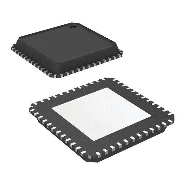
| 产品图片 |
|
| rohs | 符合RoHS无铅 / 符合限制有害物质指令(RoHS)规范要求 |
| 产品系列 | RF集成电路,射频收发器,Analog Devices ADF7025BCPZ- |
| 数据手册 | |
| 产品型号 | ADF7025BCPZ |
| 产品培训模块 | http://www.digikey.cn/PTM/IndividualPTM.page?site=cn&lang=zhs&ptm=12876 |
| 产品目录页面 | |
| 产品种类 | 射频收发器 |
| 传输供电电流 | 19.3 mA |
| 功率-输出 | -20dBm ~ 13dBm |
| 包装 | 托盘 |
| 商标 | Analog Devices |
| 天线连接器 | PCB,表面贴装 |
| 存储容量 | - |
| 安装风格 | SMD/SMT |
| 封装 | Tray |
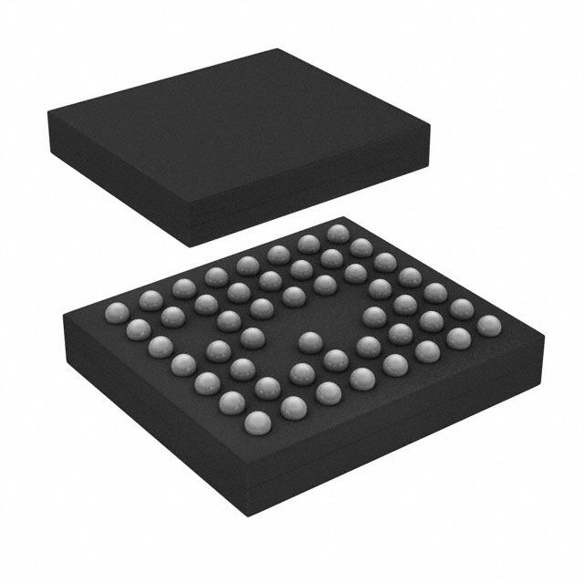
| 封装/外壳 | 48-VFQFN 裸露焊盘,CSP |
| 封装/箱体 | LFCSP-48 EP |
| 工作温度 | -40°C ~ 85°C |
| 工作电源电压 | 2.3 V to 3.6 V |
| 工厂包装数量 | 260 |
| 应用 | 无匙门禁系统,家庭自动化,无线音频/视频 |
| 接口类型 | 3-Wire Serial |
| 接收供电电流 | 19 mA |
| 数据接口 | PCB,表面贴装 |
| 数据速率(最大值) | 384kbps |
| 最大工作温度 | + 85 C |
| 最大数据速率 | 384 kbps |
| 最小工作温度 | - 40 C |
| 标准包装 | 1 |
| 灵敏度 | -104.2 dBm |
| 电压-电源 | 2.3 V ~ 3.6 V |
| 电流-传输 | 28mA |
| 电流-接收 | 19mA |
| 电源电压-最大 | 3.6 V |
| 电源电压-最小 | 2.3 V |
| 类型 | ISM |
| 系列 | ADF7025 |
| 视频文件 | http://www.digikey.cn/classic/video.aspx?PlayerID=1364138032001&width=640&height=505&videoID=2245193150001 |
| 调制或协议 | FSK |
| 调制格式 | ASK, FSK |
| 输出功率 | - 16 dBm to + 13 dBm |
| 配用 | /product-detail/zh/EVAL-ADF70XXEKZ1/EVAL-ADF70XXEKZ1-ND/1530782/product-detail/zh/EVAL-ADF7025DBZ1/EVAL-ADF7025DBZ1-ND/1530781 |
| 频率 | 431MHz ~ 464MHz,862MHz ~ 870MHz 和 902MHz ~ 928MHz |
| 频率范围 | 902 MHz to 928 MHz |

.jpg)


_renders/CS4265-CNZR.jpg)


- 商务部:美国ITC正式对集成电路等产品启动337调查
- 曝三星4nm工艺存在良率问题 高通将骁龙8 Gen1或转产台积电
- 太阳诱电将投资9.5亿元在常州建新厂生产MLCC 预计2023年完工
- 英特尔发布欧洲新工厂建设计划 深化IDM 2.0 战略
- 台积电先进制程称霸业界 有大客户加持明年业绩稳了
- 达到5530亿美元!SIA预计今年全球半导体销售额将创下新高
- 英特尔拟将自动驾驶子公司Mobileye上市 估值或超500亿美元
- 三星加码芯片和SET,合并消费电子和移动部门,撤换高东真等 CEO
- 三星电子宣布重大人事变动 还合并消费电子和移动部门
- 海关总署:前11个月进口集成电路产品价值2.52万亿元 增长14.8%

PDF Datasheet 数据手册内容提取
High Performance ISM Band Transceiver IC Data Sheet ADF7025 FEATURES On-chip VCO and Fractional-N PLL On-chip, 7-bit ADC and temperature sensor Low power, zero-IF RF transceiver Digital RSSI Frequency bands Integrated TRx switch 431 MHz to 464 MHz Leakage current < 1 μA in power-down mode 862 MHz to 870 MHz 902 MHz to 928 MHz APPLICATIONS Data rates supported 9.6 kbps to 384 kbps, FSK Wireless audio/video 2.3 V to 3.6 V power supply Remote control/security systems Programmable output power Wireless metering −16 dBm to +13 dBm in 63 steps Keyless entry Receiver sensitivity Home automation −104.2 dBm at 38.4 kbps, FSK −100 dBm at 172.8 kbps, FSK −95.8 dBm at 384 kbps, FSK Low power consumption 19 mA in receive mode 28 mA in transmit mode (10 dBm output) FUNCTIONAL BLOCK DIAGRAM RSET CREG(1:4) ADCIN MUXOUT RLNA BIAS LDO(1:4) OFFSET TEMP TEST MUX SENSOR CORRECTION LNA RFIN FSK DATA LP FILTER RSSI MUX 7-BIT ADC DEMODULATOR SYNCHRONIZER RFINB GAIN OFFSET CORRECTION CE AGC DATA CLK CONTROL Tx/Rx CONTROL DATA I/O FSK MOD Σ-∆ CONTROL MODULATOR INT/LOCK DIVIDERS/ RFOUT DIV P N/N+1 MUXING SLE SERIAL SDATA PORT SREAD VCO CP PFD SCLK CLK DIV R RING OSC DIV VCOIN CPOUT OSC1 OSC2 CLKOUT 05542-001 Figure 1. Rev. C Document Feedback Information furnished by Analog Devices is believed to be accurate and reliable. However, no responsibility is assumed by Analog Devices for its use, nor for any infringements of patents or other One Technology Way, P.O. Box 9106, Norwood, MA 02062-9106, U.S.A. rights of third parties that may result from its use. Specifications subject to change without notice. No license is granted by implication or otherwise under any patent or patent rights of Analog Devices. Tel: 781.329.4700 ©2006–2016 Analog Devices, Inc. All rights reserved. Trademarks and registered trademarks are the property of their respective owners. Technical Support www.analog.com
ADF7025 Data Sheet TABLE OF CONTENTS Features .............................................................................................. 1 Automatic Sync Word Recognition ......................................... 22 Applications ....................................................................................... 1 Applications Section....................................................................... 23 Functional Block Diagram .............................................................. 1 LNA/PA Matching ...................................................................... 23 Revision History ............................................................................... 2 Transmit Protocol and Coding Considerations ..................... 24 General Description ......................................................................... 3 Device Programming after Initial Power-Up ............................. 24 Specifications ..................................................................................... 4 Interfacing to Microcontroller/DSP ........................................ 24 Timing Characteristics ..................................................................... 7 Serial Interface ................................................................................ 27 Timing Diagrams .......................................................................... 7 Readback Format ........................................................................ 27 Absolute Maximum Ratings ............................................................ 9 Registers ........................................................................................... 28 ESD Caution .................................................................................. 9 Register 0—N Register ............................................................... 28 Pin Configuration and Function Descriptions ........................... 10 Register 1—Oscillator/Filter Register ...................................... 29 Typical Performance Characteristics ........................................... 12 Register 2—Transmit Modulation Register ............................ 30 Frequency Synthesizer ................................................................... 15 Register 3—Receiver Clock Register ....................................... 31 Reference Input Section ............................................................. 15 Register 4—Demodulator Setup Register ............................... 32 Choosing Channels for Best System Performance ................. 17 Register 5—Sync Byte Register ................................................. 33 Transmitter ...................................................................................... 18 Register 6—Correlator/Demodulator Register ...................... 34 RF Output Stage .......................................................................... 18 Register 7—Readback Setup Register ...................................... 35 Modulation Scheme ................................................................... 18 Register 8—Power-Down Test Register .................................. 36 Receiver ............................................................................................ 19 Register 9—AGC Register ......................................................... 37 RF Front End ............................................................................... 19 Register 10—AGC 2 Register .................................................... 38 RSSI/AGC .................................................................................... 20 Register 12—Test Register ......................................................... 39 FSK Demodulators on the ADF7025 ....................................... 20 Register 13—Offset Removal and Signal Gain Register ....... 40 FSK Correlator/Demodulator ................................................... 20 Outline Dimensions ....................................................................... 41 Linear FSK Demodulator .......................................................... 22 Ordering Guide .......................................................................... 41 REVISION HISTORY 9/2016—Rev. B to Rev. C 2/2006—Rev. 0 to Rev. A Changes to General Description Section ...................................... 3 Replaced Figure 40 ................................................................ Page 29 Changes to Interfacing to Microcontroller/DSP Section and Figure 34 ........................................................................................... 24 1/2006—Revision 0: Initial Version 8/2012—Rev. A to Rev. B Changed CP-48-3 Package to CP-48-5 (Throughout) ................. 1 Added EPAD Notation to Figure 6 ............................................... 10 Updated Outline Dimensions ....................................................... 41 Changes to Ordering Guide .......................................................... 41 Rev. C | Page 2 of 41
Data Sheet ADF7025 GENERAL DESCRIPTION The ADF7025 is a low power, highly integrated FSK transceiver. A zero-IF architecture is used in the receiver, minimizing power It is designed for operation in the license–free ISM bands of consumption and the external component count, while avoiding 433 MHz, 863 MHz to 870 MHz, and 902 MHz to 928 MHz. the need for image rejection. The baseband filter (low-pass) has The ADF7025 can be used for applications operating under the programmable bandwidths of ±300 kHz, ±450 kHz, and ±600 kHz. European ETSI EN300-220 or the North American FCC (Part 15) A high-pass pole at ~60 kHz eliminates the problem of dc offsets regulatory standards. The ADF7025 is intended for wideband, that is characteristic of zero-IF architecture. high data rate applications with deviation frequencies from The ADF7025 supports a wide variety of programmable 100 kHz to 750 kHz and data rates from 9.6 kbps to 384 kbps. features, including Rx linearity, sensitivity, and filter bandwidth, A complete transceiver can be built using a small number of allowing the user to trade off receiver sensitivity and selectivity external discrete components, making the ADF7025 very against current consumption, depending on the application. suitable for price-sensitive and area-sensitive applications. An on-chip ADC provides readback of an integrated The transmit section contains a VCO and low noise temperature sensor, an external analog input, the battery Fractional-N PLL with output resolution of <1 ppm. The VCO voltage, or the RSSI signal, which provides savings on an ADC operates at twice the fundamental frequency to reduce spurious in some applications. The temperature sensor is accurate to emissions and frequency pulling problems. ±10°C over the full operating temperature range of −40°C to +85°C. This accuracy can be improved by doing a 1-point The transmitter output power is programmable in 0.3 dB steps calibration at room temperature and storing the result in from −16 dBm to +13 dBm. The transceiver RF frequency and memory. modulation are programmable using a simple 3-wire interface. The device operates with a power supply range of 2.3 V to 3.6 V and can be powered down when not in use. Rev. C | Page 3 of 41
ADF7025 Data Sheet SPECIFICATIONS V = 2.3 V to 3.6 V, GND = 0 V, T = T to T , unless otherwise noted. Typical specifications are at V = 3 V, T = 25°C. DD A MIN MAX DD A All measurements are performed using the EVAL-ADF7025DBZ1 using PN9 data sequence, unless otherwise noted. Table 1. Parameter Min Typ Max Unit Test Conditions RF CHARACTERISTICS Frequency Ranges (Direct Output) 862 870 MHz VCO adjust = 0, VCO bias = 10 902 928 VCO adjust = 3, VCO bias = 12 Frequency Ranges (Divide-by-2 Mode) 431 464 MHz See conditions for direct output Phase Frequency Detector Frequency RF/256 24 MHz TRANSMISSION PARAMETERS Data Rate FSK 9.6 384 kbps FSK Frequency Deviation 100 311.89 kHz PFD = 10 MHz, direct output 100 748.54 kHz PFD = 24 MHz, direct output 100 374.27 kHz PFD =24 MHz, divide-by-2 mode Deviation Frequency Resolution 221 Hz PFD = 3.625 MHz Gaussian Filter BT 0.5 Transmit Power1 −20 +13 dBm VDD = 3.0 V, TA = 25°C Transmit Power Variation vs. Temperature ±1 dB From −40°C to +85°C Transmit Power Variation vs. V ±1 dB From 2.3 V to 3.6 V at 915 MHz, T = 25°C DD A Transmit Power Flatness ±1 dB From 902 MHz to 928 MHz, 3 V, T = 25°C A Programmable Step Size −20 dBm to +13 dBm 0.3125 dB Spurious Emissions Integer Boundary −55 dBc 50 kHz loop B/W Reference −65 dBc Harmonics Second Harmonic −27 dBc Unfiltered conductive Third Harmonic −21 dBc All Other Harmonics −35 dBc VCO Frequency Pulling 30 kHz rms DR = 9.6 kbps Optimum PA Load Impedance 39 + j61 Ω F = 915 MHz RF 48 + j54 Ω F = 868 MHz RF 54 + j94 Ω F = 433 MHz RF RECEIVER PARAMETERS FSK Input Sensitivity At BER = 1E − 3, FRF = 915 MHz, LNA and PA matched separately2 Sensitivity at 38.4 kbps −104.2 dBm F = 200 kHz, LPF B/W = ±300kHz DEV Sensitivity at 172.8 kbps −100 dBm F = 200 kHz, LPF B/W = ±450kHz DEV Sensitivity at 384 kbps −95.8 dBm F = 450kHz, LPF B/W = ±600kHz DEV Baseband Filter (Low-Pass) Bandwidths Programmable ±300 kHz ±450 kHz ±600 kHz LNA and Mixer, Input IP3 Enhanced Linearity Mode +6.8 dBm P = −20 dBm, 2 CW interferers IN Low Current Mode −3.2 dBm F = 915 MHz, f1 = F + 3 MHz RF RF High Sensitivity Mode −35 dBm F2 = F + 6 MHz, maximum gain RF Rx Spurious Emissions3 −57 dBm <1 GHz at antenna input −47 dBm >1 GHz at antenna input Rev. C | Page 4 of 41
Data Sheet ADF7025 Parameter Min Typ Max Unit Test Conditions CHANNEL FILTERING Adjacent Channel Rejection 27 dB Desired signal (38.4 kbps DR, 200 kHz F , DEV (Offset = ±1 × LP Filter BW Setting) ±300 KHz LP filter B/W) 6 dB above the input Second Adjacent Channel Rejection 40 dB sensitivity level, CW interferer power level (Offset = ±2 × LP Filter BW Setting) increased until BER = 10−3 Third Adjacent Channel Rejection 43 dB (Offset = ±3 × LP Filter BW Setting) Co-Channel Rejection −2 +24 dB Maximum rejection measured with CW interferer at center of channel Wideband Interference Rejection 70 dB Swept from 100 MHz to 2 GHz, measured as channel rejection BLOCKING Desired signal (38.4 kbps DR, 200 kHz F , DEV ±1 MHz 42 dB ±300 KHz LP filter B/W) 6 dB above the input sensitivity level, CW interferer power level ±2 MHz 51 dB increased until BER = 10−3 ±10 MHz 64 dB Saturation (Maximum Input Level) 12 dBm FSK mode, BER = 10−3 LNA Input Impedance 24 − j60 Ω FRF = 915 MHz, RFIN to GND 26 − j63 Ω FRF = 868 MHz 71 − j128 Ω FRF = 433 MHz RSSI Range at Input −100 to dBm −36 Linearity ±2 dB Absolute Accuracy ±3 dB Response Time 150 µs PHASE-LOCKED LOOP VCO Gain 65 MHz/V 902 MHz to 928 MHz band, VCO adjust = 3, VCO_BIAS_SETTING = 12 83 MHz/V 862 MHz to 870 MHz band, VCO adjust = 0, VCO_BIAS_SETTING = 10 Phase Noise (In-Band) −89 dBc/Hz PA = 0 dBm, V = 3.0 V, PFD = 10 MHz, DD FRF = 868 MHz, VCO_BIAS_SETTING = 10 Phase Noise (Out-of-Band) −110 dBc/Hz 1 MHz offset Residual FM 128 Hz From 200 Hz to 20 kHz, F = 868MHz RF PLL Settling Time 40 µs Measured for a 10 MHz frequency step to within 5 ppm accuracy, PFD = 20 MHz, LBW = 50kHz REFERENCE INPUT Crystal Reference 3.625 24 MHz External Oscillator 3.625 24 MHz Load Capacitance 33 pF Crystal Start-Up Time 1.0 ms Using 33 pF load capacitors Input Level CMOS levels TIMING INFORMATION Chip Enabled to Regulator Ready 10 µs C = 100 nF REG Crystal Oscillator Startup Time 1 ms With 19.2 MHz XTAL Tx to Rx Turnaround Time 150 µs + Time to synchronized data, includes AGC (5 × T ) settling BIT Rev. C | Page 5 of 41
ADF7025 Data Sheet Parameter Min Typ Max Unit Test Conditions LOGIC INPUTS Input High Voltage, V 0.7 × V V INH DD Input Low Voltage, V 0.2 × V V INL DD Input Current, I /I ±1 µA INH INL Input Capacitance, C 10 pF IN Control Clock Input 50 MHz LOGIC OUTPUTS Output High Voltage, V DV − 0.4 V I = 500 µA OH DD OH Output Low Voltage, V 0.4 V I = 500 µA OL OL CLK Rise/Fall 5 ns OUT CLK Load 10 pF OUT TEMPERATURE RANGE, T −40 +85 °C A POWER SUPPLIES Voltage Supply V 2.3 3.6 V All VDD pins must be tied together DD Transmit Current Consumption FRF = 915 MHz, V = 3.0 V, PA is matched in DD to 50 Ω −20 dBm 14.6 mA −10 dBm 15.8 mA 0 dBm 19.3 mA 10 dBm 28 mA Receive Current Consumption Low Current Mode 19 mA High Sensitivity Mode 21 mA Power-Down Mode Low Power Sleep Mode 0.1 1 µA 1 Measured as maximum unmodulated power. Output power varies with both supply and temperature. 2 Sensitivity for combined matching network case is typically 2 dB less than separate matching networks. 3 Follow the matching and layout guidelines in the LNA/PA Matching section to achieve the relevant FCC/ETSI specifications. Rev. C | Page 6 of 41
Data Sheet ADF7025 TIMING CHARACTERISTICS V = 3 V ± 10%; V = 0 V, T = 25°C, unless otherwise noted. DD GND A Table 2. Parameter1 Limit at T to T Unit Test Conditions/Comments MIN MAX t1 <10 ns SDATA to SCLK setup time t2 <10 ns SDATA to SCLK hold time t3 <25 ns SCLK high duration t4 <25 ns SCLK low duration t5 <10 ns SCLK to SLE setup time t6 <20 ns SLE pulse width t8 <25 ns SCLK to SREAD data valid, readback t9 <25 ns SREAD hold time after SCLK, readback t10 <10 ns SCLK to SLE disable time, readback 1 Guaranteed by design, not production tested. TIMING DIAGRAMS t t 3 4 SCLK t t 1 2 DB1 DB0 (LSB) SDATA DB31 (MSB) DB30 DB2 (CONTROL BIT C2) (CONTROL BIT C1) t 6 SLE t5 05542-002 Figure 2. Serial Interface Timing Diagram t t 1 2 SCLK SDATA REG7 DB0 (CONTROL BIT C1) SLE t 3 t 10 SREAD X RV16 RV15 RV2 RV1 t8 t9 05542-003 Figure 3. Readback Timing Diagram Rev. C | Page 7 of 41
ADF7025 Data Sheet ±1 × DATA RATE/32 1/DATA RATE RxCLK RxDATA DATA 05542-004 Figure 4. RxData/RxCLK Timing Diagram Rev. C | Page 8 of 41
Data Sheet ADF7025 ABSOLUTE MAXIMUM RATINGS T = 25°C, unless otherwise noted. Stresses at or above those listed under Absolute Maximum A Ratings may cause permanent damage to the product. This is a Table 3. stress rating only; functional operation of the product at these Parameter Rating or any other conditions above those indicated in the operational V to GND1 −0.3 V to +5 V section of this specification is not implied. Operation beyond DD Analog I/O Voltage to GND −0.3 V to AV + 0.3 V the maximum operating conditions for extended periods may DD Digital I/O Voltage to GND −0.3 V to DV + 0.3 V affect product reliability. DD Operating Temperature Range This device is a high performance, RF integrated circuit with an Industrial (B Version) −40°C to +85°C ESD rating of <2 kV, and it is ESD sensitive. Proper precautions Storage Temperature Range −65°C to +125°C should be taken for handling and assembly. Maximum Junction Temperature 125°C MLF θ Thermal Impedance 26°C/W ESD CAUTION JA Lead Temperature Soldering Vapor Phase (60 sec) 235°C Infrared (15 sec) 240°C 1 GND = CPGND = RFGND = DGND = AGND = 0 V. Rev. C | Page 9 of 41
ADF7025 Data Sheet PIN CONFIGURATION AND FUNCTION DESCRIPTIONS OCV1DNDNDNG OCDNDDTUOP3GER3DD1CS2CSTUOXU CGGVGVCVVOOM 876543210987 444444444333 VCOIN 1 36CLKOUT VREG1 2 35DATA CLK VDD1 3 34DATA I/O RFOUT 4 33INT/LOCK RFGND 5 ADF7025 32VDD2 RFIN 6 31VREG2 TOP VIEW RFINB 7 (Not to Scale) 30ADCIN RLNA 8 29GND2 VDD4 9 28SCLK RSET 10 27SREAD VREG4 11 26SDATA GND4 12 25SLE 345678901234 111111122222 N1.O CTOENSNECT THE EI_XMIXPI_XIMOSQ_XIMEDQ_XIM P_ITLIFADI_TLIF TO4DNG GQ_TLFINDQ_TLIF. 4DNGA_TSETEC 05542-006 Figure 5. Pin Configuration Table 4. Pin Function Descriptions Pin No. Mnemonic Description 1 VCOIN The tuning voltage on this pin determines the output frequency of the voltage-controlled oscillator (VCO). The higher the tuning voltage, the higher the output frequency. 2 VREG1 Regulator Voltage for PA Block. A 100 nF in parallel with a 5.1 pF capacitor should be placed between this pin and ground for regulator stability and noise rejection. 3 VDD1 Voltage Supply for PA Block. Decoupling capacitors of 0.1 μF and 10 pF should be placed as close as possible to this pin. All VDD pins should be tied together. 4 RFOUT The modulated signal is available at this pin. Output power levels are from −20 dBm to +13 dBm. The output should be impedance-matched to the desired load using suitable components. See the Transmitter section. 5 RFGND Ground for Output Stage of Transmitter. 6 RFIN LNA Input for Receiver Section. Input matching is required between the antenna and the differential LNA input to ensure maximum power transfer. See the LNA/PA Matching section. 7 RFINB Complementary LNA Input. See the LNA/PA Matching section. 8 R External bias resistor for LNA. Optimum resistor is 1.1 kΩ with 5% tolerance. LNA 9 VDD4 Voltage supply for LNA/MIXER Block. This pin should be decoupled to ground with a 10 nF capacitor. 10 RSET External Resistor to Set Charge Pump Current and Some Internal Bias Currents. Use 3.6 kΩ with 5% tolerance. 11 VREG4 Regulator Voltage for LNA/MIXER Block. A 100 nF capacitor should be placed between this pin and GND for regulator stability and noise rejection. 12 GND4 Ground for LNA/MIXER Block. 13 to 18 MIX/FILT Signal Chain Test Pins. These pins are high impedance under normal conditions and should be left unconnected. 19, 22 GND4 Ground for LNA/MIXER Block. 20, 21, 23 FILT/TEST_A Signal Chain Test Pins. These pins are high impedance under normal conditions and should be left unconnected. 24 CE Chip Enable. Bringing CE low puts the ADF7025 into complete power-down. Register values are lost when CE is low, and the part must be reprogrammed once CE is brought high. 25 SLE Load Enable, CMOS Input. When LE goes high, the data stored in the shift registers is loaded into one of the four latches. A latch is selected using the control bits. 26 SDATA Serial Data Input. The serial data is loaded MSB first with the two LSBs as the control bits. This pin is a high impedance CMOS input. 27 SREAD Serial Data Output. This pin is used to feed readback data from the ADF7025 to the microcontroller. The SCLK input is used to clock each readback bit (ADC readback) from the SREAD pin. 28 SCLK Serial Clock Input. This serial clock is used to clock in the serial data to the registers. The data is latched into the 24-bit shift register on the CLK rising edge. This pin is a digital CMOS input. Rev. C | Page 10 of 41
Data Sheet ADF7025 Pin No. Mnemonic Description 29 GND2 Ground for Digital Section. 30 ADCIN Analog-to-Digital Converter Input. The internal 7-bit ADC can be accessed through this pin. Full scale is 0 V to 1.9 V. Readback is made using the SREAD pin. 31 VREG2 Regulator Voltage for Digital Block. A 100 nF in parallel with a 5.1 pF capacitor should be placed between this pin and ground for regulator stability and noise rejection. 32 VDD2 Voltage Supply for Digital Block. A decoupling capacitor of 10 nF should be placed as close as possible to this pin. 33 INT/LOCK Bidirectional Pin. In output mode (interrupt mode), the ADF7025 asserts the INT/LOCK pin when it has found a match for the preamble sequence. In input mode (lock mode), the microcontroller can be used to lock the demodulator threshold when a valid preamble has been detected. Once the threshold is locked, NRZ data can be reliably received. In this mode, a demodulator lock can be asserted with minimum delay. 34 DATA I/O Transmit Data Input/Received Data Output. This is a digital pin, and normal CMOS levels apply. 35 DATA CLK In receive mode, the pin outputs the synchronized data clock. The positive clock edge is matched to the center of the received data. 36 CLKOUT A Divided-Down Version of the Crystal Reference with Output Driver. The digital clock output can be used to drive several other CMOS inputs, such as a microcontroller clock. The output has a 50:50 mark-space ratio. 37 MUXOUT This pin provides the LOCK_DETECT signal, which is used to determine if the PLL is locked to the correct frequency. Other signals include REGULATOR_READY, which is an indicator of the status of the serial interface regulator. 38 OSC2 The reference crystal should be connected between this pin and OSC1. A TCXO reference can be used by driving this pin with CMOS levels and disabling the crystal oscillator. 39 OSC1 The reference crystal should be connected between this pin and OSC2. 40 VDD3 Voltage Supply for the Charge Pump and PLL Dividers. This pin should be decoupled to ground with a 0.01 µF capacitor. 41 VREG3 Regulator Voltage for Charge Pump and PLL Dividers. A 100 nF in parallel with a 5.1 pF capacitor should be placed between this pin and ground for regulator stability and noise rejection. 42 CPOUT Charge Pump Output. This output generates current pulses that are integrated in the loop filter. The integrated current changes the control voltage on the input to the VCO. 43 VDD Voltage Supply for VCO Tank Circuit. This pin should be decoupled to ground with a 0.01 µF capacitor. 44 to 47 GND Grounds for VCO Block. 48 CVCO A 22 nF capacitor should be placed between this pin and VREG1 to reduce VCO noise. EPAD Exposed Pad. Connect the exposed pad to GND. Rev. C | Page 11 of 41
ADF7025 Data Sheet TYPICAL PERFORMANCE CHARACTERISTICS CARRIER POWER 6.11dBm ATTEN 2.00dB MKR1 10.00KHz MKR4 3.482GHz REF –60dBc/Hz 10.00dB/ –88.46dBc/Hz REF 10dBm ATTEN 20dB SWEEP 16.52ms (601pts) PEAK 1 LOG 10dB/ 1 3 4 REF LEVEL 10.00dBm 100Hz FREQUENCY OFFSET 10H05542-007z SRTEASR BTW 1 030MMHHzz VBW 3MHz SWEEP 1S6T.O52Pm 1s0 .(060001GptHsz) 05542-010 Figure 6. Phase Noise Response at 915 MHz, VDD = 3.0 V, ICP = 0.867 mA Figure 9. Harmonic Response, RFOUT Matched to 50 Ω, No Filter REF 10dBm MKR1 400Hz ∆ Mkr1 1.834GHz NORM LOG 10dB/ ATTEN 20dB 0.69dB REF 15dBm ATTEN 30dB –62.57dB 1R NORM 1R 1 LOG 10dB/ MARKER∆ 1.834000000GHz –62.57dB LgAv W1S2 1 S3FC AA £(f): FTun 05542-008 Swp C#REENST EBRW 9 1105k.0H0zMHz VBW 10kHzSWEEP 60.32SmPsA (N60 51MptHsz) S#RTAERS TB 8W0 03M0kHHzz VBW 30kHz SWEEPS 5T.6O2P7 s5 .(060001GptHsz) 05542-011 Figure 7. Output Spectrum in FSK Modulation (915 MHz, Figure 10. Harmonic Response, Murata Dielectric Filter 172.8 kbps Data Rate, 200 kHz Frequency Deviation) 0 20 9µA –5 15 –10 FILT±6E0R0KB/HWz 10 11µA B) EL(d –15 ER 5 V –20 ±450KHz W 5µA LE FILTERB/W PO 0 TION –25 PUT –5 7µA UA –30 UT TTEN –35 ±F3IL0T0EKRHzB/W PA O –10 A –15 –40 ––45–501800–1500–1200–900 –60F0R–E3Q00UEN0CY3(K00Hz)600 900 1200 1500 1800 05542-009 ––2205 1 5 9 13 17 21 25PA2 S9ET3T3IN3G7 41 45 49 53 57 61 05542-053 Figure 8. Baseband Filter Response Figure 11. PA Output Power vs. Setting Rev. C | Page 12 of 41
Data Sheet ADF7025 20 0 DATA RATE = 384k, FDEV = 450k –1 DATA RATE = 172k, FDEV = 200k 0 DATA RATE = 38.4k, FDEV = 200k ACTUAL INPUT LEVEL –2 –20 B) –3 LEVEL (d ––6400 RSSI READBACK LEVEL OG(BER) –4 SI L –5 S R –80 –6 ––1102–00120 –100 –80 –R60F I/P (d–B4)0 –20 0 20 05542-014 –––87116 –108 RF– I1/P00LEVEL(dBm)–90 –7805542-016 Figure 12. Digital RSSI Readback Figure 15. BER vs. Data Rate (Combined Matching Network) 70 –50 = CORRELATOR –55 60 = LINEAR –60 (dB) 50 Bm) –65 N d TIO 40 NT( –70 EC OI OF REJ 2300 TIVITYP ––8705 LEVEL 10 SENSI –85 –90 –100 05542-013 –1–0905 05542-017 –12 –6 0 6 12 0 50 100150200250300350400450500550600650700750800 OFFSETOF INTERFERERFROMWANTEDSIGNAL(MHz) DEVIATIONFREQUENCY (kHz) Figure 13. Wideband Interference Rejection; Wanted Signal (901 MHz, Figure 16. Sensitivity vs. Mod Index (Data Rate = 384 kbps, Baseband Filter 38.4 kbps Data Rate, 200 kHz Frequency Deviation) at 6 dB Above Sensitivity Bandwidth = ±600 kHz), for Both Demodulator Types Point; Interferer = CW Jammer 0 –60 ==CCOORRRREELLAATTOORR –1 –65 ==LLIINNEEAARR –70 –2 m) B d –75 –3 T( BBBW=±450kHz BBBW=±600kHz N ER –4 POI –80 B Y 2.3V,+25°C T –85 –5 33V.6,V+,2+52°5C°C SITIVI –90 2.3V,–40°C N –6 3V,–40°C SE –95 3.6V,–40°C ––87 233V..36,VV+,,8++588°55C°°CC 05542-015 ––110050 05542-018 –115 –110 –105 –100 –95 –90 –85 0 50 100 150 200 250 300 350 400 450 500 550 600 RFI/PLEVEL(dBm) DEVIATIONFREQUENCY(kHz) Figure 14. Sensitivity vs. VDD and Temperature (172.8 kbps Data Rate, Figure 17. Sensitivity vs. Mod Index (Data Rate = 172.8 kbps), for Both 200 kHz Frequency Deviation, Baseband Bandwidth ±600 kHz) Demodulator Types Rev. C | Page 13 of 41
ADF7025 Data Sheet –60 =CORRELATOR –65 =LINEAR –70 m) B –75 d ( NT –80 OI P –85 Y BB BW = BB BW = BB BW = T VI –90 ±300kHz ±450kHz ±600kHz TI SI N –95 E S –100 ––111005 05542-052 0 50 100 150 200 250 300 350 400 450 500 550 600 DEVIATIONFREQUENCY (kHz) Figure 18. Sensitivity vs. Mod Index (Data Rate = 38.4 kbps), for both Demodulator Types Rev. C | Page 14 of 41
Data Sheet ADF7025 FREQUENCY SYNTHESIZER REFERENCE INPUT SECTION R Counter The on-board crystal oscillator circuitry (see Figure 19) can use The 3-bit R counter divides the reference input frequency by an an inexpensive quartz crystal as the PLL reference. The oscillator integer from 1 to 7. The divided-down signal is presented as the circuit is enabled by setting R1_DB12 high. It is enabled by reference clock to the phase frequency detector (PFD). The divide default on power-up and is disabled by bringing CE low. Errors ratio is set in Register 1. Maximizing the PFD frequency reduces in the crystal can be corrected by adjusting the Fractional-N the N value. This reduces the noise multiplied at a rate of 20 log(N) value (see the N Counter section). A single-ended reference to the output, as well as reducing occurrences of spurious (TCXO, CXO) can also be used. The CMOS levels should be components. The R register defaults to R = 1 on power-up. applied to OSC2 with R1_DB12 set low. PFD [Hz] = XTAL/R MUXOUT and Lock Detect The MUXOUT pin allows the user to access various digital points in the ADF7025. The state of MUXOUT is controlled by OSC1 OSC2 Bits R0_DB[29:31]. CP2 CP1 05542-019 Regulator Ready Figure 19. Oscillator Circuit on the ADF7025 Regulator ready is the default setting on MUXOUT after the Two parallel resonant capacitors are required for oscillation at transceiver has been powered up. The power-up time of the the correct frequency; their values are dependent on the crystal regulator is typically 50 μs. Because the serial interface is powered specification. They should be chosen so that the series value of from the regulator, the regulator must be at its nominal voltage capacitance added to the PCB track capacitance adds up to the before the ADF7025 can be programmed. The status of the load capacitance of the crystal, usually 20 pF. Track capacitance regulator can be monitored at MUXOUT. When the regulator values vary from 2 pF to 5 pF, depending on board layout. ready signal on MUXOUT is high, programming of the Where possible, choose capacitors that have a very low ADF7025 can begin. temperature coefficient to ensure stable frequency operation DVDD over all conditions. CLKOUT Divider and Buffer REGULATOR READY The CLKOUT circuit takes the reference clock signal from DIGITAL LOCK DETECT the oscillator section, shown in Figure 20, and supplies a ANALOG LOCK DETECT divided-down 50:50 mark-space signal to the CLKOUT pin. MUX CONTROL MUXOUT R COUNTER OUTPUT An even divide from 2 to 30 is available. This divide number N COUNTER OUTPUT is set in R1_DB[8:11]. On power-up, the CLKOUT defaults to PLL TEST MODES divide-by-8. Σ-∆ TEST MODES DVDD CENLKAOBLUET BIT DGND 05542-021 Figure 21. MUXOUT Circuit OSC1 DIVIDER ÷2 CLKOUT 1TO 15 05542-020 Digital Lock Detect Digital lock detect is active high. The lock detect circuit is Figure 20. CLKOUT Stage located at the PFD. When the phase error on five consecutive To disable CLKOUT, set the divide number to 0. The output cycles is less than 15 ns, lock detect is set high. Lock detect buffer can drive up to a 20 pF load with a 10% rise time at remains high until a 25 ns phase error is detected at the PFD. 4.8 MHz. Faster edges can result in some spurious feedthrough Because no external components are needed for digital lock to the output. A small series resistor (50 Ω) can be used to slow detect, it is more widely used than analog lock detect. the clock edges to reduce these spurs at F . CLK Rev. C | Page 15 of 41
ADF7025 Data Sheet Analog Lock Detect The fractional divide value gives very fine resolution at the output, where the output frequency of the PLL is calculated as This N-channel open-drain lock detect should be operated with an external pull-up resistor of 10 kΩ nominal. When a lock has XTAL FractionalN F (Integer N ) been detected, this output is high with narrow low-going pulses. OUT R 215 Voltage Regulators REFERENCE IN 4R PFD/ CHARGE VCO The ADF7025 contains four regulators to supply stable voltages PUMP to the part. The nominal regulator voltage is 2.3 V. Each regulator should have a 100 nF capacitor connected between VREG and 4N GND. When CE is high, the regulators and other associated circuitry are powered on, drawing a total supply current of 2 mA. THIRD-ORDER Bringing the chip-enable pin low disables the regulators, Σ-∆ MODULATOR rveadluuecse sh ethlde isnu pthpely r ecguirsrteenrst. tToh lees sse trhiaaln i n1t μerAfa, caen odp eerraasteess aflrlo m FRACTIONAL-N INTEGER-N 05542-023 Figure 23. Fractional-N PLL a regulator supply; therefore, to write to the part, the user must have CE high and the regulator voltage must be stabilized. The combination of the Integer-N (maximum = 255) and the Regulator status (VREG4) can be monitored using the regulator Fractional-N (maximum = 16383/16384) gives a maximum N ready signal from MUXOUT. divider of 255 + 1. Therefore, the minimum usable PFD is Loop Filter PDF [Hz] = Maximum Required Output Frequency/(255 + 1) MIN The loop filter integrates the current pulses from the charge For example, when operating in the European 868 MHz to pump to form a voltage that tunes the output of the VCO to the 870 MHz band, PFD equals 3.4 MHz. MIN desired frequency. It also attenuates spurious levels generated by the PLL. A typical loop filter design is shown in Figure 22. Voltage Controlled Oscillator To minimize spurious emissions, the on-chip VCO operates from 1732 MHz to 1856 MHz. The VCO signal is then divided CHARGE VCO PUMP OUT by 2 to give the required frequency for the transmitter and the 05542-022 rTehqeu VireCdO L sOh ofruelqdu been rcey- fcoern ttehree rde, cdeeivpeern. d ing on the required Figure 22. Typical Loop Filter Configuration frequency of operation, by programming the VCO adjust bits In general, a loop filter bandwidth (LBW) of between the data R1_DB[20:21]. rate and twice the data rate is recommended. Widening the For operation in the 862 MHz to 870 MHz band, it is recom- LBW excessively reduces the time spent jumping between mended to use a VCO bias of at least Setting 10 and to set the frequencies, but it can cause insufficient spurious attenuation. VCO adjust bit to Setting 0. For operation in the 902 MHz to Narrow-loop bandwidths can result in the loop taking long 928 MHz band, it is recommended to use a VCO bias of at least periods of time to attain lock. For the ADF7025 in receive mode, Setting 12 and to set the VCO adjust bit to Setting 3. This is to the loop filter bandwidth affects the close-in blocking perform- ensure correct operation under all conditions. ance. The narrower the bandwidth of the loop filter, the greater the close-in interference resilience of the receiver. The VCO is enabled as part of the PLL by the PLL-enable bit, R0_DB28. Careful design of the loop filter is critical to obtaining accurate FSK modulation. The free design tool ADIsimPLL can be used An additional frequency divide-by-2 is included to allow operation to design loop filters for the ADF7025. in the lower 431 MHz to 464 MHz bands. To enable operation N Counter in these bands, R1_DB13 should be set to 1. The VCO needs an external 22 nF between the VCO and the regulator to reduce The feedback divider in the ADF7025 PLL consists of an 8-bit internal noise. integer counter and a 14-bit Σ-Δ Fractional-N divider. The integer counter is the standard pulse-swallow type common in PLLs. This sets the minimum integer divide value to 31. Rev. C | Page 16 of 41
Data Sheet ADF7025 VCO Bias Current CHOOSING CHANNELS FOR BEST SYSTEM PERFORMANCE VCO bias current can be adjusted using Bit R1_DB19 to Bit R1_DB16. To ensure VCO oscillation under all conditions, The Fractional-N PLL allows the selection of any channel the minimum bias current setting is Setting 12 (0xC). within 862 MHz to 928 MHz (and 431 MHz to 464 MHz using divide-by-2) to a resolution of <300 Hz. This also facilitates 431 MHz to 464 MHz Operation frequency-hopping systems. For operation in the 431 MHz to 464 MHz band, the frequency Careful selection of the RF transmit channels must be made divide-by-2 has to be enabled. It is enabled by R1_DB13. Because to achieve best spurious performance. The architecture of this divide is external to the synthesizer loop, the feedback divider fractional-N results in some level of the nearest integer channel number (N + F) should be programmed to a value twice the moving through the loop to the RF output. These beat-note desired RF output frequency. spurs are not attenuated by the loop, if the desired RF channel and the nearest integer channel are separated by a frequency of VCO BIAS R1_DB (16:19) less than the LBW. TOPAAND N DIVIDER The occurrence of beat-note spurs is rare, because the integer LOOP FILTER VCO ÷2 MUX ÷2 frequencies are at multiples of the reference, which is typically 220µF >10 MHz. CVCO PIN VCO SELECT BIT 05542-024 Baveoaitd-innogt ev esrpyu srms aclaln o rb ve esriyg nlairfgicea vnatlluye rse idnu tcheed f rianc atimonpalli truedgeis tbeyr, using the frequency doubler. By having a channel 1 MHz away Figure 24. Voltage Controlled Oscillator from an integer frequency, a 100 kHz loop filter can reduce the level to less than −45 dBc. Rev. C | Page 17 of 41
ADF7025 Data Sheet TRANSMITTER RF OUTPUT STAGE MODULATION SCHEME The PA of the ADF7025 is based on a single-ended, controlled Frequency Shift Keying (FSK) current, open-drain amplifier that has been designed to deliver Frequency shift keying is implemented by setting the N value for up to 13 dBm into a 50 Ω load at a maximum frequency of the center frequency and then toggling this with the TxData 928 MHz. line. The deviation from the center frequency is set using Bits R2_DB[15:23]. The deviation from the center frequency The PA output current and, consequently, the output power are in Hz is programmable over a wide range. The PA configuration is shown in Figure 25. The output power is independent of the PFD ModulationNumber FSK [Hz] state of the DATA I/O pin. The output power is set using Bits DEVIATION 214 R2_DB[9:14]. where Modulation Number is a number from 1 to 511 R2_DB(30:31) (R2_DB(15:23)). 2 Select FSK using Bits R2_DB[6:8]. 6 IDAC R2_DB(9:14) RFOUT R2_DB4 + R2_DB5 4R PFD/ PA STAGE DIGITAL CHARGE VCO RFGND LOCK DETECT PUMP FROM VCO 05542-025 FSFKR EDQEUVEIANTCIOYN Figure 25. PA Configuration ÷N The PA is equipped with overvoltage protection, which makes –FDEV THIRD-ORDER it robust in severe mismatch conditions. Depending on the +FDEV Σ-∆ MODULATOR aepxhpilbiciat toiopnti,m ounme c eafnf idcieesnigcny aat m thaet cdheisnigre nde rtawdoirakte fdo ro uthtpe uPtA p toow er TxDATA FRACTIONAL-N INTEGER-N 05542-026 Figure 26. FSK Implementation level for a wide range of different antennas, such as loop or monopole antennas. See the LNA/PA Matching section for Modulation Index details. The choice of deviation frequency for a given data rate is critical to get optimum sensitivity performance from the ADF7025. PA Bias Currents The modulation index (MI) of an FSK modulated signal is Control Bits R2_DB [30:31] facilitate an adjustment of the PA defined as bias current to further extend the output power control range, if 2Frequency Deviation[Hz] necessary. If this feature is not required, the default value of MI 7 μA is recommended. The output stage is powered down by DataRate[bps] resetting Bit R2_DB4. It is recommended to use a MI > 1 for the ADF7025. The variation of receiver sensitivity with modulation index, for various data rates, can be observed in Figure 16, Figure 17, and Figure 18. Rev. C | Page 18 of 41
Data Sheet ADF7025 RECEIVER RF FRONT END Based on the specific sensitivity and linearity requirements of the application, it is recommended to adjust control bits The ADF7025 is based on a fully integrated, zero-IF receiver LNA_MODE (R6_DB15) and MIXER_LINEARITY (R6_DB18). architecture. The zero-IF architecture minimizes power consumption and the external component count while avoiding The gain of the LNA is configured by the LNA_GAIN field, the need for image rejection. R9_DB[20:21] and can be set by either the user or the automatic gain control (AGC) logic. Figure 27 shows the structure of the receiver front end. The numerous programming options allow users to trade off Filter Settings/Calibration sensitivity, linearity, and current consumption against each Out-of-band interference is rejected by means of a fifth-order, low- other in the way best suitable for their applications. To achieve pass filter (LPF). The bandwidth of the filter can be programmed to a high level of resilience against spurious reception, the LNA be ±300 kHz, ±450 kHz, or ±600 kHz by means of Control Bits features a differential input. Switch SW2 shorts the LNA input R1_DB[22:23] and should be chosen as a compromise between when transmit mode is selected (R0_DB27 = 0). This feature interference rejection and attenuation of the desired signal. A facilitates the design of a combined LNA/PA matching network, high-pass filter is also included as part of the low-pass filter to avoiding the need for an external Rx/Tx switch. See the prevent against dc offset problems. The bandwidth of this filter LNA/PA Matching section for details on the design of the is ~60 kHz. To avoid significant loss of FSK modulated signal in matching network. the filter, the frequency deviation needs to be significantly I (TO FILTER) larger than this pole (refer to the Modulation Index section). RFIN The minimum allowable frequency deviation is 100 kHz. Tx/Rx SELECT SW2 LNA LO [R0_DB27] RFINB To compensate for manufacturing tolerances, the LPF should Q (TO FILTER) be calibrated once after power-up. The LPF calibration logic LNA MODE [R6_DB15] requires that the LPF divider in Bits R6_DB[20:28] be set MIXER LINEARITY LNA CURRENT [R6_DB18] depending on the crystal frequency. Once initiated by setting [R6_DB(16:17)] Bit R6_DB19, the calibration is performed automatically LNA GAIN without any user intervention. The calibration time is 200 μs, [R9_DB(20:21)] LNA/MIXER[ RE8N_ADBBL6E] 05542-027 dimurpionrgt awnht incoht t thoe iAniDtiFat7e0 t2h5e schaoliublrda tnioont bcey calcec besesfeodre. Itth ies crystal Figure 27. ADF7025 RF Front End oscillator has fully settled. If the AGC loop is disabled, the gain of LPF can be set to three levels using the FILTER_GAIN field, The LNA is followed by a quadrature downconversion mixer, R9_DB[20:21]. The filter gain is adjusted automatically, if the which converts the RF signal direct to baseband. The output AGC loop is enabled. frequency of the synthesizer must be programmed to the value equal to the center frequency of the received channel. The LNA has two basic operating modes: high gain/low noise mode and low gain/low power mode. To switch between the two modes, use the LNA_MODE bit, R6_DB15. The mixer is also configurable between a low current and an enhanced linearity mode using the MIXER_LINEARITY bit, R6_DB18. Rev. C | Page 19 of 41
ADF7025 Data Sheet RSSI/AGC RSSI Formula (Converting to dBm) INPUT_POWER [dBm] = The RSSI is implemented as a successive compression log amp −98 dBm + (READBACK_CODE + following the baseband channel filtering. The log amp achieves GAIN_MODE_CORRECTION) × 0.5 ±3 dB log linearity. It also doubles as a limiter to convert the signal- to-digital levels for the FSK demodulator. Offset correction is where: achieved using a switched capacitor integrator in feedback READBACK_CODE is given by Bit RV7 to Bit RV1 in the around the log amp. This uses the BB offset clock divide. The readback register (see the Readback Format section). RSSI level is converted for user readback and digitally controlled GAIN_MODE_CORRECTION is given by the values in Table 5. AGC by an 80-level (7-bit) flash ADC. This level can be converted to input power in dBm. LNA gain and filter gain (LG2/LG1, FG2/FG1) are also obtained from the readback register. OFFSET CORRECTION Table 5. Gain Mode Correction FSK 1 A A A LATCH DEMOD Gain Mode LNA Gain (LG2, LG1) Filter Gain (FG2, FG1) Correction IFWR IFWR IFWR IFWR CLK H (11) H (10) 0 RSSI M (10) H (10) 17 DEMOD R ADC 05542-028 MM ((1100)) LM ( 0(001) ) 5635 Figure 28. RSSI Block Diagram L (01) L (00) 90 EL (00) L (00) 113 Offset Correction Clock These numbers are for an unmodulated tone. For a modulated In Register 3, the user should set the BB offset clock divide bits signal, the RSSI readback may have to be adjusted to get the R3_DB[4:5] to give an offset clock between 1 MHz and 2 MHz, required accuracy. An additional factor should also be where BBOS _CLK [Hz] = XTAL/(BBOS_CLK_DIVIDE). introduced to account for losses in the front-end matching BBOS_CLK_DIVIDE can be set to 4, 8, or 16. network/antenna. AGC Information FSK DEMODULATORS ON THE ADF7025 In Register 9, the user should select automatic gain control by The two FSK demodulators on the ADF7025 are selecting Auto In R9_DB18 and Auto In R9_DB19. The user FSK correlator/demodulator should then program AGC Low Threshold R9_DB[4:10] and AGC High Threshold R9_DB[11:17]. The default values for the Linear demodulator low and high thresholds are 30 and 70, respectively; however, Select these using the Demod Select Bits R4_DB[4:5]. these are not the optimum settings for all operating conditions. The recommended values for the low and high thresholds are FSK CORRELATOR/DEMODULATOR 15 and 79, respectively. In the AGC 2 register (Register 10), the The quadrature outputs of the IF filter are first limited and then user should program the AGC delay to be long enough to allow fed to a pair of digital frequency correlators that perform band- the loop to settle. The default/recommended value is 10. pass filtering of the binary FSK frequencies at (IF + F ) and DEV AGC_WAIT_TIME (IF − FDEV). Data is recovered by comparing the output levels AGC_DELAYSEQ_CLK_DIVIDE from each of the two correlators. The performance of this frequency discriminator approximates that of a matched filter XTAL detector, which is known to provide optimum detection in the AGC Settling = AGC_WAIT_TIME × Number of Gain presence of AWGN. Changes FREQUENCYCORRELATOR SLICER Tftihvheeun gs ,Aa iinGn Ctchh esa ewnttgoleirnss,tg A c=aG s1eC0, id×f e t5hla eμy sA = ×G 1 C50 ,=l oa 2no5dp0 hS μEassQ. tM_oC ginLoi Kmth =uro m2u0 g0h kaHll z, LIIMITERS 0 OSTD FILTER + ATARONIZER Rx DATA AGC_WAIT_TIME must be at least 25 μs. Q – FDEV + FDEV PDEMO – DSYNCH Rx CLK DB(4:13) DB(14) 0 DB(8:15) 05542-029 Figure 29. FSK Correlator/Demodulator Block Diagram Rev. C | Page 20 of 41
Data Sheet ADF7025 Postdemodulator Filter The discriminator BW is controlled in Register 6 by A second-order, digital low-pass filter removes excess noise R6_DB[4:13] and is defined as from the demodulated bit stream at the output of the DISCRIMINATOR_BW = DEMOD_CLK/(4 × F ) DEV discriminator. The bandwidth of this postdemodulator filter is programmable and must be optimized for the user’s data rate. If where: the bandwidth is set too narrow, performance is degraded due DEMOD_CLK is as defined in the Register 3—Receiver Clock to intersymbol interference (ISI). If the bandwidth is set too Register section. wide, excess noise degrades the receiver’s performance. F is the deviation from the carrier frequency in FSK DEV Typically, the 3 dB bandwidth of this filter is set at approximately modulation. 0.75 times the user’s data rate, using Bits R4_DB[6:15]. Postdemodulator Bandwidth Register Settings Bit Slicer The 3 dB bandwidth of the postdemodulator filter is controlled The received data is recovered by the threshold detecting the by Bits R4_DB[6:15] and is given by output of the postdemodulator low-pass filter. In the correlator/ 210×2π×F demodulator, the binary output signal levels of the frequency POST_DEMOD_BW_SETTING= CUTOFF discriminator are always centered on 0. Therefore, the slicer DEMOD_CLK threshold level can be fixed at 0, and the demodulator where F is the target 3 dB bandwidth in Hz of the post- CUTOFF performance is independent of the run-length constraints of the demodulator filter. This should typically be set to 0.75 times transmit data bit stream. This results in robust data recovery, the data rate (DR). which does not suffer from the classic baseline wander problems that exist in more traditional FSK demodulators. Some sample settings for the FSK correlator/demodulator are Data Synchronizer DEMOD_CLK = 11.0592 MHz An oversampled digital PLL is used to resynchronize the received DR = 200 kbps bit stream to a local clock. The oversampled clock rate of the FDEV = 300 kHz PLL (CDR_CLK) must be set at 32 times the data rate. See the Therefore, Register 3—Receiver Clock Register section for a definition of how to program. The clock recovery PLL can accommodate F = 0.75 × 200 × 103 Hz CUTOFF frequency errors of up to ±2%. POST_DEMOD_BW = 211 × π × 150 × 103 Hz/(11.0592 MHz) FSK Correlator Register Settings POST_DEMOD_BW = Round (87.266) = 87 To enable the FSK correlator/demodulator, Bits R4_DB[5:4] and should be set to 01. To achieve best performance, the bandwidth DISCRIMINATOR_BW = (11.0592 MHz )/(4 × 300 × 103) = of the FSK correlator must be optimized for the specific deviation 9.21 = 9 (rounded to the nearest integer) frequency that is used by the FSK transmitter. Table 6. Register Settings Setting Name Register Address Value POST_DEMOD_BW R4_DB[6:15] 0x09 DISCRIMINATOR_BW R6_DB[4:13] 0x58 Rev. C | Page 21 of 41
ADF7025 Data Sheet LINEAR FSK DEMODULATOR AUTOMATIC SYNC WORD RECOGNITION A block diagram of the linear FSK demodulator is shown in The ADF7025 also supports automatic detection of the sync or Figure 30. ID fields. To activate this mode, the sync (or ID) word must be MUX 1 SLICER preprogrammed into the ADF7025. In receive mode, this ADC RSSI OUTPUT 7 preprogrammed word is compared to the received bit stream + and, when a valid match is identified, the external pin LEVEL Rx DATA I G INT/LOCK is asserted by the ADF7025. GINER LQIMITER FREQ AVERAFILT ELOPEECTOR – Tchhains nfeeal thuarse bcaenen b de eutseecdte tdo. Iatl erretl atxhees m thiec rcoopmropcuetsastoior nthaal tr eaq vuailried- VT 0Hz ENDE ments of the microprocessor and reduces the overall power LINEAR DISCRIMINATOR DB(6:15) 05542-030 caoganisnu maftpetri onnin. Te hdea tIaN cTlo/cLkO cCyKcl eiss. a utomatically de-asserted Figure 30. Block Diagram of Linear FSK Demodulator The automatic sync/ID word detection feature is enabled by This method of frequency demodulation is useful when very selecting Demod Mode 2 or Demod Mode 3 in the demodulator short preamble length is required. setup register. Do this by setting R4_DB[25:23] = [010] or R4_DB[25:23] = [011]. Bits R5_DB[4:5] are used to set the A digital frequency discriminator provides an output signal that length of the sync/ID word, which can be either 12 bits, 16 bits, is linearly proportional to the frequency of the limiter outputs. 20 bits, or 24 bits long. The transmitter must transmit the MSB The discriminator output is then filtered and averaged using a of the sync byte first and the LSB last to ensure proper combined averaging filter and envelope detector. The demodu- alignment in the receiver sync byte detection hardware. lated FSK data is recovered by threshold-detecting the output of the averaging filter, as shown in Figure 30. In this mode, the For systems using FEC, an error tolerance parameter can also slicer output shown in Figure 30 is routed to the data synchro- be programmed that accepts a valid match when up to three bits nizer PLL for clock synchronization. To enable the linear FSK of the word are incorrect. The error tolerance value is assigned demodulator, Bits R4_DB[4:5] are set to [00]. in R5_DB[6:7]. The 3 dB bandwidth of the postdemodulation filter is set in the same way as the FSK correlator/demodulator, which is set in R4_DB[6:15] and is defined as 210 2F POST_DEMOD_BW_SETTING CUTOFF DEMOD_CLK where: F is the target 3 dB bandwidth in Hz of the CUTOFF postdemodulator filter. DEMOD_CLK is as defined in the Register 3—Receiver Clock Register section. Rev. C | Page 22 of 41
Data Sheet ADF7025 APPLICATIONS SECTION LNA/PA MATCHING A first-order implementation of the matching network can be obtained by understanding the arrangement as two L-type The ADF7025 exhibits optimum performance in terms of matching networks in a back-to-back configuration. Due to the sensitivity, transmit power, and current consumption only if its asymmetry of the network with respect to ground, a compro- RF input and output ports are properly matched to the antenna mise between the input reflection coefficient and the maximum impedance. For cost-sensitive applications, the ADF7025 is differential signal swing at the LNA input must be established. equipped with an internal Rx/Tx switch, which facilitates the The use of appropriate CAD software is strongly recommended use of a simple combined passive PA/LNA matching network. for this optimization. Alternatively, an external Rx/Tx switch, such as the Analog Devices ADG919, can be used, which yields a slightly improved Depending on the antenna configuration, the user might need a receiver sensitivity and lower transmitter power consumption. harmonic filter at the PA output to satisfy the spurious emission External Rx/Tx Switch requirement of the applicable government regulations. The harmonic filter can be implemented in various ways, such as a Figure 31 shows a configuration using an external Rx/Tx switch. discrete LC filter or T-stage filter. Dielectric low-pass filter This configuration allows an independent optimization of the components such as the LFL18924MTC1A052 (for operation in matching and filter network in the transmit and receive path, the 915 MHz band), or LFL18869MTC2A160 (for operation in and is, therefore, more flexible and less difficult to design than the 868 MHz band), both by Murata Mfg. Co., Ltd., represent an the configuration using the internal Rx/Tx switch. The PA is attractive alternative to discrete designs. The immunity of the biased through Inductor L1, while C1 blocks dc current. Both ADF7025 to strong out-of-band interference can be improved elements, L1 and C1, also form the matching network, which by adding a band-pass filter in the Rx path. transforms the source impedance into the optimum PA load impedance, ZOPT_PA. Internal Rx/Tx Switch VBAT Figure 32 shows the ADF7025 in a configuration where the internal Rx/Tx switch is used with a combined LNA/PA L1 PA_OUT matching network. This is the configuration used in the EVAL- OPTIONAL PA LPF ADF7025DBZ1. For most applications, the slight performance ANTENNA ZOPT_PA degradation of 1 dB to 2 dB caused by the internal Rx/Tx switch ZIN_RFIN is acceptable, allowing the user to take advantage of the cost- OPTIONAL CA RFIN saving potential of this solution. The design of the combined BPF (SAW) matching network must compensate for the reactance presented LA LNA RFINB by the networks in the Tx and the Rx paths, taking the state of the Rx/Tx switch into consideration. ADG919 ZIN_RFIN Rx/Tx – SELECT CB ADF7025 05542-031 VBAT Figure 31. ADF7025 with External Rx/Tx Switch C1 L1 PA_OUT PA Z _PA depends on various factors such as the required output OPT power, the frequency range, the supply voltage range, and the ANTENNA OPTIONAL ZOPT_PA temperature range. Selecting an appropriate Z _PA helps to BPF OR LPF ZIN_RFIN OPT CA RFIN minimize the Tx current consumption in the application. This data sheet contains a number of ZOPT_PA values for representative LA LNA RFINB conditions. Under certain conditions, however, it is recommended to obtain a suitable Z _PA value by means of a load-pull OPT ZIN_RFIN mDueaes tuor ethmee dnitf.f e rential LNA input, the LNA matching network CB ADF7025 05542-032 Figure 32. ADF7025 with Internal Rx/Tx Switch must be designed to provide both a single-ended to differential conversion and a complex conjugate impedance match. The network with the lowest component count that can satisfy these requirements is the configuration shown in Figure 31, which consists of two capacitors and one inductor. Rev. C | Page 23 of 41
ADF7025 Data Sheet The procedure typically requires several iterations until an Table 7. Minimum Register Writes Required for Tx/Rx Setup acceptable compromise is reached. The successful implementation Mode Registers of a combined LNA/PA matching network for the ADF7025 is critically dependent on the availability of an accurate electrical Tx 0 1 2 model for the PC board. In this context, the use of a suitable CAD Rx (FSK) 0 1 2 4 6 91 package is strongly recommended. To avoid this effort, however, a Tx to Rx and Rx to Tx 0 small form-factor reference design for the ADF7025 is provided, 1 Register 9 should be programmed in receive mode in order to set the including matching and harmonic filter components. The design recommended AGC threshold settings (low = 15, high = 79). is on a 2-layer PCB to minimize cost. Gerber files are available Figure 36 and Figure 37 show the recommended programming on product page at www.analog.com/ADF7025. sequence and associated timing for power-up from standby mode. TRANSMIT PROTOCOL AND CODING CONSIDERATIONS INTERFACING TO MICROCONTROLLER/DSP Low level device drivers are available for interfacing to the PREAMBLE WSYONRCD FIEIDLD DATA FIELD CRC 05542-033 AorD thFe7 0B2l5ac, kthfien A® AnaDloSgP -DBeFv5i3ce3s D, ISnPc .u, AsinDgu tCh8e4 h1a mrdiwcraorec ontroller Figure 33. Typical Format of a Transmit Protocol connections shown in Figure 34 and Figure 35. A dc-free preamble pattern is recommended for FSK demodulation. ADuC841 ADF7025 The recommended preamble pattern is a dc-free pattern such as a 10101010… pattern. Preamble patterns with longer run-length MISO TxRxDATA MOSI constraints such as 11001100…. can also be used. However, this SCLOCK RxCLK results in a longer synchronization time of the received bit SS stream in the receiver. P3.7 CE P3.2/INT0 INT/LOCK Manchester coding can be used for the entire transmit protocol. P2.4 SREAD P2.5 SLE Hdoo nwoetv hear,v teh teo ruesme adicn-ifnrege fcioelddisn gth. Fato fro tlhloeswe tfiheeld psr, ethame AblDe Fh7e0a2d5e r GPIO PP22..67 SSDCLAKTA 05542-034 can accommodate coding schemes with a run-length of up to Figure 34. ADuC841 to ADF7025 Connection Diagram six bits without any performance degradation. ADSP-BF533 ADF7025 If longer run-length coding must be supported, the ADF7025 SCK SCLK MOSI SDATA has several other features that can be activated. These involve a MISO SREAD range of programmable options that allow the envelope detector PF5 SLE output to be frozen after preamble acquisition. RSCLK1 TxRxCLK DT1PRI TxRxDATA DEVICE PROGRAMMING AFTER INITIAL POWER-UP DR1PRI RFS1 INT/LOCK Table 7 lists the minimum number of writes needed to set up PF6 CE tAhded AitDioFn7a0l 2re5g iins teeirtsh cear nT axl soor bRex wmroitdteen a tfote tra CiloEr i sth ber opuargth tto h aig h. GVCNCD VGCNCD 05542-035 Figure 35. ADSP-BF533 to ADF7025 Connection Diagram particular application, such as setting up sync byte detection. When going from Tx to Rx or vice versa, the user needs to write only to the N register to alter the LO by 200 kHz and to toggle the Tx/Rx bit. Rev. C | Page 24 of 41
Data Sheet ADF7025 D D I 5 2 0 7 F D A 19mATO 22mA 14mA XTAL T0 3.65mA 2.0mA RREEAGD.Y WR0 WR1 VCO WR3WR4 WR6 ARGSSCI/ CDR RxDATA TIME T1 T2 T3 T4 T5 T6 T7 T8 T9 T11 TON TOFF 05542-036 Figure 36. Rx Programming Sequence and Timing Diagram Table 8. Power-Up Sequence Description Signal to Parameter Value Description/Notes Monitor T 2 ms XTAL starts power-up after CE is brought high. This typically depends on the XTAL CLKOUT 0 type and the load capacitance specified. T 10 μs Time for regulator to power up. The serial interface can be written to after this time. MUXOUT 1 T, T, T, 32 × 1/SPI_CLK Time to write to a single register. Maximum SPI_CLK is 25 MHz. 2 3 5 T, T 6 7 T 1 ms The VCO can power-up in parallel with the XTAL. This depends on the CVCO CVCO pin 4 capacitance value used. A value of 22 nF is recommended as a trade-off between phase noise performance and power-up time. T 150 μs This depends on the number of gain changes the AGC loop needs to cycle through Analog RSSI 8 and AGC settings programmed. This is described in more detail in the AGC Information on TEST_A pin section. T 5 × BIT_PERIOD This is the time for the clock and data recovery circuit to settle. This typically requires 9 5-bit transitions to acquire sync and is usually covered by the preamble. T Packet length Number of bits in payload by the bit period. 11 Rev. C | Page 25 of 41
ADF7025 Data Sheet D D I 5 2 0 7 F D A 15mATO 30mA 14mA 3.65mA 2.0mA REG. READYWR0WR1 XTAL + VCO WR2 TxDATA TIME T1 T2 T3 T4 T5 T12 TON TOFF 05542-037 Figure 37. Tx Programming Sequence and Timing Diagram Rev. C | Page 26 of 41
Data Sheet ADF7025 SERIAL INTERFACE The serial interface allows the user to program the eleven 32-bit Battery Voltage ADCIN/Temperature Sensor Readback registers using a 3-wire interface (SCLK, SDATA, and SLE). It The battery voltage is measured at Pin VDD4. The readback consists of a level shifter, a 32-bit shift register, and 11 latches. information is contained in Bit RV1 to Bit RV7. This also Signals should be CMOS-compatible. The serial interface is applies for the readback of the voltage at the ADCIN pin and powered by the regulator, and, therefore, is inactive when CE the temperature sensor. From the readback information, the is low. battery or ADCIN voltage can be determined using Data is clocked into the register, MSB first, on the rising edge of V = (BATTERY_VOLTAGE_READBACK)/21.1 BATTERY each clock (SCLK). Data is transferred to one of 11 latches on V = (ADCIN_VOLTAGE_READBACK)/42.1 ADCIN the rising edge of SLE. The destination latch is determined by Silicon Revision Readback the value of the four control bits (C4 to C1). These are the bottom four LSBs, DB3 to DB0, as shown in the timing diagram The silicon revision readback word is valid without setting any in Figure 2. Data can also be read back on the SREAD pin. other registers, especially directly after power-up. The silicon revision word is coded with four quartets in BCD format. The READBACK FORMAT product code (PC) is coded with two quartets extending from The readback operation is initiated by writing a valid control Bit RV9 to Bit RV16. The revision code (RV) is coded with one word to the readback register and setting the readback-enable quartet extending from Bit RV1 to Bit RV8. The product code bit (R7_DB8 = 1). The readback can begin after the control should read back as PC = 0x25. The current revision code word has been latched with the SLE signal. SLE must be kept should read as RC = 0x08. high while the data is being read out. Each active edge at the Filter Calibration Readback SCLK pin clocks the readback word out successively at the SREAD pin, as shown in Figure 38, starting with the MSB first. The filter calibration readback word is contained in Bit RV1 to The data appearing at the first clock cycle following the latch Bit RV8 and is for diagnostic purposes only. Using the automatic operation must be ignored. filter calibration function, accessible through Register 6, is recommended. Before filter calibration is initiated, Decimal 32 RSSI Readback should be read back. The RSSI readback operation yields valid results in Rx mode. The format of the readback word is shown in Figure 38. It comprises the RSSI level information (Bit RV1 to Bit RV7), the current filter gain (FG1 and FG2), and the current LNA gain (LG1 and LG2) setting. The filter and LNA gain are coded in accordance with the definitions in Register 9—AGC Register. The input power can be calculated from the RSSI readback value, as outlined in the RSSI/AGC section. READBACK MODE READBACKVALUE DB15 DB14 DB13 DB12 DB11 DB10 DB9 DB8 DB7 DB6 DB5 DB4 DB3 DB2 DB1 DB0 RSSI READBACK X X X X X LG2 LG1 FG2 FG1 RV7 RV6 RV5 RV4 RV3 RV2 RV1 BATTERY VOLTAGE/ADCIN/ TEMP. SENSOR READBACK X X X X X X X X X RV7 RV6 RV5 RV4 RV3 RV2 RV1 SILICON REVISION RV16 RV15 RV14 RV13 RV12 RV11 RV10 RV9 RV8 RV7 RV6 RV5 RV4 RV3 RV2 RV1 FILTER CAL READBACK 0 0 0 0 0 0 0 0 RV8 RV7 RV6 RV5 RV4 RV3 RV2 RV1 05542-038 Figure 38. Readback Value Table Rev. C | Page 27 of 41
ADF7025 Data Sheet REGISTERS REGISTER 0—N REGISTER E MUXOUT PLLNABL Tx/Rx 8-BIT INTEGER-N 15-BIT FRACTIONAL-N ADBDIRTESSS E DB31 DB30 DB29 DB28 DB27 DB26 DB25 DB24 DB23 DB22 DB21 DB20 DB19 DB18 DB17 DB16 DB15 DB14 DB13 DB12 DB11 DB10 DB9 DB8 DB7 DB6 DB5 DB4 DB3 DB2 DB1 DB0 M3 M2 M1 PLE1 TR1 N8 N7 N6 N5 N4 N3 N2 N1 M15 M14 M13 M12 M11 M10 M9 M8 M7 M6 M5 M4 M3 M2 M1 C4 (0) C3 (0) C2 (0) C1 (0) TRANSMIT/ FRACTIONAL TR1 RECEIVE M15 M14 M13 ... M3 M2 M1 DIVIDE RATIO 0 TRANSMIT 0 0 0 ... 0 0 0 0 1 RECEIVE 0 0 0 ... 0 0 1 1 0 0 0 ... 0 1 0 2 PLE1 PLL ENABLE . . . ... . . . . 0 PLL OFF . . . ... . . . . 1 PLL ON . . . ... . . . . M3 M2 M1 MUXOUT 1 1 1 ... 1 0 0 32764 1 1 1 ... 1 0 1 32765 0 0 0 REGULATOR READY (DEFAULT) 1 1 1 ... 1 1 0 32766 0 0 1 R DIVIDER OUTPUT 1 1 1 ... 1 1 1 32767 0 1 0 N DIVIDER OUTPUT 0 1 1 DIGITAL LOCK DETECT 1 0 0 ANALOG LOCK DETECT 1 0 1 THREE-STATE 1 1 0 PLL TEST MODES 1 1 1 - TEST MODES N COUNTER N8 N7 N6 N5 N4 N3 N2 N1 DIVIDE RATIO 0 0 0 1 1 1 1 1 31 0 0 1 0 0 0 0 0 32 . . . . . . . . . . . . . . . . . . . . . . . . . . . 1 1 1 1 1 1 0 1 253 1 1 1 1 1 1 1 0 254 1 1 1 1 1 1 1 1 255 05542-039 Figure 39. Register 0—N Register Register 0—N Register Comments The Tx/Rx bit (R0_DB27) configures the part in Tx or Rx mode and also controls the state of the internal Tx/Rx switch. XTAL FractionalN F (Integer N ) OUT R 215 If operating in 433 MHz band with the VCO band bit set, the desired frequency, FOUT, should be programmed to be twice the desired operating frequency, due to removal of the divide-by-2 stage in feedback path. Rev. C | Page 28 of 41
Data Sheet ADF7025 REGISTER 1—OSCILLATOR/FILTER REGISTER W F FILTER B VCOADJUST VCO BIAS CPCURRENT VCO BAND XOSCENABLE CLDOICVIKDOEUT XTALDOUBLER R COUNTER ADBDIRTESSS I DB23 DB22 DB21 DB20 DB19 DB18 DB17 DB16 DB15 DB14 DB13 DB12 DB11 DB10 DB9 DB8 DB7 DB6 DB5 DB4 DB3 DB2 DB1 DB0 IR2 IR1 VA2 VA1 VB4 VB3 VB2 VB1 DD2 DD1 V1 X1 CL4 CL3 CL2 CL1 D1 R3 R2 R1 C4 (0) C3 (0) C2 (0) C1 (1) FREQUENCY X1 XTAL OSC RF R COUNTER VA2 VA1 OF OPERATION 0 OFF R3 R2 R1 DIVIDE RATIO 0 0 850–920 1 ON 0 0 1 1 0 1 860–930 0 1 0 2 1 0 870–940 . . . . 1 1 880–950 VCO BAND . . . . V1 (MHz) . . . . 0 862–956 1 1 1 7 VCO BIAS 1 431–478 VB4 VB3 VB2 VB1 CURRENT 0 0 0 1 0.25mA XTAL 0 0 1 0 0.5mA D1 DOUBLER . . . . 0 DISABLE 1 1 1 1 4mA 1 ENABLED IR2 IR1 FBIALNTEDRWIDTH CP2 CRPS1ET I3C.6Pk(MΩA) 0CL4 0CL3 0CL2 C0L1 DOCILFVKFIDOEUT RATIO 0 0 600kHz 0 0 0.3 0 0 0 1 2 0 1 900kHz 1 0 1200kHz 0 1 0.9 0 0 1 0 4 1 1 NOT USED 1 0 1.5 . . . . . 1 1 2.1 ..1 ..1 ..1 ..1 ..30 05542-040 Figure 40. Register 1—Oscillator/Filter Register Register 1—Oscillator/Filter Register Comments The VCO Adjust Bits R1_DB[20:21] should be set to 0 for operation in the 862 MHz to 870 MHz band and set to 3 for operation in the 902 MHz to 928 MHz band. VCO bias setting should be 0xA for operation in the 862 MHz to 870 MHz band and 0xC for operation in the 902 MHz to 928 MHz band. All VCO gain numbers are specified for these settings. Rev. C | Page 29 of 41
ADF7025 Data Sheet REGISTER 2—TRANSMIT MODULATION REGISTER K PA BIAS TxDATA INVERT INDEXCOUNTER GCFOSNKT RMOOLD MODULATIONPARAMETER POWERAMPLIFIER MOSDCUHLEAMTEIONMUTEPANTIL LOCPAENABLE ADBDIRTESSS U DB31 DB30 DB29 DB28 DB27 DB26 DB25 DB24 DB23 DB22 DB21 DB20 DB19 DB18 DB17 DB16 DB15 DB14 DB13 DB12 DB11 DB10 DB9 DB8 DB7 DB6 DB5 DB4 DB3 DB2 DB1 DB0 PA2 PA1 DI1 IC2 IC1 MC3 MC2 MC1 D9 D8 D7 D6 D5 D4 D3 D2 D1 P6 P5 P4 P3 P2 P1 S3 S2 S1 MP1 PE1 C4 (0) C3 (0) C2 (1) C1 (0) PE1 POWERAMPLIFIER IC2 IC1 MC3MC2 MC1 0 OFF 1 ON X X X X X MUTEPA UNTIL DI1 FOR FSK MODE, MP1 LOCK DETECT HIGH 0 TxDATA D9 .... D3 D2 D1 F DEVIATION 0 OFF 1 TxDATA 0 .... 0 0 0 PLL MODE 1 ON 0 .... 0 0 1 1 × FSTEP 0 .... 0 1 0 2 × FSTEP PA2 PA1 PA BIAS 0. ........ 0. 1. 1. 3. × FSTEP S3S2S1 MODULATION SCHEME 00 01 57µµAA 1 .... 1 1 1 511 × FSTEP 0 0 0 FSK 1 0 9µA X X X INVALID 1 1 11µA POWERAMPLIFIER OUTPUT LEVEL P6 . . P2 P1 0 . . X X PA OFF 0 . . 0 0 –16.0dBm 0 . . 0 1 –16 + 0.45dBm 0 . . 1 0 –16 + 0.90dBm ..1 ..1 ... ..1 ..1 ..13dBm 05542-041 Figure 41. Register 2—Transmit Modulation Register Register 2—Transmit Modulation Register Comments FSTEP = PFD/1214. When operating in the 431 MHz to 464 MHz band, FSTEP = PFD/1215. PA bias default = 9 μA. Rev. C | Page 30 of 41
Data Sheet ADF7025 REGISTER 3—RECEIVER CLOCK REGISTER E E D TD SEQUENCER CLOCK DIVIDE CDR CLOCK DIVIDE DEMODOCK DIVI B OFFSEOCK DIVI ADBDIRTESSS L BL C C DB23 DB22 DB21 DB20 DB19 DB18 DB17 DB16 DB15 DB14 DB13 DB12 DB11 DB10 DB9 DB8 DB7 DB6 DB5 DB4 DB3 DB2 DB1 DB0 SK8 SK7 SK6 SK5 SK4 SK3 SK2 SK1 FS8 FS7 FS6 FS5 FS4 FS3 FS2 FS1 OK2 OK1 BK2 BK1 C4(0) C3(0) C2(1) C1(1) SK8 SK7 ... SK3 SK2 SK1 SEQ_CLK_DIVIDE BK2 BK1 BBOS_CLK_DIVIDE 0 0 ... 0 0 1 1 0 0 4 0 0 ... 0 1 0 2 0 1 8 . . ... . . . . 1 x 16 1 1 ... 1 1 0 254 1 1 ... 1 1 1 255 OK2 OK1 DEMOD_CLK_DIVIDE 0 0 4 0 1 1 1 0 2 1 1 3 FS8 FS7 ... FS3 FS2 FS1 CDR_CLK_DIVIDE 0 0 ... 0 0 1 1 0 0 ... 0 1 0 2 .11 .11 ......... .11 .11 .01 .225545 05542-042 Figure 42. Register 3—Receiver Clock Register Register 3—Receiver Clock Register Comments Baseband offset clock frequency (BBOS_CLK) must be greater than 1 MHz and less than 2 MHz, where: XTAL BBOS_CLK BBOS_CLK_DIVIDE The demodulator clock (DEMOD_CLK) must be < 12 MHz, where: XTAL DEMOD_CLK DEMOD_CLK_DIVIDE Data/clock recovery frequency (CDR_CLK) should be within 2% of (32 × data rate), where: DEMOD_CLK CDR_CLK CDR_CLK_DIVIDE Note that this can affect the choice of XTAL, depending on the desired data rate. The sequencer clock (SEQ_CLK) supplies the clock to the digital receive block. It should be close to 100 kHz. XTAL SEQ_CLK SEQ_CLK_DIVIDE Rev. C | Page 31 of 41
ADF7025 Data Sheet REGISTER 4—DEMODULATOR SETUP REGISTER H C MOD LOCK/WORD MAT DEMODSELECT ADDRESS EC DEMODULATOR LOCK SETTING POSTDEMODULATOR BW BITS DN Y S DB31 DB30 DB29 DB28 DB27 DB26 DB25 DB24 DB23 DB22 DB21 DB20 DB19 DB18 DB17 DB16 DB15 DB14 DB13 DB12 DB11 DB10 DB9 DB8 DB7 DB6 DB5 DB4 DB3 DB2 DB1 DB0 LM2 LM1 DL8 DL7 DL6 DL5 DL4 DL3 DL2 DL1 DW10 DW9 DW8 DW7 DW6 DW5 DW4 DW3 DW2 DW1 DS2 DS1 C4(0) C3(1) C2(0) C1(0) DEMODULATOR DS2 DS1 TYPE 0 0 LINEAR DEMODULATOR 0 1 CORRELATOR/DEMODULATOR 1 0 INVALID 1 1 INVALID DEMOD MODE LM2 LM1 DL8 DEMOD LOCK/SYNC WORD MATCH INT/LOCK PIN 0 0 0 0 SERIAL PORT CONTROL – FREE RUNNING – 1 0 0 1 SERIAL PORT CONTROL – LOCK THRESHOLD – 2 0 1 0 SYNC WORD DETECT – FREE RUNNING OUTPUT 3 0 1 1 SYNC WORD DETECT – LOCK THRESHOLD OUTPUT 4 1 0 X INTERRUPT/LOCK PIN LOCKS THRESHOLD INPUT 5 1 1 DL8 DEMOD LOCKEDAFTER DL8–DL1 BITS – MODE5 ONLY DL8 DL7 ... DL3 DL2 DL1 LOCK_THRESHOLD_TIMEOUT 0 0 ... 0 0 0 0 0 0 ... 0 0 1 1 0 0 ... 0 1 0 2 .11 .11 ......... .11 .11 .01 .225545 05542-043 Figure 43. Register 4—Demodulator Setup Register Register 4—Demodulator Setup Register Comments Demodulator Mode 1, Demodulator Mode 3, Demodulator Mode 4, and Demodulator Mode 5 are modes that can be activated to allow the ADF7025 to demodulate data-encoding schemes that have run-length constraints greater than 7. 211πF POST_DEMOD_BW = CUTOFF , where the cutoff frequency (FCUTOFF) of the postdemodulator filter should typically be DEMOD_CLK 0.75 times the data rate. For Mode 5, the Timeout Delay to Lock Threshold = (LOCK_THRESHOLD_SETTING)/SEQ_CLK, where SEQ_CLK is defined in the Register 3—Receiver Clock Register section. Rev. C | Page 32 of 41
Data Sheet ADF7025 REGISTER 5—SYNC BYTE REGISTER SYNC BYTE SEQUENCE MATCHINGTOLERANCE SYNC BYTELENGTH COBNITTRSOL DB31 DB30 DB29 DB28 DB27 DB26 DB25 DB24 DB23 DB22 DB21 DB20 DB19 DB18 DB17 DB16 DB15 DB14 DB13 DB12 DB11 DB10 DB9 DB8 DB7 DB6 DB5 DB4 DB3 DB2 DB1 DB0 MT2 MT1 PL2 PL1 C4(0) C3(1) C2(0) C1(1) SYNC BYTE PL2 PL1 LENGTH 0 0 12 BITS 0 1 16 BITS 1 0 20 BITS 1 1 24 BITS MATCHING MT2 MT1 TOLERANCE 0 0 0 ERRORS 011 101 123 EEERRRRRROOORRRSS 05542-044 Figure 44. Register 5—Sync Byte Register Register 5—Sync Byte Register Comments Sync byte detect is enabled by programming Bits R4_DB[25:23] to 010 or 011. This register allows a 24-bit sync byte sequence to be stored internally. If the sync byte detect mode is selected, then the INT/LOCK pin goes high when the sync byte has been detected in Rx mode. Once the sync word detect signal has gone high, it goes low again after nine data bits. The transmitter must transmit the MSB of the sync byte first and the LSB last to ensure proper alignment in the receiver sync byte detection hardware. Choose a sync byte pattern that has good autocorrelation properties. Rev. C | Page 33 of 41
ADF7025 Data Sheet REGISTER 6—CORRELATOR/DEMODULATOR REGISTER RERSxET RxDATAINVERT IF FILTER DIVIDER IF FILTERCALMIXERLINEARITY LNACURRENT LNA MODE DOTPRODUCT DISCRIMINATOR BW ADBDIRTESSS DB31 DB30 DB29 DB28 DB27 DB26 DB25 DB24 DB23 DB22 DB21 DB20 DB19 DB18 DB17 DB16 DB15 DB14 DB13 DB12 DB11 DB10 DB9 DB8 DB7 DB6 DB5 DB4 DB3 DB2 DB1 DB0 RI1 FC9 FC8 FC7 FC6 FC5 FC4 FC3 FC2 FC1 CA1 ML1 LI2 LI1 LG1 DP1 TD10 TD9 TD8 TD7 TD6 TD5 TD4 TD3 TD2 TD1 C4(0) C3(1) C2(1) C1(0) CA1 FILTER CAL DP1 DOT PRODUCT DEMOD 0 NO CAL 0 CROSS PRODUCT RESET 1 CALIBRATE 1 INVALID CDR ML1 MIXER LINEARITY LG1 LNA MODE RESET 0 DEFAULT 0 DEFAULT RxDATA 1 HIGH 1 REDUCED GAIN RI1 INVERT 0 RxDATA LI2 LI1 LNA BIAS 1 RxDATA 0 0 800µA (DEFAULT) FILTER CLOCK FC9 . FC6 FC5 FC4 FC3 FC2 FC1 DIVIDE RATIO 0 . 0 0 0 0 0 1 1 0 . 0 0 0 0 1 0 2 . . . . . . . . . . . . . . . . . . ..1 ... ..1 ..1 ..1 ..1 ..1 ..1 ..511 05542-045 Figure 45. Register 6—Correlator/Demodulator Register Register 6—Correlator/Demodulator Register Comments See the FSK Correlator/Demodulator section for an example of how to determine register settings. Nonadherence to correlator programming guidelines results in poor sensitivity. The filter clock is used to calibrate the LP filter. The filter clock divide ratio should be adjusted so that the frequency is 50 kHz. The formula is XTAL/FILTER_CLOCK_DIVIDE. The filter should be calibrated only when the crystal oscillator is settled. The filter calibration is initiated every time Bit R6_DB19 is set high. DISCRIMINATOR_BW = DEMOD_CLK/(4 × DEVIATION_FREQUENCY). See the FSK Correlator/Demodulator section. Maximum value = 600. When LNA Mode = 1 (reduced gain mode), the Rx is prevented from selecting the highest LNA gain setting. This can be used when linearity is a concern. See the Readback Format section for details of the different Rx modes. Rev. C | Page 34 of 41
Data Sheet ADF7025 REGISTER 7—READBACK SETUP REGISTER READBACK ADC CONTROL SELECT MODE BITS DB8 DB7 DB6 DB5 DB4 DB3 DB2 DB1 DB0 RB3 RB2 RB1 AD2 AD1 C4(0) C3(1) C2(1) C1(1) RB3 READBACK AD2 AD1 ADC MODE 0 DISABLED 0 0 MEASURE RSSI 1 ENABLED 0 1 BATTERY VOLTAGE 1 0 TEMP SENSOR 1 1 TO EXTERNAL PIN RB2 RB1 READBACK MODE 0 0 INVALID 011 101 AFSIIDLLCTICE OORUN CT RAPELUVT 05542-046 Figure 46. Register 7—Readback Setup Register Register 7—Readback Setup Register Comments Readback of the measured RSSI value is valid only in Rx mode. Readback of the battery voltage, the temperature sensor, and the voltage at the external pin is not available in Rx mode if AGC is enabled. Readback of the ADC value is valid in Tx mode only if the log amp/RSSI has not been disabled through the Power-Down Bit R8_DB10. The log amp/RSSI section is active by default upon enabling Tx mode. See the Readback Format section for more information. Rev. C | Page 35 of 41
ADF7025 Data Sheet REGISTER 8—POWER-DOWN TEST REGISTER PA ENABLERx MODE TERNAL Tx/RxWITCH ENABLE LORGSASMIP/ DEMODENABLE ADCENABLE FILTERENABLE LNA/MIXERENABLE VCOENABLE SYNTHENABLE COBNITTRSOL INS DB15 DB14 DB13 DB12 DB11 DB10 DB9 DB8 DB7 DB6 DB5 DB4 DB3 DB2 DB1 DB0 PD7 SW1 LR2 LR1 PD6 PD5 PD4 PD3 PD2 PD1 C4(1) C3(0) C2(0) C1(0) PD7 PA (Rx MODE) PLE1 LOOP 0 PA OFF (FROM REG 0) PD2 PD1 CONDITION 1 PA ON 0 0 0 VCO/PLL OFF 0 0 1 PLL ON 0 1 0 VCO ON SW1 Tx/Rx SWITCH 0 1 1 PLL/VCO ON 0 DEFAULT (ON) 1 X X PLL/VCO ON 1 OFF LR2 LR1 RSSI MODE PD3 LNA/MIXER ENABLE X 0 RSSI OFF 0 LNA/MIXER OFF X 1 RSSI ON 1 LNA/MIXER ON PD6 DEMOD ENABLE PD4 FILTER ENABLE 0 DEMOD OFF 0 FILTER OFF 1 DEMOD ON 1 FILTER ON PD5 ADC ENABLE 01 AADDCC OOFNF 05542-047 Figure 47. Register 8—Power-Down Test Register Register 8—Power-Down Test Register Comments For a combined LNA/PA matching network, Bit R8_DB12 should always be set to 0. This is the power-up default condition. It is not necessary to write to this register under normal operating conditions. Rev. C | Page 36 of 41
Data Sheet ADF7025 REGISTER 9—AGC REGISTER DTEIGSITT AIQL FILTERCURRENT FGILATIENR GLANIAN GAINCONTROLAGCSEARCH AGC HIGH THRESHOLD AGC LOW THRESHOLD ADBDIRTESSS DB31 DB30 DB29 DB28 DB27 DB26 DB25 DB24 DB23 DB22 DB21 DB20 DB19 DB18 DB17 DB16 DB15 DB14 DB13 DB12 DB11 DB10 DB9 DB8 DB7 DB6 DB5 DB4 DB3 DB2 DB1 DB0 FI1 FG2 FG1 LG2 LG1 GC1 GS1 GH7 GH6 GH5 GH4 GH3 GH2 GH1 GL7 GL6 GL5 GL4 GL3 GL2 GL1 C4(1) C3(0) C2(0) C1(1) FI1 FILTER CURRENT GS1 AGC SEARCH AGC LOW 0 LOW 0 AUTOAGC GL7 GL6 GL5 GL4 GL3 GL2 GL1 THRESHOLD 1 HIGH 1 HOLD SETTING 0 0 0 0 0 0 1 1 0 0 0 0 0 1 0 2 0 0 0 0 0 1 1 3 FG2 FG1 FILTER GAIN GC1 GAIN CONTROL 0 0 0 0 1 0 0 4 0 0 8 0 AUTO . . . . . . . . 0 1 24 1 USER . . . . . . . . 1 0 72 . . . . . . . . 1 1 INVALID 1 1 1 1 1 0 1 61 1 1 1 1 1 1 0 62 1 1 1 1 1 1 1 63 RSSI LEVEL GH7 GH6 GH5 GH4 GH3 GH2 GH1 CODE 0 0 0 0 0 0 1 1 0 0 0 0 0 1 0 2 0 0 0 0 0 1 1 3 LG2 LG1 LNA GAIN 0 0 0 0 1 0 0 4 0 0 <1 . . . . . . . . 0 1 3 . . . . . . . . 1 0 10 . . . . . . . . 1 1 30 111 000 001 110 110 110 010 778890 05542-048 Figure 48. Register 9—AGC Register Register 9—AGC Register Comments The recommended AGC threshold settings are AGC_LOW_THRESHOLD = 15, AGC_HIGH_THRESHOLD = 79. The default settings (that is, if this register is not programmed) are AGC_LOW_THRESHOLD = 30, default AGC_HIGH_THRESHOLD = 70. See the RSSI/AGC section for details. AGC high and low settings must be more than 30 apart to ensure correct operation. LNA gain of 30 is available only if LNA mode, R6_DB15, is set to 0. Rev. C | Page 37 of 41
ADF7025 Data Sheet REGISTER 10—AGC 2 REGISTER ECTQ I/Q PHASE RVED ECTQ OWN ADDRESS SELI/ ADJUST RESE SELI/ UP/D I/Q GAINADJUST AGC DELAY LEAKFACTOR PEAK RESPONSE BITS DB31 DB30 DB29 DB28 DB27 DB26 DB25 DB24 DB23 DB22 DB21 DB20 DB19 DB18 DB17 DB16 DB15 DB14 DB13 DB12 DB11 DB10 DB9 DB8 DB7 DB6 DB5 DB4 DB3 DB2 DB1 DB0 SIQ2 PH4 PH3 PH2 PH1 R1 SIQ1 UD1 GC5 GC4 GC3 GC2 GC1 DH4 DH3 DH2 DH1 GL7 GL6 GL5 GL4 PR4 PR3 PR2 PR1 C4(1) C3(0) C2(1) C1(0) SIQ2 SELECT IQ SIQ2 SELECT IQ DEFAULT = 0xA 01 PPHHAASSEETTOO IQ C CHHAANNNNEELL 01 GGAAIINNTTOO IQ C CHHAANNNNEELL DEFAULT = 0xA DEFAULT = 0x2 05542-049 Figure 49. Register 10—AGC 2 Register Register 10—AGC 2 Register Comments Register 10 is not used under normal operating conditions. If adjusting AGC Delay or Leak Factor, clear Bit DB31 to Bit DB16. Rev. C | Page 38 of 41
Data Sheet ADF7025 REGISTER 12—TEST REGISTER R RESCALE ANALMOUGX TEST FORCELD HIGH OSC TEST SOURCE IMAGE FILTERADJUST TEDSTIG MITOADLES COUNTERRESET TESTΣ M-∆ODES PLL TEST MODES ADBDIRTESSS P DB31 DB30 DB29 DB28 DB27 DB26 DB25 DB24 DB23 DB22 DB21 DB20 DB19 DB18 DB17 DB16 DB15 DB14 DB13 DB12 DB11 DB10 DB9 DB8 DB7 DB6 DB5 DB4 DB3 DB2 DB1 DB0 PRE QT1 CS1 SF6 SF5 SF4 SF3 SF2 SF1 T9 T8 T7 T6 T5 T4 T3 T2 T1 C4(1) C3(1) C2(0) C1(0) P PRESCALER DEFAULT = 32. INCREASE CR1 COUNTER RESET 0 4/5 (DEFAULT) NUMBERTO INCREASE BW 0 DEFAULT 1 8/9 IF USER CAL ON 1 RESET CS1 CAL SOURCE 01 ISNETREIRANL AIFL BW CAL 05542-050 Figure 50. Register 12—Test Register Using the Test DAC on the ADF7025 to Implement Programming the test register, Register 12, enables the test DAC. Analog FM DEMOD and Measuring SNR Both the linear and correlator/demodulator outputs can be The test DAC allows the output of the postdemodulator filter multiplexed into the DAC. for both the linear and correlator/demodulators to be viewed Register 13 allows a fixed offset term to be removed from the externally. It takes the 16-bit filter output and converts it to a signal in the case where there is an error in the received signal high frequency, single-bit output using a second-order error frequency. If there is a frequency error in the signal, the user feedback Σ-Δ converter. The output can be viewed on the should program half this value into the offset removal field. It XCLK pin. This signal, when IF-filtered appropriately, can OUT also has a signal gain term to allow usage of the maximum then be used to dynamic range of the DAC. Monitor the signals at the FSK postdemodulator filter Setting Up the Test DAC output. This allows the demodulator output SNR to be measured. Eye diagrams can also be constructed of the Digital test modes = 7: enables the test DAC, with no offset removal (0x0001C00C). received bit stream to measure the received signal quality. Provide analog FM demodulation. Digital test modes = 10: enables the test DAC, with offset removal. While the correlators and filters are clocked by DEMOD_CLK, CDR_CLK clocks the test DAC. Note that, although the test The output of the active demodulator drives the DAC; that is, if DAC functions in a regular user mode, the best performance is the FSK correlator/demodulator is selected, the correlator filter achieved when the CDR_CLK is increased up to or above the output drives the DAC. frequency of DEMOD_CLK. The CDR block does not function when this condition exists. Rev. C | Page 39 of 41
ADF7025 Data Sheet REGISTER 13—OFFSET REMOVAL AND SIGNAL GAIN REGISTER PULSE CONTROL TEST DAC GAIN TEST DAC OFFSET REMOVAL EXTENSION KI KP BITS DB31 DB30 DB29 DB28 DB27 DB26 DB25 DB24 DB23 DB22 DB21 DB20 DB19 DB18 DB17 DB16 DB15 DB14 DB13 DB12 DB11 DB10 DB9 DB8 DB7 DB6 DB5 DB4 DB3 DB2 DB1 DB0 PE4 PE3 PE2 PE1 C4(1) C3(1) C2(0) C1(1) PE4 PE3 PE2 PE1 PULSE EXTENSION 0 0 0 0 NORMAL PULSE WIDTH 0 0 0 1 2× PULSE WIDTH 0 0 1 0 3× PULSE WIDTH . . . . . ..1 ..1 ..1 ..1 ..16× PULSE WIDTH 05542-051 Figure 51. Register 13—Offset Removal and Signal Gain Register Register 13—Offset Removal and Signal Gain Register Comments Because the linear demodulator output is proportional to frequency, it usually consists of an offset combined with a relatively low signal. The offset can be removed, up to a maximum of 1.0, and gained to use the full dynamic range of the DAC, as follows: DAC_INPUT = (2TEST_DAC_GAIN) × (Signal − TEST_DAC_OFFSET_REMOVAL/4096). Rev. C | Page 40 of 41
Data Sheet ADF7025 OUTLINE DIMENSIONS 7.00 0.30 BSCSQ 0.23 PIN1 0.18 PIN1 INDICATOR INDICATOR 37 48 36 1 0.50 BSC EXPOSED 4.25 PAD 4.10SQ 3.95 25 12 24 13 0.45 0.20MIN TOPVIEW BOTTOMVIEW 0.40 0.35 FORPROPERCONNECTIONOF 0.80 THEEXPOSEDPAD,REFERTO 0.75 THEPINCONFIGURATIONAND 0.05MAX FUNCTIONDESCRIPTIONS 0.70 0.02NOM SECTIONOFTHISDATASHEET. COPLANARITY 0.08 SEPALTAINNGE COMPLIANTTOJEDEC0.S20TARNEDFARDSMO-220-WKKD. 08-16-2010-B Figure 52. 48-Lead Lead Frame Chip Scale Package [LFCSP_WQ] 7 mm × 7 mm Body, Very Thin Quad (CP-48-5) Dimensions shown in millimeters ORDERING GUIDE Model1 Temperature Range Package Description Package Option2 ADF7025BCPZ −40°C to +85°C 48-Lead Lead Frame Chip Scale Package [LFCSP_WQ] CP-48-5 ADF7025BCPZ-RL −40°C to +85°C 48-Lead Lead Frame Chip Scale Package [LFCSP_WQ] CP-48-5 ADF7025BCPZ-RL7 −40°C to +85°C 48-Lead Lead Frame Chip Scale Package [LFCSP_WQ] CP-48-5 EVAL-ADF70XXMBZ2 Evaluation Platform EVAL-ADF7025DBZ1 902 MHz to 928 MHz Daughter Board 1 Z = RoHS Compliant Part. 2 CP-48-5 package formerly CP-48-3. ©2006–2016 Analog Devices, Inc. All rights reserved. Trademarks and registered trademarks are the property of their respective owners. D05542-0-9/16(C) Rev. C | Page 41 of 41
Mouser Electronics Authorized Distributor Click to View Pricing, Inventory, Delivery & Lifecycle Information: A nalog Devices Inc.: ADF7025BCPZ ADF7025BCPZ-RL ADF7025BCPZ-RL7 EVAL-ADF7025DBZ1