ICGOO在线商城 > 集成电路(IC) > 嵌入式 - FPGA(现场可编程门阵列) > EP4CE115F23I7N

 Datasheet下载
- 型号: EP4CE115F23I7N
- 制造商: altera
- 库位|库存: xxxx|xxxx
- 要求:
| 数量阶梯 | 香港交货 | 国内含税 |
| +xxxx | $xxxx | ¥xxxx |
查看当月历史价格
查看今年历史价格
EP4CE115F23I7N产品简介:
ICGOO电子元器件商城为您提供EP4CE115F23I7N由altera设计生产,在icgoo商城现货销售,并且可以通过原厂、代理商等渠道进行代购。 EP4CE115F23I7N价格参考。alteraEP4CE115F23I7N封装/规格:嵌入式 - FPGA(现场可编程门阵列), 。您可以下载EP4CE115F23I7N参考资料、Datasheet数据手册功能说明书,资料中有EP4CE115F23I7N 详细功能的应用电路图电压和使用方法及教程。
Intel(原Altera)的EP4CE115F23I7N是一款基于Cyclone IV系列的嵌入式FPGA(现场可编程门阵列),具有高性能、低功耗和丰富的外设接口,适用于多种应用场景。以下是该型号FPGA的主要应用场景:

 1. 工业自动化与控制
EP4CE115F23I7N在工业自动化领域有广泛应用,尤其适合用于实时控制和数据采集系统。它能够处理复杂的逻辑运算、信号处理和通信协议,支持多种工业总线标准(如EtherCAT、PROFIBUS等)。其低功耗和高集成度使得它可以在恶劣的工业环境中稳定运行,适用于工厂自动化、机器人控制、智能传感器等领域。

 2. 通信设备
在通信领域,EP4CE115F23I7N可用于实现基带处理、信道编码、调制解调等功能。它支持高速串行接口(如PCIe、Gigabit Ethernet),能够满足通信设备对高带宽和低延迟的要求。此外,它还可以用于无线基站、路由器、交换机等网络设备中,提供灵活的硬件加速功能。

 3. 图像处理与计算机视觉
该FPGA具备强大的并行处理能力,适合用于图像处理和计算机视觉应用。它可以加速图像滤波、边缘检测、特征提取等算法,广泛应用于安防监控、医疗影像、自动驾驶等领域。通过与摄像头或其他传感器连接,EP4CE115F23I7N可以实现实时图像处理和分析,帮助系统做出快速响应。

 4. 汽车电子
在汽车电子领域,EP4CE115F23I7N可用于车载信息娱乐系统、高级驾驶辅助系统(ADAS)、车身控制模块等。它能够处理来自多个传感器的数据,并通过内置的DSP模块进行实时信号处理。此外,FPGA的灵活性使其可以根据不同的车辆配置进行定制化设计,满足不同车型的需求。

 5. 消费电子产品
EP4CE115F23I7N也可用于消费电子产品,如智能家居、手持设备、物联网终端等。它可以通过编程实现各种功能模块,如音频处理、视频编解码、传感器融合等。其低功耗特性使得它非常适合电池供电的便携式设备,延长了设备的续航时间。

总之,EP4CE115F23I7N凭借其高性能、低功耗和灵活性,成为众多嵌入式系统开发的理想选择,特别适合需要实时处理和复杂逻辑运算的应用场景。
| 参数 | 数值 |
| 产品目录 | 集成电路 (IC)半导体 |
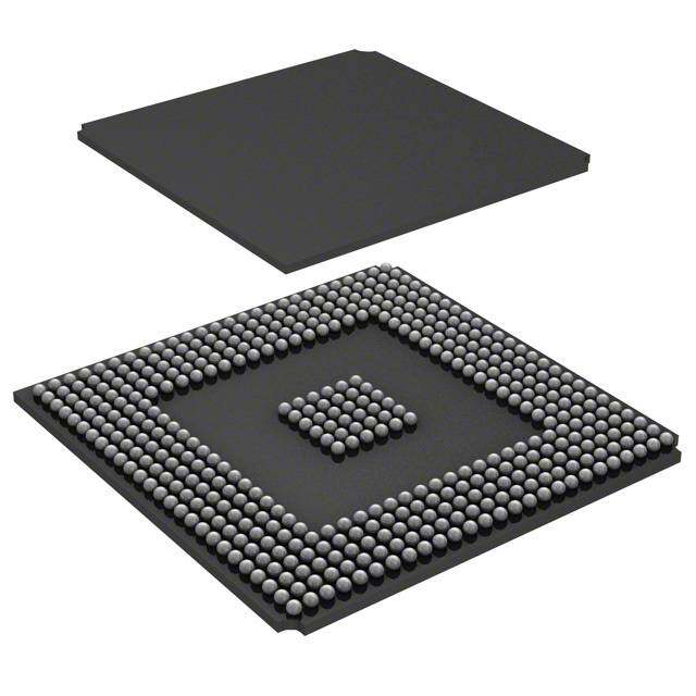
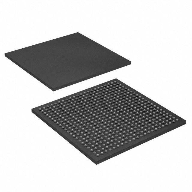
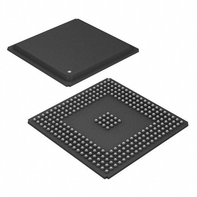
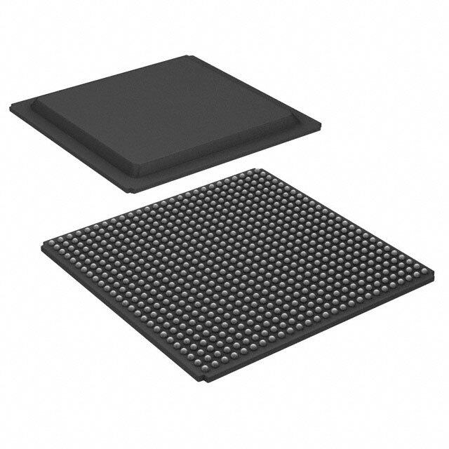
| 描述 | IC FPGA 280 I/O 484FBGAFPGA - 现场可编程门阵列 FPGA - Cyclone IV E 7155 LABs 280 IOs |
| 产品分类 | |
| I/O数 | 280 |
| LAB/CLB数 | 7155 |
| 品牌 | Altera |
| 产品手册 | |
| 产品图片 |
|
| rohs | 符合RoHS无铅 / 符合限制有害物质指令(RoHS)规范要求 |
| 产品系列 | 嵌入式处理器和控制器,FPGA - 现场可编程门阵列,Altera Corporation EP4CE115F23I7NCyclone® IV E |
| mouser_ship_limit | 根据美国政府的出口法规规定,Mouser无法将此产品销售到您所在的国家。 |
| 数据手册 | 点击此处下载产品Datasheet点击此处下载产品Datasheet点击此处下载产品Datasheet点击此处下载产品Datasheet点击此处下载产品Datasheet |
| 产品型号 | EP4CE115F23I7N |
| 产品 | Cyclone IV E |
| 产品培训模块 | http://www.digikey.cn/PTM/IndividualPTM.page?site=cn&lang=zhs&ptm=25450http://www.digikey.cn/PTM/IndividualPTM.page?site=cn&lang=zhs&ptm=25942 |
| 产品种类 | FPGA - 现场可编程门阵列 |
| 供应商器件封装 | 484-FBGA(23x23) |
| 其它名称 | 544-2806 |
| 商标 | Altera Corporation |
| 安装类型 | 表面贴装 |
| 安装风格 | SMD/SMT |
| 封装 | Tray |
| 封装/外壳 | 484-BGA |
| 封装/箱体 | FBGA-484 |
| 工作温度 | -40°C ~ 100°C |
| 工作电源电压 | 1 V to 1.2 V |
| 工厂包装数量 | 60 |
| 总RAM位数 | 3981312 |
| 总内存 | 3888 kbit |
| 最大工作温度 | + 85 C |
| 最大工作频率 | 200 MHz |
| 最小工作温度 | - 40 C |
| 栅极数 | - |
| 标准包装 | 60 |
| 特色产品 | http://www.digikey.com/product-highlights/cn/zh/altera-cyclone-iv-fpga/1886 |
| 电压-电源 | 1.15 V ~ 1.25 V |
| 系列 | Cyclone IV E |
| 输入/输出端数量 | 280 |
| 逻辑元件/单元数 | 114480 |
| 逻辑元件数量 | 114480 |
| 逻辑数组块数量——LAB | 7155 |


- 商务部:美国ITC正式对集成电路等产品启动337调查
- 曝三星4nm工艺存在良率问题 高通将骁龙8 Gen1或转产台积电
- 太阳诱电将投资9.5亿元在常州建新厂生产MLCC 预计2023年完工
- 英特尔发布欧洲新工厂建设计划 深化IDM 2.0 战略
- 台积电先进制程称霸业界 有大客户加持明年业绩稳了
- 达到5530亿美元!SIA预计今年全球半导体销售额将创下新高
- 英特尔拟将自动驾驶子公司Mobileye上市 估值或超500亿美元
- 三星加码芯片和SET,合并消费电子和移动部门,撤换高东真等 CEO
- 三星电子宣布重大人事变动 还合并消费电子和移动部门
- 海关总署:前11个月进口集成电路产品价值2.52万亿元 增长14.8%

PDF Datasheet 数据手册内容提取
1. Cyclone IV FPGA Device Family Overview March 2016 CYIV-51001-2.0 CYIV-51001-2.0 Altera’s new Cyclone®IV FPGA device family extends the Cyclone FPGA series leadership in providing the market’s lowest-cost, lowest-power FPGAs, now with a transceiver variant. CycloneIV devices are targeted to high-volume, cost-sensitive applications, enabling system designers to meet increasing bandwidth requirements while lowering costs. Built on an optimized low-power process, the CycloneIV device family offers the following two variants: ■ CycloneIV E—lowest power, high functionality with the lowest cost ■ CycloneIV GX—lowest power and lowest cost FPGAs with 3.125Gbps transceivers 1 CycloneIVE devices are offered in core voltage of 1.0V and 1.2V. f For more information, refer to the Power Requirements for CycloneIV Devices chapter. Providing power and cost savings without sacrificing performance, along with a low-cost integrated transceiver option, CycloneIV devices are ideal for low-cost, small-form-factor applications in the wireless, wireline, broadcast, industrial, consumer, and communications industries. Cyclone IV Device Family Features The CycloneIV device family offers the following features: ■ Low-cost, low-power FPGA fabric: ■ 6K to 150K logic elements ■ Up to 6.3Mb of embedded memory ■ Up to 360 18 × 18 multipliers for DSP processing intensive applications ■ Protocol bridging applications for under 1.5W total power © 2016 Altera Corporation. All rights reserved. ALTERA, ARRIA, CYCLONE, HARDCOPY, MAX, MEGACORE, NIOS, QUARTUS and STRATIX words and logos are trademarks of Altera Corporation and registered in the U.S. Patent and Trademark Office and in other countries. All other words and logos identified as trademarks or service marks are the property of their respective holders as described at www.altera.com/common/legal.html. Altera warrants performance of its ISO semiconductor products to current specifications in accordance with Altera's standard warranty, but reserves the right to make changes to any products and 9001:2008 services at any time without notice. Altera assumes no responsibility or liability arising out of the application or use of any information, product, or service Registered described herein except as expressly agreed to in writing by Altera. Altera customers are advised to obtain the latest version of device specifications before relying on any published information and before placing orders for products or services. Cyclone IV Device Handbook, Volume 1 March 2016 Feedback Subscribe
1–2 Chapter 1: CycloneIV FPGA Device Family Overview Cyclone IV Device Family Features ■ CycloneIVGX devices offer up to eight high-speed transceivers that provide: ■ Data rates up to 3.125 Gbps ■ 8B/10B encoder/decoder ■ 8-bit or 10-bit physical media attachment (PMA) to physical coding sublayer (PCS) interface ■ Byte serializer/deserializer (SERDES) ■ Word aligner ■ Rate matching FIFO ■ TX bit slipper for Common Public Radio Interface (CPRI) ■ Electrical idle ■ Dynamic channel reconfiguration allowing you to change data rates and protocols on-the-fly ■ Static equalization and pre-emphasis for superior signal integrity ■ 150 mW per channel power consumption ■ Flexible clocking structure to support multiple protocols in a single transceiver block ■ CycloneIVGX devices offer dedicated hard IP for PCI Express (PIPE) (PCIe) Gen1: ■ ×1, ×2, and ×4 lane configurations ■ End-point and root-port configurations ■ Up to 256-byte payload ■ One virtual channel ■ 2 KB retry buffer ■ 4 KB receiver (Rx) buffer ■ CycloneIVGX devices offer a wide range of protocol support: ■ PCIe (PIPE) Gen 1 ×1, ×2, and ×4 (2.5 Gbps) ■ Gigabit Ethernet (1.25 Gbps) ■ CPRI (up to 3.072Gbps) ■ XAUI (3.125 Gbps) ■ Triple rate serial digital interface (SDI) (up to 2.97Gbps) ■ Serial RapidIO (3.125 Gbps) ■ Basic mode (up to 3.125 Gbps) ■ V-by-One (up to 3.0Gbps) ■ DisplayPort (2.7Gbps) ■ Serial Advanced Technology Attachment (SATA) (up to 3.0Gbps) ■ OBSAI (up to 3.072Gbps) Cyclone IV Device Handbook, March 2016 Altera Corporation Volume 1
Chapter 1: CycloneIV FPGA Device Family Overview 1–3 Device Resources ■ Up to 532 user I/Os ■ LVDS interfaces up to 840Mbps transmitter (Tx), 875Mbps Rx ■ Support for DDR2 SDRAM interfaces up to 200MHz ■ Support for QDRII SRAM and DDR SDRAM up to 167MHz ■ Up to eight phase-locked loops (PLLs) per device ■ Offered in commercial and industrial temperature grades Device Resources Table1–1 lists CycloneIVE device resources. Table1–1. Resources for the CycloneIVE Device Family Resources EP4CE6 EP4CE10 EP4CE15 EP4CE22 EP4CE30 EP4CE40 EP4CE55 EP4CE75 EP4CE115 Logic elements (LEs) 6,272 10,320 15,408 22,320 28,848 39,600 55,856 75,408 114,480 Embedded memory 270 414 504 594 594 1,134 2,340 2,745 3,888 (Kbits) Embedded 18 × 18 15 23 56 66 66 116 154 200 266 multipliers General-purpose PLLs 2 2 4 4 4 4 4 4 4 Global Clock Networks 10 10 20 20 20 20 20 20 20 User I/O Banks 8 8 8 8 8 8 8 8 8 Maximum user I/O (1) 179 179 343 153 532 532 374 426 528 Note to Table1–1: (1) The user I/Os count from pin-out files includes all general purpose I/O, dedicated clock pins, and dual purpose configuration pins. Transceiver pins and dedicated configuration pins are not included in the pin count. March 2016 Altera Corporation Cyclone IV Device Handbook, Volume 1
1–4 Chapter 1: CycloneIV FPGA Device Family Overview Device Resources Table1–2 lists CycloneIV GX device resources. Table1–2. Resources for the CycloneIVGX Device Family Resources EP4CGX15 EP4CGX22 EP4CGX30(1) EP4CGX30(2) EP4CGX50(3) EP4CGX75(3) EP4CGX110(3) EP4CGX150(3) Logic elements (LEs) 14,400 21,280 29,440 29,440 49,888 73,920 109,424 149,760 Embedded memory (Kbits) 540 756 1,080 1,080 2,502 4,158 5,490 6,480 Embedded 18 × 18 multipliers 0 40 80 80 140 198 280 360 General purpose PLLs 1 2 2 4 (4) 4 (4) 4 (4) 4 (4) 4 (4) Multipurpose PLLs 2 (5) 2 (5) 2 (5) 2 (5) 4 (5) 4 (5) 4 (5) 4 (5) Global clock networks 20 20 20 30 30 30 30 30 High-speed transceivers (6) 2 4 4 4 8 8 8 8 Transceiver maximum data rate 2.5 2.5 2.5 3.125 3.125 3.125 3.125 3.125 (Gbps) PCIe (PIPE) hard IP blocks 1 1 1 1 1 1 1 1 User I/O banks 9 (7) 9 (7) 9 (7) 11 (8) 11 (8) 11 (8) 11 (8) 11 (8) Maximum user I/O (9) 72 150 150 290 310 310 475 475 Notes to Table1–2: (1) Applicable for the F169 and F324 packages. (2) Applicable for the F484 package. (3) Only two multipurpose PLLs for F484 package. (4) Two of the general purpose PLLs are able to support transceiver clocking. For more information, refer to the Clock Networks and PLLs in CycloneIV Devices chapter. (5) You can use the multipurpose PLLs for general purpose clocking when they are not used to clock the transceivers. For more information, refer to the Clock Networks and PLLs in CycloneIV Devices chapter. (6) If PCIe 1, you can use the remaining transceivers in a quad for other protocols at the same or different data rates. (7) Including one configuration I/O bank and two dedicated clock input I/O banks for HSSI reference clock input. (8) Including one configuration I/O bank and four dedicated clock input I/O banks for HSSI reference clock input. (9) The user I/Os count from pin-out files includes all general purpose I/O, dedicated clock pins, and dual purpose configuration pins. Transceiver pins and dedicated configuration pins are not included in the pin count. Cyclone IV Device Handbook, March 2016 Altera Corporation Volume 1
M Package Matrix PC arch 2016 Table1–3 lists CycloneIV E device package offerings. ackage Mahapter 1: A Table1–3. Package Offerings for the CycloneIVE Device Family(1), (2) trixCyc ltera lone Corpora SPiazec k(magme) 22E 1×4 242 M8 1×6 84 M9 2x5 96 1U4 2×5 164 17F 2×5 167 1F93 x2 149 1U9 4×8 149 23F 4×8 243 29F 7×8 209 IV FPGA tio D n e Pitch (mm) 0.5 0.5 0.5 0.8 1.0 1.0 0.8 1.0 1.0 vic e F Device ser I/O (3)VDS ser I/O (3)VDS ser I/O (3)VDS ser I/O (3)VDS ser I/O (3)VDS ser I/O (3)VDS ser I/O (3)VDS ser I/O (3)VDS ser I/O (3)VDS amily O U L U L U L U L U L U L U L U L U L ve EP4CE6 91 21 — — — — 179 66 179 66 — — — — — — — — rvie w EP4CE10 91 21 — — — — 179 66 179 66 — — — — — — — — EP4CE15 81 18 89 21 165 53 165 53 165 53 — — — — 343 137 — — EP4CE22 79 17 — — — — 153 52 153 52 — — — — — — — — EP4CE30 — — — — — — — — — — 193 68 — — 328 124 532 224 EP4CE40 — — — — — — — — — — 193 68 328 124 328 124 532 224 EP4CE55 — — — — — — — — — — — — 324 132 324 132 374 160 EP4CE75 — — — — — — — — — — — — 292 110 292 110 426 178 EP4CE115 — — — — — — — — — — — — — — 280 103 528 230 Notes to Table1–3: (1) The E144 package has an exposed pad at the bottom of the package. This exposed pad is a ground pad that must be connected to the ground plane of your PCB. Use this exposed pad for electrical connectivity and not for thermal purposes. (2) Use the Pin Migration View window in Pin Planner of the QuartusII software to verify the pin migration compatibility when you perform device migration. For more information, refer to the I/O Management chapter in volume 2 of the QuartusII Handbook. (3) This includes both dedicated and emulated LVDS pairs. For more information, refer to the I/O Features in CycloneIV Devices chapter. C y c lo n e IV D e v ic e H Va on lume 1dbook, 1–5
VC Table1–4 lists CycloneIV GX device package offerings, including I/O and transceiver counts. 1 oy – lumclo 6 n e 1e IV Table1–4. Package Offerings for the CycloneIVGX Device Family(1) D ev Package F169 F324 F484 F672 F896 ic e Ha Size (mm) 14 × 14 19 × 19 23 × 23 27 × 27 31 × 31 n d b oo Pitch (mm) 1.0 1.0 1.0 1.0 1.0 k , Device r I/O (2)S VRs r I/O (2)S VRs r I/O (2)S VRs r I/O (2)S VRs r I/O (2)S VRs e D C e D C e D C e D C e D C Us LV X Us LV X Us LV X Us LV X Us LV X EP4CGX15 72 25 2 — — — — — — — — — — — — EP4CGX22 72 25 2 150 64 4 — — — — — — — — — EP4CGX30 72 25 2 150 64 4 290 130 4 — — — — — — EP4CGX50 — — — — — — 290 130 4 310 140 8 — — — EP4CGX75 — — — — — — 290 130 4 310 140 8 — — — EP4CGX110 — — — — — — 270 120 4 393 181 8 475 220 8 EP4CGX150 — — — — — — 270 120 4 393 181 8 475 220 8 Note to Table1–4: (1) Use the Pin Migration View window in Pin Planner of the QuartusII software to verify the pin migration compatibility when you perform device migration. For more information, refer to the I/O Management chapter in volume 2 of the QuartusII Handbook. (2) This includes both dedicated and emulated LVDS pairs. For more information, refer to the I/O Features in CycloneIV Devices chapter. C h a p te r 1 : C y c lo n e M IV a F rch PG 20 A D 1 e 6 v ic Altera Corp Packagee Family Ov oration Matrixerview
Chapter 1: CycloneIV FPGA Device Family Overview 1–7 CycloneIV Device Family Speed Grades Cyclone IV Device Family Speed Grades Table1–5 lists the CycloneIVGX devices speed grades. Table1–5. Speed Grades for the CycloneIVGX Device Family Device F169 F324 F484 F672 F896 EP4CGX15 C6, C7, C8, I7 — — — — EP4CGX22 C6, C7, C8, I7 C6, C7, C8, I7 — — — EP4CGX30 C6, C7, C8, I7 C6, C7, C8, I7 C6, C7, C8, I7 — — EP4CGX50 — — C6, C7, C8, I7 C6, C7, C8, I7 — EP4CGX75 — — C6, C7, C8, I7 C6, C7, C8, I7 — EP4CGX110 — — C7, C8, I7 C7, C8, I7 C7, C8, I7 EP4CGX150 — — C7, C8, I7 C7, C8, I7 C7, C8, I7 Table1–6 lists the CycloneIVE devices speed grades. Table1–6. Speed Grades for the CycloneIVE Device Family(1),(2) Device E144 M164 M256 U256 F256 F324 U484 F484 F780 C8L, C9L, I8L C8L, C9L, I8L EP4CE6 C6, C7, C8, I7, — — I7N C6, C7, C8, I7, — — — — A7 A7 C8L, C9L, I8L C8L, C9L, I8L EP4CE10 C6, C7, C8, I7, — — I7N C6, C7, C8, I7, — — — — A7 A7 C8L, C9L, I8L C8L, C9L, I8L C8L, C9L, I8L EP4CE15 I7N C7N, I7N I7N C6, C7, C8, I7, — — C6, C7, C8, I7, — C6, C7, C8, I7 A7 A7 C8L, C9L, I8L C8L, C9L, I8L EP4CE22 C6, C7, C8, I7, — — I7N C6, C7, C8, I7, — — — — A7 A7 C8L, C9L, I8L C8L, C9L, I8L EP4CE30 — — — — — A7N — C6, C7, C8, I7, C6, C7, C8, I7 A7 C8L, C9L, I8L C8L, C9L, I8L EP4CE40 — — — — — A7N I7N C6, C7, C8, I7, C6, C7, C8, I7 A7 C8L, C9L, I8L C8L, C9L, I8L EP4CE55 — — — — — — I7N C6, C7, C8, I7 C6, C7, C8, I7 C8L, C9L, I8L C8L, C9L, I8L EP4CE75 — — — — — — I7N C6, C7, C8, I7 C6, C7, C8, I7 C8L, C9L, I8L C8L, C9L, I8L EP4CE115 — — — — — — — C7, C8, I7 C7, C8, I7 Notes to Table1–6: (1) C8L, C9L, and I8L speed grades are applicable for the 1.0-V core voltage. (2) C6, C7, C8, I7, and A7 speed grades are applicable for the 1.2-V core voltage. March 2016 Altera Corporation Cyclone IV Device Handbook, Volume 1
1–8 Chapter 1: CycloneIV FPGA Device Family Overview CycloneIV Device Family Architecture Cyclone IV Device Family Architecture This section describes CycloneIV device architecture and contains the following topics: ■ “FPGA Core Fabric” ■ “I/O Features” ■ “Clock Management” ■ “External Memory Interfaces” ■ “Configuration” ■ “High-Speed Transceivers (CycloneIV GX Devices Only)” ■ “Hard IP for PCI Express (CycloneIV GX Devices Only)” FPGA Core Fabric CycloneIV devices leverage the same core fabric as the very successful Cyclone series devices. The fabric consists of LEs, made of 4-input look up tables (LUTs), memory blocks, and multipliers. Each CycloneIV device M9K memory block provides 9 Kbits of embedded SRAM memory. You can configure the M9K blocks as single port, simple dual port, or true dual port RAM, as well as FIFO buffers or ROM. They can also be configured to implement any of the data widths in Table1–7. Table1–7. M9K Block Data Widths for CycloneIV Device Family Mode Data Width Configurations Single port or simple dual port ×1, ×2, ×4, ×8/9, ×16/18, and ×32/36 True dual port ×1, ×2, ×4, ×8/9, and ×16/18 The multiplier architecture in CycloneIV devices is the same as in the existing Cyclone series devices. The embedded multiplier blocks can implement an 18 × 18 or two 9 × 9 multipliers in a single block. Altera offers a complete suite of DSP IP including finite impulse response (FIR), fast Fourier transform (FFT), and numerically controlled oscillator (NCO) functions for use with the multiplier blocks. The Quartus®II design software’s DSP Builder tool integrates MathWorks Simulink and MATLAB design environments for a streamlined DSP design flow. f For more information, refer to the Logic Elements and Logic Array Blocks in CycloneIV Devices, Memory Blocks in CycloneIV Devices, and Embedded Multipliers in CycloneIV Devices chapters. Cyclone IV Device Handbook, March 2016 Altera Corporation Volume 1
Chapter 1: CycloneIV FPGA Device Family Overview 1–9 CycloneIV Device Family Architecture I/O Features CycloneIV device I/O supports programmable bus hold, programmable pull-up resistors, programmable delay, programmable drive strength, programmable slew-rate control to optimize signal integrity, and hot socketing. CycloneIV devices support calibrated on-chip series termination (Rs OCT) or driver impedance matching (Rs) for single-ended I/O standards. In CycloneIV GX devices, the high-speed transceiver I/Os are located on the left side of the device. The top, bottom, and right sides can implement general-purpose user I/Os. Table1–8 lists the I/O standards that CycloneIV devices support. Table1–8. I/O Standards Support for the CycloneIV Device Family Type I/O Standard Single-Ended I/O LVTTL, LVCMOS, SSTL, HSTL, PCI, and PCI-X Differential I/O SSTL, HSTL, LVPECL, BLVDS, LVDS, mini-LVDS, RSDS, and PPDS The LVDS SERDES is implemented in the core of the device using logic elements. f For more information, refer to the I/O Features in CycloneIV Devices chapter. Clock Management CycloneIV devices include up to 30 global clock (GCLK) networks and up to eight PLLs with five outputs per PLL to provide robust clock management and synthesis. You can dynamically reconfigure CycloneIV device PLLs in user mode to change the clock frequency or phase. CycloneIV GX devices support two types of PLLs: multipurpose PLLs and general- purpose PLLs: ■ Use multipurpose PLLs for clocking the transceiver blocks. You can also use them for general-purpose clocking when they are not used for transceiver clocking. ■ Use general purpose PLLs for general-purpose applications in the fabric and periphery, such as external memory interfaces. Some of the general purpose PLLs can support transceiver clocking. f For more information, refer to the Clock Networks and PLLs in CycloneIV Devices chapter. External Memory Interfaces CycloneIV devices support SDR, DDR, DDR2 SDRAM, and QDRII SRAM interfaces on the top, bottom, and right sides of the device. CycloneIV E devices also support these interfaces on the left side of the device. Interfaces may span two or more sides of the device to allow more flexible board design. The Altera® DDRSDRAM memory interface solution consists of a PHY interface and a memory controller. Altera supplies the PHY IP and you can use it in conjunction with your own custom memory controller or an Altera-provided memory controller. CycloneIV devices support the use of error correction coding (ECC) bits on DDR and DDR2 SDRAM interfaces. March 2016 Altera Corporation Cyclone IV Device Handbook, Volume 1
1–10 Chapter 1: CycloneIV FPGA Device Family Overview CycloneIV Device Family Architecture f For more information, refer to the External Memory Interfaces in CycloneIV Devices chapter. Configuration CycloneIV devices use SRAM cells to store configuration data. Configuration data is downloaded to the CycloneIV device each time the device powers up. Low-cost configuration options include the Altera EPCS family serial flash devices and commodity parallel flash configuration options. These options provide the flexibility for general-purpose applications and the ability to meet specific configuration and wake-up time requirements of the applications. Table1–9 lists which configuration schemes are supported by CycloneIV devices. Table1–9. Configuration Schemes for CycloneIV Device Family Devices Supported Configuration Scheme CycloneIV GX AS, PS, JTAG, and FPP (1) CycloneIV E AS, AP, PS, FPP, and JTAG Note to Table1–9: (1) The FPP configuration scheme is only supported by the EP4CGX30F484 and EP4CGX50/75/110/150 devices. IEEE 1149.6 (AC JTAG) is supported on all transceiver I/O pins. All other pins support IEEE 1149.1 (JTAG) for boundary scan testing. f For more information, refer to the JTAG Boundary-Scan Testing for CycloneIV Devices chapter. For CycloneIVGX devices to meet the PCIe 100ms wake-up time requirement, you must use passive serial (PS) configuration mode for the EP4CGX15/22/30 devices and use fast passive parallel (FPP) configuration mode for the EP4CGX30F484 and EP4CGX50/75/110/150 devices. f For more information, refer to the Configuration and Remote System Upgrades in CycloneIV Devices chapter. The cyclical redundancy check (CRC) error detection feature during user mode is supported in all CycloneIVGX devices. For CycloneIVE devices, this feature is only supported for the devices with the core voltage of 1.2V. f For more information about CRC error detection, refer to the SEU Mitigation in CycloneIV Devices chapter. High-Speed Transceivers (Cyclone IV GX Devices Only) CycloneIV GX devices contain up to eight full duplex high-speed transceivers that can operate independently. These blocks support multiple industry-standard communication protocols, as well as Basic mode, which you can use to implement your own proprietary protocols. Each transceiver channel has its own pre-emphasis and equalization circuitry, which you can set at compile time to optimize signal integrity and reduce bit error rates. Transceiver blocks also support dynamic reconfiguration, allowing you to change data rates and protocols on-the-fly. Cyclone IV Device Handbook, March 2016 Altera Corporation Volume 1
Chapter 1: CycloneIV FPGA Device Family Overview 1–11 CycloneIV Device Family Architecture Figure1–1 shows the structure of the CycloneIV GX transceiver. Figure1–1. Transceiver Channel for the CycloneIVGX Device FPGA Transmitter Channel PCS Transceiver Channel Fabric PMA CoTmXpF PeIFnhOsaasteio n Byte Serializer 8B10B Encoder Serializer tx_dataout P PCI Express hard I PIPE Interface Receiver Channel PCS ReceivePrM CAhannel RX Phase Compensation FIFO Byte Ordering Byte Deserializer 8B10B Decoder Rate Match FIFO Word Aligner Deserializer CDR rx_datain f For more information, refer to the CycloneIV Transceivers Architecture chapter. Hard IP for PCI Express (Cyclone IV GX Devices Only) CycloneIV GX devices incorporate a single hard IP block for ×1, ×2, or ×4 PCIe(PIPE) in each device. This hard IP block is a complete PCIe(PIPE) protocol solution that implements the PHY-MAC layer, Data Link Layer, and Transaction Layer functionality. The hard IP for the PCIe (PIPE) block supports root-port and end-point configurations. This pre-verified hard IP block reduces risk, design time, timing closure, and verification. You can configure the block with the Quartus II software’s PCI Express Compiler, which guides you through the process step by step. f For more information, refer to the PCI Express Compiler User Guide. March 2016 Altera Corporation Cyclone IV Device Handbook, Volume 1
1–12 Chapter 1: CycloneIV FPGA Device Family Overview Reference and Ordering Information Reference and Ordering Information Figure1–2 shows the ordering codes for CycloneIVGX devices. Figure1–2. Packaging Ordering Information for the CycloneIVGX Device Member Code Package Type 15 : 14,400 logic elements F : FineLine BGA (FBGA) 22 : 21,280 logic elements N : Quad Flat Pack No Lead (QFN) 30 : 29,440 logic elements 50 : 49,888 logic elements Operating Temperature 75 : 73,920 logic elements C : Commercial temperature (T = 0° C to 85° C) 110 : 109,424 logic elements J I : Industrial temperature (T = -40° C to 100° C) 150 : 149,760 logic elements J Family Signature EP4C GX 30 C F 19 C 7 N Optional Suffix EP4C : Cyclone IV Indicates specific device options or shipment method Family Variant Package Code N : Lead-free packaging GX : 3-Gbps transceivers FBGA Package Type ES : Engineering sample Transceiver Count 14 : 169 pins Speed Grade 19 : 324 pins B : 2 23 : 484 pins 6 (fastest) C : 4 27 : 672 pins 7 D : 8 31 : 896 pins 8 Figure1–3 shows the ordering codes for CycloneIVE devices. Figure1–3. Packaging Ordering Information for the CycloneIVE Device Package Type F : FineLine BGA (FBGA) E : Enhanced Thin Quad Flat Pack (EQFP) Operating Temperature U : Ultra FineLine BGA (UBGA) M : Micro FineLine BGA (MBGA) C : Commercial temperature (TJ = 0° C to 85° C) I : Industrial temperature (T = -40° C to 100° C) J Extended industrial temperature (T = -40° C to 125° C) Family Variant J A : Automotive temperature (T = -40° C to 125° C) E : Enhanced logic/memory J Family Signature EP4C E 40 F 29 C 8 N Optional Suffix EP4C : Cyclone IV Indicates specific device options or shipment method Package Code Member Code N : Lead-free packaging FBGA Package Type ES : Engineering sample 6 : 6,272 logic elements 17 : 256 pins L : Low-voltage device 10 : 10,320 logic elements 19 : 324 pins 15 : 15,408 logic elements 23 : 484 pins Speed Grade 22 : 22,320 logic elements 29 : 780 pins 6 (fastest) 30 : 28,848 logic elements 40 : 39,600 logic elements EQFP Package Type 7 55 : 55,856 logic elements 22 : 144 pins 8 9 75 : 75,408 logic elements UBGA Package Type 115 : 114,480 logic elements 14 : 256 pins 19 : 484 pins MBGA Package Type 8 : 164 pins 9 : 256 pins Cyclone IV Device Handbook, March 2016 Altera Corporation Volume 1
Chapter 1: CycloneIV FPGA Device Family Overview 1–13 Document Revision History Document Revision History Table1–10 lists the revision history for this chapter. Table1–10. Document Revision History Date Version Changes ■ Updated Table1–4 and Table1–5 to remove support for the N148 package. March 2016 2.0 ■ Updated Figure1–2 to remove support for the N148 package. April 2014 1.9 Updated “Packaging Ordering Information for the CycloneIVE Device”. Updated Table1–3, Table1–6 and Figure1–3 to add new device options and May 2013 1.8 packages. Updated Table1–3, Table1–6 and Figure1–3 to add new device options and February 2013 1.7 packages. October 2012 1.6 Updated Table1–3 and Table1–4. ■ Updated “Cyclone IV Device Family Features” section. November 2011 1.5 ■ Updated Figure1–2 and Figure1–3. ■ Updated for the QuartusII software version 10.1 release. ■ Added CycloneIVE new device package information. December 2010 1.4 ■ Updated Table1–1, Table1–2, Table1–3, Table1–5, and Table1–6. ■ Updated Figure1–3. ■ Minor text edits. July 2010 1.3 Updated Table1–2 to include F484 package information. ■ Updated Table1–3 and Table1–6. March 2010 1.2 ■ Updated Figure1–3. ■ Minor text edits. ■ Added CycloneIVE devices in Table1–1, Table1–3, and Table1–6 for the QuartusII software version 9.1 SP1 release. ■ Added the “CycloneIV Device Family Speed Grades” and “Configuration” sections. February 2010 1.1 ■ Added Figure1–3 to include CycloneIVE Device Packaging Ordering Information. ■ Updated Table1–2, Table1–4, and Table1–5 for CycloneIVGX devices. ■ Minor text edits. November 2009 1.0 Initial release. March 2016 Altera Corporation Cyclone IV Device Handbook, Volume 1
1–14 Chapter 1: CycloneIV FPGA Device Family Overview Document Revision History Cyclone IV Device Handbook, March 2016 Altera Corporation Volume 1
Mouser Electronics Authorized Distributor Click to View Pricing, Inventory, Delivery & Lifecycle Information: I ntel: EP4CGX110DF27C8 EP4CGX75CF23C6N EP4CE6F17C7 EP4CGX150DF31C7N EP4CGX30CF23C7 EP4CGX110CF23C7N EP4CE115F29C9L EP4CE22E22I7 EP4CE10E22C9L EP4CGX22BF14C8 EP4CGX30CF19C6 EP4CGX110DF27I7N EP4CGX50CF23I7N EP4CE10F17I8LN EP4CE75F29C7N EP4CE115F29I7N EP4CE6F17I8L EP4CE22E22C6 EP4CGX75DF27C7N EP4CE6E22C8N EP4CE22F17C8L EP4CE115F23I7 EP4CGX150CF23C8N EP4CE75F29I8LN EP4CGX50CF23C8 EP4CGX15BF14C8N EP4CE75F23C8N EP4CE22F17C9L EP4CGX15BF14C7 EP4CGX75CF23C8N EP4CGX30CF23C8N EP4CE75F29C6 EP4CE10F17C7N EP4CE10F17C6 EP4CGX150DF31I7N EP4CE6E22C8 EP4CGX150DF27I7 EP4CE75F23C8 EP4CE115F23C8N EP4CE6E22C6N EP4CE10F17I7 EP4CE22F17C7 EP4CE6E22I7N EP4CGX50DF27C8N EP4CGX22BF14C6N EP4CE6E22I8LN EP4CGX110DF27C7N EP4CE10E22C8 EP4CGX30CF19I7N EP4CE6F17A7N EP4CE22E22C8N EP4CGX30BF14I7N EP4CGX75DF27C6 EP4CE10F17C9LN EP4CE75F23C8LN EP4CE115F23C9LN EP4CGX15BF14C8 EP4CGX110DF31C8N EP4CGX50DF27C7N EP4CE75F23I7 EP4CE10E22I7N EP4CE22U14I7N EP4CE22E22C9LN EP4CGX22BF14C6 EP4CGX50CF23C7N EP4CE22F17C8 EP4CE75F23I8LN EP4CE10F17A7N EP4CE6F17C9L EP4CGX15BF14C6N EP4CGX30CF19I7 EP4CE75F29C7 EP4CGX30CF23C6N EP4CGX110DF31I7N EP4CE6F17I7N EP4CE22E22C8LN EP4CGX30CF19C7N EP4CE115F23I8LN EP4CGX50DF27C7 EP4CGX150DF27C7 EP4CGX110DF31C8 EP4CE75F23C6 EP4CGX75CF23C8 EP4CE22E22C7N EP4CE22F17C6N EP4CE115F23C7N EP4CE115F23C8LN EP4CE75F29C9LN EP4CE10E22C7N EP4CGX110DF31I7 EP4CGX75DF27I7 EP4CE10E22C6N EP4CGX15BN11I7N EP4CGX50CF23C7 EP4CE115F23C8L EP4CE10F17C9L EP4CE22F17I7 EP4CGX110CF23C8N EP4CE6E22A7N EP4CGX30CF23I7N