ICGOO在线商城 > 集成电路(IC) > 数据采集 - 数模转换器 > DAC8531IDRBT
 Datasheet下载
- 型号: DAC8531IDRBT
- 制造商: Texas Instruments
- 库位|库存: xxxx|xxxx
- 要求:
| 数量阶梯 | 香港交货 | 国内含税 |
| +xxxx | $xxxx | ¥xxxx |
查看当月历史价格
查看今年历史价格
DAC8531IDRBT产品简介:
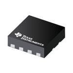
ICGOO电子元器件商城为您提供DAC8531IDRBT由Texas Instruments设计生产,在icgoo商城现货销售,并且可以通过原厂、代理商等渠道进行代购。 DAC8531IDRBT价格参考¥30.53-¥56.99。Texas InstrumentsDAC8531IDRBT封装/规格:数据采集 - 数模转换器, 16 位 数模转换器 1 8-SON-EP(3x3)。您可以下载DAC8531IDRBT参考资料、Datasheet数据手册功能说明书,资料中有DAC8531IDRBT 详细功能的应用电路图电压和使用方法及教程。
Texas Instruments 的 DAC8531IDRBT 是一款 16 位、单通道、电压输出型数模转换器(DAC),具有高精度和低功耗特性,适用于多种工业与精密控制场景。

其主要应用场景包括:

1. 工业自动化控制:用于精确控制模拟信号输出,如调节阀门、电机速度或温度控制系统中的设定点。

2. 测试与测量设备:在精密仪器中提供高分辨率的模拟电压输出,用于校准或信号模拟。

3. 医疗设备:如病人监护仪或诊断设备中,用于生成精确的模拟信号以驱动传感器或显示模块。

4. 通信系统:用于信号调节或偏置控制,确保射频或光模块工作在最佳状态。

5. 过程控制系统:在PLC(可编程逻辑控制器)或其他闭环控制系统中,将数字控制信号转换为模拟控制电压。

6. 音频与信号发生器:适用于需要高质量模拟信号输出的音频测试或信号源设备。

该器件采用小型TSSOP封装,支持I²C接口通信,适合嵌入式系统集成,且具备断电保护功能,提高了系统可靠性。
| 参数 | 数值 |
| 产品目录 | 集成电路 (IC)半导体 |
| 描述 | IC DAC 16BIT RRO LP 8SON数模转换器- DAC Lo-Pwr R-to-R Out 16-Bit Serial Input |
| 产品分类 | |
| 品牌 | Texas Instruments |
| 产品手册 | |
| 产品图片 |
|
| rohs | 符合RoHS无铅 / 符合限制有害物质指令(RoHS)规范要求 |
| 产品系列 | 数据转换器IC,数模转换器- DAC,Texas Instruments DAC8531IDRBT- |
| 数据手册 | |
| 产品型号 | DAC8531IDRBT |
| PCN设计/规格 | |
| 产品培训模块 | http://www.digikey.cn/PTM/IndividualPTM.page?site=cn&lang=zhs&ptm=13240 |
| 产品种类 | 数模转换器- DAC |
| 位数 | 16 |
| 供应商器件封装 | 8-SON 裸露焊盘(3x3) |
| 其它名称 | 296-15727-1 |
| 分辨率 | 16 bit |
| 制造商产品页 | http://www.ti.com/general/docs/suppproductinfo.tsp?distId=10&orderablePartNumber=DAC8531IDRBT |
| 包装 | 剪切带 (CT) |
| 单位重量 | 23 mg |
| 商标 | Texas Instruments |
| 安装类型 | 表面贴装 |
| 安装风格 | SMD/SMT |
| 封装 | Reel |
| 封装/外壳 | 8-VDFN 裸露焊盘 |
| 封装/箱体 | VSON-8 |
| 工作温度 | -40°C ~ 105°C |
| 工厂包装数量 | 250 |
| 建立时间 | 8µs |
| 接口类型 | QSPI, SPI, Serial (3-Wire, Microwire) |
| 数据接口 | 串行 |
| 最大工作温度 | + 105 C |
| 最小工作温度 | - 40 C |
| 标准包装 | 1 |
| 电压参考 | External |
| 电压源 | 单电源 |
| 电源电压-最大 | 5.5 V |
| 电源电压-最小 | 2.7 V |
| 积分非线性 | +/- 0.096 % FSR |
| 稳定时间 | 10 us |
| 系列 | DAC8531 |
| 结构 | Resistor-String |
| 转换器数 | 1 |
| 转换器数量 | 1 |
| 输出数和类型 | 1 电压,单极1 电压,双极 |
| 输出类型 | Voltage |
| 配用 | /product-detail/zh/DAC8531EVM/296-13548-ND/486507 |
| 采样比 | 93 kSPs |
| 采样率(每秒) | 93k |


- 商务部:美国ITC正式对集成电路等产品启动337调查
- 曝三星4nm工艺存在良率问题 高通将骁龙8 Gen1或转产台积电
- 太阳诱电将投资9.5亿元在常州建新厂生产MLCC 预计2023年完工
- 英特尔发布欧洲新工厂建设计划 深化IDM 2.0 战略
- 台积电先进制程称霸业界 有大客户加持明年业绩稳了
- 达到5530亿美元!SIA预计今年全球半导体销售额将创下新高
- 英特尔拟将自动驾驶子公司Mobileye上市 估值或超500亿美元
- 三星加码芯片和SET,合并消费电子和移动部门,撤换高东真等 CEO
- 三星电子宣布重大人事变动 还合并消费电子和移动部门
- 海关总署:前11个月进口集成电路产品价值2.52万亿元 增长14.8%


PDF Datasheet 数据手册内容提取
DAC8531 SBAS192B – MARCH 2001 – REVISED JUNE 2003 Low-Power, Rail-to-Rail Output, 16-Bit Serial Input DIGITAL-TO-ANALOG CONVERTER FEATURES DESCRIPTION (cid:1) microPower OPERATION: 250µA at 5V The DAC8531 is a low-power, single, 16-bit buffered voltage output Digital-to-Analog Converter (DAC). Its on-chip preci- (cid:1) POWER-ON RESET TO ZERO sion output amplifier allows rail-to-rail output swing to be (cid:1) POWER SUPPLY: +2.7V to +5.5V achieved. The DAC8531 uses a versatile three-wire serial (cid:1) ENSURED MONOTONIC BY DESIGN interface that operates at clock rates up to 30MHz and is compatible with standard SPI™, QSPI™, Microwire™, and (cid:1) SETTLING TIME: 10µs to ±0.003 FSR Digital Signal Processor (DSP) interfaces. (cid:1) LOW-POWER SERIAL INTERFACE WITH The DAC8531 requires an external reference voltage to set SCHMITT-TRIGGERED INPUTS the output range of the DAC. The DAC8531 incorporates a (cid:1) ON-CHIP OUTPUT BUFFER AMPLIFIER, power-on reset circuit that ensures that the DAC output powers up at 0V and remains there until a valid write takes RAIL-TO-RAIL OPERATION place to the device. The DAC8531 contains a power-down (cid:1) SYNC INTERRUPT FACILITY feature, accessed over the serial interface, that reduces the (cid:1) PACKAGES: MSOP-8 and 3x3 SON-8 (same current consumption of the device to 200nA at 5V. size as QFN) The low power consumption of this part in normal operation makes it ideally suited to portable battery-operated equip- APPLICATIONS ment. The power consumption is 2mW at 5V reducing to 1µW in power-down mode. (cid:1) PROCESS CONTROL The DAC8531 is available in both MSOP-8 and 3x3 SON-8 (cid:1) DATA ACQUISITION SYSTEMS (same size as QFN) packages. (cid:1) CLOSED-LOOP SERVO-CONTROL (cid:1) PC PERIPHERALS (cid:1) PORTABLE INSTRUMENTATION (cid:1) PROGRAMMABLE ATTENUATION VDD VFB VREF Ref (+) VOUT 16-Bit DAC 16 DAC Register 16 SYNC SCLK Shift Register Power-Down Resistor Control Logic Network DIN GND Please be aware that an important notice concerning availability, standard warranty, and use in critical applications of Texas Instruments semiconductor products and disclaimers thereto appears at the end of this data sheet. All trademarks are the property of their respective owners. PRODUCTION DATA information is current as of publication date. Copyright © 2001-2003, Texas Instruments Incorporated Products conform to specifications per the terms of Texas Instruments standard warranty. Production processing does not necessarily include testing of all parameters. www.ti.com
ABSOLUTE MAXIMUM RATINGS(1) ELECTROSTATIC VDD to GND...........................................................................–0.3V to +6V DISCHARGE SENSITIVITY Digital Input Voltage to GND.................................–0.3V to +V + 0.3V DD V to GND..........................................................–0.3V to +V + 0.3V OUT DD Operating Temperature Range......................................–40°C to +105°C This integrated circuit can be damaged by ESD. Texas Instru- Storage Temperature Range.........................................–65°C to +150°C ments recommends that all integrated circuits be handled with Junction Temperature Range (T max)........................................+150°C J appropriate precautions. Failure to observe proper handling Power Dissipation........................................................(T max — T )/θ J A JA θ Thermal Impedance.........................................................206°C/W and installation procedures can cause damage. JA θ Thermal Impedance..........................................................44°C/W JC ESD damage can range from subtle performance degradation Lead Temperature, Soldering: Vapor Phase (60s)...............................................................+215°C to complete device failure. Precision integrated circuits may be Infrared (15s)........................................................................+220°C more susceptible to damage because very small parametric NOTE: (1) Stresses above those listed under “Absolute Maximum Ratings” changes could cause the device not to meet its published may cause permanent damage to the device. Exposure to absolute maximum specifications. conditions for extended periods may affect device reliability. PACKAGE/ORDERING INFORMATION MINIMUM RELATIVE DIFFERENTIAL SPECIFICATION ACCURACY NONLINEARITY PACKAGE TEMPERATURE PACKAGE ORDERING TRANSPORT PRODUCT (LSB) (LSB) PACKAGE-LEAD DESIGNATOR(1) RANGE MARKING NUMBER MEDIA, QUANTITY DAC8531E ±64 ±1 MSOP-8 DGK –40°C to +105°C D31 DAC8531E/250 Tape and Reel, 250 " " " " " " " DAC8531E/2K5 Tape and Reel, 2500 DAC8531I ±64 ±1 SON-8 DRB –40°C to +105°C D31 DAC8531IDRBT Tape and Reel, 250 DAC8531I " " " " " " DAC8531IDRBR Tape and Reel, 2500 NOTE: (1) For the most current specifications and package information, refer to our web site at www.ti.com. ELECTRICAL CHARACTERISTICS V = +2.7V to +5.5V. –40°C to +105°C, unless otherwise specified. DD DAC8531E PARAMETER CONDITIONS MIN TYP MAX UNITS STATIC PERFORMANCE(1) Resolution 16 Bits Relative Accuracy ±0.098 % of FSR Differential Nonlinearity Ensured Monotonic by Design ±1 LSB Zero Code Error All Zeroes Loaded to DAC Register +5 +20 mV Full-Scale Error All Ones Loaded to DAC Register –0.15 –1.25 % of FSR Gain Error ±1.25 % of FSR Zero Code Error Drift ±20 µV/°C Gain Temperature Coefficient ±5 ppm of FSR/°C OUTPUT CHARACTERISTICS(2) Output Voltage Range 0 V V REF Output Voltage Settling Time To ±0.003% FSR 0200 to FD00 8 10 µs H H R = 2kΩ; 0pF < C < 200pF L L R = 2kΩ; C = 500pF 12 µs L L Slew Rate 1 V/µs ∞ Capacitive Load Stability R = 470 pF L R = 2kΩ 1000 pF L Code Change Glitch Impulse 1LSB Change Around Major Carry 20 nV-s Digital Feedthrough 0.5 nV-s DC Output Impedance 1 Ω Short-Circuit Current V = +5V 50 mA DD V = +3V 20 mA DD Power-Up Time Coming Out of Power-Down Mode V = +5V 2.5 µs DD Coming Out of Power-Down Mode V = +3V 5 µs DD REFERENCE INPUT Reference Current V = V = +5V 35 45 µA REF DD V = V = +3.6V 20 30 µA REF DD Reference Input Range 0 V V DD Reference Input Impedance 150 kΩ NOTES: (1) Linearity calculated using a reduced code range of 485 to 64714; output unloaded. (2) Ensured by design and characterization, not production tested. DAC8531 2 www.ti.com SBAS192B
ELECTRICAL CHARACTERISTICS (Cont.) V = +2.7V to +5.5V. –40°C to +105°C, unless otherwise specified. DD DAC8531E PARAMETER CONDITIONS MIN TYP MAX UNITS LOGIC INPUTS(2) Input Current ±1 µA V L, Input LOW Voltage V = +5V 0.8 V IN DD V L, Input LOW Voltage V = +3V 0.6 V IN DD V H, Input HIGH Voltage V = +5V 2.4 V IN DD V H, Input HIGH Voltage V = +3V 2.1 V IN DD Pin Capacitance 3 pF POWER REQUIREMENTS V 2.7 5.5 V DD I (normal mode) DAC Active and Excluding Load Current DD V = +3.6V to +5.5V V = V and V = GND 250 400 µA DD IH DD IL V = +2.7V to +3.6V V = V and V = GND 240 390 µA DD IH DD IL I (all power-down modes) DD V = +3.6V to +5.5V V = V and V = GND 0.2 1 µA DD IH DD IL V = +2.7V to +3.6V V = V and V = GND 0.05 1 µA DD IH DD IL POWER EFFICIENCY I /I I = 2mA, V = +5V 89 % OUT DD LOAD DD TEMPERATURE RANGE Specified Performance –40 +105 °C PIN CONFIGURATIONS PIN DESCRIPTION Top View PIN NAME DESCRIPTION 1 V Power-Supply Input, +2.7V to +5.5V. DD 2 V Reference Voltage Input V 1 8 GND REF DD 3 V Feedback connection for the output amplifier. FB V 2 7 D REF DAC8531 IN 4 VOUT Analog output voltage from DAC. The output ampli- fier has rail-to-rail operation. V 3 6 SCLK FB 5 SYNC Level-triggered control input (active LOW). This is VOUT 4 5 SYNC the frame sychronization signal for the input data. When SYNC goes LOW, it enables the input shift register and data is transferred in on the falling MSOP-8 edges of the following clocks. The DAC is updated following the 24th clock cycle unless SYNC is taken HIGH before this edge, in which case the rising edge of SYNC acts as an interrupt and the write sequence is ignored by the DAC8531. 6 SCLK Serial Clock Input. Data can be transferred at rates VDD 1 8 GND up to 30MHz. 7 D Serial Data Input. Data is clocked into the 24-bit V 2 7 D IN REF DAC8531 IN input shift register on the falling edge of the serial V 3 6 SCLK clock input. FB 8 GND Ground reference point for all circuitry on the part. V 4 5 SYNC OUT SON-8 DAC8531 3 SBAS192B www.ti.com
TIMING CHARACTERISTICS(1, 2) V = +2.7V to +5.5V; all specifications –40°C to +105°C unless otherwise noted. DD DAC8531E PARAMETER DESCRIPTION CONDITIONS MIN TYP MAX UNITS t(3) SCLK Cycle Time 1 V = 2.7V to 3.6V 50 ns DD V = 3.6V to 5.5V 33 ns DD t SCLK HIGH Time 2 V = 2.7V to 3.6V 13 ns DD V = 3.6V to 5.5V 13 ns DD t SCLK LOW Time 3 V = 2.7V to 3.6V 22.5 ns DD V = 3.6V to 5.5V 13 ns DD t SYNC to SCLK Rising 4 Edge Setup Time V = 2.7V to 3.6V 0 ns DD V = 3.6V to 5.5V 0 ns DD t Data Setup Time 5 V = 2.7V to 3.6V 5 ns DD V = 3.6V to 5.5V 5 ns DD t Data Hold Time 6 V = 2.7V to 3.6V 4.5 ns DD V = 3.6V to 5.5V 4.5 ns DD t SCLK Falling Edge to 7 SYNC Rising Edge V = 2.7V to 3.6V 0 ns DD V = 3.6V to 5.5V 0 ns DD t Minimum SYNC HIGH Time 8 V = 2.7V to 3.6V 50 ns DD V = 3.6V to 5.5V 33 ns DD NOTES: (1) All input signals are specified with t = t = 5ns (10% to 90% of V ) and timed from a voltage level of (V + V )/2. (2) See Serial Write Operation timing R F DD IL IH diagram, below. (3) Maximum SCLK frequency is 30MHz at V = +3.6V to +5.5V and 20MHz at V = +2.7V to +3.6V. DD DD SERIAL WRITE OPERATION t 1 SCLK t t 8 t t3 2 t7 4 SYNC t 6 t 5 D DB23 DB0 IN DAC8531 4 www.ti.com SBAS192B
TYPICAL CHARACTERISTICS: V = 5V DD At T = +25°C, V = 5V, unless otherwise noted. A DD NOTE: All references to I include I current. DD REF LINEARITY ERROR AND LINEARITY ERROR AND DIFFERENTIAL LINEARITY ERROR vs CODE DIFFERENTIAL LINEARITY ERROR vs CODE (–40°C) (+25°C) 64 64 48 48 32 32 B) 16 B) 16 S S L 0 L 0 E ( –16 E ( –16 L –32 L –32 –48 –48 –64 –64 2.0 2.0 1.5 1.5 B) 1.0 B) 1.0 S 0.5 S 0.5 LE (L –00..50 LE (L –00..50 D –1.0 D –1.0 –1.5 –1.5 –2.0 –2.0 0000 2000 4000 6000 8000 A000 C000 E000 FFFF 0000 2000 4000 6000 8000 A000 C000 E000 FFFF H H H H H H H H H H H H H H H H H H Digital Input Code Digital Input Code LINEARITY ERROR AND DIFFERENTIAL LINEARITY ERROR vs CODE (+105°C) ZERO-SCALE ERROR vs TEMPERATURE 64 20 48 32 15 B) 16 S E (L –160 10 L –32 5 –48 V) –64 m 21..05 Error ( –05 B) 1.0 S 0.5 –10 DLE (L ––010...500 –15 –1.5 –2.0 –20 0000 2000 4000 6000 8000 A000 C000 E000 FFFF –40 0 40 80 120 H H H H H H H H H Temperature (°C) Digital Input Code FULL-SCALE ERROR vs TEMPERATURE I HISTOGRAM DD 20 2000 15 10 1500 5 V) cy m n or ( 0 que 1000 Err –5 Fre –10 500 –15 –20 0 –40 0 40 80 120 100 130 160 190 220 250 280 310 340 370 400 Temperature (°C) I (µA) DD DAC8531 5 SBAS192B www.ti.com
TYPICAL CHARACTERISTICS: V = 5V (Cont.) DD At T = +25°C, V = 5V, unless otherwise noted. A DD NOTE: All references to I include I current. DD REF SOURCE AND SINK CURRENT CAPABILITY SUPPLY CURRENT vs DIGITAL INPUT CODE 5 500 DAC Loaded with FFFF H 4 400 3 300 V (V)OUT 2 µI (A)DD 200 1 100 DAC Loaded with 0000 H 0 0 0 5 10 15 0000 2000 4000 6000 8000 A000 C000 E000 FFFF H H H H H H H H H ISOURCE/SINK (mA) Digital Input Code POWER-SUPPLY CURRENT vs TEMPERATURE SUPPLY CURRENT vs SUPPLY VOLTAGE 350 350 V tied to V . REF DD 300 300 A) µ 250 250 nt( e urr 200 A) 200 C µ cent 150 I(DD 150 s e ui 100 100 Q 50 50 0 0 –40 0 40 80 120 2.7 3.2 3.7 4.2 4.7 5.2 5.7 Temperature (°C) V (V) DD POWER-DOWN CURRENT vs SUPPLY VOLTAGE SUPPLY CURRENT vs LOGIC INPUT VOLTAGE 100 700 90 80 600 70 500 60 A) +105°C A) (nD 50 –40°C µ (D 400 D 40 D I I 30 300 20 10 +25°C 200 0 100 2.7 3.2 3.7 4.2 4.7 5.2 5.7 0 1 2 3 4 5 V (V) V (V) DD LOGIC DAC8531 6 www.ti.com SBAS192B
TYPICAL CHARACTERISTICS: V = 5V (Cont.) DD At T = +25°C, V = 5V, unless otherwise noted. A DD FULL-SCALE SETTLING TIME FULL-SCALE SETTLING TIME Scope Trigger (5.0V/div) Scope Trigger (5.0V/div) Large-Signal Output (1.0V/div) Small-Signal Error (1mV/div) Small-Signal Error (1mV/div) Full-Scale Code Change FFFF to 0000 Full-Scale Code Change H H Output Loaded with 0000H to FFFFH 2kΩ and 200pF to GND Output Loaded with 2kΩ and 200pF to GND Large-Signal Output (1.0V/div) Time (2µs/div) Time (2µs/div) HALF-SCALE SETTLING TIME HALF-SCALE SETTLING TIME Scope Trigger (5.0V/div) Scope Trigger (5.0V/div) Large-Signal Output (1.0V/div) Small-Signal Error (1mV/div) Small-Signal Error (1mV/div) Large-Signal Output (1V/div) Half-Scale Code Change 4000 to C000 Half-Scale Code Change H H Output Loaded with C000H to 4000H 2kΩ and 200pF to GND Output Loaded with 2kΩ and 200pF to GND Time (2µs/div) Time (2µs/div) EXITING POWER-DOWN POWER-ON RESET TO 0V (8000 Loaded) H Loaded with 2kΩ to VDD. Scope Trigger (5.0V/div) V (2V/div) DD Output (1.0V/div) V (1V/div) OUT Time (50µs/div) Time (2µs/div) DAC8531 7 SBAS192B www.ti.com
TYPICAL CHARACTERISTICS: V = 5V (Cont.) DD At T = +25°C, V = 5V, unless otherwise noted. A DD CODE CHANGE GLITCH v) di V/ Glitch Waveform (50mV/div) m 0 5 (T U O V Time (2µs/div) TYPICAL CHARACTERISTICS: V = 2.7V DD At T = +25°C, V = 2.7V, unless otherwise noted. A DD LINEARITY ERROR AND LINEARITY ERROR AND DIFFERENTIAL LINEARITY ERROR vs CODE DIFFERENTIAL LINEARITY ERROR vs CODE (–40°C) (+25°C) 64 64 48 48 E (LSB) –1316260 E (LSB) –1316260 L –32 L –32 –48 –48 –64 –64 2.0 2.0 1.5 1.5 SB) 10..05 SB) 10..05 DLE (L ––010...500 DLE (L ––010...500 –1.5 –1.5 –2.0 –2.0 0000H 2000H 4000H 6000H 8000H A000H C000H E000H FFFFH 0000H 2000H 4000H 6000H 8000H A000H C000H E000H FFFFH Digital Input Code Digital Input Code LINEARITY ERROR AND DIFFERENTIAL LINEARITY ERROR vs CODE (+105°C) ZERO-SCALE ERROR vs TEMPERATURE 64 20 48 32 15 B) 16 S E (L –160 10 L –32 5 –48 V) –64 m 21..05 Error ( –05 B) 1.0 DLE (LS ––0100....5050 ––1105 –1.5 –2.0 –20 0000 2000 4000 6000 8000 A000 C000 E000 FFFF –40 0 40 80 120 H H H H H H H H H Temperature (°C) Digital Input Code DAC8531 8 www.ti.com SBAS192B
TYPICAL CHARACTERISTICS: V = 2.7V DD At T = +25°C, V = 2.7V, unless otherwise noted. A DD NOTE: All references to I include I current. DD REF FULL-SCALE ERROR vs TEMPERATURE I HISTOGRAM DD 20 2000 15 10 1500 5 V) cy m n or ( 0 que 1000 Err –5 Fre –10 500 –15 –20 0 –40 0 40 80 120 100 130 160 190 220 250 280 310 340 370 400 Temperature (°C) I (µA) DD SOURCE AND SINK CURRENT CAPABILITY SUPPLY CURRENT vs DIGITAL INPUT CODE 3.0 500 2.5 400 DAC Loaded with FFFF H 2.0 300 V) A) V (OUT 1.5 µI (DD 200 1.0 100 0.5 DAC Loaded with 0000 H 0.0 0 0 5 10 15 0000H 2000H 4000H 6000H 8000H A000H C000H E000HFFFFH I (mA) Digital Input Code SOURCE/SINK POWER SUPPLY CURRENT vs TEMPERATURE SUPPLY CURRENT vs LOGIC INPUT VOLTAGE 350 200 300 180 A) µ 250 nt( 160 e ent Curr 210500 µI (A)DD 140 c es 120 ui 100 Q 100 50 0 80 –40 0 40 80 120 0 0.5 1 1.5 2 2.5 3 Temperature (°C) VLOGIC (V) DAC8531 9 SBAS192B www.ti.com
TYPICAL CHARACTERISTICS: V = 2.7V (Cont.) DD At T = +25°C, V = 2.7V, unless otherwise noted. A DD FULL-SCALE SETTLING TIME FULL-SCALE SETTLING TIME Scope Trigger (5.0V/div) Scope Trigger (5.0V/div) Large-Signal Output (1.0V/div) Small-Signal Error (1mV/div) Small-Signal Error (1mV/div) Large-Signal Output (1.0V/div) Full-Scale Code Change Full-Scale Code Change 0000H to FFFFH FFFFH to 0000H Output Loaded with Output Loaded with 2kΩ and 200pF to GND 2kΩ and 200pF to GND Time (2µs/div) Time (2µs/div) HALF-SCALE SETTLING TIME HALF-SCALE SETTLING TIME Scope Trigger (5.0V/div) Scope Trigger (5.0V/div) Large-Signal Output (1.0V/div) Small-Signal Error (1mV/div) Small-Signal Error (1mV/div) Large-Signal Output (1.0V/div) Half-Scale Code Change 4000 to C000 Half-Scale Code Change Output HLoaded wHith C000H to 4000H 2kΩ and 200pF to GND Output Loaded with 2kΩ and 200pF to GND Time (2µs/div) Time (2µs/div) EXITING POWER-DOWN POWER-ON RESET to 0V (8000 Loaded) H Loaded with 2kΩ to VDD. Scope Trigger (5.0V/div) V (1V/div) DD Output (1.0V/div) V (1V/div) OUT Time (50µs/div) Time (2µs/div) DAC8531 10 www.ti.com SBAS192B
TYPICAL CHARACTERISTICS: V = 2.7V (Cont.) DD At T = +25°C, V = 2.7V, unless otherwise noted. A DD CODE CHANGE GLITCH v) di V/ Glitch Waveform (20mV/div) m 0 2 (T U O V Time (2µs/div) THEORY OF OPERATION RESISTOR STRING Figure 2 shows the resistor string section. It is simply a string DAC SECTION of resistors, each of value R. The code loaded into the DAC The architecture consists of a string DAC followed by an register determines at which node on the string the voltage output buffer amplifier. Figure 1 shows a block diagram of the is tapped off to be fed into the output amplifier by closing one DAC architecture. of the switches connecting the string to the amplifier. It is ensured monotonic because it is a string of resistors. VDD VFB R REF (+) VOUT DAC Register Resistor String REF(–) Output Amplifier R GND To Output R Amplifier FIGURE 1. DAC8531 Architecture. The input coding to the DAC8531 is straight binary, so the ideal output voltage is given by: D V =V • OUT REF 65536 R where D = decimal equivalent of the binary code that is loaded to the DAC register; it can range from 0 to 65535. R FIGURE 2. Resistor String. DAC8531 11 SBAS192B www.ti.com
OUTPUT AMPLIFIER SYNC buffer draws more current when the SYNC signal is HIGH than it does when it is LOW, SYNC should be idled The output buffer amplifier is capable of generating rail-to-rail LOW between write sequences for lowest power operation of voltages on its output which gives an output range of 0V to V . It is capable of driving a load of 2kΩ in parallel with the part. As mentioned above, it must be brought HIGH again DD just before the next write sequence. 1000pF to GND. The source and sink capabilities of the output amplifier can be seen in the typical curves. The slew rate is 1V/µs with a full-scale settling time of 8µs with the INPUT SHIFT REGISTER output unloaded. The input shift register is 24 bits wide, as shown in Figure 3. The inverting input of the output amplifier is brought out to the The first six bits are “don’t cares”. The next two bits (PD1 and V pin. This allows for better accuracy in critical applications PD0) are control bits that control which mode of operation the FB by tying the V point and the amplifier output together part is in (normal mode or any one of three power-down FB directly at the load. Other signal conditioning circuitry modes). There is a more complete description of the various may also be connected between these points for specific modes in the Power-Down Modes section. The next 16 bits applications. are the data bits. These are transferred to the DAC register on the 24th falling edge of SCLK. SERIAL INTERFACE SYNC INTERRUPT The DAC8531 has a three-wire serial interface (SYNC, In a normal write sequence, the SYNC line is kept LOW for SCLK, and DIN), which is compatible with SPI, QSPI, and at least 24 falling edges of SCLK and the DAC is updated on Microwire interface standards as well as most DSPs. See the the 24th falling edge. However, if SYNC is brought HIGH Serial Write Operation timing diagram for an example of a before the 24th falling edge, this acts as an interrupt to the typical write sequence. write sequence. The shift register is reset and the write The write sequence begins by bringing the SYNC line LOW. sequence is seen as invalid. Neither an update of the DAC Data from the D line is clocked into the 24-bit shift register register contents or a change in the operating mode occurs, IN on the falling edge of SCLK. The serial clock frequency can as shown in Figure 4. be as high as 30MHz, making the DAC8531 compatible with high-speed (DSPs). On the 24th falling edge of the serial POWER-ON RESET clock, the last data bit is clocked in and the programmed The DAC8531 contains a power-on reset circuit that controls function is executed (i.e., a change in DAC register contents the output voltage during power-up. On power-up, the DAC and/or a change in the mode of operation). register is filled with zeros and the output voltage is 0V; it At this point, the SYNC line may be kept LOW or brought remains there until a valid write sequence is made to the HIGH. In either case, it must be brought HIGH for a minimum DAC. This is useful in applications where it is important to of 33ns before the next write sequence so that a falling edge know the state of the output of the DAC while it is in the of SYNC can initiate the next write sequence. Since the process of powering up. DB23 DB0 X X X X X X PD1 PD0 D15 D14 D13 D12 D11 D10 D9 D8 D7 D6 D5 D4 D3 D2 D1 D0 FIGURE 3. Data Input Register. 24th Falling Edge 24th Falling Edge CLK SYNC DIN DB23 DB0 DB23 DB0 Invalid Write Sequence: Valid Write Sequence: Output Updates SYNC HIGH before 24th Falling Edge on the 24th Falling Edge FIGURE 4. SYNC Interrupt Facility. DAC8531 12 www.ti.com SBAS192B
POWER-DOWN MODES MICROPROCESSOR The DAC8531 supports four separate modes of operation. INTERFACING These modes are programmable by setting two bits (PD1 and PD0) in the control register. Table I shows how the state DAC8531 TO 8051 INTERFACE of the bits corresponds to the mode of operation of the Figure 6 shows a serial interface between the DAC8531 and device. a typical 8051-type microcontroller. The setup for the inter- face is as follows: TXD of the 8051 drives SCLK of the PD1 (DB17) PD0 (DB16) OPERATING MODE DAC8531, while RXD drives the serial data line of the part. 0 0 Normal Operation The SYNC signal is derived from a bit-programmable pin on — — Power-Down Modes the port. In this case, port line P3.3 is used. When data is to 0 1 Output 1kΩ to GND be transmitted to the DAC8531, P3.3 is taken LOW. The 1 0 Output 100kΩ to GND 8051 transmits data only in 8-bit bytes; thus only eight falling 1 1 High-Z clock edges occur in the transmit cycle. To load data to the TABLE I. Modes of Operation for the DAC8531. DAC, P3.3 is left LOW after the first eight bits are transmitted and a second write cycle is initiated to transmit the second When both bits are set to 0, the part works normally with its byte of data. P3.3 is taken HIGH following the completion of typical current consumption of 250µA at 5V. However, for the the third write cycle. The 8051 outputs the serial data in a three power-down modes, the supply current falls to 200nA format which has the LSB first. The DAC8531 requires its at 5V (50nA at 3V). Not only does the supply current fall, but data with the MSB as the first bit received. The 8051 transmit the output stage is also internally switched from the output of routine must therefore take this into account, and “mirror” the the amplifier to a resistor network of known values. This has data as needed. the advantage that the output impedance of the part is known while the part is in power-down mode. There are three different options. The output is connected internally to GND through a 1kΩ resistor, a 100kΩ resistor, or it is left open- 80C51/80L51(1) DAC8531(1) circuited (High-Z). The output stage is illustrated in Figure 5. P3.3 SYNC TXD SCLK RXD D IN NOTE: (1) Additional pins omitted for clarity. V FB FIGURE 6. DAC8531 to 80C51/80L51 Interface. Amplifier V Resistor OUT String DAC DAC8531 TO Microwire INTERFACE Figure 7 shows an interface between the DAC8531 and any Power-Down Resistor Microwire compatible device. Serial data is shifted out on the Circuitry Network falling edge of the serial clock and is clocked into the DAC8531 on the rising edge of the SK signal. FIGURE 5. Output Stage During Power-Down. MicrowireTM DAC8531(1) CS SYNC All linear circuitry is shut down when the power-down mode SK SCLK is activated. However, the contents of the DAC register are unaffected when in power-down. The time to exit SO DIN power-down is typically 2.5µs for V = 5V, and 5µs DD NOTE: (1) Additional pins omitted for clarity. for V = 3V. See the Typical Characteristics for more DD Microwire is a registered trademark of National Semiconductor. information. FIGURE 7. DAC8531 to Microwire Interface. DAC8531 13 SBAS192B www.ti.com
DAC8531 TO 68HC11 INTERFACE power supply is quite noisy or if the system supply voltages Figure 8 shows a serial interface between the DAC8531 and are at some value other than 5V. The REF02 will output a the 68HC11 microcontroller. SCK of the 68HC11 drives the steady supply voltage for the DAC8531. If the REF02 is SCLK of the DAC8531, while the MOSI output drives the used, the typical current it needs to supply to the DAC8531 serial data line of the DAC. The SYNC signal is derived from is 250µA. This is with no load on the output of the DAC. a port line (PC7), similar to what was done for the 8051. When the DAC output is loaded, the REF02 also needs to supply the current to the load. The total current required (with a 5kΩ load on the DAC output) is: 250µA + (5V/5kΩ) = 1.29mA 68HC11(1) DAC8531(1) PC7 SYNC The load regulation of the REF02 is typically 0.005%/mA, SCK SCLK which results in an error of 322µV for the 1.29mA current MOSI D IN drawn from it. This corresponds to a 4.2LSB error. NOTE: (1) Additional pins omitted for clarity. BIPOLAR OPERATION USING THE DAC8531 The DAC8531 has been designed for single-supply operation FIGURE 8. DAC8531 to 68HC11 Interface. but a bipolar output range is also possible using the circuit in Figure 10. The circuit shown will give an output voltage range The 68HC11 should be configured so that its CPOL bit is a of ±V . Rail-to-rail operation at the amplifier output is achiev- REF 0 and its CPHA bit is a 1. This configuration causes data able using an OPA703 as the output amplifier. appearing on the MOSI output to be valid on the falling edge The output voltage for any input code can be calculated as of SCK. When data is being transmitted to the DAC, the follows: SYNC line is taken LOW (PC7). Serial data from the 68HC11 is transmitted in 8-bit bytes with only eight falling clock edges D R +R R V =V • • 1 2 –V • 2 occurring in the transmit cycle. Data is transmitted MSB first. O REF 65536 R1 REF R1 In order to load data to the DAC8531, PC7 is left LOW after the first eight bits are transferred, then a second and third where D represents the input code in decimal (0–65535). serial write operation is performed to the DAC and PC7 is With V = 5V, R = R = 10kΩ: REF 1 2 taken HIGH at the end of this procedure. 10•D V = –5V O 65536 APPLICATIONS This is an output voltage range of ±5V with 0000 corre- H USING REF02 AS A POWER SUPPLY FOR sponding to a –5V output and FFFF corresponding to a +5V H THE DAC8531 output. Similarly, using V = 2.5V, ±2.5V output voltage REF Due to the extremely low supply current required by the raw can be achieved. DAC8531, an alternative option is to use a REF02 +5V precision voltage reference to supply the required voltage to LAYOUT the part, as shown in Figure 9. This is especially useful if the A precision analog component requires careful layout, ad- equate bypassing, and clean, well-regulated power supplies. +15 As the DAC8531 offers single-supply operation, it will often be used in close proximity with digital logic, microcontrollers, +5V microprocessors, and digital signal processors. The more REF02 digital logic present in the design and the higher the switch- 285µA ing speed, the more difficult it will be to keep digital noise from appearing at the output. Due to the single ground pin of the DAC8531, all return SYNC currents, including digital and analog return currents, must ThrSeeer-iWalire SCLK DAC8531 VOUT = 0V to 5V flow through the GND pin. Ideally, GND would be connected Interface directly to an analog ground plane. This plane would be D separate from the ground connection for the digital compo- IN nents until they were connected at the power-entry point of the system. FIGURE 9. REF02 as a Power Supply to the DAC8531. DAC8531 14 www.ti.com SBAS192B
The power applied to V should be well regulated and low As with the GND connection, V should be connected to a DD DD noise. Switching power supplies and DC/DC converters will +5V power-supply plane or trace that is separate from the often have high-frequency glitches or spikes riding on the connection for digital logic until they are connected at the output voltage. In addition, digital components can create power-entry point. In addition, the 1µF to 10µF and 0.1µF similar high-frequency spikes as their internal logic switches bypass capacitors are strongly recommended. In some situ- states. This noise can easily couple into the DAC output ations, additional bypassing may be required, such as a voltage through various paths between the power connec- 100µF electrolytic capacitor or even a “Pi” filter made up of tions and analog output. inductors and capacitors—all designed to essentially low- pass filter the +5V supply, removing the high-frequency noise. R 2 VREF 10kΩ +5V R 1 10kΩ OPA703 V ±5V FB VREF DAC8531 VOUT 10µF 0.1µF –5V Three-Wire Serial Interface FIGURE 10. Bipolar Operation with the DAC8531. DAC8531 15 SBAS192B www.ti.com
PACKAGE DRAWINGS DGK (R-PDSO-G8) PLASTIC SMALL-OUTLINE PACKAGE 0,38 0,65 0,08 M 0,25 8 5 0,15 NOM 3,05 4,98 2,95 4,78 Gage Plane 0,25 1 4 0°–6° 0,69 3,05 0,41 2,95 Seating Plane 0,15 1,07 MAX 0,10 0,05 4073329/C 08/01 NOTES: A. All linear dimensions are in millimeters. B. This drawing is subject to change without notice. C. Body dimensions do not include mold flash or protrusion. D. Falls within JEDEC MO-187 DAC8531 16 www.ti.com SBAS192B
PACKAGE DRAWINGS (Cont.) DAC8531 17 SBAS192B www.ti.com
PACKAGE OPTION ADDENDUM www.ti.com 6-Feb-2020 PACKAGING INFORMATION Orderable Device Status Package Type Package Pins Package Eco Plan Lead/Ball Finish MSL Peak Temp Op Temp (°C) Device Marking Samples (1) Drawing Qty (2) (6) (3) (4/5) DAC8531E/250 ACTIVE VSSOP DGK 8 250 Green (RoHS NIPDAUAG Level-2-260C-1 YEAR -40 to 105 D31 & no Sb/Br) DAC8531E/250G4 ACTIVE VSSOP DGK 8 250 Green (RoHS NIPDAUAG Level-2-260C-1 YEAR -40 to 105 D31 & no Sb/Br) DAC8531E/2K5 ACTIVE VSSOP DGK 8 2500 Green (RoHS NIPDAUAG Level-2-260C-1 YEAR -40 to 105 D31 & no Sb/Br) DAC8531E/2K5G4 ACTIVE VSSOP DGK 8 2500 Green (RoHS NIPDAUAG Level-2-260C-1 YEAR -40 to 105 D31 & no Sb/Br) DAC8531IDRBR ACTIVE SON DRB 8 3000 Green (RoHS NIPDAU Level-2-260C-1 YEAR -40 to 105 D31 & no Sb/Br) DAC8531IDRBT ACTIVE SON DRB 8 250 Green (RoHS NIPDAU Level-2-260C-1 YEAR -40 to 105 D31 & no Sb/Br) (1) The marketing status values are defined as follows: ACTIVE: Product device recommended for new designs. LIFEBUY: TI has announced that the device will be discontinued, and a lifetime-buy period is in effect. NRND: Not recommended for new designs. Device is in production to support existing customers, but TI does not recommend using this part in a new design. PREVIEW: Device has been announced but is not in production. Samples may or may not be available. OBSOLETE: TI has discontinued the production of the device. (2) RoHS: TI defines "RoHS" to mean semiconductor products that are compliant with the current EU RoHS requirements for all 10 RoHS substances, including the requirement that RoHS substance do not exceed 0.1% by weight in homogeneous materials. Where designed to be soldered at high temperatures, "RoHS" products are suitable for use in specified lead-free processes. TI may reference these types of products as "Pb-Free". RoHS Exempt: TI defines "RoHS Exempt" to mean products that contain lead but are compliant with EU RoHS pursuant to a specific EU RoHS exemption. Green: TI defines "Green" to mean the content of Chlorine (Cl) and Bromine (Br) based flame retardants meet JS709B low halogen requirements of <=1000ppm threshold. Antimony trioxide based flame retardants must also meet the <=1000ppm threshold requirement. (3) MSL, Peak Temp. - The Moisture Sensitivity Level rating according to the JEDEC industry standard classifications, and peak solder temperature. (4) There may be additional marking, which relates to the logo, the lot trace code information, or the environmental category on the device. (5) Multiple Device Markings will be inside parentheses. Only one Device Marking contained in parentheses and separated by a "~" will appear on a device. If a line is indented then it is a continuation of the previous line and the two combined represent the entire Device Marking for that device. Addendum-Page 1
PACKAGE OPTION ADDENDUM www.ti.com 6-Feb-2020 (6) Lead/Ball Finish - Orderable Devices may have multiple material finish options. Finish options are separated by a vertical ruled line. Lead/Ball Finish values may wrap to two lines if the finish value exceeds the maximum column width. Important Information and Disclaimer:The information provided on this page represents TI's knowledge and belief as of the date that it is provided. TI bases its knowledge and belief on information provided by third parties, and makes no representation or warranty as to the accuracy of such information. Efforts are underway to better integrate information from third parties. TI has taken and continues to take reasonable steps to provide representative and accurate information but may not have conducted destructive testing or chemical analysis on incoming materials and chemicals. TI and TI suppliers consider certain information to be proprietary, and thus CAS numbers and other limited information may not be available for release. In no event shall TI's liability arising out of such information exceed the total purchase price of the TI part(s) at issue in this document sold by TI to Customer on an annual basis. Addendum-Page 2
PACKAGE MATERIALS INFORMATION www.ti.com 24-Jul-2013 TAPE AND REEL INFORMATION *Alldimensionsarenominal Device Package Package Pins SPQ Reel Reel A0 B0 K0 P1 W Pin1 Type Drawing Diameter Width (mm) (mm) (mm) (mm) (mm) Quadrant (mm) W1(mm) DAC8531E/250 VSSOP DGK 8 250 180.0 12.4 5.3 3.4 1.4 8.0 12.0 Q1 DAC8531E/2K5 VSSOP DGK 8 2500 330.0 12.4 5.3 3.4 1.4 8.0 12.0 Q1 DAC8531IDRBR SON DRB 8 3000 330.0 12.4 3.3 3.3 1.1 8.0 12.0 Q2 DAC8531IDRBT SON DRB 8 250 180.0 12.4 3.3 3.3 1.1 8.0 12.0 Q2 PackMaterials-Page1
PACKAGE MATERIALS INFORMATION www.ti.com 24-Jul-2013 *Alldimensionsarenominal Device PackageType PackageDrawing Pins SPQ Length(mm) Width(mm) Height(mm) DAC8531E/250 VSSOP DGK 8 250 210.0 185.0 35.0 DAC8531E/2K5 VSSOP DGK 8 2500 367.0 367.0 35.0 DAC8531IDRBR SON DRB 8 3000 367.0 367.0 35.0 DAC8531IDRBT SON DRB 8 250 210.0 185.0 35.0 PackMaterials-Page2
None
PACKAGE OUTLINE DRB0008B VSON - 1 mm max height SCALE 4.000 PLASTIC SMALL OUTLINE - NO LEAD 3.1 B A 2.9 PIN 1 INDEX AREA 3.1 2.9 C 1 MAX SEATING PLANE 0.05 0.08 C 0.00 EXPOSED 1.65 0.05 (0.2) TYP THERMAL PAD 4 5 2X 1.95 2.4 0.05 8 1 6X 0.65 0.35 8X 0.25 PIN 1 ID 0.5 0.1 C A B (OPTIONAL) 8X 0.3 0.05 C 4218876/A 12/2017 NOTES: 1. All linear dimensions are in millimeters. Any dimensions in parenthesis are for reference only. Dimensioning and tolerancing per ASME Y14.5M. 2. This drawing is subject to change without notice. 3. The package thermal pad must be soldered to the printed circuit board for thermal and mechanical performance. www.ti.com
EXAMPLE BOARD LAYOUT DRB0008B VSON - 1 mm max height PLASTIC SMALL OUTLINE - NO LEAD (1.65) 8X (0.6) SYMM 1 8 8X (0.3) (2.4) (0.95) 6X (0.65) 4 5 (R0.05) TYP (0.575) ( 0.2) VIA (2.8) TYP LAND PATTERN EXAMPLE SCALE:20X 0.07 MAX 0.07 MIN ALL AROUND ALL AROUND SOLDER MASK METAL METAL UNDER SOLDER MASK OPENING SOLDER MASK OPENING NON SOLDER MASK SOLDER MASK DEFINED DEFINED (PREFERRED) SOLDER MASK DETAILS 4218876/A 12/2017 NOTES: (continued) 4. This package is designed to be soldered to a thermal pad on the board. For more information, see Texas Instruments literature number SLUA271 (www.ti.com/lit/slua271). 5. Vias are optional depending on application, refer to device data sheet. If any vias are implemented, refer to their locations shown on this view. It is recommended that vias under paste be filled, plugged or tented. www.ti.com
EXAMPLE STENCIL DESIGN DRB0008B VSON - 1 mm max height PLASTIC SMALL OUTLINE - NO LEAD SYMM 8X (0.6) METAL TYP 1 8X (0.3) 8 (0.63) SYMM 6X (0.65) (1.06) 5 4 (R0.05) TYP (1.47) (2.8) SOLDER PASTE EXAMPLE BASED ON 0.125 mm THICK STENCIL EXPOSED PAD 81% PRINTED SOLDER COVERAGE BY AREA SCALE:25X 4218876/A 12/2017 NOTES: (continued) 6. Laser cutting apertures with trapezoidal walls and rounded corners may offer better paste release. IPC-7525 may have alternate design recommendations. www.ti.com
None
None
IMPORTANTNOTICEANDDISCLAIMER TI PROVIDES TECHNICAL AND RELIABILITY DATA (INCLUDING DATASHEETS), DESIGN RESOURCES (INCLUDING REFERENCE DESIGNS), APPLICATION OR OTHER DESIGN ADVICE, WEB TOOLS, SAFETY INFORMATION, AND OTHER RESOURCES “AS IS” AND WITH ALL FAULTS, AND DISCLAIMS ALL WARRANTIES, EXPRESS AND IMPLIED, INCLUDING WITHOUT LIMITATION ANY IMPLIED WARRANTIES OF MERCHANTABILITY, FITNESS FOR A PARTICULAR PURPOSE OR NON-INFRINGEMENT OF THIRD PARTY INTELLECTUAL PROPERTY RIGHTS. These resources are intended for skilled developers designing with TI products. You are solely responsible for (1) selecting the appropriate TI products for your application, (2) designing, validating and testing your application, and (3) ensuring your application meets applicable standards, and any other safety, security, or other requirements. These resources are subject to change without notice. TI grants you permission to use these resources only for development of an application that uses the TI products described in the resource. Other reproduction and display of these resources is prohibited. No license is granted to any other TI intellectual property right or to any third party intellectual property right. TI disclaims responsibility for, and you will fully indemnify TI and its representatives against, any claims, damages, costs, losses, and liabilities arising out of your use of these resources. TI’s products are provided subject to TI’s Terms of Sale (www.ti.com/legal/termsofsale.html) or other applicable terms available either on ti.com or provided in conjunction with such TI products. TI’s provision of these resources does not expand or otherwise alter TI’s applicable warranties or warranty disclaimers for TI products. Mailing Address: Texas Instruments, Post Office Box 655303, Dallas, Texas 75265 Copyright © 2020, Texas Instruments Incorporated