ICGOO在线商城 > 集成电路(IC) > 数据采集 - 数模转换器 > AD5602YKSZ-1500RL7
 Datasheet下载
- 型号: AD5602YKSZ-1500RL7
- 制造商: Analog
- 库位|库存: xxxx|xxxx
- 要求:
| 数量阶梯 | 香港交货 | 国内含税 |
| +xxxx | $xxxx | ¥xxxx |
查看当月历史价格
查看今年历史价格
AD5602YKSZ-1500RL7产品简介:
ICGOO电子元器件商城为您提供AD5602YKSZ-1500RL7由Analog设计生产,在icgoo商城现货销售,并且可以通过原厂、代理商等渠道进行代购。 AD5602YKSZ-1500RL7价格参考。AnalogAD5602YKSZ-1500RL7封装/规格:数据采集 - 数模转换器, 8 位 数模转换器 1 SC-70-6。您可以下载AD5602YKSZ-1500RL7参考资料、Datasheet数据手册功能说明书,资料中有AD5602YKSZ-1500RL7 详细功能的应用电路图电压和使用方法及教程。
AD5602YKSZ-1500RL7 是 Analog Devices Inc.(亚德诺半导体)生产的一款数模转换器(DAC),属于数据采集类器件。该型号为12位精度、单通道、电压输出型DAC,采用小型封装,适用于对精度和响应速度有一定要求的多种电子系统。

其主要应用场景包括:

1. 工业控制与自动化:用于精确控制模拟信号输出,如调节电机转速、阀门开度、传感器激励信号等,满足工业设备对稳定性和精度的需求。

2. 测试与测量设备:在信号发生器、校准设备、精密测量仪器中作为信号源,提供高精度的模拟电压输出。

3. 通信系统:用于通信设备中的偏置电压调节、功率放大器线性化控制等场合。

4. 医疗设备:如便携式监护仪、诊断设备中,用于生成精确的参考电压或控制信号,确保设备工作的稳定性与安全性。

5. 消费电子与嵌入式系统:适用于需要数模转换功能的便携设备、智能传感器等,其低功耗和小尺寸特性适合空间受限的设计。

该器件支持I²C接口通信,便于与微控制器连接,适用于需要快速集成和开发的设计场景。
| 参数 | 数值 |
| 产品目录 | 集成电路 (IC)半导体 |
| 描述 | IC DAC 8BIT SGL SUPPLY LV SC70-6数模转换器- DAC 8bit Low V Single Supplys |
| 产品分类 | |
| 品牌 | Analog Devices Inc |
| 产品手册 | |
| 产品图片 |
|
| rohs | 符合RoHS无铅 / 符合限制有害物质指令(RoHS)规范要求 |
| 产品系列 | 数据转换器IC,数模转换器- DAC,Analog Devices AD5602YKSZ-1500RL7nanoDAC™ |
| 数据手册 | |
| 产品型号 | AD5602YKSZ-1500RL7 |
| 产品培训模块 | http://www.digikey.cn/PTM/IndividualPTM.page?site=cn&lang=zhs&ptm=19145http://www.digikey.cn/PTM/IndividualPTM.page?site=cn&lang=zhs&ptm=18614http://www.digikey.cn/PTM/IndividualPTM.page?site=cn&lang=zhs&ptm=26125http://www.digikey.cn/PTM/IndividualPTM.page?site=cn&lang=zhs&ptm=26140http://www.digikey.cn/PTM/IndividualPTM.page?site=cn&lang=zhs&ptm=26150http://www.digikey.cn/PTM/IndividualPTM.page?site=cn&lang=zhs&ptm=26147 |
| 产品种类 | 数模转换器- DAC |
| 位数 | 8 |
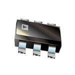
| 供应商器件封装 | SC-70-6 |
| 其它名称 | AD5602YKSZ-1500RL7DKR |
| 分辨率 | 8 bit |
| 包装 | Digi-Reel® |
| 商标 | Analog Devices |
| 安装类型 | 表面贴装 |
| 安装风格 | SMD/SMT |
| 封装 | Reel |
| 封装/外壳 | 6-TSSOP,SC-88,SOT-363 |
| 封装/箱体 | SC-70-6 |
| 工作温度 | -40°C ~ 125°C |
| 工厂包装数量 | 500 |
| 建立时间 | 6µs |
| 接口类型 | Serial |
| 数据接口 | I²C |
| 最大功率耗散 | 500 uW |
| 最大工作温度 | + 125 C |
| 最小工作温度 | - 40 C |
| 标准包装 | 1 |
| 电压参考 | External |
| 电压源 | 单电源 |
| 电源电压-最大 | 5.5 V |
| 电源电压-最小 | 2.7 V |
| 积分非线性 | +/- 0.5 LSB |
| 稳定时间 | 6 us |
| 系列 | AD5602 |
| 结构 | Resistor String |
| 转换器数 | 1 |
| 转换器数量 | 1 |
| 输出数和类型 | 1 电压,单极 |
| 输出类型 | Voltage |
| 采样比 | 1.7 MSPs |
| 采样率(每秒) | - |


- 商务部:美国ITC正式对集成电路等产品启动337调查
- 曝三星4nm工艺存在良率问题 高通将骁龙8 Gen1或转产台积电
- 太阳诱电将投资9.5亿元在常州建新厂生产MLCC 预计2023年完工
- 英特尔发布欧洲新工厂建设计划 深化IDM 2.0 战略
- 台积电先进制程称霸业界 有大客户加持明年业绩稳了
- 达到5530亿美元!SIA预计今年全球半导体销售额将创下新高
- 英特尔拟将自动驾驶子公司Mobileye上市 估值或超500亿美元
- 三星加码芯片和SET,合并消费电子和移动部门,撤换高东真等 CEO
- 三星电子宣布重大人事变动 还合并消费电子和移动部门
- 海关总署:前11个月进口集成电路产品价值2.52万亿元 增长14.8%


PDF Datasheet 数据手册内容提取
2.7 V to 5.5 V, <100 µA, 8-/10-/12-Bit nanoDACs with I2C Compatible Interface in LFCSP and SC70 Data Sheet AD5602/AD5612/AD5622 FEATURES FUNCTIONAL BLOCK DIAGRAM Single 8-, 10-, 12-bit DACs, 2 LSB INL VDD GND 6-lead LFCSP and SC70 packages Micropower operation: 100 µA maximum at 5 V POWER-ON AD5602/AD5612/AD5622 RESET Power down to <150 nA at 3 V 2.7 V to 5.5 V power supply REF(+) Guaranteed monotonic by design REGDIASCTER 8-/10D-/A1C2-BIT OBUUFTFPEURT VOUT Power-on reset to 0 V with brownout detection 3 power-down functions I2C compatible serial interface supports standard (100 kHz), INPUT POWER-DOWN fast (400 kHz), and high speed (3.4 MHz) modes COLNOTGRICOL CONTROLLOGIC NREETSWISOTORRK On-chip output buffer amplifier, rail-to-rail operation APrPoPceLsIsC cAonTtIrOolN S ADDR SCL SDA 05446-001 Data acquisition systems Figure 1. Portable battery-powered instruments Table 1. Related Devices Digital gain and offset adjustment Device No. Description Programmable voltage and current sources AD5601/AD5611/AD5621 2.7 V to 5.5 V, <100 µA, 8-, 10-, 12-bit Programmable attenuators nanoDAC with SPI interface in tiny LFCSP and SC70 packages GENERAL DESCRIPTION PRODUCT HIGHLIGHTS The AD5602/AD5612/AD5622, members of the nanoDAC® 1. Available in 6-lead LFCSP and SC70 packages. family, are single 8-, 10-, 12-bit buffered voltage-out digital-to- 2. Maximum 100 µA power consumption, single-supply analog converters (DAC) that operate from a single 2.7 V to operation. These devices operate from a single 2.7 V to 5.5 V 5.5 V supply, consuming <100 µA at 5 V. These DACs come in supply, typically consuming 0.2 mW at 3 V and 0.4 mW at tiny LFCSP and SC70 packages. Each DAC contains an on-chip 5 V, making them ideal for battery-powered applications. precision output amplifier that allows rail-to-rail output swing 3. The on-chip output buffer amplifier allows the output of to be achieved. the DAC to swing rail-to-rail with a typical slew rate of 0.5 V/µs. The AD5602/AD5612/AD5622 use a 2-wire I2C compatible 4. Reference derived from the power supply. serial interface that operates in standard (100 kHz), fast (400 kHz), 5. Standard, fast, and high speed mode I2C interface. and high speed (3.4 MHz) modes. 6. Designed for very low power consumption. The references for AD5602/AD5612/AD5622 derive from the 7. Power-down capability. When powered down, the DAC power supply inputs to give the widest dynamic output range. Each typically consumes <150 nA at 3 V. device incorporates a power-on reset circuit that ensures the DAC 8. Power-on reset and brownout detection. output powers up to 0 V and remains there until a valid write takes place to the device. The devices contain a power-down feature that reduces the current consumption of the devices to <150 nA at 3 V and provides software selectable output loads while in power-down mode. The devices are put into power-down mode over the serial interface. The low power consumption of the AD5602/AD5612/ AD5622 in normal operation makes them ideally suited for use in portable, battery operated equipment. The typical power consumption is 0.4 mW at 5 V. Rev. E Document Feedback Information furnished by Analog Devices is believed to be accurate and reliable. However, no responsibility is assumed by Analog Devices for its use, nor for any infringements of patents or other One Technology Way, P.O. Box 9106, Norwood, MA 02062-9106, U.S.A. rights of third parties that may result from its use. Specifications subject to change without notice. No license is granted by implication or otherwise under any patent or patent rights of Analog Devices. Tel: 781.329.4700 ©2005–2018 Analog Devices, Inc. All rights reserved. Trademarks and registered trademarks are the property of their respective owners. Technical Support www.analog.com
AD5602/AD5612/AD5622 Data Sheet TABLE OF CONTENTS Features .............................................................................................. 1 Resistor String ............................................................................. 15 Applications ....................................................................................... 1 Output Amplifier ........................................................................ 15 Functional Block Diagram .............................................................. 1 Serial Interface ................................................................................ 16 General Description ......................................................................... 1 Input Register .............................................................................. 16 Product Highlights ........................................................................... 1 Power-On Reset .......................................................................... 17 Revision History ............................................................................... 2 Power-Down Modes .................................................................. 17 Specifications ..................................................................................... 3 Write Operation.......................................................................... 18 I2C Timing Specifications ............................................................ 4 Read Operation........................................................................... 19 Timing Diagram ........................................................................... 5 High Speed Mode ....................................................................... 20 Absolute Maximum Ratings ............................................................ 6 Applications Information .............................................................. 21 ESD Caution .................................................................................. 6 Choosing a Reference as Power Supply ................................... 21 Pin Configurations and Function Descriptions ........................... 7 Bipolar Operation....................................................................... 21 Typical Performance Characteristics ............................................. 8 Power Supply Bypassing and Grounding ................................ 21 Terminology .................................................................................... 14 Outline Dimensions ....................................................................... 22 Theory of Operation ...................................................................... 15 Ordering Guide .......................................................................... 23 D/A Section ................................................................................. 15 REVISION HISTORY 6/2018—Rev. D to Rev. E 3/2006—Rev. A to Rev. B Changes to Features Section............................................................ 1 Changes to Table 2 ............................................................................. 3 Changes to Serial Interface Section .............................................. 16 Updates to Outline Dimensions ................................................... 22 Updated Outline Dimensions ....................................................... 22 Changes to Ordering Guide .......................................................... 23 Changes to Ordering Guide .......................................................... 23 Deleted Automotive Products Section ......................................... 23 8/2005—Rev. 0 to Rev. A Changes to Ordering Guide .......................................................... 22 10/2015—Rev. C to Rev. D Changes to Table 4 ............................................................................ 6 6/2005—Revision 0: Initial Version Changes to Read Operation Section ............................................ 19 Changes to Ordering Guide .......................................................... 23 5/2012—Rev. B to Rev. C Added 6-lead LFCSP Package ........................................... Universal Changes to Product Title ................................................................. 1 Changes to Ordering Guide .......................................................... 23 Rev. E | Page 2 of 23
Data Sheet AD5602/AD5612/AD5622 SPECIFICATIONS V = 2.7 V to 5.5 V, R = 2 kΩ to GND, C = 200 pF to GND; all specifications T to T , unless otherwise noted. DD L L MIN MAX Table 2. A, B, W, Y Versions1 Parameter Min Typ Max Unit Test Conditions/Comments STATIC PERFORMANCE DAC output unloaded Resolution Bits AD5602 8 AD5612 10 AD5622 12 Relative Accuracy2 AD5602 ±0.5 LSB B, Y versions AD5612 ±0.5 LSB B, Y versions ±4 LSB A version AD5622 ±2 LSB B, Y versions ±6 LSB A, W versions Differential Nonlinearity2 ±1 LSB Guaranteed monotonic by design Zero Code Error 0.5 10 mV All 0s loaded to DAC register Offset Error ±0.063 ±10 mV Full-Scale Error 0.5 mV All 1s loaded to DAC register Gain Error ±0.0004 ±0.037 % of FSR Zero Code Error Drift 5 µV/°C Gain Temperature Coefficient 2 ppm of FSR/°C OUTPUT CHARACTERISTICS3 Output Voltage Range 0 V V DD Output Voltage Settling Time 6 10 µs Code ¼ to ¾ Slew Rate 0.5 V/µs Capacitive Load Stability 470 pF R = ∞ L 1000 pF R = 2 kΩ L Output Noise Spectral Density 120 nV/Hz DAC code = midscale, 10 kHz Noise 2 DAC code = midscale, 0.1 Hz to 10 Hz bandwidth Digital-to-Analog Glitch Impulse 5 nV-sec 1 LSB change around major carry Digital Feedthrough 0.2 nV-sec DC Output Impedance 0.5 Ω Short Circuit Current 15 mA V = 3 V/5 V DD LOGIC INPUTS (SDA, SCL) I , Input Current ±1 µA IN V , Input Low Voltage 0.3 × V V INL DD V , Input High Voltage 0.7 × V V INH DD C , Pin Capacitance 2 pF IN V , Input Hysteresis 0.1 × V V HYST DD LOGIC OUTPUTS (OPEN DRAIN) V , Output Low Voltage 0.4 V I = 3 mA OL SINK 0.6 V I = 6 mA SINK Floating State Leakage Current ±1 µA Floating State Output Capacitance 2 pF Rev. E | Page 3 of 23
AD5602/AD5612/AD5622 Data Sheet A, B, W, Y Versions1 Parameter Min Typ Max Unit Test Conditions/Comments POWER REQUIREMENTS V 2.7 5.5 V DD I (Normal Mode) DAC active and excluding load current DD V = 4.5 V to 5.5 V 75 100 µA V = V and V = GND DD IH DD IL V = 2.7 V to 3.6 V 60 90 µA V = V and V = GND DD IH DD IL I (All Power-Down Modes) DD V = 4.5 V to 5.5 V 0.3 1 µA V = V and V = GND DD IH DD IL V = 2.7 V to 3.6 V 0.15 1 µA V = V and V = GND DD IH DD IL POWER EFFICIENCY I /I 96 % I = 2 mA, V = 5 V OUT DD LOAD DD 1 Temperature ranges for A, B versions: −40°C to +125°C, typical at 25°C. 2 Linearity calculated using a reduced code range 64 to 4032. 3 Guaranteed by design and characterization, not production tested. I2C TIMING SPECIFICATIONS V = 2.7 V to 5.5 V; all specifications T to T , f = 3.4 MHz, unless otherwise noted.1 DD MIN MAX SCL Table 3. Limit at T , MIN T MAX Parameter Test Conditions/Comments2 Min Max Unit Description f 3 Standard mode 100 KHz Serial clock frequency SCL Fast mode 400 KHz High speed mode, C = 100 pF 3.4 MHz B High speed mode, C = 400 pF 1.7 MHz B t Standard mode 4 µs t , SCL high time 1 HIGH Fast mode 0.6 µs High speed mode, C = 100 pF 60 ns B High speed mode, C = 400 pF 120 ns B t Standard mode 4.7 µs t , SCL low time 2 LOW Fast mode 1.3 µs High speed mode, C = 100 pF 160 ns B High speed mode, C = 400 pF 320 ns B t Standard mode 250 ns t , data setup time 3 SU;DAT Fast mode 100 ns High speed mode 10 ns t Standard mode 0 3.45 µs t , data hold time 4 HD;DAT Fast mode 0 0.9 µs High speed mode, C = 100 pF 0 70 ns B High speed mode, C = 400 pF 0 150 ns B t Standard mode 4.7 µs t , setup time for a repeated start condition 5 SU;STA Fast mode 0.6 µs High speed mode 160 ns t Standard mode 4 µs t , hold time (repeated) start condition 6 HD;STA Fast mode 0.6 µs High speed mode 160 ns t Standard mode 4.7 µs t , bus free time between a stop and a start condition 7 BUF Fast mode 1.3 µs Rev. E | Page 4 of 23
Data Sheet AD5602/AD5612/AD5622 Limit at T , MIN T MAX Parameter Test Conditions/Comments2 Min Max Unit Description t Standard mode 4 µs t , setup time for a stop condition 8 SU;STO Fast mode 0.6 µs High speed mode 160 ns t Standard mode 1000 ns t , rise time of SDA signal 9 RDA Fast mode 300 ns High speed mode, C = 100 pF 10 80 ns B High speed mode, C = 400 pF 20 160 ns B t Standard mode 300 ns t , fall time of SDA signal 10 FDA Fast mode 300 ns High speed mode, C = 100 pF 10 80 ns B High speed mode, C = 400 pF 20 160 ns B t Standard mode 1000 ns t , rise time of SCL signal 11 RCL Fast mode 300 ns High speed mode, C = 100 pF 10 40 ns B High speed mode, C = 400 pF 20 80 ns B t Standard mode 1000 ns t , rise time of SCL signal after a repeated start 11A RCL1 condition and after an acknowledge bit Fast mode 300 ns High speed mode, C = 100 pF 10 80 ns B High speed mode, C = 400 pF 20 160 ns B t Standard mode 300 ns t , fall time of SCL signal 12 FCL Fast mode 300 ns High speed mode, C = 100 pF 10 40 ns B High speed mode, C = 400 pF 20 80 ns B t 4 Fast mode 0 50 ns Pulse width of spike suppressed SP High speed mode 0 10 ns 1 See Figure 2. High speed mode timing specification applies to the AD5602-1/AD5612-1/AD5622-1 only. Standard and fast mode timing specifications apply to the AD5602-1/AD5612-1/AD5622-1 and the AD5602-2/AD5612-2/AD5622-2. 2 CB refers to the capacitance on the bus line. 3 The SDA and SCL timing is measured with the input filters enabled. Switching off the input filters improves the transfer rate but has a negative effect on EMC behavior of the device. 4 Input filtering on the SCL and SDA inputs suppress noise spikes that are less than 50 ns for fast mode or 10 ns for high speed mode. TIMING DIAGRAM t11 t12 t6 t2 SCL t6 t1 t5 t8 t4 t3 t10 t9 SDA P t7 S S P 05446-002 Figure 2. 2-Wire Serial Interface Timing Diagram Rev. E | Page 5 of 23
AD5602/AD5612/AD5622 Data Sheet ABSOLUTE MAXIMUM RATINGS T = 25°C, unless otherwise noted. A Stresses at or above those listed under Absolute Maximum Ratings may cause permanent damage to the product. This is a Table 4. stress rating only; functional operation of the product at these Parameter Rating or any other conditions above those indicated in the operational V to GND –0.3 V to + 7.0 V DD section of this specification is not implied. Operation beyond Digital Input Voltage to GND –0.3 V to V + 0.3 V DD the maximum operating conditions for extended periods may V to GND –0.3 V to V + 0.3 V OUT DD affect product reliability. Operating Temperature Range −40°C to +125°C Storage Temperature Range –65°C to +160°C ESD CAUTION Maximum Junction Temperature 150°C SC70 Package θ Thermal Impedance 332°C/W JA θ Thermal Impedance 120°C/W JC LFCSP Package θ Thermal Impedance 95°C/W JA Lead Temperature, Soldering Vapor Phase (60 sec) 215°C Infrared (15 sec) 220°C ESD 2.0 kV Rev. E | Page 6 of 23
Data Sheet AD5602/AD5612/AD5622 PIN CONFIGURATIONS AND FUNCTION DESCRIPTIONS ADDR 1 AD5602/ 6 VOUT ADDR 1 AD5602/ 6 SDA AD5612/ AD5612/ SCL 2 AD5622 5 GND GND 2 AD5622 5 SCL SDA 3 (NToOtPtoVSIEcaWle) 4 VDD 05446-003 VOUT 3 (NToOt Pto V SIEcWale) 4 VDD N1.O TTTOHEE SG ERXOPUONSDE (DG PNADD). SHOULD BE CONNECTED 05446-051 Figure 3. SC70 Pin Configuration Figure 4. LFCSP Pin Configuration Table 5. SC70 Pin Function Descriptions Table 6. LFCSP Pin Function Descriptions Pin No. Mnemonic Description Pin No. Mnemonic Description 1 ADDR Three-State Address Input. Sets the 1 ADDR Three-State Address Input. Sets the two least significant bits (Bit A1, Bit A0) two least significant bits (Bit A1, Bit A0) of the 7-bit slave address (see Table 7). of the 7-bit slave address (see Table 7). 2 SCL Serial Clock Line. This is used in 2 GND Ground. The ground reference point for conjunction with the SDA line to clock all circuitry on the device. data into or out of the 16-bit input 3 V Analog Output Voltage from the DAC. register. OUT The output amplifier has rail-to-rail 3 SDA Serial Data Line. This is used in operation. conjunction with the SCL line to clock 4 V Power Supply Input. These devices can data into or out of the 16-bit input DD be operated from 2.7 V to 5.5 V, and V register. It is a bidirectional, open-drain DD are decoupled to GND. data line that is pulled to the supply with an external pull-up resistor. 5 SCL Serial Clock Line. This is used in conjunction with the SDA line to clock 4 V Power Supply Input. These devices can DD data into or out of the 16-bit input be operated from 2.7 V to 5.5 V, and V DD register. are decoupled to GND. 6 SDA Serial Data Line. This is used in 5 GND Ground. The ground reference point for conjunction with the SCL line to clock all circuitry on the devices. data into or out of the 16-bit input 6 V Analog Output Voltage from the DAC. OUT register. It is a bidirectional, open-drain The output amplifier has rail-to-rail data line that are pulled to the supply operation. with an external pull-up resistor. EPAD Exposed Pad. The exposed pad is connected to ground (GND). Rev. E | Page 7 of 23
AD5602/AD5612/AD5622 Data Sheet TYPICAL PERFORMANCE CHARACTERISTICS 1.0 0.05 VDD=5V VDD=5V 0.8 TA=25°C 0.04 TA=25°C 0.6 0.03 0.4 0.02 B) B) R (LS 0.2 R (LS 0.01 RO 0 RO 0 R R NL E –0.2 NL E–0.01 I D –0.4 –0.02 –0.6 –0.03 –0.8 –0.04 –1.00 500 1000 1500DA2C00C0ODE2500 3000 3500 4000 05446-004 –0.050 200 400DACCOD6E00 800 1000 05446-048 Figure 5. Typical AD5622 Integral Nonlinearity Error Figure 8. Typical AD5612 Differential Nonlinearity Error 0.15 0.06 0.10 VTADD==255°VC VTADD==255°VC 0.04 0.05 SB) B) 0.02 L S OR ( 0 R (L R O 0 R R E–0.05 R NL L E D N –0.10 I–0.02 –0.15 –0.04 –0.200 500 1000 1500DA2C00C0ODE2500 3000 3500 4000 05446-005 –0.060 50 100DACCOD1E50 200 250 05446-049 Figure 6. Typical AD5622 Differential Nonlinearity Error Figure 9. Typical AD5602 Integral Nonlinearity Error 0.25 0.015 VDD=5V VDD=5V 0.20 TA=25°C TA=25°C 0.010 0.15 0.10 B) B)0.005 LS 0.05 LS R ( R ( RO 0 RO 0 R R NL E–0.05 NL E I–0.10 D–0.005 –0.15 –0.010 –0.20 –0.250 200 400DACCOD6E00 800 1000 05446-047 –0.0150 50 100DACCOD1E50 200 250 05446-050 Figure 7. Typical AD5612 Integral Nonlinearity Error Figure 10. Typical AD5602 Differential Nonlinearity Error Rev. E | Page 8 of 23
Data Sheet AD5602/AD5612/AD5622 1 0.5 VDD=5V TA=25°C 0 TA=25°C 0.4 –1 0.3 B) MAXDNL SB) –2 R (LS 0.2 L O TUE ( ––43 NL ERR 0.10 D –5 –0.1 MINDNL –6 –0.2 –70 500 1000 1500DA2C00C0ODE2500 3000 3500 4000 05446-006 –0.32.7 3.2 3.7 VDD4(V.2) 4.7 5.2 05446-009 Figure 11. Typical AD5622 Total Unadjusted Error Figure 14. AD5622 DNL Error vs. Supply 0.8 0.5 TA=25°C MAX INL 0.6 0.4 MAX INL=5V 0.4 0.3 MAX INL=3V B) B) S 0.2 S 0.2 L L R ( R ( RO 0 RO 0.1 R R E E NL –0.2 NL 0 I I –0.4 –0.1 –0.6 MIN INL –0.2 MIN INL=5V MIN INL=3V –0.82.7 3.2 3.7 VDD4(V.2) 4.7 5.2 05446-007 –0.3–40 –20 0 T2E0MPER4A0TURE60(°C) 80 100 120 05446-010 Figure 12. AD5622 INL Error vs. Supply Figure 15. AD5622 INL Error vs. Temperature (3 V/5 V Supply) 0 8 TA=25°C –1 MAXTUE 7 MAXTUE=5V –2 6 TUE (LSB) ––43 TUE (LSB) 54 MAXTUE=3V –5 3 MINTUE=5V –6 MINTUE 2 –7 1 MINTUE=3V –82.7 3.2 3.7 VDD4(V.2) 4.7 5.2 05446-008 0–40 –20 0 T2E0MPER4A0TURE60(°C) 80 100 120 05446-011 Figure 13. AD5622 Total Unadjusted Error vs. Supply Figure 16. AD5622 Total Unadjusted Error vs. Temperature (3 V/5 V Supply) Rev. E | Page 9 of 23
AD5602/AD5612/AD5622 Data Sheet 0.6 1.8 0.5 1.6 OFFSETERROR=3V 0.4 1.4 MAXDNL=5V B) 0.3 1.2 LS V) OR ( 0.2 MAXDNL=3V R (m1.0 R O L ER 0.1 ERR0.8 N D 0 0.6 OFFSETERROR=5V –0.1 MINDNL=5V 0.4 –0.2 0.2 MINDNL=3V –0.3–40 –20 0 T2E0MPER4A0TURE60(°C) 80 100 120 05446-012 0–40 –20 0 T2E0MPER4A0TURE60(°C) 80 100 120 05446-015 Figure 17. AD5622 DNL Error vs. Temperature (3 V/5 V Supply) Figure 20. Offset Error vs. Temperature (3 V/5 V Supply) 4 0.00025 GAINERROR=3V 2 ZEROCODEERROR=3V 0.00020 ZEROCODEERROR=5V 0 V) SR)0.00015 m –2 F RROR ( –4 ROR (% GAINERROR=5V E FULL-SCALEERROR=3V ER0.00010 –6 0.00005 –8 FULL-SCALEERROR=5V –10–40 –20 0 T2E0MPER4A0TURE6(0°C) 80 100 120 05446-013 0–40 –20 0 T2E0MPER4A0TURE60(°C) 80 100 120 05446-016 Figure 18. Zero Code/Full-Scale Error vs. Temperature (3 V/5 V Supply) Figure 21. Gain Error vs. Temperature (3 V/5 V Supply) 1 0.10 TA=25°C 0 ZEROCODEERROR 0.09 TA=25°C 0.08 –1 0.07 –2 V) 0.06 OR (m –3 (µA)D0.05 ERR –4 ID0.04 –5 0.03 –6 0.02 FULL-SCALEERROR –7 0.01 –82.7 3.2 3.7 VDD4(V.2) 4.7 5.2 05446-014 02.7 3.2 3.7 VDD4(V.2) 4.7 5.2 05446-017 Figure 19. Zero Code/Full-Scale Error vs. Supply Voltage Figure 22. Supply Current vs. Supply Voltage Rev. E | Page 10 of 23
Data Sheet AD5602/AD5612/AD5622 12 VDD=3V VDD=5V 0.10 VIH =VDD VIH =VDD VIL= GND VIL= GND 0.09 10 TA=25°C TA=25°C 0.08 8 Y 0.07 C VDD=5V EN 0.06 U 6 A) EQ I(µDD00..0045 VDD=3V FR 4 0.03 2 0.02 0.01 0 67 9 1 2 4 5803570247914 52 9 7 4 1 8417396284073 45 5 6 7 8 8677889001223 0–40 –20 0 20TEMP4E0RATU6R0E(°C8)0 100 120 140 05446-018 0.050.05 0.05 0.05 0.05 0.05 IDD0.05(µ0.06A)0.060.060.060.060.060.070.070.070.070.070.07 05446-021 Figure 23. Supply Current vs. Temperature (3 V/5 V Supply) Figure 26. IDD Histogram (3 V/5 V Supply) 70 0.8 60 VDD=5V TA=25°C 0.6 VTADD==255°VC DACLOADEDWITHZERO-SCALECODE 50 0.4 VDD=3V A)40 V) 0.2 I (µDD30 ΔV (O 0.0 20 –0.2 DACLOADEDWITHFULL-SCALECODE 10 –0.4 00 2000 4000 6000DA8C00C0OD1E0000 12000 14000 16000 05446-019 –0.6 –15 –10 –5 I(m0A) 5 10 15 05446-037 Figure 24. Supply Current vs. Digital Input Code Figure 27. Sink and Source Capability 900 800 VSCDDL/=SD5VA INCREASING VTADD==255°VC VDD 700 600 SCL/SDADECREASING VDD=5V A) 500 µ CH1 (D SCL/SDA ID 400 INCREASING VDD=3V SCL/SDADECREASING VOUT=70mV 300 VDD=3V 200 100 00 0.5 1.0 1.5 2.0VLO2G.I5C(V)3.0 3.5 4.0 4.5 5.0 05446-020 CH2 CH1=1V/DIV,CH2=20mV/DIV,TIMEBASE=20µs/DIV 05446-038 Figure 25. Supply Current vs. SCL/SDA Logic Voltage Figure 28. Power On Reset to 0 V Rev. E | Page 11 of 23
AD5602/AD5612/AD5622 Data Sheet CH1 VDD VDD=5V TA=25°C VDD=5V CH1 TA=25°C CH2 CH2 VOUT CH1=5V/DIV,CH2=1V/DIV,TIMEBASE=2µs/DIV 05446-039 CH1=1V/DIV,CH2=3V/DIV,TIMEBASE=50µs/DIV 05446-042 Figure 29. Exiting Power-Down Mode Figure 32. VOUT vs. VDD 2.458 2.456 VDD=5V 2.454 CH1 TA=25°C 2.452 (V)2.450 E UD2.448 T PLI2.446 M A2.444 2.442 VDD=5V 2.440 TA=25°C LOAD=2kΩAND220pF 2.438 CODE0x800TO0x7FF CH2 CH1=5V/DIV,CH2=1V/DIV,TIMEBASE=2µs/DIV 05446-040 2.4360 100 S2A0M0PLENUM30B100EnRs/SAMP4L0E0NUMBER500 05446-043 Figure 30. Full-Scale Settling Time Figure 33. DAC Glitch Impulse 2.4278 VDD=5V 2.4276 TA=25°C LOAD=2kΩAND220pF VDD=5V 10ns/SAMPLENUMBER CH1 TA=25°C 2.4274 2.4272 V) DE ( 2.4270 U T LI 2.4268 P M A 2.4266 CH2 2.4264 2.4262 CH1=5V/DIV,CH2=1V/DIV,TIMEBASE=2µs/DIV 05446-041 2.42600 100 S2A00MPLENUM3B00ER 400 500 05446-044 Figure 31. Half Scale Settling Time Figure 34. Digital Feedthrough Rev. E | Page 12 of 23
Data Sheet AD5602/AD5612/AD5622 700 VTADD==255°VC Hz) VTADD==255°VC MIDSCALELOADED V/600 UNLOADED OUTPUT n ( Y SIT500 N E D L400 CH1 RA T ZEROSCALE C E300 P S E NOIS200 MIDSCALE FULLSCALE T PU100 T Figure 35. 1/f NoisCeH, 10.=1 5HµzV /tDoI V10 Hz Bandwidth 05446-045 OU 0100 1000FREQUENCY(Hz1)0000 100000 05446-046 Figure 36. Output Noise Spectral Density Rev. E | Page 13 of 23
AD5602/AD5612/AD5622 Data Sheet TERMINOLOGY Relative Accuracy Gain Error For the DAC, relative accuracy or integral nonlinearity (INL) is Gain error is a measure of the span error of the DAC. It is the a measure of the maximum deviation, in least significant bits deviation in slope of the DAC transfer characteristic from ideal (LSB), from a straight line passing through the endpoints of the expressed as a percent of the full-scale range. DAC transfer function. A typical INL vs. code plot can be seen Total Unadjusted Error (TUE) in Figure 5. Total unadjusted error is a measure of the output error taking Differential Nonlinearity (DNL) all the various errors into account. A typical TUE vs. code plot Differential nonlinearity is the difference between the measured can be seen in Figure 11. change and the ideal 1 LSB change between any two adjacent codes. Zero Code Error Drift A specified differential nonlinearity of ±1 LSB maximum ensures Zero code error drift is a measure of the change in zero code monotonicity. This DAC is guaranteed monotonic by design. A error with a change in temperature. It is expressed in µV/°C. typical DNL vs. code plot can be seen in Figure 6. Gain Error Drift Zero Code Error Gain error drift is a measure of the change in gain error with Zero code error is due to a combination of the offset errors in changes in temperature. It is expressed in (ppm of full-scale the DAC and output amplifier; it is a measure of the output error range)/°C. when zero code (0x0000) is loaded to the DAC register. Ideally, Digital-to-Analog Glitch Impulse the output is 0 V. The zero code error is always positive in the Digital-to-analog glitch impulse is the impulse injected into the AD5602/AD5612/AD5622 because the output of the DAC cannot analog output when the input code in the DAC register changes go below 0 V. Zero code error is expressed in mV. A plot of zero state. It is normally specified as the area of the glitch in nV-sec code error vs. temperature can be seen in Figure 18. and is measured when the digital input code is changed by 1 LSB at Full-Scale Error the major carry transition (0x7FFF to 0x8000) (see Figure 33). Full-scale error is a measure of the output error when full-scale Digital Feedthrough code (0xFFFF) is loaded to the DAC register; it is expressed in Digital feedthrough is a measure of the impulse injected into the percent of full-scale range. Ideally, the output is V – 1 LSB. A DD analog output of the DAC from the digital inputs of the DAC, but is plot of full-scale error vs. temperature can be seen in Figure 18. measured when the DAC output is not updated. It is specified in nV-sec and measured with a full-scale code change on the data bus, that is, from all 0s to all 1s, and vice versa (see Figure 34). Rev. E | Page 14 of 23
Data Sheet AD5602/AD5612/AD5622 THEORY OF OPERATION D/A SECTION The AD5602/AD5612/AD5622 DACs are fabricated on a R CMOS process. The architecture consists of a string DACs followed by an output buffer amplifier. Figure 37 shows a block R diagram of the DAC architecture. VDD R TO OUTPUT AMPLIFIER REF(+) DACREGISTER NREETSWISOTORRK VOUT REF(–) OUTPUT GND AMPLIFIER 05446-022 Figure 37. DAC Architecture R Since the input coding to the DAC is straight binary, the ideal output voltage is given by R VOUT =VDD×2Dn 05446-023 Figure 38. Resistor String Structure where: OUTPUT AMPLIFIER D is the decimal equivalent of the binary code that is loaded to the DAC register; it can range from 0 to 255 (AD5602), 0 to 1023 The output buffer amplifier is capable of generating rail-to-rail (AD5612), or 0 to 4095 (AD5622). voltages on its output, giving an output range of 0 V to V . It is DD n is the bit resolution of the DAC. capable of driving a load of 2 kΩ in parallel with 1000 pF to GND. RESISTOR STRING The source and sink capabilities of the output amplifier can be seen in Figure 27. The slew rate is 0.5 V/µs with a half scale settling The resistor string structure is shown in Figure 38. It is simply a time of 5 µs with the output unloaded. string of resistors, each of value R. The code loaded to the DAC register determines at which node on the string the voltage is tapped off to be fed into the output amplifier. The voltage is tapped off by closing one of the switches connecting the string to the amplifier. Because it is a string of resistors, it is guaranteed monotonic. Rev. E | Page 15 of 23
AD5602/AD5612/AD5622 Data Sheet SERIAL INTERFACE The AD5602/AD5612/AD5622 have 2-wire I2C compatible 3. When all data bits have been read or written, a stop serial interfaces (refer to I2C-Bus Specification, Version 2.1, condition is established. In write mode, the master pulls January 2000, available from Philips Semiconductor). The the SDA line high during the 10th clock pulse to establish a AD5602/AD5612/AD5622 can be connected to an I2C bus as a stop condition. If a stop condition is generated between the slave device, under the control of a master device. See Figure 2 7th and 8th clock pulse of the I2C address frame, a power cycle for a timing diagram of a typical write sequence. is required to recover the device. In read mode, the master issues a no acknowledge for the ninth clock pulse (that is, The AD5602/AD5612/AD5622 support standard (100 kHz), the SDA line remains high). The master then brings the fast (400 kHz), and high speed (3.4 MHz) data transfer modes. SDA line low before the 10th clock pulse, and then high Support is not provided for 10-bit addressing and general call during the 10th clock pulse to establish a stop condition. addressing. The AD5602/AD5612/AD5622 each have a 7-bit slave address. Table 7. Device Address Selection The five most significant bits (MSB) are 00011 and the two LSBs ADDR A1 A0 are determined by the state of the ADDR pin. The facility to GND 1 1 make hardwired changes to ADDR allows the user to incorporate V 0 0 DD up to three of these devices on one bus as outlined in Table 7. NC (No Connection) 1 0 The 2-wire serial bus protocol operates as follows: INPUT REGISTER 1. The master initiates data transfer by establishing a start condition, which is when a high to low transition on the The input register is 16 bits wide. Figure 39, Figure 40, and SDA line occurs while SCL is high. The following byte is Figure 41 illustrate the contents of the input register for each the address byte, which consists of the 7-bit slave address. device. Data is loaded into the device as a 16-bit word under the The slave address corresponding to the transmitted address control of an SCL input. The timing diagram for this operation responds by pulling SDA low during the ninth clock pulse is shown in Figure 2. The 16-bit word consists of four control (this is termed the acknowledge bit). At this stage, all other bits followed by 8, 10, or 12 bits of data, depending on the device devices on the bus remain idle while the selected device type. MSB (DB15) is loaded first. The first two bits are reserved waits for data to be written to, or read from, its shift register. bits that must be set to zero; the next two bits are control bits 2. Data is transmitted over the serial bus in sequences of nine that select the mode of operation of the device (normal mode or clock pulses (eight data bits followed by an acknowledge any one of three power-down modes). See the Power-Down bit). The transitions on the SDA line must occur during the Modes section for a complete description. The remaining bits low period of SCL and remain stable during the high are left justified DAC data bits, starting with the MSB and period of SCL. ending with the LSB. DB15(MSB) DB0(LSB) 0 0 PD1 PD0 D7 D6 D5 D4 D3 D2 D1 D0 X X X X DATABITS 05446-024 Figure 39. AD5602 Input Register Contents DB15(MSB) DB0(LSB) 0 0 PD1 PD0 D9 D8 D7 D6 D5 D4 D3 D2 D1 D0 X X DATABITS 05446-025 Figure 40. AD5612 Input Register Contents DB15(MSB) DB0(LSB) 0 0 PD1 PD0 D11 D10 D9 D8 D7 D6 D5 D4 D3 D2 D1 D0 DATABITS 05446-026 Figure 41. AD5622 Input Register Contents Rev. E | Page 16 of 23
Data Sheet AD5602/AD5612/AD5622 POWER-ON RESET When both bits are set to 0, the device works normally with its usual power consumption of 100 µA maximum at 5 V. However, The AD5602/AD5612/AD5622 each contain a power-on reset for the three power-down modes, the supply current falls to circuit that controls the output voltage during power-up. The <150 nA (at 3 V). Not only does the supply current fall, but the DAC register is filled with zeros and the output voltage is 0 V output stage is internally switched from the output of the amplifier where it remains until a valid write sequence is made to the to a resistor network of known values. This gives the advantage DAC. This is useful in applications in which it is important to of knowing the output impedance of the device while the device know the state of the DAC output while it is in the process of is in power-down mode. There are three different options. The powering up. output is connected internally to GND through a 1 kΩ resistor, POWER-DOWN MODES a 100 kΩ resistor, or it is left open circuited (three-state). Figure 42 The AD5602/AD5612/AD5622 each contain four separate shows the output stage. modes of operation. These modes are software programmable by setting Bit PD1 and Bit PD0 in the control register. Table 8 shows how the state of the bits corresponds to the mode of SRTERSINISGTDOARC AMPLIFIER VOUT operation of the device. Table 8. Modes of Operation POWER-DOWN PD1 PD0 Operating Mode CIRCUITRY RESISTOR 00 01 NPoowrmera-ld oopwenra (t1io knΩ load to GND) NETWORK 05446-027 Figure 42. Output Stage During Power-Down 1 0 Power-down (100 kΩ load to GND) 1 1 Power-down (Three-state output) The bias generator, output amplifier, resistor string, and other associated linear circuitry are all shut down when the power- down mode is activated. However, the contents of the DAC register are unaffected when in power-down. The time to exit power-down is typically 14 µs for V = 5 V and 17 µs for V = DD DD 3 V (see Figure 29). Rev. E | Page 17 of 23
AD5602/AD5612/AD5622 Data Sheet WRITE OPERATION Two bytes of data are then written to the DAC, the most significant byte followed by the least significant byte as shown in When writing to the AD5602/AD5612/AD5622, the user must Figure 40; both of these data bytes are acknowledged by the begin with a start command followed by an address byte (R/W = AD5602/AD5612/AD5622. A stop condition follows. The write 0), after which the DAC acknowledges that it is prepared to operations for the three DACs are shown in Figure 43, Figure 44, receive data by pulling SDA low. and Figure 45. 1 9 1 9 SCL SDA 0 0 0 1 1 A1 A0 R/W 0 0 PD1 PD0 D7 D6 D5 D4 STARTBY ACK.BY ACK.BY MASTER AD5602 AD5602 FRAME1 FRAME2 SERIALBUSADDRESSBYTE MOSTSIGNIFICANTDATABYTE 9 1 9 SCL(CONTINUED) SDA(CONTINUED) D3 D2 D1 D0 X X X X ACK.BY STOPBY LEASTSIGNFIFRIACMAENT3DATABYTE AD5602 MASTER 05446-028 Figure 43. AD5602 Write Sequence 1 9 1 9 SCL SDA 0 0 0 1 1 A1 A0 R/W 0 0 PD1 PD0 D9 D8 D7 D6 STARTBY ACK.BY ACK.BY MASTER AD5612 AD5612 FRAME1 FRAME2 SERIALBUSADDRESSBYTE MOSTSIGNIFICANTDATABYTE 9 1 9 SCL(CONTINUED) SDA(CONTINUED) D5 D4 D3 D2 D1 D0 X X ACK.BY STOPBY LEASTSIGNFIFRIACMAENT3DATABYTE AD5612 MASTER 05446-029 Figure 44. AD5612 Write Sequence 1 9 1 9 SCL SDA 0 0 0 1 1 A1 A0 R/W 0 0 PD1 PD0 D11 D10 D9 D8 STARTBY ACK.BY ACK.BY MASTER AD5622 AD5622 FRAME1 FRAME2 SERIALBUSADDRESSBYTE MOSTSIGNIFICANTDATABYTE 9 1 9 SCL(CONTINUED) SDA(CONTINUED) D7 D6 D5 D4 D3 D2 D1 D0 ACK.BY STOPBY LEASTSIGNFIFRIACMAENT3DATABYTE AD5622 MASTER 05446-030 Figure 45. AD5622 Write Sequence Rev. E | Page 18 of 23
Data Sheet AD5602/AD5612/AD5622 READ OPERATION The DAC then shifts out two bytes of data, both acknowledged by the master as shown in Figure 46, Figure 47, and Figure 48. A When reading data back from the AD5602/AD5612/AD5622, stop condition follows. When a read operation is performed, the the user begins with a start command followed by an address DAC shifts out the last transferred command. If a second readback byte (R/W = 1), after which the DAC acknowledges that it is operation is executed, the device shifts out 0x00 prepared to transmit data by pulling SDA low. 1 9 1 9 SCL SDA 0 0 0 1 1 A1 A0 R/W PD1 PD0 D7 D6 D5 D4 D3 D2 STARTBY ACK.BY ACK.BY MASTER AD5602 MASTER FRAME1 FRAME2 SERIALBUSADDRESSBYTE MOSTSIGNIFICANTDATABYTEFROMAD5602 1 9 SCL(CONTINUED) SDA(CONTINUED) D1 D0 0 0 0 0 0 0 NOACK.BY STOPBY LEASTSIGNIFICANFTRDAAMTEA3BYTEFROMAD5602MASTER MASTER 05446-031 Figure 46. AD5602 Read Sequence 1 9 1 9 SCL SDA 0 0 0 1 1 A1 A0 R/W PD1 PD0 D9 D8 D7 D6 D5 D4 STARTBY ACK.BY ACK.BY MASTER AD5612 MASTER FRAME1 FRAME2 SERIALBUSADDRESSBYTE MOSTSIGNIFICANTDATABYTEFROMAD5612 1 9 SCL(CONTINUED) SDA(CONTINUED) D3 D2 D1 D0 0 0 0 0 NOACK.BY STOPBY LEASTSIGNIFICANFTRDAAMTEA3BYTEFROMAD5612MASTER MASTER 05446-032 Figure 47. AD5612 Read Sequence 1 9 1 9 SCL SDA 0 0 0 1 1 A1 A0 R/W PD1 PD0 D11 D10 D9 D8 D7 D6 STARTBY ACK.BY ACK.BY MASTER AD5622 MASTER FRAME1 FRAME2 SERIALBUSADDRESSBYTE MOSTSIGNIFICANTDATABYTEFROMAD5622 1 9 SCL(CONTINUED) SDA(CONTINUED) D5 D4 D3 D2 D1 D0 0 0 NOACK.BY STOPBY LEASTSIGNIFICANFTRDAAMTEA3BYTEFROMAD5622MASTER MASTER 05446-033 Figure 48. AD5622 Read Sequence Rev. E | Page 19 of 23
AD5602/AD5612/AD5622 Data Sheet HIGH SPEED MODE The master must then issue a repeated start followed by the device address. The selected device then acknowledges the High speed mode communication commences after the master address. All devices continue to operate in high speed mode addresses all devices connected to the bus with the Master until the master issues a stop condition. When the stop Code 00001XXX to indicate that a high speed mode transfer is condition is issued, the devices return to standard/fast mode. to begin. No device connected to the bus is permitted to acknowledge the high speed master code, therefore, the code is followed by a no acknowledge. FASTMODE HIGH-SPEEDMODE 1 9 1 9 SCL SDA 0 0 0 0 1 X X X 0 0 0 1 1 A1 A0 R/W STARTBY NACK. SR ACK.BY MASTER HS-MODEMASTERCODE SERIALBUSADDRESSBYTE AD56x2 05446-034 Figure 49. Placing the AD5602/AD5612/AD5622 into High Speed Mode Rev. E | Page 20 of 23
Data Sheet AD5602/AD5612/AD5622 APPLICATIONS INFORMATION CHOOSING A REFERENCE AS POWER SUPPLY With V = 5 V, R1 = R2 = 10 kΩ. DD The AD5602/AD5612/AD5622 come in tiny LFCSP and SC70 10×D V = −5V packages with less than 100 µA supply current, thereby making O 2n the choice of reference dependent upon the application This is an output voltage range of ±5 V with 0x000 corresponding requirement. For space-saving applications, the ADR425 is to a −5 V output, and 0xFFF corresponding to a +5 V output. available in an SC70 package with excellent drift at 3ppm/°C. It R2 also provides very good noise performance at 3.4 µV p-p in the 10kΩ 0.1 Hz to 10 Hz range. R1 +5V +5V 10kΩ Because the supply current required by the AD5602/AD5612/ AD5622 DACs is extremely low, they are ideal for low supply AODP822905/ ±5V OUT applications. The ADR293 voltage reference is recommended in VDD AD5602/ VOUT 10µF 0.1µF AD5612/ this case. This requires 15 µA of quiescent current and can AD5622 –5V therefor7eV drive multiple DACs in the one system, if required. SDASCL 05446-036 Figure 51. Bipolar Operation with the AD5602/AD5612/AD5622 5V ADR425 POWER SUPPLY BYPASSING AND GROUNDING When accuracy is important in a circuit, it is helpful to carefully AD5602/ VOUT=0VTO5V consider the power supply and ground return layout on the board. SCL AD5612/ The printed circuit board containing the AD5602/AD5612/ SDA AD5622 05446-035 AowDn5 6ar2e2a h oafs t sheep baoraatred a. nIfa tlhogeA anDd5 6d0ig2i,t aAl Dse5c6t1io2n, so,r e AacDh5 h6a2v2i nisg i ints Figure 50. ADR425 as Power Supply a system in which other devices require an AGND to DGND Examples of some recommended precision references for use as connection, the connection is made at one point only. This ground supplies to the AD5602/AD5612/AD5622 are shown in Table 9. point must be as close as possible to the AD5602/AD5612/ AD5622. Table 9. Recommended Precision References The power supply to the AD5602/AD5612/AD5622 is bypassed Initial Temperature Device Accuracy Drift 0.1 Hz to 10 Hz Noise with 10 µF and 0.1 µF capacitors. The capacitors must be No. (mV max) (ppm/°C max) (µV p-p typ) physically as close as possible to the device with the 0.1 µF ADR435 ±6 3 3.4 capacitor ideally right up against the device. The 10 µF ADR425 ±6 3 3.4 capacitors are the tantalum bead type. It is important that the ADR02 ±5 3 15 0.1 µF capacitor has low effective series resistance (ESR) and ADR395 ±6 25 5 effective series inductance (ESI), such as common ceramic types. This 0.1 µF capacitor provides a low impedance path to ground BIPOLAR OPERATION for high frequencies caused by transient currents due to internal logic switching. The AD5602/AD5612/AD5622 are designed for single-supply operation, but a bipolar output range is also possible using the The power supply line has as large a trace as possible to provide circuit in Figure 51. The circuit in Figure 51 gives an output a low impedance path and reduce glitch effects on the supply voltage range of ±5 V. Rail-to-rail operation at the amplifier output line. Clocks and other fast switching digital signals must be is achievable using an AD820 or an OP295 as the output amplifier. shielded from other devices of the board by digital ground. Avoid crossover of digital and analog signals if possible. When The output voltage for any input code can be calculated as traces cross on opposite sides of the board, ensure they run at D R1+R2 R2 right angles to each other to reduce feedthrough effects through the VO =VDD×2n× R1 −VDD×R1 board. The best board layout technique is the microstrip technique where the component side of the board is dedicated where: to the ground plane only and the signal traces are placed on the D represents the input code in decimal. solder side. However, the microstrip technique is not always n represents the bit resolution of the DAC. possible with a 2-layer board. Rev. E | Page 21 of 23
AD5602/AD5612/AD5622 Data Sheet OUTLINE DIMENSIONS 2.20 2.00 1.80 1.35 6 5 4 2.40 1.25 2.10 1.15 1 2 3 1.80 0.65BSC 1.30BSC 1.00 1.10 0.40 0.90 0.80 0.10 0.70 0.46 0.10MAX 0.30 SPELAATNIENG 00..2028 0.36 COPLANARITY 0.15 0.26 0.10 COMPLIANTTOJEDECSTANDARDSMO-203-AB 072809-A Figure 52. 6-Lead Thin Shrink Small Outline Transistor Package [SC70] (KS-6) Dimensions shown in millimeters DETAIL A (JEDEC 95) 1.50 2.10 1.40 2.00 1.30 1.90 0.65 REF 4 6 0.20 MIN 3.10 EXPOSED 1.70 3.00 PAD 1.60 PIN 1 INDEX 2.90 0.45 1.50 AREA 0.40 0.35 3 1 TOP VIEW BOTTOM VIEW PININD I1CATOR AREA OPTIONS (SEE DETAIL A) FOR PROPER CONNECTION OF 000...877050 0.203 REF 00..0050 MMAINX TTFHHUENE CPETIXNIPO CONOS DNEEDFSI GPCAURDRIP,A TRTIOEIOFNNES RA NTOD SECTION OF THIS DATA SHEET. SEATING 0.35 COPLANARITY PLANE 0.30 0.08 PKG-003859 0.25 COMPLIANTTOJEDEC STANDARDS MO-229 01-26-2017-B Figure 53. 6-Lead Lead Frame Chip Scale Package [LFCSP] 2.00 mm × 3.00 mm Body and 0.75 mm Package Height (CP-6-5) Dimensions shown in millimeters Rev. E | Page 22 of 23
Data Sheet AD5602/AD5612/AD5622 ORDERING GUIDE I2C Interface Modes Temperature Power Supply Package Package Marking Model1 INL (max) Supported Range Range Description Option Code AD5602YKSZ-1500RL7 ±0.5 LSB Standard, fast and −40°C to +125°C 2.7 V to 5.5 V 6-Lead SC70 KS-6 D5W high speed AD5602YKSZ-1REEL7 ±0.5 LSB Standard, fast and −40°C to +125°C 2.7 V to 5.5 V 6-Lead SC70 KS-6 D5W high speed AD5602BKSZ-2500RL7 ±0.5 LSB Standard, fast −40°C to +125°C 2.7 V to 5.5 V 6-Lead SC70 KS-6 D5X AD5602BKSZ-2REEL7 ±0.5 LSB Standard, fast −40°C to +125°C 2.7 V to 5.5 V 6-Lead SC70 KS-6 D5X AD5602YKSZ-2500RL7 ±0.5 LSB Standard, fast −40°C to +125°C 2.7 V to 5.5 V 6-Lead SC70 KS-6 D5Y AD5602YKSZ-2REEL7 ±0.5 LSB Standard, fast −40°C to +125°C 2.7 V to 5.5 V 6-Lead SC70 KS-6 D5Y AD5612YKSZ-1500RL7 ±0.5 LSB Standard, fast, and −40°C to +125°C 2.7 V to 5.5 V 6-Lead SC70 KS-6 D5T high speed AD5612BKSZ-2500RL7 ±0.5 LSB Standard, fast −40°C to +125°C 2.7 V to 5.5 V 6-Lead SC70 KS-6 D5U AD5612AKSZ-2500RL7 ±4 LSB Standard, fast −40°C to +125°C 2.7 V to 5.5 V 6-Lead SC70 KS-6 D60 AD5612AKSZ-2REEL7 ±4 LSB Standard, fast −40°C to +125°C 2.7 V to 5.5 V 6-Lead SC70 KS-6 D60 AD5612ACPZ-2-RL7 ±4 LSB Standard, fast −40°C to +125°C 2.7 V to 5.5 V 6-Lead LFCSP CP-6-5 D2 AD5612YKSZ-2500RL7 ±0.5 LSB Standard, fast −40°C to +125°C 2.7 V to 5.5 V 6-Lead SC70 KS-6 D5S AD5612YKSZ-2REEL7 ±0.5 LSB Standard, fast −40°C to +125°C 2.7 V to 5.5 V 6-Lead SC70 KS-6 D5S AD5622YKSZ-1500RL7 ±2 LSB Standard, fast, and −40°C to +125°C 2.7 V to 5.5 V 6-Lead SC70 KS-6 D5M high speed AD5622YKSZ-1REEL7 ±2 LSB Standard, fast, and −40°C to +125°C 2.7 V to 5.5 V 6-Lead SC70 KS-6 D5M high speed AD5622BKSZ-2500RL7 ±2 LSB Standard, fast −40°C to +125°C 2.7 V to 5.5 V 6-Lead SC70 KS-6 D5N AD5622BKSZ-2REEL7 ±2 LSB Standard, fast −40°C to +125°C 2.7 V to 5.5 V 6-Lead SC70 KS-6 D5N AD5622YKSZ-2500RL7 ±2 LSB Standard, fast −40°C to +125°C 2.7 V to 5.5 V 6-Lead SC70 KS-6 D5P AD5622YKSZ-2REEL7 ±2 LSB Standard, fast −40°C to +125°C 2.7 V to 5.5 V 6-Lead SC70 KS-6 D5P AD5622WKSZ-1500RL7 ±6 LSB Standard, fast, and −40°C to +125°C 2.7 V to 5.5 V 6-Lead SC70 KS-6 D5Q high speed AD5622AKSZ-2500RL7 ±6 LSB Standard, fast −40°C to +125°C 2.7 V to 5.5 V 6-Lead SC70 KS-6 D5R AD5622AKSZ-2REEL7 ±6 LSB Standard, fast −40°C to +125°C 2.7 V to 5.5 V 6-Lead SC70 KS-6 D5R 1 Z = RoHS Compliant Part. I2C refers to a communications protocol originally developed by Philips Semiconductors (now NXP Semiconductors). ©2005–2018 Analog Devices, Inc. All rights reserved. Trademarks and registered trademarks are the property of their respective owners. D05446-0-6/18(E) Rev. E | Page 23 of 23
Mouser Electronics Authorized Distributor Click to View Pricing, Inventory, Delivery & Lifecycle Information: A nalog Devices Inc.: AD5612AKSZ-2500RL7 AD5622YKSZ-1REEL7 AD5602YKSZ-1500RL7 AD5612YKSZ-2500RL7 AD5602YKSZ- 1REEL7 AD5612BKSZ-2REEL7 AD5622YKSZ-2500RL7 AD5612YKSZ-1500RL7 AD5612AKSZ-2REEL7 AD5602BCPZ-2-RL7 AD5612YKSZ-2REEL7 AD5612YKSZ-1REEL7 AD5612ACPZ-2-RL7 AD5622YKSZ-1500RL7 AD5622ACPZ-2-RL7 AD5612BKSZ-2500RL7 AD5622AKSZ-2500RL7 AD5602YKSZ-2REEL7 AD5622AKSZ-2REEL7 AD5602BKSZ-2REEL7 AD5622BKSZ-2REEL7 AD5602BKSZ-2500RL7 AD5622YKSZ-2REEL7 AD5622WKSZ- 1500RL7 AD5622BKSZ-2500RL7 AD5602YKSZ-2500RL7