ICGOO在线商城 > 集成电路(IC) > 数据采集 - 数模转换器 > AD5763CSUZ
 Datasheet下载
- 型号: AD5763CSUZ
- 制造商: Analog
- 库位|库存: xxxx|xxxx
- 要求:
| 数量阶梯 | 香港交货 | 国内含税 |
| +xxxx | $xxxx | ¥xxxx |
查看当月历史价格
查看今年历史价格
AD5763CSUZ产品简介:
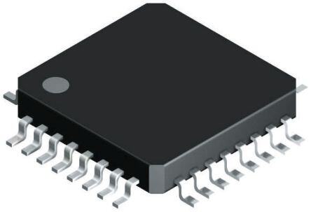
ICGOO电子元器件商城为您提供AD5763CSUZ由Analog设计生产,在icgoo商城现货销售,并且可以通过原厂、代理商等渠道进行代购。 AD5763CSUZ价格参考。AnalogAD5763CSUZ封装/规格:数据采集 - 数模转换器, 16 位 数模转换器 2 32-TQFP(7x7)。您可以下载AD5763CSUZ参考资料、Datasheet数据手册功能说明书,资料中有AD5763CSUZ 详细功能的应用电路图电压和使用方法及教程。
AD5763CSUZ 是 Analog Devices Inc. 生产的一款 16 位、双通道、串行输入、电压输出数模转换器(DAC),具有高精度和低功耗的特点。该器件广泛应用于对精度和稳定性要求较高的工业控制、测试测量设备以及通信系统中。

其主要应用场景包括:

1. 工业自动化与控制:用于高精度控制信号输出,如调节阀门、电机或传感器激励信号,适用于PLC(可编程逻辑控制器)等设备。

2. 测试与测量仪器:作为精密信号源,用于校准设备、信号发生器、示波器等仪器中,提供高分辨率和稳定性的模拟电压输出。

3. 通信设备:在基站、光模块或无线测试设备中,用于生成精确的偏置电压或调制信号。

4. 医疗设备:如诊断仪器或监测设备中,用于提供稳定的参考信号或控制信号。

5. 精密电源管理:用于可编程电源或电池测试设备中,实现对输出电压的精确调节。

AD5763CSUZ 支持±10V输出范围,具备内置基准和双缓冲架构,适合需要高稳定性和抗干扰能力的应用环境。
| 参数 | 数值 |
| 产品目录 | 集成电路 (IC)半导体 |
| 描述 | DAC 16BIT DUAL 5V 2LSB 32-TQFP数模转换器- DAC IC 16Bit +/-5v Dual 1LSB |
| 产品分类 | |
| 品牌 | Analog Devices Inc |
| 产品手册 | |
| 产品图片 |
|
| rohs | 符合RoHS无铅 / 符合限制有害物质指令(RoHS)规范要求 |
| 产品系列 | 数据转换器IC,数模转换器- DAC,Analog Devices AD5763CSUZ- |
| 数据手册 | |
| 产品型号 | AD5763CSUZ |
| PCN设计/规格 | |
| 产品培训模块 | http://www.digikey.cn/PTM/IndividualPTM.page?site=cn&lang=zhs&ptm=19145http://www.digikey.cn/PTM/IndividualPTM.page?site=cn&lang=zhs&ptm=18614http://www.digikey.cn/PTM/IndividualPTM.page?site=cn&lang=zhs&ptm=26125http://www.digikey.cn/PTM/IndividualPTM.page?site=cn&lang=zhs&ptm=26140http://www.digikey.cn/PTM/IndividualPTM.page?site=cn&lang=zhs&ptm=26150http://www.digikey.cn/PTM/IndividualPTM.page?site=cn&lang=zhs&ptm=26147 |
| 产品目录页面 | |
| 产品种类 | 数模转换器- DAC |
| 位数 | 16 |
| 供应商器件封装 | 32-TQFP(7x7) |
| 分辨率 | 16 bit |
| 包装 | 托盘 |
| 商标 | Analog Devices |
| 安装类型 | 表面贴装 |
| 安装风格 | SMD/SMT |
| 封装 | Tray |
| 封装/外壳 | 32-TQFP |
| 封装/箱体 | TQFP-32 |
| 工作温度 | -40°C ~ 105°C |
| 工厂包装数量 | 250 |
| 建立时间 | 8µs |
| 接口类型 | Serial |
| 数据接口 | 串行 |
| 最大工作温度 | + 105 C |
| 最小工作温度 | - 40 C |
| 标准包装 | 1 |
| 电压参考 | External |
| 电压源 | 双 ± |
| 电源电压-最大 | +/- 5.25 V |
| 电源电压-最小 | +/- 4.75 V |
| 积分非线性 | +/- 1 LSB |
| 稳定时间 | 10 us |
| 系列 | AD5763 |
| 结构 | R-2R |
| 设计资源 | |
| 转换器数 | 2 |
| 转换器数量 | 2 |
| 输出数和类型 | 2 电压,双极 |
| 输出类型 | Voltage |
| 采样率(每秒) | * |


- 商务部:美国ITC正式对集成电路等产品启动337调查
- 曝三星4nm工艺存在良率问题 高通将骁龙8 Gen1或转产台积电
- 太阳诱电将投资9.5亿元在常州建新厂生产MLCC 预计2023年完工
- 英特尔发布欧洲新工厂建设计划 深化IDM 2.0 战略
- 台积电先进制程称霸业界 有大客户加持明年业绩稳了
- 达到5530亿美元!SIA预计今年全球半导体销售额将创下新高
- 英特尔拟将自动驾驶子公司Mobileye上市 估值或超500亿美元
- 三星加码芯片和SET,合并消费电子和移动部门,撤换高东真等 CEO
- 三星电子宣布重大人事变动 还合并消费电子和移动部门
- 海关总署:前11个月进口集成电路产品价值2.52万亿元 增长14.8%


PDF Datasheet 数据手册内容提取
Complete Dual, 16-Bit High Accuracy, Serial Input, ±5 V DAC Data Sheet AD5763 FEATURES GENERAL DESCRIPTION Complete dual, 16-bit DAC The AD5763 is a dual, 16-bit, serial input, bipolar voltage Programmable output range output digital-to-analog converter (DAC) that operates from ±4.096 V, ±4.201 V, or ±4.311 V supply voltages of ±4.75 V up to ±5.25 V. The nominal full- ±1 LSB maximum INL error, ±1 LSB maximum DNL error scale output range is ±4.096 V. The AD5763 provides integrated Low noise: 70 nV/√Hz output amplifiers, reference buffers, and proprietary power-up/ Settling time: 10 μs maximum power-down control circuitry. The part also features a digital Integrated reference buffers I/O port, which is programmed via the serial interface. The part On-chip die temperature sensor incorporates digital offset and gain adjust registers per channel. Output control during power-up/brownout The AD5763 is a high performance converter that offers guar- Programmable short-circuit protection anteed monotonicity, integral nonlinearity (INL) of ±1 LSB, Simultaneous updating via LDAC low noise, and 10 μs settling time. During power-up (when the Asynchronous clear to zero code supply voltages are changing), the outputs are clamped to 0 V Digital offset and gain adjust via a low impedance path. Logic output control pins DSP-/microcontroller-compatible serial interface The AD5763 uses a serial interface that operates at clock rates of Temperature range: −40°C to +105°C up to 30 MHz and is compatible with DSP and microcontroller iCMOS® process technology1 interface standards. Double buffering allows the simultaneous updating of all DACs. The input coding is programmable to either APPLICATIONS twos complement or offset binary formats. The asynchronous Industrial automation clear function clears all DAC registers to either bipolar zero or Open-loop/closed-loop servo control zero scale depending on the coding used. The AD5763 is ideal Process control for both closed-loop servo control and open-loop control appli- Data acquisition systems cations. The AD5763 is available in a 32-lead TQFP, and offers Automatic test equipment guaranteed specifications over the −40°C to +105°C industrial Automotive test and measurement temperature range. Figure 1 contains a functional block diagram High accuracy instrumentation of the AD5763. Table 1. Related Devices Part No. Description AD5764 Complete quad, 16-bit, high accuracy, serial input, ±10 V output DAC AD5765 Complete quad, 16-bit, high accuracy, serial input, ±5 V DAC 1 iCMOS, Reg. U.S. Patent and Trademark Office. Rev. C Information furnished by Analog Devices is believed to be accurate and reliable. However, no responsibility is assumed by Analog Devices for its use, nor for any infringements of patents or other One Technology Way, P.O. Box 9106, Norwood, MA 02062-9106, U.S.A. rights of third parties that may result from its use. Specifications subject to change without notice. No license is granted by implication or otherwise under any patent or patent rights of Analog Devices. Tel: 781.329.4700 www.analog.com Trademarks and registered trademarks are the property of their respective owners. Fax: 781.461.3113 ©2009–2011 Analog Devices, Inc. All rights reserved.
AD5763 Data Sheet TABLE OF CONTENTS Features..............................................................................................1 Data Register...............................................................................19 Applications.......................................................................................1 Coarse Gain Register.................................................................19 General Description.........................................................................1 Fine Gain Register......................................................................20 Revision History...............................................................................2 Offset Register............................................................................20 Functional Block Diagram..............................................................3 Worked Example of Offset and Gain Adjustment.................21 Specifications.....................................................................................4 Design Features...............................................................................22 AC Performance Characteristics................................................5 Analog Output Control.............................................................22 Timing Characteristics................................................................6 Digital Offset and Gain Control...............................................22 Absolute Maximum Ratings............................................................9 Programmable Short-Circuit Protection................................22 ESD Caution..................................................................................9 Digital I/O Port...........................................................................22 Pin Configuration and Function Descriptions...........................10 Die Temperature Sensor............................................................22 Typical Performance Characteristics...........................................12 Local Ground Offset Adjust......................................................23 Terminology....................................................................................15 Power-on Status..........................................................................23 Theory of Operation......................................................................16 Applications Information..............................................................24 DAC Architecture.......................................................................16 Typical Operating Circuit.........................................................24 Reference Buffers........................................................................16 Layout Guidelines...........................................................................26 Serial Interface............................................................................16 Galvanically Isolated Interface.................................................26 Simultaneous Updating via LDAC...........................................17 Microprocessor Interfacing.......................................................26 Transfer Function.......................................................................18 Outline Dimensions.......................................................................27 Asynchronous Clear (CLR).......................................................18 Ordering Guide..........................................................................27 Function Register.......................................................................19 REVISION HISTORY 9/11—Rev. B to Rev. C Changed 50 MHz to 30 MHz Throughout....................................1 Changes to t, t, and t Parameters, Table 4..................................6 1 2 3 Changes to Table 20........................................................................25 7/11—Rev. A to Rev. B Changed 30 MHz to 50 MHz Throughout....................................1 Changes to t, t, and t Parameters, Table 4..................................6 1 2 3 Changes to Table 20........................................................................25 10/09—Rev. 0 to Rev. A Deleted Endnote 1, Table 2..............................................................4 Deleted Endnote 1, Table 3..............................................................5 Deleted Endnote 1, Table 4..............................................................6 Changes to t Parameter, Table 4....................................................6 6 1/09—Revision 0: Initial Version Rev. C | Page 2 of 28
Data Sheet AD5763 FUNCTIONAL BLOCK DIAGRAM PGND AVDD AVSS AVDD AVSS REFGND REFA RSTOUT RSTIN VOLTAGE DVCC MONITOR AD5763 REFERENCE AND DGND BUFFERS CONTROL ISCC 16 16 G1 INPUT DAC SDIN REG A REG A DAC A VOUTA INPUT SHIFT G2 SCLK REGISTER AND GAIN REG A SYNC CONTROL OFFSET REG A AGNDA LOGIC SDO 16 G1 D0 RINEPGU BT RDEAGC B DAC B VOUTB G2 D1 GAIN REG B OFFSET REG B AGNDB BIN/2sCOMP REFERENCE TEMPERATURE BUFFERS SENSOR CLR LDAC REFB TEMP 07250-001 Figure 1. Rev. C | Page 3 of 28
AD5763 Data Sheet SPECIFICATIONS AV = 4.75 V to 5.25 V, AV = −5.25 V to −4.75 V, AGNDx = DGND = REFGND = PGND = 0 V, REFA = REFB = 2.048 V, DD SS DV = 2.7 V to 5.25 V, R = 5 kΩ, C = 200 pF. All specifications T to T , unless otherwise noted. CC LOAD LOAD MIN MAX Table 2. Parameter Min Typ Max Unit Test Conditions/Comments ACCURACY Outputs unloaded Resolution 16 Bits Relative Accuracy (INL) −1 +1 LSB Differential Nonlinearity (DNL) −1 +1 LSB Guaranteed monotonic Bipolar Zero Error −2 +2 mV At 25°C −3 +3 mV Bipolar Zero Temperature ±1 ppm FSR/°C Coefficient (TC)1 Zero-Scale Error −2 +2 mV At 25°C −3.5 +3.5 mV Zero-Scale Temperature Coefficient ±1 ppm FSR/°C (TC)1 Gain Error −0.03 +0.03 % FSR At 25°C, coarse gain register = 0 −0.04 +0.04 % FSR Coarse gain register = 0 Gain Temperature Coefficient (TC)1 ±1 ppm FSR/°C DC Crosstalk1 0.5 LSB REFERENCE INPUT1 Reference Input Voltage 2.048 V nominal ±1% for specified performance DC Input Impedance 1 MΩ Typically 100 MΩ Input Current 0.03 10 μA Reference Range 1 2.1 V OUTPUT CHARACTERISTICS1 Output Voltage Range2 −4.31158 +4.31158 V Coarse gain register = 2 −4.20103 +4.20103 V Coarse gain register = 1 −4.096 +4.096 V Coarse gain register = 0 −4.42105 +4.42105 V REFA = REFB = 2.1 V, coarse gain register = 2 Output Voltage Drift vs. Time ±32 ppm FSR/500 hrs ±37 ppm FSR/1000 hrs Short-Circuit Current 10 mA RI = 6 kΩ, see Figure 23 SCC Load Current −1 +1 mA For specified performance Capacitive Load Stability R = ∞ 200 pF LOAD R = 10 kΩ 1000 pF LOAD DC Output Impedance 0.3 Ω DIGITAL INPUTS1 JEDEC compliant Input High Voltage, V 2 V IH Input Low Voltage, V 0.8 V IL Input Current −1 +1 μA Per pin Pin Capacitance 10 pF Per pin DIGITAL OUTPUTS (D0, D1, SDO)1 Output Low Voltage 0.4 V DV = 5 V ± 5%, sinking 200 μA CC Output High Voltage DV − 1 V DV = 5 V ± 5%, sourcing 200 μA CC CC Output Low Voltage 0.4 V DV = 2.7 V to 3.6 V, sinking 200 μA CC Output High Voltage DV − 0.5 V DV = 2.7 V to 3.6 V, sourcing 200 μA CC CC High Impedance Leakage Current ±1 μA SDO only High Impedance Output 5 pF SDO only Capacitance Rev. C | Page 4 of 29
Data Sheet AD5763 Parameter Min Typ Max Unit Test Conditions/Comments DIE TEMPERATURE SENSOR Output Voltage at 25°C 1.44 V Output Voltage Scale Factor 3 mV/°C Output Voltage Range 1.175 1.9 V Output Load Current 200 μA Power-On Time 10 ms POWER REQUIREMENTS AV /AV 4.75 5.25 V DD SS DV 2.7 5.25 V CC AI 2.5 3.5 mA/channel Outputs unloaded DD AI 2 3.25 mA/channel Outputs unloaded SS DI 0.75 1.2 mA V = DV , V = DGND CC IH CC IL Power Supply Sensitivity1 ∆V /∆ΑV −110 dB OUT DD Power Dissipation 45 mW ±5 V operation output unloaded 1 Guaranteed by design and characterization; not production tested. 2 Output amplifier headroom requirement is 0.5 V minimum. AC PERFORMANCE CHARACTERISTICS AV = 4.75 V to 5.25 V, AV = −5.25 V to −4.75 V, AGNDx = DGND = REFGND = PGND = 0 V, REFA = REFB = 2.048 V, DD SS DV = 2.7 V to 5.25 V, R = 5 kΩ, C = 200 pF. All specifications T to T , unless otherwise noted. CC LOAD LOAD MIN MAX Table 3. Parameter Min Typ Max Unit Test Conditions/Comments DYNAMIC PERFORMANCE1 Output Voltage Settling Time 8 μs Full-scale step to ±1 LSB 10 μs 2 μs 512 LSB step settling Slew Rate 5 V/μs Digital-to-Analog Glitch Energy 20 nV-sec Glitch Impulse Peak Amplitude 30 mV Channel-to-Channel Isolation 60 dB DAC-to-DAC Crosstalk 8 nV-sec Digital Crosstalk 2 nV-sec Digital Feedthrough 2 nV-sec Effect of input bus activity on DAC outputs Output Noise (0.1 Hz to 10 Hz) 0.1 LSB p-p Output Noise (0.1 Hz to 100 kHz) 50 μV rms 1/f Corner Frequency 300 Hz Output Noise Spectral Density 70 nV/√Hz Measured at 10 kHz Complete System Output Noise Spectral Density2 80 nV/√Hz Measured at 10 kHz 1 Guaranteed by design and characterization; not production tested. 2 Includes noise contributions from integrated reference buffers, 16-bit DAC, and output amplifier. Rev. C | Page 5 of 28
AD5763 Data Sheet TIMING CHARACTERISTICS AV = 4.75 V to 5.25 V, AV = −5.25 V to −4.75 V, AGNDx = DGND = REFGND = PGND = 0 V, REFA = REFB = 2.048 V, DD SS DV = 2.7 V to 5.25 V, R = 5 kΩ, C = 200 pF. All specifications T to T , unless otherwise noted. CC LOAD LOAD MIN MAX Table 4. Parameter1, 2, 3 Limit at T , T Unit Description MIN MAX t 33 ns min SCLK cycle time 1 t 13 ns min SCLK high time 2 t 13 ns min SCLK low time 3 t 13 ns min SYNC falling edge to SCLK falling edge setup time 4 t 4 13 ns min 24th SCLK falling edge to SYNC rising edge 5 t 90 ns min Minimum SYNC high time 6 t 2 ns min Data setup time 7 t 5 ns min Data hold time 8 t 1.7 μs min SYNC rising edge to LDAC falling edge (all DACs updated) 9 480 ns min SYNC rising edge to LDAC falling edge (single DAC updated) t 10 ns min LDAC pulse width low 10 t 500 ns max LDAC falling edge to DAC output response time 11 t 10 μs max DAC output settling time 12 t 10 ns min CLR pulse width low 13 t 2 μs max CLR pulse activation time 14 t 5, 6 25 ns max SCLK rising edge to SDO valid 15 t 13 ns min SYNC rising edge to SCLK falling edge 16 t 2 μs max SYNC rising edge to DAC output response time (LDAC= 0) 17 t 170 ns min LDAC falling edge to SYNC rising edge 18 1 Guaranteed by design and characterization; not production tested. 2 All input signals are specified with tR = tF = 5 ns (10% to 90% of DVCC) and timed from a voltage level of 1.2 V. 3 See Figure 2, Figure 3, and Figure 4. 4 Standalone mode only. 5 Measured with the load circuit of Figure 5. 6 Daisy-chain mode only. Rev. C | Page 6 of 28
Data Sheet AD5763 t 1 SCLK 1 2 24 t6 t3 t2 t4 t5 SYNC t 8 t 7 SDIN DB23 DB0 t10 t t10 9 LDAC t18 t12 t 11 VOUTx LDAC = 0 t 12 t 17 VOUTx t CLR 13 t 14 VOUTx 07250-002 Figure 2. Serial Interface Timing Diagram t 1 SCLK 24 48 t6 t3 t2 t5 t t 16 4 SYNC t 8 t 7 SDIN DB23 DB0 DB23 DB0 INPUT WORD FOR DAC N INPUT WORD FOR DAC N – 1 t 15 SDO DB23 DB0 UNDEFINED INPUT WORD FOR DAC N t9 t 10 LDAC 07250-003 Figure 3. Daisy-Chain Timing Diagram Rev. C | Page 7 of 28
AD5763 Data Sheet SCLK 24 48 SYNC SDIN DB23 DB0 DB23 DB0 INPUT WORD SPECIFIES NOP CONDITION REGISTER TO BE READ SDO DB23 DB0 UNDEFINED SELECCTLEOD CRKEEGDIS OTUETR DATA 07250-004 Figure 4. Readback Timing Diagram 200µA IOL TO OUTPUT VOH (MIN) OR PIN CL VOL (MAX) 50pF 200µA IOH 07250-005 Figure 5. Load Circuit for SDO Timing Diagram Rev. C | Page 8 of 28
Data Sheet AD5763 ABSOLUTE MAXIMUM RATINGS T = 25°C, unless otherwise noted. Transient currents of up to Stresses above those listed under Absolute Maximum Ratings A 100 mA do not cause SCR latch-up. may cause permanent damage to the device. This is a stress rating only; functional operation of the device at these or any Table 5. other conditions above those listed in the operational sections Parameter Rating of this specification is not implied. Exposure to absolute AVDD to AGNDx, DGND −0.3 V to +7 V maximum rating conditions for extended periods may affect AVSS to AGNDx, DGND +0.3 V to −7 V device reliability. DV to DGND −0.3 V to +7 V CC DV to AVDD −DV to +0.25 V CC CC Digital Inputs to DGND −0.3 V to DV + 0.3 V or 7 V ESD CAUTION CC (whichever is less) Digital Outputs to DGND −0.3 V to DV + 0.3 V CC REFx to AGNDx, PGND −0.3 V to AV + 0.3 V DD VOUTx to AGNDx AV to AV SS DD AGNDx to DGND −0.3 V to +0.3 V Operating Temperature Range (T ) A Industrial −40°C to +105°C Storage Temperature Range −65°C to +150°C Junction Temperature (T max) 150°C J Power Dissipation (T max – T )/θ J A JA 32-Lead TQFP θ Thermal Impedance 65°C/W JA θ Thermal Impedance 12°C/W JC Lead Temperature JEDEC industry standard Soldering J-STD-020 Rev. C | Page 9 of 28
AD5763 Data Sheet PIN CONFIGURATION AND FUNCTION DESCRIPTIONS P M BIN/2sCO AVDDAVSSTEMP REFGND NC REFB REFA 32 25 1 24 SYNC NC PIN 1 SCLK INDICATOR NC SDIN VOUTA SDO AD5763 AGNDA CLR TOP VIEW AGNDB (Not to scale) LDAC VOUTB D0 NC D1 NC 8 17 9 16 T N D C DD SC RSTOU NRSTIC DGN= NODVC CAVODNPGNNECAVST ISC 07250-006 Figure 6. Pin Configuration Table 6. Pin Function Descriptions Pin No. Mnemonic Description 1 SYNC Active Low Input. This pin is the frame synchronization signal for the serial interface. While SYNC is low, data is transferred in on the falling edge of SCLK. 2 SCLK Serial Clock Input. Data is clocked into the shift register on the falling edge of SCLK. This pin operates at clock speeds up to 30 MHz. 3 SDIN Serial Data Input. Data must be valid on the falling edge of SCLK. 4 SDO Serial Data Output. Used to clock data from the serial register in daisy-chain or readback mode. 51 CLR Negative Edge Triggered Input. Asserting this pin sets the DAC registers to 0x0000.1 6 LDAC Load DAC. Logic input. This pin is used to update the DAC registers and consequently the analog outputs. When LDAC is tied permanently low, the addressed DAC register is updated on the rising edge of SYNC. If LDAC is held high during the write cycle, the DAC input register is updated but the output update is held off until the falling edge of LDAC. In this mode, all analog outputs can be updated simultaneously on the falling edge of LDAC. The LDAC pin must not be left unconnected. 7, 8 D0, D1 D0 and D1 form a digital I/O port. The user can set up these pins as inputs or outputs that are confi- gurable and readable over the serial interface. When configured as inputs, these pins have weak internal pull-ups to DV . When programmed as outputs, D0 and D1 are referenced by DV and DGND. CC CC 9 RSTOUT Reset Logic Output. This pin is the output from the on-chip voltage monitor used in the reset circuit. If desired, it can be used to control other system components. 10 RSTIN Reset Logic Input. This input allows external access to the internal reset logic. Applying a Logic 0 to this input clamps the DAC outputs to 0 V. In normal operation, RSTIN should be tied to Logic 1. Register values remain unchanged. 11 DGND Digital Ground Pin. 12 DV Digital Supply Pin. The voltage ranges from 2.7 V to 5.25 V. CC 13, 31 AV Positive Analog Supply Pins. The voltage ranges from 4.75 V to 5.25 V. DD 14 PGND Ground Reference Point for Analog Circuitry. 15, 30 AV Negative Analog Supply Pins. The voltage ranges from –5.25 V to –4.75 V. SS 16 ISCC This pin is used in association with an optional external resistor connected to AGND and programs the short-circuit current of the output amplifiers. See the Design Features section for further details. 17, 18, 23, 24, 27 NC No Connect. 19 VOUTB Analog Output Voltage of DAC B. Buffered output with a nominal full-scale output range of ±4.096 V. The output amplifier is capable of directly driving a 5 kΩ, 200 pF load. 20 AGNDB Ground Reference Pin for the DAC B Output Amplifier. 21 AGNDA Ground Reference Pin for the DAC A Output Amplifier. Rev. C | Page 10 of 29
Data Sheet AD5763 Pin No. Mnemonic Description 22 VOUTA Analog Output Voltage of DAC A. Buffered output with a nominal full-scale output range of ±4.096 V. The output amplifier is capable of directly driving a 5 kΩ, 200 pF load. 25 REFA Reference Voltage Input. The reference input range is 1 V to 2.1 V. This pin programs the full-scale output voltage. REFA = 2.048 V for specified performance. 26 REFB Reference Voltage Input. The reference input range is 1 V to 2.1 V. This pin programs the full-scale output voltage. REFB = 2.048 V for specified performance. 28 REFGND Reference Ground Return for the Reference Generator and Buffers. 29 TEMP This pin provides an output voltage proportional to temperature. The output voltage is 1.44 V typical at 25°C die temperature; variation with temperature is 3 mV/°C. 32 BIN/2sCOMP Determines the DAC Coding. This pin should be hardwired to either DV or DGND. When CC hardwired to DV , the input coding is offset binary. When hardwired to DGND, the input coding is CC twos complement (see Table 7). 1 Internal pull-up device on this logic input. Therefore, it can be left floating and defaults to a logic high condition. Rev. C | Page 11 of 29
AD5763 Data Sheet TYPICAL PERFORMANCE CHARACTERISTICS 1.0 0.30 0.8 TA = 25°C 0.25 0.6 0.20 0.15 0.4 Bs) Bs) 0.10 R (LS 0.2 R (LS 0.05 O 0 O RR RR 0 NL E –0.2 NL E 0.05 I –0.4 D 0.10 –0.6 –0.15 –0.8 –0.20 –1.00 10,000 20,000 30,0C0O0DE40,000 50,000 60,000 07250-007 –0.25–40 –20 0 TEM2P0ERATU4R0E (°C)60 80 100 07250-010 Figure 7. Integral Nonlinearity Error vs. Code Figure 10. Differential Nonlinearity Error vs. Temperature 1.0 5.5 0.8 TA = 25°C 5.3 0.6 5.1 s) 0.4 AIDD B 4.9 R (LS 0.2 mA) 4.7 RO 0 (S L ER –0.2 /AIDS 4.5 N D 4.3 D –0.4 AI 4.1 –0.6 AISS 3.9 –0.8 3.7 –1.00 10,000 20,000 30,0C0O0DE40,000 50,000 60,000 07250-008 3.54.5 4.6 4.7 4.8 4A.9VDD/5A.V0SS (5V.1) 5.2 5.3 5.4 5.5 07250-016 Figure 8. Differential Nonlinearity Error vs. Code Figure 11. AIDD/AISS vs. AVDD/AVSS 0.4 0.80 0.3 0.75 0.2 mV) SBs) OR ( 0.70 R (L 0.1 ERR RRO 0 ALE 0.65 E C INL –0.1 RO-S 0.60 E Z 0.55 –0.2 –0.–340 –20 0 TEM2P0ERATU4R0E (°C)60 80 100 07250-009 0.50–40 –20 0 TEM2P0ERATU4R0E (°C)60 80 100 07250-017 Figure 9. Integral Nonlinearity Error vs. Temperature Figure 12. Zero-Scale Error vs. Temperature Rev. C | Page 12 of 28
Data Sheet AD5763 0.20 2.0 AVDD = +5V 0.18 1.5 AVSS = –5V R (mV)0.16 TA (mV) 1.0 TA = 25°C ERRO0.14 E DEL 0.5 R ZERO 0.12 VOLTAG –0.50 BIPOLA0.10 UTPUT –1.0 O 0.08 –1.5 0.06–40 –20 0 TEM2P0ERATU4R0E (°C)60 80 100 07250-018 –2.0–8 –6 –4 S–O2URCE0/SINK C2URREN4T (mA6) 8 1007250-021 Figure 13. Bipolar Zero Error vs. Temperature Figure 16. Source and Sink Capability of Output Amplifier with Positive Full- Scale Loaded 4 –0.008 AVDD = +5V –0.009 V) 3 ATAV S=S 2 =5 °–C5V m 2 –0.010 A ( %FSR) –0.011 E DELT 1 R ( AG 0 O –0.012 T R L R O E V –1 N –0.013 T GAI TPU –2 –0.014 OU –3 –0.015 –0.016–40 –20 0 TEM2P0ERATU4R0E (°C)60 80 100 07250-019 –4–10 –8 –6 –4SOUR–C2E/SIN0K CUR2RENT4 (mA)6 8 1007250-022 Figure 14. Gain Error vs. Temperature Figure 17. Source and Sink Capability of Output Amplifier with Negative Full- Scale Loaded 4.0 3.5 TA = 25°C 3.0 2.5 A) m ( 2.0 C DIC 1 1.5 1.0 0.5 00 1 LOGI2CINPUTVO3LTAGE(V)4 5 07250-020 CH1 1.25V M1.00µs CH1 –175mV 07250-023 Figure 15. DICC vs. Logic Input Voltage Figure 18. Positive Full-Scale Step Rev. C | Page 13 of 28
AD5763 Data Sheet 1 2 1 3 CH1 1.25V M1.00µs CH1 175mV 07250-024 CCHH13 55.00.00VmV CH2 5.00V M25.0ms CH1 4.1V 07250-028 Figure 19. Negative Full-Scale Step Figure 22. VOUTx vs. AVDD/AVSS on Power-Up 10 40 TA = 25°C 0x7FFF TO 0x8000 9 TA = 25°C 30 0x8000 TO 0x7FFF A) 8 m mV) 20 NT ( 7 GE ( 10 RRE 6 A U T C VOL 0 UIT 5 PUT –10 CIRC 4 OUT –20 SHORT- 23 –30 1 0 –40–1.0 –0.5 0 0.5TIME1 (.µ0s) 1.5 2.0 2.5 3.0 07250-026 1 2 3 4 5RISCC6(kΩ) 7 8 9 1007250-029 Figure 20. Major Code Transition Glitch Energy Figure 23. Short-Circuit Current vs. RISCC 1.8 AVDD = +5V AVSS = –5V 1.7 V) E ( G A 1.6 T L O V UT 1.5 P 4 T U O P 1.4 M E T 1.3 CH4 50µV M1.00µs CH4 26µV 07250-027 1.2–40 –20 0 TEM2P0ERATU4R0E (°C)60 80 100 07250-030 Figure 21. Peak-to-Peak Noise (100 kHz Bandwidth) Figure 24. TEMP Output Voltage vs. Temperature Rev. C | Page 14 of 28
Data Sheet AD5763 TERMINOLOGY Relative Accuracy or Integral Nonlinearity (INL) Total Unadjusted Error (TUE) For the DAC, relative accuracy or INL is a measure of the TUE is a measure of the output error considering all the various maximum deviation, in LSBs, from a straight line passing errors. through the endpoints of the DAC transfer function. A typical Zero-Scale Error Temperature Coefficient (TC) INL vs. code plot can be seen in Figure 7. Zero-scale error TC is a measure of the change in zero-scale Differential Nonlinearity (DNL) error with a change in temperature. Zero-scale error TC is DNL is the difference between the measured change and the expressed in ppm FSR/°C. ideal 1 LSB change between any two adjacent codes. A specified Gain Error Temperature Coefficient (TC) differential nonlinearity of ±1 LSB maximum ensures mono- Gain error TC is a measure of the change in gain error with tonicity. This DAC is guaranteed monotonic. A typical DNL changes in temperature. Gain error TC is expressed in ppm vs. code plot can be seen in Figure 8. FSR/°C. Monotonicity Digital-to-Analog Glitch Energy A DAC is monotonic if the output either increases or remains Digital-to-analog glitch energy is the impulse injected into the constant for the increasing digital input code. The AD5763 is analog output when the input code in the DAC register changes monotonic over its full operating temperature range. state. It is normally specified as the area of the glitch in nV-sec and Bipolar Zero Error is measured when the digital input code is changed by 1 LSB at the Bipolar zero error is the deviation of the analog output from the major carry transition glitch (0x7FFF to 0x8000) (see Figure 20). ideal half-scale output of 0 V when the DAC register is loaded Digital Feedthrough with 0x8000 (offset binary coding) or 0x0000 (twos complement Digital feedthrough is a measure of the impulse injected into coding). A plot of bipolar zero error vs. temperature can be seen the analog output of the DAC from the digital inputs of the DAC, in Figure 13. but is measured when the DAC output is not updated. It is Bipolar Zero Temperature Coefficient (TC) specified in nV-sec and measured with a full-scale code change Bipolar zero TC is the measure of the change in the bipolar zero on the data bus, that is, from all 0s to all 1s, and vice versa. error with a change in temperature. It is expressed in ppm FSR/°C. Power Supply Sensitivity Full-Scale Error Power supply sensitivity indicates how the output of the DAC Full-scale error is a measure of the output error when full-scale is affected by changes in the power supply voltage. code is loaded to the DAC register. Ideally, the output voltage DC Crosstalk should be 2 × V − 1 LSB. Full-scale error is expressed in REF DC crosstalk is the dc change in the output level of one DAC percentage of full-scale range. in response to a change in the output of another DAC. It is Negative Full-Scale Error/Zero-Scale Error measured with a full-scale output change on one DAC while Negative full-scale error is the error in the DAC output voltage monitoring another DAC, and is expressed in LSB. when 0x0000 (offset binary coding) or 0x8000 (twos complement DAC-to-DAC Crosstalk coding) is loaded to the DAC register. Ideally, the output voltage DAC-to-DAC crosstalk is the glitch impulse transferred to the should be −2 × V . A plot of zero-scale error vs. temperature REF output of one DAC due to a digital code change and subsequent can be seen in Figure 12. output change of another DAC. This includes both digital and Output Voltage Settling Time analog crosstalk. It is measured by loading one of the DACs by Output voltage settling time is the amount of time it takes for the a full-scale code change (all 0s to all 1s and vice versa) with output to settle to a specified level for a full-scale input change. LDAC low and monitoring the output of another DAC. The Slew Rate energy of the glitch is expressed in nV-sec. The slew rate of a device is a limitation in the rate of change Channel-to-Channel Isolation of the output voltage. The output slewing speed of a voltage- Channel-to-channel isolation is the ratio of the amplitude of the output DAC is usually limited by the slew rate of the amplifier signal at the output of one DAC to a sine wave on the reference used at its output. Slew rate is measured from 10% to 90% of input of another DAC. It is measured in decibels. the output signal and is expressed in volts per microsecond. Digital Crosstalk Gain Error Digital crosstalk is a measure of the impulse injected into the Gain error is a measure of the span error of the DAC. It is the analog output of one DAC from the digital inputs of another deviation in slope of the DAC transfer characteristic from the DAC, but is measured when the DAC output is not updated. ideal, expressed as a percentage of the full-scale range. A plot It is specified in nV-sec and measured with a full-scale code of gain error vs. temperature can be seen in Figure 14. change on the data bus, that is, from all 0s to all 1s, and vice versa. Rev. C | Page 15 of 28
AD5763 Data Sheet THEORY OF OPERATION The AD5763 is a dual, 16-bit, serial input, bipolar voltage SERIAL INTERFACE output DAC and operates from supply voltages of ±4.75 V to The AD5763 is controlled over a versatile 3-wire serial interface ±5.25 V. The part has a specified buffered output voltage of up that operates at clock rates of up to 30 MHz and is compatible to ±4.311 V. Data is written to the AD5763 in a 24-bit word with SPI, QSPI™, MICROWIRE™, and DSP standards. format via a 3-wire serial interface. The device also offers an Input Shift Register SDO pin, which is available for daisy-chaining or readback. The input shift register is 24 bits wide. Data is loaded into the The AD5763 incorporates a power-on reset circuit, which device MSB first as a 24-bit word under the control of a serial ensures that the DAC registers power-up loaded with 0x0000. clock input, SCLK. The input register consists of a read/write The AD5763 features a digital I/O port that can be programmed bit, three register select bits, three DAC address bits and 16 via the serial interface, on-chip reference buffers, per channel data bits as shown in Table 8. The timing diagram for this digital gain, and offset registers. operation is shown in Figure 2. DAC ARCHITECTURE Upon power-up, the DAC registers are loaded with zero code The DAC architecture of the AD5763 consists of a 16-bit (0x0000) and the outputs are clamped to 0 V via a low impedance current mode segmented R-2R ladder DAC. The simplified path. The outputs can be updated with the zero code value at this circuit diagram for the DAC section is shown in Figure 25. time by asserting either LDAC or CLR. The corresponding output The four MSBs of the 16-bit data-word are decoded to drive voltage depends on the state of the BIN/2sCOMP pin. If BIN/ 15 switches, E1 to E15. Each of these switches connects one 2sCOMP is tied to DGND, then the data coding is twos comple- of the 15 matched resistors to either AGNDx or IOUT. The ment and the outputs update to 0 V. If the BIN/2sCOMP pin is remaining 12 bits of the data-word drive Switch S0 to Switch tied to DV , then the data coding is offset binary and the outputs CC S11 of the 12-bit R-2R ladder network. update to negative full-scale. To have the outputs power-up with VREF R R R zero code loaded to the outputs, the CLR pin should be held low during power-up. 2R 2R 2R 2R 2R 2R 2R Standalone Operation R/8 The serial interface works with both a continuous and noncon- E15 E14 E1 S11 S10 S0 tinuous serial clock. A continuous SCLK source can only be IOUT used if SYNC is held low for the correct number of clock cycles. VOUTx In gated clock mode, a burst clock containing the exact number AGNDx 41 M5 SEBQsU DAELC SOEDGEMDE INNTTSO 12-BIT, R-2R LADDER 07250-031 othf ec lfoincakl ccyloclceks tmo ulasttc bhe t uhsee dda atan.d T ShYeN fiCrs tm faulslti nbge etdakgeen o fh SigYhN aCft er Figure 25. DAC Ladder Structure starts the write cycle. Exactly 24 falling clock edges must be REFERENCE BUFFERS applied to SCLK before SYNC is brought high again. If SYNC is The AD5763 operates with an external reference. The reference brought high before the 24th falling SCLK edge, then the data inputs (REFA and REFB) have an input range up to 2.1 V. This written is invalid. If more than 24 falling SCLK edges are input voltage is then used to provide a buffered positive and applied before SYNC is brought high, then the input data negative reference for the DAC cores. The positive reference is also invalid. The addressed input register is updated on the (V ) is given by rising edge of SYNC. For another serial transfer to take place, REFP SYNC must be brought low again. After the end of the serial V = 2V REFP REF data transfer, data is automatically transferred from the input The negative reference (V ) to the DAC cores is given by REFN shift register to the addressed register. V = −2V REFN REF When the data has been transferred into the chosen register These positive and negative reference voltages (along with the of the addressed DAC, all DAC registers and outputs can be gain register values) define the output ranges of the DACs. updated by taking LDAC low. Rev. C | Page 16 of 28
Data Sheet AD5763 SDO disable bit; this bit is cleared by default. Readback mode 68HC111 AD57631 is invoked by setting the R/W bit to 1 in the serial input register MOSI SDIN write. When R/W is 1, Bit A2 to Bit A0 select the register to be SCK SCLK read in association with Bit REG2, Bit REG1, and Bit REG0. PC7 SYNC The remaining data bits in the write sequence are don’t cares. PC6 LDAC During the next SPI write, the data appearing on the SDO output MISO SDO contains the data from the previously addressed register. For a read of a single register, the NOP command can be used in SDIN clocking out the data from the selected register on SDO. The AD57631 readback diagram in Figure 4 shows the readback sequence. For example, to read back the fine gain register of Channel A SCLK on the AD5763, the following sequence should be implemented: SYNC LDAC 1. Write 0xA0XXXX to the AD5763 input register. This SDO configures the AD5763 for read mode with the fine gain register of Channel A selected. Note that all the data bits, DB15 to DB0, are don’t cares. SDIN 2. Follow this with a second write: 0x00XXXX, which is an AD57631 NOP condition. During this write, the data from the fine SCLK gain register is clocked out on the SDO line, that is, data SYNC clocked out contains the data from the fine gain register LDAC in Bit DB5 to Bit DB0. SDO SIMULTANEOUS UPDATING VIA LDAC 1ADDITIONAL PINS OMITTED FOR CLARITY. 07250-032 Depending on the status of both SYNC and LDAC, and after Figure 26. Daisy-Chaining the AD5763 data has been transferred into the input register of the DACs, Daisy-Chain Operation there are two ways in which the DAC registers and DAC outputs can be updated. For systems that contain several devices, the SDO pin can be used to daisy-chain multiple devices together. This daisy-chain Individual DAC Updating mode can be useful in system diagnostics and in reducing the In this mode, LDAC is held low while data is being clocked into number of serial interface lines. The first falling edge of SYNC the input shift register. The addressed DAC output is updated starts the write cycle. The SCLK is continuously applied to the on the rising edge of SYNC. input shift register when SYNC is low. If more than 24 clock Simultaneous Updating of All DACs pulses are applied, the data ripples out of the shift register and appears on the SDO line. This data is clocked out on the rising In this mode, LDAC is held high while data is being clocked edge of SCLK and is valid on the falling edge. By connecting the into the input shift register. All DAC outputs are updated by SDO of the first device to the SDIN input of the next device in taking LDAC low any time after SYNC has been taken high. the chain, a multidevice interface is constructed. Each device in The update now occurs on the falling edge of LDAC. the system requires 24 clock pulses. Therefore, the total number OUTPUT of clock cycles must equal 24n, where n is the total number of I/V AMPLIFIER AD5763 devices in the chain. When the serial transfer to all REFA, REFB 16-BIT VOUTx DAC devices is complete, SYNC is taken high. This latches the input data in each device in the daisy chain and prevents any further DAC data from being clocked into the input shift register. The SCLK LDAC REGISTER can be a continuous or a gated clock. A continuous SCLK source can only be used if SYNC is held INPUT REGISTER low for the correct number of clock cycles. In gated clock mode, a burst clock containing the exact number of clock cycles must blaet cuhs ethde a dnadt aS.Y NC must be taken high after the final clock to SSSYCDNLICKN INTLEORGFIACCE SDO 07250-033 Figure 27. Simplified Serial Interface of Input Loading Circuitry Readback Operation for One DAC Channel Before a readback operation is initiated, the SDO pin must be enabled by writing to the function register and clearing the Rev. C | Page 17 of 28
AD5763 Data Sheet TRANSFER FUNCTION The output voltage expression for the AD5763 is given by Table 7 shows the ideal input code to output voltage relationship ⎡ D ⎤ for the AD5763 for both offset binary and twos complement VOUTx=−2×VREFIN +4×VREFIN⎢⎣65,536⎥⎦ data coding. where: Table 7. Ideal Output Voltage to Input Code Relationship D is the decimal equivalent of the code loaded to the DAC. Digital Input Analog Output V is the reference voltage applied at the REFA and REFB pins. REFIN Offset Binary Data Coding MSB LSB VOUTx ASYNCHRONOUS CLEAR (CLR) 1111 1111 1111 1111 +2V × (32,767/32,768) REF CLR is a negative edge triggered clear that allows the outputs to 1000 0000 0000 0001 +2V × (1/32,768) REF be cleared to either 0 V (twos complement coding) or negative 1000 0000 0000 0000 0 V full scale (offset binary coding). It is necessary to keep CLR low 0111 1111 1111 1111 −2VREF × (1/32,768) for a minimum amount of time for the operation to complete (see 0000 0000 0000 0000 −2VREF × (32,767/32,768) Figure 2). When the CLR signal is returned high, the output Twos Complement Data Coding remains at the cleared value until a new value is programmed. MSB LSB VOUTx If at power-on, CLR is at 0 V, all DAC outputs are updated with 0111 1111 1111 1111 +2V × (32,767/32,768) REF the clear value. A clear can also be initiated through software by 0000 0000 0000 0001 +2VREF × (1/32,768) writing a command, 0x04XXXX, to the AD5763. 0000 0000 0000 0000 0 V 1111 1111 1111 1111 −2V × (1/32,768) REF 1000 0000 0000 0000 −2V × (32,767/32,768) REF Table 8. Input Register Format MSB LSB DB23 DB22 DB21 DB20 DB19 DB18 DB17 DB16 DB15:DB0 R/W 0 REG2 REG1 REG0 A2 A1 A0 Data Table 9. Input Register Bit Functions Bit Description R/W Indicates a read from or a write to the addressed register REG2, REG1, REG0 These bits are used in association with the address bits to determine if a read or write operation is sent to the function register, data register, offset register, or gain register REG2 REG1 REG0 Function 0 0 0 Function register 0 1 0 Data register 0 1 1 Coarse gain register 1 0 0 Fine gain register 1 0 1 Offset register A2, A1, A0 These bits are used to decode the DAC channels A2 A1 A0 Channel Address 0 0 0 DAC A 0 0 1 DAC B 1 0 0 Both DACs D15:D0 Data bits Rev. C | Page 18 of 28
Data Sheet AD5763 FUNCTION REGISTER The function register is addressed by setting the three REG bits to 000. The values written to the address bits and the data bits determine the function addressed. The functions available via the function register are outlined in Table 10 and Table 11. Table 10. Function Register Options REG2 REG1 REG0 A2 A1 A0 DB15:DB6 DB5 DB4 DB3 DB2 DB1 DB0 0 0 0 0 0 0 NOP, data = don’t care 0 0 0 0 0 1 Don’t care Local-ground-offset D1 D1 D0 D0 SDO adjust direction value direction value disable 0 0 0 1 0 0 Clear, data = don’t care 0 0 0 1 0 1 Load, data = don’t care Table 11. Explanation of Function Register Options Option Description NOP No operation instruction used in readback operations. Local-Ground- Set by the user to enable local-ground-offset adjust function. Cleared by the user to disable local-ground-offset adjust Offset Adjust function (default). See the Design Features section for further details. D0/D1 Direction Set by the user to enable D0, D1 as outputs. Cleared by the user to enable D0, D1 as inputs (default). See the Design Features section for further details. D0/D1 Value I/O port status bits. Logic values written to these locations determine the logic outputs on the D0 and D1 pins when configured as outputs. These bits indicate the status of the D0 and D1 pins when the I/O port is active as an input. When enabled as inputs, these bits are don’t cares during a write operation. SDO Disable Set by the user to disable the SDO output. Cleared by the user to enable the SDO output (default). Clear Addressing this function resets the DAC outputs to 0 V in twos complement mode and negative full scale in binary mode. Load Addressing this function updates the DAC registers and, consequently, the analog outputs. DATA REGISTER The data register is addressed by setting the three REG bits to 010. The DAC address bits select with which DAC channel the data transfer is to take place (see Table 9). The data bits are in Position DB15 to Position DB0 as shown in Table 12. Table 12. Programming the Data Register REG2 REG1 REG0 A2 A1 A0 DB15 … DB0 0 1 0 DAC address 16-bit DAC data COARSE GAIN REGISTER The coarse gain register is addressed by setting the three REG bits to 011. The DAC address bits select with which DAC channel the data transfer is to take place (see Table 9). The coarse gain register is a 2-bit register and allows the user to select the output range of each DAC as shown in Table 13 and Table 14. Table 13. Programming the Coarse Gain Register REG2 REG1 REG0 A2 A1 A0 DB15:DB2 DB1 DB0 0 1 1 DAC address Don’t care CG1 CG0 Table 14. Output Range Selection Output Range CG1 CG0 ±4.096 V (Default) 0 0 ±4.20103 V 0 1 ±4.31158 V 1 0 Rev. C | Page 19 of 28
AD5763 Data Sheet FINE GAIN REGISTER The fine gain register is addressed by setting the three REG bits to 100. The DAC address bits select with which DAC channel the data transfer is to take place (see Table 9). The fine gain register is a 6-bit register and allows the user to adjust the gain of each DAC channel by −32 LSB to +31 LSB in 1 LSB increments as shown in Table 15 and Table 16. The adjustment is made to both the positive full-scale and negative full-scale points simultaneously, each point being adjusted by ½ of one step. The fine gain register coding is twos complement. Table 15. Programming Fine Gain Register REG2 REG1 REG0 A2 A1 A0 DB15:DB6 DB5 DB4 DB3 DB2 DB1 DB0 1 0 0 DAC address Don’t care FG5 FG4 FG3 FG2 FG1 FG0 Table 16. Fine Gain Register Options Gain Adjustment FG5 FG4 FG3 FG2 FG1 FG0 +31 LSB 0 1 1 1 1 1 +30 LSB 0 1 1 1 1 0 … … … … … … … No Adjustment (Default) 0 0 0 0 0 0 … … … … … … … −31 LSB 1 0 0 0 0 1 −32 LSB 1 0 0 0 0 0 OFFSET REGISTER The offset register is addressed by setting the three REG bits to 101. The DAC address bits select with which DAC channel the data transfer is to take place (see Table 9). The AD5763 offset register is an 8-bit register and allows the user to adjust the offset of each channel by −16 LSB to +15.875 LSB in increments of ⅛ LSB as shown in Table 17 and Table 18. The offset register coding is twos complement. Table 17. Programming the Offset Register REG2 REG1 REG0 A2 A1 A0 DB15:DB8 DB7 DB6 DB5 DB4 DB3 DB2 DB1 DB0 1 0 1 DAC address Don’t care OF7 OF6 OF5 OF4 OF3 OF2 OF1 OF0 Table 18. Offset Register Options Offset Adjustment OF7 OF6 OF5 OF4 OF3 OF2 OF1 OF0 +15.875 LSB 0 1 1 1 1 1 1 1 +15.75 LSB 0 1 1 1 1 1 1 0 … … … … … … … … … No Adjustment (Default) 0 0 0 0 0 0 0 0 … … … … … … … … … −15.875 LSB 1 0 0 0 0 0 0 1 −16 LSB 1 0 0 0 0 0 0 0 Rev. C | Page 20 of 28
Data Sheet AD5763 Removing Gain Error WORKED EXAMPLE OF OFFSET AND GAIN ADJUSTMENT The AD5763 can eliminate a gain error at negative full-scale output in the range of −2 mV to +1.94 mV with a step size of Using the information provided in the previous section, the ½ of a 16-bit LSB. following worked example demonstrates how the functions of the AD5763 can be used to eliminate both offset and gain Calculate the step size of the gain adjustment errors. Because the AD5763 is factory calibrated, offset and 8.192 gain errors should be negligible. However, errors can be intro- GainAdjustStepSize= =62.5μV 216×2 duced by the system that the AD5763 is operating within; for example, a voltage reference value that is not equal to 2.048 V Measure the gain error by programming 0x8000 to the data introduces a gain error. An output range of ±4.096 V and twos register and measure the resulting output voltage. The gain complement data coding is assumed. error is the difference between this value and −4.096 V; for this example, the gain error is −0.8 mV. Removing Offset Error Calculate how many gain adjustment steps this value represents The AD5763 can eliminate an offset error in the range of −2 mV to +1.98 mV with a step size of ⅛ of a 16-bit LSB. MeasuredGainValue 0.8mV Numberof Steps= = =13Steps Calculate the step size of the offset adjustment using the GainStepSize 62.5μV following equation: The gain error measured is negative (in terms of magnitude); 8.192 therefore, a positive adjustment of 13 steps is required. The gain Offset AdjustStepSize= =15.625μV 216×8 register is six bits wide and the coding is twos complement, the required gain register value can be determined as follows: Measure the offset error by programming 0x0000 to the data Convert adjustment value to binary: 001101. register and measuring the resulting output voltage. For this The value to be programmed to the gain register is simply this example, the measured value is 614 μV. binary number. Calculate the number of offset adjustment steps that this value represents, MeasuredOffsetValue 614μV Numberof Steps= = =40Steps OffsetStepSize 15.625μV The offset error measured is positive, therefore, a negative adjustment of 40 steps is required. The offset register is 8 bits wide and the coding is twos complement. The required offset register value can be calculated as follows: Convert adjustment value to binary: 00101000. Convert this to a negative twos complement number by inverting all bits and adding 1: 11011000. 11011000 is the value that should be programmed to the offset register. Note that this twos complement conversion is not necessary in the case of a positive offset adjustment. The value to be programmed to the offset register is simply the binary representation of the adjustment value. Rev. C | Page 21 of 28
AD5763 Data Sheet DESIGN FEATURES ANALOG OUTPUT CONTROL PROGRAMMABLE SHORT-CIRCUIT PROTECTION In many industrial process control applications, it is vital that The short-circuit current, ISC, of the output amplifiers can be the output voltage be controlled during power-up and during programmed by inserting an external resistor between the brownout conditions. When the supply voltages change, the ISCC pin and PGND. The programmable range for the current output pins are clamped to 0 V via a low impedance path. To is 500 μA to 10 mA, corresponding to a resistor range of 120 kΩ to 6 kΩ. The resistor value is calculated by prevent the output amp being shorted to 0 V during this time, Transmission Gate G1 is also opened (see Figure 28). These 60 R≈ conditions are maintained until the power supplies stabilize I SC and a valid word is written to the DAC register. At this time, If the ISCC pin is left unconnected, the short-circuit current G2 opens and G1 closes. Both transmission gates are also exter- limit defaults to 5 mA. It should be noted that limiting the short nally controllable via the reset logic (RSTIN) control input. For circuit current to a small value can affect the slew rate of the instance, if RSTIN is driven from a battery supervisor chip, the output when driving into a capacitive load, therefore, the value RSTIN input is driven low to open G1 and close G2 on power- of short-circuit current programmed should take into account down or during a brownout. Conversely, the on-chip voltage the size of the capacitive load being driven. detector output (RSTOUT) is also available to the user to DIGITAL I/O PORT control other parts of the system. The basic transmission gate functionality is shown in Figure 28. The AD5763 contains a 2-bit digital I/O port (D1 and D0). RSTOUT RSTIN These pins can be configured as inputs or outputs independently, and can be driven or have their values read back via the serial interface. The I/O port signals are referenced to DV and DGND. VOLTAGE CC MONITOR When configured as outputs, they can be used as control signals AND CONTROL to multiplexers or can be used to control calibration circuitry elsewhere in the system. When configured as inputs, the logic G1 signals from limit switches can be applied to D0 and D1 and VOUTA can be read back via the digital interface. G2 AGNDA 07250-034 DIE TEMPERATURE SENSOR Figure 28. Analog Output Control Circuitry The on-chip die temperature sensor provides a voltage output that is linearly proportional to the centigrade temperature scale. DIGITAL OFFSET AND GAIN CONTROL Its nominal output voltage is 1.44 V at a 25°C die temperature, The AD5763 incorporates a digital offset adjust function with varying at 3 mV/°C and giving a typical output range of 1.175 V a ±16 LSB adjust range and 0.125 LSB resolution. The gain to 1.9 V over the full temperature range. Its low output imped- register allows the user to adjust the AD5763 full-scale output ance and linear output simplify interfacing to temperature control range. The full-scale output can be programmed to achieve full- circuitry and ADCs. The temperature sensor is provided as scale ranges of ±4.096 V, ±4.201 V, or ±4.311 V. A fine gain trim more of a convenience rather than a precise feature; it is intended is also provided. for indicating a die temperature change for recalibration purposes. Rev. C | Page 22 of 28
Data Sheet AD5763 LOCAL GROUND OFFSET ADJUST loaded with 0 V if BIN/2sCOMP is connected to DGND or The AD5763 incorporates a local-ground-offset adjust feature negative full-scale (−4.096 V) if BIN/2sCOMP is connected to which, when enabled in the function register, adjusts the DAC DVCC corresponding respectively to the twos complement and outputs for voltage differences between the individual DAC binary voltages for the digital code 0x0000. During power-up ground pins and the REFGND pin ensuring that the DAC the state of the LDAC pin has an identical effect to that of the output voltages are always with respect to the local DAC CLR pin. If both the CLR and LDAC pins are connected to ground pin. For instance, if Pin AGNDA is at 5 mV with DVCC during power-up the outputs power-on clamped to respect to the REFGND pin and VOUTA is measured with AGNDx and remain so until a valid write is made to the device. respect to AGNDA, then a −5 mV error results, enabling the Table 19 outlines the possible output power-on states. local-ground-offset adjust feature which adjusts VOUTA by Table 19. Output Power-On State +5 mV, eliminating the error. BIN/2sCOMP CLR LDAC V at Power-On OUT POWER-ON STATUS DGND DGND DGND 0 V The AD5763 has multiple power supply and digital input pins. DGND DGND DV 0 V CC It is important to consider the sequence in which the pins are DGND DV DGND 0 V CC powered up to ensure the AD5763 powers-on in the required DGND DV DV Clamped to AGNDx CC CC state. The outputs will power-on either clamped to AGNDx, DV DGND DGND −4.096 V CC driving 0 V, or driving negative full-scale output (−4.096 V) DV DGND DV −4.096 V CC CC depending on how the BIN/2sCOMP, CLR, and LDAC pins DV DV DGND −4.096 V CC CC are configured during power-up. If the CLR pin is connected to DV DV DV Clamped to AGNDx CC CC CC DGND, it causes the DAC registers to be loaded with 0x0000 and the outputs to be updated. Consequently, the outputs are Rev. C | Page 23 of 28
AD5763 Data Sheet APPLICATIONS INFORMATION +5V 10µF ADR420 100nF 2 VIN VOUT 6 GND 4 +5V –5V 10µF 10µF 100nF 100nF 100nF BIN/2sCOMP 32 31 30 29 28 27 26 25 +5V P D S P D C B A COM AVDAVS TEM FGN N REF REF SYNC 1 SYNC N/2s RE NC 24 SCLK 2 SCLK BI NC 23 SDIN 3 SDIN VOUTA 22 VOUTA SDO 4 SDO AD5763 AGNDA 21 5 CLR AGNDB 20 LDAC 6 LDAC VOUTB 19 VOUTB D0 7 D0 NC 18 D1 8 D1 T NC 17 RSTOU RSTIN DGND DVCCAVDDPGND AVSSISCC 9 10 11 12 13 14 15 16 RSTOUT nF nF 0 0 RSTIN 10µ10F 10 0µF 1 100nF NC = NO CONNECT 10µF +5V +5V –5V 07250-035 Figure 29. Typical Operating Circuit TYPICAL OPERATING CIRCUIT Precision Voltage Reference Selection Figure 29 shows the typical operating circuit for the AD5763. To achieve the optimum performance from the AD5763 over its The only external components needed for this precision 16-bit full operating temperature range, a precision voltage reference DAC are a reference voltage source, decoupling capacitors on must be used. Give thought to the selection of a precision volt- the supply pins and reference inputs, and an optional short- age reference. The AD5763 has two reference inputs, REFA and circuit current setting resistor. Because the device incorporates REFB. The voltages applied to the reference inputs are used to reference buffers, it eliminates the need for an external bipolar provide a buffered positive and negative reference for the DAC reference and associated buffers. This leads to overall savings in cores. Therefore, any error in the voltage reference is reflected both cost and board space. in the outputs of the device. In Figure 29, AV is connected to +5 V and AV is connected There are four possible sources of error to consider when DD SS to −5 V and AGNDA and AGNDB are connected to REFGND. choosing a voltage reference for high accuracy applications: initial accuracy, temperature coefficient of the output voltage, long term drift, and output voltage noise. Rev. C | Page 24 of 28
Data Sheet AD5763 Initial accuracy error on the output voltage of an external refer- The temperature coefficient of a reference output voltage affects ence could lead to a full-scale error in the DAC. Therefore, to INL, DNL, and TUE. A reference with a tight temperature coef- minimize these errors, a reference with a low initial accuracy ficient specification should be chosen to reduce the dependence error specification is preferred. Choosing a reference with an of the DAC output voltage on ambient conditions. output trim adjustment, such as the ADR430, allows a system In high accuracy applications, which have a relatively low noise designer to trim system errors by setting the reference voltage budget, reference output voltage noise needs to be considered. to a voltage other than the nominal. The trim adjustment can Choosing a reference with as low an output noise voltage as also be used at temperatures to trim out any error. practical for the system resolution required is important. Precision Long-term drift is a measure of how much the reference output voltage references such as the ADR420 (XFET® design) produce voltage drifts over time. A reference with a tight long-term drift low output noise in the 0.1 Hz to 10 Hz region. However, as the specification ensures that the overall solution remains relatively circuit bandwidth increases, filtering the output of the reference stable over its entire lifetime. may be required to minimize the output noise. Table 20. Precision References Recommended for Use with the AD5763 Part No. Initial Accuracy (mV Max) Long-Term Drift (ppm Typ) Temp Drift (ppm/°C Max) 0.1 Hz to 10 Hz Noise (μV p-p Typ) ADR430 ±1 40 3 3.5 ADR420 ±1 50 3 1.75 Rev. C | Page 25 of 28
AD5763 Data Sheet LAYOUT GUIDELINES In any circuit where accuracy is important, careful consideration interfaces because the number of interface lines is kept to a of the power supply and ground return layout helps to ensure the minimum. Figure 30 shows a 4-channel isolated interface to rated performance. The printed circuit board (PCB) on which the AD5763 using an ADuM1400. the AD5763 is mounted should be designed so that the analog MICRO- ADuM14001 and digital sections are separated and confined to certain areas CONTROLLER of the board. If the AD5763 is in a system where multiple devices SERIAL CLOOCUKT VIA ENCODE DECODE VOA TO SCLK require an AGND-to-DGND connection, the connection should be made at one point only. Establish the star ground point as SERIAL DOATUAT VIB ENCODE DECODE VOB TO SDIN close as possible to the device. The AD5763 should have ample supply bypassing of 10 μF in parallel with 0.1 μF on each supply SYNC OUT VIC ENCODE DECODE VOC TO SYNC located as close to the package as possible, ideally right up against CONTROL OUT VID ENCODE DECODE VOD TO LDAC t0h.1e μdFev ciacpe.a Tcihtoer 1 s0h μoFu lcda hpaavceit olorws a erfef etchteiv tea nsetarliuesm r ebseisatda ntycpe e(.E TShRe) 1ADDITIONAL PINS OMITTED FOR CLARITY. 07250-036 and low effective series inductance (ESI) such as the common Figure 30. Isolated Interface ceramic types, which provide a low impedance path to ground at MICROPROCESSOR INTERFACING high frequencies to handle transient currents due to internal logic Microprocessor interfacing to the AD5763 is via a serial switching. bus using a standard protocol that is compatible with micro- The power supply lines of the AD5763 should use as large a controllers and DSP processors. The communications channel trace as possible to provide low impedance paths and reduce is a 3-wire minimum interface consisting of a clock signal, a the effects of glitches on the power supply line. Fast switching data signal, and a synchronization signal. The AD5763 requires signals, such as clocks, should be shielded with digital ground a 24-bit data-word with data valid on the falling edge of SCLK. to avoid radiating noise to other parts of the board, and should For all the interfaces, the DAC output update can be done never be run near the reference inputs. A ground line routed automatically when all the data is clocked in, or it can be done between the SDIN and SCLK lines helps reduce crosstalk between them. This is not required on a multilayer board, which has a under the control of LDAC. The contents of the DAC register separate ground plane, however, it is helpful to separate the can be read using the readback function. lines. It is essential to minimize noise on the reference inputs, AD5763 to Blackfin DSP Interface because it couples through to the DAC output. Avoid crossover Figure 31 shows how the AD5763 can be interfaced to an Analog of digital and analog signals. Traces on opposite sides of the Devices, Inc., Blackfin® DSP. The Blackfin has an integrated SPI board should run at right angles to each other. This reduces port that can be connected directly to the SPI pins of the AD5763 the effects of feedthrough on the board. A microstrip technique and programmable I/O pins that can be used to set the state of a is recommended, but not always possible with a double-sided digital input such as the LDAC pin. board. In this technique, the component side of the board is dedicated to ground plane and signal traces are placed on the ADSP-BF531 AD5763 solder side. SPISELx SYNC GALVANICALLY ISOLATED INTERFACE SCK SCLK MOSI SDIN In many process control applications, it is necessary to provide an isolation barrier between the controller and the unit being caonny throazllaerdd toou ps rcootmecmt aonnd- misoodlaet ev othltea cgoesn ttrhoaltl imngig chirt coucictruyr .f Irsoom- PF10 LDAC 07250-039 Figure 31. AD5763 to Blackfin Interface couplers provide voltage isolation in excess of 2.5 kV. The serial loading structure of the AD5763 makes it ideal for isolated Rev. C | Page 26 of 28
Data Sheet AD5763 OUTLINE DIMENSIONS 0.75 1.20 MAX 9.00 BSC SQ 0.60 0.45 32 25 1 24 PIN 1 7.00 TOP VIEW BSC SQ 1.05 0° MIN 0.20 (PINS DOWN) 1.00 0.09 0.95 7° 3.5° 8 17 0.15 SEATING 0° 9 16 0.05 PLANE 0C.O08P LMAANXARITY VIEW A 0.80 0.45 BSC VIEW A LEAD PITCH 0.37 0.30 ROTATED 90° CCW COMPLIANTTO JEDEC STANDARDS MS-026-ABA 020607-A Figure 32. 32-Lead Thin Plastic Quad Flat Package [TQFP] (SU-32-2) Dimensions shown in millimeters ORDERING GUIDE Model1 INL Temperature Range Package Description Package Option AD5763CSUZ ± 2 LSB −40°C to +105°C 32-lead Thin Plastic Flat Package [TQFP] SU-32-2 AD5763CSUZ-REEL7 ± 1 LSB −40°C to +105°C 32-lead Thin Plastic Flat Package [TQFP] SU-32-2 1 Z = RoHS Compliant Part. Rev. C | Page 27 of 28
AD5763 Data Sheet NOTES ©2009–2011 Analog Devices, Inc. All rights reserved. Trademarks and registered trademarks are the property of their respective owners. D07250-0-9/11(C) Rev. C | Page 28 of 28