ICGOO在线商城 > 集成电路(IC) > 数据采集 - 数模转换器 > AD557JPZ
 Datasheet下载
- 型号: AD557JPZ
- 制造商: Analog
- 库位|库存: xxxx|xxxx
- 要求:
| 数量阶梯 | 香港交货 | 国内含税 |
| +xxxx | $xxxx | ¥xxxx |
查看当月历史价格
查看今年历史价格
AD557JPZ产品简介:
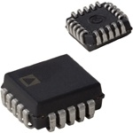
ICGOO电子元器件商城为您提供AD557JPZ由Analog设计生产,在icgoo商城现货销售,并且可以通过原厂、代理商等渠道进行代购。 AD557JPZ价格参考。AnalogAD557JPZ封装/规格:数据采集 - 数模转换器, 8 位 数模转换器 1 20-PLCC(9x9)。您可以下载AD557JPZ参考资料、Datasheet数据手册功能说明书,资料中有AD557JPZ 详细功能的应用电路图电压和使用方法及教程。
AD557JPZ是Analog Devices Inc.(亚德诺半导体)生产的一款数模转换器(DAC),属于数据采集系统中的关键组件。它主要用于将数字信号转换为模拟信号,广泛应用于各种需要高精度、低功耗和小尺寸的场合。以下是AD557JPZ的一些典型应用场景:

1. 工业自动化与控制:在工业控制系统中,AD557JPZ可以用于将来自微控制器或处理器的数字输出转换为模拟电压或电流信号,以驱动执行器、传感器或其他模拟设备。例如,在温度控制、压力调节等应用中,DAC可以精确地生成所需的控制信号。

2. 医疗设备:医疗仪器如心电图机、血压计等需要高精度的模拟信号来确保测量结果的准确性。AD557JPZ能够提供稳定的模拟输出,适用于这些对精度要求较高的医疗设备。

3. 通信系统:在通信领域,DAC用于调制解调器、无线发射器等设备中,将数字信息转换为模拟波形进行传输。AD557JPZ的低功耗特性使其特别适合便携式或电池供电的通信设备。

4. 音频处理:音频设备如音响、耳机放大器等需要将数字音频信号转换为模拟音频信号。AD557JPZ可以用于这些应用,提供高质量的音频输出,同时保持较低的噪声水平。

5. 测试与测量仪器:示波器、信号发生器等测试设备依赖于DAC来生成标准的测试信号。AD557JPZ的高分辨率和线性度使其成为这类设备的理想选择。

6. 消费电子:智能手表、智能家居设备等消费电子产品中也经常使用DAC来实现人机交互功能,例如通过触摸屏反馈震动或声音提示。AD557JPZ的小尺寸和低功耗特点非常适合这些小型化的产品设计。

总之,AD557JPZ凭借其高性能、低功耗和紧凑的设计,适用于多种需要精确模拟信号输出的应用场景。
| 参数 | 数值 |
| 产品目录 | 集成电路 (IC)半导体 |
| 描述 | IC DAC 8BIT V-OUT 20-PLCC数模转换器- DAC IC MONO 8-BIT |
| 产品分类 | |
| 品牌 | Analog Devices |
| 产品手册 | |
| 产品图片 |
|
| rohs | 符合RoHS无铅 / 符合限制有害物质指令(RoHS)规范要求 |
| 产品系列 | 数据转换器IC,数模转换器- DAC,Analog Devices AD557JPZDACPORT® |
| 数据手册 | |
| 产品型号 | AD557JPZ |
| 产品培训模块 | http://www.digikey.cn/PTM/IndividualPTM.page?site=cn&lang=zhs&ptm=19145http://www.digikey.cn/PTM/IndividualPTM.page?site=cn&lang=zhs&ptm=18614http://www.digikey.cn/PTM/IndividualPTM.page?site=cn&lang=zhs&ptm=26125http://www.digikey.cn/PTM/IndividualPTM.page?site=cn&lang=zhs&ptm=26140http://www.digikey.cn/PTM/IndividualPTM.page?site=cn&lang=zhs&ptm=26150http://www.digikey.cn/PTM/IndividualPTM.page?site=cn&lang=zhs&ptm=26147 |
| 产品目录页面 | |
| 产品种类 | 数模转换器- DAC |
| 位数 | 8 |
| 供应商器件封装 | 20-PLCC(9x9) |
| 分辨率 | 8 bit |
| 包装 | 管件 |
| 商标 | Analog Devices |
| 安装类型 | 表面贴装 |
| 安装风格 | SMD/SMT |
| 封装 | Tube |
| 封装/外壳 | 20-LCC(J 形引线) |
| 封装/箱体 | PLCC-20 |
| 工作温度 | 0°C ~ 70°C |
| 工厂包装数量 | 49 |
| 建立时间 | 800ns |
| 接口类型 | Parallel |
| 数据接口 | 并联 |
| 最大功率耗散 | 125 mW |
| 最大工作温度 | + 70 C |
| 最小工作温度 | 0 C |
| 标准包装 | 49 |
| 电压参考 | Internal |
| 电压源 | 单电源 |
| 电源电压-最大 | 5.5 V |
| 电源电压-最小 | 4.5 V |
| 积分非线性 | 1 LSB |
| 稳定时间 | 800 ns |
| 系列 | AD557 |
| 结构 | R-2R |
| 转换器数 | 1 |
| 转换器数量 | 1 |
| 输出数和类型 | 1 电压,单极1 电压,双极 |
| 输出类型 | Voltage |
| 采样比 | 1.25 MSPs |
| 采样率(每秒) | 1.25M |


- 商务部:美国ITC正式对集成电路等产品启动337调查
- 曝三星4nm工艺存在良率问题 高通将骁龙8 Gen1或转产台积电
- 太阳诱电将投资9.5亿元在常州建新厂生产MLCC 预计2023年完工
- 英特尔发布欧洲新工厂建设计划 深化IDM 2.0 战略
- 台积电先进制程称霸业界 有大客户加持明年业绩稳了
- 达到5530亿美元!SIA预计今年全球半导体销售额将创下新高
- 英特尔拟将自动驾驶子公司Mobileye上市 估值或超500亿美元
- 三星加码芯片和SET,合并消费电子和移动部门,撤换高东真等 CEO
- 三星电子宣布重大人事变动 还合并消费电子和移动部门
- 海关总署:前11个月进口集成电路产品价值2.52万亿元 增长14.8%


PDF Datasheet 数据手册内容提取
None
AD557–SPECIFICATIONS (@ T = 25(cid:3)C, V = 5 V unless otherwise noted) A CC Model Min Typ Max Unit ABSOLUTE MAXIMUM RATINGS* RESOLUTION 8 Bits V to Ground . . . . . . . . . . . . . . . . . . . . . . . . . . . 0 V to 18 V RELATIVE ACCURACY CC 0°C to 70°C ±1/2 1 LSB Digital Inputs (Pins 1–10) . . . . . . . . . . . . . . . . . . .0 V to 7.0 V V . . . . . . . . . . . . . . . . . . . . . . . Indefinite Short to Ground OUTPUT OUT Momentary Short to V Ranges 0 to 2.56 V CC Current Source 5 mA Power Dissipation . . . . . . . . . . . . . . . . . . . . . . . . . . . .450 mW Sink Internal Passive Storage Temperature Range Pull-Down to Ground2 N/P (Plastic) Packages . . . . . . . . . . . . . . . .–25°C to +100°C OUTPUT SETTLING TIME3 0.8 1.5 µs Lead Temperature (Soldering, 10 sec) . . . . . . . . . . . . . 300°C FULL-SCALE ACCURACY4 Thermal Resistance @ 25°C ±1.5 ±2.5 LSB Junction to Ambient/Junction to Case T to T ±2.5 ±4.0 LSB MIN MAX N/P (Plastic) Packages . . . . . . . . . . . . . . . . . .140/55°C/W ZERO ERROR @ 25°C ±1 LSB *Stresses above those listed under Absolute Maximum Ratings may cause perma- T to T ±3 LSB nent damage to the device. This is a stress rating only; functional operation of the MIN MAX device at these or any other conditions above those indicated in the operational MONOTONICITY5 section of this specification is not implied. Exposure to absolute maximum rating T to T Guaranteed But Not Tested MIN MAX conditions for extended periods may affect device reliability. DIGITAL INPUTS T to T MIN MAX Input Current (cid:2)100 µA PIN CONFIGURATIONS Data Inputs, Voltage Bit On—Logic “1” 2.0 V DIP Bit On—Logic “0” 0 0.8 V Control Inputs, Voltage On—Logic “1” 2.0 V (LSB) BIT 8 1 16 VOUT On—Logic “0” 0 0.8 V BIT 7 2 15 VOUT SENSE A Input Capacitance 4 pF BIT 6 3 AD557 14 VOUT SENSE B TIMING6 t Strobe Pulsewidth 225 ns BIT 5 4 TOP VIEW 13 GND W (Not to Scale) T to T 300 ns BIT 4 5 12 GND MIN MAX tDH Data Hold Time 10 ns BIT 3 6 11 +VCC T to T 10 ns t DMIaNta SetuMpA XTime 225 ns BIT 2 7 10 CS DS TMIN to TMAX 300 ns (MSB) BIT 1 8 9 CE POWER SUPPLY Operating Voltage Range (V ) 2.56 Volt Range CC 4.5 5.5 V PLCC Current (I ) 15 25 mA CC Rejection Ratio 0.03 %/% E A PONOOPEWTREEASRT DINISGS TIPEAMTPIOERNA, TVUCCR =E R5 AVNGE 0 75 71025 m°CW BIT 7 BIT 8 (LSB) NC VOUT V SENSOUT 1Relative Accuracy is defined as the deviation of the code transition points from the 3 2 1 20 19 ideal transfer point on a straight line from the offset to the full scale of the device. 2PSaeses i“vMe epauslul-rdinogw nO frfesseits tEanrrcoer ”is o2n k tΩhe. AD558 data sheet. BBIITT 56 45 PIDINE N1TIFIER 1187 VGONUDT SENSE B 3Settling time is specified for a positive-going full-scale step to ±1/2 LSB. Negative- AD557 going steps to zero are slower, but can be improved with an external pull-down. NC 6 TOP VIEW 16 NC 4The full-scale output voltage is 2.55 V and is guaranteed with a 5 V supply. BIT 4 7 (Not to Scale) 15 GND 5A monotonic converter has a maximum differential linearity error of ±1 LSB. 6See Figure 7. BIT 3 8 14 +VCC Specifications shown in boldface are tested on all production units at electrical test. 9 10 11 12 13 Specifications subject to change without notice. T 2 T 1 NC CE CS BI BI B) S ORDERING GUIDE NC = NO CONNECT M ( Temperature Package Package Model Range Description Option AD557JN 0°C to 70°C Plastic DIP N-16 AD557JP 0°C to 70°C Plastic Leaded Chip Carrier P-20A –2– REV. B
AD557 CIRCUIT DESCRIPTION CONNECTING THE AD557 The AD557 consists of four major functional blocks fabricated The AD557 has been configured for low cost and ease of appli- on a single monolithic chip (see Figure 1). The main D/A con- cation. All reference, output amplifier and logic connections are verter section uses eight equally weighted laser-trimmed current made internally. In addition, all calibration trims are performed sources switched into a silicon-chromium thin-film R/2R resistor at the factory assuring specified accuracy without user trims. ladder network to give a direct but unbuffered 0 mV to 400mV The only connection decision to be made by the user is whether output range. The transistors that form the DAC switches are the output range desired is unipolar or bipolar. Clean circuit PNPs; this allows direct positive-voltage logic interface and a board layout is facilitated by isolating all digital bit inputs on zero-based output range. one side of the package; analog outputs are on the opposite side. CONTROL DIGITAL INPUT DATA (BUS) UNIPOLAR 0 V TO 2.56 V OUTPUT RANGE INPUTS BIT1 BIT8 Figure 2 shows the configuration for the 0 V to 2.56 V full- CS CE (MSB) (LSB) +VCC GND GND scale output range. Because of its precise factory calibration, the AD557 is intended to be operated without user trims for gain l2L CONTROL l2L LATCHES and offset; therefore, no provisions have been made for such user LOGIC trims. If a small increase in scale is required, however, it may be BAND-GAP OUTPUT accomplished by slightly altering the effective gain of the output REFERENCE 8-BIT VOLTAGE-SWITCHING AMP D-TO-A CONVERTER VOUT bouutfpfeurt. rAan rgees. iNstootre itnh aset rdieesc rweaitshin Vg OthUeT sScEalNe SbyE pwuitltli ningc ar eraessies ttohre CONTROL AMP in series with GND will not work properly due to the code- VOUT SENSE A dependent currents in GND. Adjusting offset by injecting dc at VOUT SENSE B GND is not recommended for the same reason. Figure 1.Functional Block Diagram OUTPUT AMP The high-speed output buffer amplifier is operated in the nonin- verting mode with gain determined by the user-connections 16 VOUT at the output range select pin. The gain-setting application 15 VOUT SENSE A resistors are thin film laser trimmed to match and track the DAC resistors and to assure precise initial calibration of the out- 14 VOUT SENSE B put range, 0V to 2.56V. The amplifier output stage is an 13 GND NPN transistor with passive pull-down for zero-based output capability with a single power supply. Figure 2.0 V to 2.56 V Output Range The internal precision voltage reference is of the patented band-gap type. This design produces a reference voltage of BIPOLAR –1.28 V TO +1.28 V OUTPUT RANGE 1.2V and thus, unlike 6.3V temperature-compensated Zeners, The AD557 was designed for operation from a single power may be operated from a single, low-voltage logic power supply. supply and is thus capable of providing only a unipolar 0 V to The microprocessor interface logic consists of an 8-bit data 2.56 V output range. If a negative supply is available, bipolar latch and control circuitry. Low power, small geometry and high output ranges may be achieved by suitable output offsetting and speed are advantages of the I2L design as applied to this section. scaling. Figure 3 shows how a ±1.28 V output range may be I2L is bipolar process compatible so that the performance of the achieved when a –5 V power supply is available. The offset is analog sections need not be compromised to provide on-chip provided by the AD589 precision 1.2 V reference which will logic capabilities. The control logic allows the latches to be operate from a 5 V supply. The AD711 output amplifier can operated from a decoded microprocessor address and write sig- provide the necessary ±1.28 V output swing from ±5 V supplies. nal. If the application does not involve a µP or data bus, wiring Coding is complementary offset binary. CS and CE to ground renders the latches “transparent” for direct DAC access. 5k(cid:4) Digital Input Code Output VOUT = 0V TO 2.56V +5V Binary Hexadecimal Decimal Voltage 5k(cid:4) AD711 0.01(cid:1)F AD557 0000 0000 00 0 0 4.53k(cid:4) VO 0000 0001 01 1 0.010 V BIPO5L00A(cid:4)R 0.01(cid:1)F +–11..2278 TO 0000 0010 02 2 0.020 V OFFSET 1.5k(cid:4) AD589 ADJUST 0000 1111 0F 15 0.150 V VIN –5V 0001 0000 10 16 0.160 V 0.01(cid:1)F –41.7.2kV(cid:4) INPUT CODE VOUT 0111 1111 7F 127 1.270 V 00000000 +1.28V 10000000 0V 1000 0000 80 128 1.280 V 11111111 –1.27V 1100 0000 C0 192 1.920 V –5V 1111 1111 FF 255 2.55 V Figure 3.Bipolar Operation of AD557 from ±5 V Supplies REV. B –3–
AD557 APPLICATIONS Timing and Control Grounding and Bypassing The AD557 has data input latches that simplify interface to 8- All precision converter products require careful application of and 16-bit data buses. These latches are controlled by Chip good grounding practices to maintain full rated performance. Enable (CE) and Chip Select (CS) inputs. CE and CS are inter- Because the AD557 is intended for application in microcom- nally “NORed” so that the latches transmit input data to the puter systems where digital noise is prevalent, special care must DAC section when both CE and CS are at Logic “0.” If the be taken to assure that its inherent precision is realized. application does not involve a data bus, a “00” condition allows for direct operation of the DAC. When either CE or CS go to The AD557 has two ground (common) pins; this minimizes Logic “1,” the input data is latched into the registers and held ground drops and noise in the analog signal path. Figure 4 until both CE and CS return to “0.” (Unused CE or CS inputs shows how the ground connections should be made. should be tied to ground.) The truth table is given in Table I. It is often advisable to maintain separate analog and digital The logic function is also shown in Figure 6. grounds throughout a complete system, tying them common in one place only. If the common tie-point is remote and acciden- VOUT tal disconnection of that one common tie-point occurs due to 7.5 card removal with power on, a large differential voltage between 5.0 the two commons could develop. To protect devices that inter- 2.5 face to both digital and analog parts of the system, such as the AD557, it is recommended that common ground tie-points 00H 80H FFH AD557 INPUT CODE should be provided at each such device. If only one system Figure 6.AD557 Input Code vs. Level Shifted Output in a ground can be connected directly to the AD557, it is recom- “False” Ground Configuration mended that analog common be selected. Table I. AD557 Control Logic Truth Table Latch OUTPUT AMP Input Data CE CS DAC Data Condition VOUT 16 0 0 0 0 “Transparent” 15 VOUT SENSE A 1 0 0 1 “Transparent” VOUT SENSE B 0 g 0 0 Latching 14 RL 1 g 0 1 Latching 13 GND 0 0 g 0 Latching TO SYSTEM GND 1 0 g 1 Latching 12 GND 0.1(cid:1)F T(SOE SEY TSETXETM) GND X 1 X Previous Data Latched X X 1 Previous Data Latched 11 +VCC TO SYSTEM VCC NOTES Figure 4.Recommended Grounding and Bypassing X = Does not matter g = Logic Threshold at Positive-Going Transition Using a “False” Ground In a level-triggered latch such as that used in the AD557, there Many applications, such as disk drives, require servo control is an interaction between the data setup and hold times and voltages that swing on either side of a “false” ground. This the width of the enable pulse. In an effort to reduce the time ground is usually created by dividing the 12 V supply equally required to test all possible combinations in production, the and calling the midpoint voltage “ground.” AD557 is tested with t = t = 225 ns at 25°C and 300 ns at DS W T and T , with t = 10 ns at all temperatures. Failure to Figure 5 shows an easy and inexpensive way to implement this. MIN MAX DH comply with these specifications may result in data not being The AD586 is used to provide a stable 5 V reference from the latched properly. system’s 12 V supply. The op amp shown likewise operates from a single (12 V) supply available in the system. The resulting out- Figure 7 shows the timing for the data and control signals, CE put at the V node is ±2.5 V around the “false” ground point and CS are identical in timing as well as in function. OUT of 5 V. AD557 input code vs. V is shown in Figure 6. OUT t DH DATA t 2.0V INPUTS 0.8V DS 100k(cid:4) 200k(cid:4) AD557 2.0V 1/4 LM324 CS OR CE 0.8V t VOUT W 12V DAC 1/2 LSB 100k(cid:4) 6 2 V OUTPUT AD586 5V VIN 100k(cid:4) G“FRAOLUSNED” 4 tSETTLING tW = STROBE PULSEWIDTH = 225ns min Figure 5.Level Shifting the AD557 Output Around a ttDDHS == DDAATTAA SHEOTLUDP T TIMIMEE = = 1 202n5sn ms imnin “False” Ground tSETTLING = DAC SETTLING TIME TO (cid:2) 1/2 LSB Figure 7.AD557 Timing –4– REV. B
AD557 OUTLINE DIMENSIONS Dimensions shown in inches and (mm). N-16 (Plastic) Package 0.87 (22.1) MAX 0.25 0.31 (6.35) (7.87) 0.035 (0.59) 0.18 (4.57) MAX 0.18 0.125 0.011 (4.57) (3.18) MIN (0.28) 0.3 0.018 0.033 0.1 (7.62) (0.46) (0.84) (2.54) P-20A (PLCC) Package 0.173 (cid:2) 0.008 0.390 (cid:2) 0.005 (4.385 (cid:2) 0.185) (9.906 (cid:2) 0.125)SQ 0.105 (cid:2) 0.015 0.353 (cid:2) 0.003 (2.665 (cid:2) 0.375) (8.966 (cid:2) 0.076)SQ 0.020 (0.51) MIN 0.045 (cid:2) 0.003 (1.143 (cid:2) 0.076) 0.035 (cid:2) 0.01 (0.89 (cid:2) 0.25) NO.1 PIN IDENTIFIER 0.029 (cid:2) 0.003 (0.737 (cid:2) 0.076) TOP VIEW 0.017 (cid:2) 0.004 (0.432 (cid:2) 0.101) 0.020 (0.51) MAX 0.025 (0.64) MIN 0.02 (0.51) 0.050 MAX (1.27) 0.060 (1.53) MIN REV. B –5–
AD557–Revision History Location Page Data sheet changed from REV. A to REV. B. Changes to MONOTONICITY section of spec. page . . . . . . . . . 2 B) v. e r 1 ( 0 1/ – 0 – a 2 1 5 0 0 C A. S. U. N D I E T N RI P –6– REV. B