ICGOO在线商城 > 集成电路(IC) > 数据采集 - 数模转换器 > AD5680BRJZ-2REEL7
 Datasheet下载
- 型号: AD5680BRJZ-2REEL7
- 制造商: Analog
- 库位|库存: xxxx|xxxx
- 要求:
| 数量阶梯 | 香港交货 | 国内含税 |
| +xxxx | $xxxx | ¥xxxx |
查看当月历史价格
查看今年历史价格
AD5680BRJZ-2REEL7产品简介:
ICGOO电子元器件商城为您提供AD5680BRJZ-2REEL7由Analog设计生产,在icgoo商城现货销售,并且可以通过原厂、代理商等渠道进行代购。 AD5680BRJZ-2REEL7价格参考。AnalogAD5680BRJZ-2REEL7封装/规格:数据采集 - 数模转换器, 18 位 数模转换器 1 SOT-23-8。您可以下载AD5680BRJZ-2REEL7参考资料、Datasheet数据手册功能说明书,资料中有AD5680BRJZ-2REEL7 详细功能的应用电路图电压和使用方法及教程。
AD5680BRJZ-2REEL7 是由 Analog Devices Inc.(ADI)生产的一款高精度、低功耗的 16 位数模转换器(DAC),属于数据采集系统中的核心器件之一。以下是其主要应用场景:

 1. 工业自动化与控制
   - 过程控制:用于调节和控制工业设备中的温度、压力、流量等参数,通过将数字信号转换为模拟信号来驱动执行器或传感器。
   - 伺服电机控制:提供精确的电压输出以实现电机的速度和位置控制。
   - 可编程逻辑控制器 (PLC):作为 PLC 的一部分,用于生成模拟信号以驱动外部设备。

 2. 通信系统
   - 信号调制与解调:在通信领域中,用于生成复杂的波形信号,支持 AM、FM 或其他调制方式。
   - 射频 (RF) 应用:配合 RF 放大器使用,生成高频信号以满足无线通信需求。

 3. 测试与测量设备
   - 信号发生器:用于生成高精度的正弦波、方波或其他波形信号,适用于实验室或生产线测试。
   - 示波器校准:提供稳定的参考电压,确保测量设备的准确性。

 4. 医疗设备
   - 患者监护仪:用于生成精确的模拟信号,驱动显示屏或传感器接口。
   - 超声成像:参与超声波发射电路的设计,生成精确的激励信号。

 5. 消费电子
   - 音频处理:在高端音响设备中,用于将数字音频信号转换为模拟信号以驱动扬声器。
   - 触觉反馈:生成精确的电压信号以控制振动马达或力反馈装置。

 6. 汽车电子
   - 车载信息娱乐系统:用于音频信号的数模转换。
   - 自动驾驶系统:生成精确的控制信号以驱动传感器或执行器。

 特性总结
AD5680BRJZ-2REEL7 具有以下关键特性,使其适用于上述场景:
- 16 位分辨率:提供高精度的信号转换能力。
- 低功耗设计:适合对能效要求较高的应用。
- 小型封装:便于集成到紧凑型设计中。
- 宽工作电压范围:支持多种电源环境。

综上所述,AD5680BRJZ-2REEL7 广泛应用于需要高精度、低功耗和稳定性能的各类系统中,是现代电子设备中不可或缺的关键组件。
| 参数 | 数值 |
| 产品目录 | 集成电路 (IC) |
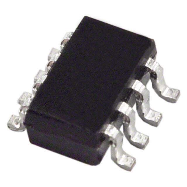
| 描述 | IC DAC 18BIT 5V SOT23-8 |
| 产品分类 | |
| 品牌 | Analog Devices Inc |
| 数据手册 | |
| 产品图片 |
|
| 产品型号 | AD5680BRJZ-2REEL7 |
| rohs | 无铅 / 符合限制有害物质指令(RoHS)规范要求 |
| 产品系列 | nanoDAC™ |
| 产品培训模块 | http://www.digikey.cn/PTM/IndividualPTM.page?site=cn&lang=zhs&ptm=19145http://www.digikey.cn/PTM/IndividualPTM.page?site=cn&lang=zhs&ptm=18614http://www.digikey.cn/PTM/IndividualPTM.page?site=cn&lang=zhs&ptm=26125http://www.digikey.cn/PTM/IndividualPTM.page?site=cn&lang=zhs&ptm=26140http://www.digikey.cn/PTM/IndividualPTM.page?site=cn&lang=zhs&ptm=26150http://www.digikey.cn/PTM/IndividualPTM.page?site=cn&lang=zhs&ptm=26147 |
| 产品目录页面 | |
| 位数 | 18 |
| 供应商器件封装 | SOT-23-8 |
| 其它名称 | AD5680BRJZ-2REEL7DKR |
| 包装 | Digi-Reel® |
| 安装类型 | 表面贴装 |
| 封装/外壳 | SOT-23-8 |
| 工作温度 | -40°C ~ 105°C |
| 建立时间 | 80µs |
| 数据接口 | DSP,MICROWIRE™,QSPI™,串行,SPI™ |
| 标准包装 | 1 |
| 特色产品 | http://www.digikey.cn/product-highlights/zh/analog-devices-ad568x-and-ad569x-nanodac/52095http://www.digikey.cn/product-highlights/cn/zh/analog-devices-select-q2-2014-products/4186 |
| 电压源 | 单电源 |
| 转换器数 | 1 |
| 输出数和类型 | 1 电压,单极 |
| 配用 | /product-detail/zh/EVAL-AD5680EBZ/EVAL-AD5680EBZ-ND/1825563 |
| 采样率(每秒) | - |


- 商务部:美国ITC正式对集成电路等产品启动337调查
- 曝三星4nm工艺存在良率问题 高通将骁龙8 Gen1或转产台积电
- 太阳诱电将投资9.5亿元在常州建新厂生产MLCC 预计2023年完工
- 英特尔发布欧洲新工厂建设计划 深化IDM 2.0 战略
- 台积电先进制程称霸业界 有大客户加持明年业绩稳了
- 达到5530亿美元!SIA预计今年全球半导体销售额将创下新高
- 英特尔拟将自动驾驶子公司Mobileye上市 估值或超500亿美元
- 三星加码芯片和SET,合并消费电子和移动部门,撤换高东真等 CEO
- 三星电子宣布重大人事变动 还合并消费电子和移动部门
- 海关总署:前11个月进口集成电路产品价值2.52万亿元 增长14.8%


PDF Datasheet 数据手册内容提取
5 V 18-Bit nanoDAC® in a SOT-23 Data Sheet AD5680 FEATURES FUNCTIONAL BLOCK DIAGRAM Single 18-bit nanoDAC VREF GND VDD 18-bit monotonic 12-bit accuracy guaranteed POWER-ON VFB RESET Tiny 8-lead SOT-23 package Power-on reset to zero scale/midscale REF(+) OBUUFTFPEURT VOUT DAC 4.5 V to 5.5 V power supply REGISTER 18-BIT DAC Serial interface Rail-to-rail operation SYNC interrupt facility INPUT CONTROL Temperature range: −40°C to +105°C LOGIC APPLICATIONS AD5680 CLolows ebda-nlodowpid ptrho dceastas caocqnutrioslit ion systems SYNC SCLK DIN 05854-001 Portable battery-powered instruments Figure 1. Gain and offset adjustment Precision setpoint control GENERAL DESCRIPTION The AD5680, a member of the nanoDAC family, is a single, The AD5680 uses a versatile 3-wire serial interface that operates 18-bit buffered voltage-out digital-to-analog converter (DAC) at clock rates up to 30 MHz, and is compatible with standard that operates from a single 4.5 V to 5.5 V supply and is 18-bit SPI®, QSPI™, MICROWIRE™, and DSP interface standards. monotonic. PRODUCT HIGHLIGHTS The AD5680 requires an external reference voltage to set the 1. 18 bits of resolution. output range of the DAC. The part incorporates a power-on 2. 12-bit accuracy guaranteed for 18-bit DAC. reset circuit that ensures the DAC output powers up to 0 V (AD5680-1) or to midscale (AD5680-2) and remains there until 3. Available in an 8-lead SOT-23. a valid write takes place. 4. Low power; typically consumes 1.6 mW at 5 V. The low power consumption of this part in normal operation 5. Power-on reset to zero scale or to midscale. makes it ideally suited to portable battery-operated equipment. RELATED DEVICES The power consumption is 1.6 mW at 5 V. AD5662—16-bit DAC in SOT-23. The AD5680 on-chip precision output amplifier allows rail-to- rail output swing to be achieved. For remote sensing applications, the output amplifier’s inverting input is available to the user. Rev. C Document Feedback Information furnished by Analog Devices is believed to be accurate and reliable. However, no responsibility is assumed by Analog Devices for its use, nor for any infringements of patents or other One Technology Way, P.O. Box 9106, Norwood, MA 02062-9106, U.S.A. rights of third parties that may result from its use. Specifications subject to change without notice. No license is granted by implication or otherwise under any patent or patent rights of Analog Devices. Tel: 781.329.4700©2006–2017 Analog Devices, Inc. All rights reserved. Trademarks and registered trademarks are the property of their respective owners. Technical Support www.analog.com
AD5680 Data Sheet TABLE OF CONTENTS Features .............................................................................................. 1 Output Amplifier ........................................................................ 11 Applications ....................................................................................... 1 Interpolator Architecture .......................................................... 11 Functional Block Diagram .............................................................. 1 Serial Interface ............................................................................ 12 General Description ......................................................................... 1 Input Shift Register .................................................................... 12 Product Highlights ........................................................................... 1 SYNC Interrupt .......................................................................... 12 Related Devices ................................................................................. 1 Power-On Reset .......................................................................... 12 Revision History ............................................................................... 2 Microprocessor Interfacing ....................................................... 13 Specifications ..................................................................................... 3 Applications Information .............................................................. 14 Timing Characteristics ................................................................ 4 Closed-Loop Applications ........................................................ 14 Absolute Maximum Ratings ............................................................ 5 Filter ............................................................................................. 14 ESD Caution .................................................................................. 5 Choosing a Reference for the AD5680 .................................... 15 Pin Configurations and Function Descriptions ........................... 6 Using a Reference as a Power Supply for the AD5680 .......... 16 Typical Performance Characteristics ............................................. 7 Using the AD5680 with a Galvanically Isolated Interface .... 16 Terminology .................................................................................... 10 Power Supply Bypassing and Grounding ................................ 16 Theory of Operation ...................................................................... 11 Outline Dimensions ....................................................................... 17 DAC Section ................................................................................ 11 Ordering Guide .......................................................................... 17 Resistor String ............................................................................. 11 REVISION HISTORY 7/2017—Rev. B to Rev. C Changed ADSP-BF53x to ADSP-BF531 ..................... Throughout Changed ADuM13x to ADuM130D ........................... Throughout Added t Parameter, Table 2 .................................................... 4 UPDATE Change to Figure 28 ....................................................................... 13 Changes to Figure 37 ...................................................................... 16 Changes to Ordering Guide .......................................................... 19 2/2014—Rev. A to Rev. B Added 8-Lead LFCSP ......................................................... Universal Changes to Figure 3 Caption and Table 4 Caption ...................... 6 Added Figure 4; Renumbered Sequentially .................................. 6 Updated Outline Dimensions ....................................................... 17 Changes to Ordering Guide .......................................................... 17 3/2007—Rev. 0 to Rev. A Changes to Input Shift Register Section ...................................... 12 Changes to Figure 25 ...................................................................... 12 6/2006—Revision 0: Initial Version Rev. C | Page 2 of 20
Data Sheet AD5680 SPECIFICATIONS V = 4.5 V to 5.5 V; R = 2 kΩ to GND; C = 200 pF to GND; V = V ; all specifications T to T , unless otherwise noted. DD L L REF DD MIN MAX Table 1. B Grade1 Parameter Min Typ Max Unit Conditions/Comments STATIC PERFORMANCE2 Resolution 18 Bits Relative Accuracy ±32 ±64 LSB Differential Nonlinearity3 ±1 LSB Measured in 50 Hz system bandwidth ±2 LSB Measured in 300 Hz system bandwidth Zero-Code Error 2 10 mV All 0s loaded to DAC register Full-Scale Error −0.2 −1 % FSR All 1s loaded to DAC register Offset Error ±10 mV Gain Error ±1.5 % FSR Zero-Code Error Drift ±2 μV/°C Gain Temperature Coefficient ±2.5 ppm Of FSR/°C DC Power Supply Rejection Ratio −100 dB DAC code = midscale; V = 5 V ± 10% DD OUTPUT CHARACTERISTICS3 Output Voltage Range 0 V V DD Output Voltage Settling Time 80 85 μs ¼ to ¾ scale change settling to ±8 LSB, R = 2 kΩ; 0 pF < C < 200 pF L L Slew Rate 1.5 V/μs ¼ to ¾ scale Capacitive Load Stability 2 nF R = ∞ L 10 nF R = 2 kΩ L Output Noise Spectral Density4 80 nV/√Hz DAC code = midscale, 10 kHz Output Noise (0.1 Hz to 10 Hz)4 25 μV p-p DAC code = midscale Total Harmonic Distortion (THD)4 −80 dB V = 2 V ± 300 mV p-p, f = 200 Hz REF Digital-to-Analog Glitch Impulse 5 nV-s 1 LSB change around major carry Digital Feedthrough 0.2 nV-s DC Output Impedance 0.5 Ω Short-Circuit Current4 30 mA V = 5 V DD REFERENCE INPUT Reference Current 40 75 μA V = V = 5 V REF DD Reference Input Range5 0.75 V V DD Reference Input Impedance 125 kΩ LOGIC INPUTS3 Input Current ±2 μA All digital inputs V , Input Low Voltage 0.8 V V = 5 V INL DD V , Input High Voltage 2 V V = 5 V INH DD Pin Capacitance 3 pF POWER REQUIREMENTS V 4.5 5.5 V All digital inputs at 0 V or V DD DD I (Normal Mode) DAC active and excluding load current DD V = 4.5 V to 5.5 V 325 450 μA V = V and V = GND DD IH DD IL POWER EFFICIENCY I /I 85 % I = 2 mA, V = 5 V OUT DD LOAD DD 1 Temperature range for B version is −40°C to +105°C, typical at +25°C. 2 DC specifications tested with the outputs unloaded, unless otherwise stated. Linearity calculated using a reduced code range of 2048 to 260,096. 3 Guaranteed by design and characterization; not production tested. 4 Output unloaded. 5 Reference input range at ambient where maximum DNL specification is achievable. Rev. C | Page 3 of 20
AD5680 Data Sheet TIMING CHARACTERISTICS All input signals are specified with t = t = 1 ns/V (10% to 90% of V ) and timed from a voltage level of (V + V )/2. See Figure 2. R F DD IL IH V = 4.5 V to 5.5 V; all specifications T to T , unless otherwise noted. DD MIN MAX Table 2. Limit at T , T MIN MAX Parameter V = 4.5 V to 5.5 V Unit Conditions/Comments DD t1 33 ns min SCLK cycle time 1 t 13 ns min SCLK high time 2 t 13 ns min SCLK low time 3 t 13 ns min SYNC to SCLK falling edge setup time 4 t 5 ns min Data setup time 5 t 4.5 ns min Data hold time 6 t 0 ns min SCLK falling edge to SYNC rising edge 7 t 33 ns min Minimum SYNC high time 8 t 13 ns min SYNC rising edge to SCLK fall ignore 9 t 0 ns min SCLK falling edge to SYNC fall ignore 10 t 250 μs min Minimum update period UPDATE 1 Maximum SCLK frequency is 30 MHz at VDD = 4.5 V to 5.5 V. t10 t1 t 9 SCLK t8 t4 t3 t2 t7 SYNC t 6 t DIN DB23 5 DB0 05854-002 Figure 2. Serial Write Operation Rev. C | Page 4 of 20
Data Sheet AD5680 ABSOLUTE MAXIMUM RATINGS T = 25°C, unless otherwise noted. A Stresses at or above those listed under Absolute Maximum Ratings may cause permanent damage to the product. This is a Table 3. stress rating only; functional operation of the product at these Parameter Rating or any other conditions above those indicated in the operational V to GND −0.3 V to +7 V DD section of this specification is not implied. Operation beyond V to GND −0.3 V to V + 0.3 V OUT DD the maximum operating conditions for extended periods may V to GND −0.3 V to V + 0.3 V FB DD affect product reliability. V to GND −0.3 V to V + 0.3 V REF DD Digital Input Voltage to GND −0.3 V to V + 0.3 V DD Operating Temperature Range ESD CAUTION Industrial (B Version) −40°C to +105°C Storage Temperature Range −65°C to +150°C Junction Temperature (T max) 150°C J Power Dissipation (T max − T )/θ J A JA θJA Thermal Impedance SOT-23 Package (4-Layer Board) 119°C/W Reflow Soldering Peak Temperature Pb-free 260°C Rev. C | Page 5 of 20
AD5680 Data Sheet PIN CONFIGURATIONS AND FUNCTION DESCRIPTIONS VDD 1 8 GND VREF 2 AD5680 7 DIN VDD 1 8 GND VFB 3 (NToOt Pto V SIEcWale) 6 SCLK VREF 2 ATODP5 V6IE8W0 7 DIN VOUT 4 5 SYNC 05854-003 VVOFUBT 34 (Not to Scale) 65 SSCYNLKC 05854-104 Figure 3. 8-Lead SOT-23 Pin Configuration Figure 4. 8-Lead LFCSP Pin Configuration Table 4. 8-Lead SOT-23 and 8-Lead LFSCP Pin Function Descriptions Pin No. Mnemonic Description 1 V Power Supply Input. The part can be operated from 4.5 V to 5.5 V. V should be decoupled to GND. DD DD 2 V Reference Voltage Input. REF 3 V Feedback Connection for the Output Amplifier. V should be connected to V for normal operation. FB FB OUT 4 V Analog Output Voltage from DAC. The output amplifier has rail-to-rail operation. OUT 5 SYNC Level-Triggered Control Input (Active Low). This is the frame synchronization signal for the input data. When SYNC goes low, it enables the input shift register and data is transferred in on the falling edges of the following clocks. The DAC is updated following the 24th clock cycle unless SYNC is taken high before this edge, in which case the rising edge of SYNC acts as an interrupt and the write sequence is ignored by the DAC. SYNC 6 SCLK Serial Clock Input. Data is clocked into the input shift register on the falling edge of the serial clock input. Data can be transferred at rates up to 30 MHz. 7 DIN Serial Data Input. This device has a 24-bit shift register. Data is clocked into the register on the falling edge of the serial clock input. 8 GND Ground. Ground reference point for all circuitry on the part. Rev. C | Page 6 of 20
Data Sheet AD5680 TYPICAL PERFORMANCE CHARACTERISTICS 40 0 VDD = VREF = 5V VDD = 5V 32 TA = 25°C –0.02 24 –0.04 GAIN ERROR 16 –0.06 R (LSB) 8 % FSR) –0.08 RO 0 R ( –0.10 R O L E –8 RR –0.12 N E I –16 –0.14 FULL-SCALE ERROR –24 –0.16 ––4302 05854-028 ––00..1280 05854-044 0 40k 80k 120k 160k 200k 240k –40 –20 0 20 40 60 80 100 CODE TEMPERATURE (C) Figure 5. Typical INL Plot Figure 8. Gain Error and Full-Scale Error vs. Temperature 1.0 1.5 VDD = VREF = 5V 0.8 TA = 25°C 1.0 ZERO-SCALE ERROR 0.6 0.5 0.4 B) LS 0.2 V) 0 ROR ( 0 OR (m –0.5 R R L E –0.2 ER –1.0 N D –0.4 –1.5 –0.6 OFFSET ERROR ––10..08 05854-029 ––22..05 05854-043 0 25k 50k 75k 100k 125k 150k 175k 200k 225k 250k –40 –20 0 20 40 60 80 100 CODE TEMPERATURE (C) Figure 6. Typical DNL Plot in 50 Hz System Bandwidth Figure 9. Zero-Scale Error and Offset Error vs. Temperature ±4 0.20 VT D=D – =4 04°.C5V T TOO + 51.055V°C 0.15 VTAD D= =2 5V°RCEF= 5V, 3V DZSEIANRCKO ILN OSGCA CADULEERD R –WEINTTH 0.10 ±2 E (V) 0.05 )SB TAG 0 L L DN( L OR VO –0.05 ±1 RR –0.10 E –0.15 DAC LOADED WITH 0 0 SY5S0TEM BANDWIDTH 3(0H0z) >300 05854-042 ––00..2250–5 –4 –FS3UOLULR CS–2CINAGL EC– U1–RRI E(mN0AT) 1 2 3 4 505854-014 Figure 7. DNL Performance vs. System Bandwidth Figure 10. Headroom at Rails vs. Source and Sink Current Rev. C | Page 7 of 20
AD5680 Data Sheet 450 VDD = VREF = 5V 400 TA = 25°C SCLK 350 1 300 DIN A) 250 (µDD 200 2 I ∆: 1.52V 150 ∆: 64.8µs @: 1.20V VOUT 100 5000 4000 8000 120C0O0DE 16000 20000 24000 05854-007 3 CCHH13 21..0000VV CH2 2.00V M 20.0µs CH4 1.30V 05854-015 Figure 11. Supply Current vs. Code Figure 14. Full-Scale Settling Time, 5 V 350 VDD = VREF = 5V 300 VDD 1 250 (µA)D 200 2 VREF VCO3 UMTAX ID 150 284mV VOUT 100 C3 MIN –52mV 50 VOUT 0–40 –20 0 TEM2P0ERATU4R0E (°C)60 80 100 05854-006 3 CCHH13 31.0000mVV CH2 3.00V M 100µs CH1 2.40V 05854-016 Figure 12. Supply Current vs. Temperature Figure 15. Power-On Reset to 0 V 700 TA = 25°C 600 VDD = 5V VDD 1 500 2 µA) 400 VREF VOUT (D C3 MAX ID 300 2.5V VOUT 200 C3 MIN –40mV 100 VOUT 00 1 2VLOGIC (V)3 4 5 05854-004 3 CCHH13 35.0000mVV CH2 3.00V M 100µs CH1 2.40V 05854-017 Figure 13. Supply Current vs. Logic Input Voltage Figure 16. Power-On Reset to Midscale Rev. C | Page 8 of 20
Data Sheet AD5680 2.502500 16 22..550022205000 VT13ADn D=s =/2S 5VA°RCMEPF L=E 5 NVUMBER 14 VTAR E=F 2=5 °VCDD 2.501750 1 LSB CHANGEAROUND MIDSCALE (0x20000TO0x1FFFF) 2.501500 GLITCH IMPULSE = 2.723nV-s VDD=3V 2.501250 12 DE2.501000 s) MPLITU22..550000755000 TIME (µ 10 A2.500250 2.500000 8 VDD=5V 2.499750 2.499500 6 222...444999998207505000 05854-005 4 05854-027 0 50 100 150 200 250 300 350 400 450 500 550 0 1 2 3 4 5 6 7 8 9 10 SAMPLE NUMBER CAPACITANCE (nF) Figure 17. Digital-to-Analog Glitch Impulse (Negative) Figure 20. Settling Time vs. Capacitive Load 2.5010 VDD = VREF = 5V VDD= VREF = 5V 2.5008 TA = 25°C TA = 25°C DAC LOADED WITH MIDSCALE DAC LOADED WITH MIDSCALE 2.5006 DIGITAL FEEDTHROUGH = 0.201nV 2.5004 2.5002 MPLITUDE222...445990990680 5µV/DIV 1 VREF A 2.4994 2.4992 2.4990 22..44998868 05854-020 05854-019 0 50 100 150 200 250 300 350 400 450 500 5s/DIV SAMPLES×6.5ns Figure 18. Digital Feedthrough Figure 21. 0.1 Hz to 10 Hz Output Noise Plot –20 1000 VDD = 5V VDD = VREF = 5V TA = 25°C 900 TA = 25°C –30 FULL SCALE LOADED MIDSCALE LOADED VREF = 2V ±300mV p-p 800 –40 700 –50 Hz) 600 (dB) –60 E (nV/ 500 S –70 NOI 400 300 –80 200 –1–0900 05854-018 1000 05854-013 0 1 2 3 4 5 6 7 8 9 10 100 1k 10k 100k 1M FREQUENCY (kHz) FREQUENCY (Hz) Figure 19. Total Harmonic Distortion Figure 22. Noise Spectral Density Rev. C | Page 9 of 20
AD5680 Data Sheet TERMINOLOGY Relative Accuracy or Integral Nonlinearity (INL) DC Power Supply Rejection Ratio (PSRR) For the DAC, relative accuracy or integral nonlinearity is a This indicates how the output of the DAC is affected by changes measurement of the maximum deviation, in LSBs, from a in the supply voltage. PSRR is the ratio of the change in V to OUT straight line passing through the endpoints of the DAC transfer a change in V for full-scale output of the DAC. It is measured DD function. Figure 5 shows a typical INL vs. code plot. in dB. V is held at 2 V, and V is varied by ±10%. REF DD Differential Nonlinearity (DNL) Output Voltage Settling Time Differential nonlinearity is the difference between the measured This is the amount of time it takes for the output of a DAC to change and the ideal 1 LSB change between any two adjacent settle to a specified level for a ¼ to ¾ full-scale input change codes. A specified differential nonlinearity of ±1 LSB maximum and is measured from the 24th falling edge of SCLK. ensures monotonicity. Figure 6 shows a typical DNL vs. code Digital-to-Analog Glitch Impulse plot. Digital-to-analog glitch impulse is injected into the analog Zero-Code Error output when the input code in the DAC register changes state. Zero-code error is a measurement of the output error when It is normally specified as the area of the glitch in nV-s, and is zero code (0x00000) is loaded to the DAC register. Ideally, the measured when the digital input code is changed by 1 LSB at output should be 0 V. The zero-code error is always positive in the major carry transition (0x1FFFF to 0x20000). See Figure 17. the AD5680 because the output of the DAC cannot go below Digital Feedthrough 0 V. It is due to a combination of the offset errors in the DAC Digital feedthrough is a measure of the impulse injected into and the output amplifier. Zero-code error is expressed in mV. A the analog output of the DAC from the digital inputs of the plot of zero-code error vs. temperature can be seen in Figure 9. DAC, but is measured when the DAC output is not updated. It Full-Scale Error is specified in nV-s and measured with a full-scale code change Full-scale error is a measurement of the output error when full- on the data bus, that is, from all 0s to all 1s and vice versa. scale code (0x3FFFF) is loaded to the DAC register. Ideally, the Total Harmonic Distortion (THD) output should be V − 1 LSB. Full-scale error is expressed in DD This is the difference between an ideal sine wave and its percent of full-scale range. attenuated version using the DAC. The sine wave is used as the Gain Error reference for the DAC. The THD is a measurement of the This is a measure of the span error of the DAC. It is the deviation harmonics present on the DAC output. It is measured in dB. in slope of the DAC transfer characteristic from ideal, expressed Noise Spectral Density as a percent of the full-scale range. This is a measurement of the internally generated random Zero-Code Error Drift noise. Random noise is characterized as a spectral density This is a measurement of the change in zero-code error with a (voltage per √Hz). It is measured by loading the DAC to change in temperature. It is expressed in µV/°C. midscale and measuring noise at the output. It is measured in nV/√Hz. Figure 22 shows a plot of noise spectral density. Gain Temperature Coefficient This is a measurement of the change in gain error with a change in temperature. It is expressed in (ppm of full-scale range)/°C. Offset Error Offset error is a measure of the difference between V (actual) OUT and V (ideal), expressed in mV in the linear region of the OUT transfer function. Offset error is measured on the AD5680 with Code 2048 loaded in the DAC register. It can be negative or positive. Rev. C | Page 10 of 20
Data Sheet AD5680 THEORY OF OPERATION DAC SECTION OUTPUT AMPLIFIER The AD5680 DAC is fabricated on a CMOS process. The The output buffer amplifier can generate rail-to-rail voltages on architecture consists of a string DAC followed by an output its output, which gives an output range of 0 V to V . This output DD buffer amplifier. Figure 23 shows a block diagram of the DAC buffer amplifier has a gain of 2 derived from a 50 kΩ resistor architecture. divider network in the feedback path. The output amplifier’s VDD R inverting input is available to the user, allowing for remote VFB sensing. This VFB pin must be connected to VOUT for normal REF (+) R operation. It can drive a load of 2 kΩ in parallel with 1000 pF to DAC REGISTER RSETSRISINTOGR VOUT GND. The source and sink capabilities of the output amplifier can be seen in Figure 10. The slew rate is 1.5 V/μs with a ¼ to ¾ REF (–) OUTPUT full-scale settling time of 10 μs. GND AMPLIFIER 05854-030 INTERPOLATOR ARCHITECTURE Figure 23. DAC Architecture The AD5680 contains a 16-bit DAC with an internal clock Because the input coding to the DAC is straight binary, the ideal generator and interpolator. The voltage levels generated by the output voltage is given by 16-bit, 1 LSB step can be subdivided using the interpolator to increase the resolution to 18 bits. D VOUT VREF The 18-bit input code can be divided into two segments: 262,144 16-bit DAC code (DB19 to DB4) and 2-bit interpolator code where D is the decimal equivalent of the binary code that is (DB3 and DB2). The input to the DAC is switched between a loaded to the DAC register. It can range from 0 to 262,143. 16-bit code (for example, Code 1023) and a 16-bit code + 1 LSB RESISTOR STRING (for example, Code 1024). The 2-bit interpolator code deter- mines the duty cycle of the switching and hence the 18-bit The resistor string section is shown in Figure 24. It is simply a code level. See Table 5 for an example. string of resistors, each of value R. The code loaded to the DAC register determines at which node on the string the voltage is Table 5. tapped off to be fed into the output amplifier. The voltage is 16-Bit 2-Bit tapped off by closing one of the switches connecting the string 18-Bit Code DAC Code Interpolator Code Duty to the amplifier. Because it is a string of resistors, it is guaranteed DB19 to DB2 DB19 to DB4 DB3 DB2 Cycle monotonic. 4092 1023 0 0 0 4093 1023 0 1 25% 4094 1023 1 0 50% R 4095 1023 1 1 75% 4096 1024 0 0 0 R The DAC output voltage is given by the average value of the waveform switching between 16-bit code (C) and 16-bit R TO OUTPUT AMPLIFIER code + 1 (C + 1). The output voltage is a function of the duty cycle of the switching. FILTER 18-BIT INPUT CODE PLANT C MUX DAC 18 16C + 1 16 VOUT +1 C + 1 R C 75% DUTY CYCLE C + 1 50% DUTY CYCLE INTERPOLATOR C 2 C + 1 R 05854-031 CLKFigure 25. InterpolaCtion Architecture 25% DUTY CYCLE05854-032 Figure 24. Resistor String Rev. C | Page 11 of 20
AD5680 Data Sheet SERIAL INTERFACE INPUT SHIFT REGISTER The AD5680 has a 3-wire serial interface (SYNC, SCLK, and The input shift register is 24 bits wide (see Figure 26). The first DIN) that is compatible with SPI, QSPI, and MICROWIRE two bits are don’t care bits. Bit DB21 and Bit DB20 are reserved interface standards as well as with most DSPs. See Figure 2 for bits and should be set to 0. The next 18 bits are the data bits a timing diagram of a typical write sequence. followed by two don’t care bits. These are transferred to the DAC register on the 24th falling edge of SCLK. The write sequence begins by bringing the SYNC line low. Data SYNC INTERRUPT from the DIN line is clocked into the 24-bit shift register on the falling edge of SCLK. The serial clock frequency can be as high In a normal write sequence, the SYNC line is kept low for at as 30 MHz, making the AD5680 compatible with high speed least 24 falling edges of SCLK, and the DAC is updated on the DSPs. On the 24th falling clock edge, the last data bit is clocked 24th falling edge. However, if SYNC is brought high before the in and the programmed function is executed, that is, a change 24th falling edge, this acts as an interrupt to the write sequence. in DAC register contents occurs. At this stage, the SYNC line The shift register is reset and the write sequence is seen as invalid. can be kept low or brought high. In either case, it must be Neither an update of the DAC register contents nor a change in brought high for a minimum of 33 ns before the next write the operating mode occurs (see Figure 27). sequence so that a falling edge of SYNC can initiate the next POWER-ON RESET write sequence. Because the SYNC buffer draws more current when VIN = 2 V than it does when VIN = 0.8 V, SYNC should be The AD5680 family contains a power-on reset circuit that controls the output voltage during power-up. The AD5680-1 idled low between write sequences for even lower power DAC output powers up to 0 V, and the AD5680-2 DAC output operation. As mentioned previously, it must, however, be brought high again just before the next write sequence. powers up to midscale. The output remains there until a valid write sequence is made to the DAC. This is useful in applications where it is important to know the output state of the DAC while it is in the process of powering up. DB23 (MSB) DB0 (LSB) X X 0 0 D17 D16 D15 D14 D13 D12 D11 D10 D9 D8 D7 D6 D5 D4 D3 D2 D1 D0 X X DATA BITS 05854-033 RESERVED BITS Figure 26. Input Register Contents SCLK SYNC DIN DB23 DB0 DB23 DB0 SYNC HINIGVAHL BIDE FWORRITEE 2 4STEHQFUAELNLICNEG: EDGE OUTPUT UPVDAALTIDE SW ORINT ET HSEE Q24UTEHNFCAEL:LING EDGE 05854-034 Figure 27. SYNC Interrupt Facility Rev. C | Page 12 of 20
Data Sheet AD5680 MICROPROCESSOR INTERFACING AD5680 to 80C51/80L51 Interface AD5680 to Blackfin® ADSP-BF531 Interface Figure 30 shows a serial interface between the AD5680 and the 80C51/80L51 microcontroller. The setup for the interface is as Figure 28 shows a serial interface between the AD5680 and follows. TxD of the 80C51/80L51 drives SCLK of the AD5680, the Blackfin ADSP-BF531 microprocessor. The ADSP-BF531 processor family incorporates two dual-channel synchronous while RxD drives the serial data line of the part. The SYNC serial ports, SPORT1 and SPORT0, for serial and multiprocessor signal is again derived from a bit-programmable pin on the port. communications. Using SPORT0 to connect to the AD5680, the In this case, port line P3.3 is used. When data is to be transmitted setup for the interface is as follows. DT0PRI drives the DIN pin to the AD5680, P3.3 is taken low. The 80C51/80L51 transmits of the AD5680, while TSCLK0 drives the SCLK of the part. The data in 8-bit bytes only; thus, only eight falling clock edges occur SYNC is driven from TFS0. in the transmit cycle. To load data to the DAC, P3.3 is left low after the first eight bits are transmitted, and a second write cycle ADSP-BF531* AD5680* is initiated to transmit the second byte of data. P3.3 is taken high following the completion of this cycle. The 80C51/80L51 outputs the serial data in a format that has the LSB first. The TFS0 SYNC AD5680 must receive data with the MSB first. The 80C51/80L51 DT0PRI DIN transmit routine should take this into account. TSCLK0 SCLK *ADDITIONAL PINS OMITTED FOR CLARITY. 05854-035 80C51/80L51* AD5680* Figure 28. AD5680 to Blackfin ADSP-BF531 Interface P3.3 SYNC AD5680 to 68HC11/68L11 Interface TxD SCLK F68igHuCre1 219/6 s8hLo1w1s m a iscerroicaol ninttreorlflaerc.e S bCeKtw oefe tnh teh 6e8 AHDC51618/608 aLn1d1 the RxD DIN 05854-037 drives the SCLK of the AD5680, while the MOSI output drives *ADDITIONAL PINS OMITTED FOR CLARITY. the serial data line of the DAC. Figure 30. AD5680 to 80C51/80L51 Interface The SYNC signal is derived from a port line (PC7). The setup AD5680 to MICROWIRE Interface conditions for correct operation of this interface are as follows: Figure 31 shows an interface between the AD5680 and any The 68HC11/68L11 is configured with its CPOL bit as 0 and its MICROWIRE-compatible device. Serial data is shifted out on CPHA bit as 1. When data is being transmitted to the DAC, the the falling edge of the serial clock and is clocked into the AD5680 SYNC line is taken low (PC7). When the 68HC11/68L11 is on the rising edge of the SK. configured this way, data appearing on the MOSI output is valid on the falling edge of SCK. Serial data from the 68HC11/68L11 MICROWIRE* AD5680* is transmitted in 8-bit bytes with only eight falling clock edges occurring in the transmit cycle. Data is transmitted MSB first. To CS SYNC load data to the AD5680, PC7 is left low after the first eight bits SK SCLK atore t htrea DnsAfeCrr; ePdC, 7a nisd t aa kseenco hnidg hs earti athl ew ernitde oopf ethraisti porno icse pdeurrfeo.r med SO DIN 05854-038 *ADDITIONAL PINS OMITTED FOR CLARITY. 68HC11/68L11* AD5680* Figure 31. AD5680 to MICROWIRE Interface PC7 SYNC SCK SCLK MOSI DIN 05854-036 *ADDITIONAL PINS OMITTED FOR CLARITY. Figure 29. AD5680 to 68HC11/68L11 Interface Rev. C | Page 13 of 20
AD5680 Data Sheet APPLICATIONS INFORMATION CLOSED-LOOP APPLICATIONS ∆: 2.09ms The AD5680 is suitable for closed-loop low bandwidth applica- @: 1.28ms 2 tions. Ideally, the system bandwidth acts as a filter on the DAC output. (See the Filter section for details of the DAC output prefiltering and postfiltering.) The DAC updates at the interpolation frequency of 10 kHz. 1 PLANT CONTROLLER DAC CODE 4092 CODE 4094 05854-025 ADC 05854-039 CH1Fig20u.r0eµ V34C. DH2A C5V Output wiMth 5 5000 µHsz Filter on OCuHt2p u t 1.4V Figure 32. Typical Closed-Loop Application FILTER ∆: 2.09ms @: 1.28ms The DAC output voltage for code transition 4092 to 4094 can be 2 seen in Figure 33. This is the DAC output unfiltered. Code 4092 does not have any interpolation but Code 4094 has interpolation with a 50% duty cycle (see Table 5). Figure 34 shows the DAC output with a 50 Hz passive RC filter and Figure 35 shows the output with a 300 Hz passive RC filter. An RC combination of 1 320 kΩ and 10 nF has been used to achieve the 50 Hz cutoff frequency, and an RC combination of 81 kΩ and 10 nF has been used to achieve the 300 Hz cutoff frequency. CODE 4092 CODE 4094 05854-026 CH1 20.0µV CH2 5V M 500µs CH2 1.4V Figure 35. DAC Output with 300 Hz Filter on Output CODE 4092 CODE 4094 1 05854-024 CH1 20.0µV M 500µs CH4 0V Figure 33. DAC Output Unfiltered Rev. C | Page 14 of 20
Data Sheet AD5680 CHOOSING A REFERENCE FOR THE AD5680 Long-term drift is a measurement of how much the reference drifts over time. A reference with a tight long-term drift speci- To achieve the optimum performance from the AD5680, choose fication ensures that the overall solution remains relatively stable a precision voltage reference carefully. The AD5680 has only during its entire lifetime. one reference input, V . The voltage on the reference input is REF used to supply the positive input to the DAC. Therefore, any The temperature coefficient of a reference’s output voltage error in the reference is reflected in the DAC. affects INL, DNL, and TUE. A reference with a tight temperature coefficient specification should be chosen to reduce temperature When choosing a voltage reference for high accuracy applica- dependence of the DAC output voltage in ambient conditions. tions, the sources of error are initial accuracy, ppm drift, long- term drift, and output voltage noise. Initial accuracy on the In high accuracy applications, which have a relatively low noise output voltage of the DAC leads to a full-scale error in the DAC. budget, reference output voltage noise needs to be considered. It To minimize these errors, a reference with high initial accuracy is important to choose a reference with as low an output noise is preferred. In addition, choosing a reference with an output voltage as is practical for the system noise resolution required. trim adjustment, such as the ADR425, allows a system designer Precision voltage references such as the ADR425 produce low to trim out system errors by setting a reference voltage to a output noise in the 0.1 Hz to 10 Hz range. Examples of recom- voltage other than the nominal. The trim adjustment can also mended precision references for use as supply to the AD5680 be used at temperature to trim out any error. are shown in the Table 6. Table 6. Partial List of Precision References for Use with the AD5680 Part No. Initial Accuracy (mV max) Temperature Drift (ppm/°C max) 0.1 Hz to 10 Hz Noise (μV p-p typ) V (V) OUT ADR425 ±2 3 3.4 5 ADR395 ±6 25 5 5 REF195 ±2 5 50 5 Rev. C | Page 15 of 20
AD5680 Data Sheet USING A REFERENCE AS A POWER SUPPLY FOR 5V THE AD5680 REGULATOR POWER 10µF 0.1µF Because the supply current required by the AD5680 is extremely low, an alternative option is to use a voltage reference to supply the required voltage to the part (see Figure 36). This is especially VDD useful if the power supply is quite noisy, or if the system supply SCLK VIA VOA SCLK voltages are at some value other than 5 V, for example, 15 V. ADuM130D AD5680 The voltage reference outputs a steady supply voltage for the AD5680; see Table 6 for a suitable reference. If the low dropout REF195 is used, it must supply 325 μA of current to the AD5680, SYNC VIB VOB SYNC VOUT with no load on the output of the DAC. When the DAC output is loaded, the REF195 also needs to supply the current to the load. The total current required (with a 5 kΩ load on the DAC output) is DIN VIC VOC DIN GND 325 μA + (5 V/5 kΩ) = 1.33 mA 05854-041 The load regulation of the REF195 is typically 2 ppm/mA, Figure 37. AD5680 with a Galvanically Isolated Interface which results in a 2.7 ppm (13.5 μV) error for the 1.33 mA POWER SUPPLY BYPASSING AND GROUNDING current drawn from it. This corresponds to a 0.177 LSB error. When accuracy is important in a circuit, it is helpful to carefully 15V consider the power supply and ground return layout on the board. 5V The printed circuit board containing the AD5680 should have REF195 250µA separate analog and digital sections, each having its own area of the board. If the AD5680 is in a system where other devices require an AGND-to-DGND connection, the connection should 3-WIRE SYNC VDD VREF VOUT = 0VTO 5V be made at one point only. This ground point should be as close SERIAL SCLK AD5680 INTERFACE as possible to the AD5680. DIN 05854-040 The power supply to the AD5680 should be bypassed with 10 μF Figure 36. REF195 as Power Supply to the AD5680 and 0.1 μF capacitors. The capacitors should be located as close USING THE AD5680 WITH A GALVANICALLY as possible to the device, with the 0.1 μF capacitor ideally right ISOLATED INTERFACE up against the device. The 10 μF capacitors should be the tanta- lum bead type. It is important that the 0.1 μF capacitor has low In process-control applications in industrial environments, it is effective series resistance (ESR) and effective series inductance often necessary to use a galvanically isolated interface to protect (ESI), for example, common ceramic types of capacitors. This and isolate the controlling circuitry from any hazardous common- 0.1 μF capacitor provides a low impedance path to ground for mode voltages that might occur in the area where the DAC is high frequencies caused by transient currents due to internal functioning. Isocouplers provide isolation in excess of 3 kV. The logic switching. AD5680 uses a 3-wire serial logic interface, so the ADuM130D The power supply line itself should have as large a trace as 3-channel digital isolator provides the required isolation (see possible to provide a low impedance path and to reduce glitch Figure 37). The power supply to the part also needs to be isolated, effects on the supply line. Clocks and other fast switching digital which is done by using a transformer. On the DAC side of the signals should be shielded from other parts of the board by transformer, a 5 V regulator provides the 5 V supply required digital ground. Avoid crossover of digital and analog signals if for the AD5680. possible. When traces cross on opposite sides of the board, ensure that they run at right angles to each other to reduce feedthrough effects on the board. The best board layout tech- nique is the microstrip technique where the component side of the board is dedicated to the ground plane only and the signal traces are placed on the solder side. However, this is not always possible with a 2-layer board. Rev. C | Page 16 of 20
Data Sheet AD5680 OUTLINE DIMENSIONS 3.00 2.90 2.80 1.70 8 7 6 5 3.00 1.60 2.80 1.50 2.60 1 2 3 4 PIN1 INDICATOR 0.65BSC 1.95 BSC 1.30 1.15 0.90 1.45MAX 0.22MAX 0.95MIN 0.08MIN 0.60 0.15MAX 8° 0.45 0.05MIN 0.38MAX SPLEAATNIENG 4° B0S.6C0 0.30 0.22MIN 0° COMPLIANTTOJEDECSTANDARDSMO-178-BA 12-16-2008-A Figure 38. 8-Lead Small Outline Transistor Package [SOT-23] (RJ-8) Dimensions shown in millimeters 3.10 1.95 REF 3.00 SQ 2.90 0.65 BSC 5 8 PIN 1 INDEX AREA 0.50 PIN 1 CORNER C 0.130× 45° 0.40 0.30 4 1 TOP VIEW BOTTOM VIEW 0.80 0.75 0.05 MAX 0.70 0.00 MIN COPLANARITY SEATING 0.35 0.08 PLANE 0.30 0.203 REF 0.C2O5MPLIANTTOJEDEC STANDARDS MO-229-WEEC-2 02-23-2011-A Figure 39. 8-Lead Lead Frame Chip Scale Package [LFCSP_WD] 3 mm × 3 mm Body, Very Very Thin, Dual Lead (CP-8-15) Dimensions shown in millimeters ORDERING GUIDE Power-On Package Package Model1 Reset to Code Accuracy Temperature Range Description Option Branding AD5680BRJZ-1500RL7 Zero ±64 LSB INL −40°C to +105°C 8-Lead SOT-23 RJ-8 D3C AD5680BRJZ-1REEL7 Zero ±64 LSB INL −40°C to +105°C 8-Lead SOT-23 RJ-8 D3C AD5680BRJZ-2500RL7 Midscale ±64 LSB INL −40°C to +105°C 8-Lead SOT-23 RJ-8 D3D AD5680BRJZ-2REEL7 Midscale ±64 LSB INL −40°C to +105°C 8-Lead SOT-23 RJ-8 D3D AD5680BCPZ-1500RL7 Zero ±64 LSB INL −40°C to +105°C 8-Lead LFCSP CP-8-15 DLN AD5680BCPZ-1RL7 Zero ±64 LSB INL −40°C to +105°C 8-Lead LFCSP CP-8-15 DLN AD5680BCPZ-2500RL7 Midscale ±64 LSB INL −40°C to +105°C 8-Lead LFCSP CP-8-15 DLP AD5680BCPZ-2RL7 Midscale ±64 LSB INL −40°C to +105°C 8-Lead LFCSP CP-8-15 DLP EVAL-AD5680DBZ Evaluation Board 1 Z = RoHS Compliant Part. Rev. C | Page 17 of 20
AD5680 Data Sheet NOTES Rev. C | Page 18 of 20
Data Sheet AD5680 NOTES Rev. C | Page 19 of 20
AD5680 Data Sheet NOTES ©2006–2017 Analog Devices, Inc. All rights reserved. Trademarks and registered trademarks are the property of their respective owners. D05854-0-7/17(C) Rev. C | Page 20 of 20