ICGOO在线商城 > 集成电路(IC) > 数据采集 - 数模转换器 > AD5757ACPZ

 Datasheet下载
- 型号: AD5757ACPZ
- 制造商: Analog
- 库位|库存: xxxx|xxxx
- 要求:
| 数量阶梯 | 香港交货 | 国内含税 |
| +xxxx | $xxxx | ¥xxxx |
查看当月历史价格
查看今年历史价格
AD5757ACPZ产品简介:
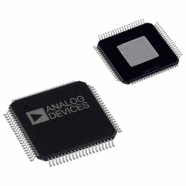
ICGOO电子元器件商城为您提供AD5757ACPZ由Analog设计生产,在icgoo商城现货销售,并且可以通过原厂、代理商等渠道进行代购。 AD5757ACPZ价格参考。AnalogAD5757ACPZ封装/规格:数据采集 - 数模转换器, 16 位 数模转换器 4 64-LFCSP-VQ(9x9)。您可以下载AD5757ACPZ参考资料、Datasheet数据手册功能说明书,资料中有AD5757ACPZ 详细功能的应用电路图电压和使用方法及教程。
AD5757ACPZ 是由 Analog Devices Inc. 生产的一款高性能数模转换器 (DAC),主要应用于高精度数据采集和控制领域。该器件具有以下应用场景:

1. 工业自动化与控制系统:AD5757ACPZ 可用于工业自动化系统中的精密控制,例如温度、压力、流量等传感器信号的采集与转换。它能够提供高分辨率和高精度的输出,确保控制系统能够精确地响应各种参数变化,适用于工厂自动化、过程控制等领域。

2. 测试与测量设备:在高精度测试仪器中,如示波器、信号发生器等,AD5757ACPZ 可以实现高精度的信号生成和测量。其低噪声和高线性度特性使得它非常适合用于需要高保真度信号处理的应用场合,确保测试结果的准确性。

3. 医疗设备:在医疗成像和监测设备中,如超声波设备、心电图机等,AD5757ACPZ 能够提供稳定且高精度的模拟信号输出,帮助提高诊断的准确性和可靠性。其低功耗和小尺寸设计也使其适合便携式医疗设备。

4. 通信系统:在无线通信基站和其他通信设备中,AD5757ACPZ 可用于信号调制和解调,提供稳定的射频信号输出。其高速转换能力和良好的动态性能有助于提升通信系统的传输质量。

5. 音频处理:在专业音频设备中,如数字音频工作站、音响设备等,AD5757ACPZ 可以用于将数字音频信号转换为高质量的模拟音频信号,提供清晰、无失真的声音输出。

总之,AD5757ACPZ 凭借其高精度、低噪声、宽工作温度范围等优点,广泛应用于对信号精度和稳定性要求极高的各个领域,确保系统能够可靠地进行数据采集和控制。
| 参数 | 数值 |
| 产品目录 | 集成电路 (IC)半导体 |
| 描述 | IC DAC 16BIT QUAD 64-LFCSP数模转换器- DAC Quad CH 16B IOUT |
| DevelopmentKit | EVAL-AD5757SDZ |
| 产品分类 | |
| 品牌 | Analog Devices |
| 产品手册 | |
| 产品图片 |
|
| rohs | 符合RoHS无铅 / 符合限制有害物质指令(RoHS)规范要求 |
| 产品系列 | 数据转换器IC,数模转换器- DAC,Analog Devices AD5757ACPZ- |
| 数据手册 | |
| 产品型号 | AD5757ACPZ |
| PCN设计/规格 | |
| 产品培训模块 | http://www.digikey.cn/PTM/IndividualPTM.page?site=cn&lang=zhs&ptm=26125http://www.digikey.cn/PTM/IndividualPTM.page?site=cn&lang=zhs&ptm=26140http://www.digikey.cn/PTM/IndividualPTM.page?site=cn&lang=zhs&ptm=26150http://www.digikey.cn/PTM/IndividualPTM.page?site=cn&lang=zhs&ptm=26147 |
| 产品种类 | 数模转换器- DAC |
| 位数 | 16 |
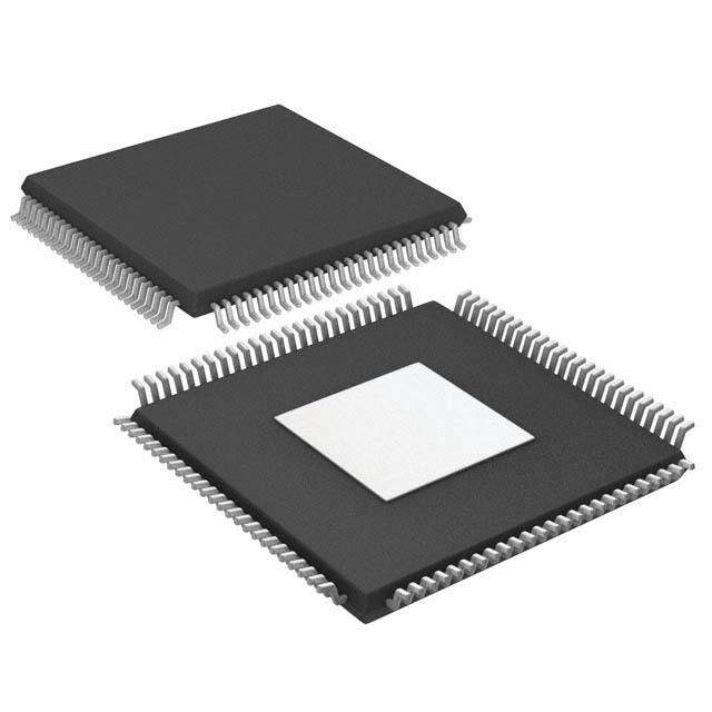
| 供应商器件封装 | 64-LFCSP-VQ(9x9) |
| 分辨率 | 16 bit |
| 包装 | 管件 |
| 商标 | Analog Devices |
| 安装类型 | 表面贴装 |
| 安装风格 | SMD/SMT |
| 封装 | Tray |
| 封装/外壳 | 64-VFQFN 裸露焊盘,CSP |
| 封装/箱体 | LFCSP-64 |
| 工作温度 | -40°C ~ 105°C |
| 工厂包装数量 | 260 |
| 建立时间 | 15µs |
| 接口类型 | SPI |
| 数据接口 | DSP,MICROWIRE™,QSPI™,串行,SPI™ |
| 最大功率耗散 | 155 mW |
| 最大工作温度 | + 105 C |
| 最小工作温度 | - 40 C |
| 标准包装 | 1 |
| 特色产品 | http://www.digikey.com/cn/zh/ph/Analog-Devices/ad5755-ad5755-1-ad5757.html |
| 电压参考 | Internal, External |
| 电压源 | 模拟和数字 |
| 电源电压-最大 | 5.5 V |
| 电源电压-最小 | 2.7 V |
| 积分非线性 | +/- 0.006 % FSR |
| 稳定时间 | 15 us |
| 系列 | AD5757 |
| 结构 | Segment |
| 转换器数 | 4 |
| 转换器数量 | 4 |
| 输出数和类型 | * |
| 输出类型 | Current |
| 采样比 | 60 kSPs |
| 采样率(每秒) | * |


- 商务部:美国ITC正式对集成电路等产品启动337调查
- 曝三星4nm工艺存在良率问题 高通将骁龙8 Gen1或转产台积电
- 太阳诱电将投资9.5亿元在常州建新厂生产MLCC 预计2023年完工
- 英特尔发布欧洲新工厂建设计划 深化IDM 2.0 战略
- 台积电先进制程称霸业界 有大客户加持明年业绩稳了
- 达到5530亿美元!SIA预计今年全球半导体销售额将创下新高
- 英特尔拟将自动驾驶子公司Mobileye上市 估值或超500亿美元
- 三星加码芯片和SET,合并消费电子和移动部门,撤换高东真等 CEO
- 三星电子宣布重大人事变动 还合并消费电子和移动部门
- 海关总署:前11个月进口集成电路产品价值2.52万亿元 增长14.8%


PDF Datasheet 数据手册内容提取
Quad Channel, 16-Bit, Serial Input, 4 mA to 20 mA Output DAC, Dynamic Power Control, HART Connectivity Data Sheet AD5757 FEATURES a dc-to-dc boost converter optimized for minimum on-chip power dissipation. 16-bit resolution and monotonicity Dynamic power control for thermal management Each channel has a corresponding CHART pin so that HART or external PMOS mode signals can be coupled onto the current output of the AD5757. Current output ranges: 0 mA to 20 mA, 4 mA to 20 mA, The part uses a versatile 3-wire serial interface that operates at or 0 mA to 24 mA clock rates of up to 30 MHz and is compatible with standard ±0.05% total unadjusted error (TUE) maximum SPI, QSPI™, MICROWIRE™, DSP, and microcontroller interface User programmable offset and gain standards. The interface also features optional CRC-8 packet On-chip diagnostics error checking, as well as a watchdog timer that monitors On-chip reference (±10 ppm/°C maximum) activity on the interface. −40°C to +105°C temperature range PRODUCT HIGHLIGHTS APPLICATIONS 1. Dynamic power control for thermal management. Process control 2. 16-bit performance. Actuator control 3. Multichannel. Programmable logic controllers (PLCs) 4. HART compliant. HART network connectivity COMPANION PRODUCTS GENERAL DESCRIPTION Product Family: AD5755-1, AD5755 The AD5757 is a quad, current output DAC that operates with a HART Modem: AD5700, AD5700-1 power supply range from 10.8 V to 33 V. On-chip dynamic External References: ADR445, ADR02 power control minimizes package power dissipation by regulat- Digital Isolators: ADuM1410, ADuM1411 ing the voltage on the output driver from 7.4 V to 29.5 V, using Power: ADP2302, ADP2303 Additional companion products on the AD5757 product page FUNCTIONAL BLOCK DIAGRAM AVCC 5.0V AVDD AGND +15V SWx VBOOST_x DVDD 7.4V TO 29.5V DGND LDAC DC-TO-DC CONVERTER SCLK SDIN SYNC INDTIEGRITFAALCE IOUT_x SDO + DAC A RSET_x CLEAR CURRENT AND VOLTAGE CHARTx FAULT OUTPUT RANGE ALERT GAIN REG A SCALING AD1 OFFSET REG A AD0 DAC CHANNEL A REFOUT REFERENCE REFIN DAC CHANNEL B DAC CHANNEL C AD5757 DAC CHANNEL D N1.O xT =E SA, B, C, AND D. 09225-101 Figure 1. Rev. G Document Feedback Information furnished by Analog Devices is believed to be accurate and reliable. However, no responsibility is assumed by Analog Devices for its use, nor for any infringements of patents or other One Technology Way, P.O. Box 9106, Norwood, MA 02062-9106, U.S.A. rights of third parties that may result from its use. Specifications subject to change without notice. No license is granted by implication or otherwise under any patent or patent rights of Analog Devices. Tel: 781.329.4700 ©2011–2017 Analog Devices, Inc. All rights reserved. Trademarks and registered trademarks are the property of their respective owners. Technical Support www.analog.com
AD5757 Data Sheet TABLE OF CONTENTS Features........................................................................................... 1 Readback Operation ................................................................ 32 Applications ................................................................................... 1 Device Features ............................................................................ 34 General Description ...................................................................... 1 Output Fault ............................................................................. 34 Product Highlights ........................................................................ 1 Digital Offset and Gain Control ............................................. 34 Companion Products .................................................................... 1 Status Readback During a Write............................................. 34 Functional Block Diagram ............................................................ 1 Asynchronous Clear ................................................................ 34 Revision History ............................................................................ 3 Packet Error Checking ............................................................ 35 Detailed Functional Block Diagram............................................. 4 Watchdog Timer ...................................................................... 35 Specifications ................................................................................. 5 Output Alert............................................................................. 35 AC Performance Characteristics .............................................. 7 Internal Reference.................................................................... 35 Timing Characteristics .............................................................. 7 External Current Setting Resistor........................................... 35 Absolute Maximum Ratings ....................................................... 10 HART........................................................................................ 36 ESD Caution............................................................................. 10 Digital Slew Rate Control........................................................ 36 Pin Configuration and Function Descriptions.......................... 11 Power Dissipation Control...................................................... 37 Typical Performance Characteristics.......................................... 14 DC-to-DC Converters............................................................. 37 Current Outputs ...................................................................... 14 AI Supply Requirements—Static ......................................... 38 CC DC-to-DC Block...................................................................... 19 AI Supply Requirements—Slewing ..................................... 38 CC Reference .................................................................................. 20 External PMOS Mode ............................................................. 40 General ..................................................................................... 21 Applications Information............................................................ 41 Terminology ................................................................................. 22 Current Output Mode with Internal R ............................... 41 SET Theory of Operation.................................................................... 23 Precision Voltage Reference Selection.................................... 41 DAC Architecture .................................................................... 23 Driving Inductive Loads ......................................................... 41 Power-On State of the AD5757 .............................................. 23 Transient Voltage Protection................................................... 42 Serial Interface ......................................................................... 23 Microprocessor Interfacing..................................................... 42 Transfer Function .................................................................... 24 Layout Guidelines .................................................................... 42 Registers ....................................................................................... 25 Galvanically Isolated Interface................................................ 43 Programming Sequence to Write/Enable the Output Industrial HART Capable Analog Output Application ........ 44 Correctly................................................................................... 26 Outline Dimensions .................................................................... 45 Changing and Reprogramming the Range ............................ 26 Ordering Guide........................................................................ 45 Data Registers .......................................................................... 27 Control Registers ..................................................................... 29 Rev. G | Page 2 of 45
Data Sheet AD5757 REVISION HISTORY 6/2017—Rev. F to Rev. G 5/2012—Rev. B to Rev. C Changes to Figure 4 ........................................................................8 Changes to Companion Products Section ....................................1 Changes to Figure 5 ........................................................................9 Changes to Table 5 ........................................................................13 Changes to Readback Operation Section....................................32 Added Industrial HART Capable Analog Output Application Deleted Table 27 and Table 28; Renumbered Sequentially ........32 Section and Figure 66, Renumbered Sequentially......................43 Changes to Asynchronous Clear Section ....................................34 Updated Outline Dimensions ......................................................44 9/2014—Rev. E to Rev. F 11/2011—Rev. A to Rev. B Changes to Table 3 ..........................................................................7 Change to Test Conditions/Comments of Accuracy (External Changes to Pin 21 and Pin 29 Descriptions................................12 R ) Parameter, Table 1..................................................................5 SET Changes to Pin 51 and Pin 59 Descriptions................................13 Changes to Figure 4 ........................................................................8 Changes to Figure 45......................................................................21 Changes to Figure 5 ........................................................................9 Changes to Software Register and Status Register Descriptions .25 Change to Pin 8 Description, Table 5..........................................11 Changes to Software Register Section, Table 21, and Table 22 ...31 Change to Figure 13......................................................................14 Changed Bit 11 of the Status Register; Table 30 and Table 31 ...34 Change to Figure 20......................................................................16 Changes to Packet Error Checking Section ................................36 Changes to Figure 48 and Power-On State of the AD5757 Changes to HART Section ...........................................................37 Section ...........................................................................................23 Change to Table 16 .......................................................................29 6/2014—Rev. D to Rev. E Changes to Readback Operation Section, Readback Example Change to Thermal Hysteresis Parameter and Power Section, and Table 25 ....................................................................32 Dissipation Parameter, Table 1 ......................................................6 Change to Figure 54......................................................................35 Changes to Table 3 ..........................................................................7 Change to Figure 58 Caption .......................................................38 Changes to Figure 4 ........................................................................8 Changes to Figure 59, Figure 60, and Figure 61 Captions .........39 Added Figure 5; Renumbered Sequentially, Changes to Figure 6 ....9 Changes to Transient Voltage Protection Section and Change to Figure 30......................................................................17 Figure 63........................................................................................41 Changes to Figure 34, Figure 35, Figure 36, and Figure 37 .......19 Changes to Galvanically Isolated Interface Section ...................42 Changes to Figure 45 and Figure 47 ............................................21 Change to Voltage Reference Thermal Hysteresis Definition ...22 5/2011—Rev. 0 to Rev. A Changes to Table 6 ........................................................................25 Changes Features Section...............................................................1 Changes to Table 11 and Table 13................................................28 Changes to Figure 2 ........................................................................3 Changes to Software Register Section, Table 21, and Table 22 .......31 Changed AV Min Parameter from 10.8 V to 9 V......................5 DD Changes to Readback Operation Section, Added Table 27 and Changes to Pin 22, Pin31, Pin 49 Descriptions ..........................11 Table 28; Renumbered Sequentially ............................................32 Changes to Pin 58 Descriptions...................................................12 Changes to Status Register Section, Table 30, and Table 31 ......34 Changes to Figure 8, Figure 9, and Figure 10 .............................13 Changes to Status Readback During a Write Section ................35 Added Figure 23, Renumbered Sequentially ..............................15 Changes to Packet Error Checking Section ................................36 Added Figure 29............................................................................16 Changes to Table 35 ......................................................................38 Added External PMOS Mode Section and Figure 62 ................38 Change to External PMOS Mode Section and Figure 63 ..........40 4/2011—Revision 0: Initial Version 11/2012—Rev. C to Rev. D Changed Thermal Impedance from 20°C/W to 28°C/W ..........10 Changes to Pin 6 Description ......................................................11 Changes to DUT_AD1, DUT_AD0 Description, Table 8 .........27 Changes to Changes to Packet Error Checking Section and Internal Reference Section ...........................................................35 Changes to Figure 57 ....................................................................37 Changes to Figure 63 ....................................................................41 Changes to Figure 66 ....................................................................43 Updated Outline Dimensions ......................................................44 Rev. G | Page 3 of 45
AD5757 Data Sheet DETAILED FUNCTIONAL BLOCK DIAGRAM AVCC 5.0V AVDD AGND +15V SWA VBOOST_A DVDD POWER-ON DC-TO-DC DGND RESET CONVERTER LDAC POWER 7.4V TO 29.5V VSEN1 VSEN2 CONTROL REG CLEAR INPUT SHIFT SSCDLIKN REGAINSDTER 16 INPUT + DAC 16 DAC A R2 R3 SYNC CONTROL REG A REG A SDO FAULT GAIN REG A IOUT_A OFFSET REG A STATUS REGISTER ALERT WATCHDOG R1 RSET_A TIMER (SPI ACTIVITY) CHARTA REFOUT VREF DAC CHANNEL A REFERENCE REFIN BUFFERS IOUT_B, IOUT_C, IOUT_D DAC CHANNEL B RSET_B, RSET_C, RSET_D AD1 AD5757 DAC CHANNEL C CHARTB, CHARTC, CHARTD AD0 DAC CHANNEL D SWB, SWC, SWD VBOOST_B,VBOOST_C,VBOOST_D 09225-001 Figure 2. Rev. G | Page 4 of 45
Data Sheet AD5757 SPECIFICATIONS AV = V = 15 V; DV = 2.7 V to 5.5 V; AV = 4.5 V to 5.5 V; dc-to-dc converter disabled; AGND = DGND = GNDSW = 0 V; DD BOOST_x DD CC x REFIN = 5 V; R = 300 Ω; all specifications T to T , unless otherwise noted. L MIN MAX Table 1. Parameter1 Min Typ Max Unit Test Conditions/Comments CURRENT OUTPUT Output Current Ranges 0 24 mA 0 20 mA 4 20 mA Resolution 16 Bits ACCURACY (EXTERNAL RSET) Assumes ideal resistor; see the External Current Setting Resistor section for more information Total Unadjusted Error (TUE) −0.05 ±0.009 +0.05 % FSR TUE Long-Term Stability 100 ppm FSR Drift after 1000 hours, TJ = 150°C Relative Accuracy (INL) −0.006 +0.006 % FSR Differential Nonlinearity (DNL) −1 +1 LSB Guaranteed monotonic Offset Error −0.05 ±0.005 +0.05 % FSR Offset Error Drift2 ±4 ppm FSR/°C Gain Error −0.05 ±0.004 +0.05 % FSR Gain TC2 ±3 ppm FSR/°C Full-Scale Error −0.05 ±0.008 +0.05 % FSR Full-Scale TC2 ±5 ppm FSR/°C DC Crosstalk 0.0005 % FSR External RSET ACCURACY (INTERNAL RSET) Total Unadjusted Error (TUE)3, 4 −0.14 +0.14 % FSR −0.11 ±0.009 +0.11 % FSR TA = 25°C TUE Long-Term Stability 180 ppm FSR Drift after 1000 hours, TJ = 150°C Relative Accuracy (INL) −0.006 +0.006 % FSR −0.004 +0.004 % FSR TA = 25°C Differential Nonlinearity (DNL) −1 +1 LSB Guaranteed monotonic Offset Error3, 4 −0.05 +0.05 % FSR −0.04 ±0.007 +0.04 % FSR TA = 25°C Offset Error Drift2 ±6 ppm FSR/°C Gain Error −0.12 +0.12 % FSR −0.06 ±0.002 +0.06 % FSR TA = 25°C Gain TC2 ±9 ppm FSR/°C Full-Scale Error3, 4 −0.14 +0.14 % FSR −0.1 ±0.007 +0.1 % FSR TA = 25°C Full-Scale TC2 ±14 ppm FSR/°C DC Crosstalk4 −0.011 % FSR Internal RSET OUTPUT CHARACTERISTICS2 Current Loop Compliance Voltage VBOOST_x − VBOOST_x − V 2.4 2.7 Output Current Drift vs. Time Drift after 1000 hours, ¾ scale output, TJ = 150°C 90 ppm FSR External RSET 140 ppm FSR Internal RSET Resistive Load 1000 Ω The dc-to-dc converter has been characterized with a maximum load of 1 kΩ, chosen such that compliance is not exceeded; see Figure 32 and DC-DC MaxV bits in Table 24 Output Impedance 100 MΩ DC PSRR 0.02 1 µA/V REFERENCE INPUT/OUTPUT Reference Input2 Reference Input Voltage 4.95 5 5.05 V For specified performance DC Input Impedance 45 150 MΩ Rev. G | Page 5 of 45
AD5757 Data Sheet Parameter1 Min Typ Max Unit Test Conditions/Comments Reference Output Output Voltage 4.995 5 5.005 V TA = 25°C Reference TC2 −10 ±5 +10 ppm/°C Output Noise (0.1 Hz to 10 Hz)2 7 µV p-p Noise Spectral Density2 100 nV/√Hz At 10 kHz Output Voltage Drift vs. Time2 180 ppm Drift after 1000 hours, TJ = 150°C Capacitive Load2 1000 nF Load Current 9 mA See Figure 43 Short-Circuit Current 10 mA Line Regulation2 3 ppm/V See Figure 44 Load Regulation2 95 ppm/mA See Figure 43 Thermal Hysteresis2 200 ppm DC-TO-DC Switch Switch On Resistance 0.425 Ω Switch Leakage Current 10 nA Peak Current Limit 0.8 A Oscillator Oscillator Frequency 11.5 13 14.5 MHz This oscillator is divided down to give the dc-to-dc converter switching frequency Maximum Duty Cycle 89.6 % At 410 kHz dc-to-dc switching frequency DIGITAL INPUTS2 JEDEC compliant VIH, Input High Voltage 2 V VIL, Input Low Voltage 0.8 V Input Current −1 +1 µA Per pin Pin Capacitance 2.6 pF Per pin DIGITAL OUTPUTS2 SDO, ALERT VOL, Output Low Voltage 0.4 V Sinking 200 µA VOH, Output High Voltage DVDD − 0.5 V Sourcing 200 µA High Impedance Leakage Current −1 +1 µA High Impedance Output 2.5 pF Capacitance FAULT VOL, Output Low Voltage 0.4 V 10 kΩ pull-up resistor to DVDD VOL, Output Low Voltage 0.6 V At 2.5 mA VOH, Output High Voltage 3.6 V 10 kΩ pull-up resistor to DVDD POWER REQUIREMENTS AVDD 9 33 V DVDD 2.7 5.5 V AVCC 4.5 5.5 V AIDD 7 7.5 mA DICC 9.2 11 mA VIH = DVDD, VIL = DGND, internal oscillator running, over supplies AICC 1 mA Over supplies IBOOST5 1 mA Per channel, current output mode, 0 mA output Power Dissipation 155 mW AVDD = 15 V, DVDD = 5 V, dc-to-dc converter enable, current output mode, outputs disabled 1 Temperature range: −40°C to +105°C; typical at +25°C. 2 Guaranteed by design and characterization; not production tested. 3 For current outputs with internal RSET, the offset, full-scale, and TUE measurements exclude dc crosstalk. The measurements are made with all four channels enabled loaded with the same code. 4 See the Current Output Mode with Internal RSET section for more explanation of the dc crosstalk. 5 Efficiency plots in Figure 34, Figure 35, Figure 36, and Figure 37 include the IBOOST quiescent current. Rev. G | Page 6 of 45
Data Sheet AD5757 AC PERFORMANCE CHARACTERISTICS AV = V = 15 V; DV = 2.7 V to 5.5 V; AV = 4.5 V to 5.5 V; dc-to-dc converter disabled; AGND = DGND = GNDSW = 0 V; DD BOOST_x DD CC x REFIN = 5 V; R = 300 Ω; all specifications T to T , unless otherwise noted. L MIN MAX Table 2. Parameter1 Min Typ Max Unit Test Conditions/Comments DYNAMIC PERFORMANCE Current Output Output Current Settling Time 15 µs To 0.1% FSR (0 mA to 24 mA) See test conditions/ ms See Figure 27, Figure 28, and Figure 29 comments Output Noise (0.1 Hz to 10 Hz 0.15 LSB p-p 16-bit LSB, 0 mA to 24 mA range Bandwidth) Output Noise Spectral Density 0.5 nA/√Hz Measured at 10 kHz, midscale output, 0 mA to 24 mA range 1 Guaranteed by design and characterization; not production tested. TIMING CHARACTERISTICS AV = V = 15 V; DV = 2.7 V to 5.5 V; AV = 4.5 V to 5.5 V; dc-to-dc converter disabled; AGND = DGND = GNDSW = 0 V; DD BOOST_x DD CC x REFIN = 5 V; R = 300 Ω; all specifications T to T , unless otherwise noted. L MIN MAX Table 3. Parameter1, 2, 3 Limit at T , T Unit Description MIN MAX t 33 ns min SCLK cycle time 1 t 13 ns min SCLK high time 2 t 13 ns min SCLK low time 3 t4 13 ns min SYNC falling edge to SCLK falling edge setup time t5 13 ns min 24th/32nd SCLK falling edge to SYNC rising edge (see Figure 55) t6 198 ns min SYNC high time after a configuration write 5 µs min SYNC high time after a DAC update write t 5 ns min Data setup time 7 t 5 ns min Data hold time 8 t9 20 µs min SYNC rising edge to LDAC falling edge (applies to any channel that has digital slew rate control enabled) (single DAC updated) 5 µs min SYNC rising edge to LDAC falling edge (single DAC updated) t10 10 ns min LDAC pulse width low t11 500 ns max LDAC falling edge to DAC output response time t See the AC Performance µs max DAC output settling time 12 Characteristics section t 10 ns min CLEAR high time 13 t 5 µs max CLEAR activation time 14 t 40 ns max SCLK rising edge to SDO valid 15 t16 5 µs min SYNC rising edge to DAC output response time (LDAC = 0) (single DAC updated) t17 500 ns min LDAC falling edge to SYNC rising edge t18 800 ns min RESET pulse width t19 20 µs min SYNC high to next SYNC low (digital slew rate control enabled) (single DAC updated) 5 µs min SYNC high to next SYNC low (digital slew rate control disabled) (single DAC updated) 1 Guaranteed by design and characterization; not production tested. 2 All input signals are specified with tRISE = tFALL = 5 ns (10% to 90% of DVDD) and timed from a voltage level of 1.2 V. 3 See Figure 3, Figure 4, Figure 6, and Figure 7. Rev. G | Page 7 of 45
AD5757 Data Sheet Timing Diagrams t1 SCLK 1 2 24 t6 t3 t2 t4 t5 SYNC t7 t8 t19 SDIN MSB LSB t10 t10 t9 LDAC t17 t12 t11 IOUT_x LDAC = 0 t12 t16 IOUT_x t13 CLEAR t14 IOUT_x RESET t18 09225-002 Figure 3. Serial Interface Timing Diagram SCLK 1 24 1 24 t6 SYNC SDIN MSB LSB MSB LSB INPUT WORD SPECIFIES NOP CONDITION REGISTERTO BE READ SDO MSB LSB UNDEFINED SELECTED REGISTER DATA SEE THE READBACK OPERATION SECTION FOR FURTHER INFORMATION. t15 CLOCKED OUT 09225-003 Figure 4. Readback Timing Diagram (Packet Error Checking Disabled) Rev. G | Page 8 of 45
Data Sheet AD5757 SCLK 1 24 32 1 24 32 t61 SYNC SDIN MSB LSB CRC7 CRC0 MSB LSB CRC7 CRC0 INPUT WORD SPECIFIES 8-BIT CRC NOP 8-BIT CRC REGISTERTO BE READ CONDITION SDO MSB LSB UNDEFINED 8-BIT CRC t15 SELECTED REGISTER DATA CLOCKED OUT 1SAEVEOITDH SECRLEKAADCBTAIVCIKTY O DPUERRIANGTIOt6NAASN ITDMPAACYKREETSEURLTR OINRACHPEECCKEIRNRGOSRE OCTNIORNESADFBOARCFKU.RTHER INFORMATION. 09225-105 Figure 5. Readback Timing Diagram (Packet Error Checking Enabled) LSB MSB 1 2 24 SCLK SYNC SDIN R/W DUT_ DUT_ X X X D15 D14 D1 D0 AD1 AD0 SDO SDO DISABLED ESNDAOB_ STATUS STATUS STATUS STATUS 09225-004 Figure 6. Status Readback During Write 200µA IOL TO OUTPUT VOH (MIN) OR PIN CL VOL (MAX) 50pF 200µA IOH 09225-005 Figure 7. Load Circuit for SDO Timing Diagram Rev. G | Page 9 of 45
AD5757 Data Sheet ABSOLUTE MAXIMUM RATINGS T = 25°C, unless otherwise noted. Transient currents of up to A Stresses at or above those listed under Absolute Maximum 100 mA do not cause SCR latch-up. Ratings may cause permanent damage to the product. This is a stress rating only; functional operation of the product at these Table 4. or any other conditions above those indicated in the operational Parameter Rating section of this specification is not implied. Operation beyond AV , V to AGND, DGND −0.3 V to +33 V DD BOOST_x the maximum operating conditions for extended periods may AV to AGND −0.3 V to +7 V CC affect product reliability. DV to DGND −0.3 V to +7 V DD Digital Inputs to DGND −0.3 V to DVDD + 0.3 V or +7 V ESD CAUTION (whichever is less) Digital Outputs to DGND −0.3 V to DVDD + 0.3 V or +7 V (whichever is less) REFIN, REFOUT to AGND −0.3 V to AVDD + 0.3 V or +7 V (whichever is less) IOUT_x to AGND AGND to VBOOST_x or 33 V if using the dc-to-dc circuitry SW to AGND −0.3 V to +33 V x AGND, GNDSW to DGND −0.3 V to +0.3 V x Operating Temperature Range (T ) A Industrial1 −40°C to +105°C Storage Temperature Range −65°C to +150°C Junction Temperature (T max) 125°C J 64-Lead LFCSP θ Thermal Impedance2 28°C/W JA Power Dissipation (T max – T )/θ J A JA Lead Temperature JEDEC industry standard Soldering J-STD-020 1 Power dissipated on chip must be derated to keep the junction temperature below 125°C. 2 Based on a JEDEC 4-layer test board. Rev. G | Page 10 of 45
Data Sheet AD5757 PIN CONFIGURATION AND FUNCTION DESCRIPTIONS D C_ DD RSET_CRSET_DREFOUTREFINNCCHARTDIGATEDCOMPDCVBOOST_NCIOUT_DAGNDNCCHARTCNCIGATEC 4321098765432109 6666655555555554 PIN 1 INDICATOR RSET_B 1 48COMPDCDC_C RSET_A 2 47IOUT_C REFGND 3 46VBOOST_C REFGND 4 45AVCC AD0 5 44SWC AD1 6 43GNDSWC SYNC 7 AD5757 42GNDSWD SCLK 8 TOP VIEW 41SWD SDIN 9 40AGND (Not to Scale) SDO10 39SWA DVDD11 38GNDSWA DGND12 37GNDSWB LDAC13 36SWB CLEAR14 35AGND ALERT15 34VBOOST_B FAULT16 33IOUT_B 7890123456789012 1112222222222333 DT DCAA AAC ADCBCB B DGNRESEAVDNHARTGATE DCDC_OOST_NIOUT_AGNNHARTNGATE DCDC_ CIP B C IP MV M O O C C NOTES 1. NC = NO CONNECT. DO NOT CONNECT TO THIS PIN. 2.THE EXPOSED PAD SHOULD BE CONNECTED TO AGND, OR ALTERNATIVELY, ITTTHH CEEA RPNMA ABDLE B PLEEE TRFHFTEO ERRLMMEACALTNLRCYIEC C.AOLNLNYE UCNTCEODN TNOE CAT CEODP. PITE IRS PRLEACNOEM FMOERN EDNEHDA TNHCAETD 09225-006 Figure 8. Pin Configuration Table 5. Pin Function Descriptions Pin No. Mnemonic Description 1 RSET_B An external, precision, low drift 15 kΩ current setting resistor can be connected to this pin to improve the IOUT_B temperature drift performance. See the Device Features section. 2 RSET_A An external, precision, low drift 15 kΩ current setting resistor can be connected to this pin to improve the IOUT_A temperature drift performance. See the Device Features section. 3, 4 REFGND Ground Reference Point for Internal Reference. 5 AD0 Address Decode for the Device Under Test (DUT) on the Board. 6 AD1 Address Decode for the DUT on the Board. It is not recommended to tie both AD1 and AD0 low when using PEC, see the Packet Error Checking section. 7 SYNC Active Low Input. This is the frame synchronization signal for the serial interface. While SYNC is low, data is transferred in on the falling edge of SCLK. 8 SCLK Serial Clock Input. Data is clocked into the input shift register on the falling edge of SCLK. This pin operates at clock speeds of up to 30 MHz. 9 SDIN Serial Data Input. Data must be valid on the falling edge of SCLK. 10 SDO Serial Data Output. Used to clock data from the serial register in readback mode. See Figure 4 and Figure 6. 11 DV Digital Supply. The voltage range is from 2.7 V to 5.5 V. DD 12, 17 DGND Digital Ground. 13 LDAC Load DAC, Active Low Input. This is used to update the DAC register and consequently the DAC outputs. When tied permanently low, the addressed DAC data register is updated on the rising edge of SYNC. If LDAC is held high during the write cycle, the DAC input register is updated, but the DAC output update only takes place at the falling edge of LDAC (see Figure 3). Using this mode, all analog outputs can be updated simultaneously. The LDAC pin must not be left unconnected. 14 CLEAR Active High, Edge Sensitive Input. Asserting this pin sets the output current and voltage to the preprogrammed clear code bit setting. Only channels enabled to be cleared are cleared. See the Device Features section for more information. When CLEAR is active, the DAC output register cannot be written to. Rev. G | Page 11 of 45
AD5757 Data Sheet Pin No. Mnemonic Description 15 ALERT Active High Output. This pin is asserted when there has been no SPI activity on the interface pins for a predetermined time. See the Device Features section for more information. 16 FAULT Active Low Output. This pin is asserted low when an open circuit in current mode is detected, a short circuit in voltage mode is detected, a PEC error is detected, or an overtemperature is detected (see the Device Features section). Open-drain output. 18 RESET Hardware Reset. Active Low Input. 19 AV Positive Analog Supply. The voltage range is from 10.8 V to 33 V. DD 20, 25, NC No Connect. Do not connect to this pin. 28, 30, 50, 52, 55, 60 21 CHARTA HART Input Connection for DAC Channel A. For more information, see the HART section. If unused, leave as an open circuit. 22 IGATEA Optional Connection for External Pass Transistor. Leave unconnected when using the dc-to-dc converter. See the External PMOS Mode section for more information. 23 COMP DC-to-DC Compensation Capacitor. Connect a 10 nF capacitor from this pin to ground. Used to regulate the DCDC_A feedback loop of the Channel A dc-to-dc converter. Alternatively, if using an external compensation resistor, place a resistor in series with a capacitor to ground from this pin (see the DC-to-DC Converter Compensation Capacitors and the AICC Supply Requirements—Slewing sections in the Device Features section for more information). 24 V Supply for Channel A Current Output Stage (see Figure 50). To use the dc-to-dc feature of the device, connect as BOOST_A shown in Figure 57. 26 I Current Output Pin for DAC Channel A. OUT_A 27, 40, 53 AGND Ground Reference Point for Analog Circuitry. This must be connected to 0 V. 29 CHARTB HART Input Connection for DAC Channel B. For more information, see the HART section. If unused, leave as an open circuit. 31 IGATEB Optional Connection for External Pass Transistor. Leave unconnected when using the dc-to-dc converter. See the External PMOS Mode section for more information. 32 COMP DC-to-DC Compensation Capacitor. Connect a 10 nF capacitor from this pin to ground. Used to regulate the DCDC_B feedback loop of the Channel B dc-to-dc converter. Alternatively, if using an external compensation resistor, place a resistor in series with a capacitor to ground from this pin (see the DC-to-DC Converter Compensation Capacitors and AI Supply Requirements—Slewing sections in the Device Features section for more CC information). 33 I Current Output Pin for DAC Channel B. OUT_B 34 V Supply for Channel B Current Output Stage (see Figure 50). To use the dc-to-dc feature of the device, connect as BOOST_B shown in Figure 57. 35 AGND Ground Reference Point for Analog Circuitry. This pin must be connected to 0 V. 36 SW Switching Output for Channel B DC-to-DC Circuitry. To use the dc-to-dc feature of the device, connect as shown B in Figure 57. 37 GNDSW Ground Connection for DC-to-DC Switching Circuit. This pin must always be connected to ground. B 38 GNDSW Ground Connection for DC-to-DC Switching Circuit. This pin must always be connected to ground. A 39 SW Switching Output for Channel A DC-to-DC Circuitry. To use the dc-to-dc feature of the device, connect as shown A in Figure 57. 41 SW Switching Output for Channel D DC-to-DC Circuitry. To use the dc-to-dc feature of the device, connect as shown D in Figure 57. 42 GNDSW Ground Connections for DC-to-DC Switching Circuit. This pin must always be connected to ground. D 43 GNDSW Ground Connections for DC-to-DC Switching Circuit. This pin must always be connected to ground. C 44 SW Switching Output for Channel C DC-to-DC Circuitry. To use the dc-to-dc feature of the device, connect as shown C in Figure 57. 45 AV Supply for DC-to-DC Circuitry. CC 46 V Supply for Channel C Current Output Stage (see Figure 50). To use the dc-to-dc feature of the device, connect as BOOST_C shown in Figure 57. 47 I Current Output Pin for DAC Channel C. OUT_C 48 COMP DC-to-DC Compensation Capacitor. Connect a 10 nF capacitor from this pin to ground. Used to regulate the DCDC_C feedback loop of the Channel C dc-to-dc converter. Alternatively, if using an external compensation resistor, place a resistor in series with a capacitor to ground from this pin (see the DC-to-DC Converter Compensation Capacitors and AICC Supply Requirements—Slewing sections in the Device Features section for more information). Rev. G | Page 12 of 45
Data Sheet AD5757 Pin No. Mnemonic Description 49 IGATEC Optional Connection for External Pass Transistor. Leave unconnected when using the dc-to-dc converter. See the External PMOS Mode section for more information. 51 CHARTC HART Input Connection for DAC Channel C. For more information, see the HART section. If unused, leave as an open circuit. 54 I Current Output Pin for DAC Channel D. OUT_D 56 V Supply for Channel D Current Output Stage (see Figure 50). To use the dc-to-dc feature of the device, connect as BOOST_D shown in Figure 57. 57 COMP DC-to-DC Compensation Capacitor. Connect a 10 nF capacitor from this pin to ground. Used to regulate the DCDC_D feedback loop of the Channel D dc-to-dc converter. Alternatively, if using an external compensation resistor, place a resistor in series with a capacitor to ground from this pin (see the DC-to-DC Converter Compensation Capacitors and AI Supply Requirements—Slewing sections in t section for more information). CC 58 IGATED Optional Connection for External Pass Transistor. Leave unconnected when using the dc-to-dc converter. See the External PMOS Mode section for more information. 59 CHARTD HART Input Connection for DAC Channel D. For more information, see the HART section. If unused, leave as an open circuit. 61 REFIN External Reference Voltage Input. 62 REFOUT Internal Reference Voltage Output. It is recommended to place a 0.1 µF capacitor between REFOUT and REFGND. REFOUT must be connected to REFIN to use the internal reference. 63 RSET_D An external, precision, low drift 15 kΩ current setting resistor can be connected to this pin to improve the IOUT_D temperature drift performance. See the Device Features section. 64 RSET_C An external, precision, low drift 15 kΩ current setting resistor can be connected to this pin to improve the IOUT_C temperature drift performance. See the Device Features section. EPAD Exposed Pad. This exposed pad must be connected to AGND, or, alternatively, it can be left electrically unconnected. It is recommended that the pad be thermally connected to a copper plane for enhanced thermal performance. Rev. G | Page 13 of 45
AD5757 Data Sheet TYPICAL PERFORMANCE CHARACTERISTICS CURRENT OUTPUTS 0.0025 0.0010 AVDD = 15V 0.0020 TA = 25°C 0.0008 0.0015 0.0006 %FSR) 00..00000150 %FSR) 00..00000024 40mmAA TTOO 2204mmAA RRAANNGGEE MMAAXX IINNLL AVDD = 15V OR ( 0 OR ( 0 00mmAA TTOO 2200mmAA RRAANNGGEE MMAINX I NINLL R R R R 4mA TO 20mA RANGE MAX INL L E–0.0005 L E–0.0002 0mA TO 24mA RANGE MIN INL N N I–0.0010 I–0.0004 –0.0015 4mATO 20mA, EXTERNAL RSET –0.0006 4mATO 20mA, EXTERNAL RSET, WITH DC-TO-DC CONVERTER –0.0020 4mATO 20mA, INTERNAL RSET –0.0008 4mATO 20mA, INTERNAL RSET, WITH DC-TO-DC CONVERTER 4mATO 20mA, EXTERNAL RSET, EXTERNAL PMOS MODE –0.00250 10000 20000 300C0O0DE 40000 50000 60000 09225-149 –0.0010–40 –20 0 TEM2P0ERATU4R0E (°C)60 80 100 09225-152 Figure 9. Integral Nonlinearity vs. Code Figure 12. Integral Nonlinearity vs. Temperature, Internal RSET 1.0 0.0020 0.8 44mmAATTOO 2200mmAA,, EEXXTTEERRNNAALL RRSSEETT, WITH DC-TO-DC CONVERTER 4mA TO 20mA RANGE MAX INL 4mATO 20mA, INTERNAL RSET 0.0015 0mA TO 24mA RANGE MAX INL 0.6 44mmAATTOO 2200mmAA,, IENXTTEERRNNAALL R RSSEETT, ,W EIXTTHE DRCN-ATLO -PDMCO CSO MNOVEDRETER 0mA TO 20mA RANGE MIN INL 0.0010 ROR (LSB) 00..240 OR (%FSR) 0.00050 04mmAA TTOO 2200mmAA RRAANNGGEE MMAINX I NINLL R R 0mA TO 24mA RANGE MIN INL E R NL –0.2 L E–0.0005 D N –0.4 I –0.0010 –0.6 –0.8 ATAV D=D 2 =5° 1C5V –0.0015 AVDD = 15V –1.00 10000 20000 300C0O0DE 40000 50000 60000 09225-150 –0.0020–40 –20 0 TEM2P0ERATU4R0E (°C)60 80 100 09225-153 Figure 10. Differential Nonlinearity vs. Code Figure 13. Integral Nonlinearity vs. Temperature, External RSET 0.035 1.0 R) 0.030 ATAAVL LD= D C2 =5H° A1C5NVNELS ENABLED 0.8 AIANLVTLDE DRR =AN NA15GLV EASND EXTERNAL RSET FS 0.025 0.6 % ROR ( 0.020 4mATO 20mA, EXTERNAL RSET SB) 0.4 JUSTED ER 000...000011505 4444mmmmAAAATTTTOOOO 22220000mmmmAAAA,,,, EIIENNXXTTTTEEEERRRRNNNNAAAALLLL RR RRSSSSEEEETTTT, ,,W WEIXTITTHHE D RDCNC-AT-TLOO -P-DMDCCO C SCO OMNNOVVEDERERTTEERR L ERROR (L–00..220 DDNNLL EERRRROORR MMAINX D N A D UN 0 –0.4 L TA–0.005 –0.6 O T –0.010 –0.8 –0.0150 10000 20000 300C0O0DE 40000 50000 60000 09225-151 –1.0–40 –20 0 TEM2P0ERATU4R0E (°C)60 80 100 09225-154 Figure 11. Total Unadjusted Error vs. Code Figure 14. Differential Nonlinearity vs. Temperature Rev. G | Page 14 of 45
Data Sheet AD5757 0.03 0.02 0.02 R) 0.01 S 0.01 F % 0 RROR (–0.010 %FSR)–0.01 D E–0.02 R ( TE RO–0.02 TOTAL UNADJSU–––––00000.....0000076543 440000mmmmmmAAAAAAAV TTTTTTDOOOOOOD =222222 0000441mmmmmm5VAAAAAA IEIEEINNNXXXTTTTTTEEEEEERRRRRRNNNNNNAAAAAALLLLLL RRR RRRSSSSSSEEEEEETTTTTT GAIN ER–––000...000534 AV440000DmmmmmmDAAAAAA = TTTTTT 1OOOOOO5 V222222000044mmmmmmAAAAAA IEIEEINNNXXXTTTTTTEEEEEERRRRRRNNNNNNAAAAAALLLLLL RRR RRRSSSSSSEEEEEETTTTTT –0.08–40 –20 0 TEM2P0ERATU4R0E (°C)60 80 100 09225-155 –0.06–40 –20 0 TEM2P0ERATU4R0E (°C)60 80 100 09225-159 Figure 15. Total Unadjusted Error vs. Temperature Figure 18. Gain Error vs. Temperature 0.03 0.0025 4mA TO 20mA RANGE MAX INL 0.02 0.0020 4mA TO 20mA RANGE MIN INL 0.01 TA= 25°C R) 0.0015 FS 0 OR (%–0.01 %FSR) 0.0010 RR–0.02 R ( 0.0005 E O LE –0.03 AVDD = 15V RR 0 A E L-SC–0.04 40mmAA TTOO 2200mmAA IINNTTEERRNNAALL RRSSEETT INL –0.0005 UL–0.05 0mA TO 24mA INTERNAL RSET F–0.06 4mA TO 20mA EXTERNAL RSET –0.0010 0mA TO 20mA EXTERNAL RSET –0.07 0mA TO 24mA EXTERNAL RSET –0.0015 –0.08–40 –20 0 TEM2P0ERATU4R0E (°C)60 80 100 09225-157 –0.002010 15 S2U0PPLY (V) 25 30 09225-056 Figure 16. Full-Scale Error vs. Temperature Figure 19. Integral Nonlinearity Error vs. AVDD, Over Supply, External RSET 0.020 0.0015 0.015 0.0010 R) 0.010 0.0005 FS R) R (% 0.005 %FS 0 RRO 0 OR (–0.0005 E R SET –0.005 AVDD = 15V L ER–0.0010 OFF–0.010 400mmmAAA TTTOOO 222004mmmAAA IIINNNTTTEEERRRNNNAAALLL RRRSSSEEETTT IN–0.0015 44mmAA TTOO 2200mmAA RRAANNGGEE MMAINX I NINLL –0.015 40mmAA TTOO 2200mmAA EEXXTTEERRNNAALL RRSSEETT –0.0020 TA= 25°C 0mA TO 24mA EXTERNAL RSET –0.020–40 –20 0 TEM2P0ERATU4R0E (°C)60 80 100 09225-158 –0.002510 15 S2U0PPLY (V) 25 30 09225-057 Figure 17. Offset Error vs. Temperature Figure 20. Integral Nonlinearity Error vs. AVDD, Over Supply, Internal RSET Rev. G | Page 15 of 45
AD5757 Data Sheet 1.0 0.006 ALL RANGES 0.8 INTERNAL AND EXTERNAL RSET 0.004 MAX OF TUE TA = 25°C R) S 0.6 F % 0.002 0.4 R ( DNL ERROR (LSB)––000...4220 DDNNLL EERRRROORR MMAINX UNADJUSTED ERRO–––000...0000006420 TE4RmAXL OTA=AE 2TDR5O N=° C A230L0m0 PΩAM ROASN (GNTELJS4149) L –0.6 TA–0.008 O T MIN OF TUE –0.8 –0.010 –1.010 15 S2U0PPLY (V) 25 30 09225-162 –0.01210 15 VBOOS2T0_X SUPPLY (2V5) 30 09225-188 Figure 21. Differential Nonlinearity Error vs. AVDD Figure 24. Total Unadjusted Error vs. VBOOST_X, Using External PMOS Mode 0.012 6 AVDD = 15V SR)0.010 5 TRAL O=A 2D5 =°C 300Ω F % R ( RRO0.008 A) 4 E µ DJUSTED 0.006 URRENT ( 3 NA0.004 C 2 U AL 4mA TO 20mA RANGE MAX TUE T 4mA TO 20mA RANGE MIN TUE TO0.002 TA= 25°C 1 010 15 S2U0PPLY (V) 25 30 09225-060 00 5 TIME10 (µs) 15 20 09225-062 Figure 22. Total Unadjusted Error vs. AVDD, External RSET Figure 25. Output Current vs. Time on Power-Up 0 4 –0.002 R) 2 FS –0.004 % R ( –0.006 0 O TED ERR ––00..001008 44TmmAAA= 2TT5OO°C 2200mmAA RRAANNGGEE MMAINX T TUUEE AGE (µA) –2 US LT –4 ADJ –0.012 VO UN –0.014 –6 L A OT –0.016 AVDD = 15V T –8 TA = 25°C –0.018 RLOAD = 300Ω INT_ENABLE –0.02010 15 S2U0PPLY (V) 25 30 09225-061 –100 1 2 TIME3 (µs) 4 5 6 09225-063 Figure 23. Total Unadjusted Error vs. AVDD, Internal RSET Figure 26. Output Current vs. Time on Output Enable Rev. G | Page 16 of 45
Data Sheet AD5757 30 30 25 25 A) A) NT (m20 NT (m20 E E R R UR15 IOUT UR15 IOUT, AVCC = 4.5V UT C VBOOST UT C IIOOUUTT,, AAVVCCCC == 55..05VV UTP10 0mA TO 24mA RANGE UTP10 O 1fSkWΩ =L O41A0DkHz O 01mkΩA LTOOA 2D4mA RANGE 5 IANVDCUCC =T O5VR = 10µH (XAL4040-103) 5 IfNSWDU =C 4T1O0kRH =z 10µH (XAL4040-103) TA = 25°C TA = 25°C –00.50 –0.25 0 0.25 0.50TIM0E.7 (5ms)1.00 1.25 1.50 1.75 2.00 09225-167 –00.25 0 0.25 0.50 T0I.M75E (m1s.)00 1.25 1.50 1.75 09225-169 Figure 27. Output Current and VBOOST_x Settling Time with DC-to-DC Figure 29. Output Current Settling with DC-to-DC Converter vs. Time and Converter (See Figure 57) AVCC (See Figure 57) 30 25 25 IOUT (4mA TO 20mA STEP) 20 A) A) m m T (20 T ( REN REN 15 ETAX T=E 2R5N°CAL PMOS (NTLJS4149) UR15 IOUT, TA = –40°C UR 4mA TO 20mA RANGE UT C IIOOUUTT,, TTAA == ++2150°5C°C UT C 10 RVBLOOAODS T=_ X3 0=0 2Ω4V P P T10 T U U O 0mA TO 24mA RANGE O 1kΩ LOAD 5 IOUT (20mA TO 4mA STEP) 5 fSW = 410kHz INDUCTOR = 10µH (XAL4040-103) AVCC = 5V –00.25 0 0.25 0.50 T0I.M75E (m1s.)00 1.25 1.50 1.75 09225-168 0–5 0 5TIME (µs)10 15 20 09225-189 Figure 28. Output Current Settling with DC-to-DC Converter vs. Time and Figure 30. Output Current Settling Time with External PMOS Transistor Temperature (See Figure 57) Rev. G | Page 17 of 45
AD5757 Data Sheet 10 0 20mA OUTPUT 8 10mA OUTPUT AVBVODODS =T 1=5 1V5V A) 6 –20 TA = 25°C µ D) ( 4 UPLE 2 R (dB) –40 O R C C 0 PS –60 ENT (A –2 I OUT_x –80 R –4 R U C –6 –100 0mA TO 24mA RANGE –8 AfSVWC =C =41 50VkHz EXTER1NkAΩL L ROSAEDT –100 2 IND4UCTOR = 610µTHIM (XEA L(8µ4s04)0-1031)0 12 TA =1 245°C 09225-170 –12010 100 1kFREQU1E0NkCY (Hz)100k 1M 10M 09225-068 Figure 31. Output Current vs. Time with DC-to-DC Converter (See Figure 57) Figure 33. IOUT_x PSRR vs. Frequency 8 0mA TO 24mA RANGE 7 1kΩ LOAD fSW = 410kHz E (V) 6 ITNAD =U 2C5T°OCR = 10µH (XAL4040-103) G A 5 T L O M V 4 O O R 3 D A E H 2 1 00 5 CU1R0RENT (mA) 15 20 09225-067 Figure 32. DC-to-DC Converter Headroom vs. Output Current (See Figure 57) Rev. G | Page 18 of 45
Data Sheet AD5757 DC-TO-DC BLOCK 100 100 AVCC = 4.5V 90 AVCC = 5.0V 90 AVCC = 5.5V 80 80 %) %) CY ( 70 CY ( 70 20mA EN 60 EN 60 CI CI EFFI 50 EFFI 50 ST40 UT 40 O P VBO30 0mA TO 24mA RANGE OUT 30 0mA TO 24mA RANGE 1200 I1EfNSkXWDΩTU E=LC RO4TN1AO0ADkRLH =Rz S1E0TµH (XAL4040-103) 1200 1EAfSkXVWΩTC EC=L RO=4N1 A50ADVkLH RzSET TA = 25°C INDUCTOR = 10µH (XAL4040-103) Fig0u0re 34. Effi0c.i0e0n5cy atO VU0BT.O0PO1US0TT_ xC vUsR. OR0Eu.N0tp1T5u (At )Curre0n.0t2 (0See Fig0u.r0e2 557) 09225-016 F0i–g4u0re 3–72.0 Outp0ut Effi2c0TieEnMcP4yE0 vRsA. TTUe6Rm0Ep (e°Cra8)0ture 1(S0e0e Fi1g2u0re 5174)0 07304-258 100 0.6 90 80 20mA 0.5 CY (%) 70 CE (Ω) 0.4 N 60 N E A EFFICIST4500 H RESIST 0.3 O C VBO30 0mA TO 24mA RANGE SWIT 0.2 20 1kΩ LOAD EAXVTCEC R=N 5AVL RSET 0.1 10 fSW = 410kHz INDUCTOR = 10µH (XAL4040-103) Fig0–u4r0e 35–. 2E0fficie0ncy a2t 0VTBEOMOPS4TE0_Rx AvTs.U 6TR0eEm (°pCe8)r0atur1e0 (0See 1F2ig0ure1 5407) 09225-017 0–40 Fig–2u0re 38. Sw0itcThE RM2eP0sEisRtAaTnUc4R0eE v (s°.C T)e6m0perat8u0re 100 09225-123 100 AVCC = 4.5V 90 AVCC = 5.0V AVCC = 5.5V 80 %) Y ( 70 C EN 60 CI FI 50 F E UT 40 P T OU 30 0mA TO 24mA RANGE 1kΩ LOAD 20 EXTERNAL RSET fSW = 410kHz 10 INDUCTOR = 10µH (XAL4040-103) TA = 25°C 00 0.005 OU0T.0P1U0T CURR0E.N01T5 (A) 0.020 0.025 09225-018 Figure 36. Output Efficiency vs. Output Current (See Figure 57) Rev. G | Page 19 of 45
AD5757 Data Sheet REFERENCE 16 5.0050 14 ARVEDFDOUT 5.0045 3A0V DDDE V=I C15EVS SHOWN 12 TA = 25°C 5.0040 5.0035 10 VOLTAGE (V) 86 REFOUT (V) 555...000000223050 4 5.0015 2 5.0010 0 5.0005 –20 0.2 0.4 TIM0E. 6(ms) 0.8 1.0 1.2 09225-010 5.000–040 –20 0 TEM2P0ERATU4R0E (°C)60 80 100 09225-163 Figure 39. REFOUT Turn-On Transient Figure 42. REFOUT vs. Temperature (When the AD5757 is soldered onto a PCB, the reference shifts due to thermal shock on the package. The average output voltage shift is –4 mV. Measurement of these parts after seven days shows that the outputs typically shift back 2 mV toward their initial values. This second shift is due to the relaxation of stress incurred during soldering.) 4 5.002 AVDD = 15V AVDD = 15V 3 TA = 25°C 5.001 TA = 25°C 2 5.000 OUT (µV) 1 OUT (V)4.999 REF 0 REF4.998 –1 4.997 –2 4.996 –30 2 4 TIME (s) 6 8 10 09225-011 4.9950 2 LOA4D CURRENT 6(mA) 8 10 09225-014 Figure 40. REFOUT Output Noise (0.1 Hz to 10 Hz Bandwidth) Figure 43. REFOUT vs. Load Current 150 5.00000 AVDD = 15V TA = 25°C TA = 25°C 4.99995 100 4.99990 50 OUT (µV) 0 OUT (V) 44..9999998805 REF REF 4.99975 –50 4.99970 –100 4.99965 –150F0igure 41. REFO5UT OutpuTtI MN1Eo0 i(smes ()100 kHz B15andwidth) 20 09225-012 4.9996010 Fi1g5ure 44. REF2OA0UVDTD v (sV. )Supp25ly 30 09225-015 Rev. G | Page 20 of 45
Data Sheet AD5757 GENERAL 450 13.4 400 DTAV D=D 2 =5° 5CV 13.3 350 13.2 300 MHz) 13.1 DI (µA)DD 225000 QUENCY ( 13.0 E 12.9 150 FR 12.8 100 50 12.7 DVDD = 5.5V 00 1 SD2IN VOLTAGE3 (V) 4 5 09225-007 12.6–40 –20 0 TE2M0PERAT4U0RE (°C6)0 80 100 09225-020 Figure 45. DICC vs. Logic Input Voltage Figure 47. Internal Oscillator Frequency vs. Temperature 8 14.4 7 14.2 6 14.0 Hz) A) 5 M RENT (m 4 UENCY ( 1133..86 R Q CU 3 RE F 13.4 2 1 IATOAIUD =TD =2 50°mCA 13.2 DVDD = 5.5V TA = 25°C 010 15Figure 4V6O.2 A0LITDADG vEs .( VA)VD2D5 30 09225-009 Fig13u.0r2e. 548. Inter3n.0al Oscil3la.5torV FOrLeTq4Au.0GeEn c(Vy) vs4. .D5VDD Su5p.p0ly Volt5a.5ge 09225-021 Rev. G | Page 21 of 45
AD5757 Data Sheet TERMINOLOGY Relative Accuracy or Integral Nonlinearity (INL) Current Loop Compliance Voltage For the DAC, relative accuracy, or integral nonlinearity, is a The maximum voltage at the I pin for which the output OUT_x measure of the maximum deviation, in LSBs, from the best fit current is equal to the programmed value. line through the DAC transfer function. A typical INL vs. code Voltage Reference Thermal Hysteresis plot is shown in Figure 9. Voltage reference thermal hysteresis is the difference in output Differential Nonlinearity (DNL) voltage measured at +25°C compared to the output voltage Differential nonlinearity (DNL) is the difference between the measured at +25°C after cycling the temperature from +25°C to measured change and the ideal 1 LSB change between any two −40°C to +105°C and back to +25°C. The hysteresis is expressed adjacent codes. A specified differential nonlinearity of ±1 LSB in ppm. maximum ensures monotonicity. This DAC is guaranteed Power-On Glitch Energy monotonic by design. A typical DNL vs. code plot is shown in Power-on glitch energy is the impulse injected into the analog Figure 10. output when the AD5757 is powered-on. It is specified as the area Monotonicity of the glitch in nV-sec. See Figure 25. A DAC is monotonic if the output either increases or remains Power Supply Rejection Ratio (PSRR) constant for increasing digital input code. The AD5757 is PSRR indicates how the output of the DAC is affected by monotonic over its full operating temperature range. changes in the power supply voltage. Offset Error Reference TC Offset error is the deviation of the analog output from the ideal Reference TC is a measure of the change in the reference output zero-scale output when all DAC registers are loaded with 0x0000. voltage with a change in temperature. It is expressed in ppm/°C. Gain Error Line Regulation This is a measure of the span error of the DAC. It is the devia- Line regulation is the change in reference output voltage due to tion in slope of the DAC transfer characteristic from the ideal, a specified change in supply voltage. It is expressed in ppm/V. expressed in % FSR. Load Regulation Gain TC Load regulation is the change in reference output voltage due to This is a measure of the change in gain error with changes in a specified change in load current. It is expressed in ppm/mA. temperature. Gain TC is expressed in ppm FSR/°C. DC-to-DC Converter Headroom Full-Scale Error This is the difference between the voltage required at the Full-scale error is a measure of the output error when full-scale current output and the voltage supplied by the dc-to-dc code is loaded to the DAC register. Ideally, the output is full-scale converter. See Figure 32. − 1 LSB. Full-scale error is expressed in percent of full-scale Output Efficiency range (% FSR). I2 ×R Full-Scale TC OUT LOAD Full-scale TC is a measure of the change in full-scale error with AVCC ×AICC changes in temperature and is expressed in ppm FSR/°C. This is defined as the power delivered to a channel’s load vs. the Total Unadjusted Error power delivered to the channel’s dc-to-dc input. Total unadjusted error (TUE) is a measure of the output error Efficiency at V BOOST_x taking all the various errors into account, including INL error, I ×V offset error, gain error, temperature, and time. TUE is expressed OUT BOOST_x AV ×AI in % FSR. CC CC This is defined as the power delivered to a channel’s V DC Crosstalk BOOST_x supply vs. the power delivered to the channel’s dc-to-dc input. This is the dc change in the output level of one DAC in response The V quiescent current is considered part of the dc-to- to a change in the output of another DAC. It is measured with a BOOST_x dc converter’s losses. full-scale output change on one DAC while monitoring another DAC, which is at midscale. Rev. G | Page 22 of 45
Data Sheet AD5757 THEORY OF OPERATION The AD5757 is a quad, precision digital-to-current loop POWER-ON STATE OF THE AD5757 converter designed to meet the requirements of industrial On power-up of the AD5757, the I pins are in tristate mode. OUT_x process control applications. It provides a high precision, fully After device power-on or a device reset, it is recommended to integrated, low cost, single-chip solution for generating current wait 100 μs or more before writing to the device to allow time loop outputs. The current ranges available are 0 mA to 20 mA, for internal calibrations to take place. 0 mA to 24 mA, and 4 mA to 20 mA. The desired output configuration is user selectable via the DAC control register. SERIAL INTERFACE On-chip dynamic power control minimizes package power The AD5757 is controlled over a versatile 3-wire serial interface dissipation in current mode. that operates at clock rates of up to 30 MHz and is compatible DAC ARCHITECTURE with SPI, QSPI, MICROWIRE, and DSP standards. Data coding is always straight binary. The DAC core architecture of the AD5757 consists of two matched Input Shift Register DAC sections. A simplified circuit diagram is shown in Figure 49. The four MSBs of the 16-bit data-word are decoded to drive 15 The input shift register is 24 bits wide. Data is loaded into the switches, E1 to E15. Each of these switches connects one of 15 device MSB first as a 24-bit word under the control of a serial matched resistors to either ground or the reference buffer clock input, SCLK. Data is clocked in on the falling edge of SCLK. output. The remaining 12 bits of the data-word drive Switch S0 If packet error checking, or PEC (see the Device Features to Switch S11 of a 12-bit voltage mode R-2R ladder network. section), is enabled, an additional eight bits must be written to VOUT the AD5757, creating a 32-bit serial interface. 2R 2R 2R 2R 2R 2R 2R There are two ways in which the DAC outputs can be updated: S0 S1 S11 E1 E2 E15 individual updating or simultaneous updating of all DACs. Individual DAC Updating In this mode, LDAC is held low while data is being clocked into 12-BIT R-2-R LADDER FOU15R EMQSUBAsL D SEECGOMDEENDT ISNTO 09225-069 tthhee DrisAinCg deadtgae r oegf SisYteNr.C T.h See ea dTdarbelses 3ed a nDdA FCig ouurtep 3u tf oisr u tipmdiantegd on Figure 49. DAC Ladder Structure information. The voltage output from the DAC core is converted to a current Simultaneous Updating of All DACs (see Figure 50), which is then mirrored to the supply rail so that In this mode, LDAC is held high while data is being clocked the application simply sees a current source output. The current outputs are supplied by V . into the DAC data register. Only the first write to each channel’s BOOST_x DAC data register is valid after LDAC is brought high. Any subse- VBOOST_x quent writes while LDAC is still held high are ignored, although they are loaded into the DAC data register. All the DAC outputs R2 R3 are updated by taking LDAC low after SYNC is taken high. T2 OUTPUT A2 I/V AMPLIFIER 1D6-ABCIT A1 T1 IOUT_x VREFIN 1D6-ABCIT VOUT_x DAC RSET 09225-071 LDAC REGISTER Figure 50. Voltage-to-Current Conversion Circuitry DAC INPUT REGISTER Reference Buffers OFFSET The AD5757 can operate with either an external or internal AND GAIN CALIBRATION reference. The reference input requires a 5 V reference for DAC DATA REGISTER specified performance. This input voltage is then buffered before it is applied to the DAC. SSSYCDNLICNK INTLEORGFIACCE SDO 09225-072 Figure 51. Simplified Serial Interface of Input Loading Circuitry for One DAC Channel Rev. G | Page 23 of 45
AD5757 Data Sheet TRANSFER FUNCTION For the 0 mA to 20 mA, 0 mA to 24 mA, and 4 mA to 20 mA current output ranges, the output current is respectively expressed as 20mA I = ×D OUT 2N 24mA IOUT = 2N ×D 16mA IOUT = 2N ×D+4mA where: D is the decimal equivalent of the code loaded to the DAC. N is the bit resolution of the DAC. Rev. G | Page 24 of 45
Data Sheet AD5757 REGISTERS Table 6 shows an overview of the registers for the AD5757. Table 6. Data, Control, and Readback Registers for the AD5757 Register Description Data DAC Data Register (×4) Used to write a DAC code to each DAC channel. AD5757 data bits = D15 to D0. There are four DAC data registers, one per DAC channel. Gain Register (×4) Used to program gain trim, on a per channel basis. AD5757 data bits = D15 to D0. There are four gain registers, one per DAC channel. Offset Register (×4) Used to program offset trim, on a per channel basis. AD5757 data bits = D15 to D0. There are four offset registers, one per DAC channel. Clear Code Register (×4) Used to program clear code on a per channel basis. AD5757 data bits = D15 to D0. There are four clear code registers, one per DAC channel. Control Main Control Register Used to configure the part for main operation. Sets functions such as status readback during write, enables output on all channels simultaneously, powers on all dc-to-dc converter blocks simultaneously, and enables and sets conditions of the watchdog timer. See the Device Features section for more details. Software Register Has three functions. Used to perform a reset, to toggle the user bit and, as part of the watchdog timer feature, to verify correct data communication operation. Slew Rate Control Register (×4) Used to program the slew rate of the output. There are four slew rate control registers, one per channel. DAC Control Register (×4) These registers are used to control the following: Set the output range, for example, 4 mA to 20 mA. Set whether an internal/external sense resistor is used. Enable/disable a channel for CLEAR. Enable/disable internal circuitry on a per channel basis. Enable/disable output on a per channel basis. Power on dc-to-dc converters on a per channel basis. There are four DAC control registers, one per DAC channel. DC-to-DC Control Register Use to set the dc-to-dc control parameters. Can control dc-to-dc maximum voltage, phase, and frequency. Readback Status Register This contains any fault information, as well as a user toggle bit. Rev. G | Page 25 of 45
AD5757 Data Sheet PROGRAMMING SEQUENCE TO WRITE/ENABLE CHANGING AND REPROGRAMMING THE RANGE THE OUTPUT CORRECTLY When changing between ranges, the same sequence as To correctly write to and set up the part from a power-on described in the Programming Sequence to Write/Enable the condition, use the following sequence: Output Correctly section should be used. It is recommended to set the range to zero scale prior to disabling the output. Because 1. Perform a hardware or software reset after initial power-on. the dc-to-dc switching frequency, maximum voltage, and phase 2. The dc-to-dc converter supply block must be configured. are already selected, there is no need to reprogram these. A Set the dc-to-dc switching frequency, maximum output flowchart of this sequence is shown in Figure 53. voltage allowed, and the phase that the four dc-to-dc channels clock at. CHANNEL’S OUTPUT IS ENABLED. 3. Configure the DAC control register on a per channel basis. The output range is selected, and the dc-to-dc converter block is enabled (DC_DC bit). Other control bits can be STEP 1:WRITETO CHANNEL’S DAC DATA REGISTER. SET THE OUTPUT configured at this point. Set the INT_ENABLE bit; TO 0V (ZERO OR MIDSCALE). however, do not set the output enable bit (OUTEN). 4. Write the required code to the DAC data register. This STEP 2:WRITETO DAC CONTROL REGISTER. DISABLE THE OUTPUT (OUTEN = 0),AND implements a full DAC calibration internally. Allow at least SET THE NEW OUTPUT RANGE. KEEP THE DC_DC BITAND THE INT_ENABLE BIT SET. 200 µs before Step 5 for reduced output glitch. 5. Write to the DAC control register again to enable the output (set the OUTEN bit). STEP 3:WRITEVALUETO THE DAC DATA REGISTER. A flowchart of this sequence is shown in Figure 52. STEP 4:WRITETO DAC CONTROL REGISTER. POWER ON. RTEHNEILASOB TALIEDM ETSH ESEQE ULOEEUCNTTCP EUTTHA.ES OINU STETENP B 2ITATBOOVE. 09225-074 Figure 53. Steps for Changing the Output Range STEP 1:PERFORM A SOFTWARE/HARDWARE RESET. STEP 2:WRITE TO DC-TO-DC CONTROL REGISTER TO SET DC-TO-DC CLOCK FREQUENCY, PHASE, AND MAXIMUM VOLTAGE. STEP 3:WRITE TO DAC CONTROL REGISTER. SELECT THE DAC CHANNEL AND OUTPUT RANGE. SET THE DC_DC BIT AND OTHER CONTROL BITS AS REQUIRED. SET THE INT_ENABLE BIT BUT DO NOT SELECT THE OUTEN BIT. STEP 4:WRITE TO EACH/ALL DAC DATA REGISTERS. ALLOW AT LEAST 200µs BETWEEN STEP 3 AND STEP 5 FOR REDUCED OUTPUT GLITCH. STEP 5:WRITE TO DAC CONTROL REGISTER. RELOAD SSTHEELEQE UOCEUTNT CTPHEUE TA .OS UINT ESNT EBPIT 3 T AOB EONVAEB. TLHEIS TIME 09225-073 Figure 52. Programming Sequence for Enabling the Output Correctly Rev. G | Page 26 of 45
Data Sheet AD5757 DATA REGISTERS The input register is 24 bits wide. When PEC is enabled, the DAC Data Register input register is 32 bits wide, with the last eight bits correspond- When writing to the AD5757 DAC data registers, D15 to D0 are ing to the PEC code (see the Packet Error Checking section for used for the DAC data bits. Table 9 shows the register format more information on PEC). When writing to a data register, the and Table 8 describes the function of Bit D23 to Bit D16. format in Table 7 must be used. Table 7. Writing to a Data Register MSB LSB D23 D22 D21 D20 D19 D18 D17 D16 D15 to D0 R/W DUT_AD1 DUT_AD0 DREG2 DREG1 DREG0 DAC_AD1 DAC_AD0 Data Table 8. Input Register Decode Bit Description R/W Indicates a read from or a write to the addressed register. DUT_AD1, DUT_AD0 Used in association with the external pins, AD1 and AD0, to determine which AD5757 device is being addressed by the system controller. It is not recommended to tie both AD1 and AD0 low when using PEC (see the Packet Error Checking section). DUT_AD1 DUT_AD0 Function 0 0 Addresses part with Pin AD1 = 0, Pin AD0 = 0 0 1 Addresses part with Pin AD1 = 0, Pin AD0 = 1 1 0 Addresses part with Pin AD1 = 1, Pin AD0 = 0 1 1 Addresses part with Pin AD1 = 1, Pin AD0 = 1 DREG2, DREG1, DREG0 Selects whether a data register or a control register is written to. If a control register is selected, a further decode of CREG bits (see Table 16) is required to select the particular control register, as follows. DREG2 DREG1 DREG0 Function 0 0 0 Write to DAC data register (individual channel write) 0 1 0 Write to gain register 0 1 1 Write to gain register (all DACs) 1 0 0 Write to offset register 1 0 1 Write to offset register (all DACs) 1 1 0 Write to clear code register 1 1 1 Write to a control register DAC_AD1, DAC_AD0 These bits are used to decode the DAC channel. DAC_AD1 DAC_AD0 DAC Channel/Register Address 0 0 DAC A 0 1 DAC B 1 0 DAC C 1 1 DAC D X X These are don’t cares if they are not relevant to the operation being performed. Table 9. Programming the DAC Data Registers MSB LSB D23 D22 D21 D20 D19 D18 D17 D16 D15 to D0 R/W DUT_AD1 DUT_AD0 DREG2 DREG1 DREG0 DAC_AD1 DAC_AD0 DAC data Rev. G | Page 27 of 45
AD5757 Data Sheet Gain Register Offset Register The 16-bit gain register, as shown in Table 10, allows the user to The 16-bit offset register, as shown in Table 12, allows the user to adjust the gain of each channel in steps of 1 LSB. This is done by adjust the offset of each channel by −32,768 LSBs to +32,767 LSBs setting the DREG[2:0] bits to 010. It is possible to write the in steps of 1 LSB. This is done by setting the DREG[2:0] bits to same gain code to all four DAC channels at the same time by 100. It is possible to write the same offset code to all four DAC setting the DREG[2:0] bits to 011. The gain register coding is channels at the same time by setting the DREG[2:0] bits to 101. straight binary as shown in Table 11. The default code in the The offset register coding is straight binary as shown in Table 13. gain register is 0xFFFF. In theory, the gain can be tuned across The default code in the offset register is 0x8000, which results in the full range of the output. In practice, the maximum recom- zero offset programmed to the output. See the Digital Offset mended gain trim is about 50% of programmed range to maintain and Gain Control section for more information. accuracy. See the Digital Offset and Gain Control section for Clear Code Register more information. The 16-bit clear code register allows the user to set the clear value of each channel as shown in Table 14. It is possible, via software, to enable or disable on a per channel basis which channels are cleared when the CLEAR pin is activated. The default clear code is 0x0000. See the Asynchronous Clear section for more information. Table 10. Programming the Gain Register R/W DUT_AD1 DUT_AD0 DREG2 DREG1 DREG0 DAC_AD1 DAC_AD0 D15 to D0 0 Device address 0 1 0 DAC channel address Gain adjustment Table 11. Gain Register Gain Adjustment G15 G14 G13 G12 to G4 G3 G2 G1 G0 +65,535 LSBs 1 1 1 1 1 1 1 1 +65,534 LSBs 1 1 1 1 1 1 1 0 … … … … … … … … … 1 LSB 0 0 0 0 0 0 0 1 0 LSBs 0 0 0 0 0 0 0 0 Table 12. Programming the Offset Register R/W DUT_AD1 DUT_AD0 DREG2 DREG1 DREG0 DAC_AD1 DAC_AD0 D15 to D0 0 Device address 1 0 0 DAC channel address Offset adjustment Table 13. Offset Register Options Offset Adjustment OF15 OF14 OF13 OF12 to OF4 OF3 OF2 OF1 OF0 +32,767 LSBs 1 1 1 1 1 1 1 1 +32,766 LSBs 1 1 1 1 1 1 1 0 … … … … … … … … … No Adjustment (Default) 1 0 0 0 0 0 0 0 … … … … … … … … … −32,767 LSBs 0 0 0 0 0 0 0 1 −32,768 LSBs 0 0 0 0 0 0 0 0 Table 14. Programming the Clear Code Register R/W DUT_AD1 DUT_AD0 DREG2 DREG1 DREG0 DAC_AD1 DAC_AD0 D15 to D0 0 Device address 1 1 0 DAC channel address Clear code Rev. G | Page 28 of 45
Data Sheet AD5757 CONTROL REGISTERS When writing to a control register, the format shown in Table 15 Main Control Register must be used. See Table 8 for information on the configuration The main control register options are shown in Table 17 and of Bit D23 to Bit D16. The control registers are addressed by setting Table 18. See the Device Features section for more information the DREG[2:0] bits to 111 and then setting the CREG[2:0] bits on the features controlled by the main Control Register. to the appropriate decode address for that register, according to Table 16. These CREG bits select among the various control registers. Table 15. Writing to a Control Register MSB LSB D23 D22 D21 D20 D19 D18 D17 D16 D15 D14 D13 D12 to D0 R/W DUT_AD1 DUT_AD0 1 1 1 DAC_AD1 DAC_AD0 CREG2 CREG1 CREG0 Data Table 16. Register Access Decode CREG2 (D15) CREG1 (D14) CREG0 (D13) Function 0 0 0 Slew rate control register (one per channel) 0 0 1 Main control register 0 1 0 DAC control register (one per channel) 0 1 1 DC-to-dc control register 1 0 0 Software register Table 17. Programming the Main Control Register MSB LSB D15 D14 D13 D12 D11 D10 D9 D8 D7 D6 D5 D4 D3 to D0 0 0 1 0 STATREAD EWD WD1 WD0 X1 X1 OUTEN_ALL DCDC_ALL X1 1 X = don’t care. Table 18. Main Control Register Functions Bit Description STATREAD Enable status readback during a write. See the Device Features section. STATREAD = 1, enable. STATREAD = 0, disable (default). EWD Enable watchdog timer. See the Device Features section for more information. EWD = 1, enable watchdog. EWD = 0, disable watchdog (default). WD1, WD0 Timeout select bits. Used to select the timeout period for the watchdog timer. WD1 WD0 Timeout Period (ms) 0 0 5 0 1 10 1 0 100 1 1 200 OUTEN_ALL Enables the output on all four DACs simultaneously. Do not use the OUTEN_ALL bit when using the OUTEN bit in the DAC control register. DCDC_ALL When set, powers up the dc-to-dc converter on all four channels simultaneously. To power down the dc-to-dc converters, all channel outputs must first be disabled. Do not use the DCDC_ALL bit when using the DC_DC bit in the DAC control register. Rev. G | Page 29 of 45
AD5757 Data Sheet DAC Control Register The DAC control register is used to configure each DAC channel. The DAC control register options are shown in Table 19 and Table 20. Table 19. Programming DAC Control Register D15 D14 D13 D12 D11 D10 D9 D8 D7 D6 D5 D4 D3 D2 D1 D0 0 1 0 X1 X1 X1 X1 INT_ENABLE CLR_EN OUTEN RSET DC_DC X1 R2 R1 R0 1 X = don’t care. Table 20. DAC Control Register Functions Bit Description INT_ENABLE Powers up the dc-to-dc converter, DAC, and internal amplifiers for the selected channel. Does not enable the output. Can only be done on a per channel basis. It is recommended to set this bit and allow a >200 µs delay before enabling the output because this results in a reduced output enable glitch. Plots of this glitch can be found in Figure 26. CLR_EN Per channel clear enable bit. Selects if this channel clears when the CLEAR pin is activated. CLR_EN = 1, channel clears when the part is cleared. CLR_EN = 0, channel does not clear when the part is cleared (default). OUTEN Enables/disables the selected output channel. OUTEN = 1, enables the channel. OUTEN = 0, disables the channel (default). RSET Selects an internal or external current sense resistor for the selected DAC channel. RSET = 0, selects the external resistor (default). RSET = 1, selects the internal resistor. DC_DC Powers the dc-to-dc converter on the selected channel. DC_DC = 1, power up the dc-to-dc converter. DC_DC = 0, power down the dc-to-dc converter (default). This allows per channel dc-to-dc converter power-up/power-down. To power down the dc-to-dc converter, the OUTEN and INT_ENABLE bits must also be set to 0. All dc-to-dc converters can also be powered up simultaneously using the DCDC_ALL bit in the main control register. R2, R1, R0 Selects the output range to be enabled. R2 R1 R0 Output Range Selected 1 0 0 4 mA to 20 mA current range 1 0 1 0 mA to 20 mA current range 1 1 0 0 mA to 24 mA current range Rev. G | Page 30 of 45
Data Sheet AD5757 Software Register When the watchdog feature is enabled, the user must write The software register has three functions. It allows the user to 0x195 to the software register within the timeout period. If this perform a software reset to the part. It can be used to set the command is not received within the timeout period, the ALERT user toggle bit, D11, in the status register. It is also used as part pin signals a fault condition. This is only required when the of the watchdog feature when it is enabled. This feature is useful watchdog timer function is enabled. to ensure that communication has not been lost between the DC-to-DC Control Register MCU and the AD5757 and that the datapath lines are working The dc-to-dc control register allows the user control over properly (that is, SDIN, SCLK, and SYNC). the dc-to-dc switching frequency and phase, as well as the maximum allowable dc-to-dc output voltage. The dc-to-dc control register options are shown in Table 23 and Table 24. Table 21. Programming the Software Register MSB LSB D15 D14 D13 D12 D11 to D0 1 0 0 User program Reset code/SPI code Table 22. Software Register Functions Bit Description User Program This bit is mapped to Bit D11 of the status register. When this bit is set to 1, Bit D11 of the status register is set to 1. Likewise, when D12 is set to 0, Bit D11 of the status register is also set to 0. This feature can be used to ensure that the SPI pins are working correctly by writing a known bit value to this register and reading back the corresponding bit from the status register. Reset Code/SPI Code Option Description Reset code Writing 0x555 to D[11:0] performs a reset of the AD5757. SPI code If the watchdog timer feature is enabled, 0x195 must be written to the software register (D11 to D0) within the programmed timeout period. Table 23. Programming the DC-to-DC Control Register MSB LSB D15 D14 D13 D12 to D7 D6 D5 to D4 D3 to D2 D1 to D0 0 1 1 X1 DC-DC Comp DC-DC phase DC-DC Freq DC-DC MaxV 1 X = don’t care. Table 24. DC-to-DC Control Register Options Bit Description DC-DC Comp Selects between an internal and external compensation resistor for the dc-to-dc converter. See the DC-to-DC Converter Compensation Capacitors and AICC Supply Requirements—Slewing sections in the Device Features section for more information. 0 = selects the internal 150 kΩ compensation resistor (default). 1 = bypasses the internal compensation resistor for the dc-to-dc converter. In this mode, an external dc-to-dc compensation resistor must be used; this is placed at the COMPDCDC_x pin in series with the 10 nF dc-to-dc compensation capacitor to ground. Typically, a ~50 kΩ resistor is recommended. DC-DC Phase User programmable dc-to-dc converter phase (between channels). 00 = all dc-to-dc converters clock on the same edge (default). 01 = Channel A and Channel B clock on the same edge, Channel C and Channel D clock on opposite edges. 10 = Channel A and Channel C clock on the same edge, Channel B and Channel D clock on opposite edges. 11 = Channel A, Channel B, Channel C, and Channel D clock 90° out of phase from each other. DC-DC Freq DC-to-dc switching frequency; these are divided down from the internal 13 MHz oscillator (see Figure 47 and Figure 48). 00 = 250 ± 10% kHz. 01 = 410 ± 10% kHz (default). 10 = 650 ± 10% kHz. DC-DC MaxV Maximum allowed VBOOST_x voltage supplied by the dc-to-dc converter. 00 = 23 V + 1 V/−1.5 V (default). 01 = 24.5 V ± 1 V. 10 = 27 V ± 1 V. 11 = 29.5 V ± 1V. Rev. G | Page 31 of 45
AD5757 Data Sheet Slew Rate Control Register loaded on each rising edge of SCLK and read on each falling This register is used to program the slew rate control for the edge of SCLK. selected DAC channel. The slew rate control is enabled/ If PEC is enabled, the SDO returns 32 bits (Figure 5), with 8 disabled and programmed on a per channel basis. See Table 25 CRC bits appended to the data readback. There must be no and the Digital Slew Rate Control section for more information. activity on SCLK between read command and NOP command, READBACK OPERATION or an incorrect PEC may be read back. Readback Example Readback mode is invoked by setting the R/W bit to 1 in the serial input register write. See Table 26 and Table 27 for the bits To read back the gain register of Device 1, Channel A on the associated with a readback operation. The DUT_AD1 bit and AD5757, implement the following sequence: DUT_AD0 bit, in association with bits RD[4:0], select the 1. Write 0xA80000 to the AD5757 input register. This register to be read. The remaining data bits in the write configures the AD5757 Device Address 1 for read mode sequence are don’t cares. with the gain register of Channel A selected. All the data During the next SPI transfer (see Figure 4), either a NOP or a bits, [D15:D0], are don’t cares. request to read another register must be issued. Meanwhile the 2. Follow with another read command or a no operation SDO returns 24 bits, the 8 MSBs are don’t cares, and the 16 command (0x3CE000). During this command, the data LSBs contain the data from the addressed register. The SDO is from the Channel A gain register is clocked out on the SDO line. Table 25. Programming the Slew Rate Control Register D15 D14 D13 D12 D11 to D7 D6 to D3 D2 to D0 0 0 0 SREN X1 SR_CLOCK SR_STEP 1 X = don’t care. Table 26. Input Shift Register Contents for a Read Operation D23 D22 D21 D20 D19 D18 D17 D16 D15 to D0 R/W DUT_AD1 DUT_AD0 RD4 RD3 RD2 RD1 RD0 X1 1 X = don’t care. Table 27. Read Address Decoding RD4 RD3 RD2 RD1 RD0 Function 0 0 0 0 0 Read DAC A data register 0 0 0 0 1 Read DAC B data register 0 0 0 1 0 Read DAC C data register 0 0 0 1 1 Read DAC D data register 0 0 1 0 0 Read DAC A control register 0 0 1 0 1 Read DAC B control register 0 0 1 1 0 Read DAC C control register 0 0 1 1 1 Read DAC D control register 0 1 0 0 0 Read DAC A gain register 0 1 0 0 1 Read DAC B gain register 0 1 0 1 0 Read DAC C gain register 0 1 0 1 1 Read DAC D gain register 0 1 1 0 0 Read DACA offset register 0 1 1 0 1 Read DAC B offset register 0 1 1 1 0 Read DAC C offset register 0 1 1 1 1 Read DAC D offset register 1 0 0 0 0 Clear DAC A code register 1 0 0 0 1 Clear DAC B code register 1 0 0 1 0 Clear DAC C code register 1 0 0 1 1 Clear DAC D code register 1 0 1 0 0 DAC A slew rate control register 1 0 1 0 1 DAC B slew rate control register 1 0 1 1 0 DAC C slew rate control register 1 0 1 1 1 DAC D slew rate control register 1 1 0 0 0 Read status register 1 1 0 0 1 Read main control register 1 1 0 1 0 Read dc-to-dc control register Rev. G | Page 32 of 45
Data Sheet AD5757 Status Register The status register is a read only register. This register contains can be read back on the SDO pin during every write sequence. any fault information as well as a ramp active bit, and shows the Alternatively, if the STATREAD bit is not set, the status register status of the packet error checking feature. When the STATREAD can be read using the normal readback operation. bit in the main control register is set, the status register contents Table 28. Decoding the Status Register MSB LSB D15 D14 D13 D12 D11 D10 D9 D8 D7 D6 D5 D4 D3 D2 D1 D0 DC- DC- DC- DC- User PEC Ramp Over X1 X1 X1 X1 IOUT_D IOUT_C IOUT_B IOUT_A DCD DCC DCB DCA toggle error active TEMP fault fault fault fault 1 X = don’t care. Table 29. Status Register Options Bit Description DC-DCD This bit is set on Channel D if the dc-to-dc converter cannot maintain compliance (it may be reaching its VMAX voltage). In this case, the I fault bit is also set. See the DC-to-DC Converter V Functionality section for more OUT_D MAX information on this bit’s operation under this condition. DC-DCC This bit is set on Channel C if the dc-to-dc converter cannot maintain compliance (it may be reaching its VMAX voltage). In this case, the I fault bit is also set. See the DC-to-DC Converter V Functionality section for more OUT_C MAX information on this bit’s operation under this condition. DC-DCB This bit is set on Channel B if the dc-to-dc converter cannot maintain compliance (it may be reaching its VMAX voltage). In this case, the I fault bit is also set. See the DC-to-DC Converter V Functionality section for more OUT_B MAX information on this bit’s operation under this condition. DC-DCA This bit is set on Channel A if the dc-to-dc converter cannot maintain compliance (it may be reaching its VMAX voltage). In this case, the I fault bit is also set. See the DC-to-DC Converter V Functionality section for more OUT_A MAX information on this bit’s operation under this condition. User Toggle User toggle bit. This bit is set or cleared via the software register. This can be used to verify data communications if needed. PEC Error Denotes a PEC error on the last data-word received over the SPI interface. Ramp Active This bit is set while any one of the output channels is slewing (slew rate control is enabled on at least one channel). Over TEMP This bit is set if the AD5757 core temperature exceeds approximately 150°C. I Fault This bit is set if a fault is detected on the I pin. OUT_D OUT_D I Fault This bit is set if a fault is detected on the I pin. OUT_C OUT_C I Fault This bit is set if a fault is detected on the I pin. OUT_B OUT_B I Fault This bit is set if a fault is detected on the I pin. OUT_A OUT_A Rev. G | Page 33 of 45
AD5757 Data Sheet DEVICE FEATURES OUTPUT FAULT The output data from the calibration is routed to the DAC input register. This is then loaded to the DAC as described in the Theory The AD5757 is equipped with a FAULT pin, an active low open- of Operation section. Both the gain register and the offset register drain output allowing several AD5757 devices to be connected have 16 bits of resolution. The correct method to calibrate the together to one pull-up resistor for global fault detection. The FAULT gain/offset is to first calibrate out the gain, then calibrate the offset. pin is forced active by any one of the following fault scenarios: The value (in decimal) that is written to the DAC input register • The voltage at I attempts to rise above the compliance OUT_x can be calculated by range, due to an open-loop circuit or insufficient power supply voltage. The internal circuitry that develops the fault output (M+1) Code =D× +C−215 (1) avoids using a comparator with windowed limits because DACRegister 216 this requires an actual output error before the FAULT output where: becomes active. Instead, the signal is generated when the D is the code loaded to the DAC channel’s input register. internal amplifier in the output stage has less than approxi- M is the code in the gain register (default code = 216 – 1). mately 1 V of remaining drive capability. Thus, the FAULT C is the code in the offset register (default code = 215). output activates slightly before the compliance limit is reached. STATUS READBACK DURING A WRITE • An interface error is detected due to a PEC failure. See the The AD5757 has the ability to read back the status register Packet Error Checking section. • If the core temperature of the AD5757 exceeds contents during every write sequence. This feature is enabled via the STATREAD bit in the main control register. This allows approximately 150°C. the user to continuously monitor the status register and act The IOUT_x fault, PEC error, and over TEMP bits of the status quickly in the case of a fault. register are used in conjunction with the FAULT output to When status readback during a write is enabled, the contents of inform the user which one of the fault conditions caused the the 16-bit status register (see Table 29) are output on the SDO FAULT output to be activated. pin, as shown in Figure 6. DIGITAL OFFSET AND GAIN CONTROL The AD5757 powers up with this feature disabled. When this is Each DAC channel has a gain (M) and offset (C) register, which enabled, the normal readback feature is not available, except for allow trimming out of the gain and offset errors of the entire signal the status register. To read back any other register, clear the chain. Data from the DAC data register is operated on by a digital STATREAD bit first before following the readback sequence. multiplier and adder controlled by the contents of the M and C STATREAD can be set high again after the register read. registers. The calibrated DAC data is then stored in the DAC If there are multiple units on the same SDO bus that have the STAT- input register. READ feature enabled, ensure that each unit is provided a unique physical address (AD1 and AD0) to prevent contention on the bus. INPUT DAC REGISTER REGISTER DAC If packet error checking is enabled, ignore the PEC values returned on a status readback during a write operation. See the M REGISTER Packet Error Checking section for further information. REGICSTER 09225-075 ASYNCHRONOUS CLEAR CLEAR is an active high, edge-sensitive input that allows the Figure 54. Digital Offset and Gain control output to be cleared to a preprogrammed 16-bit code. This code Although Figure 54 indicates a multiplier and adder for each is user programmable via a per channel 16-bit clear code register. channel, there is only one multiplier and one adder in the device, and they are shared among all four channels. This has implications For a channel to clear, that channel must be enabled to be for the update speed when several channels are updated at once cleared via the CLR_EN bit in the channel’s DAC control (see Table 3). register. If the channel is not enabled to be cleared, the output remains in its current state independent of the CLEAR pin level. Each time data is written to the M or C register, the output is not automatically updated. Instead, the next write to the DAC When the CLEAR signal is returned low, the relevant outputs channel uses these M and C values to perform a new calibration remain cleared until a new value is programmed. and automatically updates the channel. The CLEAR pin must not be asserted between the first and second commands of a normal SPI read when SYNC is high (represented by t6 in Figure 4). Failure to comply with this will result in the DAC outputs not being cleared and may cause the AD5757 SPI port to become unresponsive, requiring a Rev. G | Page 34 of 45
Data Sheet AD5757 hardware reset to restore SPI communications. If automatic WATCHDOG TIMER readback of status registers is enabled then there are no When enabled, an on-chip watchdog timer generates an alert signal restrictions to the use of the CLEAR pin. if 0x195 is not written to the software register within the pro- PACKET ERROR CHECKING grammed timeout period. This feature is useful to ensure that communication is not lost between the MCU and the AD5757 and To verify that data is received correctly in noisy environments, that these datapath lines are working properly (that is, SDIN, SCLK, the AD5757 offers the option of packet error checking based on and SYNC). If 0x195 is not received by the software register within an 8-bit cyclic redundancy check (CRC-8). The device controlling the timeout period, the ALERT pin signals a fault condition. The the AD5757 generates an 8-bit frame check sequence using the ALERT signal is active high and can be connected directly to the polynomial CLEAR pin to enable a CLEAR in the event that communication C(x) = x + x + x + 1 8 2 1 from the MCU is lost. This is added to the end of the data-word, and 32 bits are sent to The watchdog timer is enabled, and the timeout period (5 ms, the AD5757 before taking SYNC high. If the AD5757 sees a 32- 10 ms, 100 ms, or 200 ms) is set in the main control register (see bit frame, it performs the error check when SYNC goes high. If Table 17 and Table 18). the check is valid, the data is written to the selected register. OUTPUT ALERT If the error check fails, the FAULT pin goes low and the PEC The AD5757 is equipped with an ALERT pin. This is an active error bit in the status register is set. After reading the status high CMOS output. The AD5757 also has an internal watchdog register, FAULT returns high (assuming there are no other timer. When enabled, it monitors SPI communications. If 0x195 faults), and the PEC error bit is cleared automatically. It is not is not received by the software register within the timeout period, recommended to tie both AD1 and AD0 low as a short low on the ALERT pin goes active. SDIN could possibly lead to a zero-scale update for DAC A. INTERNAL REFERENCE UPDATE ON SYNC HIGH The AD5757 contains an integrated 5 V voltage reference with initial SYNC accuracy of ±5 mV maximum and a temperature drift coefficient of ±10 ppm maximum. The reference voltage is buffered and SCLK externally available for use elsewhere within the system. REFOUT MSB LSB must be connected to REFIN to use the internal reference. D23 D0 SDIN 24-BIT DATA EXTERNAL CURRENT SETTING RESISTOR 24-BIT DATA TRANSFER—NO ERROR CHECKING Referring to Figure 50, RSET is an internal sense resistor as part of the voltage to current conversion circuitry. The stability of UPDATE ON SYNC HIGH the output current value over temperature is dependent on the SYNC ONLY IF ERROR CHECKPASSED stability of the value of R . As a method of improving the SET stability of the output current over temperature, an external 15 kΩ low drift resistor can be connected to the R pin of the SCLK SET_x MSB LSB AD5757 to be used instead of the internal resistor, R1. The external D31 D8 D7 D0 resistor is selected via the DAC control register (see Table 19). SDIN 24-BIT DATA 8-BIT CRC Table 1 outlines the performance specifications of the AD5757 with both the internal R resistor and an external, 15 kΩ R SET SET FAULT 32-BIT DATA TRANSFER WITH ERRIOFFR EA CRUHRLEOTC RPK ICNINH GGEOCEKSF LAOILWS 09225-008 rpeesrifsotormr. Uanscine go avner e txhtee rinntael rRnSaETl RreSEsTi srteosris atlolor wops ftoiorn im. Tphreo evxetde rnal Figure 55. PEC Timing RSET resistor specification assumes an ideal resistor; the actual performance depends on the absolute value and temperature The PEC can be used for both transmit and receive of data coefficient of the resistor used. This directly affects the gain error packets. If status readback during a write is enabled, ignore the of the output, and thus the total unadjusted error. To arrive at PEC values returned during the status readback during a write the gain/TUE error of the output with a particular external R operation. If status readback during a write is disabled, the user SET resistor, add the percentage absolute error of the R resistor can still use the normal readback operation to monitor status SET directly to the gain/TUE error of the AD5757 with the external register activity with PEC. R resistor, shown in Table 1 (expressed in % FSR). SET If PEC is enabled when receiving data packets, there must be no activity on SCLK between the read command and the NOP command, or an incorrect PEC may be read back. See Figure 5 and the Readback Operation section for further information. Rev. G | Page 35 of 45
AD5757 Data Sheet HART Table 31. Slew Rate Update Clock Options SR_CLOCK Update Clock Frequency (Hz)1 The AD5757 has four CHART pins, one corresponding to each 0000 64 k output channels. A HART signal can be coupled into these pins. 0001 32 k The HART signal appears on the corresponding current output, if the output is enabled. Table 30 shows the recommended input 0010 16 k voltages for the HART signal at the CHART pin. If these voltages 0011 8 k are used, the current output meets the HART amplitude 0100 4 k specifications. Figure 56 shows the recommended circuit for 0101 2 k attenuating and coupling in the HART signal. 0110 1 k 0111 500 Table 30. CHART Input Voltage to HART Output Current 1000 250 CHART Input Current Output 1001 125 RSET Voltage (HART) 1010 64 Internal RSET 150 mV p-p 1 mA p-p 1011 32 External RSET 170 mV p-p 1 mA p-p 1100 16 1101 8 C1 CHARTx 1110 4 HAORTU TMPOUDTEM C2 09225-076 1 111 0.5 Figure 56. Coupling HART Signal 1 These clock frequencies are divided down from the 13 MHz internal oscillator. See Table 1, Figure 47, and Figure 48. A minimum capacitance of C1 + C2 is required to ensure that the 1.2 kHz and 2.2 kHz HART frequencies are not significantly Table 32. Slew Rate Step Size Options attenuated at the output. The recommended values are C1 = SR_STEP Step Size (LSBs) 22 nF, C2 = 47 nF. 000 1 Digitally controlling the slew rate of the output is necessary to 001 2 meet the analog rate of change requirements for HART. 010 4 011 16 If the HART feature is not required, leave the CHARTx pins 100 32 open circuit. 101 64 DIGITAL SLEW RATE CONTROL 110 128 The slew rate control feature of the AD5757 allows the user to 111 256 control the rate at which the output value changes. With the slew The following equation describes the slew rate as a function of rate control feature disabled, the output value changes at a rate the step size, the update clock frequency, and the LSB size: limited by the output drive circuitry and the attached load. To SlewTime= reduce the slew rate, this can be achieved by enabling the slew rate control feature. With the feature enabled via the SREN bit OutputChange of the slew rate control register (see Table 25), the output, instead of StepSize×UpdateClockFrequency ×LSBSize slewing directly between two values, steps digitally at a rate defined where: by two parameters accessible via the slew rate control register, as Slew Time is expressed in seconds. shown in Table 25. The parameters are SR_CLOCK and SR_STEP. Output Change is expressed in amps for I . SR_CLOCK defines the rate at which the digital slew is updated, OUT_x for example, if the selected update rate is 8 kHz, the output updates When the slew rate control feature is enabled, all output changes every 125 µs. In conjunction with this, SR_STEP defines by how occur at the programmed slew rate (see the DC-to-DC Converter much the output value changes at each update. Together, both Settling Time section for additional information). For example, parameters define the rate of change of the output value. Table 31 if the CLEAR pin is asserted, the output slews to the clear value and Table 32 outline the range of values for both the SR_CLOCK at the programmed slew rate (assuming that the clear channel is and SR_STEP parameters. enabled to be cleared). If a number of channels are enabled for slew, care must be taken when asserting the CLEAR pin. If one of the channels is slewing when CLEAR is asserted, other channels may change directly to their clear values not under slew rate control. The update clock frequency for any given value is the same for all output ranges. The step size, however, varies across output ranges for a given value of step size because the LSB size is different for each output range. Rev. G | Page 36 of 45
Data Sheet AD5757 POWER DISSIPATION CONTROL DC-to-DC Converter Settling Time The AD5757 contains integrated dynamic power control using The settling time for a step greater than ~1 V (IOUT × RLOAD) is a dc-to-dc boost converter circuit, allowing reductions in power dominated by the settling time of the dc-to-dc converter. The consumption from standard designs. exception to this is when the required voltage at the IOUT_x pin plus the compliance voltage is below 7.4 V (±5%). A typical plot of the In standard current input module designs, the load resistor values output settling time can be found in Figure 27. This plot is for a can range from typically 50 Ω to 750 Ω. Output module systems 1 kΩ load. The settling time for smaller loads is faster. The must source enough voltage to meet the compliance voltage require- settling time for current steps less than 24 mA is also faster. ment across the full range of load resistor values. For example, in a 4 mA to 20 mA loop when driving 20 mA, a compliance DC-to-DC Converter VMAX Functionality voltage of >15 V is required. When driving 20 mA into a 50 Ω The maximum V voltage is set in the dc-to-dc control BOOST_x load, only 1 V compliance is required. register (23 V, 24.5 V, 27 V, or 29.5 V; see Table 24). On reaching The AD5757 circuitry senses the output voltage and regulates this this maximum voltage, the dc-to-dc converter is disabled, and voltage to meet compliance requirements plus a small headroom the VBOOST_x voltage is allowed to decay by ~0.4 V. After the voltage. The AD5757 is capable of driving up to 24 mA through VBOOST_x voltage has decayed by ~0.4 V, the dc-to-dc converter a 1 kΩ load. is reenabled, and the voltage ramps up again to VMAX, if still required. This operation is shown in Figure 58. DC-TO-DC CONVERTERS 29.6 The AD5757 contains four independent dc-to-dc converters. VDMCA_DXC BIT 0OmUATP TUOT 2U4NmLAO RAADNEDGE, 24mA OUTPUT 29.5 These are used to provide dynamic control of the V supply BOOST voltage for each channel (see Figure 50). Figure 57 shows the 29.4 discrete components needed for the dc-to-dc circuitry, and the E (V) 29.3 following sections describe component selection and operation AG 29.2 T of this circuitry. OL 29.1 V LDCDC DDCDC RFILTER ST 29.0 DC-DCx BIT = 1 DC-DCMaxV = 29.5V AVCC VBOOST_X OO ≥10CµIFN 10µH SWx C4.D7CµDFC 10Ω C0.F1IµLFTER 09225-077 VB 2288..89 fTSAW = = 2 451°C0kHz Figure 57. DC-to-DC Circuit 28.7 DC-DCx BIT = 0 28.6 TSyamblbeo 3l 3. RCeocmopmomneenntd ed DC-to-DC CVoamlupeo neMntasn ufacturer 0 0.5 1.0 1.5 TIM2E. 0(ms) 2.5 3.0 3.5 4.0 09225-183 L XAL4040-103 10 µH Coilcraft® Figure 58. Operation on Reaching VMAX DCDC CDCDC GRM32ER71H475KA88L 4.7 µF Murata As shown in Figure 58, the DC-DCx bit in the status register DDCDC PD3S160-7 0.55 VF Diodes, Inc. asserts when the AD5757 is ramping to the VMAX value but It is recommended to place a 10 Ω, 100 nF low-pass RC filter deasserts when the voltage is decaying to VMAX − ~0.4 V. after CDCDC. This consumes a small amount of power but DC-to-DC Converter On-Board Switch reduces the amount of ripple on the V supply. BOOST_x The AD5757 contains a 0.425 Ω internal switch. The switch DC-to-DC Converter Operation current is monitored on a pulse by pulse basis and is limited to The on-board dc-to-dc converters use a constant frequency, 0.8 A peak current. peak current mode control scheme to step up an AVCC input of DC-to-DC Converter Switching Frequency and Phase 4.5 V to 5.5 V to drive the AD5757 output channel. These are The AD5757 dc-to-dc converter switching frequency can be designed to operate in discontinuous conduction mode (DCM) selected from the dc-to-dc control register. The phasing of the with a duty cycle of <90% typical. Discontinuous conduction channels can also be adjusted so that the dc-to-dc converter can mode refers to a mode of operation where the inductor current clock on different edges (see Table 24). For typical applications, goes to zero for an appreciable percentage of the switching a 410 kHz frequency is recommended. At light loads (low output cycle. The dc-to-dc converters are nonsynchronous; that is, current and small load resistor), the dc-to-dc converter enters a they require an external Schottky diode. pulse-skipping mode to minimize switching power dissipation. DC-to-DC Converter Output Voltage When a channel current output is enabled, the converter regulates the V supply to 7.4 V (±5%) or (I × R + Headroom), BOOST_x OUT LOAD whichever is greater (see Figure 32 for a plot of headroom supplied vs. output current). When the output is disabled, the converter regulates the V supply to 7.4 V (±5%). BOOST_x Rev. G | Page 37 of 45
AD5757 Data Sheet DC-to-DC Converter Inductor Selection exhibit a large sensitivity to dc bias voltages and temperature. For typical 4 mA to 20 mA applications, a 10 µH inductor (such X5R or X7R dielectrics are preferred because these capacitors as the XAL4040-103 from Coilcraft), combined with a switch- remain stable over wider operating voltage and temperature ing frequency of 410 kHz, allows up to 24 mA to be driven into a ranges. Care must be taken if selecting a tantalum capacitor to load resistance of up to 1 kΩ with an AV supply of 4.5 V to ensure a low ESR value. CC 5.5 V. It is important to ensure that the inductor is able to handle AI SUPPLY REQUIREMENTS—STATIC CC the peak current without saturating, especially at the maximum The dc-to-dc converter is designed to supply a V voltage of BOOST_x ambient temperature. If the inductor enters into saturation mode, V = I × R + Headroom (2) it results in a decrease in efficiency. The inductance value also BOOST OUT LOAD drops during saturation and may result in the dc-to-dc converter See Figure 32 for a plot of headroom supplied vs. output circuit not being able to supply the required output power. voltage. This means that, for a fixed load and output voltage, DC-to-DC Converter External Schottky Selection the dc-to-dc converter output current can be calculated by the following formula: The AD5757 requires an external Schottky for correct operation. Ensure that the Schottky is rated to handle the PowerOut I ×V AI = = OUT BOOST (3) maximum reverse breakdown expected in operation and that CC Efficiency×AV η ×AV CC VBOOST CC the rectifier maximum junction temperature is not exceeded. where: The diode average current is approximately equal to the I LOAD I is the output current from I in amps. current. Diodes with larger forward voltage drops result in a OUT OUT_x η is the efficiency at V as a fraction (see Figure 34 decrease in efficiency. VBOOST BOOST_x and Figure 35). DC-to-DC Converter Compensation Capacitors AI SUPPLY REQUIREMENTS—SLEWING As the dc-to-dc converter operates in DCM, the uncompensated CC transfer function is essentially a single-pole transfer function. The AICC current requirement while slewing is greater than in The pole frequency of the transfer function is determined by static operation because the output power increases to charge the dc-to-dc converter’s output capacitance, input and output the output capacitance of the dc-to-dc converter. This transient voltage, and output load. The AD5757 uses an external capaci- current can be quite large (see Figure 59), although the methods tor in conjunction with an internal 150 kΩ resistor to compensate described in the Reducing AI Current Requirements section CC the regulator loop. Alternatively, an external compensation can reduce the requirements on the AVCC supply. If not enough resistor can be used in series with the compensation capacitor AI current can be provided, the AV voltage drops. Due to this CC CC by setting the DC-DC Comp bit in the dc-to-dc control register. AV drop, the AI current required to slew increases further. CC CC In this case, a ~50 kΩ resistor is recommended. A description This means that the voltage at AV drops further (see Equation 3) CC of the advantages of this can be found in the AI Supply and the V voltage, and thus the output voltage, may never CC BOOST_x Requirements—Slewing section. For typical applications, a reach its intended value. Because this AV voltage is common CC 10 nF dc-to-dc compensation capacitor is recommended. to all channels, this may also affect other channels. DC-to-DC Converter Input and Output Capacitor 0.8 Selection 0.7 30 E (V) G The output capacitor affects ripple voltage of the dc-to-dc con- 25 LTA 0.6 O ca(vocEha efcS paro4Rtna.me7cn)r ibµe toaoliFnf nor tdiasuhst oitiernopr ecdn ucpa iootrpa ecfmra uctachtmrlillteryeo eec llrennai.mddp tF ceacioatcadsrinp t f tta oarhhncireesci tte e Amyo. a prDTansihcx d5iami e7eml 5 qrap7iuuppr,mio ppvaval l cieselcee l vatenrhotwatie lomst rreanairigspcti.ee e pcL s iaal sarept ecr awaagstciueh stirshtti aoceehndr c t behy e AI CURRENT (A)CC 000...345 INDUCTOR 0=m 1A0 µTHO ( 2Xf4SAmWL1AT 4k=0A Ω R44 =0A1L -0ON21k50GAH°3DECz) 112050 ENT (mA)/V VBOOST_x R 0.2 R expense of reduced slew rate. Larger capacitors also impact U AthIeC CA SVuCpC psulyp Rpeliqeus icruermreenntts r—eqSuleirweminegn stesc wtiohnile). sTlehwisi ncagp (aseciet athnec e 0.1 AIVOBIUCOTCOST 5 I COUT_x aatll t ohpe eoruattpinugt coofn thdeit diocn-tso. -dc converter should be >3 µF under 00 0.5 1.0TIME (ms)1.5 2.0 2.50 09225-184 Figure 59. AICC Current vs. Time for 24 mA Step Through 1 kΩ Load The input capacitor provides much of the dynamic current with Internal Compensation Resistor required for the dc-to-dc converter and should be a low ESR component. For the AD5757, a low ESR tantalum or ceramic capacitor of 10 µF is recommended for typical applications. Ceramic capacitors must be chosen carefully because they can Rev. G | Page 38 of 45
Data Sheet AD5757 Reducing AI Current Requirements Using slew rate control can greatly reduce the AV supplies current CC CC requirements, as shown in Figure 62. When using slew rate control, There are two main methods that can be used to reduce the AI current requirements. One method is to add an external pay attention to the fact that the output cannot slew faster than CC compensation resistor, and the other is to use slew rate control. the dc-to-dc converter. The dc-to-dc converter slews slowest at Both of these methods can be used in conjunction. higher currents through large (for example, 1 kΩ) loads. This slew rate is also dependent on the configuration of the dc-to-dc converter. A compensation resistor can be placed at the COMP pin in DCDC_x Two examples of the dc-to-dc converter’s output slew are shown series with the 10 nF compensation capacitor. A 51 kΩ external in Figure 60 and Figure 61 (V corresponds to the dc-to-dc BOOST compensation resistor is recommended. This compensation converter’s output voltage). increases the slew time of the current output but eases the AI CC 0.8 32 transient current requirements. Figure 60 shows a plot of AICC 0mA TO 24mA RANGE V) current for a 24 mA step through a 1 kΩ load when using a 51 kΩ 0.7 1fSkWΩ =L O41A0DkHz 28 GE ( compensation resistor. This method eases the current requirements INDUCTOR = 10µH (XAL4040-103) TA 0.6 TA = 25°C 24 OL through smaller loads even further, as shown in Figure 61. V 000...678 01fITNSmkAWDΩ A=U = L2CT O45OT1°AO C02DkR4Hm =zA 1 0RµAHN (GXEAL4040-103) 223482 VOLTAGE (V) AI CURRENT (A)CC 000...345 AIVOBIUCOTCOST 112260 NT (mA)/V BOOST_x AI CURRENT (A)CC 0000....2345 1812260 RRENT (mA)/V BOOST_x 00..1200 1 2 TIME3 (ms) 4 5 6804 I CURREOUT_x 09225-187 0.1 AIVOBIUCOTCOST 4 CUOUT_x Figure 62. AICC Currenwt vitsh. T Silmewe fRoar t2e4 C moAn tSrotelp Through 1 kΩ Load I 00 0.5 1.0TIME (ms)1.5 2.0 2.50 09225-185 Figure 60. AICC Current vs. Time for 24 mA Step Through 1 kΩ Load with External 51 kΩ Compensation Resistor 0.8 32 00..67 AIVOBIUCOTCOST INDUCTOR 0=m 1A0 µTHO ( 2Xf4SA5mWL0A 40=0 Ω R44 0AL1-0ON1k0GAH3DEz) 2248 OLTAGE (V) AI CURRENT (A)CC 000...345 TA = 25°C 112260 NT (mA)/V VBOOST_x E R 0.2 8 R U C 0.1 4 UT_x O I 00 0.5 1.0TIME (ms)1.5 2.0 2.50 09225-186 Figure 61. AICC Current vs. Time for 24 mA Step Through 500 Ω Load with External 51 kΩ Compensation Resistor Rev. G | Page 39 of 45
AD5757 Data Sheet EXTERNAL PMOS MODE supply can be sized according to the maximum load required to be driven. The AD5757 can also be used with an external PMOS transistor per channel, as shown in Figure 63. This mode can be used to The IGATE functionality works by holding the gate of the limit the on-chip power dissipation of the AD5757, though this external PMOS transistor at (VBOOST_x − 5 V). This means that will not reduce the power dissipation of the total system. The the majority of the channels power dissipation will take place in IGATE functionality is not typically required when using the this external PMOS transistor. dynamic power control feature so Figure 63 shows the configura- The external PMOS transistor should be chosen tolerate a V DS tion of the device for a fixed V supply. BOOST_x voltage of at least −V , as well as to handle the power BOOST_x In this configuration the SWx pins are left floating and the dissipation required. Choose the VGS to accommodate for the GNDSW pin is grounded. The V pin is connected to a I headroom. This external PMOS transistor typically has x BOOST_x OUT minimum supply of 7.5 V and a maximum supply of 33 V. This minimal effect on the current output performance. AVCC 5.0V VBOOST_A SWA (OPEN CIRCUIT) R2 R3 DAC A IOUT_A (VBOOST_A–5V) IGATEA R1 CURRENT OUTPUT RLOAD RSET_A CHARTA DAC CHANNEL A SWGNDA 09225-190 Figure 63. Configuration off a Particular Channel Using IGATE Rev. G | Page 40 of 45
Data Sheet AD5757 APPLICATIONS INFORMATION CURRENT OUTPUT MODE WITH INTERNAL RSET There are four possible sources of error to consider when choosing a voltage reference for high accuracy applications: initial accuracy, When using the internal R resistor in current output mode, SET temperature coefficient of the output voltage, long-term drift, the output is significantly affected by how many other channels and output voltage noise. using the internal R are enabled and by the dc crosstalk from SET these channels. The internal R specifications in Table 1 are Initial accuracy error on the output voltage of an external refer- SET for all channels enabled with the internal R selected and ence can lead to a full-scale error in the DAC. Therefore, to SET outputting the same code. minimize these errors, a reference with low initial accuracy error specification is preferred. Choosing a reference with an For every channel enabled with the internal R , the offset error SET output trim adjustment, such as the ADR425, allows a system decreases. For example, with one current output enabled using designer to trim system errors out by setting the reference the internal R , the offset error is 0.075% FSR. This value SET voltage to a voltage other than the nominal. The trim adjust- decreases proportionally as more current channels are enabled; ment can be used at any temperature to trim out any error. the offset error is 0.056% FSR on each of two channels, 0.029% on each of three channels, and 0.01% on each of four channels. Long-term drift is a measure of how much the reference output voltage drifts over time. A reference with a tight long-term drift Similarly, the dc crosstalk when using the internal R is propor- SET specification ensures that the overall solution remains relatively tional to the number of current output channels enabled with stable over its entire lifetime. the internal R . For example, with the measured channel at SET 0x8000 and one channel going from zero to full scale, the dc The temperature coefficient of a reference’s output voltage affects crosstalk is −0.011% FSR. With two channels going from zero to INL, DNL, and TUE. Choose a reference with a tight temperature full scale, it is −0.019% FSR, and with all three other channels coefficient specification to reduce the dependence of the DAC going from zero to full scale, it is −0.025% FSR. output voltage to ambient temperature. For the full-scale error measurement in Table 1, all channels are In high accuracy applications, which have a relatively low noise at 0xFFFF. This means that, as any channel goes to zero scale, budget, reference output voltage noise must be considered. the full-scale error increases due to the dc crosstalk. For example, Choosing a reference with as low an output noise voltage as practi- with the measured channel at 0xFFFF and three channels at cal for the system resolution required is important. Precision zero scale, the full-scale error is 0.025%. Similarly, if only one voltage references such as the ADR435 (XFET design) produce channel is enabled in current output mode with the internal low output noise in the 0.1 Hz to 10 Hz region. However, as the R , the full-scale error is 0.025% FSR + 0.075% FSR = 0.1% FSR. circuit bandwidth increases, filtering the output of the reference SET PRECISION VOLTAGE REFERENCE SELECTION may be required to minimize the output noise. DRIVING INDUCTIVE LOADS To achieve the optimum performance from the AD5757 over its full operating temperature range, a precision voltage reference must When driving inductive or poorly defined loads, a capacitor be used. Give thought to the selection of a precision voltage may be required between IOUT_x and AGND to ensure stability. A reference. The voltage applied to the reference inputs is used to 0.01 µF capacitor between I and AGND ensures stability of OUT_x provide a buffered reference for the DAC cores. Therefore, any a load of 50 mH. The capacitive component of the load may error in the voltage reference is reflected in the outputs of the cause slower settling, although this may be masked by the set- device. tling time of the AD5757. There is no maximum capacitance limit for the current output of the AD5757. Table 34. Recommended Precision References Initial Accuracy Long-Term Drift 0.1 Hz to 10 Hz Noise Part No. (mV Maximum) (ppm Typical) Temperature Drift (ppm/°C Maximum) (µV p-p Typical) ADR445 ±2 50 3 2.25 ADR02 ±3 50 3 10 ADR435 ±2 40 3 8 ADR395 ±5 50 9 8 AD586 ±2.5 15 10 4 Rev. G | Page 41 of 45
AD5757 Data Sheet TRANSIENT VOLTAGE PROTECTION AD5757 The AD5757 contains ESD protection diodes that prevent dam- SPORT_TFS SYNC SPORT_TSCK SCLK age from normal handling. The industrial control environment SPORT_DTO SDIN can, however, subject I/O circuits to much higher transients. To protect the AD5757 from excessively high voltage transients, external power diodes and a surge current limiting resistor (R) P ADSP-BF527 aTrhee r tewqoui prerdot, eacst siohnow dnio idne Fs iagnudr eth 6e4 r. eAs itsytopric (aRl Pv)a mluues fto hra RvPe i as p1p0r Ωo-. GPIO0 LDAC 09225-080 priate power ratings. Figure 65. AD5757-to-ADSP-BF527 SPORT Interface (FROM LAYOUT GUIDELINES DC-TO-DC RFILTER CONVERTER) Grounding 10Ω C4.D7CµDFC C0.F1IµLFTER In any circuit where accuracy is important, careful consideration of the power supply and ground return layout helps to ensure VBOOST_x D1 the rated performance. The printed circuit board on which the AD5757 IOUT_x RP AD5757 is mounted should be designed so that the analog and AGND D2 RLOAD 09225-013 dbiogaitradl. sIef cthtieo AnsD a5r7e5 s7e ips ainr aat esdys atenmd cwohnefirne emd utolt icpelret daienv aicreesa rse oqfu tihree an AGND-to-DGND connection, make the connection at one Figure 64. Output Transient Voltage Protection point only. Establish the star ground point as close as possible to Additional protection can be provided using transient voltage the device. suppressors (TVSs), also referred to as transorbs. These compo- The GNDSW and ground connection for the AV supply are nents are available as unidirectional suppressors, which protect x CC referred to as PGND. PGND must be confined to certain areas against positive high voltage transients, and as bidirectional of the board, and the PGND-to-AGND connection must be suppressors, which protect against both positive and negative made at one point only. high voltage transients. Transient voltage suppressors are avail- able in a wide range of standoff and breakdown voltage ratings. Supply Decoupling The TVS must be sized with the lowest breakdown voltage The AD5757 must have ample supply bypassing of 10 µF in possible while not conducting in the functional range of the parallel with 0.1 µF on each supply located as close to the package current output. as possible, ideally right up against the device. The 10 µF capacitors It is recommended that all field connected nodes be protected. are the tantalum bead type. The 0.1 µF capacitor must have low effective series resistance (ESR) and low effective series inductance MICROPROCESSOR INTERFACING (ESL), such as the common ceramic types, which provide a low Microprocessor interfacing to the AD5757 is via a serial bus that impedance path to ground at high frequencies to handle uses a protocol compatible with microcontrollers and DSP transient currents due to internal logic switching. processors. The communications channel is a 3-wire minimum Traces interface consisting of a clock signal, a data signal, and a latch signal. The AD5757 requires a 24-bit data-word with data valid The power supply lines of the AD5757 must use as large a trace on the falling edge of SCLK. as possible to provide low impedance paths and reduce the effects of glitches on the power supply line. Fast switching signals The DAC output update is initiated on either the rising edge of such as clocks must be shielded with digital ground to prevent LDAC or, if LDAC is held low, on the rising edge of SYNC. The radiating noise to other parts of the board and must never be contents of the registers can be read using the readback function. run near the reference inputs. A ground line routed between the AD5757-TO-ADSP-BF527 INTERFACE SDIN and SCLK lines helps reduce crosstalk between them (not The AD5757 can be connected directly to the SPORT interface required on a multilayer board that has a separate ground plane, of the ADSP-BF527, an Analog Devices, Inc., Blackfin® DSP. but separating the lines helps). It is essential to minimize noise Figure 65 shows how the SPORT interface can be connected to on the REFIN line because it couples through to the DAC output. control the AD5757. Avoid crossover of digital and analog signals. Traces on opposite sides of the board must run at right angles to each other. This reduces the effects of feedthrough on the board. A microstrip technique is by far the best, but is not always possible with a double-sided board. In this technique, the component side of the board is dedicated to ground plane, whereas signal traces are placed on the solder side. Rev. G | Page 42 of 45
Data Sheet AD5757 DC-to-DC Converters GALVANICALLY ISOLATED INTERFACE To achieve high efficiency, good regulation, and stability, a well- In many process control applications, it is necessary to provide designed printed circuit board layout is required. an isolation barrier between the controller and the unit being Follow these guidelines when designing printed circuit boards controlled to protect and isolate the controlling circuitry from (see Figure 57): any hazardous common-mode voltages that may occur. Analog Devices iCoupler® products can provide voltage isolation in • Keep the low ESR input capacitor, C , close to AV IN CC excess of 2.5 kV. The serial loading structure of the AD5757 and PGND. makes it ideal for isolated interfaces because the number of • Keep the high current path from C through the inductor, IN interface lines is kept to a minimum. Figure 66 shows a 4-channel L , to SW and PGND as short as possible. DCDC X isolated interface to the AD5757 using an ADuM1400. For • Keep the high current path from C through L and the IN DCDC more information, visit www.analog.com. rectifier, D , to the output capacitor, C , as short as DCDC DCDC possible. MICROCONTROLLER ADuM1400* • Keep high current traces as short and as wide as possible. SERIAL CLOOCUKT VIA ENCODE DECODE VOA TO SCLK PTGheN pDa tmh ufrsot mbe C aIbN lteh troo uhgahn dthlee a i nmdiuncimtour,m LD oCfD C1, Ato. S WX and SERIAL DAOTUAT VIB ENCODE DECODE VOB TO SDIN • Place the compensation components as close as possible to SYNC OUT VIC ENCODE DECODE VOC TO SYNC COMP . • Acovnonide crtDoeCudDtC it_noxg S hWigxh o irm npeaerd tahnec ein tdrauccetos rn teoa rp arenvye nnot draed iated *ADDITICOONNATLR POINL SO OUTMITTEVDID FOR CLAERNICTOY.DE DECODE VOD TO LDAC 09225-081 noise injection. Figure 66. Isolated Interface Rev. G | Page 43 of 45
AD5757 Data Sheet INDUSTRIAL HART CAPABLE ANALOG OUTPUT adheres to the HART physical layer specifications as defined by APPLICATION the HART Communication Foundation. Many industrial control applications have requirements for For transient overvoltage protection, a 24 V transient voltage sup- accurately controlled current output signals, and the AD5757 is pressor (TVS) is placed on the IOUT/VOUT connection. For added ideal for such applications. Figure 67 shows the AD5757 in a protection, clamping diodes are connected from the IOUT_x/VOUT_x circuit design for a HART-enabled output module, specifically pin to the AVDD and GND power supply pins. A 5 kΩ current for use in an industrial control application. limiting resistor is also placed in series with the +VSENSE_X input. This is to limit the current to an acceptable level during a The design provides for a HART-enabled current output, with transient event. The recommended external band-pass filter for the HART capability provided by the AD5700/AD5700-1 HART the AD5700 HART modem includes a 150 kΩ resistor, which modem, the industry’s lowest power and smallest footprint HART- limits current to a sufficiently low level to adhere to intrinsic safety compliant IC modem. For additional space-savings, the AD5700-1 requirements. In this case, the input has higher transient voltage offers a 0.5% precision internal oscillator. The HART_OUT signal protection and, therefore, does not require additional protection from the AD5700 is attenuated and ac-coupled into the CHARTx circuitry, even in the most demanding of industrial environments. pin of the AD5757. Such a configuration results in the AD5700 HART modem output modulating the 4 mA to 20 mA analog current without affecting the dc level of the current. This circuit 10µF 15V 5V 0.1µF 2.7V TO 5.5V DVDD AVDD AVCC SW(X4) VBOOST(X4) 10µF 10kΩ IOUT B,C,D 0.1µF RESET ALERT CHART B,C,D FAULT CLEAR SYNC AD5757 MCU SCLK D2 RP SDIN IOUTA SDO D3 4.20mA D1 CURRENTLOOP UART INTERFACE LDAC RL DGND REFOUT REFIN CHART A GND 0.1µF 0.1µF 22nF C1 47nF C2 VCC TXD HART_OUT RXD RTS CD AD5700/AD5700-1 REF 1µF 1.2MQ 150kΩ ADC_IP GND 1.2MQ 300pF 150pF 09225-065 Figure 67. AD5757 in HART Configuration Rev. G | Page 44 of 45
Data Sheet AD5757 OUTLINE DIMENSIONS 9.10 0.60 9.00 SQ 0.60 0.42 8.90 0.42 0.24 PIN 1 0.24 INDICATOR 49 64 1 48 PIN 1 INDICATOR 8.85 0.50 EXPOSED 7.25 8.75 SQ BSC PAD 7.10 SQ 8.65 6.95 0.50 0.40 3332 1716 0.30 0.25 MIN TOP VIEW BOTTOM VIEW 7.50 REF 1.00 12° MAX 0.80 MAX 0.65 NOM 0.85 0.05 MAX FOR PROPER CONNECTION OF 0.80 0.02 NOM THE EXPOSED PAD, REFER TO THE PIN CONFIGURATION AND SEATING 0.30 FUNCTION DESCRIPTIONS PLANE 0.23 0.20 REF SECTION OF THIS DATA SHEET. PKG-001152 0.18COMPLIANT TO JEDEC STANDARDS MO-220-VMMD-4 01-22-2015-D Figure 68. 64-Lead Lead Frame Chip Scale Package [LFCSP_VQ] 9 mm × 9 mm Body, Very Thin Quad (CP-64-3) Dimensions shown in millimeters ORDERING GUIDE Model1,2 Resolution (Bits) Temperature Range Package Description Package Option AD5757ACPZ 16 −40°C to +105°C 64-Lead Lead Frame Chip Scale Package [LFCSP_VQ] CP-64-3 AD5757ACPZ-REEL7 16 −40°C to +105°C 64-Lead Lead Frame Chip Scale Package [LFCSP_VQ] CP-64-3 EVAL-AD5755-1SDZ Evaluation Board 1 Z = RoHS Compliant Part. 2 The EVAL-AD5755-1SDZ can be used to evaluate the AD5757. ©2011–2017 Analog Devices, Inc. All rights reserved. Trademarks and registered trademarks are the property of their respective owners. D09225-0-6/17(G) Rev. G | Page 45 of 45
Mouser Electronics Authorized Distributor Click to View Pricing, Inventory, Delivery & Lifecycle Information: A nalog Devices Inc.: AD5757ACPZ-REEL7 AD5757ACPZ