ICGOO在线商城 > 集成电路(IC) > 数据采集 - 数模转换器 > DAC8831IBRGYT

 Datasheet下载
- 型号: DAC8831IBRGYT
- 制造商: Texas Instruments
- 库位|库存: xxxx|xxxx
- 要求:
| 数量阶梯 | 香港交货 | 国内含税 |
| +xxxx | $xxxx | ¥xxxx |
查看当月历史价格
查看今年历史价格
DAC8831IBRGYT产品简介:
ICGOO电子元器件商城为您提供DAC8831IBRGYT由Texas Instruments设计生产,在icgoo商城现货销售,并且可以通过原厂、代理商等渠道进行代购。 DAC8831IBRGYT价格参考。Texas InstrumentsDAC8831IBRGYT封装/规格:数据采集 - 数模转换器, 16 位 数模转换器 1 14-VQFN(3.5x3.5)。您可以下载DAC8831IBRGYT参考资料、Datasheet数据手册功能说明书,资料中有DAC8831IBRGYT 详细功能的应用电路图电压和使用方法及教程。
Texas Instruments 的 DAC8831IBRGYT 是一款 16 位、高精度、低功耗的数模转换器(DAC),广泛应用于需要高精度模拟信号输出的场合。其主要应用场景包括:

1. 工业自动化与过程控制:用于PLC(可编程逻辑控制器)和工业仪表中,将数字控制信号转换为精确的模拟电压或电流信号,驱动执行机构如阀门、电机等。

2. 测试与测量设备:在高精度数据采集系统、信号发生器和分析仪器中,用于生成高稳定性和线性度的模拟信号。

3. 医疗设备:如病人监护仪、诊断设备和实验室分析仪器中,用于提供精准的模拟信号源。

4. 通信系统:在基站和通信测试设备中,用于校准和信号调节电路中的精密模拟信号生成。

5. 汽车电子:用于车载控制系统中对传感器信号进行校准或模拟,以及高级驾驶辅助系统(ADAS)中的信号处理模块。

该器件采用小型封装,具备较高的分辨率和稳定性,适用于要求高精度与可靠性的中高端电子系统设计。
| 参数 | 数值 |
| 产品目录 | 集成电路 (IC) |
| 描述 | IC DAC 16BIT V-OUT 14-QFN |
| 产品分类 | |
| 品牌 | Texas Instruments |
| 数据手册 | |
| 产品图片 |
|
| 产品型号 | DAC8831IBRGYT |
| rohs | 无铅 / 符合限制有害物质指令(RoHS)规范要求 |
| 产品系列 | - |
| 产品培训模块 | http://www.digikey.cn/PTM/IndividualPTM.page?site=cn&lang=zhs&ptm=13240 |
| 产品目录页面 | |
| 位数 | 16 |
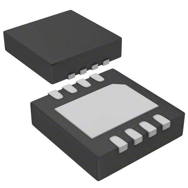
| 供应商器件封装 | 14-VQFN (3.5x3.5) |
| 其它名称 | 296-20703-6 |
| 制造商产品页 | http://www.ti.com/general/docs/suppproductinfo.tsp?distId=10&orderablePartNumber=DAC8831IBRGYT |
| 包装 | Digi-Reel® |
| 安装类型 | 表面贴装 |
| 封装/外壳 | 14-VFQFN 裸露焊盘 |
| 工作温度 | -40°C ~ 85°C |
| 建立时间 | 1µs |
| 数据接口 | 串行 |
| 标准包装 | 1 |
| 电压源 | 单电源 |
| 转换器数 | 1 |
| 输出数和类型 | 1 电压,单极1 电压,双极 |
| 配用 | /product-detail/zh/DAC8831EVM/296-20839-ND/1216444 |
| 采样率(每秒) | 2M |


PDF Datasheet 数据手册内容提取
(cid:2)(cid:10)(cid:14)(cid:17)(cid:13)(cid:14)(cid:11)(cid:14)(cid:20) (cid:2)(cid:5)(cid:9)(cid:14)(cid:13)(cid:19)(cid:18)(cid:6)(cid:15)(cid:12) (cid:3)(cid:4)(cid:12)(cid:15)(cid:14)(cid:13)(cid:16)(cid:14)(cid:8)(cid:17)(cid:17)(cid:11)(cid:7)(cid:9)(cid:16)(cid:15)(cid:12)(cid:16)(cid:15) IVC102 DAC8830 DAC8831 OPA132 DAC8831® SLAS449D–FEBRUARY2005–REVISEDSEPTEMBER2007 16-Bit, Ultra-Low Power, Voltage-Output Digital-to-Analog Converters FEATURES DESCRIPTION 1 • 16-BitResolution The DAC8830 and DAC8831 are single, 16-bit, 234 • 2.7Vto5.5VSingle-SupplyOperation serial-input, voltage-output digital-to-analog • VeryLowPower:15μWfor3VPower converters (DACs) operating from a single 3 V to 5 V power supply. These converters provide excellent • HighAccuracy,INL:1LSB linearity (1 LSB INL), low glitch, low noise, and fast • LowNoise:10nV/√Hz settling (1.0 μS to 1/2 LSB of full-scale output) over • FastSettling:1.0μS the specified temperature range of –40(cid:176) C to +85(cid:176) C. The output is unbuffered, which reduces the power • FastSPI™Interface,upto50MHz consumptionandtheerrorintroducedbythebuffer. • ResettoZero-Code These parts feature a standard high-speed (clock up • Schmitt-TriggerInputsforDirectOptocoupler to 50 MHz), 3 V or 5 V SPI serial interface to Interface communicatewithaDSPormicroprocessor. • Industry-StandardPinConfiguration The DAC8830 output is 0 V to V . However, the REF DAC8831 provides bipolar output (±V ) when APPLICATIONS REF working with an external buffer. The DAC8830 and • PortableEquipment DAC8831 are both reset to zero code after power up. • AutomaticTestEquipment For optimum performance, a set of Kelvin • IndustrialProcessControl connections to external reference and analog ground inputareprovidedontheDAC8831. • DataAcquisitionSystems • OpticalNetworking The DAC8830 is available in an SO-8 package, and the DAC8831 in an SO-14 package. Both have industry standard pinouts (see Table 3, the cross-reference table in the Application Information section for details). The DAC8831 is also available in aQFN-14package. DAC8830 DAC8831 FunctionalBlockDiagram FunctionalBlockDiagram VDD VDD VREF- S VREF- F RINV RFB RFB VREF DAC VOUT LDAC INV +V SCSCLDKSI SerialInterface ReIngpisutter DACLatch AGND SCSCLDKSI SerialInterfaceandControlLogic ReIngpisutter DADCALCatch AAVGGOUNNTDDSF+- - VOOOPPPAAA277702V747O DAC8830 DAC8831 DGND DGND 1 Pleasebeawarethatanimportantnoticeconcerningavailability,standardwarranty,anduseincriticalapplicationsof TexasInstrumentssemiconductorproductsanddisclaimerstheretoappearsattheendofthisdatasheet. SPI,QSPIaretrademarksofMotorola,Inc. 2 MicrowireisatrademarkofNationalSemiconductorCorp. 3 Allothertrademarksarethepropertyoftheirrespectiveowners. 4 PRODUCTIONDATAinformationiscurrentasofpublicationdate. Copyright©2005–2007,TexasInstrumentsIncorporated Products conform to specifications per the terms of the Texas Instruments standard warranty. Production processing does not necessarilyincludetestingofallparameters.
DAC8830 DAC8831 www.ti.com SLAS449D–FEBRUARY2005–REVISEDSEPTEMBER2007 This integrated circuit can be damaged by ESD. Texas Instruments recommends that all integrated circuits be handled with appropriateprecautions.Failuretoobserveproperhandlingandinstallationprocedurescancausedamage. ESDdamagecanrangefromsubtleperformancedegradationtocompletedevicefailure.Precisionintegratedcircuitsmaybemore susceptibletodamagebecauseverysmallparametricchangescouldcausethedevicenottomeetitspublishedspecifications. ORDERINGINFORMATION(1) MINIMUM POWER- RELATIVE DIFFERENTIAL ON SPECIFIED TRANSPORT ACCURACY NONLINEARITY RESET TEMPERATURE PACKAGE PACKAGE- PACKAGE ORDERING MEDIA, PRODUCT (LSB) (LSB) VALUE RANGE MARKING LEAD DESIGNATOR NUMBER QUANTITY DAC8830ID Tubes,75 DAC8830ID ±4 ±1 ZeroCode –40(cid:176)Cto+85(cid:176)C 8830I SO-8 D DAC8830IDR TapeandReel,2500 DAC8830IBD Tubes,75 DAC8830IBD ±2 ±1 ZeroCode –40(cid:176)Cto+85(cid:176)C 8830I SO-8 D DAC8830IBDR TapeandReel,2500 DAC8830ICD Tubes,75 DAC8830ICD ±1 ±1 ZeroCode –40(cid:176)Cto+85(cid:176)C 8830I SO-8 D DAC8830ICDR TapeandReel,2500 DAC8831ID Tube,50 DAC8831ID ±4 ±1 ZeroCode –40(cid:176)Cto+85(cid:176)C 8831I SO-14 D DAC8831IDR TapeandReel,2500 DAC8831IBD Tube,50 DAC8831IBD ±2 ±1 ZeroCode –40(cid:176)Cto+85(cid:176)C 8831I SO-14 D DAC8831IBDR TapeandReel,2500 DAC8831ICD Tube,50 DAC8831ICD ±1 ±1 ZeroCode –40(cid:176)Cto+85(cid:176)C 8831I SO-14 D DAC8831ICDR TapeandReel,2500 DAC8831IRGYT TapeandReel,250 DAC8831IRGY ±4 ±1 ZeroCode –40(cid:176)Cto+85(cid:176)C 8831I QFN-14 RGY DAC8831IRGYR TapeandReel,1000 DAC8831IBRGYT TapeandReel,250 DAC8831IBRGY ±2 ±1 ZeroCode –40(cid:176)Cto+85(cid:176)C 8831I QFN-14 RGY DAC8831IBRGYR TapeandReel,1000 DAC8831ICRGYT TapeandReel,250 DAC8831ICRGY ±1 ±1 ZeroCode –40(cid:176)Cto+85(cid:176)C 8831I QFN-14 RGY DAC8831ICRGYR TapeandReel,1000 (1) Forthemostcurrentpackageandorderinginformation,seethePackageOptionAddendumattheendofthisdatasheet,orseetheTI websiteatwww.ti.com. ABSOLUTE MAXIMUM RATINGS Overoperatingfree-airtemperaturerange(unlessotherwisenoted)(1) DAC8830,DAC8831 UNIT V toAGND –0.3to+7 V DD DigitalinputvoltagetoDGND –0.3to+V +0.3 V DD V toAGND –0.3to+V +0.3 V OUT DD AGND,AGNDF,AGNDStoDGND –0.3to+0.3 V Operatingtemperaturerange –40to+85 (cid:176) C Storagetemperaturerange –65to+150 (cid:176) C Junctiontemperaturerange(T max) +150 (cid:176) C J Powerdissipation (T max-T )/θ W J A JA QFN-14 54.9 (cid:176) C/W Thermalimpedance,θ SO-8 136.9 (cid:176) C/W JA SO-14 66.6 (cid:176) C/W (1) StressesabovethoselistedunderAbsoluteMaximumRatingsmaycausepermanentdamagetothedevice.Exposuretoabsolute maximumconditionsforextendedperiodsmayaffectdevicereliability. 2 SubmitDocumentationFeedback Copyright©2005–2007,TexasInstrumentsIncorporated ProductFolderLink(s):DAC8830DAC8831
DAC8830 DAC8831 www.ti.com SLAS449D–FEBRUARY2005–REVISEDSEPTEMBER2007 ELECTRICAL CHARACTERISTICS AllspecificationsatT =T toT ,V =+3VorV =+5V,V =+2.5Vunlessotherwisenoted. A MIN MAX DD DD REF DAC8830,DAC8831 PARAMETER CONDITIONS MIN TYP MAX UNIT STATICPERFORMANCE Resolution 16 bits DAC8830ICD, DAC8831ICD, ±0.5 ±1 DAC8831ICRGY DAC8830IBD, Linearityerror DAC8831IBD, ±0.5 ±2 LSB DAC8831IBRGY DAC8830ID, DAC8831ID, ±0.5 ±4 DAC8831IRGY Differentiallinearityerror Allgrades ±0.5 ±1 LSB TA=+25(cid:176)C ±1 ±5 Gainerror LSB TA=–40(cid:176)Cto+85(cid:176)C ±7 Gaindrift ±0.1 ppm/(cid:176)C TA=+25(cid:176)C ±0.25 ±1 Zerocodeerror LSB TA=–40(cid:176)Cto+85(cid:176)C ±2 Zerocodedrift ±0.05 ppm/(cid:176)C OUTPUTCHARACTERISTICS Voltageoutput(1) Alldevices Unipolaroperation 0 +VREF V DAC8831only Bipolaroperation –VREF +VREF V Outputimpedance 6.25 kΩ Settlingtime To1/2LSBofFS,CL=10pF 1 μs Slewrate(2) CL=10pF 25 V/μs Digital-to-analogglitch 1LSBchangearoundmajorcarry 35 nV-s Digitalfeedthrough(3) 0.2 nV-s DAC8830 10 Outputnoise TA=+25(cid:176)C nV/√Hz DAC8831 18 Power-supplyrejection VDDvaries±10% ±1 LSB Bipolarresistor RFB/RINV 1 Ω/Ω DAC8831only matching Ratioerror ±0.0015 ±0.0076 % TA=+25(cid:176)C ±0.25 ±5 Bipolarzeroerror DAC8831only LSB TA=–40(cid:176)Cto+85(cid:176)C ±7 Bipolarzerodrift DAC8831only ±0.2 ppm/(cid:176)C (1) TheDAC8830outputisunipolar(0Vto+V ).TheDAC8831outputisbipolar(±V )whenitconnectstoanexternalbuffer(seethe REF REF BipolarOutputOperationsectionfordetails). (2) Slewrateismeasuredfrom10%to90%oftransitionwhentheoutputchangesfrom0tofull-scale. (3) Digitalfeedthroughisdefinedastheimpulseinjectedintotheanalogoutputfromthedigitalinput.ItismeasuredwhentheDACoutput doesnotchange;CSisheldhigh,whileSCLKandDINsignalsaretoggled. Copyright©2005–2007,TexasInstrumentsIncorporated SubmitDocumentationFeedback 3 ProductFolderLink(s):DAC8830DAC8831
DAC8830 DAC8831 www.ti.com SLAS449D–FEBRUARY2005–REVISEDSEPTEMBER2007 ELECTRICAL CHARACTERISTICS (continued) AllspecificationsatT =T toT ,V =+3VorV =+5V,V =+2.5Vunlessotherwisenoted. A MIN MAX DD DD REF DAC8830,DAC8831 PARAMETER CONDITIONS MIN TYP MAX UNIT REFERENCEINPUT Referenceinputvoltagerange 1.25 VDD V Unipolarmode 9 Referenceinputimpedance(4) kΩ Bipolarmode,DAC8831 7.5 Reference–3dBbandwidth,BW Code=FFFFh 1.3 MHz Referencefeedthrough Code=0000h,VREF=1VPPat100kHz 1 mV Signal-to-noiseratio,SNR 92 dB Code=0000h 75 Referenceinputcapacitance pF Code=FFFFh 120 DIGITALINPUTS VDD=2.7V 0.6 VIL Inputlowvoltage V VDD=5V 0.8 VDD=2.7V 2.1 VIH Inputhighvoltage V VDD=5V 2.4 Inputcurrent ±1 μA Inputcapacitance 10 pF Hysteresisvoltage 0.4 V POWERSUPPLY VDD Power-supplyvoltage 2.7 5.5 V VDD=3V 5 20 IDD Power-supplycurrent μA VDD=5V 5 20 VDD=3V 15 60 Power μW VDD=5V 25 100 TEMPERATURERANGE Specifiedperformance –40 +85 (cid:176)C (4) Referenceinputresistanceiscode-dependent,minimumat8555h. 4 SubmitDocumentationFeedback Copyright©2005–2007,TexasInstrumentsIncorporated ProductFolderLink(s):DAC8830DAC8831
DAC8830 DAC8831 www.ti.com SLAS449D–FEBRUARY2005–REVISEDSEPTEMBER2007 PIN CONFIGURATIONS (NOT TO SCALE) DPACKAGE DPACKAGE RGYPACKAGE SO-8 SO-14 QFN-14 (TOPVIEW) (TOPVIEW) (TOPVIEW) D C AGVONUDT 12 8830 87 VDDGDND VROFUBT 12 1 1143 VINDVD 1INV3 1DGN2 1LDA1 1SDI0 NC9 V 3 C 6 SDI AGNDF 3 3 12 DGND REF A 8 CS 4 D 5 SCLK AGNDS 4 C8 11 LDAC A V 14 8 SCLK VREF−S 5 D 10 SDI DD V −F 6 9 NC REF DAC8831 CS 7 8 SCLK ThermalPad(1) RFB 1 7 CS 2 3 4 5 6 VOUT GNDF GNDS -SREF -FREF A A V V NOTE:(1)ExposedthermalpadintheQFNpackage mustbeconnectedtoanalogground. TERMINALFUNCTIONS TERMINAL DESCRIPTION NO. NAME DAC8830 1 V AnalogoutputofDAC OUT 2 AGND Analogground 3 V Voltagereferenceinput REF 4 CS Chipselectinput(activelow).DataarenotclockedintoSDIunlessCSislow 5 SCLK Serialclockinput 6 SDI Serialdatainput.DataarelatchedintoinputregisterontherisingedgeofSCLK. 7 DGND Digitalground 8 V Analogpowersupply,+3Vto+5V DD DAC8831 1 RFB Feedbackresistor.Connecttotheoutputofexternaloperationalamplifierinbipolarmode. 2 V AnalogoutputofDAC OUT 3 AGNDF Analogground(Force) 4 AGNDS Analogground(Sense) 5 V S Voltagereferenceinput(Sense).Connecttoexternalvoltagereference REF– 6 V F Voltagereferenceinput(Force).Connecttoexternalvoltagereference REF– 7 CS Chipselectinput(activelow).DataarenotclockedintoSDIunlessCSislow. 8 SCLK Serialclockinput. 9 NC Nointernalconnection 10 SDI Serialdatainput.DataarelatchedintoinputregisterontherisingedgeofSCLK. LoadDACcontrolinput.Activelow.WhenLDACisLow,theDAClatchissimultaneouslyupdatedwiththecontent 11 LDAC oftheinputregister. 12 DGND Digitalground 13 INV Junctionpointofinternalscalingresistors.Connecttoexternaloperationalamplifierinvertinginputinbipolarmode. 14 V Analogpowersupply,+3Vto+5V. DD Copyright©2005–2007,TexasInstrumentsIncorporated SubmitDocumentationFeedback 5 ProductFolderLink(s):DAC8830DAC8831
DAC8830 DAC8831 www.ti.com SLAS449D–FEBRUARY2005–REVISEDSEPTEMBER2007 ttd CS DAC Updated tDelay tsck tLead twsck twsck tLag tDSCLK SCLK tsu tho SDI BIT15 (MSB) BIT14 BIT13, . . . ,1 BIT0 --- Don't Care Figure1.DAC8830TimingDiagram Case1: LDACtied to LOW ttd CS DAC Updated tDelay tsck tLead twsck twsck tLag tDSCLK SCLK tsu tho SDI BIT15 (MSB) BIT14 BIT13, . . . ,1 BIT0 LDAC LOW −−−Don’t Care Case2: LDACActive ttd CS tDelay tsck tLead twsck twsck tLag tDSCLK SCLK tsu tho SDI BIT15 (MSB) BIT14 BIT13, . . . ,1 BIT0 HIGH tDLADC tWLDAC LDAC DAC Updated −−−Don’t Care Figure2.DAC8831TimingDiagram 6 SubmitDocumentationFeedback Copyright©2005–2007,TexasInstrumentsIncorporated ProductFolderLink(s):DAC8830DAC8831
DAC8830 DAC8831 www.ti.com SLAS449D–FEBRUARY2005–REVISEDSEPTEMBER2007 TIMING CHARACTERISTICS: V = +5 V(1)(2) DD At–40(cid:176) Cto+85(cid:176) C,unlessotherwisenoted. PARAMETER MIN MAX UNIT t SCLKperiod 20 ns sck t SCLKhighorlowtime 10 ns wsck t DelayfromSCLKhightoCSlow 10 ns Delay t CSenableleadtime 10 ns Lead t CSenablelagtime 10 ns Lag t DelayfromCShightoSCLKhigh 10 ns DSCLK t CShighbetweenactiveperiod 30 ns td t Datasetuptime(input) 10 ns su t Dataholdtime(input) 0 ns ho t LDACwidth 30 ns WLDAC t DelayfromCShightoLDAClow 30 ns DLDAC V hightoCSlow(power-updelay) 10 μs DD (1) Assuredbydesign.Notproductiontested. (2) Sampletestedduringtheinitialreleaseandafteranyredesignorprocesschangesthatmayaffectthisparameter. TIMING CHARACTERISTICS: V = +3 V(1)(2) DD At–40(cid:176) Cto+85(cid:176) C,unlessotherwisenoted. PARAMETER MIN MAX UNIT t SCLKperiod 20 ns sck t SCLKhighorlowtime 10 ns wsck t DelayfromSCLKhightoCSlow 10 ns Delay t CSenableleadtime 10 ns Lead t CSenablelagtime 10 ns Lag t DelayfromCShightoSCLKhigh 10 ns DSCLK t CShighbetweenactiveperiod 30 ns td t Datasetuptime(input) 10 ns su t Dataholdtime(input) 0 ns ho t LDACwidth 30 ns WLDAC t DelayfromCShightoLDAClow 30 ns DLDAC V hightoCSlow(power-updelay) 10 μs DD (1) Assuredbydesign.Notproductiontested. (2) Sampletestedduringtheinitialreleaseandafteranyredesignorprocesschangesthatmayaffectthisparameter. Copyright©2005–2007,TexasInstrumentsIncorporated SubmitDocumentationFeedback 7 ProductFolderLink(s):DAC8830DAC8831
DAC8830 DAC8831 www.ti.com SLAS449D–FEBRUARY2005–REVISEDSEPTEMBER2007 TYPICAL CHARACTERISTICS: V = +5 V DD AtT =+25(cid:176) CandV =+2.5V,unlessotherwisenoted. A REF LINEARITYERROR DIFFERENTIALLINEARITYERROR vsDIGITALINPUTCODE vsDIGITALINPUTCODE 1.00 1.00 0.75 TA=+25(cid:1)C 0.75 TA=+25(cid:1)C VREF=2.5 V VREF=2.5 V 0.50 0.50 B) 0.25 B) 0.25 S S INL(L - 0.205 DNL(L - 0.205 - 0.50 - 0.50 - 0.75 - 0.75 - 1.00 - 1.00 0 8192 16384 24576 32768 40960 49152 57344 65536 0 8192 16384 24576 32768 40960 49152 57344 65536 DigitalInputCode DigitalInputCode Figure3. Figure4. LINEARITYERROR DIFFERENTIALLINEARITYERROR vsDIGITALINPUTCODE vsDIGITALINPUTCODE 1.00 1.00 T =- 40(cid:1)C T =- 40(cid:1)C 0.75 A 0.75 A V =2.5 V V =2.5 V REF REF 0.50 0.50 B) 0.25 B) 0.25 S S INL(L - 0.205 DNL(L - 0.205 - 0.50 - 0.50 - 0.75 - 0.75 - 1.00 - 1.00 0 8192 16384 24576 32768 40960 49152 57344 65536 0 8192 16384 24576 32768 40960 49152 57344 65536 DigitalInputCode DigitalInputCode Figure5. Figure6. LINEARITYERROR DIFFERENTIALLINEARYERROR vsDIGITALINPUTCODE vsDIGITALINPUTCODE 1.00 1.00 T =+85(cid:1)C T =+85(cid:1)C 0.75 A 0.75 A V =2.5 V V =2.5 V REF REF 0.50 0.50 INL(LSB) - 00..22505 DNL(LSB) - 00..22505 - 0.50 - 0.50 - 0.75 - 0.75 - 1.00 - 1.00 0 8192 16384 24576 32768 40960 49152 57344 65536 0 8192 16384 24576 32768 40960 49152 57344 65536 DigitalInputCode DigitalInputCode Figure7. Figure8. 8 SubmitDocumentationFeedback Copyright©2005–2007,TexasInstrumentsIncorporated ProductFolderLink(s):DAC8830DAC8831
DAC8830 DAC8831 www.ti.com SLAS449D–FEBRUARY2005–REVISEDSEPTEMBER2007 TYPICAL CHARACTERISTICS: V = +5 V (continued) DD AtT =+25(cid:176) CandV =+2.5V,unlessotherwisenoted. A REF LINEARITYERROR DIFFERENTIALLINEARITYERROR vsDIGITALINPUTCODE vsDIGITALINPUTCODE 1.00 1.00 T =+25(cid:1)C T =+25(cid:1)C 0.75 A 0.75 A V =5 V V =5 V REF REF 0.50 0.50 B) 0.25 B) 0.25 S S INL(L - 0.205 DNL(L - 0.205 - 0.50 - 0.50 - 0.75 - 0.75 - 1.00 - 1.00 0 8192 16384 24576 3276840960 49152 57344 65536 0 8192 16384 24576 32768 40960 49152 57344 65536 DigitalInputCode DigitalInputCode Figure9. Figure10. LINEARITYERROR LINEARITYERROR vsREFERENCEVOLTAGE vsSUPPLYVOLTAGE 0.75 0.75 V =2.5 V REF 0.50 0.50 B) B) S S L L DNL ( 0.25 DNL ( 0.25 or or Err Err y y arit 0 INL arit 0 e e INL n n Li Li - 0.25 - 0.25 - 0.50 - 0.50 0 1 2 3 4 5 6 2.5 3.0 3.5 4.0 4.5 5.0 5.5 6.0 ReferenceVoltage(V) SupplyVoltage(V) Figure11. Figure12. GAINERROR ZERO-CODEERROR vsTEMPERATURE vsTEMPERATURE 1.25 0.50 BipolarMode V =2.5 V 1.00 REF 0.75 B) 0.25 S B) L BipolarMode LS 0.50 or( or( 0.25 Err 0 Err de Gain 0 UnipolarMode o−Co - 0.25 er - 0.25 Z - 0.50 UnipolarMode V =2.5 V - 0.75 REF - 0.50 - 60 - 40 - 20 0 20 40 60 80 100 120 140 - 60 - 40 - 20 0 20 40 60 80 100 120 140 Temperature((cid:1)C) Temperature((cid:1)C) Figure13. Figure14. Copyright©2005–2007,TexasInstrumentsIncorporated SubmitDocumentationFeedback 9 ProductFolderLink(s):DAC8830DAC8831
DAC8830 DAC8831 www.ti.com SLAS449D–FEBRUARY2005–REVISEDSEPTEMBER2007 TYPICAL CHARACTERISTICS: V = +5 V (continued) DD AtT =+25(cid:176) CandV =+2.5V,unlessotherwisenoted. A REF REFERENCECURRENT REFERENCECURRENT vsCODE(UNIPOLARMODE) vsCODE(BIPOLARMODE) 300 300 V =2.5 V V =2.5 V REF REF 250 250 A) A) m( 200 m( 200 nt nt e e Curr 150 Curr 150 e e c c n n ere 100 ere 100 ef ef R R 50 50 0 0 0 8192 16384 24576 3276840960 49152 57344 65536 0 8192 16384 24576 3276840960 49152 57344 65536 DigitalInputCode DigitalInputCode Figure15. Figure16. SUPPLYCURRENT SUPPLYCURRENT vsDIGITALINPUTVOLTAGE vsTEMPERATURE 800 5 V =2.5 V 700 REF VDD=5 V 4 600 V =5 V A) A) VDD =5 V m( 500 m( LOGIC nt nt 3 e e urr 400 urr C C V =3 V Supply 320000 VDD=3 V Supply 2 VDLODGIC=3 V 1 100 0 0 0 1 2 3 4 5 - 60 - 40 - 20 0 20 40 60 80 100 120 140 DigitalInputVoltage(V) Temperature((cid:1)C) Figure17. Figure18. SUPPLYCURRENT SUPPLYCURRENT vsSUPPLYVOLTAGE vsREFERENCEVOLTAGE 5.0 5.0 V =2.5 V 4.5 REF 4.5 4.0 4.0 A) 3.5 A) 3.5 V =5 V m( m( DD nt 3.0 nt 3.0 e e urr 2.5 urr 2.5 C C y 2.0 y 2.0 pl pl V =3 V p p DD u 1.5 u 1.5 S S 1.0 1.0 0.5 0.5 0 0 2.7 3.0 3.3 3.6 3.9 4.2 4.5 4.8 5.1 5.4 5.7 6.0 0 0.5 1.0 1.5 2.0 2.5 3.0 3.5 4.0 4.5 5.0 SupplyVoltage(V) ReferenceVoltage(V) Figure19. Figure20. 10 SubmitDocumentationFeedback Copyright©2005–2007,TexasInstrumentsIncorporated ProductFolderLink(s):DAC8830DAC8831
DAC8830 DAC8831 www.ti.com SLAS449D–FEBRUARY2005–REVISEDSEPTEMBER2007 TYPICAL CHARACTERISTICS: V = +5 V (continued) DD AtT =+25(cid:176) CandV =+2.5V,unlessotherwisenoted. A REF MAJOR-CARRYGLITCH MAJOR-CARRYGLITCH (FALLING) (RISING) V = 2.5V V = 2.5V 5V/div REF 5V/div REF LDAC LDAC V V OUT OUT 0.1V/div 0.1V/div Time (0.5ms/div) Time (0.5ms/div) Figure21. Figure22. DACSETTLINGTIME DACSETTLINGTIME (FALLING) (RISING) V = 2.5V V = 2.5V 5V/div REF 5V/div REF LDAC LDAC 1V/div V OUT VOUT 1V/div Time (0.2ms/div) Time (0.2ms/div) Figure23. Figure24. DIGITAL FEEDTHROUGH V =2.5 V REF SDI 5V/div V 20mV/div OUT Time(50ns/div) Figure25. Copyright©2005–2007,TexasInstrumentsIncorporated SubmitDocumentationFeedback 11 ProductFolderLink(s):DAC8830DAC8831
DAC8830 DAC8831 www.ti.com SLAS449D–FEBRUARY2005–REVISEDSEPTEMBER2007 TYPICAL CHARACTERISTICS: V = +3 V DD AtT =+25(cid:176) CandV =+2.5V,unlessotherwisenoted. A REF LINEARITYERROR DIFFERENTIALLINEARITYERROR vsDIGITALINPUTCODE vsDIGITALINPUTCODE 1.00 1.00 T =+25(cid:1)C T =+25(cid:1)C 0.75 A 0.75 A V =1.5 V V =1.5 V REF REF 0.50 0.50 B) 0.25 B) 0.25 S S INL(L - 0.205 DNL(L - 0.205 - 0.50 - 0.50 - 0.75 - 0.75 - 1.00 - 1.00 0 8192 16384 24576 32768 40960 49152 57344 65536 0 8192 16384 24576 32768 40960 49152 57344 65536 DigitalInputCode DigitalInputCode Figure26. Figure27. LINEARITYERROR DIFFERENTIALLINEARITYERROR vsDIGITALINPUTCODE vsDIGITALINPUTCODE 1.00 1.00 T =- 40(cid:1)C T =- 40(cid:1)C 0.75 A 0.75 A V =1.5 V V =1.5 V REF REF 0.50 0.50 B) 0.25 B) 0.25 S S INL(L - 0.205 DNL(L - 0.205 - 0.50 - 0.50 - 0.75 - 0.75 - 1.00 - 1.00 0 8192 16384 24576 32768 40960 49152 57344 65536 0 8192 16384 24576 32768 40960 49152 57344 65536 DigitalInputCode DigitalInputCode Figure28. Figure29. LINEARITYERROR DIFFERENTIALLINEARYERROR vsDIGITALINPUTCODE vsDIGITALINPUTCODE 1.00 1.00 T =+85(cid:1)C T =+85(cid:1)C 0.75 A 0.75 A V =1.5 V V =1.5 V REF REF 0.50 0.50 B) 0.25 B) 0.25 S S INL(L - 0.205 DNL(L - 0.205 - 0.50 - 0.50 - 0.75 - 0.75 - 1.00 - 1.00 0 8192 16384 24576 32768 40960 49152 57344 65536 0 8192 16384 24576 32768 40960 49152 57344 65536 DigitalInputCode DigitalInputCode Figure30. Figure31. 12 SubmitDocumentationFeedback Copyright©2005–2007,TexasInstrumentsIncorporated ProductFolderLink(s):DAC8830DAC8831
DAC8830 DAC8831 www.ti.com SLAS449D–FEBRUARY2005–REVISEDSEPTEMBER2007 TYPICAL CHARACTERISTICS: V = +3 V (continued) DD AtT =+25(cid:176) CandV =+2.5V,unlessotherwisenoted. A REF LINEARITYERROR DIFFERENTIALLINEARITYERROR vsDIGITALINPUTCODE vsDIGITALINPUTCODE 1.00 1.00 T =+25(cid:1)C T =+25(cid:1)C 0.75 A 0.75 A V =3 V V =3 V REF REF 0.50 0.50 INL(LSB) - 00..22505 DNL(LSB) - 00..22505 - 0.50 - 0.50 - 0.75 - 0.75 - 1.00 - 1.00 0 8192 16384 24576 3276840960 49152 57344 65536 0 8192 16384 24576 32768 40960 49152 57344 65536 DigitalInputCode DigitalInputCode Figure32. Figure33. LINEARITYERROR GAINERROR vsREFERENCEVOLTAGE vsTEMPERATURE 0.75 1.00 0.75 BipolarMode 0.50 0.50 B) or(LS 0.25 DNL (LSB) 0.25 yErr Error 0 UnipolarMode nearit 0 Gain - 0.25 Li - 0.50 - 0.25 V =3 V - 0.75 DD INL V =2.5 V REF - 0.50 - 1.00 0.5 1.0 1.5 2.0 2.5 3.0 3.5 - 60 - 40 - 20 0 20 40 60 80 100 120 140 ReferenceVoltage(V) Temperature((cid:1)C) Figure34. Figure35. ZERO-CODEERROR REFERENCECURRENT vsTEMPERATURE vsCODE(UNIPOLARMODE) 0.50 300 VDD=3 V VREF=1.5 V V =2.5 V REF 250 0.25 B) A) S L m( 200 Error( 0 UnipolarMode Current 150 e od - 0.25 ce C n o− BipolarMode ere 100 er ef Z - 0.50 R 50 - 0.75 0 - 60 - 40 - 20 0 20 40 60 80 100 120 140 0 8192 16384 24576 3276840960 49152 57344 65536 Temperature((cid:1)C) DigitalInputCode Figure36. Figure37. Copyright©2005–2007,TexasInstrumentsIncorporated SubmitDocumentationFeedback 13 ProductFolderLink(s):DAC8830DAC8831
DAC8830 DAC8831 www.ti.com SLAS449D–FEBRUARY2005–REVISEDSEPTEMBER2007 TYPICAL CHARACTERISTICS: V = +3 V (continued) DD AtT =+25(cid:176) CandV =+2.5V,unlessotherwisenoted. A REF REFERENCECURRENT DIGITAL vsCODE(BIPOLARMODE) FEEDTHROUGH 300 VREF=1.5 V VREF=2.5 V 250 SDI A) 5V/div m( 200 nt e Curr 150 ce 20mV/div VOUT n ere 100 ef R 50 0 Time(50ns/div) 0 8192 16384 24576 3276840960 49152 57344 65536 DigitalInputCode Figure38. Figure39. MAJOR-CARRYGLITCH MAJOR-CARRYGLITCH (FALLING) (RISING) V = 2.5V V = 2.5V REF REF 5V/div LDAC 5V/div LDAC V V OUT OUT 0.1V/div 0.1V/div Time (0.5ms/div) Time (0.5ms/div) Figure40. Figure41. DACSETTLINGTIME DACSETTLINGTIME (FALLING) (RISING) V = 2.5V V = 2.5V REF REF 5V/div LDAC 5V/div LDAC 1V/div V OUT VOUT 1V/div Time (0.2ms/div) Time (0.2ms/div) Figure42. Figure43. THEORY OF OPERATION GENERAL DESCRIPTION The DAC8830 and DAC8831 are single, 16-bit, serial-input, voltage-output DACs. They operate from a single 14 SubmitDocumentationFeedback Copyright©2005–2007,TexasInstrumentsIncorporated ProductFolderLink(s):DAC8830DAC8831
DAC8830 DAC8831 www.ti.com SLAS449D–FEBRUARY2005–REVISEDSEPTEMBER2007 supply ranging from 2.7 V to 5 V, and typically consume 5 μA. Data are written to these devices in a 16-bit word format, via an SPI serial interface. To ensure a known power-up state, these parts are designed with a power-on reset function. The DAC8830 and DAC8831 are reset to zero code. In unipolar mode, the DAC8830 and DAC8831areresetto0V,and in bipolar mode, the DAC8831 is reset to –V . Kelvin sense connections for the REF referenceandanaloggroundareincludedontheDAC8831. DIGITAL-TO-ANALOG SECTIONS The DAC architecture for both devices consists of two matched DAC sections and is segmented. A simplified circuit diagram is shown in Figure 44. The four MSBs of the 16-bit data word are decoded to drive 15 switches, E1 to E15. Each of these switches connects one of 15 matched resistors to either AGND or V . The remaining REF 12bitsofthedataworddriveswitchesS0toS11ofa12-bitvoltagemodeR-2Rladdernetwork. R R V OUT 2R 2R 2R 2R 2R 2R 2R S0 S1 S11 E1 E2 E15 V REF 12−BitR−2RLadder FourMSBsDecodedinto 15EqualSegments Figure44.DACArchitecture OUTPUT RANGE TheoutputoftheDACis V =(V · Code)/65536. OUT REF WhereCodeisthedecimaldatawordloadedtotheDAClatch. Copyright©2005–2007,TexasInstrumentsIncorporated SubmitDocumentationFeedback 15 ProductFolderLink(s):DAC8830DAC8831
DAC8830 DAC8831 www.ti.com SLAS449D–FEBRUARY2005–REVISEDSEPTEMBER2007 POWER-ON RESET Both devices have a power-on reset function to ensure the output is at a known state upon power-up. In the DAC8830andDAC8831,atpower-up,theDAClatchandInputRegisterscontainall0suntilnew data are loaded from the input serial shift register. Therefore, after power-up, the output from pin V of the DAC8830 is 0 V. OUT TheoutputfrompinV oftheDAC8831is0Vinunipolarmodeand–V inbipolarmode. OUT REF However, the serial register of the DAC8830 and DAC8831 is not cleared on power-up, so its contents are undefined. When loading data initially to the device, 16 bits or more should be loaded to prevent erroneous data appearing on the output. If more than 16 bits are loaded, the last 16 are kept; if less than 16 are loaded, bits will remainfromthepreviousword.Ifthedevicemustbeinterfaced with data shorter than 16 bits, the data should be paddedwith0sattheLSBs. Serial Interface The digital interface is a standard 3-wire connection compatible with SPI, QSPI™, Microwire™, and TI DSP interfaces, which can operate at speeds up to 50 M-bits/sec. The data transfer is framed by CS, the chip select signal. The DAC works as a bus slave. The bus master generates the synchronize clock, SCLK, and initiates the transmission. When CS is high, the DAC is not accessed, and the clock SCLK and serial input data SDI are ignored. The bus master accesses the DAC by driving pin CS low. Immediately following the high-to-low transition of CS, the serial input data on pin SDI is shifted out from the bus master synchronously on the falling edge of SCLK, and latched on the rising edge of SCLK into the input shift register, MSB first. The low-to-high transition of CS transfers the contents of the input shift register to the input register. All data registers are 16-bit. It takes 16 clocks of SCLK to transfer one data word to the parts. To complete a whole data word, CS must go high immediately after 16 SCLKs are clocked in. If more than 16 SCLKs are applied during the low state of CS, the last 16 bits are transferred to the input register on the rising edge of CS. However, if CS is not kept low duringtheentire16SCLKcycles,dataiscorrupted.Inthiscase,reloadtheDACwithanew16-bitword. In the DAC8830, the contents of the input register are transferred into the DAC latch immediately when the input registerisloaded,andtheDACoutputisupdatedatthesametime. The DAC8831 has an LDAC pin allowing the DAC latch to be updated asynchronously by bringing LDAC low after CS goes high. In this case, LDAC must be maintained high while CS is low. If LDAC is tied permanently low, the DAC latch is updated immediately after the input register is loaded (caused by the low-to-high transition ofCS). 16 SubmitDocumentationFeedback Copyright©2005–2007,TexasInstrumentsIncorporated ProductFolderLink(s):DAC8830DAC8831
DAC8830 DAC8831 www.ti.com SLAS449D–FEBRUARY2005–REVISEDSEPTEMBER2007 APPLICATION INFORMATION Unipolar Output Operation These DACs are capable of driving unbuffered loads of 60 kΩ. Unbuffered operation results in low supply current (typically 5 μA) and a low offset error. The DAC8830 provides a unipolar output swing ranging from 0 V to V . REF The DAC8831 can be configured to output both unipolar and bipolar voltages. Figure 45 and Figure 46 show a typical unipolar output voltage circuit for each device, respectively. The code table for this mode of operation is showninTable1. Table1.UnipolarCode DACLATCHCONTENTS MSB LSB ANALOGOUTPUT 1111111111111111 V · (65,535/65,536) REF 1000000000000000 V · (32,768/65,536)=1/2V REF REF 0000000000000001 V · (1/65,536) REF 0000000000000000 0V +5V +2.5V + 0.1m F 0.1m F 10m F OPA277 OPA704 OPA727 V V DD REF VOUT VO=0to+VREF DAC CS AGND e SCLK SerialInterfac RIengpisutter DACLatch SDI DAC8830 DGND Figure45.UnipolarOutputModeofDAC8830 Copyright©2005–2007,TexasInstrumentsIncorporated SubmitDocumentationFeedback 17 ProductFolderLink(s):DAC8830DAC8831
DAC8830 DAC8831 www.ti.com SLAS449D–FEBRUARY2005–REVISEDSEPTEMBER2007 +5V +2.5V + 0.1m F 0.1m F 10m F OPA277 VDD VREF- S VREF- F OPA704 OPA727 R R INV FB RFB +V LDAC SCCLKS erialInterfacedControlLogic Input DAC AIAVNGGOVUNNTDDSF - V VO=0to+VREF SDI San Register DACLatch DAC8831 DGND Figure46.UnipolarOutputModeofDAC8831 Assumingaperfectreference,theworst-caseoutputvoltagemaybecalculatedfromthefollowingequation: UnipolarModeWorst-CaseOutput D VOUT_UNI(cid:3)216(cid:1)(cid:4)VREF(cid:2)VGE(cid:5)(cid:2)VZSE(cid:2)INL Where: V =Unipolarmodeworst-caseoutput OUT_UNI D=CodeloadedtoDAC V =Referencevoltageappliedtopart REF V =Gainerrorinvolts GE V =Zero-scaleerrorinvolts ZSE INL=Integralnonlinearityinvolts 18 SubmitDocumentationFeedback Copyright©2005–2007,TexasInstrumentsIncorporated ProductFolderLink(s):DAC8830DAC8831
DAC8830 DAC8831 www.ti.com SLAS449D–FEBRUARY2005–REVISEDSEPTEMBER2007 Bipolar Output Operation With the aid of an external operational amplifier, the DAC8831 may be configured to provide a bipolar voltage output. A typical circuit of such an operation is shown in Figure 47. The matched bipolar offset resistors R and FB R are connected to an external operational amplifier to achieve this bipolar output swing; typically, R = R INV FB INV =28kΩ. +5V +2.5V + 0.1m F 0.1m F 10m F V V - S V - F DD REF REF R R INV FB RFB +V INV LDAC SCSCLDSKI SerialInterfaceandControlLogic ReIngpisutter DADCACLatch AAVGGOUNNTDDFS - V OOOPPPAAA277702747 VO=- VREFto+VREF DAC8831 DGND Figure47.BipolarOutputModeofDAC8831 Table 2 shows the transfer function for this output operating mode. The DAC8831 also provides a set of Kelvin connectionstotheanaloggroundandexternalreferenceinputs. Table2.BipolarCode DACLATCHCONTENTS MSB LSB ANALOGOUTPUT 1111111111111111 +V · (32,767/32,768) REF 1000000000000001 +V · (1/32,768) REF 1000000000000000 0V 0111111111111111 –V · (1/32,768) REF 0000000000000000 –V · (32,768/32,768)=–V REF REF Assumingaperfectreference,theworst-caseoutputvoltagemaybecalculatedfromthefollowingequation: BipolarModeWorst-CaseOutput (cid:4)(cid:6)VOUT_UNI(cid:1)VOS(cid:7)(2(cid:1)RD)(cid:2)VREF(1(cid:1)RD)(cid:5) VOUT_BIP(cid:3) 1(cid:1)(cid:6)2(cid:1)RD(cid:7) A Where: V =Externaloperationalamplifierinputoffsetvoltage OS RD=R andR resistormatchingerror FB IN A=Operationalamplifieropen-loopgain Copyright©2005–2007,TexasInstrumentsIncorporated SubmitDocumentationFeedback 19 ProductFolderLink(s):DAC8830DAC8831
DAC8830 DAC8831 www.ti.com SLAS449D–FEBRUARY2005–REVISEDSEPTEMBER2007 Output Amplifier Selection For bipolar mode, a precision amplifier should be used, supplied from a dual power supply. This provides the ±V output. REF In a single-supply application, selection of a suitable operational amplifier may be more difficult because the outputswingoftheamplifierdoesnotusuallyincludethenegativerail;inthiscase,AGND.Thisoutputswing can resultinsomedegradationofthespecifiedperformanceunlesstheapplicationdoesnotusecodesnear0. The selected operational amplifier needs to have low-offset voltage (the DAC LSB is 38 μV with a 2.5 V reference), eliminating the need for output offset trims. Input bias current should also be low because the bias currentmultipliedbytheDACoutputimpedance(approximately6.25kΩ)addstothezero-codeerror. Rail-to-rail input and output performance are required. For fast settling, the slew rate of the operational amplifier should not impede the settling time of the DAC. Output impedance of the DAC is constant and code-independent, but in order to minimize gain errors the input impedance of the output amplifier should be as high as possible. The amplifier should also have a 3 dB bandwidth of 1 MHz or greater. The amplifier adds another time constant to the system, thus increasing the settling time of the output. A higher 3 dB amplifier bandwidthresultsinashortereffectivesettlingtimeofthecombinedDACandamplifier. Reference and Ground Since the input impedance is code-dependent, the reference pin should be driven from a low impedance source. The DAC8830 and DAC8831 operate with a voltage reference ranging from 1.25 V to V . References below DD 1.25Vresultinreducedaccuracy. The DAC full-scale output voltage is determined by the reference. Table 1 and Table 2 outline the analog output voltageforparticulardigitalcodes. For optimum performance, Kelvin sense connections are provided on the DAC8831. If the application does not require separate force and sense lines, they should be tied together close to the package to minimize voltage dropsbetweenthepackageleadsandtheinternaldie. Power Supply and Reference Bypassing For accurate high-resolution performance, it is recommended that the reference and supply pins be bypassed witha10μFtantalumcapacitorinparallelwitha0.1μFceramiccapacitor. 20 SubmitDocumentationFeedback Copyright©2005–2007,TexasInstrumentsIncorporated ProductFolderLink(s):DAC8830DAC8831
DAC8830 DAC8831 www.ti.com SLAS449D–FEBRUARY2005–REVISEDSEPTEMBER2007 CROSS-REFERENCE TheDAC8830andDAC8831haveanindustry-standardpinoutconfiguration(seeTable3). Table3.Cross-Reference INL DNL POWER-ON TEMPERATURE PACKAGE PACKAGE CROSS MODEL (LSB) (LSB) RESETTO RANGE DESCRIPTION OPTION REFERENCE DAC8830ICD ±1 ±1 ZeroCode –40(cid:176)Cto+85(cid:176)C 8-LeadSmallOutlineIC SO-8 AD5541CR, MAX541AESA DAC8830IBD ±2 ±1 ZeroCode –40(cid:176)Cto+85(cid:176)C 8-LeadSmallOutlineIC SO-8 AD5541BR, MAX541BESA DAC8830ID ±4 ±1 ZeroCode –40(cid:176)Cto+85(cid:176)C 8-LeadSmallOutlineIC SO-8 AD5541AR, MAX541CESA N/A ±1 ±1 ZeroCode –40(cid:176)Cto+85(cid:176)C 8-LeadPlasticDIP PDIP-8 MAX541AEPA N/A ±2 ±1 ZeroCode –40(cid:176)Cto+85(cid:176)C 8-LeadPlasticDIP PDIP-8 MAX541BEPA N/A ±4 ±1 ZeroCode –40(cid:176)Cto+85(cid:176)C 8-LeadPlasticDIP PDIP-8 MAX541CEPA N/A ±1 ±1 ZeroCode 0(cid:176)Cto+70(cid:176)C 8-LeadSmallOutlineIC SO-8 AD5541LR N/A ±2 ±1.5 ZeroCode 0(cid:176)Cto+70(cid:176)C 8-LeadSmallOutlineIC SO-8 AD5541JR N/A ±1 ±1 ZeroCode 0(cid:176)Cto+70(cid:176)C 8-LeadPlasticDIP PDIP-8 MAX541AEPA N/A ±2 ±1 ZeroCode 0(cid:176)Cto+70(cid:176)C 8-LeadPlasticDIP PDIP-8 MAX541BEPA N/A ±4 ±1 ZeroCode 0(cid:176)Cto+70(cid:176)C 8-LeadPlasticDIP PDIP-8 MAX541CEPA DAC8831ICD ±1 ±1 ZeroCode –40(cid:176)Cto+85(cid:176)C 14-LeadSmallOutlineIC SO-14 AD5542CR, MAX542AESD DAC8831IBD ±2 ±1 ZeroCode –40(cid:176)Cto+85(cid:176)C 14-LeadSmallOutlineIC SO-14 AD5542BR, MAX542BESD DAC8831ID ±4 ±1 ZeroCode –40(cid:176)Cto+85(cid:176)C 14-LeadSmallOutlineIC SO-14 AD5542AR, MAX542CESD DAC8831ICRGY ±1 ±1 ZeroCode –40(cid:176)Cto+85(cid:176)C 14-LeadQFN QFN-14 N/A DAC8831IBRGY ±2 ±1 ZeroCode –40(cid:176)Cto+85(cid:176)C 14-LeadQFN QFN-14 N/A DAC8831IRGY ±4 ±1 ZeroCode –40(cid:176)Cto+85(cid:176)C 14-LeadQFN QFN-14 N/A N/A ±1 ±1 ZeroCode –40(cid:176)Cto+85(cid:176)C 14-LeadPlasticDIP PDIP-14 MAX542ACPD N/A ±2 ±1 ZeroCode –40(cid:176)Cto+85(cid:176)C 14-LeadPlasticDIP PDIP-14 MAX542BCPD N/A ±4 ±1 ZeroCode –40(cid:176)Cto+85(cid:176)C 14-LeadPlasticDIP PDIP-14 MAX542CCPD N/A ±1 ±1 ZeroCode 0(cid:176)Cto+70(cid:176)C 14-LeadSmallOutlineIC SO-14 AD5542LR N/A ±2 ±1.5 ZeroCode 0(cid:176)Cto+70(cid:176)C 14-LeadSmallOutlineIC SO-14 AD5542JR N/A ±1 ±1 ZeroCode 0(cid:176)Cto+70(cid:176)C 14-LeadSmallOutlineIC SO-14 MAX542AEPD N/A ±2 ±1 ZeroCode 0(cid:176)Cto+70(cid:176)C 14-LeadSmallOutlineIC SO-14 MAX542BEPD N/A ±4 ±1 ZeroCode 0(cid:176)Cto+70(cid:176)C 14-LeadSmallOutlineIC SO-14 MAX542CEPD Copyright©2005–2007,TexasInstrumentsIncorporated SubmitDocumentationFeedback 21 ProductFolderLink(s):DAC8830DAC8831
PACKAGE OPTION ADDENDUM www.ti.com 27-Feb-2020 PACKAGING INFORMATION Orderable Device Status Package Type Package Pins Package Eco Plan Lead/Ball Finish MSL Peak Temp Op Temp (°C) Device Marking Samples (1) Drawing Qty (2) (6) (3) (4/5) DAC8830IBD ACTIVE SOIC D 8 75 Green (RoHS NIPDAU Level-2-260C-1 YEAR -40 to 85 DAC & no Sb/Br) 8830I DAC8830IBDR ACTIVE SOIC D 8 2500 Green (RoHS NIPDAU Level-2-260C-1 YEAR -40 to 85 DAC & no Sb/Br) 8830I DAC8830ICD ACTIVE SOIC D 8 75 Green (RoHS NIPDAU Level-2-260C-1 YEAR -40 to 85 DAC & no Sb/Br) 8830I DAC8830ICDG4 ACTIVE SOIC D 8 75 Green (RoHS NIPDAU Level-2-260C-1 YEAR -40 to 85 DAC & no Sb/Br) 8830I DAC8830ICDR ACTIVE SOIC D 8 2500 Green (RoHS NIPDAU Level-2-260C-1 YEAR -40 to 85 DAC & no Sb/Br) 8830I DAC8830ID ACTIVE SOIC D 8 75 Green (RoHS NIPDAU Level-2-260C-1 YEAR -40 to 85 DAC & no Sb/Br) 8830I DAC8830IDR ACTIVE SOIC D 8 2500 Green (RoHS NIPDAU Level-2-260C-1 YEAR -40 to 85 DAC & no Sb/Br) 8830I DAC8831IBD ACTIVE SOIC D 14 50 Green (RoHS NIPDAU Level-2-260C-1 YEAR -40 to 85 DAC8831I & no Sb/Br) DAC8831IBDR ACTIVE SOIC D 14 2500 Green (RoHS NIPDAU Level-2-260C-1 YEAR -40 to 85 DAC8831I & no Sb/Br) DAC8831ICD ACTIVE SOIC D 14 50 Green (RoHS NIPDAU Level-2-260C-1 YEAR -40 to 85 DAC8831I & no Sb/Br) DAC8831ICDR ACTIVE SOIC D 14 2500 Green (RoHS NIPDAU Level-2-260C-1 YEAR -40 to 85 DAC8831I & no Sb/Br) DAC8831ICDRG4 ACTIVE SOIC D 14 2500 Green (RoHS NIPDAU Level-2-260C-1 YEAR -40 to 85 DAC8831I & no Sb/Br) DAC8831ICRGYT ACTIVE VQFN RGY 14 250 Green (RoHS NIPDAU Level-2-260C-1 YEAR -40 to 85 BKE & no Sb/Br) DAC8831ID ACTIVE SOIC D 14 50 Green (RoHS NIPDAU Level-2-260C-1 YEAR -40 to 85 DAC8831I & no Sb/Br) DAC8831IDG4 ACTIVE SOIC D 14 50 Green (RoHS NIPDAU Level-2-260C-1 YEAR -40 to 85 DAC8831I & no Sb/Br) DAC8831IDR ACTIVE SOIC D 14 2500 Green (RoHS NIPDAU Level-2-260C-1 YEAR -40 to 85 DAC8831I & no Sb/Br) (1) The marketing status values are defined as follows: ACTIVE: Product device recommended for new designs. Addendum-Page 1
PACKAGE OPTION ADDENDUM www.ti.com 27-Feb-2020 LIFEBUY: TI has announced that the device will be discontinued, and a lifetime-buy period is in effect. NRND: Not recommended for new designs. Device is in production to support existing customers, but TI does not recommend using this part in a new design. PREVIEW: Device has been announced but is not in production. Samples may or may not be available. OBSOLETE: TI has discontinued the production of the device. (2) RoHS: TI defines "RoHS" to mean semiconductor products that are compliant with the current EU RoHS requirements for all 10 RoHS substances, including the requirement that RoHS substance do not exceed 0.1% by weight in homogeneous materials. Where designed to be soldered at high temperatures, "RoHS" products are suitable for use in specified lead-free processes. TI may reference these types of products as "Pb-Free". RoHS Exempt: TI defines "RoHS Exempt" to mean products that contain lead but are compliant with EU RoHS pursuant to a specific EU RoHS exemption. Green: TI defines "Green" to mean the content of Chlorine (Cl) and Bromine (Br) based flame retardants meet JS709B low halogen requirements of <=1000ppm threshold. Antimony trioxide based flame retardants must also meet the <=1000ppm threshold requirement. (3) MSL, Peak Temp. - The Moisture Sensitivity Level rating according to the JEDEC industry standard classifications, and peak solder temperature. (4) There may be additional marking, which relates to the logo, the lot trace code information, or the environmental category on the device. (5) Multiple Device Markings will be inside parentheses. Only one Device Marking contained in parentheses and separated by a "~" will appear on a device. If a line is indented then it is a continuation of the previous line and the two combined represent the entire Device Marking for that device. (6) Lead/Ball Finish - Orderable Devices may have multiple material finish options. Finish options are separated by a vertical ruled line. Lead/Ball Finish values may wrap to two lines if the finish value exceeds the maximum column width. Important Information and Disclaimer:The information provided on this page represents TI's knowledge and belief as of the date that it is provided. TI bases its knowledge and belief on information provided by third parties, and makes no representation or warranty as to the accuracy of such information. Efforts are underway to better integrate information from third parties. TI has taken and continues to take reasonable steps to provide representative and accurate information but may not have conducted destructive testing or chemical analysis on incoming materials and chemicals. TI and TI suppliers consider certain information to be proprietary, and thus CAS numbers and other limited information may not be available for release. In no event shall TI's liability arising out of such information exceed the total purchase price of the TI part(s) at issue in this document sold by TI to Customer on an annual basis. OTHER QUALIFIED VERSIONS OF DAC8830, DAC8831 : •Enhanced Product: DAC8830-EP, DAC8831-EP NOTE: Qualified Version Definitions: •Enhanced Product - Supports Defense, Aerospace and Medical Applications Addendum-Page 2
PACKAGE MATERIALS INFORMATION www.ti.com 22-Feb-2020 TAPE AND REEL INFORMATION *Alldimensionsarenominal Device Package Package Pins SPQ Reel Reel A0 B0 K0 P1 W Pin1 Type Drawing Diameter Width (mm) (mm) (mm) (mm) (mm) Quadrant (mm) W1(mm) DAC8830IBDR SOIC D 8 2500 330.0 12.4 6.4 5.2 2.1 8.0 12.0 Q1 DAC8830ICDR SOIC D 8 2500 330.0 12.4 6.4 5.2 2.1 8.0 12.0 Q1 DAC8830IDR SOIC D 8 2500 330.0 12.4 6.4 5.2 2.1 8.0 12.0 Q1 DAC8831IBDR SOIC D 14 2500 330.0 16.4 6.5 9.0 2.1 8.0 16.0 Q1 DAC8831ICDR SOIC D 14 2500 330.0 16.4 6.5 9.0 2.1 8.0 16.0 Q1 DAC8831ICRGYT VQFN RGY 14 250 180.0 12.4 3.85 3.85 1.35 8.0 12.0 Q1 DAC8831IDR SOIC D 14 2500 330.0 16.4 6.5 9.0 2.1 8.0 16.0 Q1 PackMaterials-Page1
PACKAGE MATERIALS INFORMATION www.ti.com 22-Feb-2020 *Alldimensionsarenominal Device PackageType PackageDrawing Pins SPQ Length(mm) Width(mm) Height(mm) DAC8830IBDR SOIC D 8 2500 350.0 350.0 43.0 DAC8830ICDR SOIC D 8 2500 350.0 350.0 43.0 DAC8830IDR SOIC D 8 2500 350.0 350.0 43.0 DAC8831IBDR SOIC D 14 2500 350.0 350.0 43.0 DAC8831ICDR SOIC D 14 2500 350.0 350.0 43.0 DAC8831ICRGYT VQFN RGY 14 250 210.0 185.0 35.0 DAC8831IDR SOIC D 14 2500 350.0 350.0 43.0 PackMaterials-Page2
None
None
PACKAGE OUTLINE D0008A SOIC - 1.75 mm max height SCALE 2.800 SMALL OUTLINE INTEGRATED CIRCUIT C SEATING PLANE .228-.244 TYP [5.80-6.19] .004 [0.1] C A PIN 1 ID AREA 6X .050 [1.27] 8 1 2X .189-.197 [4.81-5.00] .150 NOTE 3 [3.81] 4X (0 -15 ) 4 5 8X .012-.020 B .150-.157 [0.31-0.51] .069 MAX [3.81-3.98] .010 [0.25] C A B [1.75] NOTE 4 .005-.010 TYP [0.13-0.25] 4X (0 -15 ) SEE DETAIL A .010 [0.25] .004-.010 0 - 8 [0.11-0.25] .016-.050 [0.41-1.27] DETAIL A (.041) TYPICAL [1.04] 4214825/C 02/2019 NOTES: 1. Linear dimensions are in inches [millimeters]. Dimensions in parenthesis are for reference only. Controlling dimensions are in inches. Dimensioning and tolerancing per ASME Y14.5M. 2. This drawing is subject to change without notice. 3. This dimension does not include mold flash, protrusions, or gate burrs. Mold flash, protrusions, or gate burrs shall not exceed .006 [0.15] per side. 4. This dimension does not include interlead flash. 5. Reference JEDEC registration MS-012, variation AA. www.ti.com
EXAMPLE BOARD LAYOUT D0008A SOIC - 1.75 mm max height SMALL OUTLINE INTEGRATED CIRCUIT 8X (.061 ) [1.55] SYMM SEE DETAILS 1 8 8X (.024) [0.6] SYMM (R.002 ) TYP [0.05] 5 4 6X (.050 ) [1.27] (.213) [5.4] LAND PATTERN EXAMPLE EXPOSED METAL SHOWN SCALE:8X SOLDER MASK SOLDER MASK METAL OPENING OPENING METAL UNDER SOLDER MASK EXPOSED METAL EXPOSED METAL .0028 MAX .0028 MIN [0.07] [0.07] ALL AROUND ALL AROUND NON SOLDER MASK SOLDER MASK DEFINED DEFINED SOLDER MASK DETAILS 4214825/C 02/2019 NOTES: (continued) 6. Publication IPC-7351 may have alternate designs. 7. Solder mask tolerances between and around signal pads can vary based on board fabrication site. www.ti.com
EXAMPLE STENCIL DESIGN D0008A SOIC - 1.75 mm max height SMALL OUTLINE INTEGRATED CIRCUIT 8X (.061 ) [1.55] SYMM 1 8 8X (.024) [0.6] SYMM (R.002 ) TYP [0.05] 5 4 6X (.050 ) [1.27] (.213) [5.4] SOLDER PASTE EXAMPLE BASED ON .005 INCH [0.125 MM] THICK STENCIL SCALE:8X 4214825/C 02/2019 NOTES: (continued) 8. Laser cutting apertures with trapezoidal walls and rounded corners may offer better paste release. IPC-7525 may have alternate design recommendations. 9. Board assembly site may have different recommendations for stencil design. www.ti.com
None
None
None
IMPORTANTNOTICEANDDISCLAIMER TI PROVIDES TECHNICAL AND RELIABILITY DATA (INCLUDING DATASHEETS), DESIGN RESOURCES (INCLUDING REFERENCE DESIGNS), APPLICATION OR OTHER DESIGN ADVICE, WEB TOOLS, SAFETY INFORMATION, AND OTHER RESOURCES “AS IS” AND WITH ALL FAULTS, AND DISCLAIMS ALL WARRANTIES, EXPRESS AND IMPLIED, INCLUDING WITHOUT LIMITATION ANY IMPLIED WARRANTIES OF MERCHANTABILITY, FITNESS FOR A PARTICULAR PURPOSE OR NON-INFRINGEMENT OF THIRD PARTY INTELLECTUAL PROPERTY RIGHTS. These resources are intended for skilled developers designing with TI products. You are solely responsible for (1) selecting the appropriate TI products for your application, (2) designing, validating and testing your application, and (3) ensuring your application meets applicable standards, and any other safety, security, or other requirements. These resources are subject to change without notice. TI grants you permission to use these resources only for development of an application that uses the TI products described in the resource. Other reproduction and display of these resources is prohibited. No license is granted to any other TI intellectual property right or to any third party intellectual property right. TI disclaims responsibility for, and you will fully indemnify TI and its representatives against, any claims, damages, costs, losses, and liabilities arising out of your use of these resources. TI’s products are provided subject to TI’s Terms of Sale (www.ti.com/legal/termsofsale.html) or other applicable terms available either on ti.com or provided in conjunction with such TI products. TI’s provision of these resources does not expand or otherwise alter TI’s applicable warranties or warranty disclaimers for TI products. Mailing Address: Texas Instruments, Post Office Box 655303, Dallas, Texas 75265 Copyright © 2020, Texas Instruments Incorporated