ICGOO在线商城 > 集成电路(IC) > 数据采集 - 数模转换器 > TLC7528CDWR

 Datasheet下载
- 型号: TLC7528CDWR
- 制造商: Texas Instruments
- 库位|库存: xxxx|xxxx
- 要求:
| 数量阶梯 | 香港交货 | 国内含税 |
| +xxxx | $xxxx | ¥xxxx |
查看当月历史价格
查看今年历史价格
TLC7528CDWR产品简介:
ICGOO电子元器件商城为您提供TLC7528CDWR由Texas Instruments设计生产,在icgoo商城现货销售,并且可以通过原厂、代理商等渠道进行代购。 TLC7528CDWR价格参考¥27.91-¥33.29。Texas InstrumentsTLC7528CDWR封装/规格:数据采集 - 数模转换器, 8 位 数模转换器 2 20-SOIC。您可以下载TLC7528CDWR参考资料、Datasheet数据手册功能说明书,资料中有TLC7528CDWR 详细功能的应用电路图电压和使用方法及教程。
TLC7528CDWR是德州仪器(Texas Instruments)生产的一款双通道10位数模转换器(DAC),广泛应用于需要精确控制模拟信号输出的场景。该器件具有低功耗、高精度和良好的线性度,适用于多种工业、通信和消费电子领域。

 应用场景:

1. 工业自动化与控制:
   TLC7528CDWR可用于工业控制系统中,实现对电机、阀门等设备的精确控制。通过将数字信号转换为模拟电压或电流,可以调节执行机构的动作,如电机的速度、位置或力矩。它还可以用于PID控制器中,实现闭环控制系统的反馈调节。

2. 测量与测试设备:
   在精密测量仪器中,TLC7528CDWR可以用于生成标准的模拟信号,作为参考源或激励信号。例如,在示波器、信号发生器等设备中,它可以产生精确的电压或电流输出,帮助校准和测试其他电路或系统。

3. 音频处理与合成:
   由于其高分辨率和低噪声特性,TLC7528CDWR也适用于音频信号处理领域。它可以用于音频合成器、音效处理器等设备中,将数字音频数据转换为模拟音频信号,提供高质量的声音输出。

4. 通信系统:
   在通信设备中,TLC7528CDWR可用于调制解调器、无线电发射机等设备中,将数字数据转换为模拟信号进行传输。它还可以用于基站、卫星通信等系统中,确保信号的稳定性和准确性。

5. 医疗设备:
   在医疗电子设备中,如心电图仪、超声波设备等,TLC7528CDWR可以用于生成精确的模拟信号,驱动传感器或执行器。它的高精度和可靠性有助于提高诊断和治疗的准确性。

6. 消费电子产品:
   在一些高端消费电子产品中,如智能家居控制器、可穿戴设备等,TLC7528CDWR可以用于实现人机交互中的模拟信号输出,如触觉反馈、环境光控制等。

总之,TLC7528CDWR凭借其出色的性能和广泛的适用性,成为许多需要精确模拟信号输出的应用的理想选择。
| 参数 | 数值 |
| 产品目录 | 集成电路 (IC)半导体 |
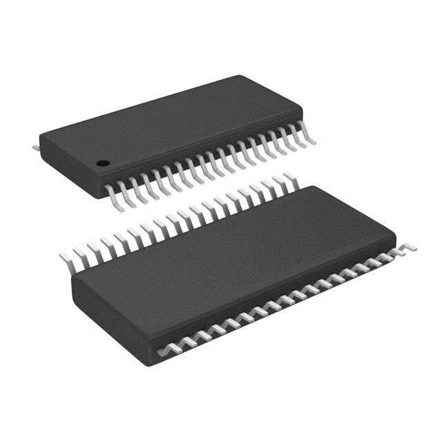
| 描述 | IC DUAL 8-BIT MLTPLY DAC 20-SOIC数模转换器- DAC 8bit .1us 5-15V |
| 产品分类 | |
| 品牌 | Texas Instruments |
| 产品手册 | |
| 产品图片 |
|
| rohs | 符合RoHS无铅 / 符合限制有害物质指令(RoHS)规范要求 |
| 产品系列 | 数据转换器IC,数模转换器- DAC,Texas Instruments TLC7528CDWR- |
| 数据手册 | |
| 产品型号 | TLC7528CDWR |
| 产品培训模块 | http://www.digikey.cn/PTM/IndividualPTM.page?site=cn&lang=zhs&ptm=13240 |
| 产品目录页面 | |
| 产品种类 | 数模转换器- DAC |
| 位数 | 8 |
| 供应商器件封装 | 20-SOIC |
| 其它名称 | 296-1340-6 |
| 分辨率 | 8 bit |
| 制造商产品页 | http://www.ti.com/general/docs/suppproductinfo.tsp?distId=10&orderablePartNumber=TLC7528CDWR |
| 包装 | Digi-Reel® |
| 单位重量 | 537.300 mg |
| 商标 | Texas Instruments |
| 安装类型 | 表面贴装 |
| 安装风格 | SMD/SMT |
| 封装 | Reel |
| 封装/外壳 | 20-SOIC(0.295",7.50mm 宽) |
| 封装/箱体 | SOIC-20 |
| 工作温度 | 0°C ~ 70°C |
| 工厂包装数量 | 2000 |
| 建立时间 | 100ns |
| 接口类型 | Parallel |
| 数据接口 | 并联 |
| 最大工作温度 | + 70 C |
| 最小工作温度 | 0 C |
| 标准包装 | 1 |
| 电压参考 | External |
| 电压源 | 单电源 |
| 电源电压-最大 | 5.25 V, 15.5 V |
| 电源电压-最小 | 4.75 V, 14.5 V |
| 积分非线性 | +/- 0.5 LSB |
| 稳定时间 | 100 ns |
| 系列 | TLC7528 |
| 结构 | R-2R |
| 转换器数 | 2 |
| 转换器数量 | 2 |
| 输出数和类型 | 2 电流,双极 |
| 输出类型 | Current |
| 采样比 | 10 MSPs |
| 采样率(每秒) | - |


- 商务部:美国ITC正式对集成电路等产品启动337调查
- 曝三星4nm工艺存在良率问题 高通将骁龙8 Gen1或转产台积电
- 太阳诱电将投资9.5亿元在常州建新厂生产MLCC 预计2023年完工
- 英特尔发布欧洲新工厂建设计划 深化IDM 2.0 战略
- 台积电先进制程称霸业界 有大客户加持明年业绩稳了
- 达到5530亿美元!SIA预计今年全球半导体销售额将创下新高
- 英特尔拟将自动驾驶子公司Mobileye上市 估值或超500亿美元
- 三星加码芯片和SET,合并消费电子和移动部门,撤换高东真等 CEO
- 三星电子宣布重大人事变动 还合并消费电子和移动部门
- 海关总署:前11个月进口集成电路产品价值2.52万亿元 增长14.8%


PDF Datasheet 数据手册内容提取
(cid:1)(cid:2)(cid:3)(cid:4)(cid:5)(cid:6)(cid:7)(cid:3)(cid:8) (cid:1)(cid:2)(cid:3)(cid:4)(cid:5)(cid:6)(cid:7)(cid:9)(cid:8) (cid:1)(cid:2)(cid:3)(cid:4)(cid:5)(cid:6)(cid:7)(cid:10) (cid:11)(cid:12)(cid:13)(cid:2) (cid:7)(cid:14)(cid:15)(cid:10)(cid:1) (cid:16)(cid:12)(cid:2)(cid:1)(cid:10)(cid:17)(cid:2)(cid:18)(cid:10)(cid:19)(cid:20) (cid:11)(cid:10)(cid:20)(cid:10)(cid:1)(cid:13)(cid:2)(cid:14)(cid:1)(cid:21)(cid:14)(cid:13)(cid:19)(cid:13)(cid:2)(cid:21)(cid:20) (cid:3)(cid:21)(cid:19)(cid:22)(cid:9)(cid:23)(cid:1)(cid:9)(cid:23)(cid:24) SLAS062E − JANUARY 1987 − REVISED NOVEMBER 2008 (cid:1) Easily Interfaced to Microprocessors DW, N OR PW PACKAGE (cid:1) (TOP VIEW) On-Chip Data Latches (cid:1) Monotonic Over the Entire A/D Conversion AGND 1 20 OUTB Range OUTA 2 19 RFBB (cid:1) Interchangeable With Analog Devices RFBA 3 18 REFB AD7528 and PMI PM-7528 REFA 4 17 VDD (cid:1) Fast Control Signaling for Digital Signal DGND 5 16 WR Processor (DSP) Applications Including DACA/DACB 6 15 CS Interface With TMS320 (MSB) DB7 7 14 DB0 (LSB) (cid:1) Voltage-Mode Operation DB6 8 13 DB1 (cid:1) DB5 9 12 DB2 CMOS Technology DB4 10 11 DB3 KEY PERFORMANCE SPECIFICATIONS Resolution 8 bits FN PACKAGE Linearity Error 1/2LSB (TOP VIEW) Power Dissipation at VDD = 5V 20mW A A DB B Settling Time at VDD = 5V 100ns FB UT GNUT FB Propagation Delay Time at VDD = 5V 80ns R O AO R 3 2 1 20 19 description REFA 4 18 REFB DGND 5 17 VDD The TLC7528C, TLC7528E, and TLC7528I are DACA/DACB 6 16 WR dual, 8-bit, digital-to-analog converters (DACs) (MSB) DB7 7 15 CS designed with separate on-chip data latches and DB6 8 14 DB0 (LSB) feature exceptionally close DAC-to-DAC match- 9 10 11 12 13 ing. Data are transferred to either of the two DAC data latches through a common, 8-bit, input port. B5 B4 B3B2 B1 D D DD D Control input DACA/DACB determines which DAC is to be loaded. The load cycle of these devices is similar to the write cycle of a random-access memory, allowing easy interface to most popular microprocessor buses and output ports. Segmenting the high-order bits minimizes glitches during changes in the most significant bits, where glitch impulse is typically the strongest. These devices operate from a 5V to 15V power supply and dissipates less than 15mW (typical). The 2- or 4-quadrant multiplying makes these devices a sound choice for many microprocessor-controlled gain-setting and signal-control applications. It can be operated in voltage mode, which produces a voltage output rather than a current output. Refer to the typical application information in this data sheet. The TLC7528C is characterized for operation from 0°C to +70°C. The TLC7528I is characterized for operation from −25°C to +85°C. The TLC7528E is characterized for operation from −40°C to +85°C. Please be aware that an important notice concerning availability, standard warranty, and use in critical applications of TexasInstruments semiconductor products and disclaimers thereto appears at the end of this data sheet. All trademarks are the property of their respective owners. (cid:17)(cid:23)(cid:21)(cid:11)(cid:12)(cid:3)(cid:1)(cid:10)(cid:21)(cid:19) (cid:11)(cid:13)(cid:1)(cid:13) (cid:25)(cid:26)(cid:27)(cid:28)(cid:29)(cid:30)(cid:31)!(cid:25)(cid:28)(cid:26) (cid:25)" #$(cid:29)(cid:29)%(cid:26)! (cid:31)" (cid:28)(cid:27) &$’((cid:25)#(cid:31)!(cid:25)(cid:28)(cid:26) )(cid:31)!%* Copyright 2000−2008, Texas Instruments Incorporated (cid:17)(cid:29)(cid:28))$#!" #(cid:28)(cid:26)(cid:27)(cid:28)(cid:29)(cid:30) !(cid:28) "&%#(cid:25)(cid:27)(cid:25)#(cid:31)!(cid:25)(cid:28)(cid:26)" &%(cid:29) !+% !%(cid:29)(cid:30)" (cid:28)(cid:27) (cid:1)%,(cid:31)" (cid:10)(cid:26)"!(cid:29)$(cid:30)%(cid:26)!" "!(cid:31)(cid:26))(cid:31)(cid:29)) -(cid:31)(cid:29)(cid:29)(cid:31)(cid:26)!.* (cid:17)(cid:29)(cid:28))$#!(cid:25)(cid:28)(cid:26) &(cid:29)(cid:28)#%""(cid:25)(cid:26)/ )(cid:28)%" (cid:26)(cid:28)! (cid:26)%#%""(cid:31)(cid:29)(cid:25)(. (cid:25)(cid:26)#($)% !%"!(cid:25)(cid:26)/ (cid:28)(cid:27) (cid:31)(( &(cid:31)(cid:29)(cid:31)(cid:30)%!%(cid:29)"* POST OFFICE BOX 655303 • DALLAS, TEXAS 75265 1
(cid:1)(cid:2)(cid:3)(cid:4)(cid:5)(cid:6)(cid:7)(cid:3)(cid:8) (cid:1)(cid:2)(cid:3)(cid:4)(cid:5)(cid:6)(cid:7)(cid:9)(cid:8) (cid:1)(cid:2)(cid:3)(cid:4)(cid:5)(cid:6)(cid:7)(cid:10) (cid:11)(cid:12)(cid:13)(cid:2) (cid:7)(cid:14)(cid:15)(cid:10)(cid:1) (cid:16)(cid:12)(cid:2)(cid:1)(cid:10)(cid:17)(cid:2)(cid:18)(cid:10)(cid:19)(cid:20) (cid:11)(cid:10)(cid:20)(cid:10)(cid:1)(cid:13)(cid:2)(cid:14)(cid:1)(cid:21)(cid:14)(cid:13)(cid:19)(cid:13)(cid:2)(cid:21)(cid:20) (cid:3)(cid:21)(cid:19)(cid:22)(cid:9)(cid:23)(cid:1)(cid:9)(cid:23)(cid:24) SLAS062E − JANUARY 1987 − REVISED NOVEMBER 2008 functional block diagram 14 DB0 REFA 13 3 RFBA 12 ÎÎÎ Î4ÎÎÎÎ 2 11 8 ÎÎÎ ÎÎÎÎÎ OUTA Input 8 Data Latch A DACA 10 Buffer ÎÎÎ ÎÎÎÎÎ Inputs 9 ÎÎÎ ÎÎÎÎÎ 8 1 AGND 7 DB7 19 RFBB ÎÎÎ ÎÎÎÎÎ 20 6 8 ÎÎÎ ÎÎÎÎÎ OUTB DACA/DACB 8 16 Logic ÎLaÎtch ÎB ÎÎDAÎCBÎÎ WR 15 Control CS ÎÎÎ ÎÎÎÎÎ 18 REFB operating sequence tsu(CS) th(CS) CS tsu(DAC) th(DAC) DACA/DACB tw(WR) WR tsu(D) th(D) DB0−DB7 Data In Stable 2 POST OFFICE BOX 655303 • DALLAS, TEXAS 75265
(cid:1)(cid:2)(cid:3)(cid:4)(cid:5)(cid:6)(cid:7)(cid:3)(cid:8) (cid:1)(cid:2)(cid:3)(cid:4)(cid:5)(cid:6)(cid:7)(cid:9)(cid:8) (cid:1)(cid:2)(cid:3)(cid:4)(cid:5)(cid:6)(cid:7)(cid:10) (cid:11)(cid:12)(cid:13)(cid:2) (cid:7)(cid:14)(cid:15)(cid:10)(cid:1) (cid:16)(cid:12)(cid:2)(cid:1)(cid:10)(cid:17)(cid:2)(cid:18)(cid:10)(cid:19)(cid:20) (cid:11)(cid:10)(cid:20)(cid:10)(cid:1)(cid:13)(cid:2)(cid:14)(cid:1)(cid:21)(cid:14)(cid:13)(cid:19)(cid:13)(cid:2)(cid:21)(cid:20) (cid:3)(cid:21)(cid:19)(cid:22)(cid:9)(cid:23)(cid:1)(cid:9)(cid:23)(cid:24) SLAS062E − JANUARY 1987 − REVISED NOVEMBER 2008 absolute maximum ratings over operating free-air temperature range (unless otherwise noted)† Supply voltage range, V (to AGND or DGND) . . . . . . . . . . . . . . . . . . . . . . . . . . . . . . . . . . . . . . −0.3V to 16.5V DD Voltage between AGND and DGND . . . . . . . . . . . . . . . . . . . . . . . . . . . . . . . . . . . . . . . . . . . . . . . . . . . . . . . . . ±V DD Input voltage range, V (to DGND) . . . . . . . . . . . . . . . . . . . . . . . . . . . . . . . . . . . . . . . . . . . . . . . −0.3V to V + 0.3 I DD Reference voltage, V or V (to AGND) . . . . . . . . . . . . . . . . . . . . . . . . . . . . . . . . . . . . . . . . . . . . . . . . . ±25V refA refB Feedback voltage V or V (to AGND) . . . . . . . . . . . . . . . . . . . . . . . . . . . . . . . . . . . . . . . . . . . . . . . ±25V RFBA RFBB Input voltage (voltage mode out A, out B to AGND) . . . . . . . . . . . . . . . . . . . . . . . . . . . . . . . . −0.3V to V + 0.3 DD Output voltage, V or V (to AGND) . . . . . . . . . . . . . . . . . . . . . . . . . . . . . . . . . . . . . . . . . . . . . . . . . . . . . . ±25V OA OB Peak input current . . . . . . . . . . . . . . . . . . . . . . . . . . . . . . . . . . . . . . . . . . . . . . . . . . . . . . . . . . . . . . . . . . . . . . . . 10µA Operating free-air temperature range, T : TLC7528C . . . . . . . . . . . . . . . . . . . . . . . . . . . . . . . . . . 0°C to +70°C A TLC7528I . . . . . . . . . . . . . . . . . . . . . . . . . . . . . . . −25°C to +85°C TLC7528E . . . . . . . . . . . . . . . . . . . . . . . . . . . . . . . −40°C to +85°C Storage temperature range, T . . . . . . . . . . . . . . . . . . . . . . . . . . . . . . . . . . . . . . . . . . . . . . . . . −65°C to +150°C stg Case temperature for 10 seconds, T : FN package . . . . . . . . . . . . . . . . . . . . . . . . . . . . . . . . . . . . . . . . . +260°C C Lead temperature 1,6mm (1/16 inch) from case for 10 seconds: DW or N package . . . . . . . . . . . . . . +260°C †Stresses beyond those listed under “absolute maximum ratings” may cause permanent damage to the device. These are stress ratings only, and functional operation of the device at these or any other conditions beyond those indicated under “recommended operating conditions” is not implied. Exposure to absolute-maximum-rated conditions for extended periods may affect device reliability. package/ordering information For the most current package and ordering information, see the Package Option Addendum at the end of this document, or see the TI website at www.ti.com. recommended operating conditions VDD = 4.75V to 5.25V VDD = 14.5V to 15.5V UUNNIITT MIN NOM MAX MIN NOM MAX Reference voltage, VrefA or VrefB ±10 ±10 V High-level input voltage, VIH 2.4 13.5 V Low-level input voltage, VIL 0.8 1.5 V CS setup time, tsu(CS) 50 50 ns CS hold time, th(CS) 0 0 ns DAC select setup time, tsu(DAC) 50 50 ns DAC select hold time, th(DAC) 10 10 ns Data bus input setup time tsu(D) 25 25 ns Data bus input hold time th(D) 10 10 ns Pulse duration, WR low, tw(WR) 50 50 ns TLC7628C 0 +70 0 +70 OOppeerraattiinngg ffrreeee--aaiirr tteemmppeerraattuurree,, TTAA TLC7628I −25 +85 −25 +85 °CC TLC7628E −40 +85 −40 +85 POST OFFICE BOX 655303 • DALLAS, TEXAS 75265 3
(cid:1)(cid:2)(cid:3)(cid:4)(cid:5)(cid:6)(cid:7)(cid:3)(cid:8) (cid:1)(cid:2)(cid:3)(cid:4)(cid:5)(cid:6)(cid:7)(cid:9)(cid:8) (cid:1)(cid:2)(cid:3)(cid:4)(cid:5)(cid:6)(cid:7)(cid:10) (cid:11)(cid:12)(cid:13)(cid:2) (cid:7)(cid:14)(cid:15)(cid:10)(cid:1) (cid:16)(cid:12)(cid:2)(cid:1)(cid:10)(cid:17)(cid:2)(cid:18)(cid:10)(cid:19)(cid:20) (cid:11)(cid:10)(cid:20)(cid:10)(cid:1)(cid:13)(cid:2)(cid:14)(cid:1)(cid:21)(cid:14)(cid:13)(cid:19)(cid:13)(cid:2)(cid:21)(cid:20) (cid:3)(cid:21)(cid:19)(cid:22)(cid:9)(cid:23)(cid:1)(cid:9)(cid:23)(cid:24) SLAS062E − JANUARY 1987 − REVISED NOVEMBER 2008 electrical characteristics over recommended operating free-air temperature range, V = V = 10V, V and V at 0V (unless otherwise noted) refA refB OA OB VDD = 5V VDD = 15V PPAARRAAMMEETTEERR TTEESSTT CCOONNDDIITTIIOONNSS UUNNIITT MIN TYP† MAX MIN TYP† MAX IIH High-level input current VI = VDD 10 10 µA IIL Low-level input current VI = 0 5 12 −10 5 12 −10 µA Reference input impedance 20 20 kΩ REFA or REFB to AGND DAC data latch loaded with OUTA ±400 ±200 00000000, VrefA = ±10V IIIIkkgg OOuuttppuutt lleeaakkaaggee ccuurrrreenntt nnAA DAC data latch loaded with OUTB ±400 ±200 00000000, VrefB = ±10V Input resistance match ±1% ±1% (REFA to REFB) DC supply sensitivity, ∆gain/∆VDD ∆VDD = ±10% 0.04 0.02 %/% All digital inputs at VIHmin or IDD Supply current (quiescent) VILmax 2 2 mA IDD Supply current (standby) All digital inputs at 0V or VDD 0.5 0.5 mA DB0−DB7 10 10 pF Ci Input capacitance WR, CS, 15 15 pF DACA/DACB DAC data latches loaded with 50 50 00000000 CCoo OOuuttppuutt ccaappaacciittaannccee ((OOUUTTAA,, OOUUTTBB)) ppFF DAC data latches loaded with 120 120 11111111 †All typical values are at TA = +25°C. 4 POST OFFICE BOX 655303 • DALLAS, TEXAS 75265
(cid:1)(cid:2)(cid:3)(cid:4)(cid:5)(cid:6)(cid:7)(cid:3)(cid:8) (cid:1)(cid:2)(cid:3)(cid:4)(cid:5)(cid:6)(cid:7)(cid:9)(cid:8) (cid:1)(cid:2)(cid:3)(cid:4)(cid:5)(cid:6)(cid:7)(cid:10) (cid:11)(cid:12)(cid:13)(cid:2) (cid:7)(cid:14)(cid:15)(cid:10)(cid:1) (cid:16)(cid:12)(cid:2)(cid:1)(cid:10)(cid:17)(cid:2)(cid:18)(cid:10)(cid:19)(cid:20) (cid:11)(cid:10)(cid:20)(cid:10)(cid:1)(cid:13)(cid:2)(cid:14)(cid:1)(cid:21)(cid:14)(cid:13)(cid:19)(cid:13)(cid:2)(cid:21)(cid:20) (cid:3)(cid:21)(cid:19)(cid:22)(cid:9)(cid:23)(cid:1)(cid:9)(cid:23)(cid:24) SLAS062E − JANUARY 1987 − REVISED NOVEMBER 2008 operating characteristics over recommended operating free-air temperature range, V = V = 10V, V and V at 0V (unless otherwise noted) refA refB OA OB VDD = 5V VDD = 15V PPAARRAAMMEETTEERR TTEESSTT CCOONNDDIITTIIOONNSS UUNNIITT MIN TYP MAX MIN TYP MAX Linearity error ±1/2 ±1/2 LSB Settling time (to 1/2LSB) See Note 1 100 100 ns Gain error See Note 2 2.5 2.5 LSB REFA to OUTA −65 −65 AACC ffeeeeddtthhrroouugghh SSeeee NNoottee 33 ddBB REFB to OUTB −65 −65 Temperature coefficient of gain See Note 4 0.007 0.0035 %FSR/°C Propagation delay (from digital input to See Note 5 80 80 ns 90% of final analog output current) CChhaannnneell--ttoo--cchhaannnneell REFA to OUTB See Note 6 77 77 ddBB isolation REFB to OUTA See Note 7 77 77 Measured for code transition from Digital-to-analog glitch impulse area 00000000 to 11111111, 160 440 nV−s TA = +25°C Measured for code transition from Digital crosstalk 00000000 to 11111111, 30 60 nV−s TA = +25°C Harmonic distortion Vi = 6V, f = 1kHz, TA = +25°C −85 −85 dB NOTES: 1. OUTA, OUTB load = 100Ω, Cext = 13pF; WR and CS at 0V; DB0−DB7 at 0V to VDD or VDD to 0V. 2. Gain error is measured using an internal feedback resistor. Nominal full scale range (FSR) = Vref − 1LSB. 3. Vref = 20V peak-to-peak, 100kHz sine wave; DAC data latches loaded with 00000000. 4. Temperature coefficient of gain measured from 0°C to +25°C or from +25°C to +70°C. 5. VrefA = VrefB = 10V; OUTA/OUTB load = 100Ω, Cext = 13pF; WR and CS at 0V; DB0−DB7 at 0V to VDD or VDD to 0V. 6. Both DAC latches loaded with 11111111; VrefA = 20V peak-to-peak, 100kHz sine wave; VrefB = 0; TA = +25°C. 7. Both DAC latches loaded with 11111111; VrefB = 20V peak-to-peak, 100kHz sine wave; VrefA = 0; TA = +25°C. PRINCIPLES OF OPERATION These devices contain two identical, 8-bit-multiplying DACs, DACA and DACB. Each DAC consists of an inverted R-2R ladder, analog switches, and input data latches. Binary-weighted currents are switched between DAC output and AGND, thus maintaining a constant current in each ladder leg independent of the switch state. Most applications require only the addition of an external operational amplifier and voltage reference. A simplified DAC circuit for DACA with all digital inputs low is shown in Figure 1. Figure 2 shows the DACA equivalent circuit. A similar equivalent circuit can be drawn for DACB. Both DACs share the analog ground terminal 1 (AGND). With all digital inputs high, the entire reference current flows to OUTA. A small leakage current (I ) flows across internal junctions, and as with most semiconductor devices, Ikg doubles every 10°C. C is due to the parallel combination of the NMOS switches and has a value that depends o on the number of switches connected to the output. The range of C is 50pF to 120pF maximum. The equivalent o output resistance (r ) varies with the input code from 0.8R to 3R where R is the nominal value of the ladder o resistor in the R-2R network. These devices interface to a microprocessor through the data bus, CS, WR, and DACA/DACB control signals. When CS and WR are both low, the TLC7528 analog output, specified by the DACA/DACB control line, responds to the activity on the DB0−DB7 data bus inputs. In this mode, the input latches are transparent and input data directly affects the analog output. When either the CS signal or WR signal goes high, the data on the DB0−DB7 inputs are latched until the CS and WR signals go low again. When CS is high, the data inputs are disabled regardless of the state of the WR signal. POST OFFICE BOX 655303 • DALLAS, TEXAS 75265 5
(cid:1)(cid:2)(cid:3)(cid:4)(cid:5)(cid:6)(cid:7)(cid:3)(cid:8) (cid:1)(cid:2)(cid:3)(cid:4)(cid:5)(cid:6)(cid:7)(cid:9)(cid:8) (cid:1)(cid:2)(cid:3)(cid:4)(cid:5)(cid:6)(cid:7)(cid:10) (cid:11)(cid:12)(cid:13)(cid:2) (cid:7)(cid:14)(cid:15)(cid:10)(cid:1) (cid:16)(cid:12)(cid:2)(cid:1)(cid:10)(cid:17)(cid:2)(cid:18)(cid:10)(cid:19)(cid:20) (cid:11)(cid:10)(cid:20)(cid:10)(cid:1)(cid:13)(cid:2)(cid:14)(cid:1)(cid:21)(cid:14)(cid:13)(cid:19)(cid:13)(cid:2)(cid:21)(cid:20) (cid:3)(cid:21)(cid:19)(cid:22)(cid:9)(cid:23)(cid:1)(cid:9)(cid:23)(cid:24) SLAS062E − JANUARY 1987 − REVISED NOVEMBER 2008 PRINCIPLES OF OPERATION The digital inputs of these devices provide TTL compatibility when operated from a supply voltage of 5V. These devices can operate with any supply voltage in the range from 5V to 15V; however, input logic levels are not TTL-compatible above 5V. R R R REFA 2R 2R 2R 2R 2R RFB RFBA S1 S2 S3 S8 OUTA AGND DACA Data Latches and Drivers Figure 1. Simplified Functional Circuit for DACA RFBA RFB R REFA OUTA I 256 IIkg COUT AGND Figure 2. TLC7528 Equivalent Circuit, DACA Latch Loaded With 11111111 MODE SELECTION TABLE DACA/DACB CS WR DACA DACB L L L Write Hold H L L Hold Write X H X Hold Hold X X H Hold Hold L = low level, H = high level, X = don’t care 6 POST OFFICE BOX 655303 • DALLAS, TEXAS 75265
(cid:1)(cid:2)(cid:3)(cid:4)(cid:5)(cid:6)(cid:7)(cid:3)(cid:8) (cid:1)(cid:2)(cid:3)(cid:4)(cid:5)(cid:6)(cid:7)(cid:9)(cid:8) (cid:1)(cid:2)(cid:3)(cid:4)(cid:5)(cid:6)(cid:7)(cid:10) (cid:11)(cid:12)(cid:13)(cid:2) (cid:7)(cid:14)(cid:15)(cid:10)(cid:1) (cid:16)(cid:12)(cid:2)(cid:1)(cid:10)(cid:17)(cid:2)(cid:18)(cid:10)(cid:19)(cid:20) (cid:11)(cid:10)(cid:20)(cid:10)(cid:1)(cid:13)(cid:2)(cid:14)(cid:1)(cid:21)(cid:14)(cid:13)(cid:19)(cid:13)(cid:2)(cid:21)(cid:20) (cid:3)(cid:21)(cid:19)(cid:22)(cid:9)(cid:23)(cid:1)(cid:9)(cid:23)(cid:24) SLAS062E − JANUARY 1987 − REVISED NOVEMBER 2008 APPLICATION INFORMATION These devices are capable of performing 2-quadrant or full 4-quadrant multiplication. Circuit configurations for 2-quadrant and 4-quadrant multiplication are shown in Figure 3 and Figure 4. Table 1 and Table 2 summarize input coding for unipolar and bipolar operation, respectively. VI(A) ±10 V R1 (see Note A) R2 (see Note A) RFBA C1 17 VDD REFA (see Note B) 14 DB0 ÎÎÎÎOUTA Input 8 − Buffer Latch 8 ÎÎDACÎA Î VOA DB7 + ÎÎÎÎ 7 AGND R4 (see Note A) RFBB C2 ÎÎÎ ÎÎÎÎ (see Note B) OUTB 6 8 ÎÎÎ ÎÎÎÎ DACA/DACCSB 15 CLoongtricol ÎLÎatchÎ8 ÎÎDACÎB Î − VOB 16 + WR ÎÎÎ ÎÎÎÎAGND 5 REFB AGND DGND RECOMMENDED TRIM R3 (see Note A) RESISTOR VALUES R1, R3 500 Ω VI(B) R2, R4 150 Ω ±10 V NOTES: A. R1, R2, R3, and R4 are used only if gain adjustment is required. See table for recommended values. Make gain adjustment with digital input of 255. B. C1 and C2 phase compensation capacitors (10pF to 15pF) are required when using high-speed amplifiers to prevent ringing or oscillation. Figure 3. Unipolar Operation (2-Quadrant Multiplication) POST OFFICE BOX 655303 • DALLAS, TEXAS 75265 7
(cid:1)(cid:2)(cid:3)(cid:4)(cid:5)(cid:6)(cid:7)(cid:3)(cid:8) (cid:1)(cid:2)(cid:3)(cid:4)(cid:5)(cid:6)(cid:7)(cid:9)(cid:8) (cid:1)(cid:2)(cid:3)(cid:4)(cid:5)(cid:6)(cid:7)(cid:10) (cid:11)(cid:12)(cid:13)(cid:2) (cid:7)(cid:14)(cid:15)(cid:10)(cid:1) (cid:16)(cid:12)(cid:2)(cid:1)(cid:10)(cid:17)(cid:2)(cid:18)(cid:10)(cid:19)(cid:20) (cid:11)(cid:10)(cid:20)(cid:10)(cid:1)(cid:13)(cid:2)(cid:14)(cid:1)(cid:21)(cid:14)(cid:13)(cid:19)(cid:13)(cid:2)(cid:21)(cid:20) (cid:3)(cid:21)(cid:19)(cid:22)(cid:9)(cid:23)(cid:1)(cid:9)(cid:23)(cid:24) SLAS062E − JANUARY 1987 − REVISED NOVEMBER 2008 APPLICATION INFORMATION VI(A) R6 ±10 V 20 kΩ (see Note B) R1 (see Note A) RFBA R2 (see Note A) C1 VDD 17 ÎÎÎÎ (see Note C) R5 DB0 14 ÎIÎnpuÎt Î 8 ÎÎÎ8 OUTA − 10R k7Ω 20 kΩ ÎBÎuffeÎr Î ÎLaÎtchÎ DACA AGND A1 − DB7 7 ÎÎÎÎ + (see Note B) +A2 VOA R11 DACA/ 6 ÎÎÎÎ RFBB R4 (see Note A) 5 kΩ DACB 15 ÎÎCoÎntroÎl C2 R8 CS Logic (see Note C) 20 kΩ WR 16 ÎÎÎÎ 8 ÎÎÎ8 OUTB − 5 ÎLaÎtchÎ DACB A3 − AGND + R9 A4 VOB REFB 10 kΩ + DGND AGND (see Note B) R11 5 kΩ R3 AGND (see Note A) R10 VI(B) 20 kΩ ±10 V (see Note B) NOTES: A. R1, R2, R3, and R4 are used only if gain adjustment is required. See table in Figure 3 for recommended values. Adjust R1 for VOA = 0V with code 10000000 in DACA latch. Adjust R3 for VOB = 0V with 10000000 in DACB latch. B. Matching and tracking are essential for resistor pairs R6, R7, R9, and R10. C. C1 and C2 phase compensation capacitors (10pF to 15pF) may be required if A1 and A3 are high-speed amplifiers. Figure 4. Bipolar Operation (4-Quadrant Operation) Table 1. Unipolar Binary Code Table 2. Bipolar (Offset Binary) Code DAC LATCH CONTENTS DAC LATCH CONTENTS AANNAALLOOGG OOUUTTPPUUTT AANNAALLOOGG OOUUTTPPUUTT MSB LSB† MSB LSB‡ 1 1 1 1 1 1 1 1 −VI (255/256) 1 1 1 1 1 1 1 1 VI (127/128) 1 0 0 0 0 0 0 1 −VI (129/256) 1 0 0 0 0 0 0 1 VI (1/128) 1 0 0 0 0 0 0 0 −VI (128/256) = −Vi/2 1 0 0 0 0 0 0 0 0V 0 1 1 1 1 1 1 1 −VI (127/256) 0 1 1 1 1 1 1 1 −VI (1/128) 0 0 0 0 0 0 0 1 −VI (1/256) 0 0 0 0 0 0 0 1 −VI (127/128) 0 0 0 0 0 0 0 0 −VI (0/256) = 0 0 0 0 0 0 0 0 0 −VI (128/128) †1LSB = (2−8)VI ‡1LSB = (2−7)VI 8 POST OFFICE BOX 655303 • DALLAS, TEXAS 75265
(cid:1)(cid:2)(cid:3)(cid:4)(cid:5)(cid:6)(cid:7)(cid:3)(cid:8) (cid:1)(cid:2)(cid:3)(cid:4)(cid:5)(cid:6)(cid:7)(cid:9)(cid:8) (cid:1)(cid:2)(cid:3)(cid:4)(cid:5)(cid:6)(cid:7)(cid:10) (cid:11)(cid:12)(cid:13)(cid:2) (cid:7)(cid:14)(cid:15)(cid:10)(cid:1) (cid:16)(cid:12)(cid:2)(cid:1)(cid:10)(cid:17)(cid:2)(cid:18)(cid:10)(cid:19)(cid:20) (cid:11)(cid:10)(cid:20)(cid:10)(cid:1)(cid:13)(cid:2)(cid:14)(cid:1)(cid:21)(cid:14)(cid:13)(cid:19)(cid:13)(cid:2)(cid:21)(cid:20) (cid:3)(cid:21)(cid:19)(cid:22)(cid:9)(cid:23)(cid:1)(cid:9)(cid:23)(cid:24) SLAS062E − JANUARY 1987 − REVISED NOVEMBER 2008 APPLICATION INFORMATION microprocessor interface information 8 A8−A15 Address Bus DACA/DACB A Address Decode CS CPU Logic A + 1 TLC7528 WR 8051 DB0 WR DB7 ALE Latch 8 Data Bus AD0−AD7 NOTE A: A = decoded address for TLC7528 DACA A + 1 = decoded address for TLC7528 DACB Figure 5. TLC7528: Intel 8051 Interface 8 A8−A15 Address Bus DACA/DACB A Address VMA Decode CS Logic A + 1 TLC7528 CPU WR 6800 DB0 φ2 DB7 8 AD0−AD7 Data Bus NOTE A: A = decoded address for TLC7528 DACA A + 1 = decoded address for TLC7528 DACB Figure 6. TLC7528: 6800 Interface POST OFFICE BOX 655303 • DALLAS, TEXAS 75265 9
(cid:1)(cid:2)(cid:3)(cid:4)(cid:5)(cid:6)(cid:7)(cid:3)(cid:8) (cid:1)(cid:2)(cid:3)(cid:4)(cid:5)(cid:6)(cid:7)(cid:9)(cid:8) (cid:1)(cid:2)(cid:3)(cid:4)(cid:5)(cid:6)(cid:7)(cid:10) (cid:11)(cid:12)(cid:13)(cid:2) (cid:7)(cid:14)(cid:15)(cid:10)(cid:1) (cid:16)(cid:12)(cid:2)(cid:1)(cid:10)(cid:17)(cid:2)(cid:18)(cid:10)(cid:19)(cid:20) (cid:11)(cid:10)(cid:20)(cid:10)(cid:1)(cid:13)(cid:2)(cid:14)(cid:1)(cid:21)(cid:14)(cid:13)(cid:19)(cid:13)(cid:2)(cid:21)(cid:20) (cid:3)(cid:21)(cid:19)(cid:22)(cid:9)(cid:23)(cid:1)(cid:9)(cid:23)(cid:24) SLAS062E − JANUARY 1987 − REVISED NOVEMBER 2008 APPLICATION INFORMATION 8 A8−A15 Address Bus DACA/DACB A Address IORQ Decode CS Logic A + 1 TLC7528 CPU WR Z80-A DB0 WR DB7 8 Data Bus D0−D7 NOTE A: A = decoded address for TLC7528 DACA A + 1 = decoded address for TLC7528 DACB Figure 7. TLC7528 To Z-80A Interface programmable window detector The programmable window comparator shown in Figure 8 determines if the voltage applied to the DAC feedback resistors is within the limits programmed into the data latches of these devices. Input signal range depends on the reference and polarity; that is, the test input range is 0 to −V . The DACA and DACB data ref latches are programmed with the upper and lower test limits. A signal within the programmed limits drives the output high. 10 POST OFFICE BOX 655303 • DALLAS, TEXAS 75265
(cid:1)(cid:2)(cid:3)(cid:4)(cid:5)(cid:6)(cid:7)(cid:3)(cid:8) (cid:1)(cid:2)(cid:3)(cid:4)(cid:5)(cid:6)(cid:7)(cid:9)(cid:8) (cid:1)(cid:2)(cid:3)(cid:4)(cid:5)(cid:6)(cid:7)(cid:10) (cid:11)(cid:12)(cid:13)(cid:2) (cid:7)(cid:14)(cid:15)(cid:10)(cid:1) (cid:16)(cid:12)(cid:2)(cid:1)(cid:10)(cid:17)(cid:2)(cid:18)(cid:10)(cid:19)(cid:20) (cid:11)(cid:10)(cid:20)(cid:10)(cid:1)(cid:13)(cid:2)(cid:14)(cid:1)(cid:21)(cid:14)(cid:13)(cid:19)(cid:13)(cid:2)(cid:21)(cid:20) (cid:3)(cid:21)(cid:19)(cid:22)(cid:9)(cid:23)(cid:1)(cid:9)(cid:23)(cid:24) SLAS062E − JANUARY 1987 − REVISED NOVEMBER 2008 APPLICATION INFORMATION VDD VCC Test Input 0 to −Vref 3 17 RFBA 1 kΩ OUTA 2 4 − DACA REFA + 8 14−7 Data Inputs DB0−DB7 TLC7528 1 15 PASS/FAIL Output CS AGND 16 WR 6 DACA/DACB OUTB 20 18 REFB − Vref DACB 5 + DGND RFBB 19 Figure 8. Digitally-Programmable Window Comparator (Upper- and Lower-Limit Tester) digitally-controlled signal attenuator Figure 9 shows a TLC7528 configured as a two-channel programmable attenuator. Applications include stereo audio and telephone signal level control. Table 3 shows input codes vs attenuation for a 0dB to 15.5dB range. Attenuation dB = −20 log10 D/256, D = digital input code 17 RFBA 3 VDD OUTA 2 VIA 4 REFA DACA A1 Output 14−7 8 DB0−DB7 Data Bus TLC7528 15 CS 16 WR 6 DACA/DACB 20 OUTB REFB 18 DACB VOB A2 1 AGND 5 DGND RFBB 19 Figure 9. Digitally Controlled Dual Telephone Attenuator POST OFFICE BOX 655303 • DALLAS, TEXAS 75265 11
(cid:1)(cid:2)(cid:3)(cid:4)(cid:5)(cid:6)(cid:7)(cid:3)(cid:8) (cid:1)(cid:2)(cid:3)(cid:4)(cid:5)(cid:6)(cid:7)(cid:9)(cid:8) (cid:1)(cid:2)(cid:3)(cid:4)(cid:5)(cid:6)(cid:7)(cid:10) (cid:11)(cid:12)(cid:13)(cid:2) (cid:7)(cid:14)(cid:15)(cid:10)(cid:1) (cid:16)(cid:12)(cid:2)(cid:1)(cid:10)(cid:17)(cid:2)(cid:18)(cid:10)(cid:19)(cid:20) (cid:11)(cid:10)(cid:20)(cid:10)(cid:1)(cid:13)(cid:2)(cid:14)(cid:1)(cid:21)(cid:14)(cid:13)(cid:19)(cid:13)(cid:2)(cid:21)(cid:20) (cid:3)(cid:21)(cid:19)(cid:22)(cid:9)(cid:23)(cid:1)(cid:9)(cid:23)(cid:24) SLAS062E − JANUARY 1987 − REVISED NOVEMBER 2008 APPLICATION INFORMATION Table 3. Attenuation vs DACA, DACB Code CODE IN CODE IN ATTEN (dB) DAC INPUT CODE ATTN (dB) DAC INPUT CODE DECIMAL DECIMAL 0 1 1 1 1 1 1 1 1 255 8.0 0 1 1 0 0 1 1 0 102 0.5 1 1 1 1 0 0 1 0 242 8.5 0 1 1 0 0 0 0 0 96 1.0 1 1 1 0 0 1 0 0 228 9.0 0 1 0 1 1 0 1 1 91 1.5 1 1 0 1 0 1 1 1 215 9.5 0 1 0 1 0 1 1 0 86 2.0 1 1 0 0 1 0 1 1 203 10.0 0 1 0 1 0 0 0 1 81 2.5 1 1 0 0 0 0 0 0 192 10.5 0 1 0 0 1 1 0 0 76 3.0 1 0 1 1 0 1 0 1 181 11.0 0 1 0 0 1 0 0 0 72 3.5 1 0 1 0 1 0 1 1 171 11.5 0 1 0 0 0 1 0 0 68 4.0 1 0 1 0 0 0 1 0 162 12.0 0 1 0 0 0 0 0 0 64 4.5 1 0 0 1 1 0 0 0 152 12.5 0 0 1 1 1 1 0 1 61 5.0 1 0 0 1 1 1 1 1 144 13.0 0 0 1 1 1 0 0 1 57 5.5 1 0 0 0 1 0 0 0 136 13.5 0 0 1 1 0 1 1 0 54 6.0 1 0 0 0 0 0 0 0 128 14.0 0 0 1 1 0 0 1 1 51 6.5 0 1 1 1 1 0 0 1 121 14.5 0 0 1 1 0 0 0 0 48 7.0 0 1 1 1 0 0 1 0 114 15.0 0 0 1 0 1 1 1 0 46 7.5 0 1 1 0 1 1 0 0 108 15.5 0 0 1 0 1 0 1 1 43 programmable state-variable filter This programmable state-variable or universal filter configuration provides low-pass, high-pass, and bandpass outputs, and is suitable for applications requiring microprocessor control of filter parameters. As shown in Figure 10, DACA1 and DACB1 control the gain and Q of the filter while DACA2 and DACB2 control the cutoff frequency. Both halves of the DACA2 and DACB2 must track accurately in order for the cutoff-frequency equation to be true. With the TLC7528, this validity is easy to achieve. f (cid:1) 1 c 2(cid:1)R1C1 The programmable range for the cutoff or center frequency is 0kHz to 15kHz with a Q ranging from 0.3 to 4.5. This parameter defines the limits of the component values. 12 POST OFFICE BOX 655303 • DALLAS, TEXAS 75265
(cid:1)(cid:2)(cid:3)(cid:4)(cid:5)(cid:6)(cid:7)(cid:3)(cid:8) (cid:1)(cid:2)(cid:3)(cid:4)(cid:5)(cid:6)(cid:7)(cid:9)(cid:8) (cid:1)(cid:2)(cid:3)(cid:4)(cid:5)(cid:6)(cid:7)(cid:10) (cid:11)(cid:12)(cid:13)(cid:2) (cid:7)(cid:14)(cid:15)(cid:10)(cid:1) (cid:16)(cid:12)(cid:2)(cid:1)(cid:10)(cid:17)(cid:2)(cid:18)(cid:10)(cid:19)(cid:20) (cid:11)(cid:10)(cid:20)(cid:10)(cid:1)(cid:13)(cid:2)(cid:14)(cid:1)(cid:21)(cid:14)(cid:13)(cid:19)(cid:13)(cid:2)(cid:21)(cid:20) (cid:3)(cid:21)(cid:19)(cid:22)(cid:9)(cid:23)(cid:1)(cid:9)(cid:23)(cid:24) SLAS062E − JANUARY 1987 − REVISED NOVEMBER 2008 APPLICATION INFORMATION C3 47pF 4 REFA OUTA 2 R5 VI DACA 17 VDD (RS) 3 A1 30kΩ 8 RFBA + R4 DataIn AGND 1 TLC7528 R3 30kΩ 15 CS OUTB 20 10kΩ A2 HighPass 16 DACB Out WR 19 + 5 (RF) RFBB DGND REFB 18 6 DACA/DACB BandpassOut DACA1ANDDACB1 C1 1000pF 4 REFA DACA OUTA 2 (R1) 17 VDD 3 A3 C2 RFBA 8 + DataIn AGND 1 TLC7528 1000pF 15 CS OUTB 20 16 DACB WR 19 (R2) RFBB A4 LowPassOut 5 DGND REFB 18 + 6 DACA/DACB DACA2andDACB2 CircuitEquations: C1=C2,R1=R2,R4=R5 R R 3 F Q= R R 4 fb(DACB1) Where: R istheinternalresistorconnectedbetweenOUTBandRFBB fb R G − F R S NOTES: A. Op-amps A1, A2, A3, and A4 are TL287. B. CS compensates for the op-amp gain-bandwidth limitations. 256(cid:2)(DACladderresistance) C. DAC equivalent resistance equals DACdigitalcode Figure 10. Digitally-Controlled State-Variable Filter POST OFFICE BOX 655303 • DALLAS, TEXAS 75265 13
(cid:1)(cid:2)(cid:3)(cid:4)(cid:5)(cid:6)(cid:7)(cid:3)(cid:8) (cid:1)(cid:2)(cid:3)(cid:4)(cid:5)(cid:6)(cid:7)(cid:9)(cid:8) (cid:1)(cid:2)(cid:3)(cid:4)(cid:5)(cid:6)(cid:7)(cid:10) (cid:11)(cid:12)(cid:13)(cid:2) (cid:7)(cid:14)(cid:15)(cid:10)(cid:1) (cid:16)(cid:12)(cid:2)(cid:1)(cid:10)(cid:17)(cid:2)(cid:18)(cid:10)(cid:19)(cid:20) (cid:11)(cid:10)(cid:20)(cid:10)(cid:1)(cid:13)(cid:2)(cid:14)(cid:1)(cid:21)(cid:14)(cid:13)(cid:19)(cid:13)(cid:2)(cid:21)(cid:20) (cid:3)(cid:21)(cid:19)(cid:22)(cid:9)(cid:23)(cid:1)(cid:9)(cid:23)(cid:24) SLAS062E − JANUARY 1987 − REVISED NOVEMBER 2008 APPLICATION INFORMATION voltage-mode operation It is possible to operate the current multiplying D/A converter of these devices in a voltage mode. In the voltage mode, a fixed voltage is placed on the current output terminal. The analog output voltage is then available at the reference voltage terminal. Figure 11 is an example of a current multiplying D/A that operates in the voltage mode. R R R REF (Analog Output Voltage) 2R 2R 2R 2R R “0” “1” Out (Fixed Input Voltage) AGND Figure 11. Voltage-Mode Operation The following equation shows the relationship between the fixed input voltage and the analog output voltage: V = V (D/256) O I Where: V = analog output voltage O V = fixed input voltage (must not be forced below 0V.) I D = digital input code converted to decimal In voltage-mode operation, these devices meet the following specification: PARAMETER TEST CONDITIONS MIN MAX UNIT Linearity error at REFA or REFB VDD = 5V, OUTA or OUTB at 2.5V, TA = +25°C 1 LSB 14 POST OFFICE BOX 655303 • DALLAS, TEXAS 75265
Revision History DATE REV PAGE SECTION DESCRIPTION 11/08 E 13 Application Information Corrected Figure 10. Front Page — Deleted Available Options table. 66//0077 DD 3 — Inserted Package/Ordering information. NOTE: Page numbers for previous revisions may differ from page numbers in the current version.
PACKAGE OPTION ADDENDUM www.ti.com 6-Feb-2020 PACKAGING INFORMATION Orderable Device Status Package Type Package Pins Package Eco Plan Lead/Ball Finish MSL Peak Temp Op Temp (°C) Device Marking Samples (1) Drawing Qty (2) (6) (3) (4/5) TLC7528CDW ACTIVE SOIC DW 20 25 Green (RoHS NIPDAU Level-1-260C-UNLIM 0 to 70 TLC7528C & no Sb/Br) TLC7528CDWR ACTIVE SOIC DW 20 2000 Green (RoHS NIPDAU Level-1-260C-UNLIM 0 to 70 TLC7528C & no Sb/Br) TLC7528CDWRG4 ACTIVE SOIC DW 20 2000 Green (RoHS NIPDAU Level-1-260C-UNLIM 0 to 70 TLC7528C & no Sb/Br) TLC7528CFN ACTIVE PLCC FN 20 46 Green (RoHS SN Level-1-260C-UNLIM 0 to 70 TLC7528C & no Sb/Br) TLC7528CFNG3 ACTIVE PLCC FN 20 46 Green (RoHS SN Level-1-260C-UNLIM 0 to 70 TLC7528C & no Sb/Br) TLC7528CFNR ACTIVE PLCC FN 20 1000 Green (RoHS SN Level-1-260C-UNLIM 0 to 70 TLC7528C & no Sb/Br) TLC7528CN ACTIVE PDIP N 20 20 Pb-Free NIPDAU N / A for Pkg Type 0 to 70 TLC7528CN (RoHS) TLC7528CNS ACTIVE SO NS 20 40 Green (RoHS NIPDAU Level-1-260C-UNLIM 0 to 70 TLC7528 & no Sb/Br) TLC7528CNSR ACTIVE SO NS 20 2000 Green (RoHS NIPDAU Level-1-260C-UNLIM 0 to 70 TLC7528 & no Sb/Br) TLC7528CPW ACTIVE TSSOP PW 20 70 Green (RoHS NIPDAU Level-1-260C-UNLIM 0 to 70 TLC7528C & no Sb/Br) TLC7528CPWR ACTIVE TSSOP PW 20 2000 Green (RoHS NIPDAU Level-1-260C-UNLIM 0 to 70 TLC7528C & no Sb/Br) TLC7528EDW ACTIVE SOIC DW 20 25 Green (RoHS NIPDAU Level-1-260C-UNLIM -40 to 85 TLC7528E & no Sb/Br) TLC7528EDWG4 ACTIVE SOIC DW 20 25 Green (RoHS NIPDAU Level-1-260C-UNLIM -40 to 85 TLC7528E & no Sb/Br) TLC7528EDWR ACTIVE SOIC DW 20 2000 Green (RoHS NIPDAU Level-1-260C-UNLIM -40 to 85 TLC7528E & no Sb/Br) TLC7528EN ACTIVE PDIP N 20 20 Pb-Free NIPDAU N / A for Pkg Type -40 to 85 TLC7528EN (RoHS) TLC7528IDW ACTIVE SOIC DW 20 25 Green (RoHS NIPDAU Level-1-260C-UNLIM -25 to 85 TLC7528I & no Sb/Br) TLC7528IDWG4 ACTIVE SOIC DW 20 25 Green (RoHS NIPDAU Level-1-260C-UNLIM -25 to 85 TLC7528I & no Sb/Br) Addendum-Page 1
PACKAGE OPTION ADDENDUM www.ti.com 6-Feb-2020 Orderable Device Status Package Type Package Pins Package Eco Plan Lead/Ball Finish MSL Peak Temp Op Temp (°C) Device Marking Samples (1) Drawing Qty (2) (6) (3) (4/5) TLC7528IDWR ACTIVE SOIC DW 20 2000 Green (RoHS NIPDAU Level-1-260C-UNLIM -25 to 85 TLC7528I & no Sb/Br) TLC7528IFN ACTIVE PLCC FN 20 46 Green (RoHS SN Level-1-260C-UNLIM -25 to 85 TLC7528I & no Sb/Br) TLC7528IFNG3 ACTIVE PLCC FN 20 46 Green (RoHS SN Level-1-260C-UNLIM -25 to 85 TLC7528I & no Sb/Br) TLC7528IN ACTIVE PDIP N 20 20 Pb-Free NIPDAU N / A for Pkg Type -25 to 85 TLC7528IN (RoHS) TLC7528IPW ACTIVE TSSOP PW 20 70 Green (RoHS NIPDAU Level-1-260C-UNLIM -25 to 85 TLC7528I & no Sb/Br) TLC7528IPWG4 ACTIVE TSSOP PW 20 70 Green (RoHS NIPDAU Level-1-260C-UNLIM -25 to 85 TLC7528I & no Sb/Br) TLC7528IPWR ACTIVE TSSOP PW 20 2000 Green (RoHS NIPDAU Level-1-260C-UNLIM -25 to 85 TLC7528I & no Sb/Br) (1) The marketing status values are defined as follows: ACTIVE: Product device recommended for new designs. LIFEBUY: TI has announced that the device will be discontinued, and a lifetime-buy period is in effect. NRND: Not recommended for new designs. Device is in production to support existing customers, but TI does not recommend using this part in a new design. PREVIEW: Device has been announced but is not in production. Samples may or may not be available. OBSOLETE: TI has discontinued the production of the device. (2) RoHS: TI defines "RoHS" to mean semiconductor products that are compliant with the current EU RoHS requirements for all 10 RoHS substances, including the requirement that RoHS substance do not exceed 0.1% by weight in homogeneous materials. Where designed to be soldered at high temperatures, "RoHS" products are suitable for use in specified lead-free processes. TI may reference these types of products as "Pb-Free". RoHS Exempt: TI defines "RoHS Exempt" to mean products that contain lead but are compliant with EU RoHS pursuant to a specific EU RoHS exemption. Green: TI defines "Green" to mean the content of Chlorine (Cl) and Bromine (Br) based flame retardants meet JS709B low halogen requirements of <=1000ppm threshold. Antimony trioxide based flame retardants must also meet the <=1000ppm threshold requirement. (3) MSL, Peak Temp. - The Moisture Sensitivity Level rating according to the JEDEC industry standard classifications, and peak solder temperature. (4) There may be additional marking, which relates to the logo, the lot trace code information, or the environmental category on the device. (5) Multiple Device Markings will be inside parentheses. Only one Device Marking contained in parentheses and separated by a "~" will appear on a device. If a line is indented then it is a continuation of the previous line and the two combined represent the entire Device Marking for that device. Addendum-Page 2
PACKAGE OPTION ADDENDUM www.ti.com 6-Feb-2020 (6) Lead/Ball Finish - Orderable Devices may have multiple material finish options. Finish options are separated by a vertical ruled line. Lead/Ball Finish values may wrap to two lines if the finish value exceeds the maximum column width. Important Information and Disclaimer:The information provided on this page represents TI's knowledge and belief as of the date that it is provided. TI bases its knowledge and belief on information provided by third parties, and makes no representation or warranty as to the accuracy of such information. Efforts are underway to better integrate information from third parties. TI has taken and continues to take reasonable steps to provide representative and accurate information but may not have conducted destructive testing or chemical analysis on incoming materials and chemicals. TI and TI suppliers consider certain information to be proprietary, and thus CAS numbers and other limited information may not be available for release. In no event shall TI's liability arising out of such information exceed the total purchase price of the TI part(s) at issue in this document sold by TI to Customer on an annual basis. Addendum-Page 3
PACKAGE MATERIALS INFORMATION www.ti.com 17-Oct-2019 TAPE AND REEL INFORMATION *Alldimensionsarenominal Device Package Package Pins SPQ Reel Reel A0 B0 K0 P1 W Pin1 Type Drawing Diameter Width (mm) (mm) (mm) (mm) (mm) Quadrant (mm) W1(mm) TLC7528CDWR SOIC DW 20 2000 330.0 24.4 10.8 13.3 2.7 12.0 24.0 Q1 TLC7528CNSR SO NS 20 2000 330.0 24.4 8.4 13.0 2.5 12.0 24.0 Q1 TLC7528EDWR SOIC DW 20 2000 330.0 24.4 10.8 13.3 2.7 12.0 24.0 Q1 TLC7528IDWR SOIC DW 20 2000 330.0 24.4 10.8 13.3 2.7 12.0 24.0 Q1 TLC7528IPWR TSSOP PW 20 2000 330.0 16.4 6.95 7.1 1.6 8.0 16.0 Q1 PackMaterials-Page1
PACKAGE MATERIALS INFORMATION www.ti.com 17-Oct-2019 *Alldimensionsarenominal Device PackageType PackageDrawing Pins SPQ Length(mm) Width(mm) Height(mm) TLC7528CDWR SOIC DW 20 2000 367.0 367.0 45.0 TLC7528CNSR SO NS 20 2000 367.0 367.0 45.0 TLC7528EDWR SOIC DW 20 2000 367.0 367.0 45.0 TLC7528IDWR SOIC DW 20 2000 367.0 367.0 45.0 TLC7528IPWR TSSOP PW 20 2000 367.0 367.0 38.0 PackMaterials-Page2
None
None
None
4215152/B 04/2017 PACKAGE OUTLINE FN0020A PLCC - 4.57 mm max height SCALE 1.300 PLASTIC CHIP CARRIER .180 MAX B .350-.356 [4.57] [8.89-9.04] .020 MIN NOTE 3 [0.51] A (.008) 3 1 20 [0.2] 4 18 PIN 1 ID .350-.356 (OPTIONAL) .283-.339 [8.89-9.04] [7.19-8.61] NOTE 3 8 14 9 13 .090-.120 TYP [2.29-3.04] 20X .026-.032 [0.66-0.81] C SEATING PLANE 20X .013-.021 [0.33-0.53] .004 [0.1] C 16X .050 .007 [0.18] C A B [1.27] .385-.395 [9.78-10.03] TYP 4215152/B 04/2017 NOTES: 1. All linear dimensions are in inches. Any dimensions in brackets are in millimeters. Any dimensions in parenthesis are for reference only. Controlling dimensions are in inches. Dimensioning and tolerancing per ASME Y14.5M. 2. This drawing is subject to change without notice. 3. Dimension does not include mold protrusion. Maximum allowable mold protrusion .01 in [0.25 mm] per side. 4. Reference JEDEC registration MS-018. www.ti.com
4215152/B 04/2017 EXAMPLE BOARD LAYOUT FN0020A PLCC - 4.57 mm max height PLASTIC CHIP CARRIER SYMM (R.002 ) TYP 20X (.096 ) 3 1 20 [0.05] [2.45] 20X (.025 ) [0.64] 4 18 SYMM (.327) [8.3] 16X (.050 ) [1.27] 14 8 9 13 (.327) [8.3] LAND PATTERN EXAMPLE EXPOSED METAL SHOWN SCALE:6X .002 MIN .002 MAX EXPOSED METAL EXPOSED METAL [0.05] [0.05] ALL AROUND ALL AROUND METAL SOLDER MASK SOLDER MASK METAL UNDER OPENING OPENING SOLDER MASK NON SOLDER MASK SOLDER MASK DEFINED DEFINED (PREFERRED) SOLDER MASK DETAILS 4215152/B 04/2017 NOTES: (continued) 5. Publication IPC-7351 may have alternate designs. 6. Solder mask tolerances between and around signal pads can vary based on board fabrication site. www.ti.com
EXAMPLE STENCIL DESIGN FFNN00002200AA PPLLCCCC -- 44..5577 mmmm mmaaxx hheeiigghhtt PPLLAASSTTIICC CCHHIIPP CCAARRRRIIEERR SYMM (R.002 ) TYP 20X (.096 ) 3 1 20 [0.05] [2.45] 20X (.025 ) [0.64] 4 18 SYMM (.327) [8.3] 16X (.050 ) [1.27] 14 8 9 13 (.327) [8.3] SOLDER PASTE EXAMPLE BASED ON 0.125 mm THICK STENCIL SCALE:6X 4215152/B 04/2017 NOTES: (continued) 7. Laser cutting apertures with trapezoidal walls and rounded corners may offer better paste release. IPC-7525 may have alternate design recommendations. 8. Board assembly site may have different recommendations for stencil design. www.ti.com
None
PACKAGE OUTLINE DW0020A SOIC - 2.65 mm max height SCALE 1.200 SOIC C 10.63 SEATING PLANE TYP 9.97 A PIN 1 ID 0.1 C AREA 18X 1.27 20 1 13.0 2X 12.6 11.43 NOTE 3 10 11 0.51 20X 7.6 0.31 2.65 MAX B 7.4 0.25 C A B NOTE 4 0.33 TYP 0.10 0.25 SEE DETAIL A GAGE PLANE 0.3 1.27 0 - 8 0.1 0.40 DETAIL A TYPICAL 4220724/A 05/2016 NOTES: 1. All linear dimensions are in millimeters. Dimensions in parenthesis are for reference only. Dimensioning and tolerancing per ASME Y14.5M. 2. This drawing is subject to change without notice. 3. This dimension does not include mold flash, protrusions, or gate burrs. Mold flash, protrusions, or gate burrs shall not exceed 0.15 mm per side. 4. This dimension does not include interlead flash. Interlead flash shall not exceed 0.43 mm per side. 5. Reference JEDEC registration MS-013. www.ti.com
EXAMPLE BOARD LAYOUT DW0020A SOIC - 2.65 mm max height SOIC 20X (2) SYMM 1 20 20X (0.6) 18X (1.27) SYMM (R0.05) TYP 10 11 (9.3) LAND PATTERN EXAMPLE SCALE:6X SOOPLEDNEINRG MASK METAL MSOELTDAEL RU NMDAESRK SOOPLEDNEINRG MASK 0.07 MAX 0.07 MIN ALL AROUND ALL AROUND NON SOLDER MASK SOLDER MASK DEFINED DEFINED SOLDER MASK DETAILS 4220724/A 05/2016 NOTES: (continued) 6. Publication IPC-7351 may have alternate designs. 7. Solder mask tolerances between and around signal pads can vary based on board fabrication site. www.ti.com
EXAMPLE STENCIL DESIGN DW0020A SOIC - 2.65 mm max height SOIC 20X (2) SYMM 1 20 20X (0.6) 18X (1.27) SYMM 10 11 (9.3) SOLDER PASTE EXAMPLE BASED ON 0.125 mm THICK STENCIL SCALE:6X 4220724/A 05/2016 NOTES: (continued) 8. Laser cutting apertures with trapezoidal walls and rounded corners may offer better paste release. IPC-7525 may have alternate design recommendations. 9. Board assembly site may have different recommendations for stencil design. www.ti.com
None
IMPORTANTNOTICEANDDISCLAIMER TI PROVIDES TECHNICAL AND RELIABILITY DATA (INCLUDING DATASHEETS), DESIGN RESOURCES (INCLUDING REFERENCE DESIGNS), APPLICATION OR OTHER DESIGN ADVICE, WEB TOOLS, SAFETY INFORMATION, AND OTHER RESOURCES “AS IS” AND WITH ALL FAULTS, AND DISCLAIMS ALL WARRANTIES, EXPRESS AND IMPLIED, INCLUDING WITHOUT LIMITATION ANY IMPLIED WARRANTIES OF MERCHANTABILITY, FITNESS FOR A PARTICULAR PURPOSE OR NON-INFRINGEMENT OF THIRD PARTY INTELLECTUAL PROPERTY RIGHTS. These resources are intended for skilled developers designing with TI products. You are solely responsible for (1) selecting the appropriate TI products for your application, (2) designing, validating and testing your application, and (3) ensuring your application meets applicable standards, and any other safety, security, or other requirements. These resources are subject to change without notice. TI grants you permission to use these resources only for development of an application that uses the TI products described in the resource. Other reproduction and display of these resources is prohibited. No license is granted to any other TI intellectual property right or to any third party intellectual property right. TI disclaims responsibility for, and you will fully indemnify TI and its representatives against, any claims, damages, costs, losses, and liabilities arising out of your use of these resources. TI’s products are provided subject to TI’s Terms of Sale (www.ti.com/legal/termsofsale.html) or other applicable terms available either on ti.com or provided in conjunction with such TI products. TI’s provision of these resources does not expand or otherwise alter TI’s applicable warranties or warranty disclaimers for TI products. Mailing Address: Texas Instruments, Post Office Box 655303, Dallas, Texas 75265 Copyright © 2020, Texas Instruments Incorporated