ICGOO在线商城 > 集成电路(IC) > 数据采集 - 数模转换器 > AD5328BRUZ
 Datasheet下载
- 型号: AD5328BRUZ
- 制造商: Analog
- 库位|库存: xxxx|xxxx
- 要求:
| 数量阶梯 | 香港交货 | 国内含税 |
| +xxxx | $xxxx | ¥xxxx |
查看当月历史价格
查看今年历史价格
AD5328BRUZ产品简介:
ICGOO电子元器件商城为您提供AD5328BRUZ由Analog设计生产,在icgoo商城现货销售,并且可以通过原厂、代理商等渠道进行代购。 AD5328BRUZ价格参考¥96.49-¥123.10。AnalogAD5328BRUZ封装/规格:数据采集 - 数模转换器, 12 位 数模转换器 8 16-TSSOP。您可以下载AD5328BRUZ参考资料、Datasheet数据手册功能说明书,资料中有AD5328BRUZ 详细功能的应用电路图电压和使用方法及教程。
AD5328BRUZ是Analog Devices Inc.生产的一款数模转换器(DAC),具有8位分辨率和8个通道,适用于多种工业和通信应用。其主要应用场景包括:

1. 工业控制与自动化:AD5328BRUZ可用于PLC(可编程逻辑控制器)和工业自动化系统中,提供多通道模拟信号输出,用于控制执行器、传感器和仪表设备。

2. 通信系统:在无线基站和通信设备中,该器件可用于偏置电压调节、信号调制或功率放大器线性化等场景。

3. 测试与测量设备:由于其多通道和相对高精度特性,AD5328BRUZ广泛应用于数据采集系统、信号发生器和自动测试设备(ATE)中。

4. 医疗设备:在便携式或嵌入式医疗设备中,如监护仪和诊断设备,可用于生成校准信号或控制模拟电路。

5. 消费电子与汽车电子:适用于音频处理、显示调节或传感器接口等需要多路模拟输出的场景。

该器件采用TSSOP封装,具备低功耗、小尺寸和高集成度的特点,适合空间受限和功耗敏感的应用场合。其电压输出范围可配置,支持缓冲输出,提高了驱动能力和稳定性。
| 参数 | 数值 |
| 产品目录 | 集成电路 (IC)半导体 |
| 描述 | IC DAC 12BIT 2.5V OCTAL 16-TSSOP数模转换器- DAC 12 BIT SPI MICROPWR 6uS IC |
| 产品分类 | |
| 品牌 | Analog Devices |
| 产品手册 | |
| 产品图片 |
|
| rohs | 符合RoHS无铅 / 符合限制有害物质指令(RoHS)规范要求 |
| 产品系列 | 数据转换器IC,数模转换器- DAC,Analog Devices AD5328BRUZ- |
| 数据手册 | |
| 产品型号 | AD5328BRUZ |
| 产品培训模块 | http://www.digikey.cn/PTM/IndividualPTM.page?site=cn&lang=zhs&ptm=19145http://www.digikey.cn/PTM/IndividualPTM.page?site=cn&lang=zhs&ptm=18614http://www.digikey.cn/PTM/IndividualPTM.page?site=cn&lang=zhs&ptm=26125http://www.digikey.cn/PTM/IndividualPTM.page?site=cn&lang=zhs&ptm=26140http://www.digikey.cn/PTM/IndividualPTM.page?site=cn&lang=zhs&ptm=26150http://www.digikey.cn/PTM/IndividualPTM.page?site=cn&lang=zhs&ptm=26147 |
| 产品目录页面 | |
| 产品种类 | 数模转换器- DAC |
| 位数 | 12 |
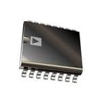
| 供应商器件封装 | 16-TSSOP |
| 分辨率 | 12 bit |
| 包装 | 管件 |
| 商标 | Analog Devices |
| 安装类型 | 表面贴装 |
| 安装风格 | SMD/SMT |
| 封装 | Tube |
| 封装/外壳 | 16-TSSOP(0.173",4.40mm 宽) |
| 封装/箱体 | TSSOP-16 |
| 工作温度 | -40°C ~ 105°C |
| 工厂包装数量 | 96 |
| 建立时间 | 8µs |
| 接口类型 | SPI |
| 数据接口 | DSP,MICROWIRE™,QSPI™,串行,SPI™ |
| 最大功率耗散 | 5 mW |
| 最大工作温度 | + 105 C |
| 最小工作温度 | - 40 C |
| 标准包装 | 1 |
| 电压参考 | External |
| 电压源 | 单电源 |
| 电源电压-最大 | 5.5 V |
| 电源电压-最小 | 2.5 V |
| 积分非线性 | +/- 12 LSB |
| 稳定时间 | 6 us |
| 系列 | AD5328 |
| 结构 | Resistor String |
| 转换器数 | 8 |
| 转换器数量 | 8 |
| 输出数和类型 | 8 电压,单极8 电压,双极 |
| 输出类型 | Voltage |
| 采样比 | 167 kSPs |
| 采样率(每秒) | - |


- 商务部:美国ITC正式对集成电路等产品启动337调查
- 曝三星4nm工艺存在良率问题 高通将骁龙8 Gen1或转产台积电
- 太阳诱电将投资9.5亿元在常州建新厂生产MLCC 预计2023年完工
- 英特尔发布欧洲新工厂建设计划 深化IDM 2.0 战略
- 台积电先进制程称霸业界 有大客户加持明年业绩稳了
- 达到5530亿美元!SIA预计今年全球半导体销售额将创下新高
- 英特尔拟将自动驾驶子公司Mobileye上市 估值或超500亿美元
- 三星加码芯片和SET,合并消费电子和移动部门,撤换高东真等 CEO
- 三星电子宣布重大人事变动 还合并消费电子和移动部门
- 海关总署:前11个月进口集成电路产品价值2.52万亿元 增长14.8%


PDF Datasheet 数据手册内容提取
2.5 V to 5.5 V Octal Voltage Output 8-/10-/12-Bit DACs in 16-Lead TSSOP AD5308/AD5318/AD5328 FEATURES APPLICATIONS AD5308: 8 buffered 8-bit DACs in 16-lead TSSOP Portable battery-powered instruments A version: ±1 LSB INL, B version: ±0.75 LSB INL Digital gain and offset adjustment AD5318: 8 buffered 10-bit DACs in 16-lead TSSOP Programmable voltage and current sources A version: ±4 LSB INL, B version: ±3 LSB INL Optical networking AD5328: 8 buffered 12-bit DACs in 16-lead TSSOP Automatic test equipment A version: ±16 LSB INL, B version: ±12 LSB INL Mobile communications Low power operation: 0.7 mA @ 3 V Programmable attenuators Guaranteed monotonic by design over all codes Industrial process control Power-down to 120 nA @ 3 V, 400 nA @ 5 V Double-buffered input logic Buffered/unbuffered/V reference input options DD Output range: 0 V to V or 0 V to 2 V REF REF Power-on reset to 0 V Programmability Individual channel power-down Simultaneous update of outputs (LDAC) Low power, SPI-®, QSPI-™, MICROWIRE-™, and DSP- compatible 3-wire serial interface On-chip rail-to-rail output buffer amplifiers Temperature range: −40°C to +125°C Qualified for automotive applications GENERAL DESCRIPTION The AD5308/AD5318/AD5328 are octal 8-, 10-, and 12-bit incorporate a power-on reset circuit, which ensures that the buffered voltage output DACs in a 16-lead TSSOP. They operate DAC outputs power up to 0 V and remain there until a valid from a single 2.5 V to 5.5 V supply, consuming 0.7 mA typical write to the device takes place. The outputs of all DACs may be at 3 V. Their on-chip output amplifiers allow the outputs to updated simultaneously using the asynchronous LDAC input. swing rail-to-rail with a slew rate of 0.7 V/μs. The AD5308/ The parts contain a power-down feature that reduces the current AD5318/AD5328 use a versatile 3-wire serial interface that consumption of the devices to 400 nA at 5 V (120 nA at 3 V). operates at clock rates up to 30 MHz and is compatible with The eight channels of the DAC may be powered down individually. standard SPI, QSPI, MICROWIRE, and DSP interface All three parts are offered in the same pinout, which allows standards. users to select the resolution appropriate for their application The references for the eight DACs are derived from two without redesigning their circuit board. reference pins (one per DAC quad). These reference inputs can be configured as buffered, unbuffered, or V inputs. The parts DD Rev. F Information furnished by Analog Devices is believed to be accurate and reliable. However, no responsibility is assumed by Analog Devices for its use, nor for any infringements of patents or other One Technology Way, P.O. Box 9106, Norwood, MA 02062-9106, U.S.A. rights of third parties that may result from its use. Specifications subject to change without notice. No license is granted by implication or otherwise under any patent or patent rights of Analog Devices. Tel: 781.329.4700 www.analog.com Trademarks and registered trademarks are the property of their respective owners. Fax: 781.461.3113 ©2002–2011 Analog Devices, Inc. All rights reserved.
AD5308/AD5318/AD5328 TABLE OF CONTENTS Features..............................................................................................1 Low Power Serial Interface.......................................................18 Applications.......................................................................................1 Load DAC Input (LDAC) Function.........................................18 General Description.........................................................................1 Double-Buffered Interface........................................................18 Revision History...............................................................................2 Microprocessor Interface...............................................................19 Functional Block Diagram..............................................................3 ADSP-2101/ADSP-2103-to-AD5308/AD5318/AD5328 Specifications.....................................................................................4 Interface.......................................................................................19 Absolute Maximum Ratings............................................................7 68HC11/68L11-to-AD5308/AD5318/AD5328 Interface.....19 ESD Caution..................................................................................7 80C51/80L51-to-AD5308/AD5318/AD5328 Interface.........19 Pin Configuration and Function Descriptions.............................8 Microwire-to-AD5308/AD5318/AD5328 Interface..............20 Typical Performance Characteristics.............................................9 Applications Information..............................................................21 Terminology....................................................................................13 Typical Application Circuit.......................................................21 Theory of Operation......................................................................15 Driving VDD from the Reference Voltage................................21 Digital-to-Analog Converter....................................................15 Bipolar Operation Using the AD5308/AD5318/AD5328.....21 Resistor String.............................................................................15 Opto-Isolated Interface for Process Control Applications...21 Output Amplifier........................................................................15 Decoding Multiple AD5308/AD5318/AD5328s....................22 Power-On Reset..........................................................................16 Outline Dimensions.......................................................................24 Power-Down Mode....................................................................16 Ordering Guide..........................................................................24 Serial Interface............................................................................16 REVISION HISTORY 4/11—Rev. E to Rev. F Added Automotive Products Information.................Throughout 2/11—Rev. D to Rev. E Change to Temperature Range....................................Throughout Changes to Table 3, t Timing Characteristics..............................6 4 3/07—Rev. C to Rev. D Updated Format..................................................................Universal Changes to Absolute Maximum Ratings Section.........................7 9/05—Rev. B to Rev. C Updated Format..................................................................Universal Change to Equation........................................................................21 11/03—Rev. A to Rev. B Changes to Ordering Guide............................................................4 Changes to Y axis on TPCs 12, 13, and 15....................................9 8/03—Rev. 0 to Rev. A Added A Version.................................................................Universal Changes to Features..........................................................................1 Changes to Specifications................................................................2 Edits to Absolute Maximum Ratings.............................................4 Edits to Ordering Guide..................................................................4 Updated Outline Dimensions.......................................................18 Rev. F | Page 2 of 28
AD5308/AD5318/AD5328 FUNCTIONAL BLOCK DIAGRAM VDD VREFABCD VDD GAIN-SELECT LOGIC INPUT DAC STRING LDAC REGISTER REGISTER BDUAFCF AER BBUUFFFFEERR VOUTA INPUT STDRAINCG STRING REGISTER REGISTER DAC B BBUUFFFFEERR VOUTB INPUT DAC STRING REGISTER REGISTER DAC C BBUUFFFFEERR VOUTC SCLK INPUT DAC STRING REGISTER REGISTER DAC D BBUUFFFFEERR VOUTD INTERFACE SYNC LOGIC INPUT DAC STRING REGISTER REGISTER DAC E BBUUFFFFEERR VOUTE DIN REINGPISUTTER REGDIASCTER SDTARCIN FG BBUUFFFFEERR VOUTF REINGPISUTTER REGDIASCTER SDTARCIN GG BBUUFFFFEERR VOUTG REINGRPISEUTSTEERT REGDIASCTER DSDDTARCIN HG BBUUFFFFEERR VOUTH GND POWER-ON GAIN-SELECT POWER-DOWN RESET VDD LOGIC LOGIC 02812-001 LDAC VREFEFGH GND Figure 1. Rev. F | Page 3 of 28
AD5308/AD5318/AD5328 SPECIFICATIONS V = 2.5 V to 5.5 V; V = 2 V; R = 2 kΩ to GND; C = 200 pF to GND; all specifications T to T , unless otherwise specified. DD REF L L MIN MAX Table 1. A Version1 B Version1 Parameter2 Min Typ Max Min Typ Max Unit Conditions/Comments DC PERFORMANCE3, 4 AD5308 Resolution 8 8 Bits Relative Accuracy ±0.15 ±1 ±0.15 ±0.75 LSB Differential Nonlinearity ±0.02 ±0.25 ±0.02 ±0.25 LSB Guaranteed monotonic by design over all codes AD5318 Resolution 10 10 Bits Relative Accuracy ±0.5 ±4 ±0.5 ±3 LSB Differential Nonlinearity ±0.05 ±0.50 ±0.05 ±0.50 LSB Guaranteed monotonic by design over all codes AD5328 Resolution 12 12 Bits Relative Accuracy ±2 ±16 ±2 ±12 LSB Differential Nonlinearity ±0.2 ±1.0 ±0.2 ±1.0 LSB Guaranteed monotonic by design over all codes Offset Error ±5 ±60 ±5 ±60 mV V = 4.5 V, gain = 2, see DD Figure 27 and Figure 28 Gain Error ±0.30 ±1.25 ±0.30 ±1.25 % of FSR V = 4.5 V, gain = 2, see DD Figure 27 and Figure 28 Lower Deadband5 10 60 10 60 mV Lower deadband exists only if offset error is negative, see Figure 27 Upper Deadband5 10 60 10 60 mV Upper deadband exists only if V = V and offset plus REF DD gain error is positive, see Figure 28 Offset Error Drift6 −12 −12 ppm of FSR/°C Gain Error Drift6 −5 −5 ppm of FSR/°C DC Power Supply Rejection Ratio6 −60 −60 dB VDD = ±10% DC Crosstalk6 200 200 μV RL = 2 kΩ to GND or VDD DAC REFERENCE INPUTS6 V Input Range 1.0 V 1.0 V V Buffered reference mode REF DD DD 0.25 V 0.25 V V Unbuffered reference mode DD DD V Input Impedance (R ) >10.0 >10.0 MΩ Buffered reference mode REF DAC and power-down mode 37.0 45.0 37.0 45.0 kΩ Unbuffered reference mode, 0 V to V output range REF 18.0 22.0 18.0 22.0 kΩ Unbuffered reference mode, 0 V to 2 V output range REF Reference Feedthrough −70.0 −70.0 dB Frequency = 10 kHz Channel-to-Channel Isolation −75.0 −75.0 dB Frequency = 10 kHz OUTPUT CHARACTERISTICS6 Minimum Output Voltage7 0.001 0.001 V This is a measure of the minimum and maximum Maximum Output Voltage7 VDD − VDD − 0.001 V Drive capability of the 0.001 output amplifier DC Output Impedance 0.5 0.5 Ω Rev. F | Page 4 of 28
AD5308/AD5318/AD5328 A Version1 B Version1 Parameter2 Min Typ Max Min Typ Max Unit Conditions/Comments Short Circuit Current 25.0 25.0 mA V = 5 V DD 16.0 16.0 mA V = 3 V DD Power-Up Time 2.5 2.5 μs Coming out of power-down mode, V = 5 V DD 5.0 5.0 μs Coming out of power-down mode, V = 3 V DD LOGIC INPUTS6 Input Current ±1 ±1 μA V , Input Low Voltage 0.8 0.8 V V = 5 V ± 10% IL DD 0.8 0.8 V V = 3 V ± 10% DD 0.7 0.7 V V = 2.5 V DD V , Input High Voltage 1.7 1.7 V V = 2.5 V to 5.5 V, TTL and IH DD CMOS compatible Pin Capacitance 3.0 3.0 pF POWER REQUIREMENTS V 2.5 5.5 2.5 5.5 V DD I (Normal Mode)8 V = V and V = GND DD IH DD IL V = 4.5 V to 5.5 V 1.0 1.8 1.0 1.8 mA All DACs in unbuffered DD mode, in buffered mode V = 2.5 V to 3.6 V 0.7 1.5 0.7 1.5 mA Extra current is typically x μA DD per DAC; x = (5 μA + V /R )/4 REF DAC I (Power-Down Mode)9 V = V and V = GND DD IH DD IL V = 4.5 V to 5.5 V 0.4 1 0.4 1 μA DD V = 2.5 V to 3.6 V 0.12 1 0.12 1 μA DD 1 Temperature range (A, B version): −40°C to +125°C; typical at 25°C. 2 See the Terminology section. 3 DC specifications tested with the outputs unloaded unless stated otherwise. 4 Linearity is tested using a reduced code range: AD5308 (Code 8 to Code 255), AD5318 (Code 28 to Code 1023), and AD5328 (Code 115 to Code 4095). 5 This corresponds to x codes. x = deadband voltage/LSB size. 6 Guaranteed by design and characterization; not production tested. 7 For the amplifier output to reach its minimum voltage, offset error must be negative. For the amplifier output to reach its maximum voltage, VREF = VDD and offset plus gain error must be positive. 8 Interface inactive. All DACs active. DAC outputs unloaded. 9 All eight DACs powered down. V = 2.5 V to 5.5 V; R = 2 kΩ to GND; C = 200 pF to GND; all specifications T to T , unless otherwise noted. DD L L MIN MAX Table 2. AC Characteristics1 A, B Version2 Parameter3 Min Typ Max Unit Conditions/Comments Output Voltage Settling Time V = V = 5 V REF DD AD5308 6 8 μs 1/4 scale to 3/4 scale change (0x40 to 0xC0) AD5318 7 9 μs 1/4 scale to 3/4 scale change (0x100 To 0x300) AD5328 8 10 μs 1/4 scale to 3/4 scale change (0x400 to 0xC00) Slew Rate 0.7 V/μs Major-Code Change Glitch Energy 12 nV-sec 1 LSB change around major carry Digital Feedthrough 0.5 nV-sec Digital Crosstalk 0.5 nV-sec Analog Crosstalk 1 nV-sec DAC-to-DAC Crosstalk 3 nV-sec Multiplying Bandwidth 200 kHz V = 2 V ± 0.1 V p-p, unbuffered mode REF Total Harmonic Distortion −70 dB V = 2.5 V ± 0.1 V p-p, frequency = 10 kHz REF 1 Guaranteed by design and characterization; not production tested. 2 Temperature range (A, B version): –40°C to +125°C; typical at 25°C. 3 See the Terminology section. Rev. F | Page 5 of 28
AD5308/AD5318/AD5328 Table 3. Timing Characteristics1, 2, 3 A, B Version Parameter Limit at T , T Unit Conditions/Comments MIN MAX t 33 ns min SCLK cycle time 1 t 13 ns min SCLK high time 2 t 13 ns min SCLK low time 3 t 13 ns min SYNC to SCLK falling edge setup time; temperature range (A, B 4 verstion): −40°C to +105°C 15 ns min SYNC to SCLK falling edge setup time; temperature range (A, B verstion): −40°C to +125°C t 5 ns min Data set up time 5 t 4.5 ns min Data hold time 6 t 0 ns min SCLK falling edge to SYNC rising edge 7 t 50 ns min Minimum SYNC high time 8 t 20 ns min LDAC pulse width 9 t 20 ns min SCLK falling edge to LDAC rising edge 10 t 0 ns min SCLK falling edge to LDAC falling edge 11 1 Guaranteed by design and characterization; not production tested. 2 All input signals are specified with tR = tF = 5 ns (10% to 90% of VDD) and timed from a voltage level of (VIL + VIH)/2. 3 See Figure 2. t 1 SCLK t t8 t t3 2 t7 4 SYNC t 6 t 5 DIN DB15 DB0 t 9 t 11 LDAC1 t LDAC2 10 02812-002 NOTES 1ASYNCHRONOUS LDAC UPDATE MODE. 2SYNCHRONOUS LDAC UPDATE MODE. Figure 2. Serial Interface Timing Diagram Rev. F | Page 6 of 28
AD5308/AD5318/AD5328 ABSOLUTE MAXIMUM RATINGS Stresses above those listed under Absolute Maximum Ratings T = 25°C, unless otherwise specified. A may cause permanent damage to the device. This is a stress Table 4. rating only; functional operation of the device at these or any Parameter Rating1 other conditions above those indicated in the operational V to GND −0.3 V to +7 V section of this specification is not implied. Exposure to absolute DD Digital Input Voltage to GND −0.3 V to V + 0.3 V maximum rating conditions for extended periods may affect DD Reference Input Voltage to GND −0.3 V to V + 0.3 V device reliability. DD VOUTA–VOUTD to GND −0.3 V to VDD + 0.3 V Operating Temperature Range ESD CAUTION Industrial (A, B Version) −40°C to +125°C Storage Temperature Range −65°C to +150°C Junction Temperature (T ) 150°C J MAX 16-Lead TSSOP Power Dissipation (T − T )/θ J MAX A JA θJA Thermal Impedance 150.4°C/W Lead Temperature JEDEC industry-standard Soldering J-STD-020 1 Transient currents of up to 100 mA do not cause SCR latch-up. Rev. F | Page 7 of 28
AD5308/AD5318/AD5328 PIN CONFIGURATION AND FUNCTION DESCRIPTIONS LDAC 1 16 SCLK SYNC 2 15 DIN VDD 3 AD5308/ 14 GND AD5318/ VOUTA 4 AD5328 13 VOUTH VOUTB 5 12 VOUTG TOP VIEW VOUTC 6 (Not to Scale) 11 VOUTF VOUTD 7 10 VOUTE VREFABCD 8 9 VREFEFGH 02812-003 Figure 3. Pin Configuration Table 5. Pin Function Descriptions Pin No. Mnemonic Description 1 LDAC This active low control input transfers the contents of the input registers to their respective DAC registers. Pulsing this pin low allows any or all DAC registers to be updated if the input registers have new data. This allows simul- taneous updates of all DAC outputs. Alternatively, this pin can be tied permanently low. 2 SYNC Active Low Control Input. This is the frame synchronization signal for the input data. When SYNC goes low, it powers on the SCLK and DIN buffers and enables the input shift register. Data is transferred in on the falling edges of the following 16 clocks. If SYNC is taken high before the 16th falling edge, the rising edge of SYNC acts as an interrupt and the write sequence is ignored by the device. 3 V Power Supply Input. These parts can be operated from 2.5 V to 5.5 V, and the supply should be decoupled with a 10 μF DD capacitor in parallel with a 0.1 μF capacitor to GND. 4 V A Buffered Analog Output Voltage from DAC A. The output amplifier has rail-to-rail operation. OUT 5 V B Buffered Analog Output Voltage from DAC B. The output amplifier has rail-to-rail operation. OUT 6 V C Buffered Analog Output Voltage from DAC C. The output amplifier has rail-to-rail operation. OUT 7 V D Buffered Analog Output Voltage from DAC D. The output amplifier has rail-to-rail operation. OUT 8 V ABCD Reference Input Pin for DACs A, B, C, and D. It can be configured as a buffered, unbuffered, or V input to the four REF DD DACs, depending on the state of the BUF and V control bits. It has an input range from 0.25 V to V in unbuffered DD DD mode and from 1 V to V in buffered mode. DD 9 V EFGH Reference Input Pin for DACs E, F, G, and H. It can be configured as a buffered, unbuffered, or V input to the four REF DD DACs, depending on the state of the BUF and V control bits. It has an input range from 0.25 V to V in unbuffered DD DD mode and from 1 V to V in buffered mode. DD 10 V E Buffered Analog Output Voltage from DAC E. The output amplifier has rail-to-rail operation. OUT 11 V F Buffered Analog Output Voltage from DAC F. The output amplifier has rail-to-rail operation. OUT 12 V G Buffered Analog Output Voltage from DAC G. The output amplifier has rail-to-rail operation. OUT 13 V H Buffered Analog Output Voltage from DAC H. The output amplifier has rail-to-rail operation. OUT 14 GND Ground Reference Point for All Circuitry on the Part. 15 DIN Serial Data Input. This device has a 16-bit shift register. Data is clocked into the register on the falling edge of the serial clock input. The DIN input buffer is powered down after each write cycle. 16 SCLK Serial Clock Input. Data is clocked into the input shift register on the falling edge of the serial clock input. Data can be transferred at rates up to 30 MHz. The SCLK input buffer is powered down after each write cycle. Rev. F | Page 8 of 28
AD5308/AD5318/AD5328 TYPICAL PERFORMANCE CHARACTERISTICS 1.0 0.3 VTAD D= =2 55°VC TVAD D= =2 55°VC 0.2 0.5 INL ERROR (LSB) 0 DNL ERROR (LSB) –00..011 –0.5 –0.2 –1.0 –0.3 02812-009 0 50 100 CODE150 200 250 02812-006 0 50 100 CODE150 200 250 Figure 4. AD5308 Typical INL Plot Figure 7. AD5308 Typical DNL Plot 3 0.6 TA = 25°C TA = 25°C VDD = 5V VDD = 5V 2 0.4 INL ERROR (LSB) –101 DNL ERROR (LSB) –00..022 –2 –0.4 –3 02812-007 –0.6 02812-010 0 200 400 600 800 1000 0 200 400 600 800 1000 CODE CODE Figure 5. AD5318 Typical INL Plot Figure 8. AD5318 Typical DNL Plot 12 1.0 TA = 25°C TA = 25°C VDD = 5V VDD = 5V 8 0.5 B) 4 B) S S R (L R (L RO 0 RO 0 R R E E INL –4 DNL –0.5 –8 –12 02812-008 –1.0 02812-011 0 500 1000 1500 2000 2500 3000 3500 4000 0 500 1000 1500 2000 2500 3000 3500 4000 CODE CODE Figure 6. AD5328 Typical INL Plot Figure 9. AD5328 Typical DNL Plot Rev. F | Page 9 of 28
AD5308/AD5318/AD5328 0.50 0.2 TA = 25°C TA = 25°C VDD = 5V 0.1 VREF = 2V MAX INL 0.25 0 GAIN ERROR OR (LSB) 0 MAX DNL R (% FSR) ––00..21 R O R R E R –0.3 MIN DNL E OFFSET ERROR –0.25 –0.4 MIN INL –0.50 02812-012 ––00..65 02812-015 0 1 2 3 4 5 0 1 2 3 4 5 6 VREF (V) VDD (V) Figure 10. AD5308 INL and DNL Error vs. VREF Figure 13. Offset Error and Gain Error vs. VDD 0.5 5 0.4 VREF = 3V VDD = 5V MAX INL 0.3 4 5V SOURCE 0.2 3V SOURCE SB) 0.1 MAX DNL 3 OR (L 0 (V)UT R O ER –0.1 V 2 MIN DNL –0.2 –0.3 1 5V SINK 3V SINK MIN INL ––00..45 02812-013 0 02812-016 – 40 0 40 80 120 0 1 2 3 4 5 6 TEMPERATURE (°C) SINK/SOURCE CURRENT (mA) Figure 11. AD5308 INL Error and DNL Error vs. Temperature Figure 14. VOUT Source and Sink Current Capability 1.0 1.0 VDD = 5V 0.9 VREF = 2V TA = 25°C 0.8 VDD = 5V 0.5 0.7 SR) GAIN ERROR 0.6 % F mA) R ( 0 (D 0.5 O D RR OFFSET ERROR I 0.4 E 0.3 –0.5 0.2 –1.0 02812-014 0.01 02812-017 –40 0 40 80 120 ZERO SCALE HALF SCALE FULL SCALE DAC CODE TEMPERATURE (°C) Figure 12. AD5308 Offset Error and Gain Error vs. Temperature Figure 15. Supply Current vs. DAC Code Rev. F | Page 10 of 28
AD5308/AD5318/AD5328 1.3 TA = 25°C TA = 25°C 1.2 BVRUEFFF =E R2VE,D GAIN = +1, VVDRDEF = = 5 5VV 1.1 VREF = VDD VOUTA A) 1.0 m CH1 ( D D I 0.9 SCLK CH2 0.8 VREF = 2V, GAIN = +1, UNBUFFERED 00..67 VREF = VDD, GAIN = +1, UNBUFFERED 02812-018 02812-021 2.0 2.5 3.0 3.5 4.0 4.5 5.0 CH1 1V, CH2 5V, TIME BASE = 1μs/DIV SUPPLY VOLTAGE (V) Figure 16. Supply Current vs. Supply Voltage Figure 19. Half-Scale Settling (1/4 to 3/4 Scale Code Change) 1.0 TA = 25°C 0.9 TA = 25°C VDD = 5V VREF = 2V 0.8 A) μ N ( 0.7 W DO 0.6 VDD R- CH1 WE 0.5 O P 0.4 D D I 0.3 0.2 VOUTA 0.10 02812-019 CH2 02812-022 2.0 2.5 3.0 3.5 4.0 4.5 5.0 5.5 CH1 2.00V, CH2 200mV, TIME BASE = 200μs/DIV VDD (V) Figure 17. Power-Down Current vs. Supply Voltage Figure 20. Power-On Reset to 0 V 1.4 1.3 DECREASING INCREASING VTAD D= =2 55°VC VTVADR DE=F = 2= 55 °2VCV 1.2 A) 1.1 m VOUTA ( IDD 1.0 CH1 0.9 0.8 PD 00..67 VDD = 3V 02812-020 CH2 CH1 500V, CH2 5.00mV, TIME BASE = 1μs/DIV 02812-023 0 0.5 1.0 1.5 2.0 2.5 3.0 3.5 4.0 4.5 5.0 VLOGIC (V) Figure 18. Supply Current vs. Logic Input Voltage for SCLK and DIN Increasing Figure 21. Exiting Power-Down to Midscale and Decreasing Rev. F | Page 11 of 28
AD5308/AD5318/AD5328 35 0.02 SS = 300 TA = 25°C 30 VDD = 3V VDD = 5V VDD = 5V V) QUENCY2250 MMEEAANN:: 01..60923075958 E ERROR ( 0.01 FRE SCAL 0 15 L- L U F 10 –0.01 5 0 02812-024 –0.02 02812-027 0.6 0.7 0.8 0.9 1.0 1.1 0 1 2 3 4 5 6 IDD (mA) VREF(V) Figure 22. IDD Histogram with VDD = 3 V and VDD = 5 V Figure 25. Full-Scale Error vs. VREF 2.50 2.49 (V)OUT mV/DIV V 1 2.48 2.47 02812-025 02812-028 1μs/DIV 100ns/DIV Figure 23. AD5328 Major-Code Transition Glitch Energy Figure 26. DAC-to-DAC Crosstalk 10 0 –10 –20 B) d ( –30 –40 –50 –60 02812-026 10 100 1k 10k 100k 1M 10M FREQUENCY (Hz) Figure 24. Multiplying Bandwidth (Small-Signal Frequency Response) Rev. F | Page 12 of 28
AD5308/AD5318/AD5328 TERMINOLOGY Relative Accuracy Major-Code Transition Glitch Energy For the DAC, relative accuracy or integral nonlinearity (INL) is Major-code transition glitch energy is the energy of the impulse a measure of the maximum deviation, in LSB, from a straight injected into the analog output when the code in the DAC line passing through the endpoints of the DAC transfer func- register changes state. It is normally specified as the area of the tion. Typical INL vs. code plots can be seen in Figure 4, Figure 5, glitch in nV-sec and is measured when the digital code is and Figure 6. changed by 1 LSB at the major carry transition (011 ... 11 to 100 ... 00 or 100 ... 00 to 011 ... 11). Differential Nonlinearity Differential nonlinearity (DNL) is the difference between the Digital Feedthrough measured change and the ideal 1 LSB change between any two Digital feedthrough is a measure of the impulse injected into adjacent codes. A specified differential nonlinearity of ±1 LSB the analog output of a DAC from the digital input pins of the maximum ensures monotonicity. This DAC is guaranteed device, but is measured when the DAC is not being written to monotonic by design. Typical DNL vs. code plots can be seen (SYNC held high). It is specified in nV-sec and is measured in Figure 7, Figure 8, and Figure 9. with a full-scale change on the digital input pins, that is, from Offset Error all 0s to all 1s and vice versa. This is a measure of the offset error of the DAC and the output Digital Crosstalk amplifier (see Figure 27 and Figure 28). It can be negative or This is the glitch impulse transferred to the output of one DAC positive, and is expressed in millivolts. at midscale in response to a full-scale code change (all 0s to all Gain Error 1s and vice versa) in the input register of another DAC. It is measured in standalone mode and is expressed in nV-sec. This is a measure of the span error of the DAC. It is the devia- tion in slope of the actual DAC transfer characteristic from the Analog Crosstalk ideal expressed as a percentage of the full-scale range. This is the glitch impulse transferred to the output of one DAC Offset Error Drift due to a change in the output of another DAC. It is measured by This is a measure of the change in offset error with changes in loading one of the input registers with a full-scale code change temperature. It is expressed in (ppm of full-scale range)/°C. (all 0s to all 1s and vice versa) while keeping LDAC high. Then pulse LDAC low and monitor the output of the DAC whose digital Gain Error Drift code is not changed. The area of the glitch is expressed in nV-sec. This is a measure of the change in gain error with changes in temperature. It is expressed in (ppm of full-scale range)/°C. DAC-to-DAC Crosstalk This is the glitch impulse transferred to the output of one DAC DC Power Supply Rejection Ratio (PSRR) due to a digital code change and subsequent output change of This indicates how the output of the DAC is affected by changes another DAC. This includes both digital and analog crosstalk. in the supply voltage. PSRR is the ratio of the change in V to OUT It is measured by loading one of the DACs with a full-scale code a change in V for full-scale output of the DAC. It is measured DD change (all 0s to all 1s and vice versa) with LDAC low and in decibels. V is held at 2 V and V is varied ±10%. REF DD monitoring the output of another DAC. The energy of the glitch DC Crosstalk is expressed in nV-sec. This is the dc change in the output level of one DAC in response Multiplying Bandwidth to a change in the output of another DAC. It is measured with a The amplifiers within the DAC have a finite bandwidth. The full-scale output change on one DAC while monitoring another multiplying bandwidth is a measure of this. A sine wave on the DAC. It is expressed in microvolts. reference (with full-scale code loaded to the DAC) appears on Reference Feedthrough the output. The multiplying bandwidth is the frequency at This is the ratio of the amplitude of the signal at the DAC out- which the output amplitude falls to 3 dB below the input. put to the reference input when the DAC output is not being Total Harmonic Distortion (THD) updated (that is, LDAC is high). It is expressed in decibels. This is the difference between an ideal sine wave and its atten- Channel-to-Channel Isolation uated version using the DAC. The sine wave is used as the refer- This is the ratio of the amplitude of the signal at the output of ence for the DAC and the THD is a measure of the harmonics one DAC to a sine wave on the reference input of another DAC. present on the DAC output. It is measured in decibels. It is measured in decibels. Rev. F | Page 13 of 28
AD5308/AD5318/AD5328 GAIN ERROR PLUS GAIN ERROR OFFSET ERROR PLUS OFFSET ERROR OUTPUT UPPER VOLTAGE OUTPUT ACTUAL DEADBAND VOLTAGE CODES IDEAL NEGATIVE OFFSET DAC CODE POSITIVE ERROR IADCETAULAL OEFRFRSOERT DAC CODE FULL SCALE 02812-005 Figure 28. Transfer Function with Positive Offset LOWER DEADBAND CODES AMPLIFIER FOOTROOM NEGATIVE OFFSET ERROR 02812-004 Figure 27. Transfer Function with Negative Offset (VREF = VDD) Rev. F | Page 14 of 28
AD5308/AD5318/AD5328 THEORY OF OPERATION If there is a buffered reference in the circuit (for example, the The AD5308/AD5318/AD5328 are octal resistor-string DACs REF192), there is no need to use the on-chip buffers of the fabricated on a CMOS process with resolutions of 8, 10, and AD5308/AD5318/AD5328. In unbuffered mode, the input 12 bits, respectively. Each contains eight output buffer ampli- impedance is still large at typically 45 kΩ per reference input fiers and is written to via a 3-wire serial interface. They operate for 0 V to V mode and 22 kΩ for 0 V to 2 V mode. from single supplies of 2.5 V to 5.5 V and the output buffer REF REF amplifiers provide rail-to-rail output swing with a slew rate of RESISTOR STRING 0.7 V/μs. DAC A, DAC B, DAC C, and DAC D share a common The resistor-string section is shown in Figure 30. It is simply a reference input, V ABCD. DAC E, DAC F, DAC G, and DAC H REF string of resistors, each of value R. The digital code loaded to share a common reference input, V EFGH. Each reference REF the DAC register determines at which node on the string the input can be buffered to draw virtually no current from the voltage is tapped off to be fed into the output amplifier. The reference source, can be unbuffered to give a reference input voltage is tapped off by closing one of the switches connecting range from 0.25 V to V , or can come from V . The devices DD DD the string to the amplifier. Because it is a string of resistors, it is have a power-down mode in which all DACs can be turned off guaranteed monotonic. individually with a high impedance output. DIGITAL-TO-ANALOG CONVERTER R The architecture of one DAC channel consists of a resistor R string DAC followed by an output buffer amplifier. The voltage TO OUTPUT at the VREF pin provides the reference voltage for the corre- R AMPLIFIER sponding DAC. Figure 29 shows a block diagram of the DAC architecture. Since the input coding to the DAC is straight binary, the ideal output voltage is given by V ×D R V = REF OUT 2N R where: 02812-030 D is the decimal equivalent of the binary code that is loaded to Figure 30. Resistor String the DAC register: OUTPUT AMPLIFIER 0 to 255 for AD5308 (8 bits) The output buffer amplifier is capable of generating output 0 to 1023 for AD5318 (10 bits) voltages to within 1 mV of either rail. Its actual range depends 0 to 4095 for AD5328 (12 bits) on the value of V , the gain of the output amplifier, the offset N is the DAC resolution. REF error, and the gain error. VREFABCD VDD If a gain of 1 is selected (gain bit = 0), the output range is REFERENCE 0.001 V to V . VDD BUF BUFFER (GAGINA I=N +M1O ODRE +2) REF If a gain of 2 is selected (gain bit = 1), the output range is 0.001 V to 2 V . Because of clamping, however, the maximum REF REINGPISUTTER REGDIASCTER RSETSRISINTOGR VOUTA output is limited to VDD − 0.001 V. The output amplifier is capable of driving a load of 2 kΩ to BUFFEORU TAPMUPTLIFIER 02812-029 sGoNurDce o arn VdD sDi,n ikn cpaapraabllielli twieist ho f5 t0h0e p oFu ttpou Gt NamDp olirf iVerD Dc.a nT hbee seen Figure 29. Single DAC Channel Architecture in the plot in Figure 14. DAC Reference Inputs The slew rate is 0.7 V/μs with a half-scale settling time to There is a reference pin for each quad of DACs. The reference ±0.5 LSB (at 8 bits) of 6 μs. inputs can be buffered from V , or unbuffered. The advantage DD with the buffered input is the high impedance it presents to the voltage source driving it. However, if the unbuffered mode is used, the user can have a reference voltage as low as 0.25 V and as high as V since there is no restriction due to the headroom DD and footroom of the reference amplifier. Rev. F | Page 15 of 28
AD5308/AD5318/AD5328 POWER-ON RESET SERIAL INTERFACE The AD5308/AD5318/AD5328 are provided with a power-on The AD5308/AD5318/AD5328 are controlled over a versatile reset function so that they power up in a defined state. The 3-wire serial interface that operates at clock rates up to 30 MHz power-on state is and is compatible with SPI, QSPI, MICROWIRE, and DSP interface standards. • Normal operation Input Shift Register • Reference inputs unbuffered The input shift register is 16 bits wide. Data is loaded into the • 0 V to V output range REF device as a 16-bit word under the control of a serial clock input, • Output voltage set to 0 V SCLK. The timing diagram for this operation is shown in Figure 2. • LDAC bits set to LDAC high The SYNC input is a level-triggered input that acts as a frame synchronization signal and chip enable. Data can be transferred Both input and DAC registers are filled with 0s and remain so into the device only while SYNC is low. To start the serial data until a valid write sequence is made to the device. This is particularly useful in applications where it is important to know transfer, SYNC should be taken low, observing the minimum the state of the DAC outputs while the device is powering up. SYNC to SCLK falling edge set-up time, t4. After SYNC goes low, serial data is shifted into the device’s input shift register on POWER-DOWN MODE the falling edges of SCLK for 16 clock pulses. The AD5308/AD5318/AD5328 have low power consumption, To end the transfer, SYNC must be taken high after the falling typically dissipating 2.4 mW with a 3 V supply and 5 mW with edge of the 16th SCLK pulse, observing the minimum SCLK a 5 V supply. Power consumption can be further reduced when falling edge to SYNC rising edge time, t. the DACs are not in use by putting them into power-down 7 mode, which is described in the Serial Interface section. After the end of the serial data transfer, data is automatically transferred from the input shift register to the input register of When in default mode, all DACs work normally with a typical the selected DAC. If SYNC is taken high before the 16th falling power consumption of 1 mA at 5 V (800 μA at 3 V). However, when all DACs are powered down, that is, in power-down edge of SCLK, the data transfer is aborted and the DAC input mode, the supply current falls to 400 nA at 5 V (120 nA at 3 V). registers are not updated. Not only does the supply current drop, but the output stage is Data is loaded MSB first (Bit 15). The first bit determines also internally switched from the output of the amplifier, whether it is a DAC write or a control function. making it open-circuit. This has the advantage that the output is DAC Write three-state while the part is in power-down mode, and provides The 16-bit word consists of 1 control bit and 3 address bits fol- a defined input condition for whatever is connected to the lowed by 8, 10, or 12 bits of DAC data, depending on the device output of the DAC amplifier. The output stage is illustrated in type. In the case of a DAC write, the MSB is a 0. The next 3 Figure 31. address bits determine whether the data is for DAC A, DAC B, The bias generator, the output amplifiers, the resistor string, and DAC C, DAC D, DAC E, DAC F, DAC G, or DAC H. The all other associated linear circuitry are shut down when the AD5328 uses all 12 bits of DAC data. The AD5318 uses 10 bits power-down mode is activated. However, the contents of the and ignores the 2 LSBs. The AD5308 uses 8 bits and ignores the registers are unaffected when in power-down. In fact, it is last 4 bits. These ignored LSBs should be set to 0. The data possible to load new data to the input registers and DAC regis- format is straight binary, with all 0s corresponding to 0 V ters during power-down. The DAC outputs update as soon as output and all 1s corresponding to full-scale output. the device comes out of power-down mode. The time to exit power-down is typically 2.5 μs when V = 5 V and 5 μs when Table 6. Address Bits for the AD5308/AD5318/AD5328 DD VDD = 3 V. A2 (Bit 14) A1 (Bit 13) A0 (Bit 12) DAC Addressed 0 0 0 DAC A AMPLIFIER 0 0 1 DAC B RESISTOR- STRING DAC VOUT 0 1 0 DAC C 0 1 1 DAC D POCWIRECRU-IDTORWYN 02812-035 11 00 10 DDAACC FE Figure 31. Output Stage During Power-Down 1 1 0 DAC G 1 1 1 DAC H Rev. F | Page 16 of 28
AD5308/AD5318/AD5328 Control Functions BUF In the case of a control function, the MSB (Bit 15) is a 1. This is This controls whether the reference of a group of DACs is followed by two control bits, which determine the mode. There buffered or unbuffered. The reference of the first group of DACs are four different control modes: reference and gain mode, LDAC (A, B, C, and D) is controlled by setting Bit 2, and the second mode, power-down mode, and reset mode. The write sequences group of DACs (E, F, G, and H) is controlled by setting Bit 3. for these modes are shown in Table 7. 0: unbuffered reference. Reference and Gain Mode 1: buffered reference. This mode determines whether the reference for each group of GAIN DACs is buffered, unbuffered, or from V . It also determines DD The gain of the DACs is controlled by setting Bit 4 for the first the gain of the output amplifier. To set up the reference of both group of DACs (A, B, C, and D) and Bit 5 for the second group groups, set the control bits to (00), set the GAIN bits, the BUF of DACs (E, F, G, and H). bits, and the V bits. DD 0: output range of 0 V to V . REF 1: output range of 0 V to 2 V . REF Table 7. Control Words for the AD53x8 D/C Control Bits 15 14 13 12 11 10 9 8 7 6 5 4 3 2 1 0 Mode GAIN Bits BUF Bits V Bits Gain of output amplifier and DD 1 0 0 x x x x x x x E...H A...D E...H A...D E...H A...D reference selection LDAC Bits 1 0 1 x x x x x x x x x x x 1/0 1/0 LDAC Channels 1 1 0 x x x x x H G F E D C B A Power-down Reset 1 1 1 1/0 x x x x x x x x x x x x Reset BIT 15 BIT 0 LDAC Mode (MSB) (LSB) D/C A2 A1 A0 D7 D6 D5DADT4A BDI3TS D2 D1 D0 0 0 0 0 02812-031 LtrDanAsCfe rmreodd efr coomn ttrhoel si nLpDuAt Cre,g wishteicrsh tdoe ttherem DiAneCs rwehgiesnte drsa.t aT hise re Figure 32. AD5308 Input Shift Register Contents are three options when updating the DAC registers, as shown in BIT 15 BIT 0 Table 8. (MSB) (LSB) D/C A2 A1 A0 D9 D8 D7 D6 D5 D4 D3 D2 D1 D0 0 0 Table 8. LDAC Mode DATA BITS 02812-032 Bit 15 Bit 14 Bit 13 Bits 12:2 Bit 1 Bit 0 Description Figure 33. AD5318 Input Shift Register Contents 1 0 1 x ... x 0 0 LDAC low BIT 15 BIT 0 1 0 1 x ... x 0 1 LDAC high (MSB) (LSB) 1 0 1 x ... x 1 0 LDAC single D/C A2 A1 A0 D11 D10 D9 D8 D7DADT6A BDIT5S D4 D3 D2 D1 D0 02812-033 1 0 1 x ... x 1 1 Ruepsdeartvee d Figure 34. AD5328 Input Shift Register Contents LDAC Low (00): This option sets LDAC permanently low, V DD allowing the DAC registers to be updated continuously. These bits are set when V is to be used as a reference. The DD LDAC High (01): This option sets LDAC permanently high. first group of DACs (A, B, C, and D) can be set up to use V by DD The DAC registers are latched and the input registers can setting Bit 0, and the second group of DACs (E, F, G, and H) by change without affecting the contents of the DAC registers. setting Bit 1. The V bits have priority over the BUF bits. DD This is the default option for this mode. When V is used as the reference, it is always unbuffered and DD LDAC Single Update (10): This option causes a single pulse on has an output range of 0 V to V regardless of the state of the REF LDAC, updating the DAC registers once. GAIN and BUF bits. Reserved (11): reserved. Rev. F | Page 17 of 28
AD5308/AD5318/AD5328 Power-Down Mode Use of the LDAC function enables double-buffering of the DAC data, and the GAIN, BUF and V bits. There are two ways in The individual channels of the AD5308/AD5318/AD5328 can DD which the LDAC function can operate: be powered down separately. The control mode for this is (10). On completion of this write sequence, the channels that have Synchronous LDAC: The DAC registers are updated after new been set to 1 are powered down. data is read in on the falling edge of the 16th SCLK pulse. Reset Mode LDAC can be permanently low or pulsed as in Figure 2. This mode consists of two possible reset functions, as outlined Asynchronous LDAC: The outputs are not updated at the same in Table 9. time that the input registers are written to. When LDAC goes low, the DAC registers are updated with the contents of the Table 9. Reset Mode input register. Bit 15 Bit 14 Bit 13 Bit 12 Bit 11 ... 0 Description DOUBLE-BUFFERED INTERFACE 1 1 1 0 x ... x DAC data reset 1 1 1 1 x ... x Data and control reset The AD5308/AD5318/AD5328 DACs all have double-buffered DAC Data Reset: On completion of this write sequence, all interfaces consisting of two banks of registers: input and DAC. DAC registers and input registers are filled with 0s. The input registers are connected directly to the input shift register and the digital code is transferred to the relevant input Data and Control Reset: This function carries out a DAC data register on completion of a valid write sequence. The DAC reset and resets all the control bits (GAIN, BUF, V , LDAC, and DD registers contain the digital code used by the resistor strings. power-down channels) to their power-on conditions. When the LDAC pin is high and the LDAC bits are set to (01), LOW POWER SERIAL INTERFACE the DAC registers are latched and the input registers can change To minimize the power consumption of the device, the interface state without affecting the contents of the DAC registers. How- powers up fully only when the device is being written to, that is, ever, when the LDAC bits are set to (00) or when the LDAC pin on the falling edge of SYNC. The SCLK and DIN input buffers is brought low, the DAC registers become transparent and the are powered down on the rising edge of SYNC. contents of the input registers are transferred to them. LOAD DAC INPUT (LDAC) FUNCTION The double-buffered interface is useful if the user requires simultaneous updating of all DAC outputs. The user can write Access to the DAC registers is controlled by both the LDAC pin up to seven of the input registers individually and then, by and the LDAC mode bits. The operation of the LDAC function bringing LDAC low when writing to the remaining DAC input can be likened to the configuration shown in Figure 35. register, all outputs will update simultaneously. EXTERNAL LDAC PIN LDAC FUNCTION These parts contain an extra feature whereby a DAC register is INTERNAL LDAC MODE 02812-034 nlaostt utipmdea tLeDd AuCnl ewsass i tlso win. pNuot rrmegailsltye,r w hhaesn b LeeDnA uCp disa tberdo usignhcte l othwe, Figure 35. LDAC Function the DAC registers are filled with the contents of the input regis- If the user wishes to update the DAC through software, the ters. In the case of the AD5308/AD5318/AD5328, the part LDAC pin should be tied high and the LDAC mode bits set as updates the DAC register only if the input register has been required. Alternatively, if the user wishes to control the DAC changed since the last time the DAC register was updated, through hardware, that is, the LDAC pin, the LDAC mode bits thereby removing unnecessary digital crosstalk. should be set to LDAC high (default mode). Rev. F | Page 18 of 28
AD5308/AD5318/AD5328 MICROPROCESSOR INTERFACE ADSP-2101/ADSP-2103-to- 68HC11/68L11 AD5308/ AD5308/AD5318/AD5328 INTERFACE AD5318/ AD5328* Figure 36 shows a serial interface between the AD5308/AD5318/ AD5328 and the ADSP-2101/ADSP-2103. The ADSP-2101/ ADSP-2103 should be set up to operate in the SPORT transmit alternate framing mode. The ADSP-2101/ADSP-2103 SPORT is PC7 SYNC SCK SCLK programmed through the SPORT control register and should be MOSI DIN configured as follows: internal clock operation, active low framing, and 16-bit word length. Transmission is initiated by writing a word *ADDITIONAL PINS OMITTED FOR CLARITY 02812-037 to the Tx register after the SPORT has been enabled. The data is Figure 37. 68HC11/68L11-to-AD5308/AD5318/ AD5328 Interface clocked out on each rising edge of the DSP’s serial clock and 80C51/80L51-to-AD5308/AD5318/AD5328 clocked into the AD5308/AD5318/ AD5328 on the falling edge INTERFACE of the DAC’s SCLK. Figure 38 shows a serial interface between the AD5308/AD5318/ ADSP-2101/ AD5308/ AD5328 and the 80C51/80L51 microcontroller. The setup for ADSP-2103* AD5318/ the interface is as follows: TxD of the 80C51/80L51 drives SCLK AD5328* of the AD5308/AD5318/AD5328, while RxD drives the serial data line of the part. The SYNC signal is again derived from a bit programmable pin on the port. In this case, port line P3.3 is used. TFS SYNC When data is transmitted to the AD5308/AD5318/AD5328, P3.3 DT DIN SCLK SCLK is taken low. The 80C51/80L51 transmits data only in 8-bit bytes; *ADDITIONAL PINS OMITTED FOR CLARITY 02812-036 tlohauds, doantlay teoig thhte f aDllAinCg ,c Plo3c.k3 eisd lgeefst olocwcu ar fitne rt hteh etr fainrsstm eiitg chytc bleit. sT aor e Figure 36. ADSP-2101/ADSP-2103-to-AD5308/AD5318/AD5328 Interface transmitted, and a second write cycle is initiated to transmit the second byte of data. P3.3 is taken high following the completion 68HC11/68L11-to-AD5308/AD5318/AD5328 of this cycle. The 80C51/80L51 outputs the serial data in a format INTERFACE that has the LSB first. The AD5308/AD5318/AD5328 requires Figure 37 shows a serial interface between the AD5308/AD5318/ its data with the MSB as the first bit received. The 80C51/80L51 AD5328 and the 68HC11/68L11 microcontroller. SCK of the transmit routine should take this into account. 68HC11/68L11 drives the SCLK of the AD5308/AD5318/AD5328, and the MOSI output drives the serial data line (DIN) of the DAC. 80C51/80L51* AD5308/ The sync signal is derived from a port line (PC7). The set up AD5318/ AD5328* conditions for the correct operation of this interface are as follows: the 68HC11/68L11 should be configured so that its CPOL bit is a 0 and its CPHA bit is a 1. When data is being transmitted to the P3.3 SYNC DAC, the sync line is taken low (PC7). When the 68HC11/ 68L11 TxD SCLK is configured as just described, data appearing on the MOSI output RxD DIN is valid on the falling edge of SCK. Serial data from the 68HC11/ 6ed8gLe1s1 o isc cturarnrisnmg iitnte tdh ien t r8a-nbsitm biytt ceys cwlei.t hD oantal yis e tirgahnts fmaliltintegd c MloSckB *ADDITIONAL PINS OMITTED FOR CLARITY 02812-038 Figure 38. 80C51/80L51-to-AD5308/AD5318/AD5328 Interface first. To load data to the AD5308/AD5318/AD5328, PC7 is left low after the first eight bits are transferred, and a second serial write operation is performed to the DAC. PC7 is taken high at the end of this procedure. Rev. F | Page 19 of 28
AD5308/AD5318/AD5328 MICROWIRE-to-AD5308/AD5318/AD5328 MICROWIRE* AD5308/ INTERFACE AD5318/ AD5328* Figure 39 shows an interface between the AD5308/AD5318/ AD5328 and any MICROWIRE-compatible device. Serial data is shifted out on the falling edge of the serial clock, SK, and is clocked into the AD5308/AD5318/AD5328 on the rising edge CS SYNC of SK, which corresponds to the falling edge of the DAC’s SCLK. SK SCLK SO DIN *ADDITIONAL PINS OMITTED FOR CLARITY 02812-039 Figure 39. MICROWIRE-to-AD5308/AD5318/AD5328 Interface Rev. F | Page 20 of 28
AD5308/AD5318/AD5328 APPLICATIONS INFORMATION TYPICAL APPLICATION CIRCUIT output is achievable using an AD820, the AD8519, or an OP196 as the output amplifier. The AD5308/AD5318/AD5328 can be used with a wide range R2 of reference voltages where the devices offer full, one-quadrant 10kΩ multiplying capability over a reference range of 0.25 V to VDD. +5V R1 +5V More typically, these devices are used with a fixed, precision +6V TO +16V 10kΩ reference voltage. Suitable references for 5 V operation are the 10μF 0.1μF ±5V AD780, ADR381, and REF192 (2.5 V references). For 2.5 V VDD VOUTA AADD882501/9/ operation, a suitable external reference is the AD589 or the VIN AADD55330188// –5V OP196 AD1580 (1.2 V band gap references). Figure 40 shows a typical REF192 AD5328 setup for the AD5308/AD5318/AD5328 when using an external VOUT VREFABCD reference. GND 1μF VREFB VOUTB VOUTC VDD = 2.5V TO 5.5V GND VOUTH 0.1μF 10μF DIN SCLK SYNC VINVOUT VREFABCD VVOOUUTTAB INTSEERRFIAALCE 02812-041 1μF VREFEFGH Figure 41. Bipolar Operation with the AD5308/AD5318/AD5328 EXT AD5308/AD5318/ REF AD5328 The output voltage for any input code can be calculated as AWDIT7H8 0V/ADDD R=3 58V1 1O/RREF192 SCL follows: AVDDD5 8=9 2/A.5DV1580 WITH DSYINNC GND VVOOUUTTGH 02812-040 VOUT =⎢⎢⎣⎡(REFIN×D/R21N)×(R1+R2)⎥⎥⎦⎤−REFIN×(R2/R1) SERIAL INTERFACE where: Figure 40. AD5308/AD5318/AD5328 Using a 2.5 V or 5 V External Reference D is the decimal equivalent of the code loaded to the DAC. DRIVING V FROM THE REFERENCE VOLTAGE N is the DAC resolution. DD REFIN is the reference voltage input. If an output range of 0 V to V is required when the reference DD inputs are configured as unbuffered, the simplest solution is to with connect the reference input to VDD. As this supply can be noisy REFIN = 5 V , R1 = R2 = 10 kΩ and not very accurate, the AD5308/AD5318/AD5328 can be ( ) V = 10×D/2N −5V powered from a voltage reference. For example, using a 5 V OUT reference, such as the REF195, works because the REF195 OPTO-ISOLATED INTERFACE FOR PROCESS outputs a steady supply voltage for the AD5308/AD5318/ CONTROL APPLICATIONS AD5328. The typical current required from the REF195 is a The AD5308/AD5318/AD5328 have a versatile 3-wire serial 1 μA supply current and ≈ 112 μA into the reference inputs (if interface, making them ideal for generating accurate voltages in unbuffered); this is with no load on the DAC outputs. When the process control and industrial applications. Due to noise and DAC outputs are loaded, the REF195 also needs to supply the safety requirements, or distance, it may be necessary to isolate current to the loads. The total current required (with a10 kΩ the AD5308/AD5318/AD5328 from the controller. This can load on each output) is easily be achieved by using opto-isolators that provide isolation 1.22 mA + 8(5 V/10 kΩ) = 5.22 mA in excess of 3 kV. The actual data rate achieved may be limited The load regulation of the REF195 is typically 2.0 ppm/mA, by the type of optocouplers chosen. The serial loading structure which results in an error of 10.4 ppm (52 μV) for the 5.22 mA of the AD5308/AD5318/AD5328 makes them ideally suited for current drawn from it. This corresponds to a 0.003 LSB error at use in opto-isolated applications. Figure 42 shows an opto- 8 bits and 0.043 LSB error at 12 bits. isolated interface to the AD5308/AD5318/AD5328 where DIN, SCLK, and SYNC are driven from optocouplers. The power BIPOLAR OPERATION USING THE supply to the part also needs to be isolated. This is done by AD5308/AD5318/AD5328 using a transformer. On the DAC side of the transformer, a 5 V The AD5308/AD5318/AD5328 have been designed for single- regulator provides the 5 V supply required for the AD5308/ supply operation, but a bipolar output range is also possible AD5318/AD5328. using the circuit in Figure 41. This circuit gives an output voltage range of ±5 V. Rail-to-rail operation at the amplifier Rev. F | Page 21 of 28
AD5308/AD5318/AD5328 5V REGULATOR VOUTA POWER 10μF 0.1μF VOUTB SCLK SYNC AD5308 VDD DIN DIN 10kΩ VDD SCLK VOUTG SCLK SCLK VREFABCD VDD VOUTH VREFEFGH AD5308/AD5318/ VCC VOUTA AD5328 ENABLE 1G 1Y0 VOUTB VDD 74HC139 1Y1 SYNC 10kΩ VOUTA ADCDORDEESDS 1A 1Y2 DIN AD5308 SYNC SYNC VOUTB 1B 1Y3 SCLK VOUTC VOUTG VOUTD DGND VOUTH VOUTE VDD VOUTF VOUTA 10kΩ VOUTG VOUTB DIN DIN VOUTH SYNC AD5308 GND DIN 02812-042 SCLK VVOOUUTTGH Figure 42. AD5308/AD5318/AD5328 in an Opto-Isolated Interface DECODING MULTIPLE AD5308/AD5318/AD5328s VOUTA VOUTB The SYNC pin on the AD5308/AD5318/AD5328 can be used in SYNC AD5308 applications to decode a number of DACs. In this application, DIN tdhaeta D bAuCt os ninly t thhee s SyYstNemC rtoec oenivee otfh teh sea mdeev isceersia ils calcotcivke a antd a sneyr ioanl e SCLK VVOOUUTTGH 02812-043 time, allowing access to four channels in this 16-channel sys- Figure 43. Decoding Multiple AD5308 Devices in a System tem. The 74HC139 is used as a 2-to-4 line decoder to address any of the DACs in the system. To prevent timing errors from occurring, the enable input should be brought to its inactive state while the coded-address inputs are changing state. Figure 43 shows a diagram of a typical setup for decoding multiple AD5308 devices in a system. Rev. F | Page 22 of 28
AD5308/AD5318/AD5328 Table 10. Overview of AD53xx Serial Devices Part No. Resolution DNL V Pins Settling Time (μs) Interface Package Pins REF SINGLES AD5300 8 ±0.25 0 (V = V ) 4 SPI SOT-23, MSOP 6, 8 REF DD AD5310 10 ±0.50 0 (V = V ) 6 SPI SOT-23, MSOP 6, 8 REF DD AD5320 12 ±1.00 0 (V = V ) 8 SPI SOT-23, MSOP 6, 8 REF DD AD5301 8 ±0.25 0 (V = V ) 6 2-Wire SOT-23, MSOP 6, 8 REF DD AD5311 10 ±0.50 0 (V = V ) 7 2-Wire SOT-23, MSOP 6, 8 REF DD AD5321 12 ±1.00 0 (V = V ) 8 2-Wire SOT-23, MSOP 6, 8 REF DD DUALS AD5302 8 ±0.25 2 6 SPI MSOP 10 AD5312 10 ±0.50 2 7 SPI MSOP 10 AD5322 12 ±1.00 2 8 SPI MSOP 10 AD5303 8 ±0.25 2 6 SPI TSSOP 16 AD5313 10 ±0.50 2 7 SPI TSSOP 16 AD5323 12 ±1.00 2 8 SPI TSSOP 16 QUADS AD5304 8 ±0.25 1 6 SPI MSOP 10 AD5314 10 ±0.50 1 7 SPI MSOP 10 AD5324 12 ±1.00 1 8 SPI MSOP 10 AD5305 8 ±0.25 1 6 2-Wire MSOP 10 AD5315 10 ±0.50 1 7 2-Wire MSOP 10 AD5325 12 ±1.00 1 8 2-Wire MSOP 10 AD5306 8 ±0.25 4 6 2-Wire TSSOP 16 AD5316 10 ±0.50 4 7 2-Wire TSSOP 16 AD5326 12 ±1.00 4 8 2-Wire TSSOP 16 AD5307 8 ±0.25 2 6 SPI TSSOP 16 AD5317 10 ±0.50 2 7 SPI TSSOP 16 AD5327 12 ±1.00 2 8 SPI TSSOP 16 OCTALS AD5308 8 ±0.25 2 6 SPI TSSOP 16 AD5318 10 ±0.50 2 7 SPI TSSOP 16 AD5328 12 ±1.00 2 8 SPI TSSOP 16 Table 11. Overview of AD53xx Parallel Devices Part No. Resolution DNL V Pins Settling Time (μs) Additional Pin Functions Package Pins REF SINGLES BUF GAIN HBEN CLR AD5330 8 ±0.25 1 6 ✓ ✓ ✓ TSSOP 20 AD5331 10 ±0.50 1 7 ✓ ✓ TSSOP 20 AD5340 12 ±1.00 1 8 ✓ ✓ ✓ TSSOP 24 AD5341 12 ±1.00 1 8 ✓ ✓ ✓ ✓ TSSOP 20 DUALS AD5332 8 ±0.25 2 6 ✓ TSSOP 20 AD5333 10 ±0.50 2 7 ✓ ✓ ✓ TSSOP 24 AD5342 12 ±1.00 2 8 ✓ ✓ ✓ TSSOP 28 AD5343 12 ±1.00 1 8 ✓ ✓ TSSOP 20 QUADS AD5334 8 ±0.25 2 6 ✓ ✓ TSSOP 24 AD5335 10 ±0.50 2 7 ✓ ✓ TSSOP 24 AD5336 10 ±0.50 4 7 ✓ ✓ TSSOP 28 AD5344 12 ±1.00 4 8 TSSOP 28 Rev. F | Page 23 of 28
AD5308/AD5318/AD5328 OUTLINE DIMENSIONS 5.10 5.00 4.90 16 9 4.50 6.40 4.40 BSC 4.30 1 8 PIN 1 1.20 MAX 0.15 0.20 0.05 0.09 0.75 0.30 8° 0.60 0.65 0.19 SEATING 0° 0.45 BSC PLANE COPLANARITY 0.10 COMPLIANT TO JEDEC STANDARDS MO-153-AB Figure 44. 16-Lead Thin Shrink Small Outline Package [TSSOP] (RU-16) Dimensions shown in millimeters ORDERING GUIDE Model1, 2 Temperature Range Package Description Package Option AD5308ARU −40°C to +125°C 16-Lead Thin Shrink Small Outline Package (TSSOP) RU-16 AD5308ARU-REEL7 −40°C to +125°C 16-Lead Thin Shrink Small Outline Package (TSSOP) RU-16 AD5308ARUZ −40°C to +125°C 16-Lead Thin Shrink Small Outline Package (TSSOP) RU-16 AD5308ARUZ-REEL7 −40°C to +125°C 16-Lead Thin Shrink Small Outline Package (TSSOP) RU-16 AD5308BRU −40°C to +125°C 16-Lead Thin Shrink Small Outline Package (TSSOP) RU-16 AD5308BRU-REEL −40°C to +125°C 16-Lead Thin Shrink Small Outline Package (TSSOP) RU-16 AD5308BRU-REEL7 −40°C to +125°C 16-Lead Thin Shrink Small Outline Package (TSSOP) RU-16 AD5308BRUZ −40°C to +125°C 16-Lead Thin Shrink Small Outline Package (TSSOP) RU-16 AD5308BRUZ-REEL −40°C to +125°C 16-Lead Thin Shrink Small Outline Package (TSSOP) RU-16 AD5308BRUZ-REEL7 −40°C to +125°C 16-Lead Thin Shrink Small Outline Package (TSSOP) RU-16 AD5318ARU −40°C to +125°C 16-Lead Thin Shrink Small Outline Package (TSSOP) RU-16 AD5318ARU-REEL7 −40°C to +125°C 16-Lead Thin Shrink Small Outline Package (TSSOP) RU-16 AD5318ARUZ −40°C to +125°C 16-Lead Thin Shrink Small Outline Package (TSSOP) RU-16 AD5318ARUZ-REEL7 −40°C to +125°C 16-Lead Thin Shrink Small Outline Package (TSSOP) RU-16 AD5318BRU −40°C to +125°C 16-Lead Thin Shrink Small Outline Package (TSSOP) RU-16 AD5318BRU-REEL −40°C to +125°C 16-Lead Thin Shrink Small Outline Package (TSSOP) RU-16 AD5318BRU-REEL7 −40°C to +125°C 16-Lead Thin Shrink Small Outline Package (TSSOP) RU-16 AD5318BRUZ −40°C to +125°C 16-Lead Thin Shrink Small Outline Package (TSSOP) RU-16 AD5318BRUZ-REEL −40°C to +125°C 16-Lead Thin Shrink Small Outline Package (TSSOP) RU-16 AD5318BRUZ-REEL7 −40°C to +125°C 16-Lead Thin Shrink Small Outline Package (TSSOP) RU-16 AD5328ARU −40°C to +125°C 16-Lead Thin Shrink Small Outline Package (TSSOP) RU-16 AD5328ARU-REEL7 −40°C to +125°C 16-Lead Thin Shrink Small Outline Package (TSSOP) RU-16 AD5328ARUZ −40°C to +125°C 16-Lead Thin Shrink Small Outline Package (TSSOP) RU-16 AD5328ARUZ-REEL7 −40°C to +125°C 16-Lead Thin Shrink Small Outline Package (TSSOP) RU-16 AD5328BRU −40°C to +125°C 16-Lead Thin Shrink Small Outline Package (TSSOP) RU-16 AD5328BRU-REEL −40°C to +125°C 16-Lead Thin Shrink Small Outline Package (TSSOP) RU-16 AD5328BRU-REEL7 −40°C to +125°C 16-Lead Thin Shrink Small Outline Package (TSSOP) RU-16 AD5328BRUZ −40°C to +125°C 16-Lead Thin Shrink Small Outline Package (TSSOP) RU-16 AD5328BRUZ-REEL −40°C to +125°C 16-Lead Thin Shrink Small Outline Package (TSSOP) RU-16 AD5328BRUZ-REEL7 −40°C to +125°C 16-Lead Thin Shrink Small Outline Package (TSSOP) RU-16 AD5308WARUZ-REEL7 −40°C to +125°C 16-Lead Thin Shrink Small Outline Package (TSSOP) RU-16 1 Z = RoHS Compliant Part. 2 W = Qualified for Automotive Applications. Rev. F | Page 24 of 28
AD5308/AD5318/AD5328 AUTOMOTIVE PRODUCTS The AD5308WARUZ-REEL7 model is available with controlled manufacturing to support the quality and reliability requirement s of automotive applications. Note that this automotive model may have specifications that differ from the commercial models; therefore, designers should review the Specifications section of this data sheet carefully. Only the automotive grade product shown is available for use in automotive applications. Contact your local Analog Devices, Inc., account representative for specific product ordering information and to obtain the specific Automotive Reliability report for this model. Rev. F | Page 25 of 28
AD5308/AD5318/AD5328 NOTES Rev. F | Page 26 of 28
AD5308/AD5318/AD5328 NOTES Rev. F | Page 27 of 28
AD5308/AD5318/AD5328 NOTES ©2002–2011 Analog Devices, Inc. All rights reserved. Trademarks and registered trademarks are the property of their respective owners. D02812-0-4/11(F) Rev. F | Page 28 of 28
Mouser Electronics Authorized Distributor Click to View Pricing, Inventory, Delivery & Lifecycle Information: A nalog Devices Inc.: AD5328BRU-REEL7 AD5308BRUZ AD5318ARUZ-REEL7 AD5308BRU-REEL AD5308BRU AD5328ARUZ AD5318BRUZ-REEL AD5318ARUZ AD5328ARUZ-REEL7 AD5308ARUZ-REEL7 AD5308BRU-REEL7 AD5318BRUZ AD5328BRUZ-REEL7 AD5308ARU-REEL7 AD5318ARU AD5308WARUZ-REEL7 AD5328ARU AD5308BRUZ-REEL AD5318BRUZ-REEL7 AD5318BRU AD5328BRUZ AD5328BRUZ-REEL AD5308ARUZ AD5308BRUZ-REEL7 AD5328BRU AD5308ARU