ICGOO在线商城 > 集成电路(IC) > 数据采集 - 数模转换器 > AD5405YCPZ
 Datasheet下载
- 型号: AD5405YCPZ
- 制造商: Analog
- 库位|库存: xxxx|xxxx
- 要求:
| 数量阶梯 | 香港交货 | 国内含税 |
| +xxxx | $xxxx | ¥xxxx |
查看当月历史价格
查看今年历史价格
AD5405YCPZ产品简介:
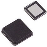
ICGOO电子元器件商城为您提供AD5405YCPZ由Analog设计生产,在icgoo商城现货销售,并且可以通过原厂、代理商等渠道进行代购。 AD5405YCPZ价格参考¥58.46-¥83.36。AnalogAD5405YCPZ封装/规格:数据采集 - 数模转换器, 12 位 数模转换器 2 40-LFCSP(6x6)。您可以下载AD5405YCPZ参考资料、Datasheet数据手册功能说明书,资料中有AD5405YCPZ 详细功能的应用电路图电压和使用方法及教程。
AD5405YCPZ是由Analog Devices Inc.(亚德诺半导体公司)生产的一款12位、四通道电压输出数模转换器(DAC),广泛应用于数据采集系统中。该器件具有低功耗、高精度和小封装的特点,适用于多种工业和消费类应用场景。

 应用场景:

1. 工业自动化与控制:
   AD5405YCPZ在工业自动化领域中用于精确控制各种模拟信号,例如调节电机速度、阀门开度或传感器反馈信号。其多通道设计允许同时控制多个设备或参数,提高了系统的集成度和效率。此外,其低功耗特性使其适合长时间运行的工业环境。

2. 测试与测量设备:
   在精密测试仪器中,如示波器、信号发生器等,AD5405YCPZ可以提供稳定且准确的电压输出,用于生成测试信号或校准其他设备。其12位分辨率确保了输出信号的高精度,满足高端测试设备的需求。

3. 通信系统:
   通信设备中常需要对模拟信号进行精确控制,AD5405YCPZ可以用于调整发射功率、接收增益等关键参数。其快速响应时间和低噪声性能使得它在无线通信基站、卫星通信等领域表现出色。

4. 医疗设备:
   医疗仪器如心电图机、超声波设备等对信号的精确性和稳定性要求极高。AD5405YCPZ能够为这些设备提供可靠的模拟信号输出,帮助实现更精准的诊断和治疗功能。其紧凑的封装也便于集成到便携式医疗设备中。

5. 音频处理:
   在音频设备中,AD5405YCPZ可用于生成高质量的音频信号,例如合成器、音效处理器等。其多通道特性支持立体声或多声道音频输出,而低噪声设计则保证了音频质量。

6. 消费电子:
   某些高端消费电子产品,如智能家居控制器、可穿戴设备等,也需要精确的模拟信号控制。AD5405YCPZ的小尺寸和低功耗特性使其成为这些应用的理想选择。

总之,AD5405YCPZ凭借其高性能和灵活性,在多个领域提供了可靠的数模转换解决方案,满足了不同应用场景对精度、功耗和集成度的要求。
| 参数 | 数值 |
| 产品目录 | 集成电路 (IC)半导体 |
| 描述 | IC DAC DUAL 12BIT MULT 40-LFCSP数模转换器- DAC Dual 12-bit Parallel IF IC |
| DevelopmentKit | EVAL-AD5405EBZ |
| 产品分类 | |
| 品牌 | Analog Devices Inc |
| 产品手册 | |
| 产品图片 |
|
| rohs | 符合RoHS无铅 / 符合限制有害物质指令(RoHS)规范要求 |
| 产品系列 | 数据转换器IC,数模转换器- DAC,Analog Devices AD5405YCPZ- |
| 数据手册 | |
| 产品型号 | AD5405YCPZ |
| PCN组件/产地 | |
| 产品培训模块 | http://www.digikey.cn/PTM/IndividualPTM.page?site=cn&lang=zhs&ptm=19145http://www.digikey.cn/PTM/IndividualPTM.page?site=cn&lang=zhs&ptm=18614http://www.digikey.cn/PTM/IndividualPTM.page?site=cn&lang=zhs&ptm=26125http://www.digikey.cn/PTM/IndividualPTM.page?site=cn&lang=zhs&ptm=26140http://www.digikey.cn/PTM/IndividualPTM.page?site=cn&lang=zhs&ptm=26150http://www.digikey.cn/PTM/IndividualPTM.page?site=cn&lang=zhs&ptm=26147 |
| 产品目录页面 | |
| 产品种类 | 数模转换器- DAC |
| 位数 | 12 |
| 供应商器件封装 | 40-LFCSP-VQ(6x6) |
| 分辨率 | 12 bit |
| 包装 | 托盘 |
| 商标 | Analog Devices |
| 安装类型 | 表面贴装 |
| 安装风格 | SMD/SMT |
| 封装 | Tray |
| 封装/外壳 | 40-VFQFN 裸露焊盘,CSP |
| 封装/箱体 | LFCSP-40 |
| 工作温度 | -40°C ~ 125°C |
| 工厂包装数量 | 490 |
| 建立时间 | 80ns |
| 接口类型 | Parallel |
| 数据接口 | 并联 |
| 最大功率耗散 | 50 uW |
| 最大工作温度 | + 125 C |
| 最小工作温度 | - 40 C |
| 标准包装 | 1 |
| 电压参考 | External |
| 电压源 | 单电源 |
| 电源电压-最大 | 5.5 V |
| 电源电压-最小 | 2.5 V |
| 积分非线性 | +/- 1 LSB |
| 稳定时间 | 80 ns |
| 系列 | AD5405 |
| 结构 | R-2R |
| 转换器数 | 2 |
| 转换器数量 | 2 |
| 输出数和类型 | 4 电流 |
| 输出类型 | Current |
| 配用 | /product-detail/zh/EVAL-AD5405EB/EVAL-AD5405EB-ND/699395 |
| 采样比 | 21.3 MSPs |
| 采样率(每秒) | 21.3M |


- 商务部:美国ITC正式对集成电路等产品启动337调查
- 曝三星4nm工艺存在良率问题 高通将骁龙8 Gen1或转产台积电
- 太阳诱电将投资9.5亿元在常州建新厂生产MLCC 预计2023年完工
- 英特尔发布欧洲新工厂建设计划 深化IDM 2.0 战略
- 台积电先进制程称霸业界 有大客户加持明年业绩稳了
- 达到5530亿美元!SIA预计今年全球半导体销售额将创下新高
- 英特尔拟将自动驾驶子公司Mobileye上市 估值或超500亿美元
- 三星加码芯片和SET,合并消费电子和移动部门,撤换高东真等 CEO
- 三星电子宣布重大人事变动 还合并消费电子和移动部门
- 海关总署:前11个月进口集成电路产品价值2.52万亿元 增长14.8%


PDF Datasheet 数据手册内容提取
Dual 12-Bit, High Bandwidth, Multiplying DAC with 4-Quadrant Resistors and Parallel Interface Data Sheet AD5405 FEATURES GENERAL DESCRIPTION 10 MHz multiplying bandwidth The AD54051 is a CMOS, 12-bit, dual-channel, current output On-chip 4-quadrant resistors allow flexible output ranges digital-to-analog converter (DAC). This device operates from a INL of ±1 LSB 2.5 V to 5.5 V power supply, making it suited to battery-powered 40-lead LFCSP package and other applications. 2.5 V to 5.5 V supply operation Because of manufacturing with a CMOS submicron process, the ±10 V reference input device offers excellent 4-quadrant multiplication characteristics, 21.3 MSPS update rate with large signal multiplying bandwidths of up to 10 MHz. Extended temperature range: −40°C to +125°C 4-quadrant multiplication The applied external reference input voltage (VREF) determines Power-on reset the full-scale output current. An integrated feedback resistor (RFB) 0.5 µA typical current consumption provides temperature tracking and full-scale voltage output when Guaranteed monotonic combined with an external I to V precision amplifier. This device Readback function also contains the 4-quadrant resistors necessary for bipolar operation and other configuration modes. APPLICATIONS This DAC uses data readback, allowing the user to read the Portable battery-powered applications contents of the DAC register via the DB pins. On power-up, the Waveform generators internal register and latches fill with 0s, and the DAC outputs Analog processing are at zero scale. Instrumentation applications Programmable amplifiers and attenuators The AD5405 has a 6 mm × 6 mm, 40-lead LFCSP package. Digitally controlled calibration 1 U.S. Patent Number 5,689,257. Programmable filters and oscillators Composite video Ultrasound Gain, offset, and voltage trimming FUNCTIONAL BLOCK DIAGRAM R3A R2_3A R2A VREFA R1A R3 R2 AD5405 2R 2R R1 RFB 2R 2R VDD RFBA DATA INPUTS DB0 INPUT LATCH 12-BIT IOUT1A DB11 BUFFER R-2R DAC A IOUT2A DACA/B CS CONTROL LOGIC R/W 12-BIT IOUT1B LATCH R-2R DAC B LDAC IOUT2B GND POWER-ON R1 RFB RFBB RESET R3 R2 2R 2R CLR R3B 2RR2_3B2RR2B VREFB R1B 04463-001 Figure 1. Rev. D Document Feedback Information furnished by Analog Devices is believed to be accurate and reliable. However, no responsibility is assumed by Analog Devices for its use, nor for any infringements of patents or other One Technology Way, P.O. Box 9106, Norwood, MA 02062-9106, U.S.A. rights of third parties that may result from its use. Specifications subject to change without notice. No license is granted by implication or otherwise under any patent or patent rights of Analog Devices. Tel: 781.329.4700 ©2004–2018 Analog Devices, Inc. All rights reserved. Trademarks and registered trademarks are the property of their respective owners. Technical Support www.analog.com
AD5405 Data Sheet TABLE OF CONTENTS Features .............................................................................................. 1 Circuit Operation ....................................................................... 14 Applications ....................................................................................... 1 Single-Supply Applications ....................................................... 15 General Description ......................................................................... 1 Adding Gain ................................................................................ 15 Functional Block Diagram .............................................................. 1 Divider or Programmable Gain Element ................................ 16 Revision History ............................................................................... 2 Reference Selection .................................................................... 16 Specifications ..................................................................................... 3 Amplifier Selection .................................................................... 16 Timing Characteristics ................................................................ 5 Parallel Interface ......................................................................... 18 Absolute Maximum Ratings ............................................................ 6 Microprocessor Interfacing ....................................................... 18 ESD Caution .................................................................................. 6 PCB Layout and Power Supply Decoupling ........................... 19 Pin Configuration and Function Descriptions ............................. 7 Overview of the AD5424 to AD5547 Devices ............................ 22 Typical Performance Characteristics ............................................. 8 Outline Dimensions ....................................................................... 23 Terminology .................................................................................... 13 Ordering Guide .......................................................................... 23 General Description ....................................................................... 14 DAC Section ................................................................................ 14 REVISION HISTORY 7/2018—Rev. C to Rev. D 7/2005—Rev. 0 to Rev. A Changes to Pin 2 and Pin 3, Mnemonic Column, Table 4 .......... 7 Changed Pin DAC A/B to DAC A/B ............................... Universal Changes to Features List ................................................................... 1 1/2016—Rev. B to Rev. C Changes to Specifications ................................................................. 3 Deleted Positive Output Voltage Section and Figure 35............ 15 Changes to Timing Characteristics ................................................. 5 Changes to Adding Gain Section ................................................. 15 Change to Absolute Maximum Ratings ......................................... 6 Changes to ADSP-21xx Processors to AD5405 Interface Section Change to Figure 7 and Figure 8 ..................................................... 8 Title, ADSP-BF504 to ADSP-BF592 Device Family to AD5405 Change to Figure 12 .......................................................................... 9 Interface Section Title, and Figure 39 Caption ........................... 19 Change to Figure 26 Through Figure 28 ..................................... 11 Deleted Evaluation Board for the DACs Section and Power Changes to General Description Section .................................... 14 Supplies for the Evaluation Board Section .................................. 19 Change to Figure 31 ....................................................................... 14 Changes to Table 10 ........................................................................ 22 Changes to Table 5 Through Table 10 ......................................... 14 Updated Outline Dimensions ....................................................... 23 Changes to Figure 34 and Figure 35 ............................................ 15 Changes to Ordering Guide .......................................................... 23 Changes to Figure 36 and Figure 37 ............................................ 16 Changes to Microprocessor Interfacing Section ........................ 18 12/2009—Rev. A to Rev. B Added Figure 38 Through Figure 40 ........................................... 18 Changes to Figure 1 .......................................................................... 1 Change to Power Supplies for the Evaluation Board Section ... 19 Changes to Table 2 and Figure 2 ..................................................... 5 Updated Outline Dimensions ....................................................... 23 Changes to Table 4 and Figure 4 ..................................................... 7 Changes to Ordering Guide .......................................................... 23 Updated Outline Dimensions ....................................................... 23 Changes to Ordering Guide .......................................................... 23 7/2004—Revision 0: Initial Version Rev. D | Page 2 of 24
Data Sheet AD5405 SPECIFICATIONS V = 2.5 V to 5.5 V, V = 10 V, I 2 = 0 V. Temperature range for Y version: −40°C to +125°C. All specifications T to T , unless DD REF OUT MIN MAX otherwise noted. DC performance is measured with OP177, and ac performance is measured with AD8038, unless otherwise noted. Table 1.1 Parameter Min Typ Max Unit Test Conditions/Comments STATIC PERFORMANCE Resolution 12 Bits Relative Accuracy ±1 LSB Differential Nonlinearity −1/+2 LSB Guaranteed monotonic Gain Error ±25 mV Gain Error Temperature Coefficient ±5 ppm FSR/°C Bipolar Zero-Code Error ±25 mV Output Leakage Current ±1 nA Data = 0x0000, T = 25°C, I 1 A OUT ±15 nA Data = 0x0000, T = −40°C to +125°C, I 1 A OUT REFERENCE INPUT Reference Input Range ±10 V V A, V B Input Resistance 8 10 13 kΩ Input resistance TC = −50 ppm/°C REF REF V A to V B Input Resistance 1.6 2.5 % Typ = 25°C, max = 125°C REF REF Mismatch R1, R Resistance 17 20 25 kΩ Input resistance TC = −50 ppm/°C FB R2, R3 Resistance 17 20 25 kΩ Input resistance TC = −50 ppm/°C R2 to R3 Resistance Mismatch 0.06 0.18 % Typ = 25°C, max = 125°C Input Capacitance Code 0 3.5 pF Code 4095 3.5 pF DIGITAL INPUTS/OUTPUT Input High Voltage, V 1.7 V V = 3.6 V to 5.5 V IH DD 1.7 V V = 2.5 V to 3.6 V DD Input Low Voltage, V 0.8 V V = 2.7 V to 5.5 V IL DD 0.7 V V = 2.5 V to 2.7 V DD Output High Voltage, V V − 1 V V = 4.5 V to 5.5 V, I = 200 µA OH DD DD SOURCE V − 0.5 V V = 2.5 V to 3.6 V, I = 200 µA DD DD SOURCE Output Low Voltage, V 0.4 V V = 4.5 V to 5.5 V, I = 200 µA OL DD SINK 0.4 V V = 2.5 V to 3.6 V, I = 200 µA DD SINK Input Leakage Current, I 1 µA IL Input Capacitance 4 10 pF DYNAMIC PERFORMANCE Reference Multiplying BW 10 MHz V = ±3.5 V p-p, DAC loaded all 1s REF Output Voltage Settling Time R = 100 Ω, C = 15 pF, V = 10 V LOAD LOAD REF DAC latch alternately loaded with 0s and 1s Measured to ±1 mV of FS 80 120 ns Measured to ±4 mV of FS 35 70 ns Measured to ±16 mV of FS 30 60 ns Digital Delay 20 40 ns Interface time delay 10% to 90% Settling Time 15 30 ns Rise and fall times Digital-to-Analog Glitch Impulse 3 nV-sec 1 LSB change around major carry, V = 0 V REF Multiplying Feedthrough Error DAC latch loaded with all 0s, V = ±3.5 V REF 70 dB 1 MHz 48 dB 10 MHz Output Capacitance 12 17 pF DAC latches loaded with all 0s 25 30 pF DAC latches loaded with all 1s Rev. D | Page 3 of 24
AD5405 Data Sheet Parameter Min Typ Max Unit Test Conditions/Comments Digital Feedthrough 1 nV-sec Feedthrough to DAC output with CS high and alternate loading of all 0s and all 1s Output Noise Spectral Density 25 nV/√Hz At 1 kHz Analog THD 81 dB V = 3. 5 V p-p, all 1s loaded, f = 1 kHz REF Digital THD Clock = 10 MHz, V = 3.5 V REF 100 kHz f 61 dB OUT 50 kHz f 66 dB OUT SFDR Performance (Wideband) V = 3.5 V REF Clock = 10 MHz 500 kHz f 55 dB OUT 100 kHz f 63 dB OUT 50 kHz f 65 dB OUT Clock = 25 MHz 500 kHz f 50 dB OUT 100 kHz f 60 dB OUT 50 kHz f 62 dB OUT SFDR Performance (Narrow Band) V = 3.5 V REF Clock = 10 MHz 500 kHz f 73 dB OUT 100 kHz f 80 dB OUT 50 kHz f 87 dB OUT Clock = 25 MHz 500 kHz f 70 dB OUT 100 kHz f 75 dB OUT 50 kHz f 80 dB OUT Intermodulation Distortion V = 3.5 V REF f = 40 kHz, f = 50 kHz 72 dB Clock = 10 MHz 1 2 f = 40 kHz, f = 50 kHz 65 dB Clock = 25 MHz 1 2 POWER REQUIREMENTS Power Supply Range 2.5 5.5 V I 0.7 µA T = 25°C, logic inputs = 0 V or V DD A DD 0.5 10 µA T = −40°C to +125°C, logic inputs = 0 V or V A DD Power Supply Sensitivity 0.001 %/% ∆V = ±5% DD 1 Guaranteed by design and characterization, not subject to production test. Rev. D | Page 4 of 24
Data Sheet AD5405 TIMING CHARACTERISTICS All input signals are specified with tr = tf = 1 ns (10% to 90% of V ) and timed from a voltage level of (V + V )/2. V = 2.5 V to 5.5 V, DD IL IH DD V = 10 V, I 2 = 0 V, temperature range for Y version: −40°C to +125°C. All specifications T to T , unless otherwise noted. REF OUT MIN MAX Table 2.1 Parameter Limit at T , T Unit Test Conditions/Comments MIN MAX Write Mode t1 0 ns min R/W to CS setup time t2 0 ns min R/W to CS hold time t3 10 ns min CS low time t 10 ns min Address setup time 4 t 0 ns min Address hold time 5 t 6 ns min Data setup time 6 t 0 ns min Data hold time 7 t8 5 ns min R/W high to CS low t9 7 ns min CS min high time t14 10 ns typ CS rising to LDAC falling time t15 12 ns typ LDAC pulse width t16 10 ns typ CS rising to LDAC rising time t17 10 ns typ LDAC falling to CS rising time Data Readback Mode t 0 ns typ Address setup time 10 t 0 ns typ Address hold time 11 t 5 ns typ Data access time 12 35 ns max t 5 ns typ Bus relinquish time 13 10 ns max Update Rate 21.3 MSPS Consists of CS min high time, CS low time, and output voltage settling time 1 Guaranteed by design and characterization, not subject to production test. t1 t2 t8 t2 R/W t9 CS t3 t4 t5 t10 t11 DACA/DACB t6 t7 t12 t13 DATA DATA VALID DATA VALID t14 t15 LDAC1 t17 t16 LDAC2 12ASYSNYNCCHHRROONNOOUUS SL DLDAACC U UPDPDAATET EM MOODDE.E. 04463-002 Figure 2. Timing Diagram 200µA IOL TO VOH (MIN)+ VOL (MAX) OUTPUT PIN CL 2 50pF 200µA IOH 04463-003 Figure 3. Load Circuit for Data Timing Specifications Rev. D | Page 5 of 24
AD5405 Data Sheet ABSOLUTE MAXIMUM RATINGS Transient currents of up to 100 mA do not cause SCR latch-up. Stresses at or above those listed under Absolute Maximum T = 25°C, unless otherwise noted. A Ratings may cause permanent damage to the product. This is a stress rating only; functional operation of the product at these Table 3. or any other conditions above those indicated in the operational Parameter Rating section of this specification is not implied. Operation beyond V to GND −0.3 V to +7 V DD the maximum operating conditions for extended periods may V A, V B, R A, R B to GND −12 V to +12 V REF REF FB FB affect product reliability. I 1, I 2 to GND −0.3 V to +7 V OUT OUT Logic Inputs and Output1 −0.3 V to V + 0.3 V ESD CAUTION DD Operating Temperature Range Automotive (Y Version) −40°C to +125°C Storage Temperature Range −65°C to +150°C Junction Temperature 150°C 40-lead LFCSP, θ Thermal Impedance 30°C/W JA Lead Temperature, Soldering (10 sec) 300°C Infrared (IR) Reflow, Peak Temperature 235°C (<20 sec) 1 Overvoltages at DBx, LDAC, CS, and R/W are clamped by internal diodes. Rev. D | Page 6 of 24
Data Sheet AD5405 PIN CONFIGURATION AND FUNCTION DESCRIPTIONS AA BB A21 12B 0 RFB9 IOUT8 IOUT7 NIC6 NIC5 NIC4 NIC3 IOUT2 IOUT1 RFB 4333333333 R1A 1 30 R1B R2A 2 29 R2B R2_3A 3 28 R2_3B R3A 4 27 R3B VREFA 5 AD5405 26VREFB DGND 6 TOP VIEW 25VDD LDAC 7 (Not to Scale) 24 CLR DACA/B 8 23 R/W NIC 9 22 CS DB1110 21 DB0 11121314151617181920 DB10DB9 DB8 DB7 DB6 DB5 DB4 DB3 DB2 DB1 N12..O NETIXCEPS =O NSOETD IPNATDE RMNUASLTL YB EC OCNONNENCETCETDE.DTO GROUND. 04463-004 Figure 4. Pin Configuration Table 4. Pin Function Descriptions Pin No. Mnemonic Description 1 to 4 R1A, R2A, DAC A 4-Quadrant Resistors. Allow a number of configuration modes, including bipolar operation with R2_3A, R3A minimum of external components. 5, 26 V A, V B DAC Reference Voltage Input Terminals. REF REF 6 DGND Digital Ground Pin. 7 LDAC Load DAC Input. Allows asynchronous or synchronous updates to the DAC output. The DAC is asynchronously updated when this signal goes low. Alternatively, if this line is held permanently low, an automatic or synchronous update mode is selected whereby the DAC is updated on the rising edge of CS. 8 DAC A/B Selects DAC A or B. Low selects DAC A, and high selects DAC B. 9, 34 to 37 NIC Not internally connected. 10 to 21 DB11 to DB0 Parallel Data Bits 11 through 0. 22 CS Chip Select Input. Active low. Used in conjunction with R/W to load parallel data to the input latch or to read data from the DAC register. Edge sensitive; when pulled high, the DAC data is latched. 23 R/W Read/Write. When low, used in conjunction with CS to load parallel data. When high, used in conjunction with CS to read back contents of DAC register. 24 CLR Active Low Control Input. Clears DAC output and input and DAC registers. 25 V Positive Power Supply Input. These devices can be operated from a supply of 2.5 V to 5.5 V. DD 27 to 30 R3B, R2_3B, DAC B 4-Quadrant Resistors. Allow a number of configuration modes, including bipolar operation with a R2B, R1B minimum of external components. 31, 40 R B, R A External Amplifier Output. FB FB 32 I 2B DAC A Analog Ground. This pin typically ties to the analog ground of the system, but can be biased to OUT achieve single-supply operation. 33 I 1B DAC B Current Outputs. OUT 38 I 1A DAC A Current Outputs. OUT 39 I 2A DAC A Analog Ground. This pin typically ties to the analog ground of the system, but can be biased to OUT achieve single-supply operation. EPAD Exposed pad must be connected to ground. Rev. D | Page 7 of 24
AD5405 Data Sheet TYPICAL PERFORMANCE CHARACTERISTICS 1.0 –0.40 0.8 TVAR E=F 2=5 °1C0V TVAD D= =2 55°VC 0.6 VDD = 5V –0.45 0.4 –0.50 B) 0.2 B) S S NL (L 0 NL (L–0.55 I –0.2 D –0.60 –0.4 MIN DNL –0.6 –0.65 –0.8 –1.00 500 1000 1500 C2O0D00E 2500 3000 3500 4000 04463-030 –0.702 3 4 REF5ERENC6E VOLTA7GE 8 9 10 04463-033 Figure 5. Integral Nonlinearity (INL) vs. Code (12-Bit DAC) Figure 8. Differential Nonlinearity (DNL) vs. Reference Voltage 1.0 5 00..68 TVVARD ED=F = 2= 55 °1VC0V 34 VDD = 5V 0.4 2 B) 0.2 mV) 1 DNL (LS –0.20 ERROR ( –10 VDD = 2.5V –0.4 –2 –0.6 –3 –0.8 –4 VREF = 10V –1.0 –5 0 500 1000 1500 C2O0D00E 2500 3000 3500 4000 04463-031 –60 –40 –20 0 TE2M0PERA40TURE6 0(°C) 80 100 120 140 04463-034 Figure 6. DNL vs. Code (12-Bit DAC) Figure 9. Gain Error vs. Temperature 0.6 8 TA = 25°C 0.5 7 0.4 6 MAX INL 0.3 SB) 0.2 T (mA) 5 VDD = 5V INL (L 0.1 TVAD D= =2 55°VC CURREN 34 0 MIN INL 2 –0.1 VDD = 3V –0.2 1 VDD = 2.5V –0.32 3 4 REF5ERENC6E VOLTA7GE 8 9 10 04463-032 00 0.5 1.0 1.5INP2U.0T VO2L.5TAG3E. 0(V) 3.5 4.0 4.5 5.0 04463-013 Figure 7. INL vs. Reference Voltage Figure 10. Supply Current vs. Logic Input Voltage Rev. D | Page 8 of 24
Data Sheet AD5405 1.6 60 TLAO A= D2I5N°GC DABLL1 1ON 1.4 –6 ZS TO FS DB10 –12 DB9 –18 1.2 DB8 –24 E (nA) 01..80 IOUT1 VDD = 5V GAIN (dB) ––––43432086 DDDDBBBB7654 G DB3 1 LEAKAOUT 00..46 IOUT1 VDD = 3V –––––6567764028 DDDBBB201 TA = 25°C I –84 VDD = 5V 0.2 –90 VREF =±3.5V 0–40 –20 0 TE20MPERA4T0URE (6°C0) 80 100 120 04463-036 –1–09261 10 10A0LL O1FFkRFEQU1E0NkCY (H10z0)k 1MACMCPOM =1P 0AM=D18.80p13F080M 04463-014 Figure 11. IOUT1 Leakage Current vs. Temperature Figure 14. Reference Multiplying Bandwidth vs. Frequency and Code 0.50 0.2 0.45 VDD = 5V 0.40 0 0.35 A) ALL 0s µENT ( 00..2350 ALL 1s N (dB) –0.2 URR 0.20 VDD = 2.5V GAI –0.4 C 0.15 ALL 1s ALL 0s TA = 25°C 0.10 –0.6 VDD = 5V VREF =±3.5V 0.05 CCOMP = 1.8pF AMP = AD8038 0–60 –40 –20 0 TE2M0PERA40TURE6 0(°C) 80 100 120 140 04463-037 –0.81 10 100 F1kREQU1E0NkCY (H10z0)k 1M 10M 100M 04463-029 Figure 12. Supply Current vs. Temperature Figure 15. Reference Multiplying Bandwidth—All 1s Loaded 14 3 LTOA A= D2I5N°GC ZS TO FS TVAD D= =2 55°VC 12 VDD = 5V 0 10 A) 8 dB) I (mDD 6 VDD = 3V GAIN ( –3 4 –6 VREF =±2V, AD8038 CC 1.47pF VDD = 2.5V VREF =±2V, AD8038 CC 1pF VREF =±0.15V, AD8038 CC 1pF 2 VREF =±0.15V, AD8038 CC 1.47pF VREF =±3.51V, AD8038 CC 1.8pF 01 10 100 F1kREQU1E0NkCY (H10z0)k 1M 10M 100M 04463-038 –910k 100k FREQUE1MNCY (Hz) 10M 100M04463-015 Figure 13. Supply Current vs. Update Rate Figure 16. Reference Multiplying Bandwidth vs. Frequency and Compensation Capacitor Rev. D | Page 9 of 24
AD5405 Data Sheet 0.045 –60 0x7FF TO 0x800 TA = 25°C TA = 25°C 0.040 VREF = 0V VDD = 3V 0.035 VDD = 5V ACMCOPM =P A=D 18.80p3F8 –65 VREF = 3.5V p-p V) 0.030 E ( 0.025 –70 UT VOLTAG 00..001250 VDD = 3V 0x800 TO 0x7FF HD + N (dB) –75 OUTP 00..000150 VDD = 3V T –80 0 –85 –0.005 VDD = 5V –0.0100 20 40 60 80TIM1E0 0(ns)120 140 160 180 200 04463-039 –901 10 100FREQUE1NkCY (Hz)10k 100k 1M 04463-041 Figure 17. Midscale Transition, VREF = 0 V Figure 20. THD and Noise vs. Frequency –1.68 100 0x7FF TO 0x800 TA = 25°C –1.69 VREF = 3.5V MCLK = 1MHz –1.70 VDD = 5V ACMCOPM =P A=D 18.80p3F8 80 V) E ( –1.71 AG B) 60 MCLK = 200kHz VOLT –1.72 VDD = 3V DR (d MCLK = 0.5MHz T –1.73 F U S 40 UTP –1.74 VDD = 5V O VDD = 3V –1.75 20 –1.76 0x800 TO 0x7FF TVAARM E=PF 2==5 A°3C.D58V038 –1.77 0 0 20 40 60 80TIM1E0 0(ns)120 140 160 180 200 04463-040 0 20 40 60 80fOU1T 0(0kHz)120 140 160 180 200 04463-027 Figure 18. Midscale Transition, VREF = 3.5 V Figure 21. Wideband SFDR vs. fOUT Frequency 20 TA = 25°C 90 VDD = 3V 80 0 AMP = AD8038 MCLK = 5MHz 70 MCLK = 10MHz –20 60 dB) –40 dB) 50 R ( FULL SCALE R ( PSR –60 ZERO SCALE SFD 40 MCLK = 25MHz 30 –80 20 –100 10 VTAR E=F 2=5 °3C.5V AMP = AD8038 –1201 10 100 FRE1QkUENC1Y0 (kHz) 100k 1M 10M04463-026 00 100 200 300 400fOU5T 0(0kHz)600 700 800 900 1000 04463-028 Figure 19. Power Supply Rejection Ratio vs. Frequency Figure 22. Wideband SFDR vs. fOUT Frequency Rev. D | Page 10 of 24
Data Sheet AD5405 0 0 TA = 25°C TA� = 25°C –10 VADMDP = = 5 AVD8038 –10 VADMDP = = 3 AVD8038 65k CODES –20 65k CODES –20 –30 –30 B) –40 d–40 SFDR (–50 DR (dB)––5600 F –60 S –70 –70 –80 –80 –90 –900 2 4FREQUEN6CY (MHz)8 10 12 04463-018 –100250 300 350 400 FR45E0QUE5N00CY (5k5H0z) 600 650 700 750 04463-021 Figure 23. Wideband SFDR, fOUT = 100 kHz, Clock = 25 MHz Figure 26. Narrow-Band Spectral Response, fOUT = 500 kHz, Clock = 25 MHz 0 20 TA� = 25°C TA� = 25°C –10 VDD = 5V VDD = 3V AMP = AD8038 0 AMP = AD8038 –20 65k CODES 65k CODES –30 –20 B)–40 B)–40 d d R (–50 R ( D D SF–60 SF–60 –70 –80 –80 –100 –90 –1000 0.5 1.0 1.5 FR2E.0QUE2N.5CY (M3.H0z) 3.5 4.0 4.5 5.0 04463-019 –12050 60 70 80 FR9E0QUE1N00CY (1k1H0z) 120 130 140 150 04463-022 Figure 24. Wideband SFDR, fOUT = 500 kHz, Clock = 10 MHz Figure 27. Narrow-Band SFDR, fOUT = 100 kHz, Clock = 25 MHz 0 0 TA = 25°C TA� = 25°C –10 AVDMDP = = 5 AVD8038 –10 VADMDP = = 3 AVD8038 –20 65k CODES –20 65k CODES –30 –30 B) –40 d–40 R ( B)–50 D d F–50 ( S –60 –60 –70 –70 –80 –80 –90 –900 0.5 1.0 1.5 FR2E.0QUE2N.5CY (M3.H0z) 3.5 4.0 4.5 5.0 04463-020 –10070 75 80 85 FR9E0QUE9N5CY (1k0H0z) 105 110 115 120 04463-023 Figure 25. Wideband SFDR, fOUT = 50 kHz, Clock = 10 MHz Figure 28. Narrow-Band IMD, fOUT = 90 kHz, 100 kHz, Clock = 10 MHz Rev. D | Page 11 of 24
AD5405 Data Sheet 0 300 TA� = 25°C TA = 25°C –10 VDD = 5V ZERO SCALE LOADED TO DAC AMP = AD8038 AMP = AD8038 250 MIDSCALE LOADED TO DAC –20 65k CODES FULL SCALE LOADED TO DAC –30 Hz) V/ 200 –40 E (n dB)–50 OIS 150 ( N –60 UT P T 100 –70 U O –80 50 –90 –1000 50 100 1F5R0EQUE2N00CY (kH25z0) 300 350 400 04463-024 0100 1kFREQUENCY (Hz)10k 100k04463-025 Figure 29. Wideband IMD, fOUT = 90 kHz, 100 kHz, Clock = 25 MHz Figure 30. Output Noise Spectral Density Rev. D | Page 12 of 24
Data Sheet AD5405 TERMINOLOGY Relative Accuracy (Endpoint Nonlinearity) Multiplying Feedthrough Error A measure of the maximum deviation from a straight line The error due to capacitive feedthrough from the DAC passing through the endpoints of the DAC transfer function. It reference input to the DAC I 1 terminal when all 0s are OUT is measured after adjusting for zero and full scale and is normally loaded to the DAC. expressed in LSBs or as a percentage of the full-scale reading. Digital Crosstalk Differential Nonlinearity The glitch impulse transferred to the outputs of a DAC in The difference in the measured change and the ideal 1 LSB change response to a full-scale code change (all 0s to all 1s, or vice between two adjacent codes. A specified differential nonlinearity of versa) in the input register of another DAC. It is expressed in −1 LSB maximum over the operating temperature range ensures nV-sec. monotonicity. Analog Crosstalk Gain Error (Full-Scale Error) The glitch impulse transferred to the output of one DAC due to A measure of the output error between an ideal DAC and the a change in the output of another DAC. It is measured by actual device output. For this DAC, ideal maximum output is loading one of the input registers with a full-scale code change V − 1 LSB. The gain error of the DAC is adjustable to zero (all 0s to all 1s, or vice versa) while keeping LDAC high and REF with an external resistance. then pulsing LDAC low and monitoring the output of the DAC whose digital code has not changed. The area of the glitch is Output Leakage Current expressed in nV-sec. The current that flows into the DAC ladder switches when they are turned off. For the I 1 terminal, it can be measured by Channel to Channel Isolation OUT loading all 0s to the DAC and measuring the I 1 current. The portion of input signal from a DAC reference input that OUT Minimum current flows into the I 2 line when the DAC is appears at the output of the other DAC. It is expressed in decibels. OUT loaded with all 1s. Total Harmonic Distortion (THD) Output Capacitance The DAC is driven by an ac reference. The ratio of the rms sum Capacitance from I 1 or I 2 to AGND. of the harmonics of the DAC output to the fundamental value is OUT OUT the THD. Usually only the lower-order harmonics are included, Output Current Settling Time such as the second to the fifth harmonics. The amount of time for the output to settle to a specified level for a full-scale input change. For this device, it is specified with V 2+V 2+V 2+V 2 a 100 Ω resistor to ground. THD=20log 2 3 4 5 V 1 Digital-to-Analog Glitch Impulse Intermodulation Distortion (IMD) The amount of charge injected from the digital inputs to the The DAC is driven by two combined sine wave references analog output when the inputs change state. This is typically of frequencies fa and fb. Distortion products are produced specified as the area of the glitch in either pA-sec or nV-sec, at sum and difference frequencies of mfa ± nfb, where m, n = 0, depending on whether the glitch is measured as a current or 1, 2, 3 ... Intermodulation terms are those for which m or n is voltage signal. not equal to 0. The second-order terms include (fa + fb) and Digital Feedthrough (fa − fb), and the third-order terms are (2fa + fb), (2fa − fb), When the device is not selected, high frequency logic activity (f + 2fa + 2fb), and (fa − 2fb). IMD is defined as on the device’s digital inputs is capacitively coupled through the (rmssumof thesumanddiff distortionproducts) device and produces noise on the IOUT pins and, subsequently, IMD=20log on the following circuitry. This noise is digital feedthrough. rmsamplitudeof the fundamental Compliance Voltage Range The maximum range of (output) terminal voltage for which the device provides the specified characteristics. Rev. D | Page 13 of 24
AD5405 Data Sheet GENERAL DESCRIPTION DAC SECTION When an output amplifier is connected in unipolar mode, the output voltage is given by The AD5405 is a 12-bit, dual-channel, current-output DAC consisting of a standard inverting R-2R ladder configuration. VOUT =−VREF×D 2n Figure 31 shows a simplified diagram for a single channel of the where: AD5405. The feedback resistor R A has a value of 2R. The value of FB D is the fractional representation, in the range of 0 to 4,095, of R is typically 10 kΩ (with a minimum of 8 kΩ and a maximum the digital word loaded to the DAC. of 13 kΩ). If I 1A and I 2A are kept at the same potential, a OUT OUT n is the resolution of the DAC. constant current flows into each ladder leg, regardless of digital With a fixed 10 V reference, the circuit shown in Figure 32 gives input code. Therefore, the input resistance presented at V A is REF a unipolar 0 V to −10 V output voltage swing. When V is an ac always constant. IN signal, the circuit performs 2-quadrant multiplication. R R R VREFA Table 5 shows the relationship between digital code and the 2R 2R 2R 2R 2R expected output voltage for unipolar operation. S1 S2 S3 S12 R RFB A IOUT1A Table 5. Unipolar Code IOUT2A Digital Input Analog Output (V) DACA NDDA TDAR ILVAETRCSHES 04463-005 11101010 10101010 10101010 −−VVREF ((42,,009458//44,,009966)) = −V /2 REF REF Figure 31. Simplified Ladder Configuration 0000 0000 0001 −V (1/4,096) REF Access is provided to the VREF, RFB, IOUT1, and IOUT2 terminals of 0000 0000 0000 −VREF (0/4,096) = 0 the DAC, making the device extremely versatile and allowing it to be configured for several operating modes, such as unipolar Bipolar Operation output, bipolar output, or single-supply mode. In some applications, it may be necessary to generate full CIRCUIT OPERATION 4-quadrant multiplying operation or a bipolar output swing. This can be easily accomplished by using another external Unipolar Mode amplifier, as shown in Figure 33. Using a single operational amplifier, this DAC can easily be configured to provide 2-quadrant multiplying operation or a VDD R1A R1 RFB unipolar output voltage swing, as shown in Figure 32. 2R 2R RFBA R2A VIN C1 VDD R1A R2_3A R2R2 12A-BDit5 D4A0C5 A IIOOUUTT21AA A1 R1 RFB R VOUT =–VIN TO +VIN 2R 2R RFBA R2R3 R2A C1 A1 R3A R2R2 AD5405 IOUT1A A1 VREFA GND AGND R2_3A 12-Bit DAC A IOUT2A AGND R VOUT = 0V TO–VIN AGND R3 NOTES R3A 2R 12.. ISCFI1 MA PI1LH AIASR SA EC H OCINGOFHMI GPSUEPNRESEAADTIT OAIOMNN PF LO(1IFRpI FED RTAO.C 2Bp.F) MAY BE REQUIRED 04463-007 AGND VREFA GND AGND Figure 33. Bipolar Operation (4-Quadrant Multiplication) When in bipolar mode, the output voltage is given by AGND N12..O SCTI1EM SPILHAARS EC OCNOFMIGPUENRSAATITOIONN F O(1Rp FD TAOC 2Bp.F) MAY BE REQUIRED 04463-006 VOUT =(VREF×D 2n−1)−VREF IF A1 IS A HIGH SPEED AMPLIFIER. where: Figure 32. Unipolar Operation D is the fractional representation, in the range of 0 to 4095, of the digital word loaded to the DAC. n is the number of bits. When V is an ac signal, the circuit performs 4-quadrant IN multiplication. Table 6 shows the relationship between the digital code and the expected output voltage for bipolar operation. Rev. D | Page 14 of 24
Data Sheet AD5405 Note that V is limited to low voltages because the switches in the Table 6. Bipolar Code IN DAC ladder no longer have the same source drain drive voltage. Digital Input Analog Output (V) As a result, their on resistance differs and degrades the integral 1111 1111 1111 +V (4,095/4,096) REF linearity of the DAC. Also, V must not go negative by more 1000 0000 0000 0 IN than 0.3 V, or an internal diode turns on, causing the device to 0000 0000 0001 −V (4,095/4,096) REF exceed the maximum ratings. In this type of application, the full 0000 0000 0000 −V (4,096/4,096) REF range of multiplying capability of the DAC is lost. Stability ADDING GAIN In the I-to-V configuration, the I of the DAC and the inverting In applications where the output voltage must be greater than V , OUT IN node of the operational amplifier must be connected as close as gain can be added with an additional external amplifier, or it can be possible, and proper printed circuit board (PCB) layout techniques achieved in a single stage. Consider the effect of temperature must be used. Because every code change corresponds to a step coefficients of the thin film resistors of the DAC. Simply placing function, gain peaking may occur if the operational amplifier has a resistor in series with the R resistor causes mismatches in the FB limited gain bandwidth product (GBP) and there is excessive temperature coefficients, resulting in larger gain temperature parasitic capacitance at the inverting node. This parasitic cap- coefficient errors. Instead, the circuit of Figure 35 shows the acitance introduces a pole into the open-loop response, which can recommended method for increasing the gain of the circuit. R1, cause ringing or instability in the closed-loop applications circuit. R2, and R3 can have similar temperature coefficients, but they need not match the temperature coefficients of the DAC. This An optional compensation capacitor, C1, can be added in parallel approach is recommended in circuits where gains of greater than with R A for stability, as shown in Figure 32 and Figure 33. Too FB 1 are required. Note that R R2//R3 and a gain error percentage small a value of C1 can produce ringing at the output, whereas FB of 100 × (R2//R3)/R must be taken into consideration. too large a value can adversely affect the settling time. C1 can be FB ≫ found empirically, but 1 pF to 2 pF is generally adequate for the VDD compensation. SINGLE-SUPPLY APPLICATIONS C1 VDD RFBA Voltage Switching Mode of Operation VIN R1 VREFA 12-BIT IOUT1A VOUT DAC IOUT2A Figure 34 shows the DAC operating in the voltage switching R3 GND mode. The reference voltage, V , is applied to the I 1A pin, IN OUT R2 GAIN = R2 + R3 IOUT2A is connected to AGND, and the output voltage is available at R2 the V A terminal. In this configuration, a positive reference NOTES R1 = R2R3 REF voopletaragtei orens uplotss sinib ale p. oTshiteiv oeu otuptuptu ftr voomlt atghee, mDAakCin igs svionlgtaleg-es uapt pal y 12..ISCFI1 MA PI1LH AIASR SA EC H OCINGOFHMI GPSUEPNRESEAADTIT OAIOMNN PF LO(1IFRpI FED RTAO.C 2Bp.F) MAY BE REQUIRED R2 + R3 04463-011 constant impedance (the DAC ladder resistance). Therefore, an Figure 35. Increasing Gain of Current Output DAC operational amplifier is necessary to buffer the output voltage. The reference input no longer sees a constant input impedance, but one that varies with code. Therefore, the voltage input must be driven from a low impedance source. VDD R1 R2 RFBA VDD VIN IOUT1A VOUT VREFA IOUT2A GND N12..OSCTI1EM PSILHAARS EC OCNOFMIGPUENRSAATITOIONN F O(1Rp FD TAOC 2Bp.F) MAY BE REQUIRED 04463-009 IF A1 IS A HIGH SPEED AMPLIFIER. Figure 34. Single-Supply Voltage-Switching Mode Rev. D | Page 15 of 24
AD5405 Data Sheet DIVIDER OR PROGRAMMABLE GAIN ELEMENT REFERENCE SELECTION Current steering DACs are very flexible and lend themselves to When selecting a reference for use with the AD5405 and other many applications. If this type of DAC is connected as the feedback devices in this series of current output DACs, pay attention to the element of an operational amplifier and R A is used as the output voltage temperature coefficient specification of the FB input resistor, as shown in Figure 36, the output voltage is reference. This parameter not only affects the full-scale error, inversely proportional to the digital input fraction, D. but also can affect the linearity (INL and DNL) performance. The reference temperature coefficient must be consistent with the For D = 1 − 2−n, the output voltage is system accuracy specifications. For example, an 8-bit system V =−V D=−V (1−2−n) required to hold its overall specification to within 1 LSB over the OUT IN IN temperature range 0°C to 50°C dictates that the maximum system VDD drift with temperature must be less than 78 ppm/°C. A 12-bit VIN system with the same temperature range to overall specification RFBA VDD within 2 LSBs requires a maximum drift of 10 ppm/°C. IOUT1A Choosing a precision reference with low output temperature IOUT2A VREFA coefficient minimizes this error source. Table 7 lists some GND references available from Analog Devices, Inc., that are suitable for use with this range of current output DACs. AMPLIFIER SELECTION VOUT The primary requirement for the current steering mode is an amplifier with low input bias currents and low input offset voltage. N1.O ATDEDSITIONAL PINS OMITTED FOR CLARITY. 04463-012 iBnepcuatu oseff soeft t vhoel ctaogdee o df eapne nopdeernatt oiountpalu at mrepslisiftiaenr cies mofu thlteip DlieAdC b, yt hthe e Figure 36. Current Steering DAC Used as a Divider or variable gain of the circuit. A change in this noise gain between Programmable Gain Element two adjacent digital fractions produces a step change in the output As D is reduced, the output voltage increases. For small values of voltage due to the amplifier’s input offset voltage. This output the digital fraction D, it is important to ensure that the amplifier voltage change is superimposed on the desired change in output does not saturate and that the required accuracy is met. For between the two codes and gives rise to a differential linearity example, an 8-bit DAC driven with the binary code 0x10 (0001 error, which, if large enough, could cause the DAC to be 0000)—that is, 16 decimal—in the circuit of Figure 36 can cause nonmonotonic. the output voltage to be 16 times V . However, if the DAC has a IN The input bias current of an operational amplifier also generates linearity specification of ±0.5 LSB, D can have a weight in the range an offset at the voltage output because of the bias current flowing of 15.5/256 to 16.5/256 so that the possible output voltage is in in the feedback resistor, R . Most operational amplifiers have input FB the range of 15.5 V to 16.5 V —an error of 3%, even though IN IN bias currents low enough to prevent significant errors in 12-bit the DAC itself has a maximum error of 0.2%. applications. DAC leakage current is also a potential error source in divider Common-mode rejection of the operational amplifier is circuits. The leakage current must be counterbalanced by an important in voltage switching circuits, because it produces a opposite current supplied from the operational amplifier through code dependent error at the voltage output of the circuit. Most the DAC. Because only a fraction, D, of the current into the operational amplifiers have adequate common-mode rejection V terminal is routed to the I 1 terminal, the output voltage REF OUT for use at 12-bit resolution. changes as follows: If the DAC switches are driven from true wideband, low Output Error Voltage Due to DAC Leakage = (Leakage × R)/D impedance sources (V and AGND), they settle quickly. IN where R is the DAC resistance at the V terminal. Consequently, the slew rate and settling time of a voltage-switching REF DAC circuit is determined largely by the output operational For a DAC leakage current of 10 nA, R = 10 kΩ, and a gain (that amplifier. To obtain minimum settling time in this configuration, is, 1/D) of 16, the error voltage is 1.6 mV. minimize capacitance at the V node (the voltage output node REF in this application) of the DAC. This is done by using low input capacitance buffer amplifiers and careful board design. Most single-supply circuits include ground as part of the analog signal range, which in turn requires an amplifier that can handle rail-to-rail signals. Analog Devices offers a wide range of single- supply amplifiers, as listed in Table 8 and Table 9. Rev. D | Page 16 of 24
Data Sheet AD5405 Table 7. Suitable Analog Devices Precision References Part No. Output Voltage (V) Initial Tolerance (%) Temp Drift (ppm/°C) I (mA) Output Noise (µV p-p) Package SS ADR01 10 0.05 3 1 20 SOIC-8 ADR01 10 0.05 9 1 20 TSOT-23, SC70 ADR02 5 0.06 3 1 10 SOIC-8 ADR02 5 0.06 9 1 10 TSOT-23, SC70 ADR03 2.5 0.10 3 1 6 SOIC-8 ADR03 2.5 0.10 9 1 6 TSOT-23, SC70 ADR06 3 0.10 3 1 10 SOIC-8 ADR06 3 0.10 9 1 10 TSOT-23, SC70 ADR431 2.5 0.04 3 0.8 3.5 SOIC-8 ADR435 5 0.04 3 0.8 8 SOIC-8 ADR391 2.5 0.16 9 0.12 5 TSOT-23 ADR395 5 0.10 9 0.12 8 TSOT-23 Table 8. Suitable Analog Devices Precision Operational Amplifiers 0.1 Hz to 10 Hz Part No. Supply Voltage (V) VOS (Max) (µV) IB (Max) (nA) Noise (µV p-p) Supply Current (µA) Package OP97 ±2 to ±20 25 0.1 0.5 600 SOIC-8 OP1177 ±2.5 to ±15 60 2 0.4 500 MSOP, SOIC-8 AD8551 2.7 to 5 5 0.05 1 975 MSOP, SOIC-8 AD8603 1.8 to 6 50 0.001 2.3 50 TSOT AD8628 2.7 to 6 5 0.1 0.5 850 TSOT, SOIC-8 Table 9. Suitable Analog Devices High Speed Operational Amplifiers Part No. Supply Voltage (V) BW at ACL (MHz) Slew Rate (V/µs) VOS (Max) (µV) I (Max) (nA) Package B AD8065 5 to 24 145 180 1,500 6,000 SOIC-8, SOT-23, MSOP AD8021 ±2.5 to ±12 490 120 1,000 10,500 SOIC-8, MSOP AD8038 3 to 12 350 425 3,000 750 SOIC-8, SC70-5 AD9631 ±3 to ±6 320 1,300 10,000 7,000 SOIC-8 Rev. D | Page 17 of 24
AD5405 Data Sheet PARALLEL INTERFACE 8xC51 to AD5405 Interface Data is loaded into the AD5405 in a 12-bit parallel word format. Figure 38 shows the interface between the AD5405 and the Control lines CS and R/W allow data to be written to or read from 8xC51 family of DSPs. To facilitate external data memory access, the DAC register. A write event takes place when CS and R/W the address latch enable (ALE) mode is enabled. The low byte of the address is latched with this output pulse during access to the are brought low, data available on the data lines fills the shift external memory. AD0 to AD7 are the multiplexed low order register, and the rising edge of CS latches the data and transfers addresses and data bus; they require strong internal pull-ups when the latched data-word to the DAC register. The DAC latches are emitting 1s. During access to external memory, A8 to A15 are not transparent; therefore, a write sequence must consist of a the high order address bytes. Because these ports are open falling and rising edge on CS to ensure that data is loaded into drained, they also require strong internal pull-ups when the DAC register and that its analog equivalent is reflected on emitting 1s. the DAC output. A read event takes place when R/W is held high and CS is brought low. Data is loaded from the DAC register, goes A8TO A15 ADDRESS BUS back into the input register, and is output onto the data line, where it can be read back to the controller for verification or diagnostic AD54051 purposes. The input and DAC registers of these devices are not 80511 transparent; therefore, a falling and rising edge of CS is required ADDRESS DECODER CS to load each data-word. MICROPROCESSOR INTERFACING WR R/W ADSP-21xx Processors to AD5405 Interface DB0 TO DB11 8-BIT ALE LATCH Figure 37 shows the AD5405 interfaced to the ADSP-21xx series of DSPs as a memory-mapped device. A single wait state may be onnec tehses acrlyo ctok sinpteeerdfa ocfe tthhee DASDP5. T40h5e twoa tiht es tAatDe ScPan-2 b1ex xp,r doegpraemndminegd 1ADDAIDT0IO TNOA AL DP7INS OMITTED FOR CLARITDYA.TA BUS 04463-051 via the data memory wait state control register of the ADSP-21xx Figure 38. 8xC51 to AD5405 Interface (see the ADSP-21xx family user manual for details). ADSP-BF504 to ADSP-BF592 Device Family to AD5405 Interface ADDR0TO ADDRESS BUS ADRR13 Figure 39 shows a typical interface between the AD5405 and the ADSP-BF504 to ADSP-BF592 family of DSPs. The asynchronous AD54051 ADSP-21xx1 memory write cycle of the processor drives the digital inputs of DMS DAEDCDORDEESRS CS the DAC. The AMSx line is actually four memory select lines. Internal ADDR lines are decoded into AMS3–0; these lines are then inserted as chip selects. The rest of the interface is a WR R/W standard handshaking operation. DB0 TO DB11 ADDR1TO ADDRESS BUS ADRR19 DATA 0 TO 1ADDDITAITOAN A23L PINS OMITTED FOR CLADRAITTYA. BUS 04463-049 ADSP-BF5xx1 AD54051 Figure 37. ADSP-21xx to AD5405 Interface AMSx DAEDCDORDEESRS CS AWE R/W DB0 TO DB11 DATA 0 TO 1ADDDITAITOAN A23L PINS OMITTED FOR CLADRAITTYA. BUS 04463-050 Figure 39. ADSP-BF504 to ADSP-BF592 Device Family to AD5405 Interface Rev. D | Page 18 of 24
Data Sheet AD5405 PCB LAYOUT AND POWER SUPPLY DECOUPLING Components, such as clocks, that produce fast switching signals must be shielded with digital ground to avoid radiating noise to In any circuit where accuracy is important, careful consideration of other parts of the board, and they must never run near the the power supply and ground return layout helps to ensure the reference inputs. rated performance. The PCB on which the AD5405 is mounted must be designed so the analog and digital sections are separated Avoid crossover of digital and analog signals. Traces on and confined to certain areas of the board. If the DAC is in a system opposite sides of the board must run at right angles to each where multiple devices require an AGND to DGND connection, other. This reduces the effects of feedthrough on the board. the connection must be made at one point only. The star ground A microstrip technique is by far the best, but its use is not point must be established as close as possible to the device. always possible with a double-sided board. In this technique, These DACs must have ample supply bypassing of 10 µF in parallel the component side of the board is dedicated to the ground with 0.1 µF on the supply located as close as possible to the plane, and signal traces are placed on the soldered side. package, ideally right up against the device. The 0.1 µF capacitor It is good practice to use compact, minimum lead length PCB must have low effective series resistance (ESR) and low effective layout design. Leads to the input must be as short as possible to series inductance (ESI), like the common ceramic types of cap- minimize IR drops and stray inductance. acitors that provide a low impedance path to ground at high The PCB metal traces between V and R must also be frequencies, to handle transient currents due to internal logic REF FB matched to minimize gain error. To maximize high frequency switching. Low ESR 1 µF to 10 µF tantalum or electrolytic performance, the I-to-V amplifier must be located as close as capacitors must also be applied at the supplies to minimize possible to the device. transient disturbance and filter out low frequency ripple. 04463-045 Figure 40. Schematic of AD5405 Evaluation Board Rev. D | Page 19 of 24
AD5405 Data Sheet 04463-046 Figure 41. Component Side Artwork 04463-047 Figure 42. Silkscreen—Component Side View (Top Layer) Rev. D | Page 20 of 24
Data Sheet AD5405 04463-048 Figure 43. Solder Side Artwork Rev. D | Page 21 of 24
AD5405 Data Sheet OVERVIEW OF THE AD5424 TO AD5547 DEVICES Table 10. Part No. Resolution No. DACs INL (LSB) Interface Package1 Features AD5424 8 1 ±0.25 Parallel RU-16, CP-20 10 MHz BW, 17 ns CS pulse width AD5426 8 1 ±0.25 Serial RM-10 10 MHz BW, 50 MHz serial AD5428 8 2 ±0.25 Parallel RU-20 10 MHz BW, 17 ns CS pulse width AD5429 8 2 ±0.25 Serial RU-10 10 MHz BW, 50 MHz serial AD5450 8 1 ±0.25 Serial UJ-8 10 MHz BW, 50 MHz serial AD5432 10 1 ±0.5 Serial RM-10 10 MHz BW, 50 MHz serial AD5433 10 1 ±0.5 Parallel RU-20, CP-20 10 MHz BW, 17 ns CS pulse width AD5439 10 2 ±0.5 Serial RU-16 10 MHz BW, 50 MHz serial AD5440 10 2 ±0.5 Parallel RU-24 10 MHz BW, 17 ns CS pulse width AD5451 10 1 ±0.25 Serial UJ-8 10 MHz BW, 50 MHz serial AD5443 12 1 ±1 Serial RM-10 10 MHz BW, 50 MHz serial AD5444 12 1 ±0.5 Serial RM-8 10 MHz BW, 50 MHz serial AD5415 12 2 ±1 Serial RU-24 10 MHz BW, 50 MHz serial AD5405 12 2 ±1 Parallel CP-40-9 10 MHz BW, 17 ns CS pulse width AD5445 12 2 ±1 Parallel RU-20, CP-20 10 MHz BW, 17 ns CS pulse width AD5447 12 2 ±1 Parallel RU-24 10 MHz BW, 17 ns CS pulse width AD5449 12 2 ±1 Serial RU-16 10 MHz BW, 50 MHz serial AD5452 12 1 ±0.5 Serial UJ-8, RM-8 10 MHz BW, 50 MHz serial AD5446 14 1 ±1 Serial RM-8 10 MHz BW, 50 MHz serial AD5453 14 1 ±2 Serial UJ-8, RM-8 10 MHz BW, 50 MHz serial AD5553 14 1 ±1 Serial RM-8 4 MHz BW, 50 MHz serial clock AD5556 14 1 ±1 Parallel RU-28 4 MHz BW, 20 ns WR pulse width AD5555 14 2 ±1 Serial RM-8 4 MHz BW, 50 MHz serial clock AD5557 14 2 ±1 Parallel RU-38 4 MHz BW, 20 ns WR pulse width AD5543 16 1 ±2 Serial RM-8 4 MHz BW, 50 MHz serial clock AD5546 16 1 ±2 Parallel RU-28 4 MHz BW, 20 ns WR pulse width AD5545 16 2 ±2 Serial RU-16 4 MHz BW, 50 MHz serial clock AD5547 16 2 ±2 Parallel RU-38 4 MHz BW, 20 ns WR pulse width 1 RU = TSSOP, CP = LFCSP, RM = MSOP, UJ = TSOT. Rev. D | Page 22 of 24
Data Sheet AD5405 OUTLINE DIMENSIONS 6.10 0.30 6.00 SQ 0.25 PIN 1 5.90 0.18 INDICATOR PIN 1 31 40 INDICATOR 30 1 0.50 BSC EXPOSED 4.25 PAD 4.10 SQ 3.95 21 10 TOP VIEW 00..4450 20 BOTTOM VIEW 11 0.25 MIN 0.35 FOR PROPER CONNECTION OF 0.80 THE EXPOSED PAD, REFER TO 0.75 THE PIN CONFIGURATION AND 0.05 MAX FUNCTION DESCRIPTIONS 0.70 0.02 NOM SECTION OF THIS DATA SHEET. COPLANARITY 0.08 SEPALTAINNGE COMPLIANT TO JED0.E2C0 RSTEAFNDARDS MO-220-WJJD. 05-06-2011-A Figure 44. 40-Lead Lead Frame Chip Scale Package [LFCSP] 6 mm × 6 mm Body and 0.75 mm Package Height (CP-40-9) Dimensions shown in millimeters ORDERING GUIDE Model1 Resolution INL (LSB) Temperature Range Package Description Package Option AD5405YCPZ 12 ±1 −40°C to +125°C 40-Lead Lead Frame Chip Scale Package [LFCSP] CP-40-9 AD5405YCPZ–REEL 12 ±1 −40°C to +125°C 40-Lead Lead Frame Chip Scale Package [LFCSP] CP-40-9 AD5405YCPZ–REEL7 12 ±1 −40°C to +125°C 40-Lead Lead Frame Chip Scale Package [LFCSP] CP-40-9 1 Z = RoHS Compliant Part. Rev. D | Page 23 of 24
AD5405 Data Sheet NOTES ©2004–2018 Analog Devices, Inc. All rights reserved. Trademarks and registered trademarks are the property of their respective owners. D04463-0-7/18(D) Rev. D | Page 24 of 24